Embed Size (px)
Citation preview

Imagination is more important than knowledge.Albert EinsteinOn Science, 1930s
Graphics and Computing GPUsJohn NickollsDirector of ArchitectureNVIDIA
David KirkChief ScientistNVIDIA
CA P P E N D I X

C.1 Introduction C-3C.2 GPU System Architectures C-7C.3 Programming GPUs C-12C.4 Multithreaded Multiprocessor Architecture C-24C.5 Parallel Memory System C-36C.6 Floating-point Arithmetic C-41C.7 Real Stuff: The NVIDIA GeForce 8800 C-45C.8 Real Stuff: Mapping Applications to GPUs C-54C.9 Fallacies and Pitfalls C-70C.10 Concluding Remarks C-74C.11 Historical Perspective and Further Reading C-75
C.1 Introduction
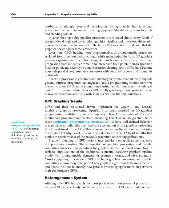
Th is appendix focuses on the GPU—the ubiquitous graphics processing unit in every PC, laptop, desktop computer, and workstation. In its most basic form, the GPU generates 2D and 3D graphics, images, and video that enable window-based operating systems, graphical user interfaces, video games, visual imaging applications, and video. Th e modern GPU that we describe here is a highly parallel, highly multithreaded multiprocessor optimized for visual computing. To provide real-time visual interaction with computed objects via graphics, images, and video, the GPU has a unifi ed graphics and computing architecture that serves as both a programmable graphics processor and a scalable parallel computing platform. PCs and game consoles combine a GPU with a CPU to form heterogeneous systems.
A Brief History of GPU EvolutionFift een years ago, there was no such thing as a GPU. Graphics on a PC were performed by a video graphics array (VGA) controller. A VGA controller was simply a memory controller and display generator connected to some DRAM. In the 1990s, semiconductor technology advanced suffi ciently that more functions could be added to the VGA controller. By 1997, VGA controllers were beginning to incorporate some three-dimensional (3D) acceleration functions, including
graphics processing unit (GPU) A processor optimized for 2D and 3D graphics, video, visual computing, and display.
visual computing A mix of graphics processing and computing that lets you visually interact with computed objects via graphics, images, and video.
heterogeneous system A system combining diff erent processor types. A PC is a heterogeneous CPU–GPU system.
C-4 Appendix C Graphics and Computing GPUs
hardware for triangle setup and rasterization (dicing triangles into individual pixels) and texture mapping and shading (applying “decals” or patterns to pixels and blending colors).
In 2000, the single chip graphics processor incorporated almost every detail of the traditional high-end workstation graphics pipeline and, therefore, deserved a new name beyond VGA controller. Th e term GPU was coined to denote that the graphics device had become a processor.
Over time, GPUs became more programmable, as programmable processors replaced fi xed function dedicated logic while maintaining the basic 3D graphics pipeline organization. In addition, computations became more precise over time, progressing from indexed arithmetic, to integer and fi xed point, to single precision fl oating-point, and recently to double precision fl oating-point. GPUs have become massively parallel programmable processors with hundreds of cores and thousands of threads.
Recently, processor instructions and memory hardware were added to support general purpose programming languages, and a programming environment was created to allow GPUs to be programmed using familiar languages, including C and C��. Th is innovation makes a GPU a fully general-purpose, programmable, manycore processor, albeit still with some special benefi ts and limitations.
GPU Graphics TrendsGPUs and their associated drivers implement the OpenGL and DirectX models of graphics processing. OpenGL is an open standard for 3D graphics programming available for most computers. DirectX is a series of Microsoft multimedia programming interfaces, including Direct3D for 3D graphics. Since these application programming interfaces (APIs) have well-defi ned behavior, it is possible to build eff ective hardware acceleration of the graphics processing functions defi ned by the APIs. Th is is one of the reasons (in addition to increasing device density) why new GPUs are being developed every 12 to 18 months that double the performance of the previous generation on existing applications.
Frequent doubling of GPU performance enables new applications that were not previously possible. Th e intersection of graphics processing and parallel computing invites a new paradigm for graphics, known as visual computing. It replaces large sections of the traditional sequential hardware graphics pipeline model with programmable elements for geometry, vertex, and pixel programs. Visual computing in a modern GPU combines graphics processing and parallel computing in novel ways that permit new graphics algorithms to be implemented, and opens the door to entirely new parallel processing applications on pervasive high-performance GPUs.
Heterogeneous SystemAlthough the GPU is arguably the most parallel and most powerful processor in a typical PC, it is certainly not the only processor. Th e CPU, now multicore and
application programming interface (API) A set of function and data structure defi nitions providing an interface to a library of functions.
C.1 Introduction C-5
soon to be manycore, is a complementary, primarily serial processor companion to the massively parallel manycore GPU. Together, these two types of processors comprise a heterogeneous multiprocessor system.
Th e best performance for many applications comes from using both the CPU and the GPU. Th is appendix will help you understand how and when to best split the work between these two increasingly parallel processors.
GPU Evolves into Scalable Parallel ProcessorGPUs have evolved functionally from hardwired, limited capability VGA controllers to programmable parallel processors. Th is evolution has proceeded by changing the logical (API-based) graphics pipeline to incorporate programmable elements and also by making the underlying hardware pipeline stages less specialized and more programmable. Eventually, it made sense to merge disparate programmable pipeline elements into one unifi ed array of many programmable processors.
In the GeForce 8-series generation of GPUs, the geometry, vertex, and pixel processing all run on the same type of processor. Th is unifi cation allows for dramatic scalability. More programmable processor cores increase the total system throughput. Unifying the processors also delivers very eff ective load balancing, since any processing function can use the whole processor array. At the other end of the spectrum, a processor array can now be built with very few processors, since all of the functions can be run on the same processors.
Why CUDA and GPU Computing?Th is uniform and scalable array of processors invites a new model of programming for the GPU. Th e large amount of fl oating-point processing power in the GPU processor array is very attractive for solving nongraphics problems. Given the large degree of parallelism and the range of scalability of the processor array for graphics applications, the programming model for more general computing must express the massive parallelism directly, but allow for scalable execution.
GPU computing is the term coined for using the GPU for computing via a parallel programming language and API, without using the traditional graphics API and graphics pipeline model. Th is is in contrast to the earlier General Purpose computation on GPU (GPGPU) approach, which involves programming the GPU using a graphics API and graphics pipeline to perform nongraphics tasks.
Compute Unifed Device Architecture (CUDA) is a scalable parallel programming model and soft ware platform for the GPU and other parallel processors that allows the programmer to bypass the graphics API and graphics interfaces of the GPU and simply program in C or C��. Th e CUDA programming model has an SPMD (single-program multiple data) soft ware style, in which a programmer writes a program for one thread that is instanced and executed by many threads in parallel on the multiple processors of the GPU. In fact, CUDA also provides a facility for programming multiple CPU cores as well, so CUDA is an environment for writing parallel programs for the entire heterogeneous computer system.
GPU computing Using a GPU for computing via a parallel programming language and API.
GPGPU Using a GPU for general-purpose computation via a traditional graphics API and graphics pipeline.
CUDA A scalable parallel programming model and language based on C/C��. It is a parallel programming platform for GPUs and multicore CPUs.

C-6 Appendix C Graphics and Computing GPUs
GPU Unifes Graphics and ComputingWith the addition of CUDA and GPU computing to the capabilities of the GPU, it is now possible to use the GPU as both a graphics processor and a computing processor at the same time, and to combine these uses in visual computing applications. Th e underlying processor architecture of the GPU is exposed in two ways: fi rst, as implementing the programmable graphics APIs, and second, as a massively parallel processor array programmable in C/C�� with CUDA.
Although the underlying processors of the GPU are unifi ed, it is not necessary that all of the SPMD thread programs are the same. Th e GPU can run graphics shader programs for the graphics aspect of the GPU, processing geometry, vertices, and pixels, and also run thread programs in CUDA.
Th e GPU is truly a versatile multiprocessor architecture, supporting a variety of processing tasks. GPUs are excellent at graphics and visual computing as they were specifi cally designed for these applications. GPUs are also excellent at many general-purpose throughput applications that are “fi rst cousins” of graphics, in that they perform a lot of parallel work, as well as having a lot of regular problem structure. In general, they are a good match to data-parallel problems (see Chapter 6), particularly large problems, but less so for less regular, smaller problems.
GPU Visual Computing ApplicationsVisual computing includes the traditional types of graphics applications plus many new applications. Th e original purview of a GPU was “anything with pixels,” but it now includes many problems without pixels but with regular computation and/or data structure. GPUs are eff ective at 2D and 3D graphics, since that is the purpose for which they are designed. Failure to deliver this application performance would be fatal. 2D and 3D graphics use the GPU in its “graphics mode,” accessing the processing power of the GPU through the graphics APIs, OpenGL™, and DirectX™. Games are built on the 3D graphics processing capability.
Beyond 2D and 3D graphics, image processing and video are important applications for GPUs. Th ese can be implemented using the graphics APIs or as computational programs, using CUDA to program the GPU in computing mode. Using CUDA, image processing is simply another data-parallel array program. To the extent that the data access is regular and there is good locality, the program will be effi cient. In practice, image processing is a very good application for GPUs. Video processing, especially encode and decode (compression and decompression according to some standard algorithms), is quite effi cient.
Th e greatest opportunity for visual computing applications on GPUs is to “break the graphics pipeline.” Early GPUs implemented only specifi c graphics APIs, albeit at very high performance. Th is was wonderful if the API supported the operations that you wanted to do. If not, the GPU could not accelerate your task, because early GPU functionality was immutable. Now, with the advent of GPU computing and CUDA, these GPUs can be programmed to implement a diff erent virtual pipeline by simply writing a CUDA program to describe the computation and data fl ow that
C.2 GPU System Architectures C-7
is desired. So, all applications are now possible, which will stimulate new visual computing approaches.
C.2 GPU System Architectures
In this section, we survey GPU system architectures in common use today. We discuss system confi gurations, GPU functions and services, standard programming interfaces, and a basic GPU internal architecture.
Heterogeneous CPU–GPU System ArchitectureA heterogeneous computer system architecture using a GPU and a CPU can be described at a high level by two primary characteristics: fi rst, how many functional subsystems and/or chips are used and what are their interconnection technologies and topology; and second, what memory subsystems are available to these functional subsystems. See Chapter 6 for background on the PC I/O systems and chip sets.
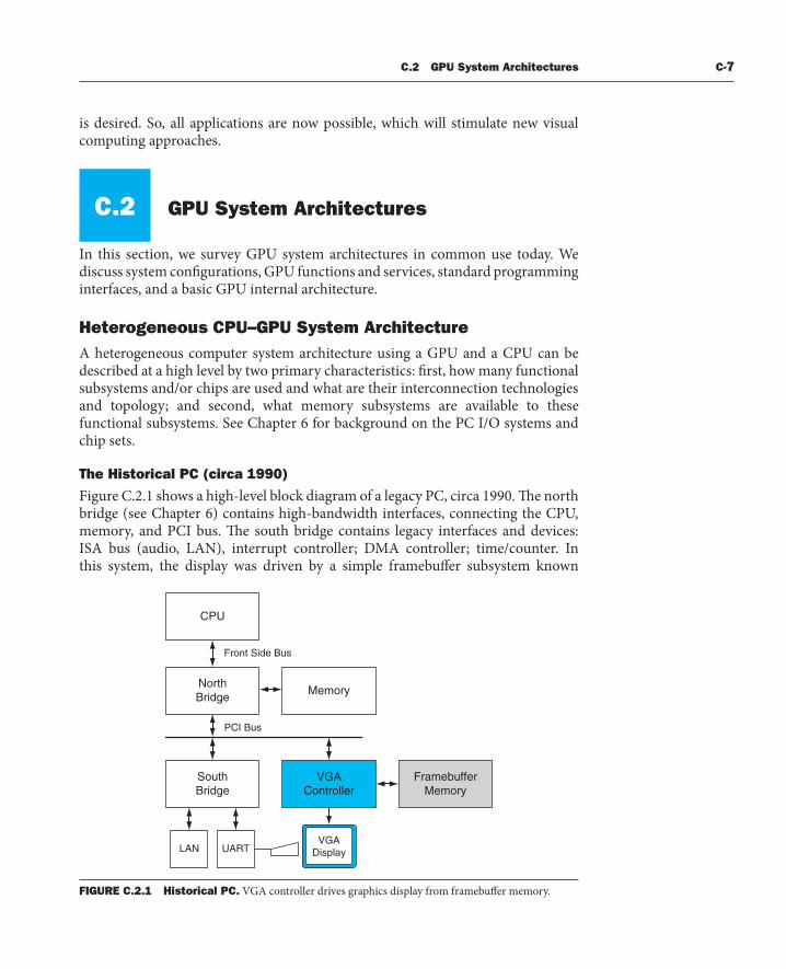
The Historical PC (circa 1990)
Figure C.2.1 shows a high-level block diagram of a legacy PC, circa 1990. Th e north bridge (see Chapter 6) contains high-bandwidth interfaces, connecting the CPU, memory, and PCI bus. Th e south bridge contains legacy interfaces and devices: ISA bus (audio, LAN), interrupt controller; DMA controller; time/counter. In this system, the display was driven by a simple framebuff er subsystem known
CPU
NorthBridge
SouthBridge
Front Side Bus
PCI Bus
FramebufferMemory
VGAController
Memory
UARTLANVGA
Display
FIGURE C.2.1 Historical PC. VGA controller drives graphics display from framebuff er memory.
C-8 Appendix C Graphics and Computing GPUs
as a VGA (video graphics array) which was attached to the PCI bus. Graphics subsystems with built-in processing elements (GPUs) did not exist in the PC landscape of 1990.
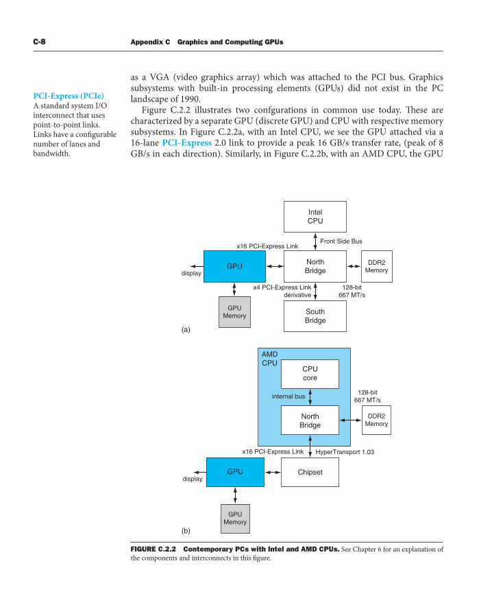
Figure C.2.2 illustrates two confgurations in common use today. Th ese are characterized by a separate GPU (discrete GPU) and CPU with respective memory subsystems. In Figure C.2.2a, with an Intel CPU, we see the GPU attached via a 16-lane PCI-Express 2.0 link to provide a peak 16 GB/s transfer rate, (peak of 8 GB/s in each direction). Similarly, in Figure C.2.2b, with an AMD CPU, the GPU
PCI-Express (PCIe) A standard system I/O interconnect that uses point-to-point links. Links have a confi gurable number of lanes and bandwidth.
Front Side Bus
GPUMemory
SouthBridge
NorthBridge
IntelCPU
DDR2Memory
x16 PCI-Express Link
x4 PCI-Express Linkderivative
128-bit667 MT/s
displayGPU
128-bit667 MT/s
internal bus
GPUMemory
DDR2Memory
x16 PCI-Express Link
Chipset
CPUcore
AMDCPU
GPU
NorthBridge
HyperTransport 1.03
display
(a)
(b)
FIGURE C.2.2 Contemporary PCs with Intel and AMD CPUs. See Chapter 6 for an explanation of the components and interconnects in this fi gure.

C.2 GPU System Architectures C-9
is attached to the chipset, also via PCI-Express with the same available bandwidth. In both cases, the GPUs and CPUs may access each other’s memory, albeit with less available bandwidth than their access to the more directly attached memories. In the case of the AMD system, the north bridge or memory controller is integrated into the same die as the CPU.
A low-cost variation on these systems, a unifi ed memory architecture (UMA) system, uses only CPU system memory, omitting GPU memory from the system. Th ese systems have relatively low performance GPUs, since their achieved performance is limited by the available system memory bandwidth and increased latency of memory access, whereas dedicated GPU memory provides high bandwidth and low latency.
A high performance system variation uses multiple attached GPUs, typically two to four working in parallel, with their displays daisy-chained. An example is the NVIDIA SLI (scalable link interconnect) multi-GPU system, designed for high performance gaming and workstations.
Th e next system category integrates the GPU with the north bridge (Intel) or chipset (AMD) with and without dedicated graphics memory.
Chapter 5 explains how caches maintain coherence in a shared address space. With CPUs and GPUs, there are multiple address spaces. GPUs can access their own physical local memory and the CPU system’s physical memory using virtual addresses that are translated by an MMU on the GPU. Th e operating system kernel manages the GPU’s page tables. A system physical page can be accessed using either coherent or noncoherent PCI-Express transactions, determined by an attribute in the GPU’s page table. Th e CPU can access GPU’s local memory through an address range (also called aperture) in the PCI-Express address space.
Game Consoles
Console systems such as the Sony PlayStation 3 and the Microsoft Xbox 360 resemble the PC system architectures previously described. Console systems are designed to be shipped with identical performance and functionality over a lifespan that can last fi ve years or more. During this time, a system may be reimplemented many times to exploit more advanced silicon manufacturing processes and thereby to provide constant capability at ever lower costs. Console systems do not need to have their subsystems expanded and upgraded the way PC systems do, so the major internal system buses tend to be customized rather than standardized.
GPU Interfaces and DriversIn a PC today, GPUs are attached to a CPU via PCI-Express. Earlier generations used AGP. Graphics applications call OpenGL [Segal and Akeley, 2006] or Direct3D [Microsoft DirectX Specifcation] API functions that use the GPU as a coprocessor. Th e APIs send commands, programs, and data to the GPU via a graphics device driver optimized for the particular GPU.
unifi ed memory architecture (UMA) A system architecture in which the CPU and GPU share a common system memory.
AGP An extended version of the original PCI I/O bus, which provided up to eight times the bandwidth of the original PCI bus to a single card slot. Its primary purpose was to connect graphics subsystems into PC systems.
C-10 Appendix C Graphics and Computing GPUs
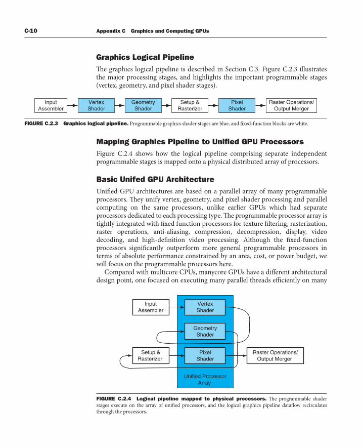
Mapping Graphics Pipeline to Unifi ed GPU ProcessorsFigure C.2.4 shows how the logical pipeline comprising separate independent programmable stages is mapped onto a physical distributed array of processors.
Basic Unifed GPU ArchitectureUnifi ed GPU architectures are based on a parallel array of many programmable processors. Th ey unify vertex, geometry, and pixel shader processing and parallel computing on the same processors, unlike earlier GPUs which had separate processors dedicated to each processing type. Th e programmable processor array is tightly integrated with fi xed function processors for texture fi ltering, rasterization, raster operations, anti-aliasing, compression, decompression, display, video decoding, and high-defi nition video processing. Although the fi xed-function processors signifi cantly outperform more general programmable processors in terms of absolute performance constrained by an area, cost, or power budget, we will focus on the programmable processors here.
Compared with multicore CPUs, manycore GPUs have a diff erent architectural design point, one focused on executing many parallel threads effi ciently on many
InputAssembler
VertexShader
GeometryShader
Setup &Rasterizer
PixelShader
Raster Operations/Output Merger
FIGURE C.2.3 Graphics logical pipeline. Programmable graphics shader stages are blue, and fi xed-function blocks are white.
Unified ProcessorArray
InputAssembler
VertexShader
Setup &Rasterizer
Raster Operations/Output Merger
GeometryShader
PixelShader
FIGURE C.2.4 Logical pipeline mapped to physical processors. Th e programmable shader stages execute on the array of unifi ed processors, and the logical graphics pipeline datafl ow recirculates through the processors.
Graphics Logical PipelineTh e graphics logical pipeline is described in Section C.3. Figure C.2.3 illustrates the major processing stages, and highlights the important programmable stages (vertex, geometry, and pixel shader stages).

C.2 GPU System Architectures C-11
processor cores. By using many simpler cores and optimizing for data-parallel behavior among groups of threads, more of the per-chip transistor budget is devoted to computation, and less to on-chip caches and overhead.
Processor Array
A unifi ed GPU processor array contains many processor cores, typically organized into multithreaded multiprocessors. Figure C.2.5 shows a GPU with an array of 112 streaming processor (SP) cores, organized as 14 multithreaded streaming multiprocessors (SMs). Each SP core is highly multithreaded, managing 96 concurrent threads and their state in hardware. Th e processors connect with four 64-bit-wide DRAM partitions via an interconnection network. Each SM has eight SP cores, two special function units (SFUs), instruction and constant caches, a multithreaded instruction unit, and a shared memory. Th is is the basic Tesla architecture implemented by the NVIDIA GeForce 8800. It has a unifi ed architecture in which the traditional graphics programs for vertex, geometry, and pixel shading run on the unifi ed SMs and their SP cores, and computing programs run on the same processors.
GPU
Host CPU System Memory
DRAM
ROP L2
DRAM
ROP L2
DRAM
ROP L2
DRAM
ROP L2
TPC
Texture UnitTex L1
SM
SP SP
SP SP
SP SP
SP SP
SM
SP SP
SP SP
SP SP
SP SP
TPC
Texture UnitTex L1
SM
SP SP
SP SP
SP SP
SP SP
SM
SP SP
SP SP
SP SP
SP SP
TPC
Texture UnitTex L1
SM
SP SP
SP SP
SP SP
SP SP
SM
SP SP
SP SP
SP SP
SP SP
TPC
Texture UnitTex L1
SM
SP SP
SP SP
SP SP
SP SP
SM
SP SP
SP SP
SP SP
SP SP
TPC
Texture UnitTex L1
SM
SP SP
SP SP
SP SP
SP SP
SM
SP SP
SP SP
SP SP
SP SP
TPC
Texture UnitTex L1
SM
SP SP
SP SP
SP SP
SP SP
SM
SP SP
SP SP
SP SP
SP SP
TPC
Texture UnitTex L1
SM
SP SP
SP SP
SP SP
SP SP
SM
SP SP
SP SP
SP SP
SP SP
Vertex WorkDistribution
Input Assembler
Host Interface
Bridge
Pixel WorkDistribution
Viewport/Clip/Setup/Raster/
ZCull
Compute WorkDistribution
SP
SharedMemory
SP
SP SP
SP SP
SP
SM
SP
I-Cache
MT Issue
C-Cache
SFU SFU
Interconnection Network
Display Interface
Display
High-DefinitionVideo Processors
SharedMemory
SharedMemory
SharedMemory
SharedMemory
SharedMemory
SharedMemory
SharedMemory
SharedMemory
SharedMemory
SharedMemory
SharedMemory
SharedMemory
SharedMemory
SharedMemory
FIGURE C.2.5 Basic unifi ed GPU architecture. Example GPU with 112 streaming processor (SP) cores organized in 14 streaming multiprocessors (SMs); the cores are highly multithreaded. It has the basic Tesla architecture of an NVIDIA GeForce 8800. Th e processors connect with four 64-bit-wide DRAM partitions via an interconnection network. Each SM has eight SP cores, two special function units (SFUs), instruction and constant caches, a multithreaded instruction unit, and a shared memory.

C-12 Appendix C Graphics and Computing GPUs
Th e processor array architecture is scalable to smaller and larger GPU confi gurations by scaling the number of multiprocessors and the number of memory partitions. Figure C.2.5 shows seven clusters of two SMs sharing a texture unit and a texture L1 cache. Th e texture unit delivers fi ltered results to the SM given a set of coordinates into a texture map. Because fi lter regions of support oft en overlap for successive texture requests, a small streaming L1 texture cache is eff ective to reduce the number of requests to the memory system. Th e processor array connects with raster operation processors (ROPs), L2 texture caches, external DRAM memories, and system memory via a GPU-wide interconnection network. Th e number of processors and number of memories can scale to design balanced GPU systems for diff erent performance and market segments.
C.3 Programming GPUs
Programming multiprocessor GPUs is qualitatively diff erent than programming other multiprocessors like multicore CPUs. GPUs provide two to three orders of magnitude more thread and data parallelism than CPUs, scaling to hundreds of processor cores and tens of thousands of concurrent threads. GPUs continue to increase their parallelism, doubling it about every 12 to 18 months, enabled by Moore’s law [1965] of increasing integrated circuit density and by improving architectural effi ciency. To span the wide price and performance range of diff erent market segments, diff erent GPU products implement widely varying numbers of processors and threads. Yet users expect games, graphics, imaging, and computing applications to work on any GPU, regardless of how many parallel threads it executes or how many parallel processor cores it has, and they expect more expensive GPUs (with more threads and cores) to run applications faster. As a result, GPU programming models and application programs are designed to scale transparently to a wide range of parallelism.
Th e driving force behind the large number of parallel threads and cores in a GPU is real-time graphics performance—the need to render complex 3D scenes with high resolution at interactive frame rates, at least 60 frames per second. Correspondingly, the scalable programming models of graphics shading languages such as Cg (C for graphics) and HLSL (high-level shading language) are designed to exploit large degrees of parallelism via many independent parallel threads and to scale to any number of processor cores. Th e CUDA scalable parallel programming model similarly enables general parallel computing applications to leverage large numbers of parallel threads and scale to any number of parallel processor cores, transparently to the application.
In these scalable programming models, the programmer writes code for a single thread, and the GPU runs myriad thread instances in parallel. Programs thus scale transparently over a wide range of hardware parallelism. Th is simple paradigm arose from graphics APIs and shading languages that describe how to shade one

C.3 Programming GPUs C-13
vertex or one pixel. It has remained an eff ective paradigm as GPUs have rapidly increased their parallelism and performance since the late 1990s.
Th is section briefl y describes programming GPUs for real-time graphics applications using graphics APIs and programming languages. It then describes programming GPUs for visual computing and general parallel computing applications using the C language and the CUDA programming model.
Programming Real-Time GraphicsAPIs have played an important role in the rapid, successful development of GPUs and processors. Th ere are two primary standard graphics APIs: OpenGL and Direct3D, one of the Microsoft DirectX multimedia programming interfaces. OpenGL, an open standard, was originally proposed and defi ned by Silicon Graphics Incorporated. Th e ongoing development and extension of the OpenGL standard [Segal and Akeley, 2006], [Kessenich, 2006] is managed by Khronos, an industry consortium. Direct3D [Blythe, 2006], a de facto standard, is defi ned and evolved forward by Microsoft and partners. OpenGL and Direct3D are similarly structured, and continue to evolve rapidly with GPU hardware advances. Th ey defi ne a logical graphics processing pipeline that is mapped onto the GPU hardware and processors, along with programming models and languages for the programmable pipeline stages.
Logical Graphics PipelineFigure C.3.1 illustrates the Direct3D 10 logical graphics pipeline. OpenGL has a similar graphics pipeline structure. Th e API and logical pipeline provide a streaming datafl ow infrastructure and plumbing for the programmable shader stages, shown in blue. Th e 3D application sends the GPU a sequence of vertices grouped into geometric primitives—points, lines, triangles, and polygons. Th e input assembler collects vertices and primitives. Th e vertex shader program executes per-vertex processing,
OpenGL An open-standard graphics API.
Direct3D A graphics API defi ned by Microsoft and partners.
InputAssembler
VertexShader
GeometryShader
Setup &Rasterizer
PixelShader
Raster Operations/Output Merger
VertexBuffer
Texture Texture Texture RenderTarget
Sampler Sampler Sampler
Constant
DepthZ-Buffer
Constant Constant
StreamBuffer
StreamOut
Index BufferMemory
Stencil
GPU
FIGURE C.3.1 Direct3D 10 graphics pipeline. Each logical pipeline stage maps to GPU hardware or to a GPU processor. Programmable shader stages are blue, fi xed-function blocks are white, and memory objects are gray. Each stage processes a vertex, geometric primitive, or pixel in a streaming datafl ow fashion.
C-14 Appendix C Graphics and Computing GPUs
including transforming the vertex 3D position into a screen position and lighting the vertex to determine its color. Th e geometry shader program executes per-primitive processing and can add or drop primitives. Th e setup and rasterizer unit generates pixel fragments (fragments are potential contributions to pixels) that are covered by a geometric primitive. Th e pixel shader program performs per-fragment processing, including interpolating per-fragment parameters, texturing, and coloring. Pixel shaders make extensive use of sampled and fi ltered lookups into large 1D, 2D, or 3D arrays called textures, using interpolated fl oating-point coordinates. Shaders use texture accesses for maps, functions, decals, images, and data. Th e raster operations processing (or output merger) stage performs Z-buff er depth testing and stencil testing, which may discard a hidden pixel fragment or replace the pixel’s depth with the fragment’s depth, and performs a color blending operation that combines the fragment color with the pixel color and writes the pixel with the blended color.
Th e graphics API and graphics pipeline provide input, output, memory objects, and infrastructure for the shader programs that process each vertex, primitive, and pixel fragment.
Graphics Shader ProgramsReal-time graphics applications use many diff erent shader programs to model how light interacts with diff erent materials and to render complex lighting and shadows. Shading languages are based on a datafl ow or streaming programming model that corresponds with the logical graphics pipeline. Vertex shader programs map the position of triangle vertices onto the screen, altering their position, color, or orientation. Typically a vertex shader thread inputs a fl oating-point (x, y, z, w) vertex position and computes a fl oating-point (x, y, z) screen position. Geometry shader programs operate on geometric primitives (such as lines and triangles) defi ned by multiple vertices, changing them or generating additional primitives. Pixel fragment shaders each “shade” one pixel, computing a fl oating-point red, green, blue, alpha (RGBA) color contribution to the rendered image at its pixel sample (x, y) image position. Shaders (and GPUs) use fl oating-point arithmetic for all pixel color calculations to eliminate visible artifacts while computing the extreme range of pixel contribution values encountered while rendering scenes with complex lighting, shadows, and high dynamic range. For all three types of graphics shaders, many program instances can be run in parallel, as independent parallel threads, because each works on independent data, produces independent results, and has no side eff ects. Independent vertices, primitives, and pixels further enable the same graphics program to run on diff erently sized GPUs that process diff erent numbers of vertices, primitives, and pixels in parallel. Graphics programs thus scale transparently to GPUs with diff erent amounts of parallelism and performance.
Users program all three logical graphics threads with a common targeted high-level language. HLSL (high-level shading language) and Cg (C for graphics) are commonly used. Th ey have C-like syntax and a rich set of library functions for matrix operations, trigonometry, interpolation, and texture access and fi ltering, but are far from general computing languages: they currently lack general memory
texture A 1D, 2D, or 3D array that supports sampled and fi ltered lookups with interpolated coordinates.
shader A program that operates on graphics data such as a vertex or a pixel fragment.
shading language A graphics rendering language, usually having a datafl ow or streaming programming model.
C.3 Programming GPUs C-15
access, pointers, fi le I/O, and recursion. HLSL and Cg assume that programs live within a logical graphics pipeline, and thus I/O is implicit. For example, a pixel fragment shader may expect the geometric normal and multiple texture coordinates to have been interpolated from vertex values by upstream fi xed-function stages and can simply assign a value to the COLOR output parameter to pass it downstream to be blended with a pixel at an implied (x, y) position.
Th e GPU hardware creates a new independent thread to execute a vertex, geometry, or pixel shader program for every vertex, every primitive, and every pixel fragment. In video games, the bulk of threads execute pixel shader programs, as there are typically 10 to 20 times or more pixel fragments than vertices, and complex lighting and shadows require even larger ratios of pixel to vertex shader threads. Th e graphics shader programming model drove the GPU architecture to effi ciently execute thousands of independent fi ne-grained threads on many parallel processor cores.
Pixel Shader ExampleConsider the following Cg pixel shader program that implements the “environment mapping” rendering technique. For each pixel thread, this shader is passed fi ve parameters, including 2D fl oating-point texture image coordinates needed to sample the surface color, and a 3D fl oating-point vector giving the refection of the view direction off the surface. Th e other three “uniform” parameters do not vary from one pixel instance (thread) to the next. Th e shader looks up color in two texture images: a 2D texture access for the surface color, and a 3D texture access into a cube map (six images corresponding to the faces of a cube) to obtain the external world color corresponding to the refection direction. Th en the fi nal four-component (red, green, blue, alpha) fl oating-point color is computed using a weighted average called a “lerp” or linear interpolation function.
void refection( float2 texCoord : TEXCOORD0, float3 refection_dir : TEXCOORD1, out float4 color : COLOR, uniform float shiny, uniform sampler2D surfaceMap, uniform samplerCUBE envMap){// Fetch the surface color from a texture float4 surfaceColor = tex2D(surfaceMap, texCoord);
// Fetch reflected color by sampling a cube map float4 reflectedColor = texCUBE(environmentMap, refection_dir);
// Output is weighted average of the two colors color = lerp(surfaceColor, refectedColor, shiny);}
C-16 Appendix C Graphics and Computing GPUs
Although this shader program is only three lines long, it activates a lot of GPU hardware. For each texture fetch, the GPU texture subsystem makes multiple memory accesses to sample image colors in the vicinity of the sampling coordinates, and then interpolates the fi nal result with fl oating-point fi ltering arithmetic. Th e multithreaded GPU executes thousands of these lightweight Cg pixel shader threads in parallel, deeply interleaving them to hide texture fetch and memory latency.
Cg focuses the programmer’s view to a single vertex or primitive or pixel, which the GPU implements as a single thread; the shader program transparently scales to exploit thread parallelism on the available processors. Being application-specifi c, Cg provides a rich set of useful data types, library functions, and language constructs to express diverse rendering techniques.
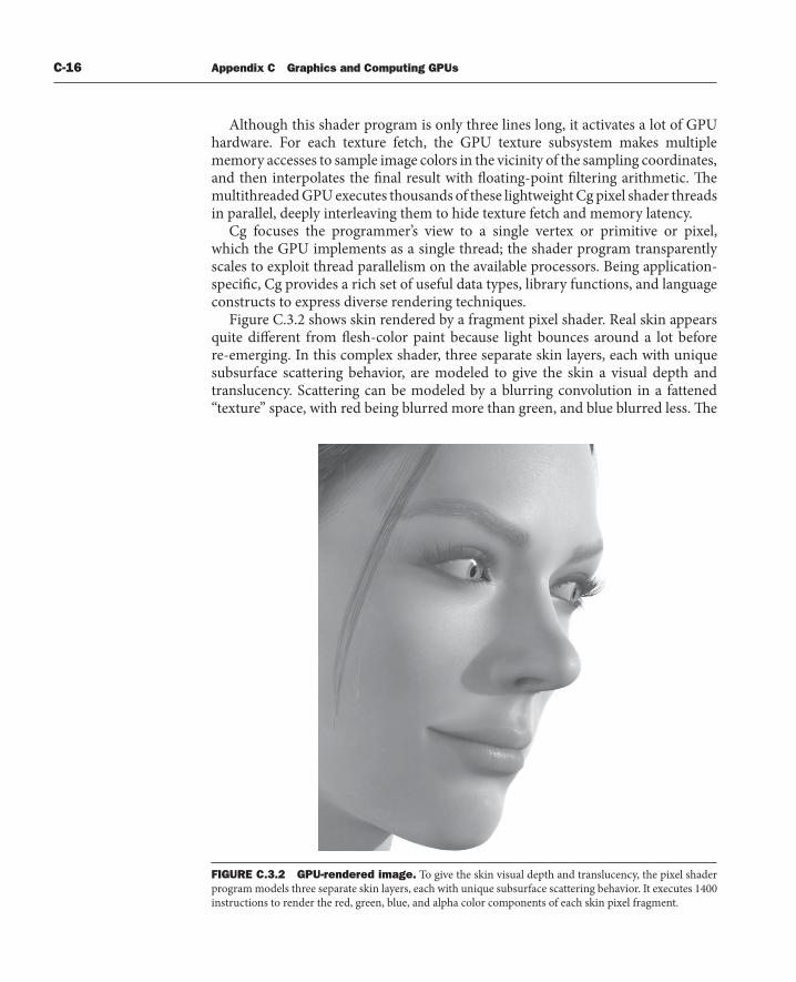
Figure C.3.2 shows skin rendered by a fragment pixel shader. Real skin appears quite diff erent from fl esh-color paint because light bounces around a lot before re-emerging. In this complex shader, three separate skin layers, each with unique subsurface scattering behavior, are modeled to give the skin a visual depth and translucency. Scattering can be modeled by a blurring convolution in a fattened “texture” space, with red being blurred more than green, and blue blurred less. Th e
FIGURE C.3.2 GPU-rendered image. To give the skin visual depth and translucency, the pixel shader program models three separate skin layers, each with unique subsurface scattering behavior. It executes 1400 instructions to render the red, green, blue, and alpha color components of each skin pixel fragment.

C.3 Programming GPUs C-17
compiled Cg shader executes 1400 instructions to compute the color of one skin pixel.
As GPUs have evolved superior fl oating-point performance and very high streaming memory bandwidth for real-time graphics, they have attracted highly parallel applications beyond traditional graphics. At fi rst, access to this power was available only by couching an application as a graphics-rendering algorithm, but this GPGPU approach was oft en awkward and limiting. More recently, the CUDA programming model has provided a far easier way to exploit the scalable high-performance fl oating-point and memory bandwidth of GPUs with the C programming language.
Programming Parallel Computing ApplicationsCUDA, Brook, and CAL are programming interfaces for GPUs that are focused on data parallel computation rather than on graphics. CAL (Compute Abstraction Layer) is a low-level assembler language interface for AMD GPUs. Brook is a streaming language adapted for GPUs by Buck et al. [2004]. CUDA, developed by NVIDIA [2007], is an extension to the C and C�� languages for scalable parallel programming of manycore GPUs and multicore CPUs. Th e CUDA programming model is described below, adapted from an article by Nickolls et al. [2008].
With the new model the GPU excels in data parallel and throughput computing, executing high performance computing applications as well as graphics applications.
Data Parallel Problem Decomposition
To map large computing problems eff ectively to a highly parallel processing architecture, the programmer or compiler decomposes the problem into many small problems that can be solved in parallel. For example, the programmer partitions a large result data array into blocks and further partitions each block into elements, such that the result blocks can be computed independently in parallel, and the elements within each block are computed in parallel. Figure C.3.3 shows a decomposition of a result data array into a 3 � 2 grid of blocks, where each block is further decomposed into a 5 � 3 array of elements. Th e two-level parallel decomposition maps naturally to the GPU architecture: parallel multiprocessors compute result blocks, and parallel threads compute result elements.
Th e programmer writes a program that computes a sequence of result data grids, partitioning each result grid into coarse-grained result blocks that can be computed independently in parallel. Th e program computes each result block with an array of fi ne-grained parallel threads, partitioning the work among threads so that each computes one or more result elements.
Scalable Parallel Programming with CUDATh e CUDA scalable parallel programming model extends the C and C�� languages to exploit large degrees of parallelism for general applications on highly parallel multiprocessors, particularly GPUs. Early experience with CUDA shows

C-18 Appendix C Graphics and Computing GPUs
that many sophisticated programs can be readily expressed with a few easily understood abstractions. Since NVIDIA released CUDA in 2007, developers have rapidly developed scalable parallel programs for a wide range of applications, including seismic data processing, computational chemistry, linear algebra, sparse matrix solvers, sorting, searching, physics models, and visual computing. Th ese applications scale transparently to hundreds of processor cores and thousands of concurrent threads. NVIDIA GPUs with the Tesla unifi ed graphics and computing architecture (described in Sections C.4 and C.7) run CUDA C programs, and are widely available in laptops, PCs, workstations, and servers. Th e CUDA model is also applicable to other shared memory parallel processing architectures, including multicore CPUs.
CUDA provides three key abstractions—a hierarchy of thread groups, shared memories, and barrier synchronization—that provide a clear parallel structure to conventional C code for one thread of the hierarchy. Multiple levels of threads, memory, and synchronization provide fi ne-grained data parallelism and thread parallelism, nested within coarse-grained data parallelism and task parallelism. Th e abstractions guide the programmer to partition the problem into coarse subproblems that can be solved independently in parallel, and then into fi ner pieces that can be solved in parallel. Th e programming model scales transparently to large numbers of processor cores: a compiled CUDA program executes on any number of processors, and only the runtime system needs to know the physical processor count.
Step 1:
Sequence
Blo(0,
Blo(0,
Step 2:
Result Data Grid 1
ck0)
Block(1, 0)
Block(1, 1)
Block(2, 0)
Block(2, 1)
Block (1, 1)
Elem(0, 0)
Elem(1, 0)
Elem(2, 0)
Elem(3, 0)
Elem(4, 0)
Elem(0, 1)
Elem(1, 1)
Elem(2, 1)
Elem(3, 1)
Elem(4, 1)
Elem(0, 2)
Elem(1, 2)
Elem(2, 2)
Elem(3, 2)
Elem(4, 2)
ck1)
Result Data Grid 2
FIGURE C.3.3 Decomposing result data into a grid of blocks of elements to be computed in parallel.

C.3 Programming GPUs C-19
The CUDA Paradigm
CUDA is a minimal extension of the C and C�� programming languages. Th e programmer writes a serial program that calls parallel kernels, which may be simple functions or full programs. A kernel executes in parallel across a set of parallel threads. Th e programmer organizes these threads into a hierarchy of thread blocks and grids of thread blocks. A thread block is a set of concurrent threads that can cooperate among themselves through barrier synchronization and through shared access to a memory space private to the block. A grid is a set of thread blocks that may each be executed independently and thus may execute in parallel.
When invoking a kernel, the programmer specifi es the number of threads per block and the number of blocks comprising the grid. Each thread is given a unique thread ID number threadIdx within its thread block, numbered 0, 1, 2, ..., blockDim-1, and each thread block is given a unique block ID number blockIdx within its grid. CUDA supports thread blocks containing up to 512 threads. For convenience, thread blocks and grids may have 1, 2, or 3 dimensions, accessed via .x, .y, and .z index fi elds.
As a very simple example of parallel programming, suppose that we are given two vectors x and y of n fl oating-point numbers each and that we wish to compute the result of y � ax � y for some scalar value a. Th is is the so-called SAXPY kernel defi ned by the BLAS linear algebra library. Figure C.3.4 shows C code for performing this computation on both a serial processor and in parallel using CUDA.
Th e __global__ declaration specifi er indicates that the procedure is a kernel entry point. CUDA programs launch parallel kernels with the extended function call syntax:
kernel<<<dimGrid, dimBlock>>>(... parameter list ...);
where dimGrid and dimBlock are three-element vectors of type dim3 that specify the dimensions of the grid in blocks and the dimensions of the blocks in threads, respectively. Unspecifi ed dimensions default to one.
In Figure C.3.4, we launch a grid of n threads that assigns one thread to each element of the vectors and puts 256 threads in each block. Each individual thread computes an element index from its thread and block IDs and then performs the desired calculation on the corresponding vector elements. Comparing the serial and parallel versions of this code, we see that they are strikingly similar. Th is represents a fairly common pattern. Th e serial code consists of a loop where each iteration is independent of all the others. Such loops can be mechanically transformed into parallel kernels: each loop iteration becomes an independent thread. By assigning a single thread to each output element, we avoid the need for any synchronization among threads when writing results to memory.
Th e text of a CUDA kernel is simply a C function for one sequential thread. Th us, it is generally straightforward to write and is typically simpler than writing parallel code for vector operations. Parallelism is determined clearly and explicitly by specifying the dimensions of a grid and its thread blocks when launching a kernel.
kernel A program or function for one thread, designed to be executed by many threads.
thread block A set of concurrent threads that execute the same thread program and may cooperate to compute a result.
grid A set of thread blocks that execute the same kernel program.
C-20 Appendix C Graphics and Computing GPUs
Parallel execution and thread management is automatic. All thread creation, scheduling, and termination is handled for the programmer by the underlying system. Indeed, a Tesla architecture GPU performs all thread management directly in hardware. Th e threads of a block execute concurrently and may synchronize at a synchronization barrier by calling the __syncthreads() intrinsic. Th is guarantees that no thread in the block can proceed until all threads in the block have reached the barrier. Aft er passing the barrier, these threads are also guaranteed to see all writes to memory performed by threads in the block before the barrier. Th us, threads in a block may communicate with each other by writing and reading per-block shared memory at a synchronization barrier.
Since threads in a block may share memory and synchronize via barriers, they will reside together on the same physical processor or multiprocessor. Th e number of thread blocks can, however, greatly exceed the number of processors. Th e CUDA thread programming model virtualizes the processors and gives the programmer the fl exibility to parallelize at whatever granularity is most convenient. Virtualization
synchronization barrier Th reads wait at a synchronization barrier until all threads in the thread block arrive at the barrier.
FIGURE C.3.4 Sequential code (top) in C versus parallel code (bottom) in CUDA for SAXPY (see Chapter 6). CUDA parallel threads replace the C serial loop—each thread computes the same result as one loop iteration. Th e parallel code computes n results with n threads organized in blocks of 256 threads.
Computing y = ax + y with a serial loop:
void saxpy_serial(int n, float alpha, float *x, float *y){ for(int i = 0; i<n; ++i) y[i] = alpha*x[i] + y[i];}// Invoke serial SAXPY kernelsaxpy_serial(n, 2.0, x, y);
Computing y = ax + y in parallel using CUDA:
__global__void saxpy_parallel(int n, float alpha, float *x, float *y){ int i = blockIdx.x*blockDim.x + threadIdx.x;
if( i<n ) y[i] = alpha*x[i] + y[i];}
// Invoke parallel SAXPY kernel (256 threads per block)int nblocks = (n + 255) / 256;saxpy_parallel<<<nblocks, 256>>>(n, 2.0, x, y);
C.3 Programming GPUs C-21
into threads and thread blocks allows intuitive problem decompositions, as the number of blocks can be dictated by the size of the data being processed rather than by the number of processors in the system. It also allows the same CUDA program to scale to widely varying numbers of processor cores.
To manage this processing element virtualization and provide scalability, CUDA requires that thread blocks be able to execute independently. It must be possible to execute blocks in any order, in parallel or in series. Diff erent blocks have no means of direct communication, although they may coordinate their activities using atomic memory operations on the global memory visible to all threads—by atomically incrementing queue pointers, for example. Th is independence requirement allows thread blocks to be scheduled in any order across any number of cores, making the CUDA model scalable across an arbitrary number of cores as well as across a variety of parallel architectures. It also helps to avoid the possibility of deadlock. An application may execute multiple grids either independently or dependently. Independent grids may execute concurrently, given suffi cient hardware resources. Dependent grids execute sequentially, with an implicit interkernel barrier between them, thus guaranteeing that all blocks of the fi rst grid complete before any block of the second, dependent grid begins.
Th reads may access data from multiple memory spaces during their execution. Each thread has a private local memory. CUDA uses local memory for thread-private variables that do not fi t in the thread’s registers, as well as for stack frames and register spilling. Each thread block has a shared memory, visible to all threads of the block, which has the same lifetime as the block. Finally, all threads have access to the same global memory. Programs declare variables in shared and global memory with the __shared__ and __device__ type qualifers. On a Tesla architecture GPU, these memory spaces correspond to physically separate memories: per-block shared memory is a low-latency on-chip RAM, while global memory resides in the fast DRAM on the graphics board.
Shared memory is expected to be a low-latency memory near each processor, much like an L1 cache. It can therefore provide high-performance communication and data sharing among the threads of a thread block. Since it has the same lifetime as its corresponding thread block, kernel code will typically initialize data in shared variables, compute using shared variables, and copy shared memory results to global memory. Th read blocks of sequentially dependent grids communicate via global memory, using it to read input and write results.
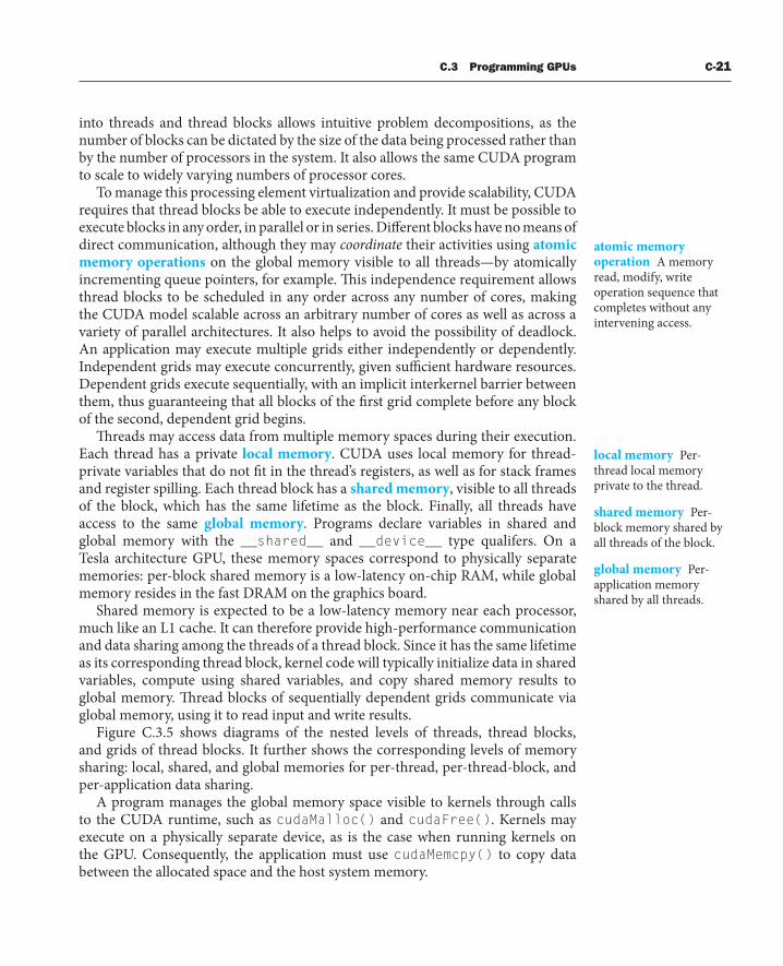
Figure C.3.5 shows diagrams of the nested levels of threads, thread blocks, and grids of thread blocks. It further shows the corresponding levels of memory sharing: local, shared, and global memories for per-thread, per-thread-block, and per-application data sharing.
A program manages the global memory space visible to kernels through calls to the CUDA runtime, such as cudaMalloc() and cudaFree(). Kernels may execute on a physically separate device, as is the case when running kernels on the GPU. Consequently, the application must use cudaMemcpy() to copy data between the allocated space and the host system memory.
atomic memory operation A memory read, modify, write operation sequence that completes without any intervening access.
local memory Per-thread local memory private to the thread.
shared memory Per-block memory shared by all threads of the block.
global memory Per-application memory shared by all threads.
C-22 Appendix C Graphics and Computing GPUs
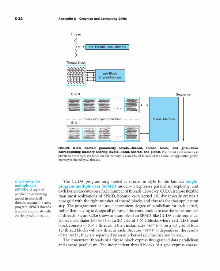
Th e CUDA programming model is similar in style to the familiar single- program multiple data (SPMD) model—it expresses parallelism explicitly, and each kernel executes on a fi xed number of threads. However, CUDA is more fl exible than most realizations of SPMD, because each kernel call dynamically creates a new grid with the right number of thread blocks and threads for that application step. Th e programmer can use a convenient degree of parallelism for each kernel, rather than having to design all phases of the computation to use the same number of threads. Figure C.3.6 shows an example of an SPMD-like CUDA code sequence. It fi rst instantiates kernelF on a 2D grid of 3 � 2 blocks where each 2D thread block consists of 5 � 3 threads. It then instantiates kernelG on a 1D grid of four 1D thread blocks with six threads each. Because kernelG depends on the results of kernelF, they are separated by an interkernel synchronization barrier.
Th e concurrent threads of a thread block express fi ne-grained data parallelism and thread parallelism. Th e independent thread blocks of a grid express coarse-
single-program multiple data (SPMD) A style of parallel programming model in which all threads execute the same program. SPMD threads typically coordinate with barrier synchronization.
Thread
per-Thread Local Memory
Thread Block
per-BlockShared Memory
Grid 0
. . .
Grid 1
. . .
Global Memory
Sequence
Inter-Grid Synchronization
FIGURE C.3.5 Nested granularity levels—thread, thread block, and grid—have corresponding memory sharing levels—local, shared, and global. Per-thread local memory is private to the thread. Per-block shared memory is shared by all threads of the block. Per-application global memory is shared by all threads.

C.3 Programming GPUs C-23
grained data parallelism. Independent grids express coarse-grained task parallelism. A kernel is simply C code for one thread of the hierarchy.
RestrictionsFor effi ciency, and to simplify its implementation, the CUDA programming model has some restrictions. Th reads and thread blocks may only be created by invoking a parallel kernel, not from within a parallel kernel. Together with the required independence of thread blocks, this makes it possible to execute CUDA programs
FIGURE C.3.6 Sequence of kernel F instantiated on a 2D grid of 2D thread blocks, an interkernel synchronization barrier, followed by kernel G on a 1D grid of 1D thread blocks.
kernelG 1D Grid is 4 thread blocks; each block is 6 threads
Sequence
Interkernel Synchronization Barrier
Block 2
Thread 5Thread 0 Thread 1 Thread 2 Thread 3 Thread 4
kernelF<<<(3, 2), (5, 3)>>>(params);
kernelF 2D Grid is 3 2 thread blocks; each block is 5 3 threads
Block 1, 1
Thread 0, 0 Thread 1, 0 Thread 2, 0 Thread 3, 0 Thread 4, 0
Thread 0, 1 Thread 1, 1 Thread 2, 1 Thread 3, 1 Thread 4, 1
Thread 0, 2 Thread 1, 2 Thread 2, 2 Thread 3, 2 Thread 4, 2
Block 0, 1 Block 2, 1Block 1, 1
Block 0, 0 Block 2, 0Block 1, 0
kernelG<<<4, 6>>>(params);
Block 0 Block 2Block 1 Block 3
C-24 Appendix C Graphics and Computing GPUs
with a simple scheduler that introduces minimal runtime overhead. In fact, the Tesla GPU architecture implements hardware management and scheduling of threads and thread blocks.
Task parallelism can be expressed at the thread block level but is diffi cult to express within a thread block because thread synchronization barriers operate on all the threads of the block. To enable CUDA programs to run on any number of processors, dependencies among thread blocks within the same kernel grid are not allowed—blocks must execute independently. Since CUDA requires that thread blocks be independent and allows blocks to be executed in any order, combining results generated by multiple blocks must in general be done by launching a second kernel on a new grid of thread blocks (although thread blocks may coordinate their activities using atomic memory operations on the global memory visible to all threads—by atomically incrementing queue pointers, for example).
Recursive function calls are not currently allowed in CUDA kernels. Recursion is unattractive in a massively parallel kernel, because providing stack space for the tens of thousands of threads that may be active would require substantial amounts of memory. Serial algorithms that are normally expressed using recursion, such as quicksort, are typically best implemented using nested data parallelism rather than explicit recursion.
To support a heterogeneous system architecture combining a CPU and a GPU, each with its own memory system, CUDA programs must copy data and results between host memory and device memory. Th e overhead of CPU–GPU interaction and data transfers is minimized by using DMA block transfer engines and fast interconnects. Compute-intensive problems large enough to need a GPU performance boost amortize the overhead better than small problems.
Implications for ArchitectureTh e parallel programming models for graphics and computing have driven GPU architecture to be diff erent than CPU architecture. Th e key aspects of GPU programs driving GPU processor architecture are:
■ Extensive use of fi ne-grained data parallelism: Shader programs describe how to process a single pixel or vertex, and CUDA programs describe how to compute an individual result.
■ Highly threaded programming model: A shader thread program processes a single pixel or vertex, and a CUDA thread program may generate a single result. A GPU must create and execute millions of such thread programs per frame, at 60 frames per second.
■ Scalability: A program must automatically increase its performance when provided with additional processors, without recompiling.
■ Intensive fl oating-point (or integer) computation.
■ Support of high throughput computations.

C.4 Multithreaded Multiprocessor Architecture C-25
C.4 Multithreaded Multiprocessor Architecture
To address diff erent market segments, GPUs implement scalable numbers of multi-processors—in fact, GPUs are multiprocessors composed of multiprocessors. Furthermore, each multiprocessor is highly multithreaded to execute many fi ne-grained vertex and pixel shader threads effi ciently. A quality basic GPU has two to four multiprocessors, while a gaming enthusiast’s GPU or computing platform has dozens of them. Th is section looks at the architecture of one such multithreaded multiprocessor, a simplifi ed version of the NVIDIA Tesla streaming multiprocessor (SM) described in Section C.7.
Why use a multiprocessor, rather than several independent processors? Th e parallelism within each multiprocessor provides localized high performance and supports extensive multithreading for the fi ne-grained parallel programming models described in Section C.3. Th e individual threads of a thread block execute together within a multiprocessor to share data. Th e multithreaded multiprocessor design we describe here has eight scalar processor cores in a tightly coupled architecture, and executes up to 512 threads (the SM described in Section C.7 executes up to 768 threads). For area and power effi ciency, the multiprocessor shares large complex units among the eight processor cores, including the instruction cache, the multithreaded instruction unit, and the shared memory RAM.
Massive MultithreadingGPU processors are highly multithreaded to achieve several goals:
■ Cover the latency of memory loads and texture fetches from DRAM
■ Support fi ne-grained parallel graphics shader programming models
■ Support fi ne-grained parallel computing programming models
■ Virtualize the physical processors as threads and thread blocks to provide transparent scalability
■ Simplify the parallel programming model to writing a serial program for one thread
Memory and texture fetch latency can require hundreds of processor clocks, because GPUs typically have small streaming caches rather than large working-set caches like CPUs. A fetch request generally requires a full DRAM access latency plus interconnect and buff ering latency. Multithreading helps cover the latency with useful computing—while one thread is waiting for a load or texture fetch to complete, the processor can execute another thread. Th e fi ne-grained parallel programming models provide literally thousands of independent threads that can keep many processors busy despite the long memory latency seen by individual threads.
C-26 Appendix C Graphics and Computing GPUs
A graphics vertex or pixel shader program is a program for a single thread that processes a vertex or a pixel. Similarly, a CUDA program is a C program for a single thread that computes a result. Graphics and computing programs instantiate many parallel threads to render complex images and compute large result arrays. To dynamically balance shift ing vertex and pixel shader thread workloads, each multiprocessor concurrently executes multiple diff erent thread programs and diff erent types of shader programs.
To support the independent vertex, primitive, and pixel programming model of graphics shading languages and the single-thread programming model of CUDA C/C��, each GPU thread has its own private registers, private per-thread memory, program counter, and thread execution state, and can execute an independent code path. To effi ciently execute hundreds of concurrent lightweight threads, the GPU multiprocessor is hardware multithreaded—it manages and executes hundreds of concurrent threads in hardware without scheduling overhead. Concurrent threads within thread blocks can synchronize at a barrier with a single instruction. Lightweight thread creation, zero-overhead thread scheduling, and fast barrier synchronization effi ciently support very fi ne-grained parallelism.
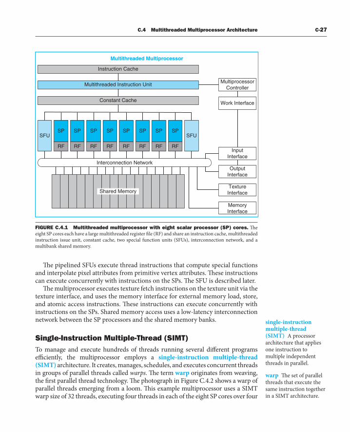
Multiprocessor ArchitectureA unifi ed graphics and computing multiprocessor executes vertex, geometry, and pixel fragment shader programs, and parallel computing programs. As Figure C.4.1 shows, the example multiprocessor consists of eight scalar processor (SP) cores each with a large multithreaded register fi le (RF), two special function units (SFUs), a multithreaded instruction unit, an instruction cache, a read-only constant cache, and a shared memory.
Th e 16 KB shared memory holds graphics data buff ers and shared computing data. CUDA variables declared as __shared__ reside in the shared memory. To map the logical graphics pipeline workload through the multiprocessor multiple times, as shown in Section C.2, vertex, geometry, and pixel threads have independent input and output buff ers, and workloads arrive and depart independently of thread execution.
Each SP core contains scalar integer and fl oating-point arithmetic units that execute most instructions. Th e SP is hardware multithreaded, supporting up to 64 threads. Each pipelined SP core executes one scalar instruction per thread per clock, which ranges from 1.2 GHz to 1.6 GHz in diff erent GPU products. Each SP core has a large RF of 1024 general-purpose 32-bit registers, partitioned among its assigned threads. Programs declare their register demand, typically 16 to 64 scalar 32-bit registers per thread. Th e SP can concurrently run many threads that use a few registers or fewer threads that use more registers. Th e compiler optimizes register allocation to balance the cost of spilling registers versus the cost of fewer threads. Pixel shader programs oft en use 16 or fewer registers, enabling each SP to run up to 64 pixel shader threads to cover long-latency texture fetches. Compiled CUDA programs oft en need 32 registers per thread, limiting each SP to 32 threads, which limits such a kernel program to 256 threads per thread block on this example multiprocessor, rather than its maximum of 512 threads.
C.4 Multithreaded Multiprocessor Architecture C-27
Th e pipelined SFUs execute thread instructions that compute special functions and interpolate pixel attributes from primitive vertex attributes. Th ese instructions can execute concurrently with instructions on the SPs. Th e SFU is described later.
Th e multiprocessor executes texture fetch instructions on the texture unit via the texture interface, and uses the memory interface for external memory load, store, and atomic access instructions. Th ese instructions can execute concurrently with instructions on the SPs. Shared memory access uses a low-latency interconnection network between the SP processors and the shared memory banks.
Single-Instruction Multiple-Thread (SIMT)To manage and execute hundreds of threads running several diff erent programs effi ciently, the multiprocessor employs a single-instruction multiple-thread (SIMT) architecture. It creates, manages, schedules, and executes concurrent threads in groups of parallel threads called warps. Th e term warp originates from weaving, the fi rst parallel thread technology. Th e photograph in Figure C.4.2 shows a warp of parallel threads emerging from a loom. Th is example multiprocessor uses a SIMT warp size of 32 threads, executing four threads in each of the eight SP cores over four
single-instruction multiple-thread (SIMT) A processor architecture that applies one instruction to multiple independent threads in parallel.
warp Th e set of parallel threads that execute the same instruction together in a SIMT architecture.
Instruction Cache
Multithreaded Instruction Unit
Multithreaded Multiprocessor
Constant Cache
SFU SFUSP
RF
SP
RF
SP
RF
SP
RF
SP
RF
SP
RF
SP
RF
SP
RF
Shared MemoryTextureInterface
MemoryInterface
MultiprocessorController
OutputInterface
Interconnection Network
InputInterface
Work Interface
FIGURE C.4.1 Multithreaded multiprocessor with eight scalar processor (SP) cores. Th e eight SP cores each have a large multithreaded register fi le (RF) and share an instruction cache, multithreaded instruction issue unit, constant cache, two special function units (SFUs), interconnection network, and a multibank shared memory.

C-28 Appendix C Graphics and Computing GPUs
clocks. Th e Tesla SM multiprocessor described in Section C.7 also uses a warp size of 32 parallel threads, executing four threads per SP core for effi ciency on plentiful pixel threads and computing threads. Th read blocks consist of one or more warps.
Th is example SIMT multiprocessor manages a pool of 16 warps, a total of 512 threads. Individual parallel threads composing a warp are the same type and start together at the same program address, but are otherwise free to branch and execute independently. At each instruction issue time, the SIMT multithreaded instruction unit selects a warp that is ready to execute its next instruction, and then issues that instruction to the active threads of that warp. A SIMT instruction is broadcast synchronously to the active parallel threads of a warp; individual threads may be inactive due to independent branching or predication. In this multiprocessor, each SP scalar processor core executes an instruction for four individual threads of a warp using four clocks, refl ecting the 4:1 ratio of warp threads to cores.
SIMT processor architecture is akin to single-instruction multiple data (SIMD) design, which applies one instruction to multiple data lanes, but diff ers in that SIMT applies one instruction to multiple independent threads in parallel, not just
warp 8 instruction 11
warp 1 instruction 42
warp 3 instruction 95
warp 8 instruction 12
time
SIMT multithreadedinstruction scheduler
warp 1 instruction 43
warp 3 instruction 96
Pho
to: J
udy
Sch
oonm
aker
FIGURE C.4.2 SIMT multithreaded warp scheduling. Th e scheduler selects a ready warp and issues an instruction synchronously to the parallel threads composing the warp. Because warps are independent, the scheduler may select a diff erent warp each time.

C.4 Multithreaded Multiprocessor Architecture C-29
to multiple data lanes. An instruction for a SIMD processor controls a vector of multiple data lanes together, whereas an instruction for a SIMT processor controls an individual thread, and the SIMT instruction unit issues an instruction to a warp of independent parallel threads for effi ciency. Th e SIMT processor fi nds data-level parallelism among threads at runtime, analogous to the way a superscalar processor fi nds instruction-level parallelism among instructions at runtime.
A SIMT processor realizes full effi ciency and performance when all threads of a warp take the same execution path. If threads of a warp diverge via a data-dependent conditional branch, execution serializes for each branch path taken, and when all paths complete, the threads converge to the same execution path. For equal length paths, a divergent if-else code block is 50% effi cient. Th e multiprocessor uses a branch synchronization stack to manage independent threads that diverge and converge. Diff erent warps execute independently at full speed regardless of whether they are executing common or disjoint code paths. As a result, SIMT GPUs are dramatically more effi cient and fl exible on branching code than earlier GPUs, as their warps are much narrower than the SIMD width of prior GPUs.
In contrast with SIMD vector architectures, SIMT enables programmers to write thread-level parallel code for individual independent threads, as well as data-parallel code for many coordinated threads. For program correctness, the programmer can essentially ignore the SIMT execution attributes of warps; however, substantial performance improvements can be realized by taking care that the code seldom requires threads in a warp to diverge. In practice, this is analogous to the role of cache lines in traditional codes: cache line size can be safely ignored when designing for correctness but must be considered in the code structure when designing for peak performance.
SIMT Warp Execution and DivergenceTh e SIMT approach of scheduling independent warps is more fl exible than the scheduling of previous GPU architectures. A warp comprises parallel threads of the same type: vertex, geometry, pixel, or compute. Th e basic unit of pixel fragment shader processing is the 2-by-2 pixel quad implemented as four pixel shader threads. Th e multiprocessor controller packs the pixel quads into a warp. It similarly groups vertices and primitives into warps, and packs computing threads into a warp. A thread block comprises one or more warps. Th e SIMT design shares the instruction fetch and issue unit effi ciently across parallel threads of a warp, but requires a full warp of active threads to get full performance effi ciency.
Th is unifi ed multiprocessor schedules and executes multiple warp types concurrently, allowing it to concurrently execute vertex and pixel warps. Its warp scheduler operates at less than the processor clock rate, because there are four thread lanes per processor core. During each scheduling cycle, it selects a warp to execute a SIMT warp instruction, as shown in Figure C.4.2. An issued warp-instruction executes as four sets of eight threads over four processor cycles of throughput. Th e processor pipeline uses several clocks of latency to complete each instruction. If the number of active warps times the clocks per warp exceeds the pipeline latency, the
C-30 Appendix C Graphics and Computing GPUs
programmer can ignore the pipeline latency. For this multiprocessor, a round-robin schedule of eight warps has a period of 32 cycles between successive instructions for the same warp. If the program can keep 256 threads active per multiprocessor, instruction latencies up to 32 cycles can be hidden from an individual sequential thread. However, with few active warps, the processor pipeline depth becomes visible and may cause processors to stall.
A challenging design problem is implementing zero-overhead warp scheduling for a dynamic mix of diff erent warp programs and program types. Th e instruction scheduler must select a warp every four clocks to issue one instruction per clock per thread, equivalent to an IPC of 1.0 per processor core. Because warps are independent, the only dependences are among sequential instructions from the same warp. Th e scheduler uses a register dependency scoreboard to qualify warps whose active threads are ready to execute an instruction. It prioritizes all such ready warps and selects the highest priority one for issue. Prioritization must consider warp type, instruction type, and the desire to be fair to all active warps.
Managing Threads and Thread BlocksTh e multiprocessor controller and instruction unit manage threads and thread blocks. Th e controller accepts work requests and input data and arbitrates access to shared resources, including the texture unit, memory access path, and I/O paths. For graphics workloads, it creates and manages three types of graphics threads concurrently: vertex, geometry, and pixel. Each of the graphics work types has independent input and output paths. It accumulates and packs each of these input work types into SIMT warps of parallel threads executing the same thread program. It allocates a free warp, allocates registers for the warp threads, and starts warp execution in the multiprocessor. Every program declares its per-thread register demand; the controller starts a warp only when it can allocate the requested register count for the warp threads. When all the threads of the warp exit, the controller unpacks the results and frees the warp registers and resources.
Th e controller creates cooperative thread arrays (CTAs) which implement CUDA thread blocks as one or more warps of parallel threads. It creates a CTA when it can create all CTA warps and allocate all CTA resources. In addition to threads and registers, a CTA requires allocating shared memory and barriers. Th e program declares the required capacities, and the controller waits until it can allocate those amounts before launching the CTA. Th en it creates CTA warps at the warp scheduling rate, so that a CTA program starts executing immediately at full multiprocessor performance. Th e controller monitors when all threads of a CTA have exited, and frees the CTA shared resources and its warp resources.
Thread InstructionsTh e SP thread processors execute scalar instructions for individual threads, unlike earlier GPU vector instruction architectures, which executed four-component vector instructions for each vertex or pixel shader program. Vertex programs
cooperative thread array (CTA) A set of concurrent threads that executes the same thread program and may cooperate to compute a result. A GPU CTA implements a CUDA thread block.

C.4 Multithreaded Multiprocessor Architecture C-31
generally compute (x, y, z, w) position vectors, while pixel shader programs compute (red, green, blue, alpha) color vectors. However, shader programs are becoming longer and more scalar, and it is increasingly diffi cult to fully occupy even two components of a legacy GPU four-component vector architecture. In eff ect, the SIMT architecture parallelizes across 32 independent pixel threads, rather than parallelizing the four vector components within a pixel. CUDA C/C�� programs have predominantly scalar code per thread. Previous GPUs employed vector packing (e.g., combining subvectors of work to gain effi ciency) but that complicated the scheduling hardware as well as the compiler. Scalar instructions are simpler and compiler friendly. Texture instructions remain vector based, taking a source coordinate vector and returning a fi ltered color vector.
To support multiple GPUs with diff erent binary microinstruction formats, high-level graphics and computing language compilers generate intermediate assembler-level instructions (e.g., Direct3D vector instructions or PTX scalar instructions), which are then optimized and translated to binary GPU microinstructions. Th e NVIDIA PTX (parallel thread execution) instruction set defi nition [2007] provides a stable target ISA for compilers, and provides compatibility over several generations of GPUs with evolving binary microinstruction-set architectures. Th e optimizer readily expands Direct3D vector instructions to multiple scalar binary microinstructions. PTX scalar instructions translate nearly one to one with scalar binary microinstructions, although some PTX instructions expand to multiple binary microinstructions, and multiple PTX instructions may fold into one binary microinstruction. Because the intermediate assembler-level instructions use virtual registers, the optimizer analyzes data dependencies and allocates real registers. Th e optimizer eliminates dead code, folds instructions together when feasible, and optimizes SIMT branch diverge and converge points.
Instruction Set Architecture (ISA)Th e thread ISA described here is a simplifi ed version of the Tesla architecture PTX ISA, a register-based scalar instruction set comprising fl oating-point, integer, logical, conversion, special functions, fl ow control, memory access, and texture operations. Figure C.4.3 lists the basic PTX GPU thread instructions; see the NVIDIA PTX specifi cation [2007] for details. Th e instruction format is:
opcode.type d, a, b, c;
where d is the destination operand, a, b, c are source operands, and .type is one of:
Type .type Specifer
Untyped bits 8, 16, 32, and 64 bits .b8, .b16, .b32, .b64
Unsigned integer 8, 16, 32, and 64 bits .u8, .u16, .u32, .u64
Signed integer 8, 16, 32, and 64 bits .s8, .s16, .s32, .s64
Floating-point 16, 32, and 64 bits .f16, .f32, .f64

C-32 Appendix C Graphics and Computing GPUs
FIGURE C.4.3 Basic PTX GPU thread instructions.
Basic PTX GPU Thread Instructions
Group Instruction Example Meaning Comments
Arithmetic
arithmetic .type = .s32, .u32, .f32, .s64, .u64, .f64add.type add.f32 d, a, b d = a + b;sub.type sub.f32 d, a, b d = a – b;mul.type mul.f32 d, a, b d = a * b;mad.type mad.f32 d, a, b, c d = a * b + c; multiply-add
div.type div.f32 d, a, b d = a / b; multiple microinstructions
rem.type rem.u32 d, a, b d = a % b; integer remainder
abs.type abs.f32 d, a d = |a|;neg.type neg.f32 d, a d = 0 - a;min.type min.f32 d, a, b d = (a < b)? a:b; floating selects non-NaN
max.type max.f32 d, a, b d = (a > b)? a:b; floating selects non-NaN
setp.cmp.type setp.lt.f32 p, a, b p = (a < b); compare and set predicate
numeric .cmp = eq, ne, lt, le, gt, ge; unordered cmp = equ, neu, ltu, leu, gtu, geu, num, nan
mov.type mov.b32 d, a d = a; move
selp.type selp.f32 d, a, b, p d = p? a: b; select with predicate
cvt.dtype.atype cvt.f32.s32 d, a d = convert(a); convert atype to dtype
Special Function
special .type = .f32 (some .f64)
rcp.type rcp.f32 d, a d = 1/a; reciprocal
sqrt.type sqrt.f32 d, a d = sqrt(a); square root
rsqrt.type rsqrt.f32 d, a d = 1/sqrt(a); reciprocal square root
sin.type sin.f32 d, a d = sin(a); sine
cos.type cos.f32 d, a d = cos(a); cosine
lg2.type lg2.f32 d, a d = log(a)/log(2) binary logarithm
ex2.type ex2.f32 d, a d = 2 ** a; binary exponential
Logical
logic. type = .pred, .b32, .b64and.type and.b32 d, a, b d = a & b;or.type or.b32 d, a, b d = a | b;xor.type xor.b32 d, a, b d = a ^ b;not.type not.b32 d, a, b d = ~a; one’s complement
cnot.type cnot.b32 d, a, b d = (a==0)? 1:0; C logical not
shl.type shl.b32 d, a, b d = a << b; shift left
shr.type shr.s32 d, a, b d = a >> b; shift right
MemoryAccess
memory .space = .global, .shared, .local, .const; .type = .b8, .u8, .s8, .b16, .b32, .b64ld.space.type ld.global.b32 d, [a+off] d = *(a+off); load from memory space
st.space.type st.shared.b32 [d+off], a *(d+off) = a; store to memory space
tex.nd.dtyp.btype tex.2d.v4.f32.f32 d, a, b d = tex2d(a, b); texture lookup
atom.spc.op.type atom.global.add.u32 d,[a], b atom.global.cas.b32 d,[a], b, c
atomic { d = *a; *a = op(*a, b); }
atomic read-modify-write operation
atom .op = and, or, xor, add, min, max, exch, cas; .spc = .global; .type = .b32
ControlFlow
branch @p bra target if (p) goto target;
conditional branch
call call (ret), func, (params) ret = func(params); call function
ret ret return; return from function call
bar.sync bar.sync d wait for threads barrier synchronization
exit exit exit; terminate thread execution
C.4 Multithreaded Multiprocessor Architecture C-33
Source operands are scalar 32-bit or 64-bit values in registers, an immediate value, or a constant; predicate operands are 1-bit Boolean values. Destinations are registers, except for store to memory. Instructions are predicated by prefi xing them with @p or @!p, where p is a predicate register. Memory and texture instructions transfer scalars or vectors of two to four components, up to 128 bits in total. PTX instructions specify the behavior of one thread.
Th e PTX arithmetic instructions operate on 32-bit and 64-bit fl oating-point, signed integer, and unsigned integer types. Recent GPUs support 64-bit double precision fl oating-point; see Section C.6. On current GPUs, PTX 64-bit integer and logical instructions are translated to two or more binary microinstructions that perform 32-bit operations. Th e GPU special function instructions are limited to 32-bit fl oating-point. Th e thread control fl ow instructions are conditional branch, function call and return, thread exit, and bar.sync (barrier synchronization). Th e conditional branch instruction @p bra target uses a predicate register p (or !p) previously set by a compare and set predicate setp instruction to determine whether the thread takes the branch or not. Other instructions can also be predicated on a predicate register being true or false.
Memory Access Instructions
Th e tex instruction fetches and fi lters texture samples from 1D, 2D, and 3D texture arrays in memory via the texture subsystem. Texture fetches generally use interpolated fl oating-point coordinates to address a texture. Once a graphics pixel shader thread computes its pixel fragment color, the raster operations processor blends it with the pixel color at its assigned (x, y) pixel position and writes the fi nal color to memory.
To support computing and C/C�� language needs, the Tesla PTX ISA implements memory load/store instructions. It uses integer byte addressing with register plus off set address arithmetic to facilitate conventional compiler code optimizations. Memory load/store instructions are common in processors, but are a signifi cant new capability in the Tesla architecture GPUs, as prior GPUs provided only the texture and pixel accesses required by the graphics APIs.
For computing, the load/store instructions access three read/write memory spaces that implement the corresponding CUDA memory spaces in Section C.3:
■ Local memory for per-thread private addressable temporary data (implemented in external DRAM)
■ Shared memory for low-latency access to data shared by cooperating threads in the same CTA/thread block (implemented in on-chip SRAM)
■ Global memory for large data sets shared by all threads of a computing application (implemented in external DRAM)
Th e memory load/store instructions ld.global, st.global, ld.shared, st.shared, ld.local, and st.local access the global, shared, and local memory spaces. Computing programs use the fast barrier synchronization instruction bar.sync to synchronize threads within a CTA/thread block that communicate with each other via shared and global memory.

C-34 Appendix C Graphics and Computing GPUs
To improve memory bandwidth and reduce overhead, the local and global load/store instructions coalesce individual parallel thread requests from the same SIMT warp together into a single memory block request when the addresses fall in the same block and meet alignment criteria. Coalescing memory requests provides a signifi cant performance boost over separate requests from individual threads. Th e multiprocessor’s large thread count, together with support for many outstanding load requests, helps cover load-to-use latency for local and global memory implemented in external DRAM.
Th e latest Tesla architecture GPUs also provide effi cient atomic memory operations on memory with the atom.op.u32 instructions, including integer operations add, min, max, and, or, xor, exchange, and cas (compare-and-swap) operations, facilitating parallel reductions and parallel data structure management.
Barrier Synchronization for Thread Communication
Fast barrier synchronization permits CUDA programs to communicate frequently via shared memory and global memory by simply calling __syncthreads(); as part of each interthread communication step. Th e synchronization intrinsic function generates a single bar.sync instruction. However, implementing fast barrier synchronization among up to 512 threads per CUDA thread block is a challenge.
Grouping threads into SIMT warps of 32 threads reduces the synchronization diffi culty by a factor of 32. Th reads wait at a barrier in the SIMT thread scheduler so they do not consume any processor cycles while waiting. When a thread executes a bar.sync instruction, it increments the barrier’s thread arrival counter and the scheduler marks the thread as waiting at the barrier. Once all the CTA threads arrive, the barrier counter matches the expected terminal count, and the scheduler releases all the threads waiting at the barrier and resumes executing threads.
Streaming Processor (SP)Th e multithreaded streaming processor (SP) core is the primary thread instruction processor in the multiprocessor. Its register fi le (RF) provides 1024 scalar 32-bit registers for up to 64 threads. It executes all the fundamental fl oating-point operations, including add.f32, mul.f32, mad.f32 (fl oating multiply-add), min.f32, max.f32, and setp.f32 (fl oating compare and set predicate). Th e fl oating-point add and multiply operations are compatible with the IEEE 754 standard for single precision FP numbers, including not-a-number (NaN) and infi nity values. Th e SP core also implements all of the 32-bit and 64-bit integer arithmetic, comparison, conversion, and logical PTX instructions shown in Figure C.4.3.
Th e fl oating-point add and mul operations employ IEEE round-to-nearest-even as the default rounding mode. Th e mad.f32 fl oating-point multiply-add operation performs a multiplication with truncation, followed by an addition with round-to-nearest-even. Th e SP fl ushes input denormal operands to sign-preserved-zero. Results that underfl ow the target output exponent range are fl ushed to sign-preserved-zero aft er rounding.

C.4 Multithreaded Multiprocessor Architecture C-35
Special Function Unit (SFU)Certain thread instructions can execute on the SFUs, concurrently with other thread instructions executing on the SPs. Th e SFU implements the special function instructions of Figure C.4.3, which compute 32-bit fl oating-point approximations to reciprocal, reciprocal square root, and key transcendental functions. It also implements 32-bit fl oating-point planar attribute interpolation for pixel shaders, providing accurate interpolation of attributes such as color, depth, and texture coordinates.
Each pipelined SFU generates one 32-bit fl oating-point special function result per cycle; the two SFUs per multiprocessor execute special function instructions at a quarter the simple instruction rate of the eight SPs. Th e SFUs also execute the mul.f32 multiply instruction concurrently with the eight SPs, increasing the peak computation rate up to 50% for threads with a suitable instruction mixture.
For functional evaluation, the Tesla architecture SFU employs quadratic interpolation based on enhanced minimax approximations for approximating the reciprocal, reciprocal square-root, log2x, 2x, and sin/cos functions. Th e accuracy of the function estimates ranges from 22 to 24 mantissa bits. See Section C.6 for more details on SFU arithmetic.
Comparing with Other MultiprocessorsCompared with SIMD vector architectures such as x86 SSE, the SIMT multiprocessor can execute individual threads independently, rather than always executing them together in synchronous groups. SIMT hardware fi nds data parallelism among independent threads, whereas SIMD hardware requires the soft ware to express data parallelism explicitly in each vector instruction. A SIMT machine executes a warp of 32 threads synchronously when the threads take the same execution path, yet can execute each thread independently when they diverge. Th e advantage is signifi cant because SIMT programs and instructions simply describe the behavior of a single independent thread, rather than a SIMD data vector of four or more data lanes. Yet the SIMT multiprocessor has SIMD-like effi ciency, spreading the area and cost of one instruction unit across the 32 threads of a warp and across the eight streaming processor cores. SIMT provides the performance of SIMD together with the productivity of multithreading, avoiding the need to explicitly code SIMD vectors for edge conditions and partial divergence.
Th e SIMT multiprocessor imposes little overhead because it is hardware multithreaded with hardware barrier synchronization. Th at allows graphics shaders and CUDA threads to express very fi ne-grained parallelism. Graphics and CUDA programs use threads to express fi ne-grained data parallelism in a per-thread program, rather than forcing the programmer to express it as SIMD vector instructions. It is simpler and more productive to develop scalar single-thread code than vector code, and the SIMT multiprocessor executes the code with SIMD-like effi ciency.

C-36 Appendix C Graphics and Computing GPUs
Coupling eight streaming processor cores together closely into a multiprocessor and then implementing a scalable number of such multiprocessors makes a two-level multiprocessor composed of multiprocessors. Th e CUDA programming model exploits the two-level hierarchy by providing individual threads for fi ne-grained parallel computations, and by providing grids of thread blocks for coarse-grained parallel operations. Th e same thread program can provide both fi ne-grained and coarse-grained operations. In contrast, CPUs with SIMD vector instructions must use two diff erent programming models to provide fi ne-grained and coarse-grained operations: coarse-grained parallel threads on diff erent cores, and SIMD vector instructions for fi ne-grained data parallelism.
Multithreaded Multiprocessor ConclusionTh e example GPU multiprocessor based on the Tesla architecture is highly multithreaded, executing a total of up to 512 lightweight threads concurrently to support fi ne-grained pixel shaders and CUDA threads. It uses a variation on SIMD architecture and multithreading called SIMT (single-instruction multiple-thread) to effi ciently broadcast one instruction to a warp of 32 parallel threads, while permitting each thread to branch and execute independently. Each thread executes its instruction stream on one of the eight streaming processor (SP) cores, which are multithreaded up to 64 threads.
Th e PTX ISA is a register-based load/store scalar ISA that describes the execution of a single thread. Because PTX instructions are optimized and translated to binary microinstructions for a specifi c GPU, the hardware instructions can evolve rapidly without disrupting compilers and soft ware tools that generate PTX instructions.
C.5 Parallel Memory System
Outside of the GPU itself, the memory subsystem is the most important determiner of the performance of a graphics system. Graphics workloads demand very high transfer rates to and from memory. Pixel write and blend (read-modify-write) operations, depth buff er reads and writes, and texture map reads, as well as command and object vertex and attribute data reads, comprise the majority of memory traffi c.
Modern GPUs are highly parallel, as shown in Figure C.2.5. For example, the GeForce 8800 can process 32 pixels per clock, at 600 MHz. Each pixel typically requires a color read and write and a depth read and write of a 4-byte pixel. Usually an average of two or three texels of four bytes each are read to generate the pixel’s color. So for a typical case, there is a demand of 28 bytes times 32 pixels � 896 bytes per clock. Clearly the bandwidth demand on the memory system is enormous.

C.5 Parallel Memory System C-37
To supply these requirements, GPU memory systems have the following characteristics:
■ Th ey are wide, meaning there are a large number of pins to convey data between the GPU and its memory devices, and the memory array itself comprises many DRAM chips to provide the full total data bus width.
■ Th ey are fast, meaning aggressive signaling techniques are used to maximize the data rate (bits/second) per pin.
■ GPUs seek to use every available cycle to transfer data to or from the memory array. To achieve this, GPUs specifi cally do not aim to minimize latency to the memory system. High throughput (utilization effi ciency) and short latency are fundamentally in confl ict.
■ Compression techniques are used, both lossy, of which the programmer must be aware, and lossless, which is invisible to the application and opportunistic.
■ Caches and work coalescing structures are used to reduce the amount of off -chip traffi c needed and to ensure that cycles spent moving data are used as fully as possible.
DRAM ConsiderationsGPUs must take into account the unique characteristics of DRAM. DRAM chips are internally arranged as multiple (typically four to eight) banks, where each bank includes a power-of-2 number of rows (typically around 16,384), and each row contains a power-of-2 number of bits (typically 8192). DRAMs impose a variety of timing requirements on their controlling processor. For example, dozens of cycles are required to activate one row, but once activated, the bits within that row are randomly accessible with a new column address every four clocks. Double-data rate (DDR) synchronous DRAMs transfer data on both rising and falling edges of the interface clock (see Chapter 5). So a 1 GHz clocked DDR DRAM transfers data at 2 gigabits per second per data pin. Graphics DDR DRAMs usually have 32 bidirectional data pins, so eight bytes can be read or written from the DRAM per clock.
GPUs internally have a large number of generators of memory traffi c. Diff erent stages of the logical graphics pipeline each have their own request streams: command and vertex attribute fetch, shader texture fetch and load/store, and pixel depth and color read-write. At each logical stage, there are oft en multiple independent units to deliver the parallel throughput. Th ese are each independent memory requestors. When viewed at the memory system, there are an enormous number of uncorrelated requests in fl ight. Th is is a natural mismatch to the reference pattern preferred by the DRAMs. A solution is for the GPU’s memory controller to maintain separate heaps of traffi c bound for diff erent DRAM banks, and wait until
C-38 Appendix C Graphics and Computing GPUs
enough traffi c for a particular DRAM row is pending before activating that row and transferring all the traffi c at once. Note that accumulating pending requests, while good for DRAM row locality and thus effi cient use of the data bus, leads to longer average latency as seen by the requestors whose requests spend time waiting for others. Th e design must take care that no particular request waits too long, otherwise some processing units can starve waiting for data and ultimately cause neighboring processors to become idle.
GPU memory subsystems are arranged as multiple memory partitions, each of which comprises a fully independent memory controller and one or two DRAM devices that are fully and exclusively owned by that partition. To achieve the best load balance and therefore approach the theoretical performance of n partitions, addresses are fi nely interleaved evenly across all memory partitions. Th e partition interleaving stride is typically a block of a few hundred bytes. Th e number of memory partitions is designed to balance the number of processors and other memory requesters.
CachesGPU workloads typically have very large working sets—on the order of hundreds of megabytes to generate a single graphics frame. Unlike with CPUs, it is not practical to construct caches on chips large enough to hold anything close to the full working set of a graphics application. Whereas CPUs can assume very high cache hit rates (99.9% or more), GPUs experience hit rates closer to 90% and must therefore cope with many misses in fl ight. While a CPU can reasonably be designed to halt while waiting for a rare cache miss, a GPU needs to proceed with misses and hits intermingled. We call this a streaming cache architecture.
GPU caches must deliver very high-bandwidth to their clients. Consider the case of a texture cache. A typical texture unit may evaluate two bilinear interpolations for each of four pixels per clock cycle, and a GPU may have many such texture units all operating independently. Each bilinear interpolation requires four separate texels, and each texel might be a 64-bit value. Four 16-bit components are typical. Th us, total bandwidth is 2 � 4 � 4 � 64 � 2048 bits per clock. Each separate 64-bit texel is independently addressed, so the cache needs to handle 32 unique addresses per clock. Th is naturally favors a multibank and/or multiport arrangement of SRAM arrays.
MMUModern GPUs are capable of translating virtual addresses to physical addresses. On the GeForce 8800, all processing units generate memory addresses in a 40-bit virtual address space. For computing, load and store thread instructions use 32-bit byte addresses, which are extended to a 40-bit virtual address by adding a 40-bit off set. A memory management unit performs virtual to physical address

C.5 Parallel Memory System C-39
translation; hardware reads the page tables from local memory to respond to misses on behalf of a hierarchy of translation lookaside buff ers spread out among the processors and rendering engines. In addition to physical page bits, GPU page table entries specify the compression algorithm for each page. Page sizes range from 4 to 128 kilobytes.
Memory SpacesAs introduced in Section C.3, CUDA exposes diff erent memory spaces to allow the programmer to store data values in the most performance-optimal way. For the following discussion, NVIDIA Tesla architecture GPUs are assumed.
Global memoryGlobal memory is stored in external DRAM; it is not local to any one physical streaming multiprocessor (SM) because it is meant for communication among diff erent CTAs (thread blocks) in diff erent grids. In fact, the many CTAs that reference a location in global memory may not be executing in the GPU at the same time; by design, in CUDA a programmer does not know the relative order in which CTAs are executed. Because the address space is evenly distributed among all memory partitions, there must be a read/write path from any streaming multiprocessor to any DRAM partition.
Access to global memory by diff erent threads (and diff erent processors) is not guaranteed to have sequential consistency. Th read programs see a relaxed memory ordering model. Within a thread, the order of memory reads and writes to the same address is preserved, but the order of accesses to diff erent addresses may not be preserved. Memory reads and writes requested by diff erent threads are unordered. Within a CTA, the barrier synchronization instruction bar.sync can be used to obtain strict memory ordering among the threads of the CTA. Th e membar thread instruction provides a memory barrier/fence operation that commits prior memory accesses and makes them visible to other threads before proceeding. Th reads can also use the atomic memory operations described in Section C.4 to coordinate work on memory they share.
Shared memoryPer-CTA shared memory is only visible to the threads that belong to that CTA, and shared memory only occupies storage from the time a CTA is created to the time it terminates. Shared memory can therefore reside on-chip. Th is approach has many benefi ts. First, shared memory traff c does not need to compete with limited off -chip bandwidth needed for global memory references. Second, it is practical to build very high-bandwidth memory structures on-chip to support the read/write demands of each streaming multiprocessor. In fact, the shared memory is closely coupled to the streaming multiprocessor.

C-40 Appendix C Graphics and Computing GPUs
Each streaming multiprocessor contains eight physical thread processors. During one shared memory clock cycle, each thread processor can process two threads’ worth of instructions, so 16 threads’ worth of shared memory requests must be handled in each clock. Because each thread can generate its own addresses, and the addresses are typically unique, the shared memory is built using 16 independently addressable SRAM banks. For common access patterns, 16 banks are suffi cient to maintain throughput, but pathological cases are possible; for example, all 16 threads might happen to access a diff erent address on one SRAM bank. It must be possible to route a request from any thread lane to any bank of SRAM, so a 16-by-16 interconnection network is required.
Local MemoryPer-thread local memory is private memory visible only to a single thread. Local memory is architecturally larger than the thread’s register fi le, and a program can compute addresses into local memory. To support large allocations of local memory (recall the total allocation is the per-thread allocation times the number of active threads), local memory is allocated in external DRAM.
Although global and per-thread local memory reside off -chip, they are well-suited to being cached on-chip.
Constant MemoryConstant memory is read-only to a program running on the SM (it can be written via commands to the GPU). It is stored in external DRAM and cached in the SM. Because commonly most or all threads in a SIMT warp read from the same address in constant memory, a single address lookup per clock is suffi cient. Th e constant cache is designed to broadcast scalar values to threads in each warp.
Texture MemoryTexture memory holds large read-only arrays of data. Textures for computing have the same attributes and capabilities as textures used with 3D graphics. Although textures are commonly two-dimensional images (2D arrays of pixel values), 1D (linear) and 3D (volume) textures are also available.
A compute program references a texture using a tex instruction. Operands include an identifi er to name the texture, and 1, 2, or 3 coordinates based on the texture dimensionality. Th e fl oating-point coordinates include a fractional portion that specifi es a sample location, oft en in between texel locations. Noninteger coordinates invoke a bilinear weighted interpolation of the four closest values (for a 2D texture) before the result is returned to the program.
Texture fetches are cached in a streaming cache hierarchy designed to optimize throughput of texture fetches from thousands of concurrent threads. Some programs use texture fetches as a way to cache global memory.

C.6 Floating-point Arithmetic C-41
SurfacesSurface is a generic term for a one-dimensional, two-dimensional, or three-dimensional array of pixel values and an associated format. A variety of formats are defi ned; for example, a pixel may be defi ned as four 8-bit RGBA integer components, or four 16-bit fl oating-point components. A program kernel does not need to know the surface type. A tex instruction recasts its result values as fl oating-point, depending on the surface format.
Load/Store AccessLoad/store instructions with integer byte addressing enable the writing and compiling of programs in conventional languages like C and C��. CUDA programs use load/store instructions to access memory.
To improve memory bandwidth and reduce overhead, the local and global load/store instructions coalesce individual parallel thread requests from the same warp together into a single memory block request when the addresses fall in the same block and meet alignment criteria. Coalescing individual small memory requests into large block requests provides a signifi cant performance boost over separate requests. Th e large thread count, together with support for many outstanding load requests, helps cover load-to-use latency for local and global memory implemented in external DRAM.
ROPAs shown in Figure C.2.5, NVIDIA Tesla architecture GPUs comprise a scalable streaming processor array (SPA), which performs all of the GPU’s programmable calculations, and a scalable memory system, which comprises external DRAM control and fi xed function Raster Operation Processors (ROPs) that perform color and depth framebuff er operations directly on memory. Each ROP unit is paired with a specifi c memory partition. ROP partitions are fed from the SMs via an interconnection network. Each ROP is responsible for depth and stencil tests and updates, as well as color blending. Th e ROP and memory controllers cooperate to implement lossless color and depth compression (up to 8:1) to reduce external bandwidth demand. ROP units also perform atomic operations on memory.
C.6 Floating-point Arithmetic
GPUs today perform most arithmetic operations in the programmable processor cores using IEEE 754-compatible single precision 32-bit fl oating-point operations (see Chapter 3). Th e fi xed-point arithmetic of early GPUs was succeeded by 16-bit, 24-bit, and 32-bit fl oating-point, then IEEE 754-compatible 32-bit fl oating-
C-42 Appendix C Graphics and Computing GPUs
point. Some fi xed-function logic within a GPU, such as texture-fi ltering hardware, continues to use proprietary numeric formats. Recent GPUs also provide IEEE 754-compatible double precision 64-bit fl oating-point instructions.
Supported FormatsTh e IEEE 754 standard for fl oating-point arithmetic specifi es basic and storage formats. GPUs use two of the basic formats for computation, 32-bit and 64-bit binary fl oating-point, commonly called single precision and double precision. Th e standard also specifi es a 16-bit binary storage fl oating-point format, half precision. GPUs and the Cg shading language employ the narrow 16-bit half data format for effi cient data storage and movement, while maintaining high dynamic range. GPUs perform many texture fi ltering and pixel blending computations at half precision within the texture fi ltering unit and the raster operations unit. Th e OpenEXR high dynamic-range image fi le format developed by Industrial Light and Magic [2003] uses the identical half format for color component values in computer imaging and motion picture applications.
Basic ArithmeticCommon single precision fl oating-point operations in GPU programmable cores include addition, multiplication, multiply-add, minimum, maximum, compare, set predicate, and conversions between integer and fl oating-point numbers. Floating-point instructions oft en provide source operand modifi ers for negation and absolute value.
Th e fl oating-point addition and multiplication operations of most GPUs today are compatible with the IEEE 754 standard for single precision FP numbers, including not-a-number (NaN) and infi nity values. Th e FP addition and multiplication operations use IEEE round-to-nearest-even as the default rounding mode. To increase fl oating-point instruction throughput, GPUs oft en use a compound multiply-add instruction (mad). Th e multiply-add operation performs FP multiplication with truncation, followed by FP addition with round-to-nearest-even. It provides two fl oating-point operations in one issuing cycle, without requiring the instruction scheduler to dispatch two separate instructions, but the computation is not fused and truncates the product before the addition. Th is makes it diff erent from the fused multiply-add instruction discussed in Chapter 3 and later in this section. GPUs typically fl ush denormalized source operands to sign-preserved zero, and they fl ush results that underfl ow the target output exponent range to sign-preserved zero aft er rounding.
Specialized ArithmeticGPUs provide hardware to accelerate special function computation, attribute interpolation, and texture fi ltering. Special function instructions include cosine,
half precision A 16-bit binary fl oating-point format, with 1 sign bit, 5-bit exponent, 10-bit fraction, and an implied integer bit.
multiply-add (MAD) A single fl oating-point instruction that performs a compound operation: multiplication followed by addition.
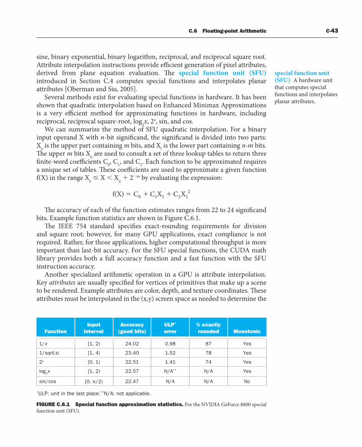
C.6 Floating-point Arithmetic C-43
sine, binary exponential, binary logarithm, reciprocal, and reciprocal square root. Attribute interpolation instructions provide effi cient generation of pixel attributes, derived from plane equation evaluation. Th e special function unit (SFU) introduced in Section C.4 computes special functions and interpolates planar attributes [Oberman and Siu, 2005].
Several methods exist for evaluating special functions in hardware. It has been shown that quadratic interpolation based on Enhanced Minimax Approximations is a very effi cient method for approximating functions in hardware, including reciprocal, reciprocal square-root, log2x, 2x, sin, and cos.
We can summarize the method of SFU quadratic interpolation. For a binary input operand X with n-bit signifi cand, the signifi cand is divided into two parts: Xu is the upper part containing m bits, and Xl is the lower part containing n-m bits. Th e upper m bits Xu are used to consult a set of three lookup tables to return three fi nite-word coeffi cients C0, C1, and C2. Each function to be approximated requires a unique set of tables. Th ese coeffi cients are used to approximate a given function f(X) in the range Xu � X � Xu � 2�m by evaluating the expression:
f(X) C C X C X0 1 1 2 12
Th e accuracy of each of the function estimates ranges from 22 to 24 signifi cand bits. Example function statistics are shown in Figure C.6.1.
Th e IEEE 754 standard specifi es exact-rounding requirements for division and square root; however, for many GPU applications, exact compliance is not required. Rather, for those applications, higher computational throughput is more important than last-bit accuracy. For the SFU special functions, the CUDA math library provides both a full accuracy function and a fast function with the SFU instruction accuracy.
Another specialized arithmetic operation in a GPU is attribute interpolation. Key attributes are usually specifi ed for vertices of primitives that make up a scene to be rendered. Example attributes are color, depth, and texture coordinates. Th ese attributes must be interpolated in the (x,y) screen space as needed to determine the
special function unit (SFU) A hardware unit that computes special functions and interpolates planar attributes.
FunctionInput
intervalAccuracy
(good bits)ULP*
error% exactly rounded Monotonic
1/x [1, 2) 24.02 0.98 87 Yes
1/sqrt(x) [1, 4) 23.40 1.52 78 Yes
2x [0, 1) 22.51 1.41 74 Yes
log2x [1, 2) 22.57 N/A** N/A Yes
sin/cos [0, /2) 22.47 N/A N/A No
*ULP: unit in the last place. **N/A: not applicable.
FIGURE C.6.1 Special function approximation statistics. For the NVIDIA GeForce 8800 special function unit (SFU).

C-44 Appendix C Graphics and Computing GPUs
values of the attributes at each pixel location. Th e value of a given attribute U in an (x, y) plane can be expressed using plane equations of the form:
U(x y) A x B y Cu u u,
where A, B, and C are interpolation parameters associated with each attribute U. Th e interpolation parameters A, B, and C are all represented as single precision fl oating-point numbers.
Given the need for both a function evaluator and an attribute interpolator in a pixel shader processor, a single SFU that performs both functions for effi ciency can be designed. Both functions use a sum of products operation to interpolate results, and the number of terms to be summed in both functions is very similar.
Texture Operations
Texture mapping and fi ltering is another key set of specialized fl oating-point arithmetic operations in a GPU. Th e operations used for texture mapping include:
1. Receive texture address (s, t) for the current screen pixel (x, y), where s and t are single precision fl oating-point numbers.
2. Compute the level of detail to identify the correct texture MIP-map level.
3. Compute the trilinear interpolation fraction.
4. Scale texture address (s, t) for the selected MIP-map level.
5. Access memory and retrieve desired texels (texture elements).
6. Perform fi ltering operation on texels.
Texture mapping requires a signifi cant amount of fl oating-point computation for full-speed operation, much of which is done at 16-bit half precision. As an example, the GeForce 8800 Ultra delivers about 500 GFLOPS of proprietary format fl oating-point computation for texture mapping instructions, in addition to its conventional IEEE single precision fl oating-point instructions. For more details on texture mapping and fi ltering, see Foley and van Dam [1995].
PerformanceTh e fl oating-point addition and multiplication arithmetic hardware is fully pipelined, and latency is optimized to balance delay and area. While pipelined, the throughput of the special functions is less than the fl oating-point addition and multiplication operations. Quarter-speed throughput for the special functions is typical performance in modern GPUs, with one SFU shared by four SP cores. In contrast, CPUs typically have signifi cantly lower throughput for similar functions, such as division and square root, albeit with more accurate results. Th e attribute interpolation hardware is typically fully pipelined to enable full-speed pixel shaders.
MIP-map A Latin phrase multum in parvo, or much in a small space. A MIP-map contains precalculated images of diff erent resolutions, used to increase rendering speed and reduce artifacts.

C.6 Floating-point Arithmetic C-45
Double precisionNewer GPUs such as the Tesla T10P also support IEEE 754 64-bit double precision operations in hardware. Standard fl oating-point arithmetic operations in double precision include addition, multiplication, and conversions between diff erent fl oating-point and integer formats. Th e 2008 IEEE 754 fl oating-point standard includes specifi cation for the fused-multiply-add (FMA) operation, as discussed in Chapter 3. Th e FMA operation performs a fl oating-point multiplication followed by an addition, with a single rounding. Th e fused multiplication and addition operations retain full accuracy in intermediate calculations. Th is behavior enables more accurate fl oating-point computations involving the accumulation of products, including dot products, matrix multiplication, and polynomial evaluation. Th e FMA instruction also enables effi cient soft ware implementations of exactly rounded division and square root, removing the need for a hardware division or square root unit.
A double precision hardware FMA unit implements 64-bit addition, multiplication, conversions, and the FMA operation itself. Th e architecture of a
Multiplier Array53 x 53 Exp
Diff
B CA
Carry Propagate Adder
64
Alignmentshifter
Inversion
3-2 CSA 161 bits
Complementer
Normalizer
Rounder
53
Sum Carry ShiftedC
161
64 64
53 53
Sum Carry
FIGURE C.6.2 Double precision fused-multiply-add (FMA) unit. Hardware to implement fl oating-point A � B � C for double precision.

C-46 Appendix C Graphics and Computing GPUs
double precision FMA unit enables full-speed denormalized number support on both inputs and outputs. Figure C.6.2 shows a block diagram of an FMA unit.
As shown in Figure C.6.2, the signifi cands of A and B are multiplied to form a 106-bit product, with the results left in carry-save form. In parallel, the 53-bit addend C is conditionally inverted and aligned to the 106-bit product. Th e sum and carry results of the 106-bit product are summed with the aligned addend through a 161-bit-wide carry-save adder (CSA). Th e carry-save output is then summed together in a carry-propagate adder to produce an unrounded result in nonredundant, two’s complement form. Th e result is conditionally recomplemented, so as to return a result in sign-magnitude form. Th e complemented result is normalized, and then it is rounded to fi t within the target format.
C.7 Real Stuff: The NVIDIA GeForce 8800
Th e NVIDIA GeForce 8800 GPU, introduced in November 2006, is a unifi ed vertex and pixel processor design that also supports parallel computing applications written in C using the CUDA parallel programming model. It is the fi rst implementation of the Tesla unifi ed graphics and computing architecture described in Section C.4 and in Lindholm et al. [2008]. A family of Tesla architecture GPUs addresses the diff erent needs of laptops, desktops, workstations, and servers.
Streaming Processor Array (SPA)Th e GeForce 8800 GPU shown in Figure C.7.1 contains 128 streaming processor (SP) cores organized as 16 streaming multiprocessors (SMs). Two SMs share a texture unit in each texture/processor cluster (TPC). An array of eight TPCs makes up the streaming processor array (SPA), which executes all graphics shader programs and computing programs.
Th e host interface unit communicates with the host CPU via the PCI-Express bus, checks command consistency, and performs context switching. Th e input assembler collects geometric primitives (points, lines, triangles). Th e work distribution blocks dispatch vertices, pixels, and compute thread arrays to the TPCs in the SPA. Th e TPCs execute vertex and geometry shader programs and computing programs. Output geometric data is sent to the viewport/clip/setup/raster/zcull block to be rasterized into pixel fragments that are then redistributed back into the SPA to execute pixel shader programs. Shaded pixels are sent across the interconnection network for processing by the ROP units. Th e network also routes texture memory read requests from the SPA to DRAM and reads data from DRAM through a level-2 cache back to the SPA.

C.7 Real Stuff: The NVIDIA GeForce 8800 C-47
Texture/Processor Cluster (TPC)Each TPC contains a geometry controller, an SMC, two SMs, and a texture unit as shown in Figure C.7.2.
Th e geometry controller maps the logical graphics vertex pipeline into recir-culation on the physical SMs by directing all primitive and vertex attribute and topology fl ow in the TPC.
Th e SMC controls multiple SMs, arbitrating the shared texture unit, load/store path, and I/O path. Th e SMC serves three graphics workloads simultaneously: vertex, geometry, and pixel.
Th e texture unit processes a texture instruction for one vertex, geometry, or pixel quad, or four compute threads per cycle. Texture instruction sources are texture coordinates, and the outputs are weighted samples, typically a four-component (RGBA) fl oating-point color. Th e texture unit is deeply pipelined. Although it contains a streaming cache to capture fi ltering locality, it streams hits mixed with misses without stalling.
GPU
Host CPU System Memory
DRAM DRAM DRAM DRAM DRAM DRAM
ROP L2 ROP L2 ROP L2 ROP L2 ROP L2 ROP L2
TPC
SPA
TPC TPC TPC TPC TPC TPC TPC
Texture UnitTex L1
Texture UnitTex L1
Texture UnitTex L1
Texture UnitTex L1
Texture UnitTex L1
Texture UnitTex L1
Texture UnitTex L1
Texture UnitTex L1
SM SM SM SM SM SM SM SM SM SM SM SM SM SM SM SM
SP SP SP SP
SP SP SP SP
SP SP SP SP
SP SP SP SP
SP SP SP SP
SP SP SP SP
SP SP SP SP
SP SP SP SP
SP SP SP SP
SP SP SP SP
SP SP SP SP
SP SP SP SP
SP SP SP SP
SP SP SP SP
SP SP SP SP
SP SP SP SP
SP SP SP SP
SP SP SP SP
SP SP SP SP
SP SP SP SP
SP SP SP SP
SP SP SP SP
SP SP SP SP
SP SP SP SP
SP SP SP SP
SP SP SP SP
SP SP SP SP
SP SP SP SP
SP SP SP SP
SP SP SP SP
SP SP SP SP
SP SP SP SP
Vertex WorkDistribution
Input Assembler
Host Interface
Bridge
Pixel WorkDistribution
Viewport/Clip/Setup/Raster/
ZCull
Compute WorkDistribution
Interconnection Network
Interface
Display
High-DefinitionVideo Processors
SharedMemory
SharedMemory
SharedMemory
SharedMemory
SharedMemory
SharedMemory
SharedMemory
SharedMemory
SharedMemory
SharedMemory
SharedMemory
SharedMemory
SharedMemory
SharedMemory
SharedMemory
SharedMemory
FIGURE C.7.1 NVIDIA Tesla unifi ed graphics and computing GPU architecture. Th is GeForce 8800 has 128 streaming processor (SP) cores in 16 streaming multiprocessors (SMs), arranged in eight texture/processor clusters (TPCs). Th e processors connect with six 64-bit-wide DRAM partitions via an interconnection network. Other GPUs implementing the Tesla architecture vary the number of SP cores, SMs, DRAM partitions, and other units.

C-48 Appendix C Graphics and Computing GPUs
Streaming Multiprocessor (SM)Th e SM is a unifi ed graphics and computing multiprocessor that executes vertex, geometry, and pixel-fragment shader programs and parallel computing programs. Th e SM consists of eight SP thread processor cores, two SFUs, a multithreaded instruction fetch and issue unit (MT issue), an instruction cache, a read-only constant cache, and a 16 KB read/write shared memory. It executes scalar instructions for individual threads.
Th e GeForce 8800 Ultra clocks the SP cores and SFUs at 1.5 GHz, for a peak of 36 GFLOPS per SM. To optimize power and area effi ciency, some SM nondatapath units operate at half the SP clock rate.
SMC
Geometry Controller
TPC
Texture Unit
Tex L1
SP
SharedMemory
SP
SP SP
SP SP
SP SP
I-Cache
MT Issue
C-Cache
SFU SFU
SP
SharedMemory
SP
SP SP
SP SP
SP SP
I-Cache
MT Issue
C-Cache
SFU SFU
SharedMemory
I-Cache
MT Issue
C-Cache
SFU SFU
SM
SM SM
SP
SP
SP
SP SP
SP
SP
SP
FIGURE C.7.2 Texture/processor cluster (TPC) and a streaming multiprocessor (SM). Each SM has eight streaming processor (SP) cores, two SFUs, and a shared memory.
C.7 Real Stuff: The NVIDIA GeForce 8800 C-49
To effi ciently execute hundreds of parallel threads while running several diff erent programs, the SM is hardware multithreaded. It manages and executes up to 768 concurrent threads in hardware with zero scheduling overhead. Each thread has its own thread execution state and can execute an independent code path.
A warp consists of up to 32 threads of the same type—vertex, geometry, pixel, or compute. Th e SIMT design, previously described in Section C.4, shares the SM instruction fetch and issue unit effi ciently across 32 threads but requires a full warp of active threads for full performance effi ciency.
Th e SM schedules and executes multiple warp types concurrently. Each issue cycle, the scheduler selects one of the 24 warps to execute a SIMT warp instruction. An issued warp instruction executes as four sets of 8 threads over four processor cycles. Th e SP and SFU units execute instructions independently, and by issuing instructions between them on alternate cycles, the scheduler can keep both fully occupied. A scoreboard qualifi es each warp for issue each cycle. Th e instruction scheduler prioritizes all ready warps and selects the one with highest priority for issue. Prioritization considers warp type, instruction type, and “fairness” to all warps executing in the SM.
Th e SM executes cooperative thread arrays (CTAs) as multiple concurrent warps which access a shared memory region allocated dynamically for the CTA.
Instruction SetTh reads execute scalar instructions, unlike previous GPU vector instruction architectures. Scalar instructions are simpler and compiler friendly. Texture instructions remain vector based, taking a source coordinate vector and returning a fi ltered color vector.
Th e register-based instruction set includes all the fl oating-point and integer arithmetic, transcendental, logical, fl ow control, memory load/store, and texture instructions listed in the PTX instruction table of Figure C.4.3. Memory load/store instructions use integer byte addressing with register-plus-off set address arithmetic. For computing, the load/store instructions access three read-write memory spaces: local memory for per-thread, private, temporary data; shared memory for low-latency per-CTA data shared by the threads of the CTA; and global memory for data shared by all threads. Computing programs use the fast barrier synchronization bar.sync instruction to synchronize threads within a CTA that communicate with each other via shared and global memory. Th e latest Tesla architecture GPUs implement PTX atomic memory operations, which facilitate parallel reductions and parallel data structure management.
Streaming Processor (SP)Th e multithreaded SP core is the primary thread processor, as introduced in Section C.4. Its register fi le provides 1024 scalar 32-bit registers for up to 96 threads (more threads than in the example SP of Section C.4). Its fl oating-point add and

C-50 Appendix C Graphics and Computing GPUs
multiply operations are compatible with the IEEE 754 standard for single precision FP numbers, including not-a-number (NaN) and infi nity. Th e add and multiply operations use IEEE round-to-nearest-even as the default rounding mode. Th e SP core also implements all of the 32-bit and 64-bit integer arithmetic, comparison, conversion, and logical PTX instructions in Figure C.4.3. Th e processor is fully pipelined, and latency is optimized to balance delay and area.
Special Function Unit (SFU)Th e SFU supports computation of both transcendental functions and planar attribute interpolation. As described in Section C.6, it uses quadratic interpolation based on enhanced minimax approximations to approximate the reciprocal, reciprocal square root, log2x, 2x, and sin/cos functions at one result per cycle. Th e SFU also supports pixel attribute interpolation such as color, depth, and texture coordinates at four samples per cycle.
RasterizationGeometry primitives from the SMs go in their original round-robin input order to the viewport/clip/setup/raster/zcull block. Th e viewport and clip units clip the primitives to the view frustum and to any enabled user clip planes, and then transform the vertices into screen (pixel) space.
Surviving primitives then go to the setup unit, which generates edge equations for the rasterizer. A coarse-rasterization stage generates all pixel tiles that are at least partially inside the primitive. Th e zcull unit maintains a hierarchical z surface, rejecting pixel tiles if they are conservatively known to be occluded by previously drawn pixels. Th e rejection rate is up to 256 pixels per clock. Pixels that survive zcull then go to a fi ne-rasterization stage that generates detailed coverage information and depth values.
Th e depth test and update can be performed ahead of the fragment shader, or aft er, depending on current state. Th e SMC assembles surviving pixels into warps to be processed by an SM running the current pixel shader. Th e SMC then sends surviving pixel and associated data to the ROP.
Raster Operations Processor (ROP) and Memory SystemEach ROP is paired with a specifi c memory partition. For each pixel fragment emitted by a pixel shader program, ROPs perform depth and stencil testing and updates, and in parallel, color blending and updates. Lossless color compression (up to 8:1) and depth compression (up to 8:1) are used to reduce DRAM bandwidth. Each ROP has a peak rate of four pixels per clock and supports 16-bit fl oating-point and 32-bit fl oating-point HDR formats. ROPs support double-rate-depth processing when color writes are disabled.
C.7 Real Stuff: The NVIDIA GeForce 8800 C-51
Antialiasing support includes up to 16� multisampling and supersampling. Th e coverage-sampling antialiasing (CSAA) algorithm computes and stores Boolean coverage at up to 16 samples and compresses redundant color, depth, and stencil information into the memory footprint and a bandwidth of four or eight samples for improved performance.
Th e DRAM memory data bus width is 384 pins, arranged in six independent partitions of 64 pins each. Each partition supports double-data-rate DDR2 and graphics-oriented GDDR3 protocols at up to 1.0 GHz, yielding a bandwidth of about 16 GB/s per partition, or 96 GB/s.
Th e memory controllers support a wide range of DRAM clock rates, protocols, device densities, and data bus widths. Texture and load/store requests can occur between any TPC and any memory partition, so an interconnection network routes requests and responses.
ScalabilityTh e Tesla unifi ed architecture is designed for scalability. Varying the number of SMs, TPCs, ROPs, caches, and memory partitions provides the right balance for diff erent performance and cost targets in GPU market segments. Scalable link interconnect (SLI) connects multiple GPUs, providing further scalability.
PerformanceTh e GeForce 8800 Ultra clocks the SP thread processor cores and SFUs at 1.5 GHz, for a theoretical operation peak of 576 GFLOPS. Th e GeForce 8800 GTX has a 1.35 GHz processor clock and a corresponding peak of 518 GFLOPS.
Th e following three sections compare the performance of a GeForce 8800 GPU with a multicore CPU on three diff erent applications—dense linear algebra, fast Fourier transforms, and sorting. Th e GPU programs and libraries are compiled CUDA C code. Th e CPU code uses the single precision multithreaded Intel MKL 10.0 library to leverage SSE instructions and multiple cores.
Dense Linear Algebra PerformanceDense linear algebra computations are fundamental in many applications. Volkov and Demmel [2008] present GPU and CPU performance results for single precision dense matrix-matrix multiplication (the SGEMM routine) and LU, QR, and Cholesky matrix factorizations. Figure C.7.3 compares GFLOPS rates on SGEMM dense matrix-matrix multiplication for a GeForce 8800 GTX GPU with a quad-core CPU. Figure C.7.4 compares GFLOPS rates on matrix factorization for a GPU with a quad-core CPU.
Because SGEMM matrix-matrix multiply and similar BLAS3 routines are the bulk of the work in matrix factorization, their performance sets an upper bound on factorization rate. As the matrix order increases beyond 200 to 400, the factorization

C-52 Appendix C Graphics and Computing GPUs
FIGURE C.7.4 Dense matrix factorization performance rates. Th e graph shows GFLOPS rates achieved in matrix factorizations using the GPU and using the CPU alone. Adapted from Figure 7 of Volkov and Demmel [2008]. Th e black lines are for a 1.35 GHz NVIDIA GeForce 8800 GTX, CUDA 1.1, Windows XP attached to a 2.67 GHz Intel Core2 Duo E6700 Windows XP, including all CPU–GPU data transfer times. Th e blue lines are for a quad-core 2.4 GHz Intel Core2 Quad Q6600, 64-bit Linux, Intel MKL 10.0.
FIGURE C.7.3 SGEMM dense matrix-matrix multiplication performance rates. Th e graph shows single precision GFLOPS rates achieved in multiplying square N�N matrices (solid lines) and thin N�64 and 64�N matrices (dashed lines). Adapted from Figure 6 of Volkov and Demmel [2008]. Th e black lines are a 1.35 GHz GeForce 8800 GTX using Volkov’s SGEMM code (now in NVIDIA CUBLAS 2.0) on matrices in GPU memory. Th e blue lines are a quad-core 2.4 GHz Intel Core2 Quad Q6600, 64-bit Linux, Intel MKL 10.0 on matrices in CPU memory.
210
180
150
120
90
60
30
0
GF
LOP
S
N64 128 256 512 1024 2048 4096 8192
A:N�N, B:N�N A:N�64, B:64�N
GeForce 8800 GTX
Core2 Quad
LU Cholesky QR
Core2 Quad
210
180
150
120
90
60
30
0
Order of Matrix
GF
LOP
S
GeF
orce
880
0 G
TX +
Cor
e2 D
uo
64 128 256 512 1024 2048 4096 8192 16,384

C.7 Real Stuff: The NVIDIA GeForce 8800 C-53
problem becomes large enough that SGEMM can leverage the GPU parallelism and overcome the CPU–GPU system and copy overhead. Volkov’s SGEMM matrix-matrix multiply achieves 206 GFLOPS, about 60% of the GeForce 8800 GTX peak multiply-add rate, while the QR factorization reached 192 GFLOPS, about 4.3 times the quad-core CPU.
FFT PerformanceFast Fourier Transforms are used in many applications. Large transforms and multidimensional transforms are partitioned into batches of smaller 1D transforms.
Figure C.7.5 compares the in-place 1D complex single precision FFT performance of a 1.35 GHz GeForce 8800 GTX (dating from late 2006) with a 2.8 GHz quad-Core Intel Xeon E5462 series (code named “Harpertown,” dating from late 2007). CPU performance was measured using the Intel Math Kernel Library (MKL) 10.0 FFT with four threads. GPU performance was measured using the NVIDIA CUFFT 2.1 library and batched 1D radix-16 decimation-in-frequency FFTs. Both CPU and GPU throughput performance was measured using batched FFTs; batch size was 224/n, where n is the transform size. Th us, the workload for every transform size was 128 MB. To determine GFLOPS rate, the number of operations per transform was taken as 5n log2 n.
FIGURE C.7.5 Fast Fourier Transform throughput performance. Th e graph compares the performance of batched one-dimensional in-place complex FFTs on a 1.35 GHz GeForce 8800 GTX with a quad-core 2.8 GHz Intel Xeon E5462 series (code named “Harpertown”), 6MB L2 Cache, 4GB Memory, 1600 FSB, Red Hat Linux, Intel MKL 10.0.
80
GeForce 8800GTX Xeon 5462
70
GF
LOP
S
60
50
40
30
20
10
Number of Elements in One Transform
0
128256 512
10242048
40968192
16,38432,768
65,536
131,072
262,144
524, 288
1,048,576
2,097,152
4,194,304

C-54 Appendix C Graphics and Computing GPUs
Sorting PerformanceIn contrast to the applications just discussed, sort requires far more substantial coordination among parallel threads, and parallel scaling is correspondingly harder to obtain. Nevertheless, a variety of well-known sorting algorithms can be effi ciently parallelized to run well on the GPU. Satish et al. [2008] detail the design of sorting algorithms in CUDA, and the results they report for radix sort are summarized below.
Figure C.7.6 compares the parallel sorting performance of a GeForce 8800 Ultra with an 8-core Intel Clovertown system, both of which date to early 2007. Th e CPU cores are distributed between two physical sockets. Each socket contains a multichip module with twin Core2 chips, and each chip has a 4MB L2 cache. All sorting routines were designed to sort key-value pairs where both keys and values are 32-bit integers. Th e primary algorithm being studied is radix sort, although the quicksort-based parallel_sort() procedure provided by Intel’s Th reading Building Blocks is also included for comparison. Of the two CPU-based radix sort codes, one was implemented using only the scalar instruction set and the other utilizes carefully hand-tuned assembly language routines that take advantage of the SSE2 SIMD vector instructions.
Th e graph itself shows the achieved sorting rate—defi ned as the number of elements sorted divided by the time to sort—for a range of sequence sizes. It is
FIGURE C.7.6 Parallel sorting performance. Th is graph compares sorting rates for parallel radix sort implementations on a 1.5 GHz GeForce 8800 Ultra and an 8-core 2.33 GHz Intel Core2 Xeon E5345 system.
0
10
20
30
40
50
60
70
80
1000 10,000 100,000 1,000,000 10,000,000 100,000,000
Mill
ions
Sequence Size
Sor
ting
Rat
e (p
airs
/sec
)
CPU quick sort CPU radix sort (scalar)GPU radix sort CPU radix sort (SIMD)

C.8 Real Stuff: Mapping Applications to GPUs C-55
apparent from this graph that the GPU radix sort achieved the highest sorting rate for all sequences of 8K-elements and larger. In this range, it is on average 2.6 times faster than the quicksort-based routine and roughly 2 times faster than the radix sort routines, all of which were using the eight available CPU cores. Th e CPU radix sort performance varies widely, likely due to poor cache locality of its global permutations.
C.8 Real Stuff: Mapping Applications to GPUs
Th e advent of multicore CPUs and manycore GPUs means that mainstream processor chips are now parallel systems. Furthermore, their parallelism continues to scale with Moore’s law. Th e challenge is to develop mainstream visual computing and high-performance computing applications that transparently scale their parallelism to leverage the increasing number of processor cores, much as 3D graphics applications transparently scale their parallelism to GPUs with widely varying numbers of cores.
Th is section presents examples of mapping scalable parallel computing applications to the GPU using CUDA.
Sparse MatricesA wide variety of parallel algorithms can be written in CUDA in a fairly straightforward manner, even when the data structures involved are not simple regular grids. Sparse matrix-vector multiplication (SpMV) is a good example of an important numerical building block that can be parallelized quite directly using the abstractions provided by CUDA. Th e kernels we discuss below, when combined with the provided CUBLAS vector routines, make writing iterative solvers such as the conjugate gradient method straightforward.
A sparse n � n matrix is one in which the number of nonzero entries m is only a small fraction of the total. Sparse matrix representations seek to store only the nonzero elements of a matrix. Since it is fairly typical that a sparse n � n matrix will contain only m � O(n) nonzero elements, this represents a substantial saving in storage space and processing time.
One of the most common representations for general unstructured sparse matrices is the compressed sparse row (CSR) representation. Th e m nonzero elements of the matrix A are stored in row-major order in an array Av. A second array Aj records the corresponding column index for each entry of Av. Finally, an array Ap of n � 1 elements records the extent of each row in the previous arrays; the entries for row i in Aj and Av extend from index Ap[i] up to, but not including, index Ap[i + 1]. Th is implies that Ap[0] will always be 0 and Ap[n] will always be the number of nonzero elements in the matrix. Figure C.8.1 shows an example of the CSR representation of a simple matrix.

C-56 Appendix C Graphics and Computing GPUs
Given a matrix A in CSR form and a vector x, we can compute a single row of the product y � Ax using the multiply_row() procedure shown in Figure C.8.2. Computing the full product is then simply a matter of looping over all rows and computing the result for that row using multiply_row(), as in the serial C code shown in Figure C.8.3.
Th is algorithm can be translated into a parallel CUDA kernel quite easily. We simply spread the loop in csrmul_serial() over many parallel threads. Each thread will compute exactly one row of the output vector y. Th e code for this kernel is shown in Figure C.8.4. Note that it looks extremely similar to the serial loop used in the csrmul_serial() procedure. Th ere are really only two points of diff erence. First, the row index for each thread is computed from the block and thread indices assigned to each thread, eliminating the for-loop. Second, we have a conditional that only evaluates a row product if the row index is within the bounds of the matrix (this is necessary since the number of rows n need not be a multiple of the block size used in launching the kernel).
float multiply_row(unsigned int rowsize, unsigned int *Aj, // column indices for row float *Av, // nonzero entries for row float *x) // the RHS vector{ float sum = 0;
for(unsigned int column=0; column<rowsize; ++column) sum += Av[column] * x[Aj[column]];
return sum;}
FIGURE C.8.2 Serial C code for a single row of sparse matrix-vector multiply.
3001
A
a. Sample matrix A
0020 0
4 11
0 01 0
=
Row 0
b. CSR representation of matrix
Row 2 Row 3Av[7] =
=
=
Aj[7]
{ }
}
}
{
{Ap[5] 0
3
0 2 1 2 3 0 3
1 2 4 1 1 1
2 2 5 7
FIGURE C.8.1 Compressed sparse row (CSR) matrix.

C.8 Real Stuff: Mapping Applications to GPUs C-57
FIGURE C.8.3 Serial code for sparse matrix-vector multiply.
void csrmul_serial(unsigned int *Ap, unsigned int *Aj, float *Av, unsigned int num_rows, float *x, float *y){ for(unsigned int row=0; row<num_rows; ++row) { unsigned int row_begin = Ap[row]; unsigned int row_end = Ap[row+1];
y[row] = multiply_row(row_end-row_begin, Aj+row_begin, Av+row_begin, x); }}
FIGURE C.8.4 CUDA version of sparse matrix-vector multiply.
__global__void csrmul_kernel(unsigned int *Ap, unsigned int *Aj, float *Av, unsigned int num_rows, float *x, float *y){ unsigned int row = blockIdx.x*blockDim.x + threadIdx.x;
if( row<num_rows ) { unsigned int row_begin = Ap[row]; unsigned int row_end = Ap[row+1];
y[row] = multiply_row(row_end-row_begin, Aj+row_begin, Av+row_begin, x); }}
Assuming that the matrix data structures have already been copied to the GPU device memory, launching this kernel will look like:
unsigned int blocksize = 128; // or any size up to 512unsigned int nblocks = (num_rows + blocksize - 1) / blocksize;csrmul_kernel<<<nblocks,blocksize>>>(Ap, Aj, Av, num_rows, x, y);

C-58 Appendix C Graphics and Computing GPUs
Th e pattern that we see here is a very common one. Th e original serial algorithm is a loop whose iterations are independent of each other. Such loops can be parallelized quite easily by simply assigning one or more iterations of the loop to each parallel thread. Th e programming model provided by CUDA makes expressing this type of parallelism particularly straightforward.
Th is general strategy of decomposing computations into blocks of independent work, and more specifi cally breaking up independent loop iterations, is not unique to CUDA. Th is is a common approach used in one form or another by various parallel programming systems, including OpenMP and Intel’s Th reading Building Blocks.
Caching in Shared memoryTh e SpMV algorithms outlined above are fairly simplistic. Th ere are a number of optimizations that can be made in both the CPU and GPU codes that can improve performance, including loop unrolling, matrix reordering, and register blocking. Th e parallel kernels can also be reimplemented in terms of data parallel scan operations presented by Sengupta, et al. [2007].
One of the important architectural features exposed by CUDA is the presence of the per-block shared memory, a small on-chip memory with very low latency. Taking advantage of this memory can deliver substantial performance improvements. One common way of doing this is to use shared memory as a soft ware-managed cache to hold frequently reused data. Modifcations using shared memory are shown in Figure C.8.5.
In the context of sparse matrix multiplication, we observe that several rows of A may use a particular array element x[i]. In many common cases, and particularly when the matrix has been reordered, the rows using x[i] will be rows near row i. We can therefore implement a simple caching scheme and expect to achieve some performance benefi t. Th e block of threads processing rows i through j will load x[i] through x[j] into its shared memory. We will unroll the multiply_row() loop and fetch elements of x from the cache whenever possible. Th e resulting code is shown in Figure C.8.5. Shared memory can also be used to make other optimizations, such as fetching Ap[row+1] from an adjacent thread rather than refetching it from memory.
Because the Tesla architecture provides an explicitly managed on-chip shared memory, rather than an implicitly active hardware cache, it is fairly common to add this sort of optimization. Although this can impose some additional development burden on the programmer, it is relatively minor, and the potential performance benefi ts can be substantial. In the example shown above, even this fairly simple use of shared memory returns a roughly 20% performance improvement on representative matrices derived from 3D surface meshes. Th e availability of an explicitly managed memory in lieu of an implicit cache also has the advantage that caching and prefetching policies can be specifi cally tailored to the application needs.
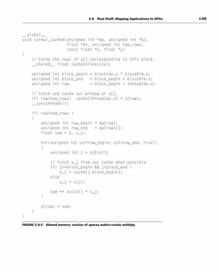
C.8 Real Stuff: Mapping Applications to GPUs C-59
__global__ void csrmul_cached(unsigned int *Ap, unsigned int *Aj, float *Av, unsigned int num_rows, const float *x, float *y){ // Cache the rows of x[] corresponding to this block. __shared__ float cache[blocksize];
unsigned int block_begin = blockIdx.x * blockDim.x; unsigned int block_end = block_begin + blockDim.x; unsigned int row = block_begin + threadIdx.x;
// Fetch and cache our window of x[]. if( row<num_rows) cache[threadIdx.x] = x[row]; __syncthreads();
if( row<num_rows ) { unsigned int row_begin = Ap[row]; unsigned int row_end = Ap[row+1]; float sum = 0, x_j;
for(unsigned int col=row_begin; col<row_end; ++col) { unsigned int j = Aj[col]; // Fetch x_j from our cache when possible if( j>=block_begin && j<block_end ) x_j = cache[j-block_begin]; else x_j = x[j];
sum += Av[col] * x_j; }
y[row] = sum; }}
FIGURE C.8.5 Shared memory version of sparse matrix-vector multiply.
C-60 Appendix C Graphics and Computing GPUs
Th ese are fairly simple kernels whose purpose is to illustrate basic techniques in writing CUDA programs, rather than how to achieve maximal performance. Numerous possible avenues for optimization are available, several of which are explored by Williams, et al. [2007] on a handful of diff erent multicore architectures. Nevertheless, it is still instructive to examine the comparative performance of even these simplistic kernels. On a 2 GHz Intel Core2 Xeon E5335 processor, the csrmul_serial() kernel runs at roughly 202 million nonzeros processed per second, for a collection of Laplacian matrices derived from 3D triangulated surface meshes. Parallelizing this kernel with the parallel_for construct provided by Intel’s Th reading Building Blocks produces parallel speed-ups of 2.0, 2.1, and 2.3 running on two, four, and eight cores of the machine, respectively. On a GeForce 8800 Ultra, the csrmul_kernel() and csrmul_cached() kernels achieve processing rates of roughly 772 and 920 million nonzeros per second, corresponding to parallel speed-ups of 3.8 and 4.6 times over the serial performance of a single CPU core.
Scan and ReductionParallel scan, also known as parallel prefi x sum, is one of the most important building blocks for data-parallel algorithms [Blelloch, 1990]. Given a sequence a of n elements:
[ , , , ]a a an0 1 1… �
and a binary associative operator ⊕, the scan function computes the sequence:
scan( , ) [ ,( ), ,( )]a a a a a a an⊕ ⊕ ⊕ ⊕ ⊕0 0 1 0 1 1… …
As an example, if we take ⊕ to be the usual addition operator, then applying scan to the input array
a � [ ]3 1 7 0 4 1 6 3
will produce the sequence of partial sums:
scan( )a, [ ]3 4 11 11 15 16 22 25
Th is scan operator is an inclusive scan, in the sense that element i of the output sequence incorporates element ai of the input. Incorporating only previous elements would yield an exclusive scan operator, also known as a prefi x-sum operation.
Th e serial implementation of this operation is extremely simple. It is simply a loop that iterates once over the entire sequence, as shown in Figure C.8.6.
At fi rst glance, it might appear that this operation is inherently serial. However, it can actually be implemented in parallel effi ciently. Th e key observation is that

C.8 Real Stuff: Mapping Applications to GPUs C-61
FIGURE C.8.6 Template for serial plus-scan.
FIGURE C.8.7 CUDA template for parallel plus-scan.
template<class T>__host__ T plus_scan(T *x, unsigned int n){ for(unsigned int i=1; i<n; ++i) x[i] = x[i-1] + x[i];}
template<class T>__device__ T plus_scan(T *x){ unsigned int i = threadIdx.x; unsigned int n = blockDim.x;
for(unsigned int offset=1; offset<n; offset *= 2) { T t;
if(i>=offset) t = x[i-offset]; __syncthreads();
if(i>=offset) x[i] = t + x[i]; __syncthreads(); } return x[i];}
because addition is associative, we are free to change the order in which elements are added together. For instance, we can imagine adding pairs of consecutive elements in parallel, and then adding these partial sums, and so on.
One simple scheme for doing this is from Hillis and Steele [1989]. An implementation of their algorithm in CUDA is shown in Figure C.8.7. It assumes that the input array x[ ] contains exactly one element per thread of the thread block. It performs log2 n iterations of a loop collecting partial sums together.
To understand the action of this loop, consider Figure C.8.8, which illustrates the simple case for n � 8 threads and elements. Each level of the diagram represents one step of the loop. Th e lines indicate the location from which the data is being fetched. For each element of the output (i.e., the fi nal row of the diagram) we are building a summation tree over the input elements. Th e edges highlighted in blue show the form of this summation tree for the fi nal element. Th e leaves of this tree are all the initial elements. Tracing back from any output element shows that it incorporates all input values up to and including itself.

C-62 Appendix C Graphics and Computing GPUs
While simple, this algorithm is not as effi cient as we would like. Examining the serial implementation, we see that it performs O(n) additions. Th e parallel implementation, in contrast, performs O(n log n) additions. For this reason, it is not work effi cient, since it does more work than the serial implementation to compute the same result. Fortunately, there are other techniques for implementing scan that are work effi cient. Details on more effi cient implementation techniques and the extension of this per-block procedure to multiblock arrays are provided by Sengupta, et al. [2007].
In some instances, we may only be interested in computing the sum of all elements in an array, rather than the sequence of all prefi x sums returned by scan. Th is is the parallel reduction problem. We could simply use a scan algorithm to perform this computation, but reduction can generally be implemented more effi ciently than scan.
Figure C.8.9 shows the code for computing a reduction using addition. In this example, each thread simply loads one element of the input sequence (i.e., it initially sums a subsequence of length 1). At the end of the reduction, we want thread 0 to hold the sum of all elements initially loaded by the threads of its block. Th e loop in this kernel implicitly builds a summation tree over the input elements, much like the scan algorithm above.
At the end of this loop, thread 0 holds the sum of all the values loaded by this block. If we want the fi nal value of the location pointed to by total to contain the total of all elements in the array, we must combine the partial sums of all the blocks in the grid. One strategy to do this would be to have each block write its partial sum into a second array and then launch the reduction kernel again, repeating the process until we had reduced the sequence to a single value. A more attractive alternative supported by the Tesla GPU architecture is to use the atomicAdd() primitive, an effi cient atomic
FIGURE C.8.8 Tree-based parallel scan data references.
x[0]
x[0]
x[0]
x[0]
x[1]
x[1]
x[1]
x[1]
x[2]
x[2]
x[2]
x[2]
x[3]
x[3]
x[3]
x[3]
x[4]
x[4]
x[4]
x[4]
x[5]
x[5]
x[5]
x[6]
x[6]
x[6]
x[5] x[6] x[7]
x[7] x [ i ] + = x [ i – 1 ] ;
x [ i ] + = x [ i – 2 ] ;
x [ i ] + = x [ i – 4 ] ;
x[7]
x[7]

C.8 Real Stuff: Mapping Applications to GPUs C-63
read-modify-write primitive supported by the memory subsystem. Th is eliminates the need for additional temporary arrays and repeated kernel launches.
Parallel reduction is an essential primitive for parallel programming and highlights the importance of per-block shared memory and low-cost barriers in making cooperation among threads effi cient. Th is degree of data shuffl ing among threads would be prohibitively expensive if done in off -chip global memory.
Radix SortOne important application of scan primitives is in the implementation of sorting routines. Th e code in Figure C.8.10 implements a radix sort of integers across a single thread block. It accepts as input an array values containing one 32-bit integer for each thread of the block. For effi ciency, this array should be stored in per-block shared memory, but this is not required for the sort to behave correctly.
Th is is a fairly simple implementation of radix sort. It assumes the availability of a procedure partition_by_bit() that will partition the given array such that
__global__void plus_reduce(int *input, unsigned int N, int *total){ unsigned int tid = threadIdx.x; unsigned int i = blockIdx.x*blockDim.x + threadIdx.x;
// Each block loads its elements into shared memory, padding // with 0 if N is not a multiple of blocksize __shared__ int x[blocksize]; x[tid] = (i<N) ? input[i] : 0; __syncthreads();
// Every thread now holds 1 input value in x[] // // Build summation tree over elements. for(int s=blockDim.x/2; s>0; s=s/2) { if(tid < s) x[tid] += x[tid + s]; __syncthreads(); }
// Thread 0 now holds the sum of all input values // to this block. Have it add that sum to the running total if( tid == 0 ) atomicAdd(total, x[tid]);}
FIGURE C.8.9 CUDA implementation of plus-reduction.

C-64 Appendix C Graphics and Computing GPUs
all values with a 0 in the designated bit will come before all values with a 1 in that bit. To produce the correct output, this partitioning must be stable.
Implementing the partitioning procedure is a simple application of scan. Th read i holds the value xi and must calculate the correct output index at which to write this value. To do so, it needs to calculate (1) the number of threads j � i for which the designated bit is 1 and (2) the total number of bits for which the designated bit is 0. Th e CUDA code for partition_by_bit() is shown in Figure C.8.11.
__device__ void radix_sort(unsigned int *values){ for(int bit=0; bit<32; ++bit) { partition_by_bit(values, bit); __syncthreads(); }}
FIGURE C.8.10 CUDA code for radix sort.
__device__ void partition_by_bit(unsigned int *values, unsigned int bit){ unsigned int i = threadIdx.x; unsigned int size = blockDim.x; unsigned int x_i = values[i]; unsigned int p_i = (x_i >> bit) & 1;
values[i] = p_i; __syncthreads();
// Compute number of T bits up to and including p_i. // Record the total number of F bits as well. unsigned int T_before = plus_scan(values); unsigned int T_total = values[size-1]; unsigned int F_total = size - T_total; __syncthreads();
// Write every x_i to its proper place if( p_i ) values[T_before-1 + F_total] = x_i; else values[i - T_before] = x_i;}
FIGURE C.8.11 CUDA code to partition data on a bit-by-bit basis, as part of radix sort.
C.8 Real Stuff: Mapping Applications to GPUs C-65
A similar strategy can be applied for implementing a radix sort kernel that sorts an array of large length, rather than just a one-block array. Th e fundamental step remains the scan procedure, although when the computation is partitioned across multiple kernels, we must double-buff er the array of values rather than doing the partitioning in place. Details on performing radix sorts on large arrays effi ciently are provided by Satish et al. [2008].
N-Body Applications on a GPU1
Nyland, et al. [2007] describe a simple yet useful computational kernel with excellent GPU performance—the all-pairs N-body algorithm. It is a time-consuming component of many scientifi c applications. N-body simulations calculate the evolution of a system of bodies in which each body continuously interacts with every other body. One example is an astrophysical simulation in which each body represents an individual star, and the bodies gravitationally attract each other. Other examples are protein folding, where N-body simulation is used to calculate electrostatic and van der Waals forces; turbulent fl uid fl ow simulation; and global illumination in computer graphics.
Th e all-pairs N-body algorithm calculates the total force on each body in the system by computing each pair-wise force in the system, summing for each body. Many scientists consider this method to be the most accurate, with the only loss of precision coming from the fl oating-point hardware operations. Th e drawback is its O(n2) computational complexity, which is far too large for systems with more than 10 bodies. To overcome this high cost, several simplifi cations have been proposed to yield O(n log n) and O(n) algorithms; examples are the Barnes-Hut algorithm, the Fast Multipole Method and Particle-Mesh-Ewald summation. All of the fast methods still rely on the all-pairs method as a kernel for accurate computation of short-range forces; thus it continues to be important.
N-Body Mathematics
For gravitational simulation, calculate the body-body force using elementary physics. Between two bodies indexed by i and j, the 3D force vector is:
fr riji j
ij
ij
ijG
m m�
|| || || ||2 ×r
Th e force magnitude is calculated in the left term, while the direction is computed in the right (unit vector pointing from one body to the other).
Given a list of interacting bodies (an entire system or a subset), the calculation is simple: for all pairs of interactions, compute the force and sum for each body. Once the total forces are calculated, they are used to update each body’s position and velocity, based on the previous position and velocity. Th e calculation of the forces has complexity O(n2), while the update is O(n).
1 Adapted from Nyland et al. [2007], “Fast N-Body Simulation with CUDA,” Chapter 31 of GPU Gems 3.

C-66 Appendix C Graphics and Computing GPUs
Th e serial force-calculation code uses two nested for-loops iterating over pairs of bodies. Th e outer loop selects the body for which the total force is being calculated, and the inner loop iterates over all the bodies. Th e inner loop calls a function that computes the pair-wise force, then adds the force into a running sum.
To compute the forces in parallel, we assign one thread to each body, since the calculation of force on each body is independent of the calculation on all other bodies. Once all of the forces are computed, the positions and velocities of the bodies can be updated.
Th e code for the serial and parallel versions is shown in Figure C.8.12 and Figure C.8.13. Th e serial version has two nested for-loops. Th e conversion to CUDA, like many other examples, converts the serial outer loop to a per-thread kernel where each thread computes the total force on a single body. Th e CUDA kernel computes a global thread ID for each thread, replacing the iterator variable of the serial outer loop. Both kernels fi nish by storing the total acceleration in a global array used to compute the new position and velocity values in a subsequent step.
__global__ void accel_on_one_body(){ int i = threadIdx.x + blockDim.x * blockIdx.x; int j; float3 acc(0.0f, 0.0f, 0.0f);
for (j = 0; j < N; j++) { acc = body_body_interaction(acc, body[i], body[j]); } accel[i] = acc;}
FIGURE C.8.13 CUDA thread code to compute the total force on a single body.
FIGURE C.8.12 Serial code to compute all pair-wise forces on N bodies.
void accel_on_all_bodies(){ int i, j; float3 acc(0.0f, 0.0f, 0.0f);
for (i = 0; i < N; i++) { for (j = 0; j < N; j++) { acc = body_body_interaction(acc, body[i], body[j]); } accel[i] = acc; }}
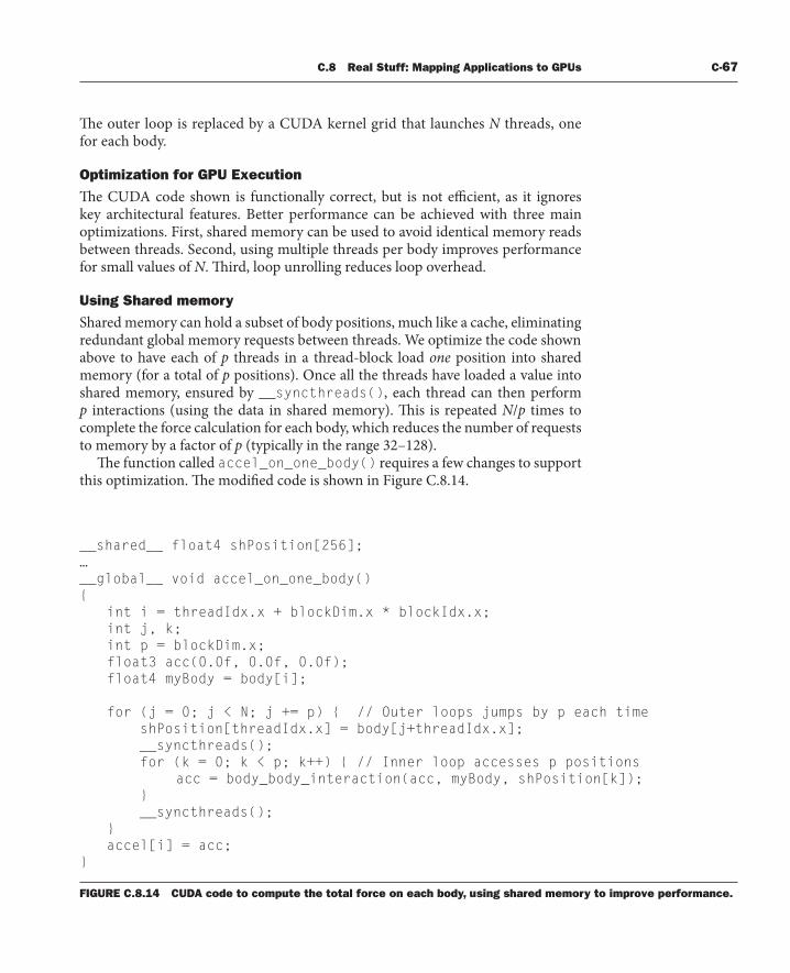
C.8 Real Stuff: Mapping Applications to GPUs C-67
Th e outer loop is replaced by a CUDA kernel grid that launches N threads, one for each body.
Optimization for GPU Execution
Th e CUDA code shown is functionally correct, but is not effi cient, as it ignores key architectural features. Better performance can be achieved with three main optimizations. First, shared memory can be used to avoid identical memory reads between threads. Second, using multiple threads per body improves performance for small values of N. Th ird, loop unrolling reduces loop overhead.
Using Shared memory
Shared memory can hold a subset of body positions, much like a cache, eliminating redundant global memory requests between threads. We optimize the code shown above to have each of p threads in a thread-block load one position into shared memory (for a total of p positions). Once all the threads have loaded a value into shared memory, ensured by __syncthreads(), each thread can then perform p interactions (using the data in shared memory). Th is is repeated N/p times to complete the force calculation for each body, which reduces the number of requests to memory by a factor of p (typically in the range 32–128).
Th e function called accel_on_one_body() requires a few changes to support this optimization. Th e modifi ed code is shown in Figure C.8.14.
__shared__ float4 shPosition[256];…__global__ void accel_on_one_body(){ int i = threadIdx.x + blockDim.x * blockIdx.x; int j, k; int p = blockDim.x; float3 acc(0.0f, 0.0f, 0.0f); float4 myBody = body[i];
for (j = 0; j < N; j += p) { // Outer loops jumps by p each time shPosition[threadIdx.x] = body[j+threadIdx.x]; __syncthreads(); for (k = 0; k < p; k++) { // Inner loop accesses p positions acc = body_body_interaction(acc, myBody, shPosition[k]); } __syncthreads(); } accel[i] = acc;}
FIGURE C.8.14 CUDA code to compute the total force on each body, using shared memory to improve performance.

C-68 Appendix C Graphics and Computing GPUs
Th e loop that formerly iterated over all bodies now jumps by the block dimension p. Each iteration of the outer loop loads p successive positions into shared memory (one position per thread). Th e threads synchronize, and then p force calculations are computed by each thread. A second synchronization is required to ensure that new values are not loaded into shared memory prior to all threads completing the force calculations with the current data.
Using shared memory reduces the memory bandwidth required to less than 10% of the total bandwidth that the GPU can sustain (using less than 5 GB/s). Th is optimization keeps the application busy performing computation rather than waiting on memory accesses, as it would have done without the use of shared memory. Th e performance for varying values of N is shown in Figure C.8.15.
Using Multiple Threads per BodyFigure C.8.15 shows performance degradation for problems with small values of N (N � 4096) on the GeForce 8800 GTX. Many research eff orts that rely on N-body calculations focus on small N (for long simulation times), making it a target of our optimization eff orts. Our presumption to explain the lower performance was that there was simply not enough work to keep the GPU busy when N is small. Th e solution is to allocate more threads per body. We change the thread-block dimensions from (p, 1, 1) to (p, q, 1), where q threads divide the work of a single body into equal parts. By allocating the additional threads within the same thread block, partial results can be stored in shared memory. When all the force calculations are
FIGURE C.8.15 Performance measurements of the N-body application on a GeForce 8800 GTX and a GeForce 9600. Th e 8800 has 128 stream processors at 1.35 GHz, while the 9600 has 64 at 0.80 GHz (about 30% of the 8800). Th e peak performance is 242 GFLOPS. For a GPU with more processors, the problem needs to be bigger to achieve full performance (the 9600 peak is around 2048 bodies, while the 8800 doesn’t reach its peak until 16,384 bodies). For small N, more than one thread per body can signifi cantly improve performance, but eventually incurs a performance penalty as N grows.
250N-Body Performance on GPUs
200
150
100
50
GF
LOP
S
Number of Bodies
0
512
768
1024
1536
2048
3072
4096
6144
8192
12,2
88
16,3
84
24,5
76
32,7
68
1 thread, 8800
2 threads, 8800
4 threads, 8800
1 thread, 9600
2 threads, 9600
4 threads, 9600

C.8 Real Stuff: Mapping Applications to GPUs C-69
done, the q partial results can be collected and summed to compute the fi nal result. Using two or four threads per body leads to large improvements for small N.
As an example, the performance on the 8800 GTX jumps by 110% when N � 1024 (one thread achieves 90 GFLOPS, where four achieve 190 GFLOPS). Performance degrades slightly on large N, so we only use this optimization for N smaller than 4096. Th e performance increases are shown in Figure C.8.15 for a GPU with 128 processors and a smaller GPU with 64 processors clocked at two-thirds the speed.
Performance Comparison
Th e performance of the N-body code is shown in Figure C.8.15 and Figure C.8.16. In Figure C.8.15, performance of high- and medium-performance GPUs is shown, along with the performance improvements achieved by using multiple threads per body. Th e performance on the faster GPU ranges from 90 to just under 250 GFLOPS.
Figure C.8.16 shows nearly identical code (C�� versus CUDA) running on Intel Core2 CPUs. Th e CPU performance is about 1% of the GPU, in the range of 0.2 to 2 GFLOPS, remaining nearly constant over the wide range of problem sizes.
FIGURE C.8.16 Performance measurements on the N-body code on a CPU. Th e graph shows single precision N-body performance using Intel Core2 CPUs, denoted by their CPU model number. Note the dramatic reduction in GFLOPS performance (shown in GFLOPS on the y-axis), demonstrating how much faster the GPU is compared to the CPU. Th e performance on the CPU is generally independent of problem size, except for an anomalously low performance when N�16,384 on the X9775 CPU. Th e graph also shows the results of running the CUDA version of the code (using the CUDA-for-CPU compiler) on a single CPU core, where it outperforms the C�� code by 24%. As a programming language, CUDA exposes parallelism and locality that a compiler can exploit. Th e Intel CPUs are a 3.2 GHz Extreme X9775 (code named “Penryn”), a 2.66 GHz E8200 (code named “Wolfdale”), a desktop, pre-Penryn CPU, and a 1.83 GHz T2400 (code named “Yonah”), a 2007 laptop CPU. Th e Penryn version of the Core 2 architecture is particularly interesting for N-body calculations with its 4-bit divider, allowing division and square root operations to execute four times faster than previous Intel CPUs.
Number of Bodies
N-Body Performance on Intel CPUs2
1.8
1.6
1.4
1.2
1
0.8
0.6
0.4
0.2
0
512
GF
LOP
S
768
1024
1536
2048
3072
4096
6144
8192
12,2
88
16,3
84
24,5
76
32,7
68
T2400
E8200
X9775
X9775-Cuda
C-70 Appendix C Graphics and Computing GPUs
Th e graph also shows the results of compiling the CUDA version of the code for a CPU, where the performance improves by 24%. CUDA, as a programming language, exposes parallelism, allowing the compiler to make better use of the SSE vector unit on a single core. Th e CUDA version of the N-body code naturally maps to multicore CPUs as well (with grids of blocks), where it achieves nearly perfect scaling on an eight-core system with N � 4096 (ratios of 2.0, 3.97, and 7.94 on two, four, and eight cores, respectively).
Results
With a modest eff ort, we developed a computational kernel that improves GPU performance over multicore CPUs by a factor of up to 157. Execution time for the N-body code running on a recent CPU from Intel (Penryn X9775 at 3.2 GHz, single core) took more than 3 seconds per frame to run the same code that runs at a 44 Hz frame rate on a GeForce 8800 GPU. On pre-Penryn CPUs, the code requires 6–16 seconds, and on older Core2 processors and Pentium IV processor, the time is about 25 seconds. We must divide the apparent increase in performance in half, as the CPU requires only half as many calculations to compute the same result (using the optimization that the forces on a pair of bodies are equal in strength and opposite in direction).
How can the GPU speed up the code by such a large amount? Th e answer requires inspecting architectural details. Th e pair-wise force calculation requires 20 fl oating-point operations, comprised mostly of addition and multiplication instructions (some of which can be combined using a multiply-add instruction), but there are also division and square root instructions for vector normalization. Intel CPUs take many cycles for single precision division and square root instructions,2 although this has improved in the latest Penryn CPU family with its faster 4-bit divider.3 Additionally, the limitations in register capacity lead to many MOV instructions in the x86 code (presumably to/from L1 cache). In contrast, the GeForce 8800 executes a reciprocal square-root thread instruction in four clocks; see Section C.6 for special function accuracy. It has a larger register fi le (per thread) and shared memory that can be accessed as an instruction operand. Finally, the CUDA compiler emits 15 instructions for one iteration of the loop, compared with more than 40 instructions from a variety of x86 CPU compilers. Greater parallelism, faster execution of complex instructions, more register space, and an effi cient compiler all combine to explain the dramatic performance improvement of the N-body code between the CPU and the GPU.
2 Th e x86 SSE instructions reciprocal-square-root (RSQRT*) and reciprocal (RCP*) were not considered, as their accuracy is too low to be comparable.3 Intel Corporation, Intel 64 and IA-32 Architectures Optimization Reference Manual. November 2007. Order Number: 248966-016. Also available at www3.intel.com/design/processor/manuals/248966.pdf.

C.8 Real Stuff: Mapping Applications to GPUs C-71
On a GeForce 8800, the all-pairs N-body algorithm delivers more than 240 GFLOPS of performance, compared to less than 2 GFLOPS on recent sequential processors. Compiling and executing the CUDA version of the code on a CPU demonstrates that the problem scales well to multicore CPUs, but is still signifi cantly slower than a single GPU.
We coupled the GPU N-body simulation with a graphical display of the motion, and can interactively display 16K bodies interacting at 44 frames per second. Th is allows astrophysical and biophysical events to be displayed and navigated at interactive rates. Additionally, we can parameterize many settings, such as noise reduction, damping, and integration techniques, immediately displaying their eff ects on the dynamics of the system. Th is provides scientists with stunning visual imagery, boosting their insights on otherwise invisible systems (too large or small, too fast or too slow), allowing them to create better models of physical phenomena.
Figure C.8.17 shows a time-series display of an astrophysical simulation of 16K bodies, with each body acting as a galaxy. Th e initial confi guration is a
FIGURE C.8.17 12 images captured during the evolution of an N-body system with 16,384 bodies.

C-72 Appendix C Graphics and Computing GPUs
spherical shell of bodies rotating about the z-axis. One phenomenon of interest to astrophysicists is the clustering that occurs, along with the merging of galaxies over time. For the interested reader, the CUDA code for this application is available in the CUDA SDK from www.nvidia.com/CUDA.
C.9 Fallacies and Pitfalls
GPUs have evolved and changed so rapidly that many fallacies and pitfalls have arisen. We cover a few here.
Fallacy: GPUs are just SIMD vector multiprocessors. It is easy to draw the false conclusion that GPUs are simply SIMD vector multiprocessors. GPUs do have a SPMD-style programming model, in that a programmer can write a single program that is executed in multiple thread instances with multiple data. Th e execution of these threads is not purely SIMD or vector, however; it is single-instruction multiple-thread (SIMT), described in Section C.4. Each GPU thread has its own scalar registers, thread private memory, thread execution state, thread ID, independent execution and branch path, and eff ective program counter, and can address memory independently. Although a group of threads (e.g., a warp of 32 threads) executes more effi ciently when the PCs for the threads are the same, this is not necessary. So, the multiprocessors are not purely SIMD. Th e thread execution model is MIMD with barrier synchronization and SIMT optimizations. Execution is more effi cient if individual thread load/store memory accesses can be coalesced into block accesses, as well. However, this is not strictly necessary. In a purely SIMD vector architecture, memory/register accesses for diff erent threads must be aligned in a regular vector pattern. A GPU has no such restriction for register or memory accesses; however, execution is more effi cient if warps of threads access local blocks of data.
In a further departure from a pure SIMD model, an SIMT GPU can execute more than one warp of threads concurrently. In graphics applications, there may be multiple groups of vertex programs, pixel programs, and geometry programs running in the multiprocessor array concurrently. Computing programs may also execute diff erent programs concurrently in diff erent warps.
Fallacy: GPU performance cannot grow faster than Moore’s law. Moore’s law is simply a rate. It is not a “speed of light” limit for any other rate. Moore’s law describes an expectation that, over time, as semiconductor technology advances and transistors become smaller, the manufacturing cost per transistor will decline

C.9 Fallacies and Pitfalls C-73
exponentially. Put another way, given a constant manufacturing cost, the number of transistors will increase exponentially. Gordon Moore [1965] predicted that this progression would provide roughly two times the number of transistors for the same manufacturing cost every year, and later revised it to doubling every two years. Although Moore made the initial prediction in 1965 when there were just 50 components per integrated circuit, it has proved remarkably consistent. Th e reduction of transistor size has historically had other benefi ts, such as lower power per transistor and faster clock speeds at constant power.
Th is increasing bounty of transistors is used by chip architects to build processors, memory, and other components. For some time, CPU designers have used the extra transistors to increase processor performance at a rate similar to Moore’s law, so much so that many people think that processor performance growth of two times every 18–24 months is Moore’s law. In fact, it is not.
Microprocessor designers spend some of the new transistors on processor cores, improving the architecture and design, and pipelining for more clock speed. Th e rest of the new transistors are used for providing more cache, to make memory access faster. In contrast, GPU designers use almost none of the new transistors to provide more cache; most of the transistors are used for improving the processor cores and adding more processor cores.
GPUs get faster by four mechanisms. First, GPU designers reap the Moore’s law bounty directly by applying exponentially more transistors to building more parallel, and thus faster, processors. Second, GPU designers can improve on the architecture over time, increasing the effi ciency of the processing. Th ird, Moore’s law assumes constant cost, so the Moore’s law rate can clearly be exceeded by spending more for larger chips with more transistors. Fourth, GPU memory systems have increased their eff ective bandwidth at a pace nearly comparable to the processing rate, by using faster memories, wider memories, data compression, and better caches. Th e combination of these four approaches has historically allowed GPU performance to double regularly, roughly every 12 to 18 months. Th is rate, exceeding the rate of Moore’s law, has been demonstrated on graphics applications for approximately ten years and shows no sign of signifi cant slowdown. Th e most challenging rate limiter appears to be the memory system, but competitive innovation is advancing that rapidly too.
Fallacy: GPUs only render 3D graphics; they can’t do general computation. GPUs are built to render 3D graphics as well as 2D graphics and video. To meet the demands of graphics soft ware developers as expressed in the interfaces and performance/feature requirements of the graphics APIs, GPUs have become massively parallel programmable fl oating-point processors. In the graphics domain, these processors are programmed through the graphics APIs and with arcane graphics programming languages (GLSL, Cg, and HLSL, in OpenGL and Direct3D). However, there is

C-74 Appendix C Graphics and Computing GPUs
nothing preventing GPU architects from exposing the parallel processor cores to programmers without the graphics API or the arcane graphics languages.
In fact, the Tesla architecture family of GPUs exposes the processors through a soft ware environment known as CUDA, which allows programmers to develop general application programs using the C language and soon C��. GPUs are Turing-complete processors, so they can run any program that a CPU can run, although perhaps less well. And perhaps faster.
Fallacy: GPUs cannot run double precision fl oating-point programs fast. In the past, GPUs could not run double precision fl oating-point programs at all, except through soft ware emulation. And that’s not very fast at all. GPUs have made the progression from indexed arithmetic representation (lookup tables for colors) to 8-bit integers per color component, to fi xed-point arithmetic, to single precision fl oating-point, and recently added double precision. Modern GPUs perform virtually all calculations in single precision IEEE fl oating-point arithmetic, and are beginning to use double precision in addition.
For a small additional cost, a GPU can support double precision fl oating-point as well as single precision fl oating-point. Today, double precision runs more slowly than the single precision speed, about fi ve to ten times slower. For incremental additional cost, double precision performance can be increased relative to single precision in stages, as more applications demand it.
Fallacy: GPUs don’t do fl oating-point correctly. GPUs, at least in the Tesla architecture family of processors, perform single precision fl oating-point processing at a level prescribed by the IEEE 754 fl oating-point standard. So, in terms of accuracy, GPUs are the equal of any other IEEE 754-compliant processors.
Today, GPUs do not implement some of the specifi c features described in the standard, such as handling denormalized numbers and providing precise fl oating-point exceptions. However, the recently introduced Tesla T10P GPU provides full IEEE rounding, fused-multiply-add, and denormalized number support for double precision.
Pitfall: Just use more threads to cover longer memory latencies. CPU cores are typically designed to run a single thread at full speed. To run at full speed, every instruction and its data need to be available when it is time for that instruction to run. If the next instruction is not ready or the data required for that instruction is not available, the instruction cannot run and the processor stalls. External memory is distant from the processor, so it takes many cycles of wasted execution to fetch data from memory. Consequently, CPUs require large local caches to keep running

C.9 Fallacies and Pitfalls C-75
without stalling. Memory latency is long, so it is avoided by striving to run in the cache. At some point, program working set demands may be larger than any cache. Some CPUs have used multithreading to tolerate latency, but the number of threads per core has generally been limited to a small number.
Th e GPU strategy is diff erent. GPU cores are designed to run many threads concurrently, but only one instruction from any thread at a time. Another way to say this is that a GPU runs each thread slowly, but in aggregate runs the threads effi ciently. Each thread can tolerate some amount of memory latency, because other threads can run.
Th e downside of this is that multiple—many multiple threads—are required to cover the memory latency. In addition, if memory accesses are scattered or not correlated among threads, the memory system will get progressively slower in responding to each individual request. Eventually, even the multiple threads will not be able to cover the latency. So, the pitfall is that for the “just use more threads” strategy to work for covering latency, you have to have enough threads, and the threads have to be well-behaved in terms of locality of memory access.
Fallacy: O(n) algorithms are diffi cult to speed up. No matter how fast the GPU is at processing data, the steps of transferring data to and from the device may limit the performance of algorithms with O(n) complexity (with a small amount of work per datum). Th e highest transfer rate over the PCIe bus is approximately 48 GB/second when DMA transfers are used, and slightly less for nonDMA transfers. Th e CPU, in contrast, has typical access speeds of 8–12 GB/second to system memory. Example problems, such as vector addition, will be limited by the transfer of the inputs to the GPU and the returning output from the computation.
Th ere are three ways to overcome the cost of transferring data. First, try to leave the data on the GPU for as long as possible, instead of moving the data back and forth for diff erent steps of a complicated algorithm. CUDA deliberately leaves data alone in the GPU between launches to support this.
Second, the GPU supports the concurrent operations of copy-in, copy-out and computation, so data can be streamed in and out of the device while it is computing. Th is model is useful for any data stream that can be processed as it arrives. Examples are video processing, network routing, data compression/decompression, and even simpler computations such as large vector mathematics.
Th e third suggestion is to use the CPU and GPU together, improving performance by assigning a subset of the work to each, treating the system as a heterogeneous computing platform. Th e CUDA programming model supports allocation of work to one or more GPUs along with continued use of the CPU without the use of threads (via asynchronous GPU functions), so it is relatively simple to keep all GPUs and a CPU working concurrently to solve problems even faster.

C-76 Appendix C Graphics and Computing GPUs
C.10 Concluding Remarks
GPUs are massively parallel processors and have become widely used, not only for 3D graphics, but also for many other applications. Th is wide application was made possible by the evolution of graphics devices into programmable processors. Th e graphics application programming model for GPUs is usually an API such as DirectX™ or OpenGL™. For more general-purpose computing, the CUDA programming model uses an SPMD (single-program multiple data) style, executing a program with many parallel threads.
GPU parallelism will continue to scale with Moore’s law, mainly by increasing the number of processors. Only the parallel programming models that can readily scale to hundreds of processor cores and thousands of threads will be successful in supporting manycore GPUs and CPUs. Also, only those applications that have many largely independent parallel tasks will be accelerated by massively parallel manycore architectures.
Parallel programming models for GPUs are becoming more fl exible, for both graphics and parallel computing. For example, CUDA is evolving rapidly in the direction of full C/C�� functionality. Graphics APIs and programming models will likely adapt parallel computing capabilities and models from CUDA. Its SPMD-style threading model is scalable, and is a convenient, succinct, and easily learned model for expressing large amounts of parallelism.
Driven by these changes in the programming models, GPU architecture is in turn becoming more fl exible and more programmable. GPU fi xed-function units are becoming accessible from general programs, along the lines of how CUDA programs already use texture intrinsic functions to perform texture lookups using the GPU texture instruction and texture unit.
GPU architecture will continue to adapt to the usage patterns of both graphics and other application programmers. GPUs will continue to expand to include more processing power through additional processor cores, as well as increasing the thread and memory bandwidth available for programs. In addition, the programming models must evolve to include programming heterogeneous manycore systems including both GPUs and CPUs.
AcknowledgmentsTh is appendix is the work of several authors at NVIDIA. We gratefully acknowledge the signifi cant contributions of Michael Garland, John Montrym, Doug Voorhies, Lars Nyland, Erik Lindholm, Paulius Micikevicius, Massimiliano Fatica, Stuart Oberman, and Vasily Volkov.

C.11 Historical Perspective and Further Reading C-77
C.11 Historical Perspective and Further Reading
Graphics Pipeline Evolution3D graphics pipeline hardware evolved from the large expensive systems of the early 1980s to small workstations and then to PC accelerators in the mid- to late 1990s. During this period, three major transitions occurred:
■ Performance-leading graphics subsystems declined in price from $50,000 to $200.
■ Performance increased from 50 million pixels per second to 1 billion pixels per second and from 100,000 vertices per second to 10 million vertices per second.
■ Native hardware capabilities evolved from wireframe (polygon outlines) to fl at shaded (constant color) fi lled polygons, to smooth shaded (interpolated color) fi lled polygons, to full-scene anti-aliasing with texture mapping and rudimentary multitexturing.
Fixed-Function Graphics PipelinesTh roughout this period, graphics hardware was confi gurable, but not programmable by the application developer. With each generation, incremental improvements were off ered. But developers were growing more sophisticated and asking for more new features than could be reasonably off ered as built-in fi xed functions. Th e NVIDIA GeForce 3, described by Lindholm et al. [2001], took the fi rst step toward true general shader programmability. It exposed to the application developer what had been the private internal instruction set of the fl oating-point vertex engine. Th is coincided with the release of Microsoft ’s DirectX 8 and OpenGL’s vertex shader extensions. Later GPUs, at the time of DirectX 9, extended general programmability and fl oating point capability to the pixel fragment stage, and made texture available at the vertex stage. Th e ATI Radeon 9700, introduced in 2002, featured a programmable 24-bit fl oating-point pixel fragment processor programmed with DirectX 9 and OpenGL. Th e GeForce FX added 32-bit fl oating-point pixel processors. Th is was part of a general trend toward unifying the functionality of the diff erent stages, at least as far as the application programmer was concerned. NVIDIA’s GeForce 6800 and 7800 series were built with separate processor designs and separate hardware dedicated to the vertex and to the fragment processing. Th e XBox 360 introduced an early unifi ed processor GPU in 2005, allowing vertex and pixel shaders to execute on the same processor.
C-78 Appendix C Graphics and Computing GPUs
Evolution of Programmable Real-Time GraphicsDuring the last 30 years, graphics architecture has evolved from a simple pipeline for drawing wireframe diagrams to a highly parallel design consisting of several deep parallel pipelines capable of rendering complex interactive imagery that appears three-dimensional. Concurrently, many of the calculations involved became far more sophisticated and user programmable.
In these graphics pipelines, certain stages do a great deal of fl oating-point arithmetic on completely independent data, such as transforming the position of triangle vertexes or generating pixel colors. Th is data independence is a key diff erence between GPUs and CPUs. A single frame, rendered in 1/60th of a second, might have 1 million triangles and 6 million pixels. Th e opportunity to use hardware parallelism to exploit this data independence is tremendous.
Th e specifi c functions executed at a few graphics pipeline stages vary with rendering algorithms and have evolved to be programmable. Vertex programs map the position of triangle vertices on to the screen, altering their position, color, or orientation. Typically a vertex shader thread inputs a fl oating-point (x, y, z, w) vertex position and computes a fl oating-point (x, y, z) screen position. Geometry programs operate on primitives defi ned by multiple vertices, changing them or generating additional primitives. Pixel fragment shaders each “shade” one pixel, computing a fl oating-point red, green, blue, alpha (RGBA) color contribution to the rendered image at its pixel sample (x, y) image position. For all three types of graphics shaders, program instances can be run in parallel, because each works on independent data, produces independent results, and has no side eff ects.
Between these programmable graphics pipeline stages are dozens of fi xed-function stages which perform well-defi ned tasks far more effi ciently than a programmable processor could and which would benefi t far less from programmability. For example, between the geometry processing stage and the pixel processing stage is a “rasterizer,” a complex state machine that determines exactly which pixels (and portions thereof) lie within each geometric primitive’s boundaries. Together, the mix of programmable and fi xed-function stages is engineered to balance extreme performance with user control over the rendering algorithms.
Common rendering algorithms perform a single pass over input primitives and access other memory resources in a highly coherent manner; these algorithms provide excellent bandwidth utilization and are largely insensitive to memory latency. Combined with a pixel shader workload that is usually compute-limited, these characteristics have guided GPUs along a diff erent evolutionary path than CPUs. Whereas CPU die area is dominated by cache memory, GPUs are dominated by fl oating-point datapath and fi xed-function logic. GPU memory interfaces emphasize bandwidth over latency (since latency can be readily hidden by a high thread count); indeed, bandwidth is typically many times higher than a CPU, exceeding 100 GB/second in some cases. Th e far-higher number of fi ne-grained lightweight threads eff ectively exploits the rich parallelism available.

C.11 Historical Perspective and Further Reading C-79
Beginning with NVIDIA’s GeForce 8800 GPU in 2006, the three programmable graphics stages are mapped to an array of unifi ed processors; the logical graphics pipeline is physically a recirculating path that visits these processors three times, with much fi xed-function graphics logic between visits. Since diff erent rendering algorithms present wildly diff erent loads among the three programmable stages, this unifi cation provides processor load balancing.
Unifi ed Graphics and Computing ProcessorsBy the DirectX 10 generation, the functionality of vertex and pixel fragment shaders was to be made identical to the programmer, and in fact a new logical stage was introduced, the geometry shader, to process all the vertices of a primitive rather than vertices in isolation. Th e GeForce 8800 was designed with DirectX 10 in mind. Developers were coming up with more sophisticated shading algorithms, and this motivated a sharp increase in the available shader operation rate, particularly fl oating-point operations. NVIDIA chose to pursue a processor design with higher operating frequency than standard-cell methodologies had allowed, to deliver the desired operation throughput as area-effi ciently as possible. High-clock-speed design requires substantially more engineering eff ort, and this favored designing one processor, rather than two (or three, given the new geometry stage). It became worthwhile to take on the engineering challenges of a unifi ed processor (load balancing and recirculation of a logical pipeline onto threads of the processor array) to get the benefi ts of one processor design.
GPGPU: an Intermediate StepAs DirectX 9-capable GPUs became available, some researchers took notice of the raw performance growth path of GPUs and began to explore the use of GPUs to solve complex parallel problems. DirectX 9 GPUs had been designed only to match the features required by the graphics API. To access the computational resources, a programmer had to cast their problem into native graphics operations. For example, to run many simultaneous instances of a pixel shader, a triangle had to be issued to the GPU (with clipping to a rectangle shape if that’s what was desired). Shaders did not have the means to perform arbitrary scatter operations to memory. Th e only way to write a result to memory was to emit it as a pixel color value, and confi gure the framebuff er operation stage to write (or blend, if desired) the result to a two-dimensional framebuff er. Furthermore, the only way to get a result from one pass of computation to the next was to write all parallel results to a pixel framebuff er, then use that framebuff er as a texture map as input to the pixel fragment shader of the next stage of the computation. Mapping general computations to a GPU in this era was quite awkward. Nevertheless, intrepid researchers demonstrated a handful of useful applications with painstaking eff orts. Th is fi eld was called “GPGPU” for general purpose computing on GPUs.

C-80 Appendix C Graphics and Computing GPUs
GPU ComputingWhile developing the Tesla architecture for the GeForce 8800, NVIDIA realized its potential usefulness would be much greater if programmers could think of the GPU as a processor. NVIDIA selected a programming approach in which programmers would explicitly declare the data-parallel aspects of their workload.
For the DirectX 10 generation, NVIDIA had already begun work on a high-effi ciency fl oating-point and integer processor that could run a variety of simultaneous workloads to support the logical graphics pipeline. Th is processor was designed to take advantage of the common case of groups of threads executing the same code path. NVIDIA added memory load and store instructions with integer byte addressing to support the requirements of compiled C programs. It introduced the thread block (cooperative thread array), grid of thread blocks, and barrier synchronization to dispatch and manage highly parallel computing work. Atomic memory operations were added. NVIDIA developed the CUDA C/C�� compiler, libraries, and runtime soft ware to enable programmers to readily access the new data-parallel computation model and develop applications.
Scalable GPUsScalability has been an attractive feature of graphics systems from the beginning. Workstation graphics systems gave customers a choice in pixel horsepower by varying the number of pixel processor circuit boards installed. Prior to the mid-1990s PC graphics scaling was almost nonexistent. Th ere was one option—the VGA controller. As 3D-capable accelerators appeared, the market had room for a range of off erings. 3dfx introduced multiboard scaling with the original SLI (Scan Line Interleave) on their Voodoo2, which held the performance crown for its time (1998). Also in 1998, NVIDIA introduced distinct products as variants on a single architecture with Riva TNT Ultra (high-performance) and Vanta (low-cost), fi rst by speed binning and packaging, then with separate chip designs (GeForce 2 GTS & GeForce 2 MX). At present, for a given architecture generation, four or fi ve separate GPU chip designs are needed to cover the range of desktop PC performance and price points. In addition, there are separate segments in notebook and workstation systems. Aft er acquiring 3dfx, NVIDIA continued the multi-GPU SLI concept in 2004, starting with GeForce 6800—providing multi-GPU scalability transparently to the programmer and to the user. Functional behavior is identical across the scaling range; one application will run unchanged on any implementation of an architectural family.
CPUs are scaling to higher transistor counts by increasing the number of constant-performance cores on a die, rather than increasing the performance of a single core. At this writing the industry is transitioning from dual-core to quad-core, with eight-core not far behind. Programmers are forced to fi nd fourfold to eightfold task parallelism to fully utilize these processors, and applications using task parallelism must be rewritten frequently to target each successive doubling of

C.11 Historical Perspective and Further Reading C-81
core count. In contrast, the highly multithreaded GPU encourages the use of many-fold data parallelism and thread parallelism, which readily scales to thousands of parallel threads on many processors. Th e GPU scalable parallel programming model for graphics and parallel computing is designed for transparent and portable scalability. A graphics program or CUDA program is written once and runs on a GPU with any number of processors. As shown in Section C.1, a CUDA programmer explicitly states both fi ne-grained and coarse-grained parallelism in a thread program by decomposing the problem into grids of thread blocks—the same program will run effi ciently on GPUs or CPUs of any size in current and future generations as well.
Recent DevelopmentsAcademic and industrial work on applications using CUDA has produced hundreds of examples of successful CUDA programs. Many of these programs run the application tens or hundreds of times faster than multicore CPUs are capable of running them. Examples include n-body simulation, molecular modeling, computational fi nance, and oil and gas exploration data processing. Although many of these use single precision fl oating-point arithmetic, some problems require double precision. Th e recent arrival of double precision fl oating point in GPUs enables an even broader range of applications to benefi t from GPU acceleration.
For a comprehensive list and examples of current developments in applications that are accelerated by GPUs, visit CUDAZone: www.nvidia.com/CUDA.
Future TrendsNaturally, the number of processor cores will continue to increase in proportion to increases in available transistors as silicon processes improve. In addition, GPUs will continue to enjoy vigorous architectural evolution. Despite their demonstrated high performance on data-parallel applications, GPU core processors are still of relatively simple design. More aggressive techniques will be introduced with each successive architecture to increase the actual utilization of the calculating units. Because scalable parallel computing on GPUs is a new fi eld, novel applications are rapidly being created. By studying them, GPU designers will discover and implement new machine optimizations.
Further ReadingAkeley, K. and T. Jermoluk [1988]. “High-Performance Polygon Rendering,” Proc. SIGGRAPH 1988 (August), 239–46.
Akeley, K. [1993]. “RealityEngine Graphics.” Proc. SIGGRAPH 1993 (August), 109–16.
Blelloch, G. B. [1990]. “Prefi x Sums and Th eir Applications.” In John H. Reif (Ed.), Synthesis of Parallel Algorithms, Morgan Kaufmann Publishers, San Francisco.
Blythe, D. [2006]. “Th e Direct3D 10 System,” ACM Trans. Graphics, Vol. 25, no. 3 (July), 724–34.

C-82 Appendix C Graphics and Computing GPUs
Buck, I., T. Foley, D. Horn, J. Sugerman, K. Fatahlian, M. Houston, and P. Hanrahan [2004]. “Brook for GPUs: Stream Computing on Graphics Hardware.” Proc. SIGGRAPH 2004, 777–86, August. http://doi.acm.org/10.1145/1186562.1015800
Elder, G. [2002] “Radeon 9700.” Eurographics/SIGGRAPH Workshop on Graphics Hardware, Hot3D Session, www.graphicshardware.org/previous/www_2002/presentations/Hot3D-RADEON9700.ppt
Fernando, R. and M. J. Kilgard [2003]. Th e Cg Tutorial: Th e Defi nitive Guide to Programmable Real-Time Graphics, Addison-Wesley, Reading, MA.
Fernando, R. ed. [2004]. GPU Gems: Programming Techniques, Tips, and Tricks for Real-Time Graphics, Addison-Wesley, Reading, MA. http://developer.nvidia.com/object/gpu_gems_home.html.
Foley, J., A. van Dam, S. Feiner, and J. Hughes [1995]. Computer Graphics: Principles and Practice, second edition in C, Addison-Wesley, Reading, MA.
Hillis, W. D. and G. L. Steele [1986]. “Data parallel algorithms.” Commun. ACM 29, 12 (Dec.), 1170–83. http:// doi.acm.org/10.1145/7902.7903.
IEEE Std 754-2008 [2008]. IEEE Standard for Floating-Point Arithmetic. ISBN 978-0-7381-5752-8, STD95802, http://ieeexplore.ieee.org/servlet/opac?punumber�4610933 (Aug. 29).
Industrial Light and Magic [2003]. OpenEXR, www.openexr.com.
Intel Corporation [2007]. Intel 64 and IA-32 Architectures Optimization Reference Manual. November. Order Number: 248966-016. Also: www3.intel.com/design/processor/manuals/248966.pdf.
Kessenich, J. [2006]. Th e OpenGL Shading Language, Language Version 1.20, Sept. 2006. www.opengl.org/documentation/specs/.
Kirk, D. and D. Voorhies [1990]. “Th e Rendering Architecture of the DN10000VS.” Proc. SIGGRAPH 1990 (August), 299–307.
Lindholm E., M. J. Kilgard, and H. Moreton [2001]. “A User- Programmable Vertex Engine.” Proc. SIGGRAPH 2001 (August), 149–58.
Lindholm E., J. Nickolls, S. Oberman, and J. Montrym [2008]. “NVIDIA Tesla: A Unifi ed Graphics and Computing Architecture.” IEEE Micro, Vol. 28, no. 2 (March–April), 39–55.
Microsoft Corporation. Microsoft DirectX Specifi cation, http://msdn.microsoft .com/directx/
Microsoft Corporation. [2003]. Microsoft DirectX 9 Programmable Graphics Pipeline, Microsoft Press, Redmond, WA.
Montrym, J., D. Baum, D. Dignam, and C. Migdal [1997]. “Infi niteReality: A Real-Time Graphics System.” Proc. SIGGRAPH 1997 (August), 293–301 .
Montrym, J. and H. Moreton [2005]. “Th e GeForce 6800,” IEEE Micro, Vol. 25, no. 2 (March–April), 41–51.
Moore, G. E. [1965]. “Cramming more components onto integrated circuits,” Electronics, Vol. 38, no. 8 (April 19).
Nguyen, H., ed. [2008]. GPU Gems 3, Addison-Wesley, Reading, MA.
C.11 Historical Perspective and Further Reading C-83
Nickolls, J., I. Buck, M. Garland, and K. Skadron [2008]. “Scalable Parallel Programming with CUDA,” ACM Queue, Vol. 6, no. 2 (March–April) 40–53.
NVIDIA [2007]. CUDA Zone. www.nvidia.com/CUDA.
NVIDIA [2007]. CUDA Programming Guide 1.1. http://developer.download.nvidia.com/compute/cuda/1_1/NVIDIA_CUDA_Programming_Guide_1.1.pdf.
NVIDIA [2007]. PTX: Parallel Th read Execution ISA version 1.1. www.nvidia.com/object/io_1195170102263. html.
Nyland, L., M. Harris, and J. Prins [2007]. “Fast N-Body Simulation with CUDA.” In GPU Gems 3, H. Nguyen (Ed.), Addison-Wesley, Reading, MA.
Oberman, S. F. and M. Y. Siu [2005]. “A High-Performance Area- Effi cient Multifunction Interpolator,” Proc. Seventeenth IEEE Symp. Computer Arithmetic, 272–79.
Patterson, D. A. and J. L. Hennessy [2004]. Computer Organization and Design: Th e Hardware/Soft ware Inter face, third edition, Morgan Kaufmann Publishers, San Francisco.
Pharr, M. ed. [2005]. GPU Gems 2: Programming Techniques for High-Performance Graphics and General-Purpose Computation, Addison-Wesley, Reading, MA.
Satish, N., M. Harris, and M. Garland [2008]. “Designing Effi cient Sorting Algorithms for Manycore GPUs,” NVIDIA Technical Report NVR-2008-001.
Segal, M. and K. Akeley [2006]. Th e OpenGL Graphics System: A Specifi cation, Version 2.1, Dec. 1, 2006. www.opengl.org/documentation/specs/.
Sengupta, S., M. Harris, Y. Zhang, and J. D. Owens [2007]. “Scan Primitives for GPU Computing.” In Proc. of Graphics Hardware 2007 (August), 97–106.
Volkov, V. and J. Demmel [2008]. “LU, QR and Cholesky Factorizations using Vector Capabilities of GPUs,” Technical Report No. UCB/EECS-2008-49, 1–11. www.eecs.berkeley.edu/Pubs/TechRpts/2008/EECS-2008-49.html.
Williams, S., L. Oliker, R. Vuduc, J. Shalf, K. Yelick, and J. Demmel [2007]. “Optimization of sparse matrix-vector multiplication on emerging multicore platforms,” In Proc. Supercomputing 2007, November.