Embed Size (px)
Citation preview
Crystalfontz America, Incorporated
GRAPHIC OLED MODULE SPECIFICATIONS
Crystalfontz America, Incorporated12412 East Saltese Avenue
Spokane Valley, WA 99216-0357
Phone: 888-206-9720Fax: 509-892-1203Email: [email protected]: www.crystalfontz.com
Crystalfontz Model Number CFAL12822A-Y-B
Hardware Version Revision 07.07.16, September 2008
Data Sheet Version Revision 1.1, August 2009
Product Pages www.crystalfontz.com/product/CFAL12822A-Y-B.html
Crystalfontz America, Inc. CFAL12822A-Y-B Graphic OLED Module Data Sheetwww.crystalfontz.com Hardware v07.07.16 / Data Sheet v1.1August 2009 Page 2
REVISION HISTORY
HARDWARE
2008/09/02Current hardware version: vANew module.
DATA SHEET
2009/08/11
Current Data Sheet version: v1.1Since last revision (v1.0): In MAIN FEATURES (Pg. 6), announced availability of
DMO-L12822AYB, a new demonstration and evaluation board kit that includes this module.
Removed references to “full color” in Comparison to LCD (Liquid Crystal Display) Module (Pg. 6). Not applicable.
Changed height dimension from “29.95” to “31.00” millimeters under Features (Pg. 6). This includes the bent portion of the FPC (Flexible Printed Circuit) tail that extends beyond the PCB. The “31.00” mm height was already listed in Physical Characteristics (Pg. 7) and Module Outline Drawing (Pg. 8).
Improved wording to describe overall dimensions in Module Outline Drawing (Pg. 8). Dimensions did not change.
Improved System Block Diagram (Pg. 9) by making controller pins links to APPENDIX D: SOLOMON SYSTECH SSD1305 CONTROLLER SPECIFICATION SHEET (Pg. 29).
In DC Characteristics (3.0v Operation) (Pg. 10), changed Logic Supply Voltage for typical from “+3.3v” to “+3.0v”.
Deleted “Power Up and Power Down” section. This module does not have VPANEL.
Crystalfontz America, Inc. CFAL12822A-Y-B Graphic OLED Module Data Sheetwww.crystalfontz.com Hardware v07.07.16 / Data Sheet v1.1August 2009 Page 3
2009/07/14
Data Sheet version: v1.0Since last revision (Preliminary), moved specifications into standard Graphic OLED template. Wherever listed, corrected dimensions for module height from
32.25 mm maximum to 31.00 mm and viewing area height from 13.7 mm to 13.85 mm.
Added Module Classification Information (Pg. 6). Added module weight (Pg. 7). Improved Module Outline Drawing (Pg. 8). Added System Block Diagram (Pg. 9). Added illustration to explain Power Up and Power Down
Sequencing (Pg. 8). In Absolute Maximum Ratings (Pg. 10), Operating
Temperature and Storage Temperature ranges were slightly reduced.
Electrical Characteristics section was replaced with DC Characteristics (3.0v Operation) (Pg. 10). Input High Voltage Minimum was corrected from +2.4 to +2.64v. Input Low Voltage Maximum was corrected from +0.2v to +0.66v. Output low voltage specifications were added.
Added photos with pins labeled. See DC Characteristics (3.0v Operation) (Pg. 10).
Added explanation of Module Longevity (EOL/Replacement Policy) (Pg. 16).
Deleted information that is repeated in the controller specifications.
Added appendixes APPENDIX A: QUALITY ASSURANCE STANDARDS (Pg. 19), APPENDIX B: SAMPLE CODE (Pg. 22), APPENDIX C: OLED MODULE TERMS AND SYMBOLS (Pg. 25), and APPENDIX C: OLED MODULE TERMS AND SYMBOLS (Pg. 25).
2008/09/02Data Sheet version: Preliminary (no version number)New Data Sheet.
DATA SHEET

Crystalfontz America, Inc. CFAL12822A-Y-B Graphic OLED Module Data Sheetwww.crystalfontz.com Hardware v07.07.16 / Data Sheet v1.1August 2009 Page 4
The Fine Print
Certain applications using Crystalfontz America, Inc. products may involve potential risks of death, personal injury, or severe property or environmental damage (“Critical Applications”). CRYSTALFONTZ AMERICA, INC. PRODUCTS ARE NOT DESIGNED, INTENDED, AUTHORIZED, OR WARRANTED TO BE SUITABLE FOR USE IN LIFE-SUPPORT APPLICATIONS, DEVICES OR SYSTEMS OR OTHER CRITICAL APPLICATIONS. Inclusion of Crystalfontz America, Inc. products in such applications is understood to be fully at the risk of the customer. In order to minimize risks associated with customer applications, adequate design and operating safeguards should be provided by the customer to minimize inherent or procedural hazard. Please contact us if you have any questions concerning potential risk applications.
Crystalfontz America, Inc. assumes no liability for applications assistance, customer product design, software performance, or infringements of patents or services described herein. Nor does Crystalfontz America, Inc. warrant or represent that any license, either express or implied, is granted under any patent right, copyright, or other intellectual property right of Crystalfontz America, Inc. covering or relating to any combination, machine, or process in which our products or services might be or are used.
The information in this publication is deemed accurate but is not guaranteed.
Company and product names mentioned in this publication are trademarks or registered trademarks of their respective owners.
Copyright © 2009 by Crystalfontz America, Inc., 12412 East Saltese Avenue, Spokane Valley, WA 99216-0357 U.S.A.
Crystalfontz America, Inc. CFAL12822A-Y-B Graphic OLED Module Data Sheetwww.crystalfontz.com Hardware v07.07.16 / Data Sheet v1.1August 2009 Page 5
MAIN FEATURES - - - - - - - - - - - - - - - - - - - - - - - - - - - - - - - - - - - - - - - - - - - - - - - - - - - - - - - - - - - - - - - - 6
Comparison to LCD (Liquid Crystal Display) Module - - - - - - - - - - - - - - - - - - - - - - - - - - - - - - - - - - - - - 6
Features - - - - - - - - - - - - - - - - - - - - - - - - - - - - - - - - - - - - - - - - - - - - - - - - - - - - - - - - - - - - - - - - - - - - 6
Module Classification Information - - - - - - - - - - - - - - - - - - - - - - - - - - - - - - - - - - - - - - - - - - - - - - - - - - - 6
MECHANICAL SPECIFICATIONS - - - - - - - - - - - - - - - - - - - - - - - - - - - - - - - - - - - - - - - - - - - - - - - - - - - - 7
Physical Characteristics - - - - - - - - - - - - - - - - - - - - - - - - - - - - - - - - - - - - - - - - - - - - - - - - - - - - - - - - - - 7
Module Outline Drawing - - - - - - - - - - - - - - - - - - - - - - - - - - - - - - - - - - - - - - - - - - - - - - - - - - - - - - - - - 8
ELECTRICAL SPECIFICATIONS - - - - - - - - - - - - - - - - - - - - - - - - - - - - - - - - - - - - - - - - - - - - - - - - - - - - - 9
System Block Diagram - - - - - - - - - - - - - - - - - - - - - - - - - - - - - - - - - - - - - - - - - - - - - - - - - - - - - - - - - - 9
Absolute Maximum Ratings - - - - - - - - - - - - - - - - - - - - - - - - - - - - - - - - - - - - - - - - - - - - - - - - - - - - - - 10
DC Characteristics (3.0v Operation) - - - - - - - - - - - - - - - - - - - - - - - - - - - - - - - - - - - - - - - - - - - - - - - - 10
Details of Interface Pin Function - - - - - - - - - - - - - - - - - - - - - - - - - - - - - - - - - - - - - - - - - - - - - - - - - - - 11
Photo Reference for Pin Functions - - - - - - - - - - - - - - - - - - - - - - - - - - - - - - - - - - - - - - - - - - - - - - - - - 13
ESD (Electro-Static Discharge) - - - - - - - - - - - - - - - - - - - - - - - - - - - - - - - - - - - - - - - - - - - - - - - - - - - 14
OPTICAL SPECIFICATIONS - - - - - - - - - - - - - - - - - - - - - - - - - - - - - - - - - - - - - - - - - - - - - - - - - - - - - - - 15
Optical Characteristics - - - - - - - - - - - - - - - - - - - - - - - - - - - - - - - - - - - - - - - - - - - - - - - - - - - - - - - - - - 15
OLED CONTROLLER INTERFACE - - - - - - - - - - - - - - - - - - - - - - - - - - - - - - - - - - - - - - - - - - - - - - - - - - 16
MODULE RELIABILITY AND LONGEVITY - - - - - - - - - - - - - - - - - - - - - - - - - - - - - - - - - - - - - - - - - - - - - 16
Module Reliability - - - - - - - - - - - - - - - - - - - - - - - - - - - - - - - - - - - - - - - - - - - - - - - - - - - - - - - - - - - - - 16
Module Longevity (EOL/Replacement Policy) - - - - - - - - - - - - - - - - - - - - - - - - - - - - - - - - - - - - - - - - - 16
CARE AND HANDLING PRECAUTIONS - - - - - - - - - - - - - - - - - - - - - - - - - - - - - - - - - - - - - - - - - - - - - - 17
APPENDIX A: QUALITY ASSURANCE STANDARDS- - - - - - - - - - - - - - - - - - - - - - - - - - - - - - - - - - - - - 19
APPENDIX B: SAMPLE CODE - - - - - - - - - - - - - - - - - - - - - - - - - - - - - - - - - - - - - - - - - - - - - - - - - - - - - 22
Sources For Driver Libraries - - - - - - - - - - - - - - - - - - - - - - - - - - - - - - - - - - - - - - - - - - - - - - - - - - - - - 22
Sample Code - - - - - - - - - - - - - - - - - - - - - - - - - - - - - - - - - - - - - - - - - - - - - - - - - - - - - - - - - - - - - - - - 22
APPENDIX C: OLED MODULE TERMS AND SYMBOLS - - - - - - - - - - - - - - - - - - - - - - - - - - - - - - - - - - 25
APPENDIX D: SOLOMON SYSTECH SSD1305 CONTROLLER SPECIFICATION SHEET - - - - - - - - - - 29
CONTENTS
LIST OF FIGURESFigure 1. Module Outline Drawing - - - - - - - - - - - - - - - - - - - - - - - - - - - - - - - - - - - - - - - - - - - - - - - - - - - - 8
Figure 2. System Block Diagram - - - - - - - - - - - - - - - - - - - - - - - - - - - - - - - - - - - - - - - - - - - - - - - - - - - - - 9
Figure 3. Front View of PCB (Pins Labeled) - - - - - - - - - - - - - - - - - - - - - - - - - - - - - - - - - - - - - - - - - - - - 13
Figure 4. Back View of PCB (Pins Labeled) - - - - - - - - - - - - - - - - - - - - - - - - - - - - - - - - - - - - - - - - - - - - 14
Figure 5. CFAL12822A-Y-B has a 160° Viewing Angle- - - - - - - - - - - - - - - - - - - - - - - - - - - - - - - - - - - - - 15
Crystalfontz America, Inc. CFAL12822A-Y-B Graphic OLED Module Data Sheetwww.crystalfontz.com Hardware v07.07.16 / Data Sheet v1.1August 2009 Page 6
MAIN FEATURES
COMPARISON TO LCD (LIQUID CRYSTAL DISPLAY) MODULEThe CFAL12822A-Y-B is a 128 x 22 dot matrix Organic Light-Emitting Diode (OLED) display module. The small size and ultra-thin form factor makes it possible to use this OLED module in applications where it would be difficult or impossible to fit a traditional LCD module. The module’s small size makes it possible to use the CFAL12822A-Y-B in space constrained applications such as a status display on a disk drive or server blade. Because of the low power requirements, the CFAL12822A-Y-B is suitable in battery powered portable devices such as remote controls and scientific meters (for example, temperature, sound, and gas detection).
Compared to most LCD modules, this OLED module has a quicker response time and an extremely wide viewing angle. At the low end of an STN LCD's temperature range, a module's contrast will typically be poor and the response time will be very slow. Unlike an STN LCD module, contrast does not diminish and response time is good at the lower end of an OLED module’s operating temperature range, allowing it to operate in cold environments without a heater.
The DMO-L12822AYB Demonstration Board Kit has everything you need to easily demonstrate and experiment with this module.
FEATURES Overall Dimensions: 66.5 (W) x 31.0 (H) x 7.70 (D) millimeters (2.62" (W) x 1.22" (H) x .31" (D)).
Requires 3v for logic. For driver supply, voltage generator is built in.
8-bit parallel (8080 or 6800) interface or SPI Interface.
Built-in Solomon Systech SSD1305 or compatible controller.
Emissive display: display yellow pixels on dark area or dark pixels on yellow area (if operating with display pixels reversed/inverted).
Very high contrast ratio.
Extremely wide viewing angle is >160°.
Wide temperature range for operation is -20°C to +70°C.
RoHS compliant.
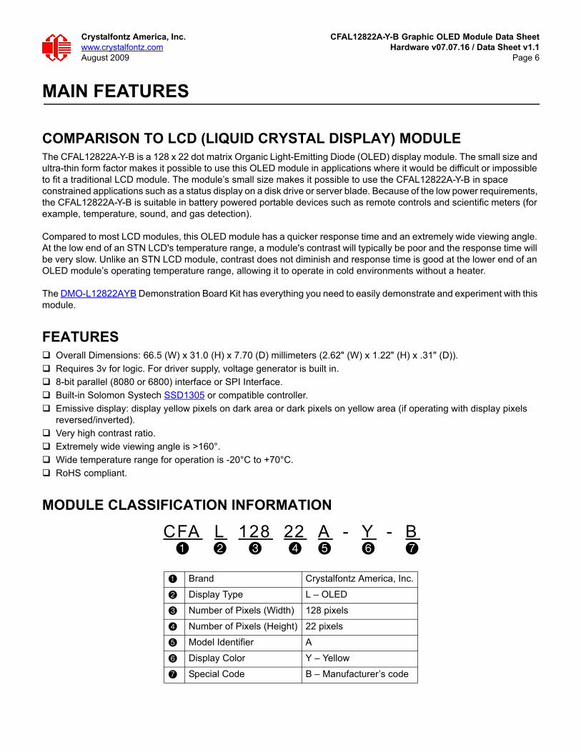
MODULE CLASSIFICATION INFORMATION
CFA L 128 22 A - Y - B
Brand Crystalfontz America, Inc.
Display Type L – OLED
Number of Pixels (Width) 128 pixels
Number of Pixels (Height) 22 pixels
Model Identifier A
Display Color Y – Yellow
Special Code B – Manufacturer’s code
Crystalfontz America, Inc. CFAL12822A-Y-B Graphic OLED Module Data Sheetwww.crystalfontz.com Hardware v07.07.16 / Data Sheet v1.1August 2009 Page 7
MECHANICAL SPECIFICATIONS
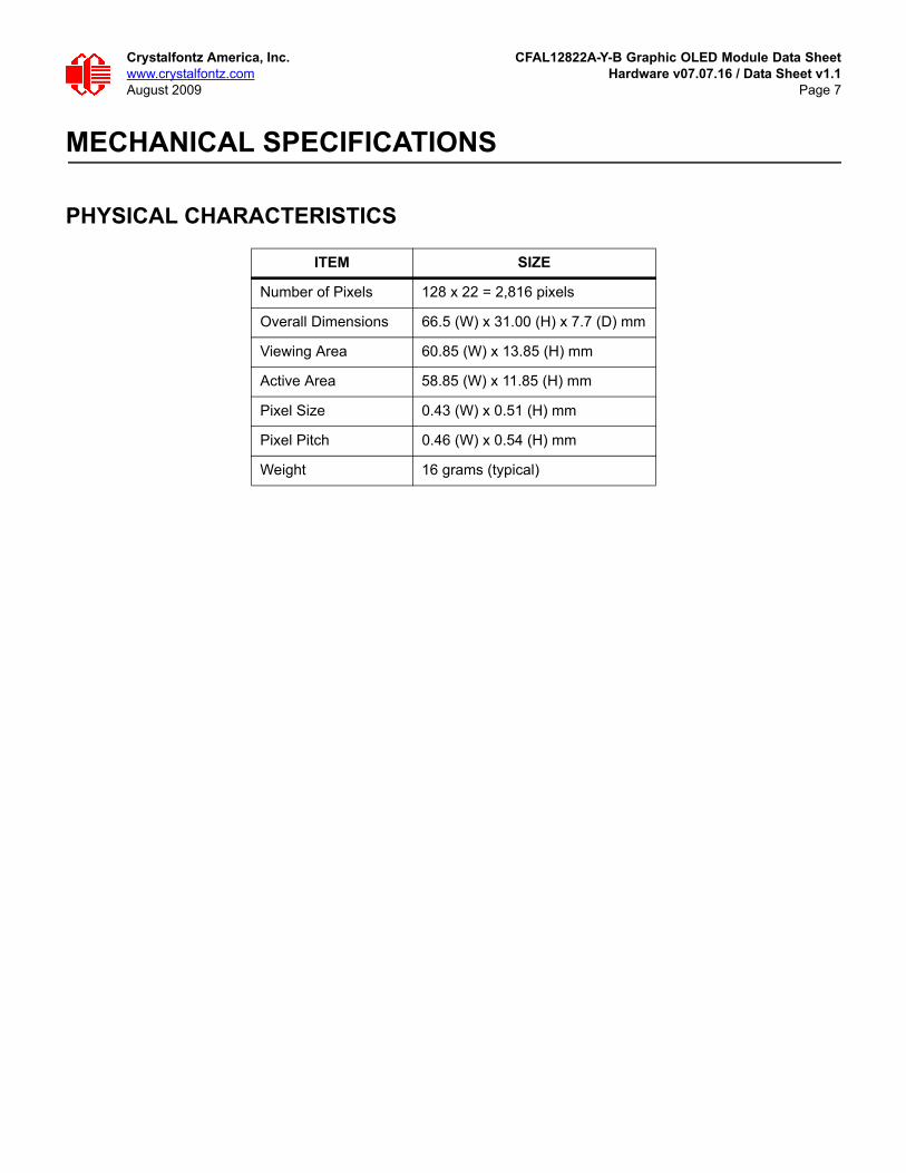
PHYSICAL CHARACTERISTICS
ITEM SIZE
Number of Pixels 128 x 22 = 2,816 pixels
Overall Dimensions 66.5 (W) x 31.00 (H) x 7.7 (D) mm
Viewing Area 60.85 (W) x 13.85 (H) mm
Active Area 58.85 (W) x 11.85 (H) mm
Pixel Size 0.43 (W) x 0.51 (H) mm
Pixel Pitch 0.46 (W) x 0.54 (H) mm
Weight 16 grams (typical)
Crystalfontz America, Inc. CFAL12822A-Y-B Graphic OLED Module Data Sheetwww.crystalfontz.com Hardware v07.07.16 / Data Sheet v1.1August 2009 Page 8
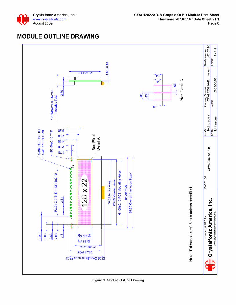
MODULE OUTLINE DRAWING
Figure 1. Module Outline Drawing
128
x 22
.43
.46
.51
.54
.03
.03
P2.
54 X
(18-
1) =
43.
18±0
.10
2.54
18-Ø
0.89
±0.1
0 P
TH18
-Ø1.
52±0
.10
Pad
61.0
0±0.
10 P
CB
Mou
ntin
g H
oles
66.2
0 P
CB
58.8
5 A
ctiv
e A
rea
60.8
5 V
iew
ing
Are
a
66.5
0 O
vera
ll ( I
nclu
des
Bez
el)
11.85 AA
13.85 VA
25.00 Bezel
2.50
1.75
4.95
7.20
8.20
.15
2.60
2.68
3.68
11.5
1
3.70
1.00
±0.1
0
See
Pix
elD
etai
l A
Pix
el D
etai
l A
29.35 PCB
7.70
Max
imum
Ove
rall
(Inc
lude
s Ta
b)
118
Ø2.
60±0
.10
TYP
32.25 Overall (Includes FPC)
29.35 PCB
ww
w.c
ryst
alfo
ntz.
com
/pro
duct
s/C
ryst
alfo
ntz
Am
eric
a, In
c.S
cale
:
Uni
ts:
copy
right
© 2
009
byD
raw
ing
Num
ber:
Dat
e:
Har
dwar
e R
ev.:
She
et:
Par
t No.
(s):
of
CFA
L128
22A
-Y-B
2009
/08/
06
Not
to s
cale
Mill
imet
ers
CFA
L128
22A
-B_m
aste
rv0
7.07
.16
11
Not
e: T
oler
ance
is ±
0.3
mm
unl
ess
spec
ified
.
Crystalfontz America, Inc. CFAL12822A-Y-B Graphic OLED Module Data Sheetwww.crystalfontz.com Hardware v07.07.16 / Data Sheet v1.1August 2009 Page 9
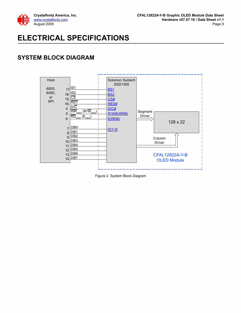
ELECTRICAL SPECIFICATIONS
SYSTEM BLOCK DIAGRAM
Figure 2. System Block Diagram
128 x 22
Host
6800,8080,
orSPI
DB0
Solomon SystechSSD1305
SegmentDriver
ColumnDriver
7 8 91011121314
CS15RST16D/C 4WR8080 (R/W6800) 5RD8080 (E6800) 6
IS218
IS1 17
DB1DB2DB3DB4DB5DB6DB7
CFAL12822A-Y-BOLED Module
D[7-0]
CS#RES#D/C#R/W#(WR#)E(RD#)
BS2BS1
Crystalfontz America, Inc. CFAL12822A-Y-B Graphic OLED Module Data Sheetwww.crystalfontz.com Hardware v07.07.16 / Data Sheet v1.1August 2009 Page 10
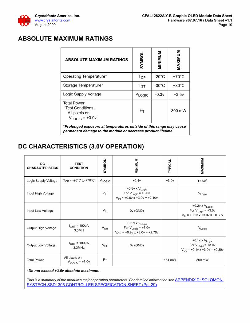
ABSOLUTE MAXIMUM RATINGS
DC CHARACTERISTICS (3.0V OPERATION)
ABSOLUTE MAXIMUM RATINGS
SY
MB
OL
MIN
IMU
M
MA
XIM
UM
Operating Temperature* TOP -20°C +70°C
Storage Temperature* TST -30°C +80°C
Logic Supply Voltage VLOGIC -0.3v +3.5v
Total Power Test Conditions: All pixels on VLOGIC = +3.0v
PT 300 mW
*Prolonged exposure at temperatures outside of this range may cause permanent damage to the module or decrease product lifetime.
DCCHARACTERISTICS
TESTCONDITION
SY
MB
OL
MIN
IMU
M
TY
PIC
AL
MA
XIM
UM
Logic Supply Voltage TOP = -20°C to +70°C VLOGIC +2.4v +3.0v +3.5v1
Input High Voltage VIH
+0.8v x VLogic
For VLogic = +3.0v
VIH = +0.8v x +3.0v = +2.40v
VLogic
Input Low Voltage VIL 0v (GND)
+0.2v x VLogic
For VLogic = +3.0v
VIL = +0.2v x +3.0v = +0.60v
Output High VoltageIOUT = 100µA
3.3MHVOH
+0.9v x VLogic
For VLogic = +3.0v
VOH = +0.9v x +3.0v = +2.70v
VLogic
Output Low VoltageIOUT = 100µA
3.3MHzVOL 0v (GND)
+0.1v x VLogic
For VLogic = +3.0v
VOL = +0.1v x +3.0v = +0.30v
Total Power All pixels on VLOGIC = +3.0v
PT 154 mW 300 mW
1Do not exceed +3.5v absolute maximum.
This is a summary of the module’s major operating parameters. For detailed information see APPENDIX D: SOLOMON SYSTECH SSD1305 CONTROLLER SPECIFICATION SHEET (Pg. 29).
Crystalfontz America, Inc. CFAL12822A-Y-B Graphic OLED Module Data Sheetwww.crystalfontz.com Hardware v07.07.16 / Data Sheet v1.1August 2009 Page 11
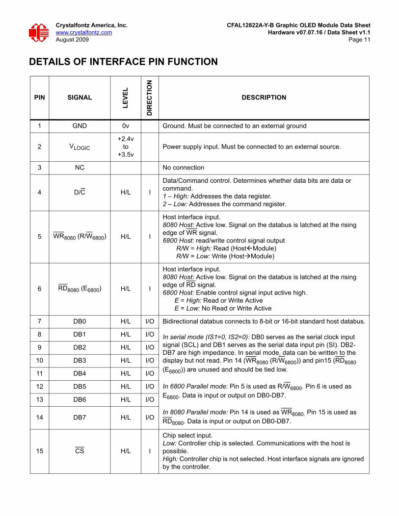
DETAILS OF INTERFACE PIN FUNCTION
PIN SIGNAL
LE
VE
L
DIR
EC
TIO
N
DESCRIPTION
1 GND 0v Ground. Must be connected to an external ground
2 VLOGIC
+2.4vto
+3.5vPower supply input. Must be connected to an external source.
3 NC No connection
4 D/C H/L I
Data/Command control. Determines whether data bits are data or command.1 – High: Addresses the data register.2 – Low: Addresses the command register.
5 WR8080 (R/W6800) H/L I
Host interface input.8080 Host: Active low. Signal on the databus is latched at the rising edge of WR signal.6800 Host: read/write control signal output
R/W = High: Read (HostModule) R/W = Low: Write (HostModule)
6 RD8080 (E6800) H/L I
Host interface input.8080 Host: Active low. Signal on the databus is latched at the rising edge of RD signal. 6800 Host: Enable control signal input active high.
E = High: Read or Write ActiveE = Low: No Read or Write Active
7 DB0 H/L I/O Bidirectional databus connects to 8-bit or 16-bit standard host databus.
In serial mode (IS1=0, IS2=0): DB0 serves as the serial clock input signal (SCL) and DB1 serves as the serial data input pin (SI). DB2-DB7 are high impedance. In serial mode, data can be written to the display but not read. Pin 14 (WR8080 (R/W6800)) and pin15 (RD8080 (E6800)) are unused and should be tied low.
In 6800 Parallel mode: Pin 5 is used as R/W6800. Pin 6 is used as E6800. Data is input or output on DB0-DB7.
In 8080 Parallel mode: Pin 14 is used as WR8080. Pin 15 is used as RD8080. Data is input or output on DB0-DB7.
8 DB1 H/L I/O
9 DB2 H/L I/O
10 DB3 H/L I/O
11 DB4 H/L I/O
12 DB5 H/L I/O
13 DB6 H/L I/O
14 DB7 H/L I/O
15 CS H/L I
Chip select input.Low: Controller chip is selected. Communications with the host is possible.High: Controller chip is not selected. Host interface signals are ignored by the controller.
Crystalfontz America, Inc. CFAL12822A-Y-B Graphic OLED Module Data Sheetwww.crystalfontz.com Hardware v07.07.16 / Data Sheet v1.1August 2009 Page 12
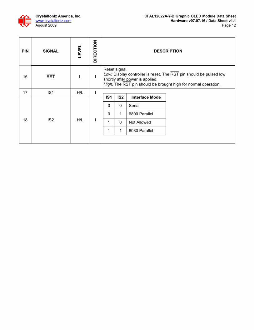
16 RST L I
Reset signal.Low: Display controller is reset. The RST pin should be pulsed low shortly after power is applied.High: The RST pin should be brought high for normal operation.
17 IS1 H/L I
18 IS2 H/L I
PIN SIGNAL
LE
VE
L
DIR
EC
TIO
N
DESCRIPTION
IS1 IS2 Interface Mode
0 0 Serial
0 1 6800 Parallel
1 0 Not Allowed
1 1 8080 Parallel
Crystalfontz America, Inc. CFAL12822A-Y-B Graphic OLED Module Data Sheetwww.crystalfontz.com Hardware v07.07.16 / Data Sheet v1.1August 2009 Page 13
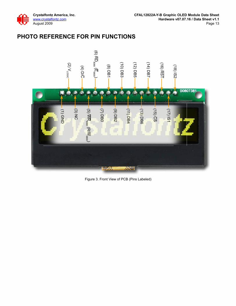
PHOTO REFERENCE FOR PIN FUNCTIONS
Figure 3. Front View of PCB (Pins Labeled)
(14) DB
7
(4) D/C
(2) VLO
GIC
(7) DB
0
(3) NC
(1) GN
D
(11) DB
4
(13) DB
6
(12) DB
5
(18) IS2
(15) CS
(16) RS
T
(17) IS1
(8) DB
1
(9) DB
2
(10) DB
3
(5) WR
8080 (R/W
6800 )
(6) RD
8080 (E6800 )
Crystalfontz America, Inc. CFAL12822A-Y-B Graphic OLED Module Data Sheetwww.crystalfontz.com Hardware v07.07.16 / Data Sheet v1.1August 2009 Page 14
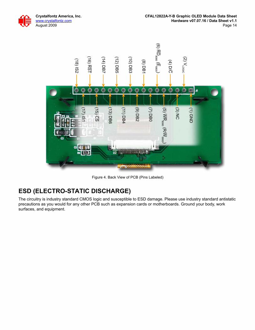
Figure 4. Back View of PCB (Pins Labeled)
ESD (ELECTRO-STATIC DISCHARGE)The circuitry is industry standard CMOS logic and susceptible to ESD damage. Please use industry standard antistatic precautions as you would for any other PCB such as expansion cards or motherboards. Ground your body, work surfaces, and equipment.
(8) DB
1
(14) DB
7
(18) IS2
(12) DB
5
(10) DB
3
(7) DB
0
(13) DB
6
(11) DB
4
(9) DB
2
(3) NC
(17) IS1
(15) CS
(4) D/C
(2) VLO
GIC
(1) GN
D
(16) RS
T
(5) WR
8080 (R/W
6800 )(6) R
D8080 (E
6800 )
Crystalfontz America, Inc. CFAL12822A-Y-B Graphic OLED Module Data Sheetwww.crystalfontz.com Hardware v07.07.16 / Data Sheet v1.1August 2009 Page 15
OPTICAL SPECIFICATIONS
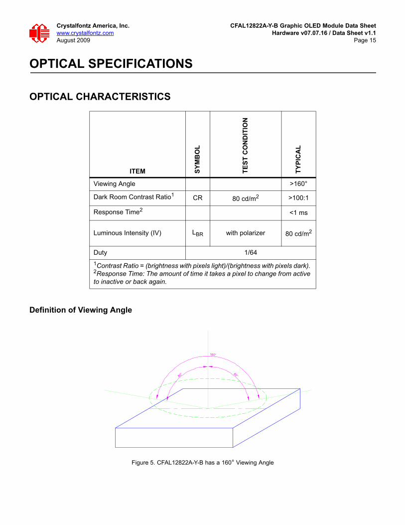
OPTICAL CHARACTERISTICS
Definition of Viewing Angle
Figure 5. CFAL12822A-Y-B has a 160° Viewing Angle
ITEM SY
MB
OL
TE
ST
CO
ND
ITIO
N
TY
PIC
AL
Viewing Angle >160°
Dark Room Contrast Ratio1 CR 80 cd/m2 >100:1
Response Time2 <1 ms
Luminous Intensity (IV) LBR with polarizer 80 cd/m2
Duty 1/64
1Contrast Ratio = (brightness with pixels light)/(brightness with pixels dark). 2Response Time: The amount of time it takes a pixel to change from active to inactive or back again.
80°80°
160°
Crystalfontz America, Inc. CFAL12822A-Y-B Graphic OLED Module Data Sheetwww.crystalfontz.com Hardware v07.07.16 / Data Sheet v1.1August 2009 Page 16
OLED CONTROLLER INTERFACE
This module uses a Solomon Systech SSD1305 controller. For your reference, we added APPENDIX D: SOLOMON SYSTECH SSD1305 CONTROLLER SPECIFICATION SHEET (Pg. 29) to this Data Sheet.
MODULE RELIABILITY AND LONGEVITY
MODULE RELIABILITY
OLED displays are an emissive technology. Each pixel is susceptible to dimming based on its individual use (burn-in). Frequently used pixels will dim more quickly than pixels that are not used as often. Please avoid using a bright, static, high-contrast image for a long time. If you want to leave the display powered on, please use scrolling text or alternating images to "wear level" the pixels. To conserve power and display lifetime, turn off or dim the display when it is not in use.
MODULE LONGEVITY (EOL/REPLACEMENT POLICY)Crystalfontz is committed to making all of our modules available for as long as possible. For each module we introduce, we intend to offer it indefinitely. We do not preplan a module's obsolescence. The majority of modules we have introduced are still available.
We recognize that discontinuing a module may cause problems for some customers. However, rapidly changing technologies, component availability, or low customer order levels may force us to discontinue ("End of Life", EOL) a module. For example, we must occasionally discontinue a module when a supplier discontinues a component or a manufacturing process becomes obsolete. When we discontinue a module, we will do our best to find an acceptable replacement module with the same fit, form, and function.
In most situations, you will not notice a difference when comparing a "fit, form, and function" replacement module to the discontinued module. However, sometimes a change in component or process for the replacement module results in a slight variation, perhaps an improvement, over the previous design.
Although the replacement module is still within the stated Data Sheet specifications and tolerances of the discontinued module, changes may require modification to your circuit and/or firmware. Possible changes include:
Controller. A new controller may require minor changes in your code.
Component tolerances. Module components have manufacturing tolerances. In extreme cases, the tolerance stack can change the visual or operating characteristics.
AVERAGEBRIGHTNESS
SPECIFICATION
80 cd/m2 Brightness will be >50% of a new module’s initial brightness for at least 10,000 hours of operation.
40 cd/m2 20,000 hours.
Test Condition: 25°C.

Crystalfontz America, Inc. CFAL12822A-Y-B Graphic OLED Module Data Sheetwww.crystalfontz.com Hardware v07.07.16 / Data Sheet v1.1August 2009 Page 17
Please understand that we avoid changing a module whenever possible; we only discontinue a module if we have no other option. We will post Part Change Notices on the product's webpage as soon as possible. If interested, you can subscribe to future part change notifications.
CARE AND HANDLING PRECAUTIONS
For optimum operation of the module and to prolong its life, please follow the precautions below.
ESD (ELECTRO-STATIC DISCHARGE)The circuitry is industry standard CMOS logic and susceptible to ESD damage. Please use industry standard antistatic precautions as you would for any other PCB such as expansion cards or motherboards. Ground your body, work surfaces, and equipment.
DESIGN AND MOUNTING The exposed surface of the “glass” is actually a polarizer laminated on top of the glass.To protect the soft plastic
polarizer from damage, the module ships with a protective film over the polarizer. Please peel off the protective film slowly. Peeling off the protective film abruptly may generate static electricity.
The polarizer is made out of soft plastic and is easily scratched or damaged. When handling the module, avoid touching the polarizer. Finger oils are difficult to remove.
To protect the soft plastic polarizer from damage, place a transparent plate (for example, acrylic, polycarbonate, or glass) in front of the module, leaving a small gap between the plate and the display surface. We use GE HP-92 Lexan, which is readily available and works well.
Do not disassemble or modify the module.
Do not modify the tab of the metal holder or make connections to it.
Do not reverse polarity to the power supply connections. Reversing polarity will immediately ruin the module.
Use care to keep the exposed terminals clean. Contamination, including fingerprints may make soldering difficult, and the reliability of the soldered connection poor.
For prototype work, hand soldering may be acceptable. Preset soldering iron to <260°C. Do not apply heat for more than 3 to 4 seconds.
AVOID SHOCK, IMPACT, TORQUE, OR TENSION Do not expose the module to strong mechanical shock, impact, torque, or tension.
Do not drop, toss, bend, or twist the module.
Do not place weight or pressure on the module.
CLEANINGThe polarizer (laminated to the glass) is soft plastic. The soft plastic is easily scratched or damaged. Be very careful when you clean the polarizer.
Do not clean the polarizer with liquids. Do not wipe the polarizer with any type of cloth or swab (for example, Q-tips).
Use the removable protective film to remove smudges (for example, fingerprints) and any foreign matter. If you no longer have the protective film, use standard transparent office tape (for example, Scotch® brand “Crystal Clear Tape”). If the polarizer is dusty, you may carefully blow it off with clean, dry, oil-free compressed air.

Crystalfontz America, Inc. CFAL12822A-Y-B Graphic OLED Module Data Sheetwww.crystalfontz.com Hardware v07.07.16 / Data Sheet v1.1August 2009 Page 18
OPERATION We do not recommend connecting this module to a PC's parallel port as an "end product.” This module is not
"user friendly" and connecting it to a PC's parallel port is often difficult, frustrating, and can result in a "dead" display due to mishandling. For more information, see our forum thread at http://www.crystalfontz.com/forum/showthread.php?s=&threadid=3257.
Your circuit should be designed to protect the module from ESD and power supply transients.
Observe the operating temperature limitations: from -20°C minimum to +70°C maximum with minimal fluctuations. Operation outside of these limits may shorten the life and/or harm the display.
Operate away from dust, moisture, and direct sunlight.
STORAGE AND RECYCLING Store in an ESD-approved container away from dust, moisture, and direct sunlight, fluorescent lamps, or any
ultraviolet ray.
Observe the storage temperature limitations: from -30°C minimum to +80°C maximum with minimal fluctuations. Rapid temperature changes can cause moisture to form, resulting in permanent damage.
Do not allow weight to be placed on the modules while they are in storage.
Please recycle your outdated Crystalfontz modules at an approved facility.
Crystalfontz America, Inc. CFAL12822A-Y-B Graphic OLED Module Data Sheetwww.crystalfontz.com Hardware v07.07.16 / Data Sheet v1.1August 2009 Page 19
APPENDIX A: QUALITY ASSURANCE STANDARDS
INSPECTION CONDITIONS Environment
Temperature: 25±5°C
Humidity: 30~85% RH (noncondensing)
For visual inspection of active display area
Source lighting: two 20-Watt or one 40-Watt fluorescent light
Display adjusted for best contrast
Viewing distance: 30±5 cm (about 12 inches)
Viewing angle: inspect at 45° angle of vertical line right and left, top and bottom
COLOR DEFINITIONSWe try to describe the appearance of our modules as accurately as possible. For the photos, we adjust for optimal appearance. Actual display appearance may vary due to (1) different operating conditions, (2) small variations of component tolerances, (3) inaccuracies of our camera, (4) color interpretation of the photos on your monitor, and/or (5) personal differences in the perception of color.
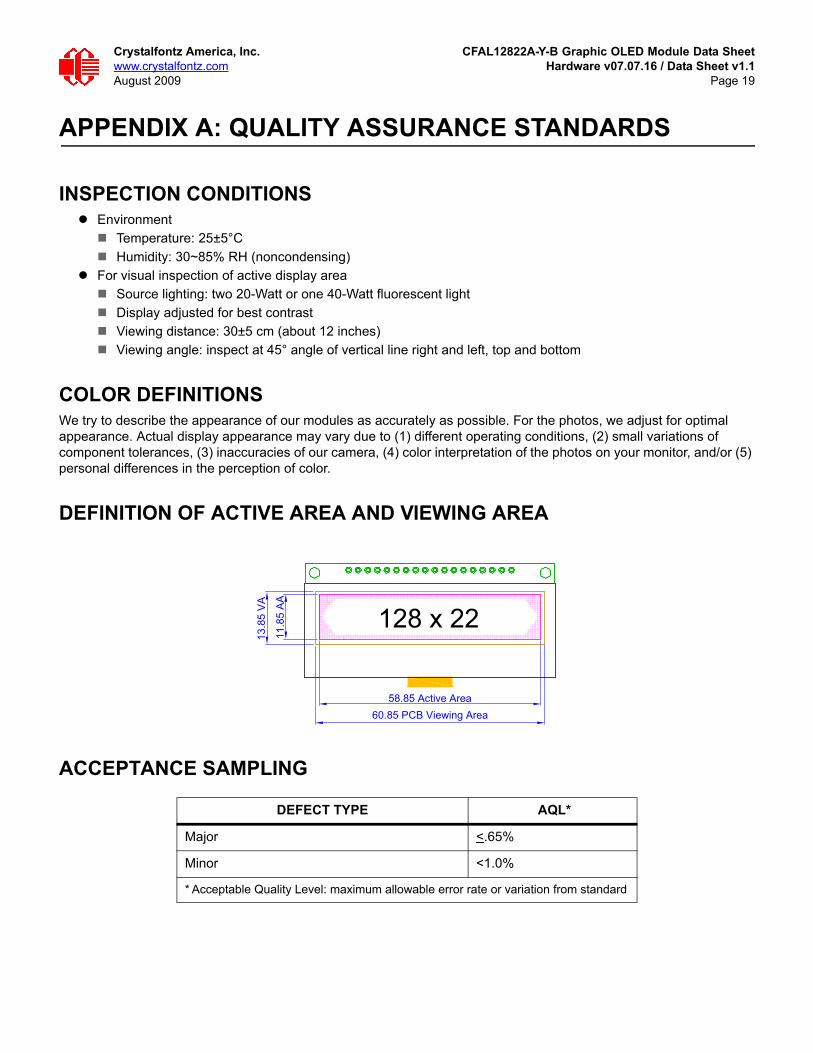
DEFINITION OF ACTIVE AREA AND VIEWING AREA
ACCEPTANCE SAMPLING
DEFECT TYPE AQL*
Major <.65%
Minor <1.0%
* Acceptable Quality Level: maximum allowable error rate or variation from standard
60.85 PCB Viewing Area58.85 Active Area
11.8
5 A
A
13.8
5 V
A
128 x 22
Crystalfontz America, Inc. CFAL12822A-Y-B Graphic OLED Module Data Sheetwww.crystalfontz.com Hardware v07.07.16 / Data Sheet v1.1August 2009 Page 20
DEFECTS CLASSIFICATIONDefects are defined as:
Major Defect: results in failure or substantially reduces usability of unit for its intended purpose.
Minor Defect: deviates from standards but is not likely to reduce usability for its intended purpose.
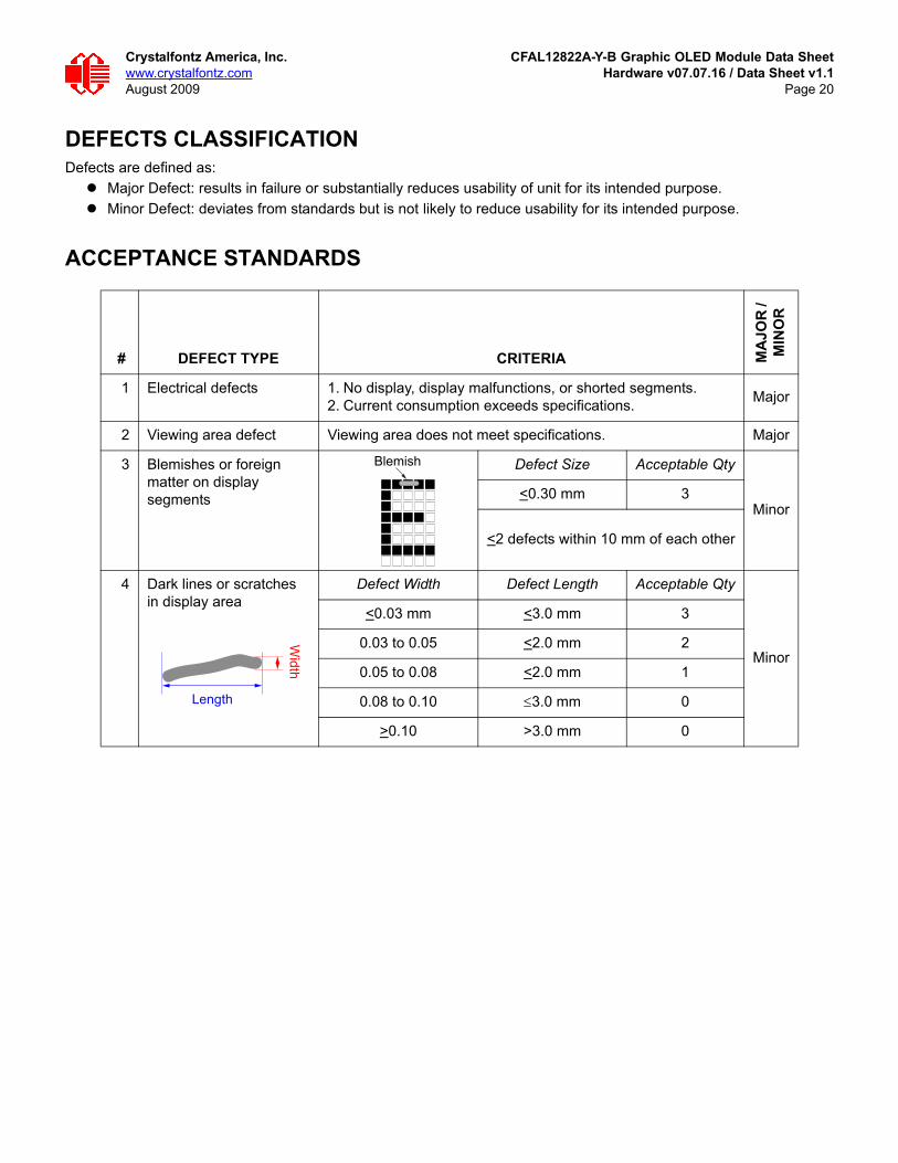
ACCEPTANCE STANDARDS
# DEFECT TYPE CRITERIA MA
JO
R /
MIN
OR
1 Electrical defects 1. No display, display malfunctions, or shorted segments.2. Current consumption exceeds specifications.
Major
2 Viewing area defect Viewing area does not meet specifications. Major
3 Blemishes or foreign matter on displaysegments
Defect Size Acceptable Qty
Minor<0.30 mm 3
<2 defects within 10 mm of each other
4 Dark lines or scratches in display area
Defect Width Defect Length Acceptable Qty
Minor
<0.03 mm <3.0 mm 3
0.03 to 0.05 <2.0 mm 2
0.05 to 0.08 <2.0 mm 1
0.08 to 0.10 3.0 mm 0
>0.10 >3.0 mm 0
Blemish
Width
Length
Crystalfontz America, Inc. CFAL12822A-Y-B Graphic OLED Module Data Sheetwww.crystalfontz.com Hardware v07.07.16 / Data Sheet v1.1August 2009 Page 21
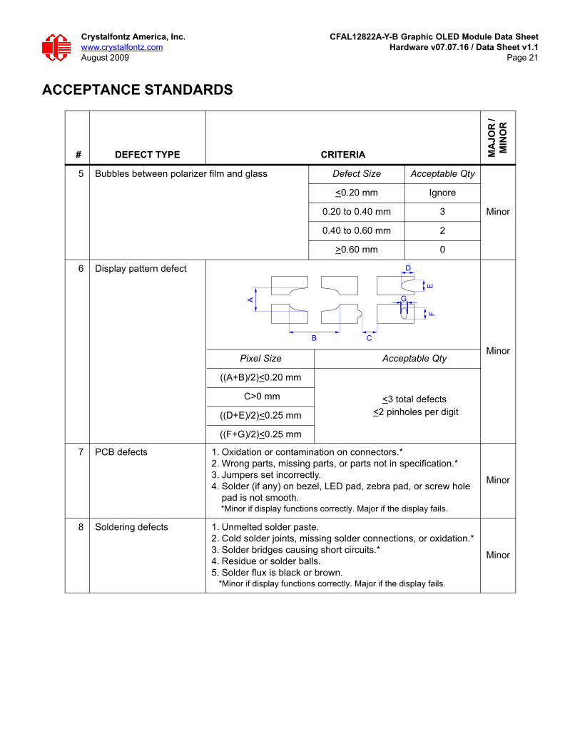
ACCEPTANCE STANDARDS
# DEFECT TYPE CRITERIA MA
JO
R /
MIN
OR
5 Bubbles between polarizer film and glass Defect Size Acceptable Qty
Minor
<0.20 mm Ignore
0.20 to 0.40 mm 3
0.40 to 0.60 mm 2
>0.60 mm 0
6 Display pattern defect
Minor
7 PCB defects 1. Oxidation or contamination on connectors.*2. Wrong parts, missing parts, or parts not in specification.*3. Jumpers set incorrectly.4. Solder (if any) on bezel, LED pad, zebra pad, or screw hole
pad is not smooth. *Minor if display functions correctly. Major if the display fails.
Minor
8 Soldering defects 1. Unmelted solder paste.2. Cold solder joints, missing solder connections, or oxidation.*3. Solder bridges causing short circuits.*4. Residue or solder balls.5. Solder flux is black or brown. *Minor if display functions correctly. Major if the display fails.
Minor
D
A
B C
EF
G
Pixel Size Acceptable Qty
((A+B)/2)<0.20 mm
<3 total defects <2pinholes per digit
C>0 mm
((D+E)/2)<0.25 mm
((F+G)/2)<0.25 mm
Crystalfontz America, Inc. CFAL12822A-Y-B Graphic OLED Module Data Sheetwww.crystalfontz.com Hardware v07.07.16 / Data Sheet v1.1August 2009 Page 22
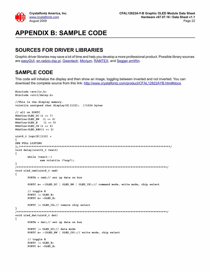
APPENDIX B: SAMPLE CODE
SOURCES FOR DRIVER LIBRARIESGraphic driver libraries may save a lot of time and help you develop a more professional product. Possible library sources are easyGUI, en.radzio.dxp.pl, Gwentech, Micriµm, RAMTEX, and Segger emWin.
SAMPLE CODEThis code will initialize the display and then show an image, toggling between inverted and not inverted. You can download the complete source from this link: http://www.crystalfontz.com/product/CFAL12822AYB.html#docs.
#include <avr/io.h> #include <util/delay.h>
//This is the display memory.volatile unsigned char display[8][132]; //1024 bytes
// all on PORTC#define OLED_DC (1 << 7)#define OLED_RW (1 << 6)#define OLED_E (1 << 5)#define OLED_CS (1 << 4)#define OLED_RES(1 << 2)
uint8_t logo[8][132] ={SEE FULL LISTING};/*******************************************************************************************/void delay(uint32_t twait){
while (twait--)asm volatile ("nop");
}/*******************************************************************************************/void oled_cmd(uint8_t cmd){
PORTA = cmd;// set up data on bus
PORTC &= ~(OLED_DC | OLED_RW | OLED_CS);// command mode, write mode, chip select
// toggle EPORTC |= OLED_E;PORTC &= ~OLED_E;
PORTC |= OLED_CS;// remove chip select}/*******************************************************************************************/void oled_dat(uint8_t dat){
PORTA = dat;// set up data on bus
PORTC |= OLED_DC;// data modePORTC &= ~(OLED_RW | OLED_CS);// write mode, chip select
// toggle EPORTC |= OLED_E;PORTC &= ~OLED_E;
Crystalfontz America, Inc. CFAL12822A-Y-B Graphic OLED Module Data Sheetwww.crystalfontz.com Hardware v07.07.16 / Data Sheet v1.1August 2009 Page 23
PORTC |= OLED_CS;// remove chip select}/*******************************************************************************************/void oled_clr(uint8_t color){
int i,p;
oled_cmd(0x40);
for (p=0;p<8;p++) // pages{
oled_cmd(0xb0 + p);oled_cmd(0x10);oled_cmd(0x00);for (i=0;i<132;i++)// ?????{
oled_dat(color);}
}}/*******************************************************************************************/typedef uint8_t bitmap_t[8][132];
void bmp(bitmap_t b){
int i,j, index;
for (j=0;j<8;j++){
oled_cmd(0xB0+j); oled_cmd(0x04); oled_cmd(0x10);
for(i=0;i<128;i++) oled_dat( b[j][i] );
}}/*******************************************************************************************/int main( void ){
PORTD = 0; // all off
DDRD |= (1<<3);// VPP output
DDRA = 0xFF;
//6800 modePORTC = 0b11011110;
DDRC = 0xFE;
delay(20000L);
PORTC &= ~OLED_RES;delay(10000);PORTC |= OLED_RES;
delay(20000);
// enable VPPPORTD |= (1<<3);
delay(200000L);
oled_cmd(0xae); //Set Display ON/OFF
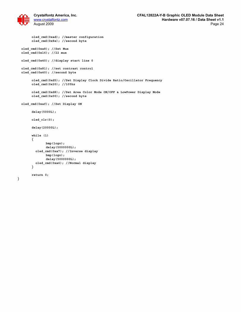
Crystalfontz America, Inc. CFAL12822A-Y-B Graphic OLED Module Data Sheetwww.crystalfontz.com Hardware v07.07.16 / Data Sheet v1.1August 2009 Page 24
oled_cmd(0xad); //master configurationoled_cmd(0x8e); //second byte
oled_cmd(0xa8); //Set Mux oled_cmd(0x16); //22 mux
oled_cmd(0x40); //display start line 0
oled_cmd(0x81); //set contrast control oled_cmd(0x40); //second byte
oled_cmd(0xd5); //Set Display Clock Divide Ratio/Oscillator Frequencyoled_cmd(0x20); //105hz
oled_cmd(0xd8); //Set Area Color Mode ON/OFF & LowPower Display Modeoled_cmd(0x00); //second byte
oled_cmd(0xaf); //Set Display ON
delay(5000L);
oled_clr(0);
delay(20000L);
while (1){
bmp(logo);delay(5000000L);
oled_cmd(0xa7); //Inverse displaybmp(logo);delay(5000000L);
oled_cmd(0xa6); //Normal display}
return 0;}
Crystalfontz America, Inc. CFAL12822A-Y-B Graphic OLED Module Data Sheetwww.crystalfontz.com Hardware v07.07.16 / Data Sheet v1.1August 2009 Page 25
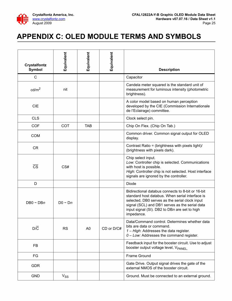
APPENDIX C: OLED MODULE TERMS AND SYMBOLS
CrystalfontzSymbol E
qu
iva
len
t
Eq
uiv
ale
nt
Eq
uiv
ale
nt
Description
C Capacitor
cd/m2 nitCandela meter squared is the standard unit of measurement for luminous intensity (photometric brightness).
CIEA color model based on human perception developed by the CIE (Commission Internationale de l’Eclairage) committee.
CLS Clock select pin.
COF COT TAB Chip On Flex. (Chip On Tab.)
COMCommon driver. Common signal output for OLED display.
CRContrast Ratio = (brightness with pixels light)/(brightness with pixels dark).
CS CS#
Chip select input.Low: Controller chip is selected. Communications with host is possible.High: Controller chip is not selected. Host interface signals are ignored by the controller.
D Diode
DB0 ~ DBn D0 ~ Dn
Bidirectional databus connects to 8-bit or 16-bit standard host databus. When serial interface is selected, DB0 serves as the serial clock input signal (SCL) and DB1 serves as the serial data input signal (SI). DB2 to DBn are set to high impedance.
D/C RS A0 CD or D/C#
Data/Command control. Determines whether data bits are data or command.1 – High: Addresses the data register.0 – Low: Addresses the command register.
FBFeedback input for the booster circuit. Use to adjust booster output voltage level, VPANEL.
FG Frame Ground
GDRGate Drive. Output signal drives the gate of the external NMOS of the booster circuit.
GND VSS Ground. Must be connected to an external ground.
Crystalfontz America, Inc. CFAL12822A-Y-B Graphic OLED Module Data Sheetwww.crystalfontz.com Hardware v07.07.16 / Data Sheet v1.1August 2009 Page 26
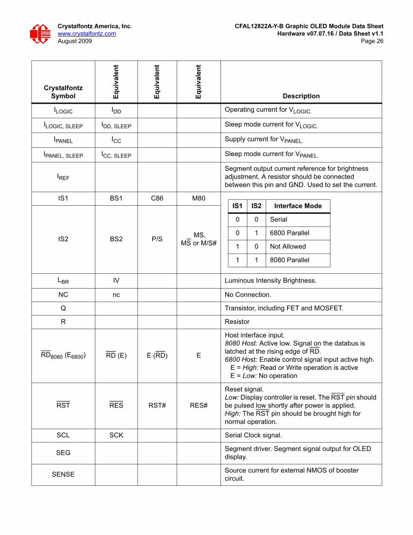
ILOGIC IDD Operating current for VLOGIC.
ILOGIC, SLEEP IDD, SLEEP Sleep mode current for VLOGIC.
IPANEL ICC Supply current for VPANEL.
IPANEL, SLEEP ICC, SLEEP Sleep mode current for VPANEL.
IREF
Segment output current reference for brightness adjustment. A resistor should be connected between this pin and GND. Used to set the current.
IS1 BS1 C86 M80
IS2 BS2 P/S MS,
MS or M/S#
LBR IV Luminous Intensity Brightness.
NC nc No Connection.
Q Transistor, including FET and MOSFET.
R Resistor
RD8080 (E6800) RD (E) E (RD) E
Host interface input.8080 Host: Active low. Signal on the databus is latched at the rising edge of RD. 6800 Host: Enable control signal input active high. E = High: Read or Write operation is active E = Low: No operation
RST RES RST# RES#
Reset signal.Low: Display controller is reset. The RST pin should be pulsed low shortly after power is applied.High: The RST pin should be brought high for normal operation.
SCL SCK Serial Clock signal.
SEGSegment driver. Segment signal output for OLED display.
SENSESource current for external NMOS of booster circuit.
CrystalfontzSymbol E
qu
ival
ent
Eq
uiv
alen
t
Eq
uiv
alen
t
Description
IS1 IS2 Interface Mode
0 0 Serial
0 1 6800 Parallel
1 0 Not Allowed
1 1 8080 Parallel
Crystalfontz America, Inc. CFAL12822A-Y-B Graphic OLED Module Data Sheetwww.crystalfontz.com Hardware v07.07.16 / Data Sheet v1.1August 2009 Page 27
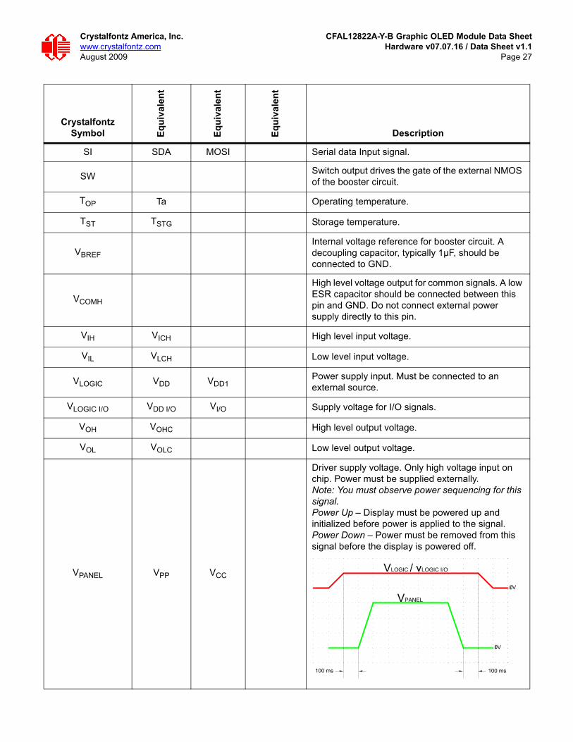
SI SDA MOSI Serial data Input signal.
SWSwitch output drives the gate of the external NMOS of the booster circuit.
TOP Ta Operating temperature.
TST TSTG Storage temperature.
VBREF
Internal voltage reference for booster circuit. A decoupling capacitor, typically 1µF, should be connected to GND.
VCOMH
High level voltage output for common signals. A low ESR capacitor should be connected between this pin and GND. Do not connect external power supply directly to this pin.
VIH VICH High level input voltage.
VIL VLCH Low level input voltage.
VLOGIC VDD VDD1Power supply input. Must be connected to an external source.
VLOGIC I/O VDD I/O VI/O Supply voltage for I/O signals.
VOH VOHC High level output voltage.
VOL VOLC Low level output voltage.
VPANEL VPP VCC
Driver supply voltage. Only high voltage input on chip. Power must be supplied externally.Note: You must observe power sequencing for this signal.Power Up – Display must be powered up and initialized before power is applied to the signal.Power Down – Power must be removed from this signal before the display is powered off.
CrystalfontzSymbol E
qu
ival
ent
Eq
uiv
alen
t
Eq
uiv
alen
t
Description
0/ V
0/ V
VLOGIC / vLOGIC I/O
VPANEL
100 ms 100 ms
Crystalfontz America, Inc. CFAL12822A-Y-B Graphic OLED Module Data Sheetwww.crystalfontz.com Hardware v07.07.16 / Data Sheet v1.1August 2009 Page 28
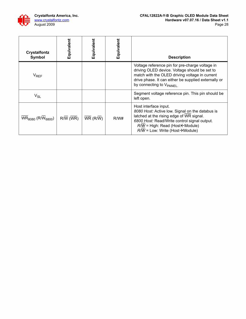
VREF
Voltage reference pin for pre-charge voltage in driving OLED device. Voltage should be set to match with the OLED driving voltage in current drive phase. It can either be supplied externally or by connecting to VPANEL.
VSLSegment voltage reference pin. This pin should be left open.
WR8080 (R/W6800) R/W (WR) WR (R/W) R/W#
Host interface input.8080 Host: Active low. Signal on the databus is latched at the rising edge of WR signal.6800 Host: Read/Write control signal output. R/W = High: Read (HostModule) R/W = Low: Write (HostModule)
CrystalfontzSymbol E
qu
ival
ent
Eq
uiv
alen
t
Eq
uiv
alen
t
Description

Crystalfontz America, Inc. CFAL12822A-Y-B Graphic OLED Module Data Sheetwww.crystalfontz.com Hardware v07.07.16 / Data Sheet v1.1August 2009 Page 29
APPENDIX D: SOLOMON SYSTECH SSD1305 CONTROLLER SPECIFICATION SHEET
The complete SOLOMON SYSTECH SSD1305 Advance Information 132 x 64 Dot Matrix OLED/PLED Segment/Common Driver with Controller (70 pages) follows.
SOLOMON SYSTECH SEMICONDUCTOR TECHNICAL DATA
This document contains information on a new product. Specifications and information herein are subject to change without notice. http://www.solomon-systech.com SSD1305 Rev 1.9 P 1/70 May 2008 Copyright © 2008 Solomon Systech Limited
SSD1305
Advance Information
132 x 64 Dot Matrix OLED/PLED Segment/Common Driver with Controller
Appendix
Solomon Systech May 2008 P 2/70 Rev 1.9 SSD1305
CONTENTS
1 GENERAL DESCRIPTION.................................................................................................... 7
2 FEATURES ............................................................................................................................... 7
3 ORDERING INFORMATION................................................................................................ 7
4 BLOCK DIAGRAM ................................................................................................................. 8
5 DIE PAD FLOOR PLAN ......................................................................................................... 9
6 PIN ARRANGEMENT .......................................................................................................... 12 6.1 SSD1305T6R1 PIN ASSIGNMENT.........................................................................................................................12 6.2 SSD1305T7R1 PIN ASSIGNMENT.........................................................................................................................14
7 PIN DESCRIPTION............................................................................................................... 16
8 FUNCTIONAL BLOCK DESCRIPTIONS ......................................................................... 18 8.1 MCU INTERFACE SELECTION...............................................................................................................................18 8.1.1 MCU Parallel 6800-series Interface...............................................................................................................18 8.1.2 MCU Parallel 8080-series Interface...............................................................................................................19 8.1.3 MCU Serial Interface......................................................................................................................................21 8.1.4 MCU I2C Interface..........................................................................................................................................21
8.2 COMMAND DECODER ..........................................................................................................................................24 8.3 OSCILLATOR CIRCUIT AND DISPLAY TIME GENERATOR......................................................................................25 8.4 FR SYNCHRONIZATION ........................................................................................................................................26 8.5 RESET CIRCUIT ....................................................................................................................................................26 8.6 SEGMENT DRIVERS / COMMON DRIVERS .............................................................................................................27 8.7 GRAPHIC DISPLAY DATA RAM (GDDRAM)......................................................................................................29 8.8 AREA COLOR DECODER.......................................................................................................................................30 8.9 SEG/COM DRIVING BLOCK ................................................................................................................................31 8.10 POWER ON AND OFF SEQUENCE .........................................................................................................................32
9 COMMAND TABLE.............................................................................................................. 33 9.1 DATA READ / WRITE ...........................................................................................................................................39
10 COMMAND DESCRIPTIONS ............................................................................................. 40 10.1 FUNDAMENTAL COMMAND .................................................................................................................................40 10.1.1 Set Lower Column Start Address for Page Addressing Mode (00h~0Fh) ......................................................40 10.1.2 Set Higher Column Start Address for Page Addressing Mode (10h~1Fh) .....................................................40 10.1.3 Set Memory Addressing Mode (20h)...............................................................................................................40 10.1.4 Set Column Address (21h) ..............................................................................................................................41 10.1.5 Set Page Address (22h)...................................................................................................................................42 10.1.6 Set Display Start Line (40h~7Fh) ...................................................................................................................43 10.1.7 Set Contrast Control for BANK0 (81h)...........................................................................................................43 10.1.8 Set Brightness for Area Color Banks (82h).....................................................................................................43 10.1.9 Set Look Up Table (LUT) (91h) .....................................................................................................................43 10.1.10 Set Bank Color of BANK1 to BANK16 (PAGE0) (92h) ..............................................................................44 10.1.11 Set Bank Color of BANK17 to BANK32 (PAGE0) (93h) ............................................................................44 10.1.12 Set Segment Re-map (A0h/A1h) ..................................................................................................................44 10.1.13 Entire Display ON (A4h/A5h) ...................................................................................................................44 10.1.14 Set Normal/Inverse Display (A6h/A7h).......................................................................................................44 10.1.15 Set Multiplex Ratio (A8h)............................................................................................................................44 10.1.16 Reserved (AAh) ...........................................................................................................................................44 10.1.17 Dim Mode setting (ABh) .............................................................................................................................44 10.1.18 Master Configuration (ADh).......................................................................................................................44
Appendix
SSD1305 Rev 1.9 P 3/70 May 2008 Solomon Systech
10.1.19 Set Display ON/OFF (ACh/AEh/AFh) ........................................................................................................45 10.1.20 Set Page Start Address for Page Addressing Mode (B0h~B7h)..................................................................45 10.1.21 Set COM Output Scan Direction (C0h/C8h)...............................................................................................45 10.1.22 Set Display Offset (D3h) .............................................................................................................................45 10.1.23 Set Display Clock Divide Ratio/ Oscillator Frequency (D5h) ....................................................................48 10.1.24 Set Area Color Mode ON/OFF & Low Power Display Mode (D8h) ..........................................................48 10.1.25 Set Pre-charge Period (D9h) ......................................................................................................................48 10.1.26 Set COM Pins Hardware Configuration (DAh)..........................................................................................49 10.1.27 Set VCOMH Deselect Level (DBh) .................................................................................................................51 10.1.28 Enter Read Modify Write (E0h) ..................................................................................................................51 10.1.29 NOP (E3h) ..................................................................................................................................................52 10.1.30 Exit Read Modify Write (EEh) ....................................................................................................................52 10.1.31 Status register Read ....................................................................................................................................52
10.2 GRAPHIC ACCELERATION COMMAND..................................................................................................................53 10.2.1 Horizontal Scroll Setup (26h/27h) ..................................................................................................................53 10.2.2 Continuous Vertical and Horizontal Scroll Setup (29h/2Ah)..........................................................................54 10.2.3 Deactivate Scroll (2Eh)...................................................................................................................................55 10.2.4 Activate Scroll (2Fh).......................................................................................................................................55 10.2.5 Set Vertical Scroll Area(A3h) .........................................................................................................................56
11 MAXIMUM RATINGS.......................................................................................................... 57
12 DC CHARACTERISTICS..................................................................................................... 58
13 AC CHARACTERISTICS..................................................................................................... 59
14 APPLICATION EXAMPLE.................................................................................................. 64
15 PACKAGE INFORMATION................................................................................................ 65 15.1 SSD1305Z DIE TRAY INFORMATION...................................................................................................................65 15.2 SSD1305T6R1 DETAIL DIMENSION ....................................................................................................................66 15.3 SSD1305T7R1 DETAIL DIMENSION ....................................................................................................................68 15.4 SSD1305Z3 DIE TRAY INFORMATION.................................................................................................................69
Appendix
Solomon Systech May 2008 P 4/70 Rev 1.9 SSD1305
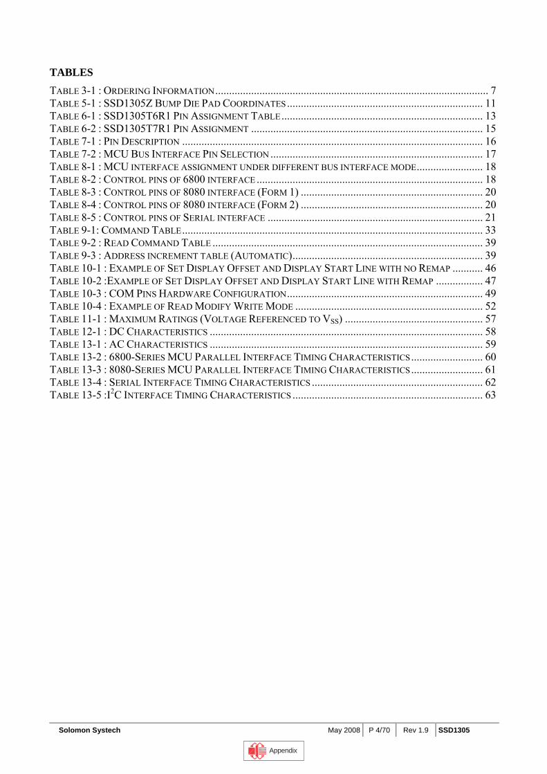
TABLES TABLE 3-1 : ORDERING INFORMATION................................................................................................... 7 TABLE 5-1 : SSD1305Z BUMP DIE PAD COORDINATES....................................................................... 11 TABLE 6-1 : SSD1305T6R1 PIN ASSIGNMENT TABLE......................................................................... 13 TABLE 6-2 : SSD1305T7R1 PIN ASSIGNMENT .................................................................................... 15 TABLE 7-1 : PIN DESCRIPTION ............................................................................................................. 16 TABLE 7-2 : MCU BUS INTERFACE PIN SELECTION ............................................................................. 17 TABLE 8-1 : MCU INTERFACE ASSIGNMENT UNDER DIFFERENT BUS INTERFACE MODE........................ 18 TABLE 8-2 : CONTROL PINS OF 6800 INTERFACE .................................................................................. 18 TABLE 8-3 : CONTROL PINS OF 8080 INTERFACE (FORM 1) .................................................................. 20 TABLE 8-4 : CONTROL PINS OF 8080 INTERFACE (FORM 2) .................................................................. 20 TABLE 8-5 : CONTROL PINS OF SERIAL INTERFACE .............................................................................. 21 TABLE 9-1: COMMAND TABLE............................................................................................................. 33 TABLE 9-2 : READ COMMAND TABLE .................................................................................................. 39 TABLE 9-3 : ADDRESS INCREMENT TABLE (AUTOMATIC)..................................................................... 39 TABLE 10-1 : EXAMPLE OF SET DISPLAY OFFSET AND DISPLAY START LINE WITH NO REMAP ........... 46 TABLE 10-2 :EXAMPLE OF SET DISPLAY OFFSET AND DISPLAY START LINE WITH REMAP ................. 47 TABLE 10-3 : COM PINS HARDWARE CONFIGURATION....................................................................... 49 TABLE 10-4 : EXAMPLE OF READ MODIFY WRITE MODE .................................................................... 52 TABLE 11-1 : MAXIMUM RATINGS (VOLTAGE REFERENCED TO VSS) .................................................. 57 TABLE 12-1 : DC CHARACTERISTICS ................................................................................................... 58 TABLE 13-1 : AC CHARACTERISTICS ................................................................................................... 59 TABLE 13-2 : 6800-SERIES MCU PARALLEL INTERFACE TIMING CHARACTERISTICS.......................... 60 TABLE 13-3 : 8080-SERIES MCU PARALLEL INTERFACE TIMING CHARACTERISTICS.......................... 61 TABLE 13-4 : SERIAL INTERFACE TIMING CHARACTERISTICS .............................................................. 62 TABLE 13-5 :I2C INTERFACE TIMING CHARACTERISTICS ..................................................................... 63
Appendix
SSD1305 Rev 1.9 P 5/70 May 2008 Solomon Systech
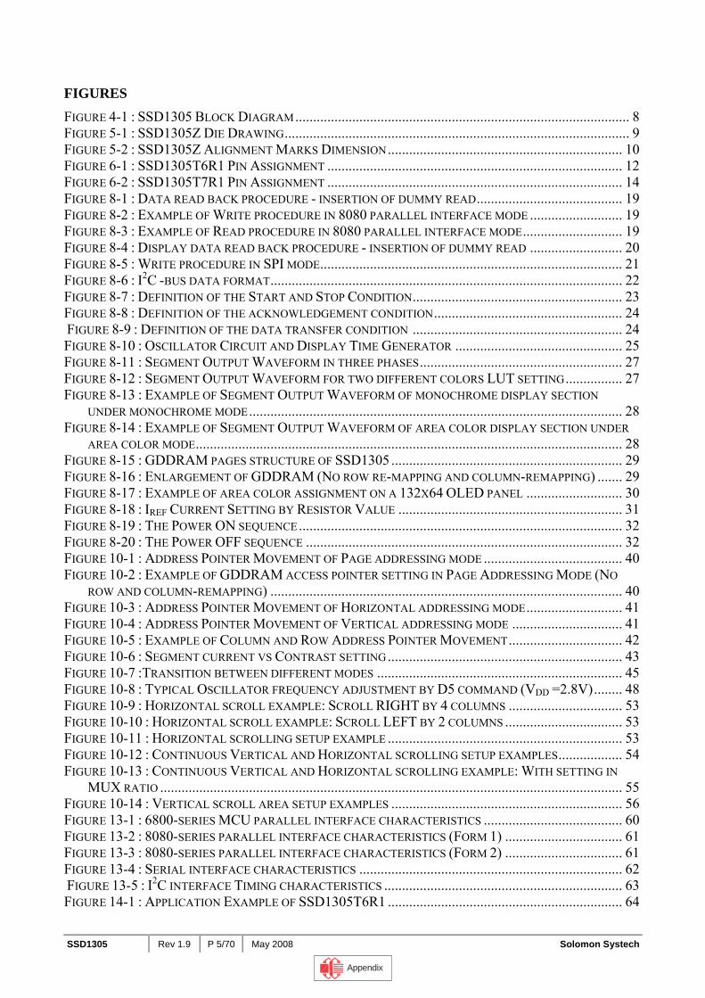
FIGURES FIGURE 4-1 : SSD1305 BLOCK DIAGRAM.............................................................................................. 8 FIGURE 5-1 : SSD1305Z DIE DRAWING................................................................................................. 9 FIGURE 5-2 : SSD1305Z ALIGNMENT MARKS DIMENSION.................................................................. 10 FIGURE 6-1 : SSD1305T6R1 PIN ASSIGNMENT ................................................................................... 12 FIGURE 6-2 : SSD1305T7R1 PIN ASSIGNMENT ................................................................................... 14 FIGURE 8-1 : DATA READ BACK PROCEDURE - INSERTION OF DUMMY READ......................................... 19 FIGURE 8-2 : EXAMPLE OF WRITE PROCEDURE IN 8080 PARALLEL INTERFACE MODE .......................... 19 FIGURE 8-3 : EXAMPLE OF READ PROCEDURE IN 8080 PARALLEL INTERFACE MODE............................ 19 FIGURE 8-4 : DISPLAY DATA READ BACK PROCEDURE - INSERTION OF DUMMY READ .......................... 20 FIGURE 8-5 : WRITE PROCEDURE IN SPI MODE..................................................................................... 21 FIGURE 8-6 : I2C -BUS DATA FORMAT................................................................................................... 22 FIGURE 8-7 : DEFINITION OF THE START AND STOP CONDITION........................................................... 23 FIGURE 8-8 : DEFINITION OF THE ACKNOWLEDGEMENT CONDITION..................................................... 24 FIGURE 8-9 : DEFINITION OF THE DATA TRANSFER CONDITION ........................................................... 24 FIGURE 8-10 : OSCILLATOR CIRCUIT AND DISPLAY TIME GENERATOR ............................................... 25 FIGURE 8-11 : SEGMENT OUTPUT WAVEFORM IN THREE PHASES......................................................... 27 FIGURE 8-12 : SEGMENT OUTPUT WAVEFORM FOR TWO DIFFERENT COLORS LUT SETTING................ 27 FIGURE 8-13 : EXAMPLE OF SEGMENT OUTPUT WAVEFORM OF MONOCHROME DISPLAY SECTION
UNDER MONOCHROME MODE......................................................................................................... 28 FIGURE 8-14 : EXAMPLE OF SEGMENT OUTPUT WAVEFORM OF AREA COLOR DISPLAY SECTION UNDER
AREA COLOR MODE........................................................................................................................ 28 FIGURE 8-15 : GDDRAM PAGES STRUCTURE OF SSD1305 ................................................................. 29 FIGURE 8-16 : ENLARGEMENT OF GDDRAM (NO ROW RE-MAPPING AND COLUMN-REMAPPING) ....... 29 FIGURE 8-17 : EXAMPLE OF AREA COLOR ASSIGNMENT ON A 132X64 OLED PANEL ........................... 30 FIGURE 8-18 : IREF CURRENT SETTING BY RESISTOR VALUE ............................................................... 31 FIGURE 8-19 : THE POWER ON SEQUENCE........................................................................................... 32 FIGURE 8-20 : THE POWER OFF SEQUENCE ......................................................................................... 32 FIGURE 10-1 : ADDRESS POINTER MOVEMENT OF PAGE ADDRESSING MODE ....................................... 40 FIGURE 10-2 : EXAMPLE OF GDDRAM ACCESS POINTER SETTING IN PAGE ADDRESSING MODE (NO
ROW AND COLUMN-REMAPPING) ................................................................................................... 40 FIGURE 10-3 : ADDRESS POINTER MOVEMENT OF HORIZONTAL ADDRESSING MODE........................... 41 FIGURE 10-4 : ADDRESS POINTER MOVEMENT OF VERTICAL ADDRESSING MODE ............................... 41 FIGURE 10-5 : EXAMPLE OF COLUMN AND ROW ADDRESS POINTER MOVEMENT................................ 42 FIGURE 10-6 : SEGMENT CURRENT VS CONTRAST SETTING.................................................................. 43 FIGURE 10-7 :TRANSITION BETWEEN DIFFERENT MODES ..................................................................... 45 FIGURE 10-8 : TYPICAL OSCILLATOR FREQUENCY ADJUSTMENT BY D5 COMMAND (VDD =2.8V)........ 48 FIGURE 10-9 : HORIZONTAL SCROLL EXAMPLE: SCROLL RIGHT BY 4 COLUMNS ................................ 53 FIGURE 10-10 : HORIZONTAL SCROLL EXAMPLE: SCROLL LEFT BY 2 COLUMNS ................................. 53 FIGURE 10-11 : HORIZONTAL SCROLLING SETUP EXAMPLE .................................................................. 53 FIGURE 10-12 : CONTINUOUS VERTICAL AND HORIZONTAL SCROLLING SETUP EXAMPLES.................. 54 FIGURE 10-13 : CONTINUOUS VERTICAL AND HORIZONTAL SCROLLING EXAMPLE: WITH SETTING IN
MUX RATIO .................................................................................................................................. 55 FIGURE 10-14 : VERTICAL SCROLL AREA SETUP EXAMPLES ................................................................. 56 FIGURE 13-1 : 6800-SERIES MCU PARALLEL INTERFACE CHARACTERISTICS ....................................... 60 FIGURE 13-2 : 8080-SERIES PARALLEL INTERFACE CHARACTERISTICS (FORM 1) ................................. 61 FIGURE 13-3 : 8080-SERIES PARALLEL INTERFACE CHARACTERISTICS (FORM 2) ................................. 61 FIGURE 13-4 : SERIAL INTERFACE CHARACTERISTICS .......................................................................... 62 FIGURE 13-5 : I2C INTERFACE TIMING CHARACTERISTICS ................................................................... 63 FIGURE 14-1 : APPLICATION EXAMPLE OF SSD1305T6R1 .................................................................. 64
Appendix
Solomon Systech May 2008 P 6/70 Rev 1.9 SSD1305
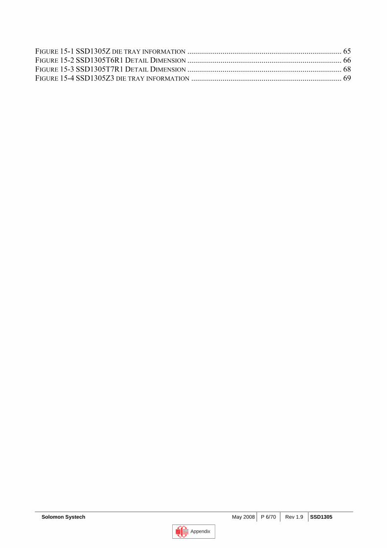
FIGURE 15-1 SSD1305Z DIE TRAY INFORMATION ............................................................................... 65 FIGURE 15-2 SSD1305T6R1 DETAIL DIMENSION ............................................................................... 66 FIGURE 15-3 SSD1305T7R1 DETAIL DIMENSION ............................................................................... 68 FIGURE 15-4 SSD1305Z3 DIE TRAY INFORMATION ............................................................................. 69
Appendix
SSD1305 Rev 1.9 P 7/70 May 2008 Solomon Systech
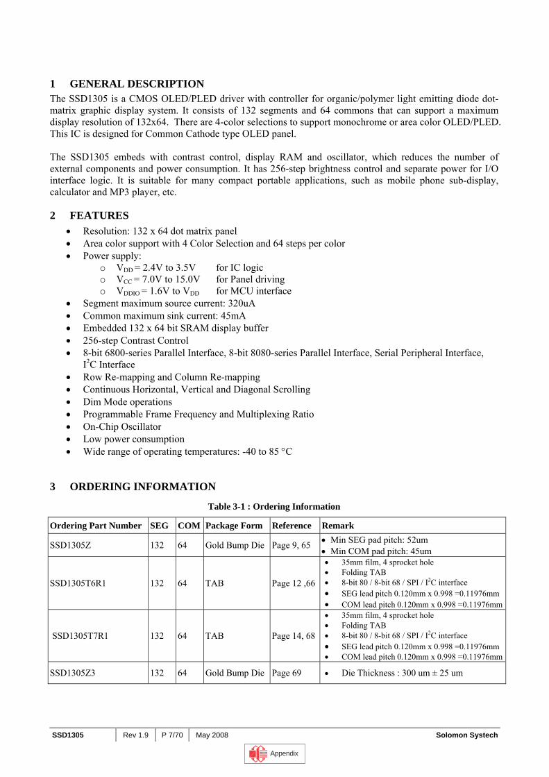
1 GENERAL DESCRIPTION The SSD1305 is a CMOS OLED/PLED driver with controller for organic/polymer light emitting diode dot-matrix graphic display system. It consists of 132 segments and 64 commons that can support a maximum display resolution of 132x64. There are 4-color selections to support monochrome or area color OLED/PLED. This IC is designed for Common Cathode type OLED panel. The SSD1305 embeds with contrast control, display RAM and oscillator, which reduces the number of external components and power consumption. It has 256-step brightness control and separate power for I/O interface logic. It is suitable for many compact portable applications, such as mobile phone sub-display, calculator and MP3 player, etc.
2 FEATURES • Resolution: 132 x 64 dot matrix panel • Area color support with 4 Color Selection and 64 steps per color • Power supply:
o VDD = 2.4V to 3.5V for IC logic o VCC = 7.0V to 15.0V for Panel driving o VDDIO = 1.6V to VDD for MCU interface
• Segment maximum source current: 320uA • Common maximum sink current: 45mA • Embedded 132 x 64 bit SRAM display buffer • 256-step Contrast Control • 8-bit 6800-series Parallel Interface, 8-bit 8080-series Parallel Interface, Serial Peripheral Interface,
I2C Interface • Row Re-mapping and Column Re-mapping • Continuous Horizontal, Vertical and Diagonal Scrolling • Dim Mode operations • Programmable Frame Frequency and Multiplexing Ratio • On-Chip Oscillator • Low power consumption • Wide range of operating temperatures: -40 to 85 °C
3 ORDERING INFORMATION
Table 3-1 : Ordering Information
Ordering Part Number SEG COM Package Form Reference Remark
SSD1305Z 132 64 Gold Bump Die Page 9, 65 • Min SEG pad pitch: 52um • Min COM pad pitch: 45um
SSD1305T6R1 132 64 TAB Page 12 ,66
• 35mm film, 4 sprocket hole • Folding TAB • 8-bit 80 / 8-bit 68 / SPI / I2C interface • SEG lead pitch 0.120mm x 0.998 =0.11976mm• COM lead pitch 0.120mm x 0.998 =0.11976mm
SSD1305T7R1 132 64 TAB Page 14, 68
• 35mm film, 4 sprocket hole • Folding TAB • 8-bit 80 / 8-bit 68 / SPI / I2C interface • SEG lead pitch 0.120mm x 0.998 =0.11976mm• COM lead pitch 0.120mm x 0.998 =0.11976mm
SSD1305Z3 132 64 Gold Bump Die Page 69 • Die Thickness : 300 um ± 25 um
Appendix
Solomon Systech May 2008 P 8/70 Rev 1.9 SSD1305
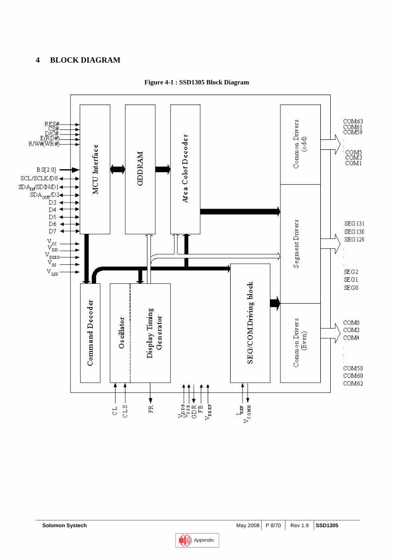
4 BLOCK DIAGRAM
Figure 4-1 : SSD1305 Block Diagram
Appendix
SSD1305 Rev 1.9 P 9/70 May 2008 Solomon Systech
5 DIE PAD FLOOR PLAN
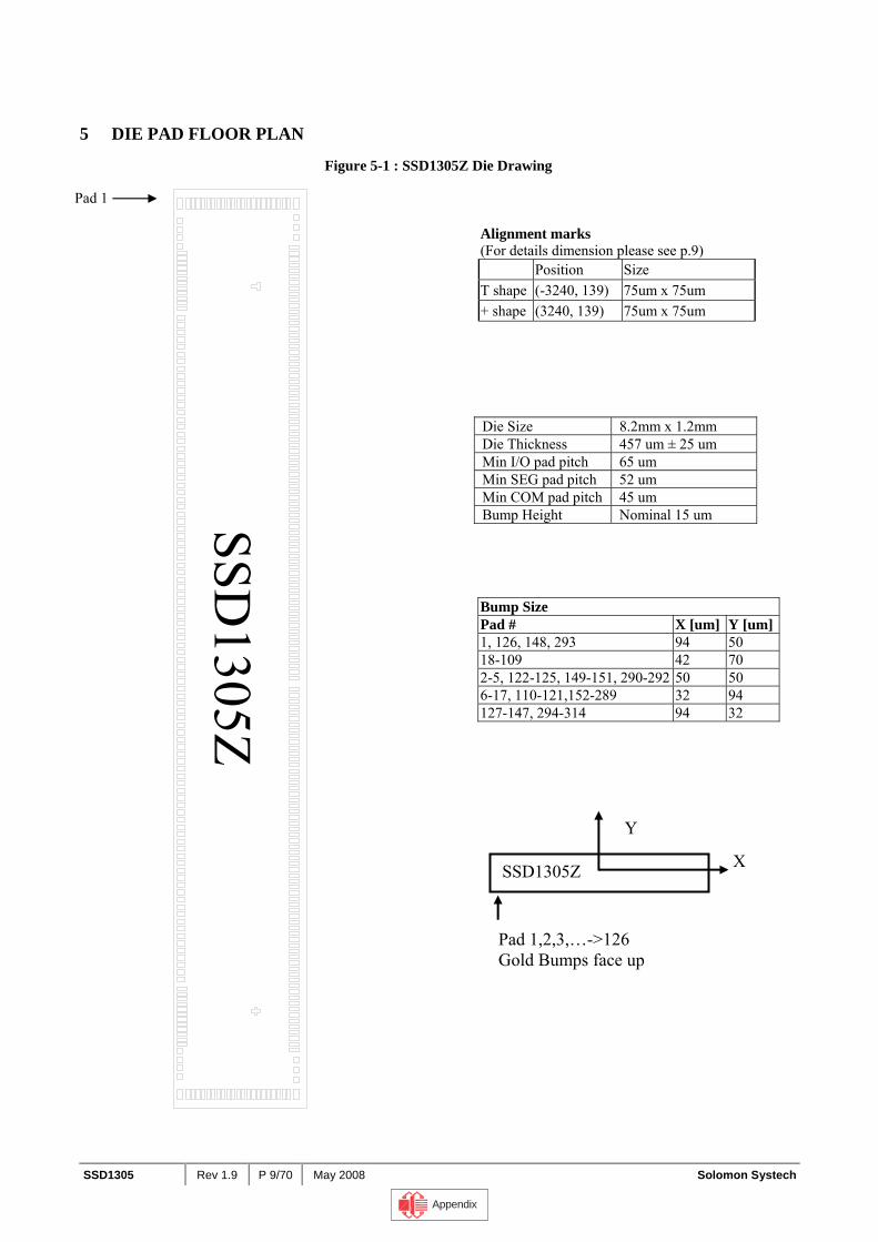
Figure 5-1 : SSD1305Z Die Drawing
Pad 1
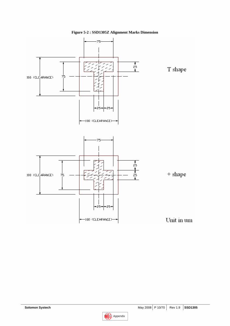
Alignment marks (For details dimension please see p.9) Position Size T shape (-3240, 139) 75um x 75um + shape (3240, 139) 75um x 75um
Die Size 8.2mm x 1.2mm Die Thickness 457 um ± 25 um Min I/O pad pitch 65 um Min SEG pad pitch 52 um Min COM pad pitch 45 um Bump Height Nominal 15 um
Bump Size Pad # X [um] Y [um]1, 126, 148, 293 94 50 18-109 42 70 2-5, 122-125, 149-151, 290-292 50 50 6-17, 110-121,152-289 32 94 127-147, 294-314 94 32
Pad 1,2,3,…->126 Gold Bumps face up
SSD1305Z X
Y
SSD1305Z
Appendix
Solomon Systech May 2008 P 10/70 Rev 1.9 SSD1305
Figure 5-2 : SSD1305Z Alignment Marks Dimension
Appendix
SSD1305 Rev 1.9 P 11/70 May 2008 Solomon Systech
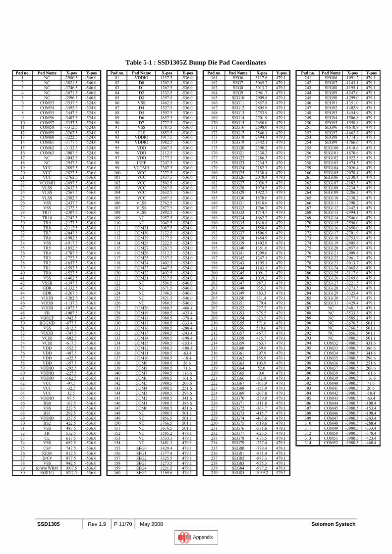
Table 5-1 : SSD1305Z Bump Die Pad Coordinates Pad no. Pad Name X-pos Y-pos Pad no. Pad Name X-pos Y-pos Pad no. Pad Name X-pos Y-pos Pad no. Pad Name X-pos Y-pos
1 NC -3980.5 -546.0 81 VDDIO 1137.5 -536.0 161 SEG6 3117.6 479.1 241 SEG86 -1091.2 479.12 NC -3821.5 -546.0 82 D0 1202.5 -536.0 162 SEG7 3065.7 479.1 242 SEG87 -1143.1 479.13 NC -3746.5 -546.0 83 D1 1267.5 -536.0 163 SEG8 3013.7 479.1 243 SEG88 -1195.1 479.14 NC -3671.5 -546.0 84 D2 1332.5 -536.0 164 SEG9 2961.7 479.1 244 SEG89 -1247.0 479.15 NC -3596.5 -546.0 85 D3 1397.5 -536.0 165 SEG10 2909.8 479.1 245 SEG90 -1299.0 479.16 COM53 -3537.5 -524.0 86 VSS 1462.5 -536.0 166 SEG11 2857.8 479.1 246 SEG91 -1351.0 479.17 COM54 -3492.5 -524.0 87 D4 1527.5 -536.0 167 SEG12 2805.9 479.1 247 SEG92 -1402.9 479.18 COM55 -3447.5 -524.0 88 D5 1592.5 -536.0 168 SEG13 2753.9 479.1 248 SEG93 -1454.9 479.19 COM56 -3402.5 -524.0 89 D6 1657.5 -536.0 169 SEG14 2701.9 479.1 249 SEG94 -1506.8 479.1
10 COM57 -3357.5 -524.0 90 D7 1722.5 -536.0 170 SEG15 2650.0 479.1 250 SEG95 -1558.8 479.111 COM58 -3312.5 -524.0 91 VSS 1787.5 -536.0 171 SEG16 2598.0 479.1 251 SEG96 -1610.8 479.112 COM59 -3267.5 -524.0 92 CLS 1852.5 -536.0 172 SEG17 2546.1 479.1 252 SEG97 -1662.7 479.113 COM60 -3222.5 -524.0 93 VDDIO 1917.5 -536.0 173 SEG18 2494.1 479.1 253 SEG98 -1714.7 479.114 COM61 -3177.5 -524.0 94 VDDIO 1982.5 -536.0 174 SEG19 2442.1 479.1 254 SEG99 -1766.6 479.115 COM62 -3132.5 -524.0 95 VDD 2047.5 -536.0 175 SEG20 2390.2 479.1 255 SEG100 -1818.6 479.116 COM63 -3087.5 -524.0 96 VDD 2112.5 -536.0 176 SEG21 2338.2 479.1 256 SEG101 -1870.6 479.117 NC -3042.5 -524.0 97 VDD 2177.5 -536.0 177 SEG22 2286.3 479.1 257 SEG102 -1922.5 479.118 NC -2957.5 -536.0 98 IREF 2242.5 -536.0 178 SEG23 2234.3 479.1 258 SEG103 -1974.5 479.119 VCC -2892.5 -536.0 99 VCOMH 2307.5 -536.0 179 SEG24 2182.3 479.1 259 SEG104 -2026.4 479.120 VCC -2827.5 -536.0 100 VCC 2372.5 -536.0 180 SEG25 2130.4 479.1 260 SEG105 -2078.4 479.121 VCC -2762.5 -536.0 101 VCC 2437.5 -536.0 181 SEG26 2078.4 479.1 261 SEG106 -2130.4 479.122 VCOMH -2697.5 -536.0 102 VCC 2502.5 -536.0 182 SEG27 2026.5 479.1 262 SEG107 -2182.3 479.123 VLSS -2632.5 -536.0 103 VCC 2567.5 -536.0 183 SEG28 1974.5 479.1 263 SEG108 -2234.3 479.124 VLSS -2567.5 -536.0 104 VCC 2632.5 -536.0 184 SEG29 1922.5 479.1 264 SEG109 -2286.2 479.125 VLSS -2502.5 -536.0 105 VCC 2697.5 -536.0 185 SEG30 1870.6 479.1 265 SEG110 -2338.2 479.126 VSS -2437.5 -536.0 106 VLSS 2762.5 -536.0 186 SEG31 1818.6 479.1 266 SEG111 -2390.2 479.127 VSS -2372.5 -536.0 107 VLSS 2827.5 -536.0 187 SEG32 1766.7 479.1 267 SEG112 -2442.1 479.128 TR11 -2307.5 -536.0 108 VLSS 2892.5 -536.0 188 SEG33 1714.7 479.1 268 SEG113 -2494.1 479.129 TR10 -2242.5 -536.0 109 NC 2957.5 -536.0 189 SEG34 1662.7 479.1 269 SEG114 -2546.0 479.130 TR9 -2177.5 -536.0 110 NC 3042.5 -524.0 190 SEG35 1610.8 479.1 270 SEG115 -2598.0 479.131 TR8 -2112.5 -536.0 111 COM31 3087.5 -524.0 191 SEG36 1558.8 479.1 271 SEG116 -2650.0 479.132 TR7 -2047.5 -536.0 112 COM30 3132.5 -524.0 192 SEG37 1506.9 479.1 272 SEG117 -2701.9 479.133 TR6 -1982.5 -536.0 113 COM29 3177.5 -524.0 193 SEG38 1454.9 479.1 273 SEG118 -2753.9 479.134 VSS -1917.5 -536.0 114 COM28 3222.5 -524.0 194 SEG39 1402.9 479.1 274 SEG119 -2805.8 479.135 TR5 -1852.5 -536.0 115 COM27 3267.5 -524.0 195 SEG40 1351.0 479.1 275 SEG120 -2857.8 479.136 TR4 -1787.5 -536.0 116 COM26 3312.5 -524.0 196 SEG41 1299.0 479.1 276 SEG121 -2909.8 479.137 TR3 -1722.5 -536.0 117 COM25 3357.5 -524.0 197 SEG42 1247.1 479.1 277 SEG122 -2961.7 479.138 TR2 -1657.5 -536.0 118 COM24 3402.5 -524.0 198 SEG43 1195.1 479.1 278 SEG123 -3013.7 479.139 TR1 -1592.5 -536.0 119 COM23 3447.5 -524.0 199 SEG44 1143.1 479.1 279 SEG124 -3065.6 479.140 TR0 -1527.5 -536.0 120 COM22 3492.5 -524.0 200 SEG45 1091.2 479.1 280 SEG125 -3117.6 479.141 VSS -1462.5 -536.0 121 COM21 3537.5 -524.0 201 SEG46 1039.2 479.1 281 SEG126 -3169.6 479.142 VSSB -1397.5 -536.0 122 NC 3596.5 -546.0 202 SEG47 987.3 479.1 282 SEG127 -3221.5 479.143 GDR -1332.5 -536.0 123 NC 3671.5 -546.0 203 SEG48 935.3 479.1 283 SEG128 -3273.5 479.144 GDR -1267.5 -536.0 124 NC 3746.5 -546.0 204 SEG49 883.3 479.1 284 SEG129 -3325.4 479.145 VDDB -1202.5 -536.0 125 NC 3821.5 -546.0 205 SEG50 831.4 479.1 285 SEG130 -3377.4 479.146 VDDB -1137.5 -536.0 126 NC 3980.5 -546.0 206 SEG51 779.4 479.1 286 SEG131 -3429.4 479.147 VDDB -1072.5 -536.0 127 COM20 3980.5 -468.4 207 SEG52 727.5 479.1 287 NC -3481.3 479.148 FB -1007.5 -536.0 128 COM19 3980.5 -423.4 208 SEG53 675.5 479.1 288 NC -3533.3 479.149 VBREF -942.5 -536.0 129 COM18 3980.5 -378.4 209 SEG54 623.5 479.1 289 NC -3585.2 479.150 BGGND -877.5 -536.0 130 COM17 3980.5 -333.4 210 SEG55 571.6 479.1 290 NC -3676.5 501.151 VSS -812.5 -536.0 131 COM16 3980.5 -288.4 211 SEG56 519.6 479.1 291 NC -3766.5 501.152 VDDB -747.5 -536.0 132 COM15 3980.5 -243.4 212 SEG57 467.7 479.1 292 NC -3856.5 501.153 VCIR -682.5 -536.0 133 COM14 3980.5 -198.4 213 SEG58 415.7 479.1 293 NC -3980.5 501.154 VCIR -617.5 -536.0 134 COM13 3980.5 -153.4 214 SEG59 363.7 479.1 294 COM32 -3980.5 431.655 VDD -552.5 -536.0 135 COM12 3980.5 -108.4 215 SEG60 259.8 479.1 295 COM33 -3980.5 386.656 VDD -487.5 -536.0 136 COM11 3980.5 -63.4 216 SEG61 207.9 479.1 296 COM34 -3980.5 341.657 VDD -422.5 -536.0 137 COM10 3980.5 -18.4 217 SEG62 155.9 479.1 297 COM35 -3980.5 296.658 VDD -357.5 -536.0 138 COM9 3980.5 26.6 218 SEG63 103.9 479.1 298 COM36 -3980.5 251.659 VDDIO -292.5 -536.0 139 COM8 3980.5 71.6 219 SEG64 52.0 479.1 299 COM37 -3980.5 206.660 VDDIO -227.5 -536.0 140 COM7 3980.5 116.6 220 SEG65 0.0 479.1 300 COM38 -3980.5 161.661 VDDIO -162.5 -536.0 141 COM6 3980.5 161.6 221 SEG66 -52.0 479.1 301 COM39 -3980.5 116.662 VCC -97.5 -536.0 142 COM5 3980.5 206.6 222 SEG67 -103.9 479.1 302 COM40 -3980.5 71.663 VCC -32.5 -536.0 143 COM4 3980.5 251.6 223 SEG68 -155.9 479.1 303 COM41 -3980.5 26.664 VCC 32.5 -536.0 144 COM3 3980.5 296.6 224 SEG69 -207.8 479.1 304 COM42 -3980.5 -18.465 VDDIO 97.5 -536.0 145 COM2 3980.5 341.6 225 SEG70 -259.8 479.1 305 COM43 -3980.5 -63.466 BS0 162.5 -536.0 146 COM1 3980.5 386.6 226 SEG71 -311.8 479.1 306 COM44 -3980.5 -108.467 VSS 227.5 -536.0 147 COM0 3980.5 431.6 227 SEG72 -363.7 479.1 307 COM45 -3980.5 -153.468 BS1 292.5 -536.0 148 NC 3980.5 501.1 228 SEG73 -415.7 479.1 308 COM46 -3980.5 -198.469 VDDIO 357.5 -536.0 149 NC 3856.5 501.1 229 SEG74 -467.6 479.1 309 COM47 -3980.5 -243.470 BS2 422.5 -536.0 150 NC 3766.5 501.1 230 SEG75 -519.6 479.1 310 COM48 -3980.5 -288.471 VSS 487.5 -536.0 151 NC 3676.5 501.1 231 SEG76 -571.6 479.1 311 COM49 -3980.5 -333.472 FR 552.5 -536.0 152 NC 3585.2 479.1 232 SEG77 -623.5 479.1 312 COM50 -3980.5 -378.473 CL 617.5 -536.0 153 NC 3533.3 479.1 233 SEG78 -675.5 479.1 313 COM51 -3980.5 -423.474 VSS 682.5 -536.0 154 NC 3481.3 479.1 234 SEG79 -727.4 479.1 314 COM52 -3980.5 -468.475 CS# 747.5 -536.0 155 SEG0 3429.4 479.1 235 SEG80 -779.4 479.176 RES# 812.5 -536.0 156 SEG1 3377.4 479.1 236 SEG81 -831.4 479.177 D/C# 877.5 -536.0 157 SEG2 3325.5 479.1 237 SEG82 -883.3 479.178 VSS 942.5 -536.0 158 SEG3 3273.5 479.1 238 SEG83 -935.3 479.179 R/W#(WR#) 1007.5 -536.0 159 SEG4 3221.5 479.1 239 SEG84 -987.2 479.180 E(RD#) 1072.5 -536.0 160 SEG5 3169.6 479.1 240 SEG85 -1039.2 479.1
Appendix
Solomon Systech May 2008 P 12/70 Rev 1.9 SSD1305
6 PIN ARRANGEMENT
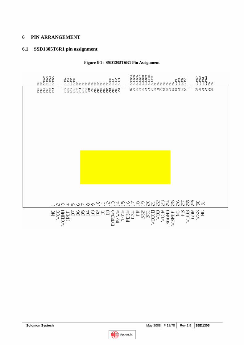
6.1 SSD1305T6R1 pin assignment
Figure 6-1 : SSD1305T6R1 Pin Assignment
Appendix
SSD1305 Rev 1.9 P 13/70 May 2008 Solomon Systech
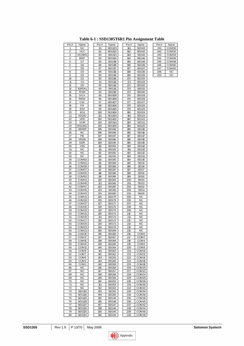
Table 6-1 : SSD1305T6R1 Pin Assignment Table
Pin # Name Pin # Name Pin # Name Pin # Name1 NC 81 SEG123 161 SEG43 241 COM502 VCC 82 SEG122 162 SEG42 242 COM523 VCOMH 83 SEG121 163 SEG41 243 COM544 IREF 84 SEG120 164 SEG40 244 COM565 D7 85 SEG119 165 SEG39 245 COM586 D6 86 SEG118 166 SEG38 246 COM607 D5 87 SEG117 167 SEG37 247 COM628 D4 88 SEG116 168 SEG36 248 NC9 D3 89 SEG115 169 SEG35 249 NC10 D2 90 SEG114 170 SEG3411 D1 91 SEG113 171 SEG3312 D0 92 SEG112 172 SEG3213 E(RD#) 93 SEG111 173 SEG3114 R/W# 94 SEG110 174 SEG3015 D/C# 95 SEG109 175 SEG2916 RES# 96 SEG108 176 SEG2817 CS# 97 SEG107 177 SEG2718 FR 98 SEG106 178 SEG2619 BS2 99 SEG105 179 SEG2520 BS1 100 SEG104 180 SEG2421 VDDIO 101 SEG103 181 SEG2322 VDD 102 SEG102 182 SEG2223 VCIR 103 SEG101 183 SEG2124 BGGND 104 SEG100 184 SEG2025 VBREF 105 SEG99 185 SEG1926 NC 106 SEG98 186 SEG1827 FB 107 SEG97 187 SEG1728 VDDB 108 SEG96 188 SEG1629 GDR 109 SEG95 189 SEG1530 VSS 110 SEG94 190 SEG1431 NC 111 SEG93 191 SEG1332 NC 112 SEG92 192 SEG1233 NC 113 SEG91 193 SEG1134 COM63 114 SEG90 194 SEG1035 COM61 115 SEG89 195 SEG936 COM59 116 SEG88 196 SEG837 COM57 117 SEG87 197 SEG738 COM55 118 SEG86 198 SEG639 COM53 119 SEG85 199 SEG540 COM51 120 SEG84 200 SEG441 COM49 121 SEG83 201 SEG342 COM47 122 SEG82 202 SEG243 COM45 123 SEG81 203 SEG144 COM43 124 SEG80 204 SEG045 COM41 125 SEG79 205 NC46 COM39 126 SEG78 206 NC47 COM37 127 SEG77 207 NC48 COM35 128 SEG76 208 NC49 COM33 129 SEG75 209 NC50 COM31 130 SEG74 210 NC51 COM29 131 SEG73 211 NC52 COM27 132 SEG72 212 NC53 COM25 133 SEG71 213 NC54 COM23 134 SEG70 214 NC55 COM21 135 SEG69 215 NC56 COM19 136 SEG68 216 COM057 COM17 137 SEG67 217 COM258 COM15 138 SEG66 218 COM459 COM13 139 SEG65 219 COM660 COM11 140 SEG64 220 COM861 COM9 141 SEG63 221 COM1062 COM7 142 SEG62 222 COM1263 COM5 143 SEG61 223 COM1464 COM3 144 SEG60 224 COM1665 COM1 145 SEG59 225 COM1866 NC 146 SEG58 226 COM2067 NC 147 SEG57 227 COM2268 NC 148 SEG56 228 COM2469 NC 149 SEG55 229 COM2670 NC 150 SEG54 230 COM2871 NC 151 SEG53 231 COM3072 NC 152 SEG52 232 COM3273 SEG131 153 SEG51 233 COM3474 SEG130 154 SEG50 234 COM3675 SEG129 155 SEG49 235 COM3876 SEG128 156 SEG48 236 COM4077 SEG127 157 SEG47 237 COM4278 SEG126 158 SEG46 238 COM4479 SEG125 159 SEG45 239 COM4680 SEG124 160 SEG44 240 COM48
Appendix
Solomon Systech May 2008 P 14/70 Rev 1.9 SSD1305
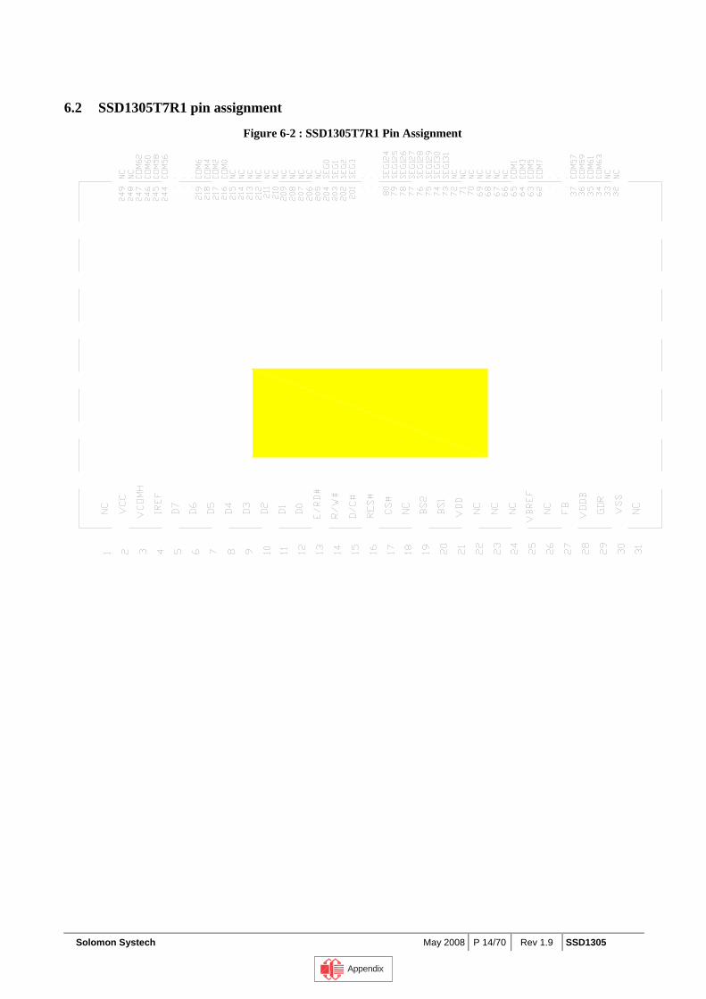
6.2 SSD1305T7R1 pin assignment
Figure 6-2 : SSD1305T7R1 Pin Assignment
Appendix
SSD1305 Rev 1.9 P 15/70 May 2008 Solomon Systech
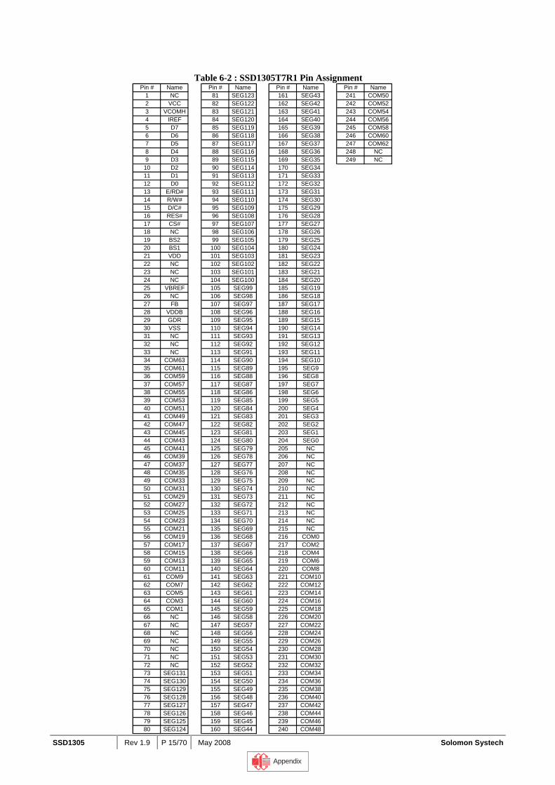
Table 6-2 : SSD1305T7R1 Pin Assignment Pin # Name Pin # Name Pin # Name Pin # Name
1 NC 81 SEG123 161 SEG43 241 COM502 VCC 82 SEG122 162 SEG42 242 COM523 VCOMH 83 SEG121 163 SEG41 243 COM544 IREF 84 SEG120 164 SEG40 244 COM565 D7 85 SEG119 165 SEG39 245 COM586 D6 86 SEG118 166 SEG38 246 COM607 D5 87 SEG117 167 SEG37 247 COM628 D4 88 SEG116 168 SEG36 248 NC9 D3 89 SEG115 169 SEG35 249 NC
10 D2 90 SEG114 170 SEG3411 D1 91 SEG113 171 SEG3312 D0 92 SEG112 172 SEG3213 E/RD# 93 SEG111 173 SEG3114 R/W# 94 SEG110 174 SEG3015 D/C# 95 SEG109 175 SEG2916 RES# 96 SEG108 176 SEG2817 CS# 97 SEG107 177 SEG2718 NC 98 SEG106 178 SEG2619 BS2 99 SEG105 179 SEG2520 BS1 100 SEG104 180 SEG2421 VDD 101 SEG103 181 SEG2322 NC 102 SEG102 182 SEG2223 NC 103 SEG101 183 SEG2124 NC 104 SEG100 184 SEG2025 VBREF 105 SEG99 185 SEG1926 NC 106 SEG98 186 SEG1827 FB 107 SEG97 187 SEG1728 VDDB 108 SEG96 188 SEG1629 GDR 109 SEG95 189 SEG1530 VSS 110 SEG94 190 SEG1431 NC 111 SEG93 191 SEG1332 NC 112 SEG92 192 SEG1233 NC 113 SEG91 193 SEG1134 COM63 114 SEG90 194 SEG1035 COM61 115 SEG89 195 SEG936 COM59 116 SEG88 196 SEG837 COM57 117 SEG87 197 SEG738 COM55 118 SEG86 198 SEG639 COM53 119 SEG85 199 SEG540 COM51 120 SEG84 200 SEG441 COM49 121 SEG83 201 SEG342 COM47 122 SEG82 202 SEG243 COM45 123 SEG81 203 SEG144 COM43 124 SEG80 204 SEG045 COM41 125 SEG79 205 NC46 COM39 126 SEG78 206 NC47 COM37 127 SEG77 207 NC48 COM35 128 SEG76 208 NC49 COM33 129 SEG75 209 NC50 COM31 130 SEG74 210 NC51 COM29 131 SEG73 211 NC52 COM27 132 SEG72 212 NC53 COM25 133 SEG71 213 NC54 COM23 134 SEG70 214 NC55 COM21 135 SEG69 215 NC56 COM19 136 SEG68 216 COM057 COM17 137 SEG67 217 COM258 COM15 138 SEG66 218 COM459 COM13 139 SEG65 219 COM660 COM11 140 SEG64 220 COM861 COM9 141 SEG63 221 COM1062 COM7 142 SEG62 222 COM1263 COM5 143 SEG61 223 COM1464 COM3 144 SEG60 224 COM1665 COM1 145 SEG59 225 COM1866 NC 146 SEG58 226 COM2067 NC 147 SEG57 227 COM2268 NC 148 SEG56 228 COM2469 NC 149 SEG55 229 COM2670 NC 150 SEG54 230 COM2871 NC 151 SEG53 231 COM3072 NC 152 SEG52 232 COM3273 SEG131 153 SEG51 233 COM3474 SEG130 154 SEG50 234 COM3675 SEG129 155 SEG49 235 COM3876 SEG128 156 SEG48 236 COM4077 SEG127 157 SEG47 237 COM4278 SEG126 158 SEG46 238 COM4479 SEG125 159 SEG45 239 COM4680 SEG124 160 SEG44 240 COM48
Appendix
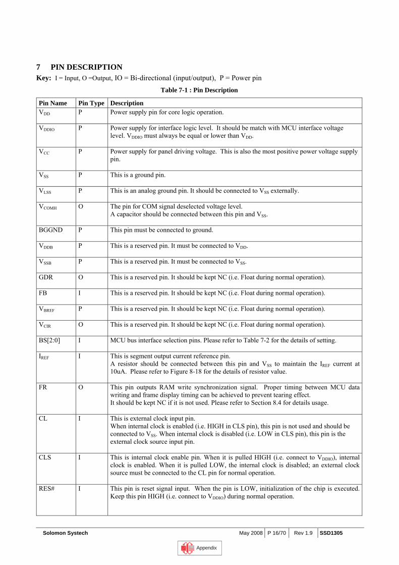
Solomon Systech May 2008 P 16/70 Rev 1.9 SSD1305
7 PIN DESCRIPTION Key: I = Input, O =Output, IO = Bi-directional (input/output), P = Power pin
Table 7-1 : Pin Description
Pin Name Pin Type Description VDD P Power supply pin for core logic operation.
VDDIO P Power supply for interface logic level. It should be match with MCU interface voltage
level. VDDIO must always be equal or lower than VDD.
VCC P Power supply for panel driving voltage. This is also the most positive power voltage supply pin.
VSS P This is a ground pin.
VLSS P This is an analog ground pin. It should be connected to VSS externally.
VCOMH O The pin for COM signal deselected voltage level. A capacitor should be connected between this pin and VSS.
BGGND P This pin must be connected to ground.
VDDB P This is a reserved pin. It must be connected to VDD.
VSSB P This is a reserved pin. It must be connected to VSS.
GDR O This is a reserved pin. It should be kept NC (i.e. Float during normal operation).
FB I This is a reserved pin. It should be kept NC (i.e. Float during normal operation).
VBREF P This is a reserved pin. It should be kept NC (i.e. Float during normal operation).
VCIR O This is a reserved pin. It should be kept NC (i.e. Float during normal operation).
BS[2:0]
I MCU bus interface selection pins. Please refer to Table 7-2 for the details of setting.
IREF
I This is segment output current reference pin. A resistor should be connected between this pin and VSS to maintain the IREF current at 10uA. Please refer to Figure 8-18 for the details of resistor value.
FR O This pin outputs RAM write synchronization signal. Proper timing between MCU data writing and frame display timing can be achieved to prevent tearing effect. It should be kept NC if it is not used. Please refer to Section 8.4 for details usage.
CL I This is external clock input pin. When internal clock is enabled (i.e. HIGH in CLS pin), this pin is not used and should be connected to VSS. When internal clock is disabled (i.e. LOW in CLS pin), this pin is the external clock source input pin.
CLS I This is internal clock enable pin. When it is pulled HIGH (i.e. connect to VDDIO), internal clock is enabled. When it is pulled LOW, the internal clock is disabled; an external clock source must be connected to the CL pin for normal operation.
RES# I This pin is reset signal input. When the pin is LOW, initialization of the chip is executed. Keep this pin HIGH (i.e. connect to VDDIO) during normal operation.
Appendix
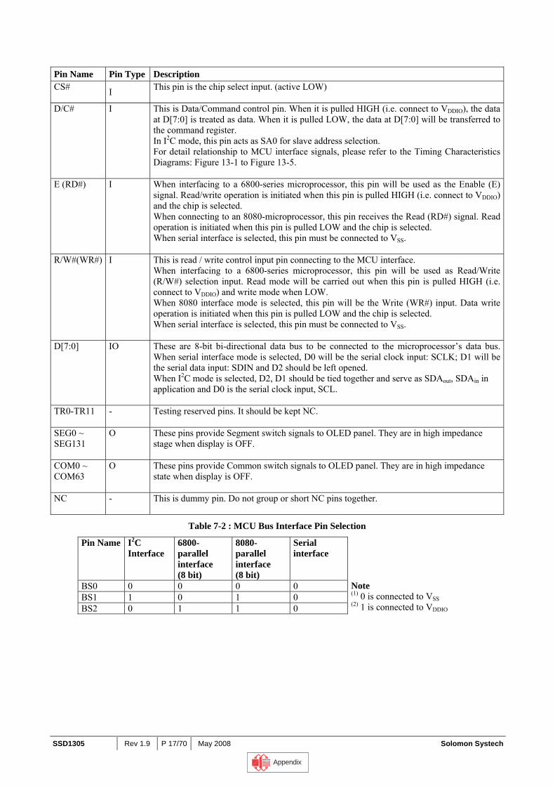
SSD1305 Rev 1.9 P 17/70 May 2008 Solomon Systech
Pin Name Pin Type Description CS# I This pin is the chip select input. (active LOW)
D/C# I This is Data/Command control pin. When it is pulled HIGH (i.e. connect to VDDIO), the data
at D[7:0] is treated as data. When it is pulled LOW, the data at D[7:0] will be transferred to the command register. In I2C mode, this pin acts as SA0 for slave address selection. For detail relationship to MCU interface signals, please refer to the Timing Characteristics Diagrams: Figure 13-1 to Figure 13-5.
E (RD#) I When interfacing to a 6800-series microprocessor, this pin will be used as the Enable (E) signal. Read/write operation is initiated when this pin is pulled HIGH (i.e. connect to VDDIO) and the chip is selected. When connecting to an 8080-microprocessor, this pin receives the Read (RD#) signal. Read operation is initiated when this pin is pulled LOW and the chip is selected. When serial interface is selected, this pin must be connected to VSS.
R/W#(WR#) I This is read / write control input pin connecting to the MCU interface. When interfacing to a 6800-series microprocessor, this pin will be used as Read/Write (R/W#) selection input. Read mode will be carried out when this pin is pulled HIGH (i.e. connect to VDDIO) and write mode when LOW. When 8080 interface mode is selected, this pin will be the Write (WR#) input. Data write operation is initiated when this pin is pulled LOW and the chip is selected. When serial interface is selected, this pin must be connected to VSS.
D[7:0] IO These are 8-bit bi-directional data bus to be connected to the microprocessor’s data bus. When serial interface mode is selected, D0 will be the serial clock input: SCLK; D1 will be the serial data input: SDIN and D2 should be left opened. When I2C mode is selected, D2, D1 should be tied together and serve as SDAout, SDAin in application and D0 is the serial clock input, SCL.
TR0-TR11 - Testing reserved pins. It should be kept NC.
SEG0 ~ SEG131
O These pins provide Segment switch signals to OLED panel. They are in high impedance stage when display is OFF.
COM0 ~ COM63
O These pins provide Common switch signals to OLED panel. They are in high impedance state when display is OFF.
NC - This is dummy pin. Do not group or short NC pins together.
Table 7-2 : MCU Bus Interface Pin Selection
Pin Name I2C Interface
6800-parallel interface (8 bit)
8080-parallel interface (8 bit)
Serial interface
BS0 0 0 0 0 BS1 1 0 1 0 BS2 0 1 1 0
Note (1) 0 is connected to VSS (2) 1 is connected to VDDIO
Appendix
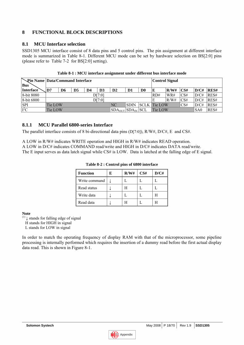
Solomon Systech May 2008 P 18/70 Rev 1.9 SSD1305
8 FUNCTIONAL BLOCK DESCRIPTIONS
8.1 MCU Interface selection SSD1305 MCU interface consist of 8 data pins and 5 control pins. The pin assignment at different interface mode is summarized in Table 8-1. Different MCU mode can be set by hardware selection on BS[2:0] pins (please refer to Table 7-2 for BS[2:0] setting).
Table 8-1 : MCU interface assignment under different bus interface mode
Data/Command Interface Control Signal Pin Name Bus Interface D7 D6 D5 D4 D3 D2 D1 D0 E R/W# CS# D/C# RES# 8-bit 8080 D[7:0] RD# WR# CS# D/C# RES# 8-bit 6800 D[7:0] E R/W# CS# D/C# RES# SPI Tie LOW NC SDIN SCLK Tie LOW CS# D/C# RES# I2C Tie LOW SDAOUT SDAIN SCL Tie LOW SA0 RES#
8.1.1 MCU Parallel 6800-series Interface The parallel interface consists of 8 bi-directional data pins (D[7:0]), R/W#, D/C#, E and CS#. A LOW in R/W# indicates WRITE operation and HIGH in R/W# indicates READ operation. A LOW in D/C# indicates COMMAND read/write and HIGH in D/C# indicates DATA read/write. The E input serves as data latch signal while CS# is LOW. Data is latched at the falling edge of E signal.
Table 8-2 : Control pins of 6800 interface
Function E R/W# CS# D/C#
Write command ↓ L L L
Read status ↓ H L L
Write data ↓ L L H
Read data ↓ H L H Note (1) ↓ stands for falling edge of signal H stands for HIGH in signal L stands for LOW in signal In order to match the operating frequency of display RAM with that of the microprocessor, some pipeline processing is internally performed which requires the insertion of a dummy read before the first actual display data read. This is shown in Figure 8-1.
Appendix
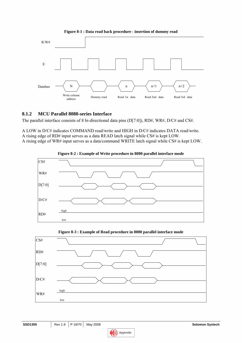
SSD1305 Rev 1.9 P 19/70 May 2008 Solomon Systech
Figure 8-1 : Data read back procedure - insertion of dummy read
N n n+1 n+2
R/W#
E
Databus
Write columnaddress Read 1st dataDummy read Read 2nd data Read 3rd data
8.1.2 MCU Parallel 8080-series Interface The parallel interface consists of 8 bi-directional data pins (D[7:0]), RD#, WR#, D/C# and CS#. A LOW in D/C# indicates COMMAND read/write and HIGH in D/C# indicates DATA read/write. A rising edge of RD# input serves as a data READ latch signal while CS# is kept LOW. A rising edge of WR# input serves as a data/command WRITE latch signal while CS# is kept LOW.
Figure 8-2 : Example of Write procedure in 8080 parallel interface mode
CS#
WR#
D[7:0]
D/C#
RD#high
low
Figure 8-3 : Example of Read procedure in 8080 parallel interface mode
CS#
WR#
D[7:0]
D/C#
RD#
high
low
Appendix
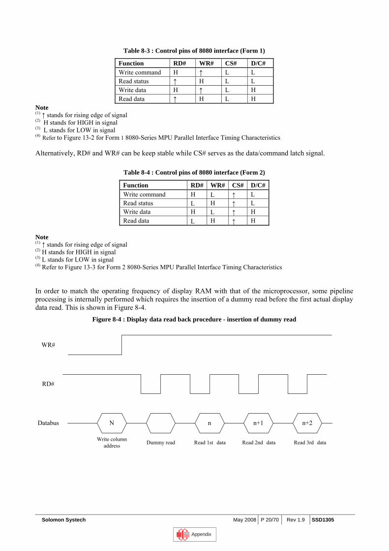
Solomon Systech May 2008 P 20/70 Rev 1.9 SSD1305
Table 8-3 : Control pins of 8080 interface (Form 1)
Function RD# WR# CS# D/C# Write command H ↑ L L Read status ↑ H L L Write data H ↑ L H Read data ↑ H L H
Note (1) ↑ stands for rising edge of signal (2) H stands for HIGH in signal (3) L stands for LOW in signal (4) Refer to Figure 13-2 for Form 1 8080-Series MPU Parallel Interface Timing Characteristics Alternatively, RD# and WR# can be keep stable while CS# serves as the data/command latch signal.
Table 8-4 : Control pins of 8080 interface (Form 2)
Function RD# WR# CS# D/C#Write command H L ↑ L Read status L H ↑ L Write data H L ↑ H Read data L H ↑ H
Note (1) ↑ stands for rising edge of signal (2) H stands for HIGH in signal (3) L stands for LOW in signal (4) Refer to Figure 13-3 for Form 2 8080-Series MPU Parallel Interface Timing Characteristics In order to match the operating frequency of display RAM with that of the microprocessor, some pipeline processing is internally performed which requires the insertion of a dummy read before the first actual display data read. This is shown in Figure 8-4.
Figure 8-4 : Display data read back procedure - insertion of dummy read
N n n+1 n+2
WR#
RD#
Databus
Write columnaddress Read 1st dataDummy read Read 2nd data Read 3rd data
Appendix
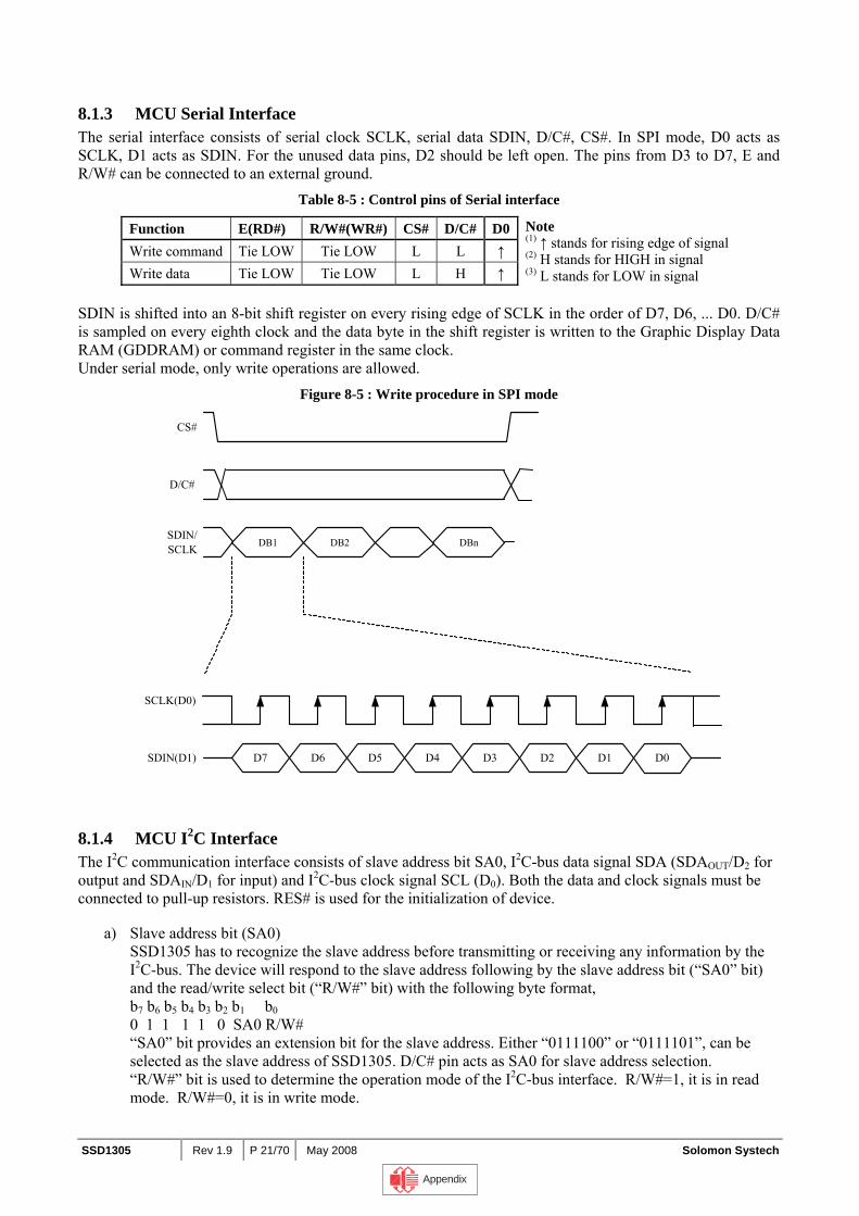
SSD1305 Rev 1.9 P 21/70 May 2008 Solomon Systech
8.1.3 MCU Serial Interface The serial interface consists of serial clock SCLK, serial data SDIN, D/C#, CS#. In SPI mode, D0 acts as SCLK, D1 acts as SDIN. For the unused data pins, D2 should be left open. The pins from D3 to D7, E and R/W# can be connected to an external ground.
Table 8-5 : Control pins of Serial interface
Function E(RD#) R/W#(WR#) CS# D/C# D0Write command Tie LOW Tie LOW L L ↑Write data Tie LOW Tie LOW L H ↑
Note (1) ↑ stands for rising edge of signal(2) H stands for HIGH in signal (3) L stands for LOW in signal
SDIN is shifted into an 8-bit shift register on every rising edge of SCLK in the order of D7, D6, ... D0. D/C# is sampled on every eighth clock and the data byte in the shift register is written to the Graphic Display Data RAM (GDDRAM) or command register in the same clock. Under serial mode, only write operations are allowed.
Figure 8-5 : Write procedure in SPI mode
8.1.4 MCU I2C Interface The I2C communication interface consists of slave address bit SA0, I2C-bus data signal SDA (SDAOUT/D2 for output and SDAIN/D1 for input) and I2C-bus clock signal SCL (D0). Both the data and clock signals must be connected to pull-up resistors. RES# is used for the initialization of device.
a) Slave address bit (SA0) SSD1305 has to recognize the slave address before transmitting or receiving any information by the I2C-bus. The device will respond to the slave address following by the slave address bit (“SA0” bit) and the read/write select bit (“R/W#” bit) with the following byte format, b7 b6 b5 b4 b3 b2 b1 b0 0 1 1 1 1 0 SA0 R/W# “SA0” bit provides an extension bit for the slave address. Either “0111100” or “0111101”, can be selected as the slave address of SSD1305. D/C# pin acts as SA0 for slave address selection. “R/W#” bit is used to determine the operation mode of the I2C-bus interface. R/W#=1, it is in read mode. R/W#=0, it is in write mode.
D7 D6 D5 D4 D3 D2 D1 D0
SCLK(D0)
SDIN(D1)
DB1 DB2 DBn
CS#
D/C#
SDIN/ SCLK
Appendix
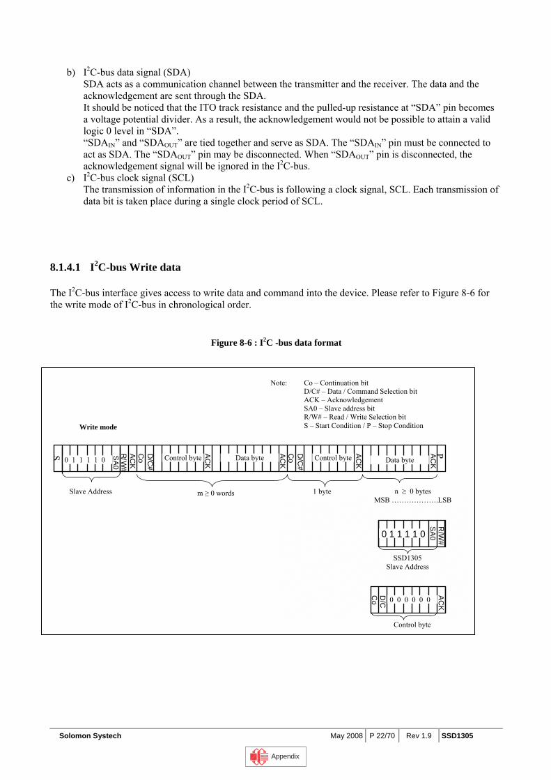
Solomon Systech May 2008 P 22/70 Rev 1.9 SSD1305
b) I2C-bus data signal (SDA) SDA acts as a communication channel between the transmitter and the receiver. The data and the acknowledgement are sent through the SDA. It should be noticed that the ITO track resistance and the pulled-up resistance at “SDA” pin becomes a voltage potential divider. As a result, the acknowledgement would not be possible to attain a valid logic 0 level in “SDA”. “SDAIN” and “SDAOUT” are tied together and serve as SDA. The “SDAIN” pin must be connected to act as SDA. The “SDAOUT” pin may be disconnected. When “SDAOUT” pin is disconnected, the acknowledgement signal will be ignored in the I2C-bus.
c) I2C-bus clock signal (SCL) The transmission of information in the I2C-bus is following a clock signal, SCL. Each transmission of data bit is taken place during a single clock period of SCL.
8.1.4.1 I2C-bus Write data The I2C-bus interface gives access to write data and command into the device. Please refer to Figure 8-6 for the write mode of I2C-bus in chronological order.
Figure 8-6 : I2C -bus data format
0 1 1 1 1
SA
0
P
Slave Address m ≥ 0 words n ≥ 0 bytes MSB ……………….LSB
1 byte
Write mode
SSD1305 Slave Address
R/W
#
D/C
#C
oA
CK
AC
KControl byte Data byte Control byte
AC
K Data byte
AC
K
S
0 1 1 1 1 0
SA
0 R
/W#
Co
D/C
AC
K
Control byte
Note: Co – Continuation bit D/C# – Data / Command Selection bit ACK – Acknowledgement SA0 – Slave address bit R/W# – Read / Write Selection bit S – Start Condition / P – Stop Condition
0 0 0 0 0 0
0 1 1 1 1 0
D/C
#C
oA
CK
Appendix
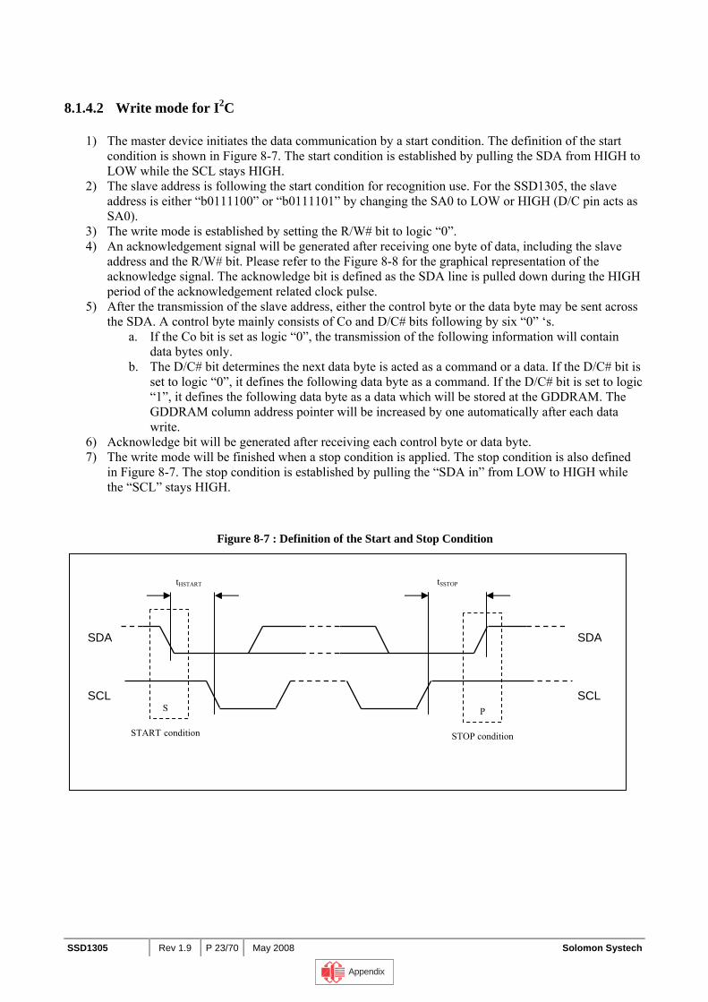
SSD1305 Rev 1.9 P 23/70 May 2008 Solomon Systech
S
START condition
SDA
SCL
P
STOP condition
SDA
SCL
tHSTART tSSTOP
8.1.4.2 Write mode for I2C
1) The master device initiates the data communication by a start condition. The definition of the start condition is shown in Figure 8-7. The start condition is established by pulling the SDA from HIGH to LOW while the SCL stays HIGH.
2) The slave address is following the start condition for recognition use. For the SSD1305, the slave address is either “b0111100” or “b0111101” by changing the SA0 to LOW or HIGH (D/C pin acts as SA0).
3) The write mode is established by setting the R/W# bit to logic “0”. 4) An acknowledgement signal will be generated after receiving one byte of data, including the slave
address and the R/W# bit. Please refer to the Figure 8-8 for the graphical representation of the acknowledge signal. The acknowledge bit is defined as the SDA line is pulled down during the HIGH period of the acknowledgement related clock pulse.
5) After the transmission of the slave address, either the control byte or the data byte may be sent across the SDA. A control byte mainly consists of Co and D/C# bits following by six “0” ‘s.
a. If the Co bit is set as logic “0”, the transmission of the following information will contain data bytes only.
b. The D/C# bit determines the next data byte is acted as a command or a data. If the D/C# bit is set to logic “0”, it defines the following data byte as a command. If the D/C# bit is set to logic “1”, it defines the following data byte as a data which will be stored at the GDDRAM. The GDDRAM column address pointer will be increased by one automatically after each data write.
6) Acknowledge bit will be generated after receiving each control byte or data byte. 7) The write mode will be finished when a stop condition is applied. The stop condition is also defined
in Figure 8-7. The stop condition is established by pulling the “SDA in” from LOW to HIGH while the “SCL” stays HIGH.
Figure 8-7 : Definition of the Start and Stop Condition
Appendix
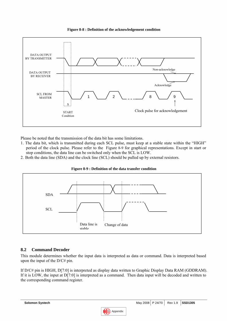
Solomon Systech May 2008 P 24/70 Rev 1.9 SSD1305
Figure 8-8 : Definition of the acknowledgement condition
Please be noted that the transmission of the data bit has some limitations. 1. The data bit, which is transmitted during each SCL pulse, must keep at a stable state within the “HIGH”
period of the clock pulse. Please refer to the Figure 8-9 for graphical representations. Except in start or stop conditions, the data line can be switched only when the SCL is LOW.
2. Both the data line (SDA) and the clock line (SCL) should be pulled up by external resistors.
Figure 8-9 : Definition of the data transfer condition
8.2 Command Decoder This module determines whether the input data is interpreted as data or command. Data is interpreted based upon the input of the D/C# pin. If D/C# pin is HIGH, D[7:0] is interpreted as display data written to Graphic Display Data RAM (GDDRAM). If it is LOW, the input at D[7:0] is interpreted as a command. Then data input will be decoded and written to the corresponding command register.
DATA OUTPUT BY RECEIVER
DATA OUTPUT BY TRANSMITTER
SCL FROM MASTER
S
START Condition
Clock pulse for acknowledgement
1 8 9
Non-acknowledge
2
Acknowledge
Data line is stable
SDA
SCL
Change of data
Appendix
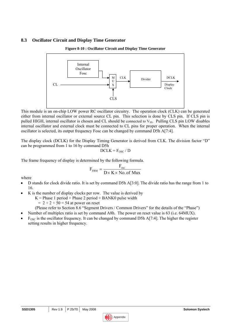
SSD1305 Rev 1.9 P 25/70 May 2008 Solomon Systech
8.3 Oscillator Circuit and Display Time Generator
Figure 8-10 : Oscillator Circuit and Display Time Generator
Divider
InternalOscillator
FoscMUXCL
CLK DCLK
DisplayClock
CLS
This module is an on-chip LOW power RC oscillator circuitry. The operation clock (CLK) can be generated either from internal oscillator or external source CL pin. This selection is done by CLS pin. If CLS pin is pulled HIGH, internal oscillator is chosen and CL should be connected to VSS. Pulling CLS pin LOW disables internal oscillator and external clock must be connected to CL pins for proper operation. When the internal oscillator is selected, its output frequency Fosc can be changed by command D5h A[7:4]. The display clock (DCLK) for the Display Timing Generator is derived from CLK. The division factor “D” can be programmed from 1 to 16 by command D5h
DCLK = FOSC / D The frame frequency of display is determined by the following formula.
MuxofNo.K DF
F oscFRM ××
=
where • D stands for clock divide ratio. It is set by command D5h A[3:0]. The divide ratio has the range from 1 to
16. • K is the number of display clocks per row. The value is derived by
K = Phase 1 period + Phase 2 period + BANK0 pulse width = 2 + 2 + 50 = 54 at power on reset (Please refer to Section 8.6 “Segment Drivers / Common Drivers” for the details of the “Phase”)
• Number of multiplex ratio is set by command A8h. The power on reset value is 63 (i.e. 64MUX). • FOSC is the oscillator frequency. It can be changed by command D5h A[7:4]. The higher the register
setting results in higher frequency.
Appendix
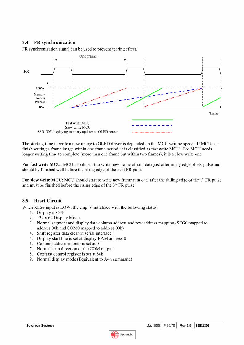
Solomon Systech May 2008 P 26/70 Rev 1.9 SSD1305
8.4 FR synchronization FR synchronization signal can be used to prevent tearing effect.
The starting time to write a new image to OLED driver is depended on the MCU writing speed. If MCU can finish writing a frame image within one frame period, it is classified as fast write MCU. For MCU needs longer writing time to complete (more than one frame but within two frames), it is a slow write one. For fast write MCU: MCU should start to write new frame of ram data just after rising edge of FR pulse and should be finished well before the rising edge of the next FR pulse. For slow write MCU: MCU should start to write new frame ram data after the falling edge of the 1st FR pulse and must be finished before the rising edge of the 3rd FR pulse.
8.5 Reset Circuit When RES# input is LOW, the chip is initialized with the following status:
1. Display is OFF 2. 132 x 64 Display Mode 3. Normal segment and display data column address and row address mapping (SEG0 mapped to
address 00h and COM0 mapped to address 00h) 4. Shift register data clear in serial interface 5. Display start line is set at display RAM address 0 6. Column address counter is set at 0 7. Normal scan direction of the COM outputs 8. Contrast control register is set at 80h 9. Normal display mode (Equivalent to A4h command)
Fast write MCU Slow write MCU
SSD1305 displaying memory updates to OLED screen
One frame
FR
100%
0%
Memory Access Process
Time
Appendix
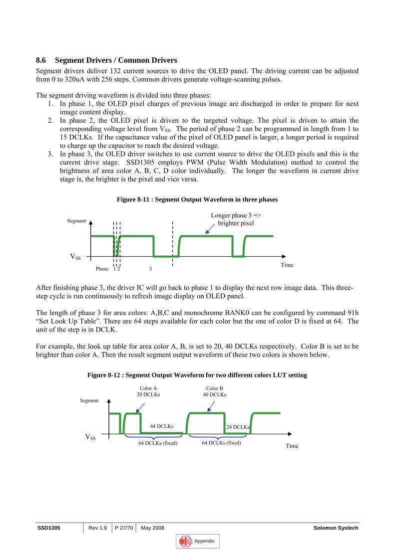
SSD1305 Rev 1.9 P 27/70 May 2008 Solomon Systech
8.6 Segment Drivers / Common Drivers Segment drivers deliver 132 current sources to drive the OLED panel. The driving current can be adjusted from 0 to 320uA with 256 steps. Common drivers generate voltage-scanning pulses. The segment driving waveform is divided into three phases:
1. In phase 1, the OLED pixel charges of previous image are discharged in order to prepare for next image content display.
2. In phase 2, the OLED pixel is driven to the targeted voltage. The pixel is driven to attain the corresponding voltage level from VSS. The period of phase 2 can be programmed in length from 1 to 15 DCLKs. If the capacitance value of the pixel of OLED panel is larger, a longer period is required to charge up the capacitor to reach the desired voltage.
3. In phase 3, the OLED driver switches to use current source to drive the OLED pixels and this is the current drive stage. SSD1305 employs PWM (Pulse Width Modulation) method to control the brightness of area color A, B, C, D color individually. The longer the waveform in current drive stage is, the brighter is the pixel and vice versa.
Figure 8-11 : Segment Output Waveform in three phases
After finishing phase 3, the driver IC will go back to phase 1 to display the next row image data. This three-step cycle is run continuously to refresh image display on OLED panel. The length of phase 3 for area colors: A,B,C and monochrome BANK0 can be configured by command 91h “Set Look Up Table”. There are 64 steps available for each color but the one of color D is fixed at 64. The unit of the step is in DCLK. For example, the look up table for area color A, B, is set to 20, 40 DCLKs respectively. Color B is set to be brighter than color A. Then the result segment output waveform of these two colors is shown below.
Figure 8-12 : Segment Output Waveform for two different colors LUT setting
Segment
VSS
Phase: 1 2 3
Longer phase 3 => brighter pixel
Segment
VSS
Color A 20 DCLKs
64 DCLKs (fixed)
44 DCLKs 24 DCLKs
64 DCLKs (fixed)
Color B 40 DCLKs
Time
Time
Appendix
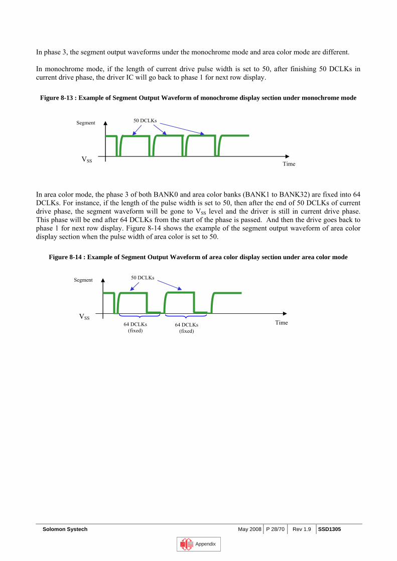
Solomon Systech May 2008 P 28/70 Rev 1.9 SSD1305
In phase 3, the segment output waveforms under the monochrome mode and area color mode are different. In monochrome mode, if the length of current drive pulse width is set to 50, after finishing 50 DCLKs in current drive phase, the driver IC will go back to phase 1 for next row display.
Figure 8-13 : Example of Segment Output Waveform of monochrome display section under monochrome mode
In area color mode, the phase 3 of both BANK0 and area color banks (BANK1 to BANK32) are fixed into 64 DCLKs. For instance, if the length of the pulse width is set to 50, then after the end of 50 DCLKs of current drive phase, the segment waveform will be gone to VSS level and the driver is still in current drive phase. This phase will be end after 64 DCLKs from the start of the phase is passed. And then the drive goes back to phase 1 for next row display. Figure 8-14 shows the example of the segment output waveform of area color display section when the pulse width of area color is set to 50.
Figure 8-14 : Example of Segment Output Waveform of area color display section under area color mode
Segment
VSS
50 DCLKs
Segment
VSS
50 DCLKs
64 DCLKs (fixed)
64 DCLKs (fixed)
Time
Time
Appendix
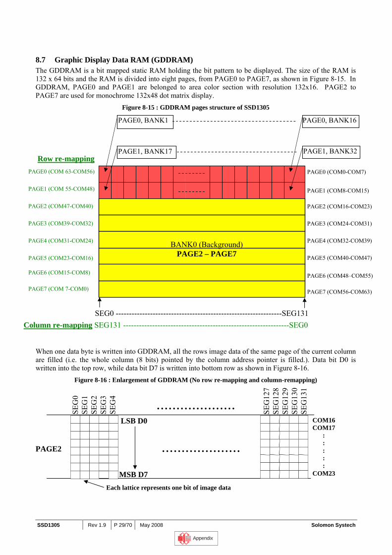
SSD1305 Rev 1.9 P 29/70 May 2008 Solomon Systech
8.7 Graphic Display Data RAM (GDDRAM) The GDDRAM is a bit mapped static RAM holding the bit pattern to be displayed. The size of the RAM is 132 x 64 bits and the RAM is divided into eight pages, from PAGE0 to PAGE7, as shown in Figure 8-15. In GDDRAM, PAGE0 and PAGE1 are belonged to area color section with resolution 132x16. PAGE2 to PAGE7 are used for monochrome 132x48 dot matrix display.
Figure 8-15 : GDDRAM pages structure of SSD1305
When one data byte is written into GDDRAM, all the rows image data of the same page of the current column are filled (i.e. the whole column (8 bits) pointed by the column address pointer is filled.). Data bit D0 is written into the top row, while data bit D7 is written into bottom row as shown in Figure 8-16.
Figure 8-16 : Enlargement of GDDRAM (No row re-mapping and column-remapping)
PAGE0, BANK1 PAGE0, BANK16
PAGE1, BANK17 PAGE1, BANK32
BANK0 (Background) PAGE2 – PAGE7
Row re-mapping PAGE0 (COM 63-COM56)
PAGE1 (COM 55-COM48)
PAGE2 (COM47-COM40)
PAGE3 (COM39-COM32)
PAGE4 (COM31-COM24)
PAGE5 (COM23-COM16)
PAGE6 (COM15-COM8)
PAGE7 (COM 7-COM0)
PAGE0 (COM0-COM7)
PAGE1 (COM8-COM15)
PAGE2 (COM16-COM23)
PAGE3 (COM24-COM31)
PAGE4 (COM32-COM39)
PAGE5 (COM40-COM47)
PAGE6 (COM48–COM55) PAGE7 (COM56-COM63)
SEG0 ---------------------------------------------------------------SEG131 Column re-mapping SEG131 ---------------------------------------------------------------SEG0
LSB D0
MSB D7
Each lattice represents one bit of image data
....................PAGE2
COM16COM17
: : : : :
COM23
SEG
0 SE
G1
SEG
2 SE
G3
SEG
4
SEG
127
SEG
128
SEG
129
SEG
130
SEG
131
....................
Appendix
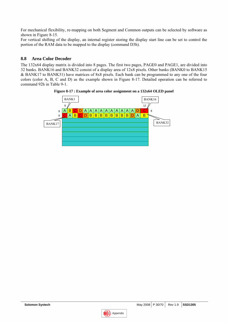
Solomon Systech May 2008 P 30/70 Rev 1.9 SSD1305
For mechanical flexibility, re-mapping on both Segment and Common outputs can be selected by software as shown in Figure 8-15. For vertical shifting of the display, an internal register storing the display start line can be set to control the portion of the RAM data to be mapped to the display (command D3h).
8.8 Area Color Decoder The 132x64 display matrix is divided into 8 pages. The first two pages, PAGE0 and PAGE1, are divided into 32 banks. BANK16 and BANK32 consist of a display area of 12x8 pixels. Other banks (BANK0 to BANK15 & BANK17 to BANK31) have matrices of 8x8 pixels. Each bank can be programmed to any one of the four colors (color A, B, C and D) as the example shown in Figure 8-17. Detailed operation can be referred to command 92h in Table 9-1.
Figure 8-17 : Example of area color assignment on a 132x64 OLED panel
A B C D A A A A A A A A A A D CC A B C D B B B B B B B B D A B
8
8
12
8
8
BANK1 BANK16
BANK32BANK17
Appendix
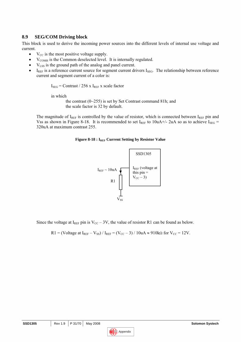
SSD1305 Rev 1.9 P 31/70 May 2008 Solomon Systech
8.9 SEG/COM Driving block This block is used to derive the incoming power sources into the different levels of internal use voltage and current.
• VCC is the most positive voltage supply. • VCOMH is the Common deselected level. It is internally regulated. • VLSS is the ground path of the analog and panel current. • IREF is a reference current source for segment current drivers ISEG. The relationship between reference
current and segment current of a color is:
ISEG = Contrast / 256 x IREF x scale factor in which
the contrast (0~255) is set by Set Contrast command 81h; and the scale factor is 32 by default.
The magnitude of IREF is controlled by the value of resistor, which is connected between IREF pin and Vss as shown in Figure 8-18. It is recommended to set IREF to 10uA+/- 2uA so as to achieve ISEG = 320uA at maximum contrast 255.
Figure 8-18 : IREF Current Setting by Resistor Value
Since the voltage at IREF pin is VCC – 3V, the value of resistor R1 can be found as below.
R1 = (Voltage at IREF – VSS) / IREF = (VCC – 3) / 10uA ≈ 910kΩ for VCC = 12V.
SSD1305
IREF (voltage at this pin = VCC – 3)
R1
VSS
IREF ~ 10uA
Appendix
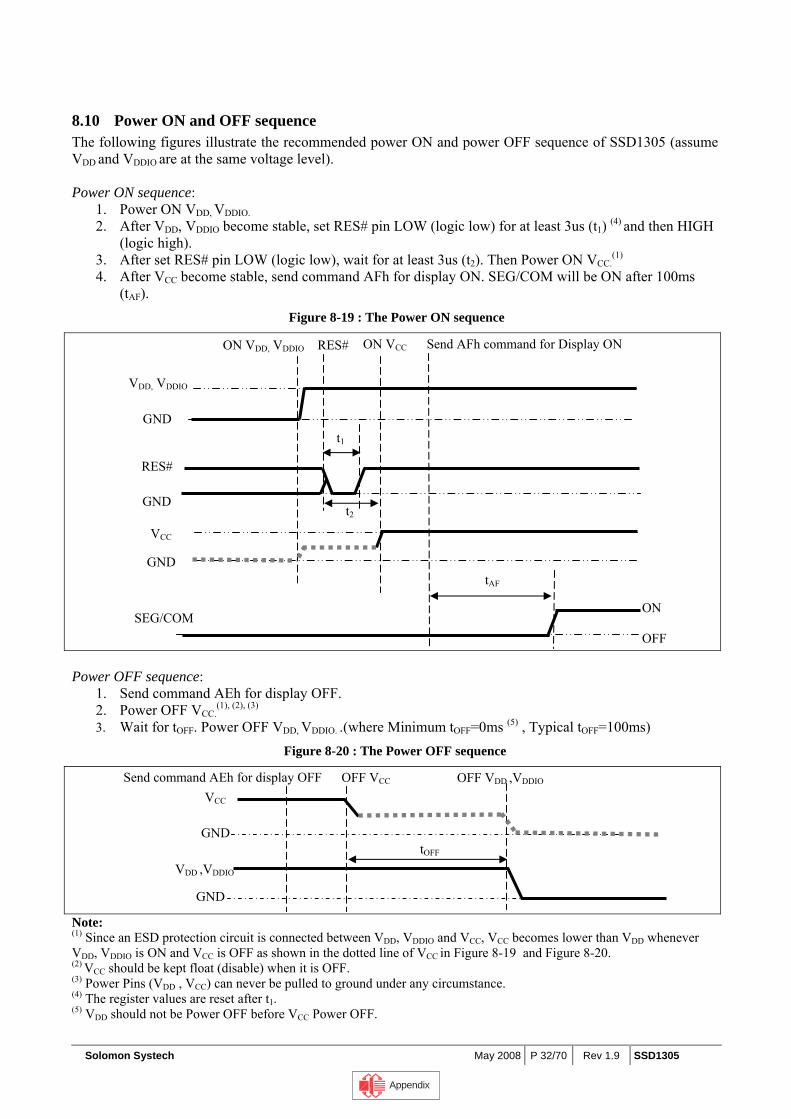
Solomon Systech May 2008 P 32/70 Rev 1.9 SSD1305
8.10 Power ON and OFF sequence The following figures illustrate the recommended power ON and power OFF sequence of SSD1305 (assume VDD and VDDIO are at the same voltage level). Power ON sequence:
1. Power ON VDD, VDDIO. 2. After VDD, VDDIO become stable, set RES# pin LOW (logic low) for at least 3us (t1) (4) and then HIGH
(logic high). 3. After set RES# pin LOW (logic low), wait for at least 3us (t2). Then Power ON VCC.
(1) 4. After VCC become stable, send command AFh for display ON. SEG/COM will be ON after 100ms
(tAF). Figure 8-19 : The Power ON sequence
Power OFF sequence:
1. Send command AEh for display OFF. 2. Power OFF VCC.
(1), (2), (3) 3. Wait for tOFF. Power OFF VDD, VDDIO. .(where Minimum tOFF=0ms (5) , Typical tOFF=100ms)
Figure 8-20 : The Power OFF sequence
Note: (1) Since an ESD protection circuit is connected between VDD, VDDIO and VCC, VCC becomes lower than VDD whenever VDD, VDDIO is ON and VCC is OFF as shown in the dotted line of VCC in Figure 8-19 and Figure 8-20. (2)
VCC should be kept float (disable) when it is OFF. (3) Power Pins (VDD , VCC) can never be pulled to ground under any circumstance. (4) The register values are reset after t1. (5) VDD should not be Power OFF before VCC Power OFF.
OFF VDD ,VDDIO
VDD ,VDDIO
VCC Send command AEh for display OFF OFF VCC
GND
GND tOFF
GND
ON VDD, VDDIO RES# ON VCC Send AFh command for Display ON
VDD, VDDIO
RES#
GND
t1
SEG/COM
tAF
ON OFF
VCC
GND t2
Appendix
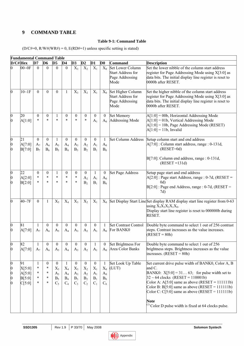
SSD1305 Rev 1.9 P 33/70 May 2008 Solomon Systech
9 COMMAND TABLE
Table 9-1: Command Table
(D/C#=0, R/W#(WR#) = 0, E(RD#=1) unless specific setting is stated)
Fundamental Command Table D/C# Hex D7 D6 D5 D4 D3 D2 D1 D0 Command Description 0 00~0F 0 0 0 0 X3 X2 X1 X0
Set Lower Column Start Address for Page Addressing Mode
Set the lower nibble of the column start address register for Page Addressing Mode using X[3:0] as data bits. The initial display line register is reset to 0000b after RESET.
0 10~1F 0 0 0 1 X3 X2 X1 X0
Set Higher Column Start Address for Page Addressing Mode
Set the higher nibble of the column start address register for Page Addressing Mode using X[3:0] as data bits. The initial display line register is reset to 0000b after RESET.
0 20 0 0 1 0 0 0 0 00 A[1:0] * * * * * * A1 A0
Set Memory Addressing Mode
A[1:0] = 00b, Horizontal Addressing Mode A[1:0] = 01b, Vertical Addressing Mode A[1:0] = 10b, Page Addressing Mode (RESET) A[1:0] = 11b, Invalid
0 21 0 0 1 0 0 0 0 10 A[7:0] A7 A6 A5 A4 A3 A2 A1 A00 B[7:0] B7 B6 B5 B4 B3 B2 B1 B0
Set Column Address Setup column start and end address A[7:0] : Column start address, range : 0-131d,
(RESET=0d) B[7:0]: Column end address, range : 0-131d,
(RESET =131d)
0 22 0 0 1 0 0 0 1 00 A[2:0] * * * * * A2 A1 A00 B[2:0] * * * * * B2 B1 B0
Set Page Address Setup page start and end address A[2:0] : Page start Address, range : 0-7d, (RESET =
0d) B[2:0] : Page end Address, range : 0-7d, (RESET =
7d)
0 40~7F 0 1 X5 X4 X3 X2 X1 X0
Set Display Start Line Set display RAM display start line register from 0-63 using X5X3X2X1X0. Display start line register is reset to 000000b during RESET.
0 81 1 0 0 0 0 0 0 10 A[7:0] A7 A6 A5 A4 A3 A2 A1 A0
Set Contrast Control For BANK0
Double byte command to select 1 out of 256 contrast steps. Contrast increases as the value increases. (RESET = 80h)
0 82 1 0 0 0 0 0 1 00 A[7:0] A7 A6 A5 A4 A3 A2 A1 A0
Set Brightness For Area Color Banks
Double byte command to select 1 out of 256 brightness steps. Brightness increases as the value increases. (RESET = 80h)
0 91 1 0 0 1 0 0 0 10 X[5:0] * * X5 X4 X3 X2 X1 X00 A[5:0] * * A5 A4 A3 A2 A1 A00 B[5:0] * * B5 B4 B3 B2 B1 B00 C[5:0] * * C5 C4 C3 C2 C1 C0
Set Look Up Table (LUT)
Set current drive pulse width of BANK0, Color A, B and C. BANK0: X[5:0] = 31… 63; for pulse width set to 32 ~ 64 clocks (RESET = 110001b) Color A: A[5:0] same as above (RESET = 111111b) Color B: B[5:0] same as above (RESET = 111111b) Color C: C[5:0] same as above (RESET = 111111b) Note (1) Color D pulse width is fixed at 64 clocks pulse.
Appendix
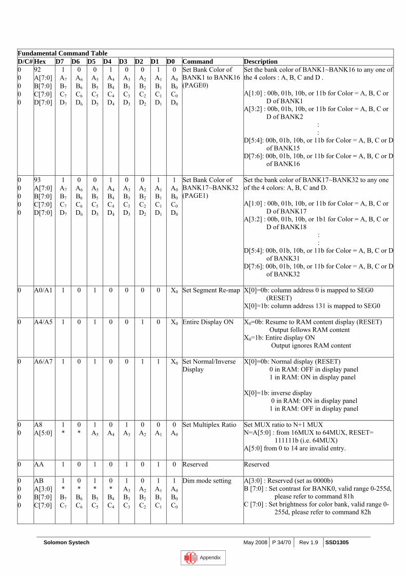
Solomon Systech May 2008 P 34/70 Rev 1.9 SSD1305
Fundamental Command Table D/C# Hex D7 D6 D5 D4 D3 D2 D1 D0 Command Description 0 92 1 0 0 1 0 0 1 00 A[7:0] A7 A6 A5 A4 A3 A2 A1 A00 B[7:0] B7 B6 B5 B4 B3 B2 B1 B00 C[7:0] C7 C6 C5 C4 C3 C2 C1 C00 D[7:0] D7 D6 D5 D4 D3 D2 D1 D0
Set Bank Color of BANK1 to BANK16 (PAGE0)
Set the bank color of BANK1~BANK16 to any one of the 4 colors : A, B, C and D . A[1:0] : 00b, 01b, 10b, or 11b for Color = A, B, C or
D of BANK1 A[3:2] : 00b, 01b, 10b, or 11b for Color = A, B, C or
D of BANK2 : : D[5:4]: 00b, 01b, 10b, or 11b for Color = A, B, C or D
of BANK15 D[7:6]: 00b, 01b, 10b, or 11b for Color = A, B, C or D
of BANK16
0 93 1 0 0 1 0 0 1 10 A[7:0] A7 A6 A5 A4 A3 A2 A1 A00 B[7:0] B7 B6 B5 B4 B3 B2 B1 B00 C[7:0] C7 C6 C5 C4 C3 C2 C1 C00 D[7:0] D7 D6 D5 D4 D3 D2 D1 D0
Set Bank Color of BANK17~BANK32 (PAGE1)
Set the bank color of BANK17~BANK32 to any one of the 4 colors: A, B, C and D. A[1:0] : 00b, 01b, 10b, or 11b for Color = A, B, C or
D of BANK17 A[3:2] : 00b, 01b, 10b, or 1b1 for Color = A, B, C or
D of BANK18 : :
D[5:4]: 00b, 01b, 10b, or 11b for Color = A, B, C or D of BANK31
D[7:6]: 00b, 01b, 10b, or 11b for Color = A, B, C or D of BANK32
0 A0/A1 1 0 1 0 0 0 0 X0
Set Segment Re-map X[0]=0b: column address 0 is mapped to SEG0 (RESET)
X[0]=1b: column address 131 is mapped to SEG0
0 A4/A5 1 0 1 0 0 1 0 X0 Entire Display ON X0=0b: Resume to RAM content display (RESET) Output follows RAM content X0=1b: Entire display ON Output ignores RAM content
0 A6/A7 1 0 1 0 0 1 1 X0
Set Normal/Inverse Display
X[0]=0b: Normal display (RESET) 0 in RAM: OFF in display panel 1 in RAM: ON in display panel X[0]=1b: inverse display 0 in RAM: ON in display panel 1 in RAM: OFF in display panel
0 A8 1 0 1 0 1 0 0 00 A[5:0] * * A5 A4 A3 A2 A1 A0
Set Multiplex Ratio Set MUX ratio to N+1 MUX N=A[5:0] : from 16MUX to 64MUX, RESET=
111111b (i.e. 64MUX) A[5:0] from 0 to 14 are invalid entry.
0 AA 1 0 1 0 1 0 1 0
Reserved Reserved
0 AB 1 0 1 0 1 0 1 10 A[3:0] * * * * A3 A2 A1 A00 B[7:0] B7 B6 B5 B4 B3 B2 B1 B00 C[7:0] C7 C6 C5 C4 C3 C2 C1 C0
Dim mode setting A[3:0] : Reserved (set as 0000b) B [7:0] : Set contrast for BANK0, valid range 0-255d,
please refer to command 81h C [7:0] : Set brightness for color bank, valid range 0-
255d, please refer to command 82h
Appendix
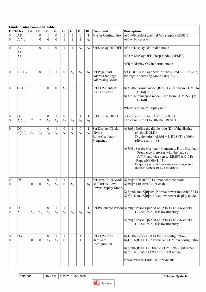
SSD1305 Rev 1.9 P 35/70 May 2008 Solomon Systech
Fundamental Command Table D/C# Hex D7 D6 D5 D4 D3 D2 D1 D0 Command Description 0 AD 1 0 1 0 1 1 0 10 A[7:0] 1 0 0 0 1 1 1 A0
Master Configuration A[0]=0b, Select external VCC supply (RESET) A[0]=1b, Reserved
0 AC 1 0 1 0 1 1 A1 A0 AE AF
Set Display ON/OFF
ACh = Display ON in dim mode AEh = Display OFF (sleep mode) (RESET) AFh = Display ON in normal mode
0 B0~B7 1 0 1 1 0 X2 X1 X0
Set Page Start Address for Page Addressing Mode
Set GDDRAM Page Start Address (PAGE0~PAGE7) for Page Addressing Mode using X[2:0].
0 C0/C8 1 1 0 0 X3 0 0 0
Set COM Output Scan Direction
X[3]=0b: normal mode (RESET) Scan from COM0 to COM[N –1]
X[3]=1b: remapped mode. Scan from COM[N~1] to COM0
Where N is the Multiplex ratio.
0 D3 1 1 0 1 0 0 1 10 A[5:0] * * A5 A4 A3 A2 A1 A0
Set Display Offset Set vertical shift by COM from 0~63. The value is reset to 00h after RESET.
0 D5 1 1 0 1 0 1 0 1 A[7:0] A7 A6 A5 A4 A3 A2 A1 A0
Set Display Clock Divide Ratio/Oscillator Frequency
A[3:0] : Define the divide ratio (D) of the display clocks (DCLK): Divide ratio= A[3:0] + 1, RESET is 0000b (divide ratio = 1)
A[7:4] : Set the Oscillator Frequency, FOSC. Oscillator
Frequency increases with the value of A[7:4] and vice versa. RESET is 0111b
Range:0000b~1111b Frequency increases as setting value increases. Refer to section 10.1.23 for details.
0 D8 1 1 0 1 1 0 0 00 0 0 X5 X4 0 X2 0 X0
Set Area Color Mode ON/OFF & Low Power Display Mode
X[5:4]= 00b (RESET) : monochrome mode X[5:4]= 11b Area Color enable X[2]=0b and X[0]=0b: Normal power mode(RESET)X[2]=1b and X[0]=1b: Set low power display mode
0 D9 1 1 0 1 1 0 0 10 A[7:0] A7 A6 A5 A4 A3 A2 A1 A0
Set Pre-charge Period A[3:0] : Phase 1 period of up to 15 DCLK clocks (RESET=2h); 0 is invalid entry
A[7:4] : Phase 2 period of up to 15 DCLK clocks
(RESET=2h); 0 is invalid entry
0 DA 1 1 0 1 1 0 1 00 0 0 X5 X4 0 0 1 0
Set COM Pins Hardware Configuration
X[4]=0b, Sequential COM pin configuration X[4]=1b(RESET), Alternative COM pin configuration X[5]=0b(RESET), Disable COM Left/Right remap X[5]=1b, Enable COM Left/Right remap Please refer to Table 10-3 for details.
Appendix
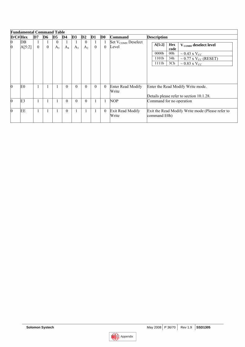
Solomon Systech May 2008 P 36/70 Rev 1.9 SSD1305
Fundamental Command Table D/C# Hex D7 D6 D5 D4 D3 D2 D1 D0 Command Description 0 DB 1 1 0 1 1 0 1 10 A[5:2] 0 0 A5 A4 A3 A2 0 0
Set VCOMH Deselect Level
A[5:2] Hex code
V COMH deselect level
0000b 00h ~ 0.43 x VCC 1101b 34h ~ 0.77 x VCC (RESET) 1111b 3Ch ~ 0.83 x VCC
0 E0 1 1 1 0 0 0 0 0
Enter Read Modify Write
Enter the Read Modify Write mode. Details please refer to section 10.1.28.
0 E3 1 1 1 0 0 0 1 1
NOP Command for no operation
0 EE 1 1 1 0 1 1 1 0
Exit Read Modify Write
Exit the Read Modify Write mode (Please refer to command E0h)
Appendix
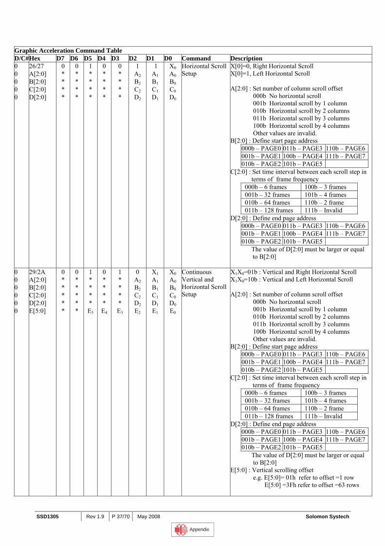
SSD1305 Rev 1.9 P 37/70 May 2008 Solomon Systech
Graphic Acceleration Command Table D/C#Hex D7 D6 D5 D4 D3 D2 D1 D0 Command Description 0 26/27 0 0 1 0 0 1 1 X0 0 A[2:0] * * * * * A2 A1 A00 B[2:0] * * * * * B2 B1 B00 C[2:0] * * * * * C2 C1 C00 D[2:0] * * * * * D2 D1 D0
Horizontal Scroll Setup
X[0]=0, Right Horizontal Scroll X[0]=1, Left Horizontal Scroll A[2:0] : Set number of column scroll offset 000b No horizontal scroll 001b Horizontal scroll by 1 column 010b Horizontal scroll by 2 columns 011b Horizontal scroll by 3 columns 100b Horizontal scroll by 4 columns Other values are invalid. B[2:0] : Define start page address
000b – PAGE0 011b – PAGE3 110b – PAGE6001b – PAGE1 100b – PAGE4 111b – PAGE7010b – PAGE2 101b – PAGE5
C[2:0] : Set time interval between each scroll step in terms of frame frequency
000b – 6 frames 100b – 3 frames 001b – 32 frames 101b – 4 frames 010b – 64 frames 110b – 2 frame 011b – 128 frames 111b – Invalid
D[2:0] : Define end page address 000b – PAGE0 011b – PAGE3 110b – PAGE6001b – PAGE1 100b – PAGE4 111b – PAGE7010b – PAGE2 101b – PAGE5
The value of D[2:0] must be larger or equal to B[2:0]
0 29/2A 0 0 1 0 1 0 X1 X00 A[2:0] * * * * * A2 A1 A00 B[2:0] * * * * * B2 B1 B00 C[2:0] * * * * * C2 C1 C00 D[2:0] * * * * * D2 D1 D00 E[5:0] * * E5 E4 E3 E2 E1 E0
Continuous Vertical and Horizontal Scroll Setup
X1X0=01b : Vertical and Right Horizontal Scroll X1X0=10b : Vertical and Left Horizontal Scroll A[2:0] : Set number of column scroll offset 000b No horizontal scroll 001b Horizontal scroll by 1 column 010b Horizontal scroll by 2 columns 011b Horizontal scroll by 3 columns 100b Horizontal scroll by 4 columns Other values are invalid. B[2:0] : Define start page address
000b – PAGE0 011b – PAGE3 110b – PAGE6001b – PAGE1 100b – PAGE4 111b – PAGE7010b – PAGE2 101b – PAGE5
C[2:0] : Set time interval between each scroll step in terms of frame frequency
000b – 6 frames 100b – 3 frames 001b – 32 frames 101b – 4 frames 010b – 64 frames 110b – 2 frame 011b – 128 frames 111b – Invalid
D[2:0] : Define end page address 000b – PAGE0 011b – PAGE3 110b – PAGE6001b – PAGE1 100b – PAGE4 111b – PAGE7010b – PAGE2 101b – PAGE5
The value of D[2:0] must be larger or equal to B[2:0] E[5:0] : Vertical scrolling offset e.g. E[5:0]= 01h refer to offset =1 row E[5:0] =3Fh refer to offset =63 rows
Appendix
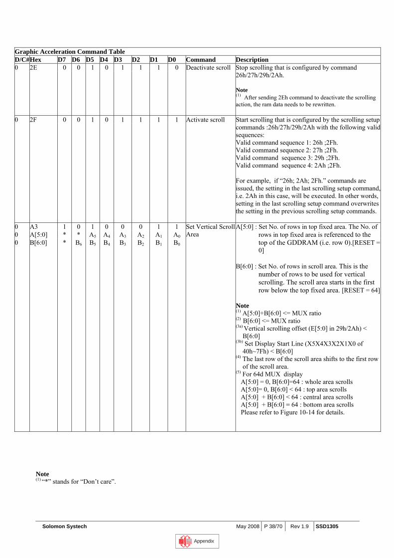
Solomon Systech May 2008 P 38/70 Rev 1.9 SSD1305
Graphic Acceleration Command Table D/C#Hex D7 D6 D5 D4 D3 D2 D1 D0 Command Description 0 2E 0 0 1 0 1 1 1 0
Deactivate scroll Stop scrolling that is configured by command 26h/27h/29h/2Ah. Note (1) After sending 2Eh command to deactivate the scrolling action, the ram data needs to be rewritten.
0 2F 0 0 1 0 1 1 1 1
Activate scroll Start scrolling that is configured by the scrolling setup commands :26h/27h/29h/2Ah with the following valid sequences: Valid command sequence 1: 26h ;2Fh. Valid command sequence 2: 27h ;2Fh. Valid command sequence 3: 29h ;2Fh. Valid command sequence 4: 2Ah ;2Fh. For example, if “26h; 2Ah; 2Fh.” commands are issued, the setting in the last scrolling setup command, i.e. 2Ah in this case, will be executed. In other words, setting in the last scrolling setup command overwrites the setting in the previous scrolling setup commands.
0 A3 1 0 1 0 0 0 1 1 0 A[5:0] * * A5 A4 A3 A2 A1 A00 B[6:0] * B6 B5 B4 B3 B2 B1 B0
Set Vertical Scroll Area
A[5:0] : Set No. of rows in top fixed area. The No. of rows in top fixed area is referenced to the top of the GDDRAM (i.e. row 0).[RESET = 0]
B[6:0] : Set No. of rows in scroll area. This is the
number of rows to be used for vertical scrolling. The scroll area starts in the first row below the top fixed area. [RESET = 64]
Note (1) A[5:0]+B[6:0] <= MUX ratio (2) B[6:0] <= MUX ratio (3a) Vertical scrolling offset (E[5:0] in 29h/2Ah) <
B[6:0] (3b) Set Display Start Line (X5X4X3X2X1X0 of
40h~7Fh) < B[6:0] (4) The last row of the scroll area shifts to the first row
of the scroll area. (5) For 64d MUX display A[5:0] = 0, B[6:0]=64 : whole area scrolls A[5:0]= 0, B[6:0] < 64 : top area scrolls A[5:0] + B[6:0] < 64 : central area scrolls A[5:0] + B[6:0] = 64 : bottom area scrolls Please refer to Figure 10-14 for details.
Note (1) “*” stands for “Don’t care”.
Appendix
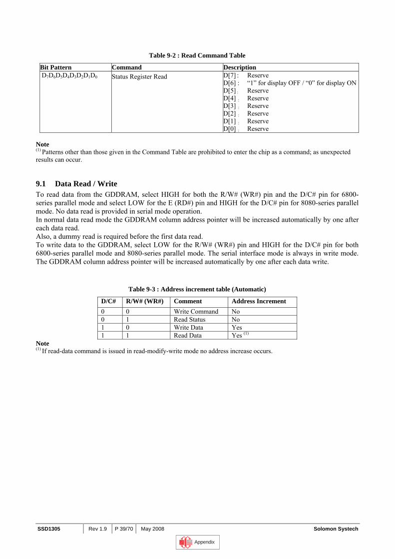
SSD1305 Rev 1.9 P 39/70 May 2008 Solomon Systech
Table 9-2 : Read Command Table
Bit Pattern Command Description D7D6D5D4D3D2D1D0
Status Register Read
D[7] : Reserve D[6] : “1” for display OFF / “0” for display OND[5] : Reserve D[4] : Reserve D[3] : Reserve D[2] : Reserve D[1] : Reserve D[0] : Reserve
Note (1) Patterns other than those given in the Command Table are prohibited to enter the chip as a command; as unexpected results can occur.
9.1 Data Read / Write To read data from the GDDRAM, select HIGH for both the R/W# (WR#) pin and the D/C# pin for 6800-series parallel mode and select LOW for the E (RD#) pin and HIGH for the D/C# pin for 8080-series parallel mode. No data read is provided in serial mode operation. In normal data read mode the GDDRAM column address pointer will be increased automatically by one after each data read. Also, a dummy read is required before the first data read. To write data to the GDDRAM, select LOW for the R/W# (WR#) pin and HIGH for the D/C# pin for both 6800-series parallel mode and 8080-series parallel mode. The serial interface mode is always in write mode. The GDDRAM column address pointer will be increased automatically by one after each data write.
Table 9-3 : Address increment table (Automatic)
D/C# R/W# (WR#) Comment Address Increment 0 0 Write Command No 0 1 Read Status No 1 0 Write Data Yes 1 1 Read Data Yes (1)
Note (1) If read-data command is issued in read-modify-write mode no address increase occurs.
Appendix
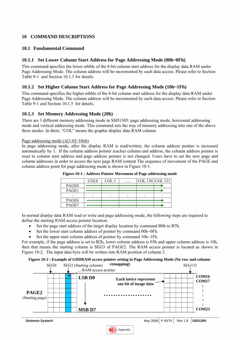
Solomon Systech May 2008 P 40/70 Rev 1.9 SSD1305
10 COMMAND DESCRIPTIONS
10.1 Fundamental Command
10.1.1 Set Lower Column Start Address for Page Addressing Mode (00h~0Fh) This command specifies the lower nibble of the 8-bit column start address for the display data RAM under Page Addressing Mode. The column address will be incremented by each data access. Please refer to Section Table 9-1 and Section 10.1.3 for details.
10.1.2 Set Higher Column Start Address for Page Addressing Mode (10h~1Fh) This command specifies the higher nibble of the 8-bit column start address for the display data RAM under Page Addressing Mode. The column address will be incremented by each data access. Please refer to Section Table 9-1 and Section 10.1.3 for details.
10.1.3 Set Memory Addressing Mode (20h) There are 3 different memory addressing mode in SSD1305: page addressing mode, horizontal addressing mode and vertical addressing mode. This command sets the way of memory addressing into one of the above three modes. In there, “COL” means the graphic display data RAM column. Page addressing mode (A[1:0]=10xb) In page addressing mode, after the display RAM is read/written, the column address pointer is increased automatically by 1. If the column address pointer reaches column end address, the column address pointer is reset to column start address and page address pointer is not changed. Users have to set the new page and column addresses in order to access the next page RAM content The sequence of movement of the PAGE and column address point for page addressing mode is shown in Figure 10-1.
Figure 10-1 : Address Pointer Movement of Page addressing mode COL0 COL 1 ….. COL 130 COL 131
PAGE0 PAGE1
: : : : : : PAGE6 PAGE7
In normal display data RAM read or write and page addressing mode, the following steps are required to define the starting RAM access pointer location:
• Set the page start address of the target display location by command B0h to B7h. • Set the lower start column address of pointer by command 00h~0Fh. • Set the upper start column address of pointer by command 10h~1Fh.
For example, if the page address is set to B2h, lower column address is 03h and upper column address is 10h, then that means the starting column is SEG3 of PAGE2. The RAM access pointer is located as shown in Figure 10-2. The input data byte will be written into RAM position of column 3.
Figure 10-2 : Example of GDDRAM access pointer setting in Page Addressing Mode (No row and column-remapping)
LSB D0
MSB D7
Each lattice represents one bit of image data
....................PAGE2 (Starting page)
COM16COM17
: : : : :
COM23
SEG0 SEG3 (Starting column) SEG131 RAM access pointer
Appendix
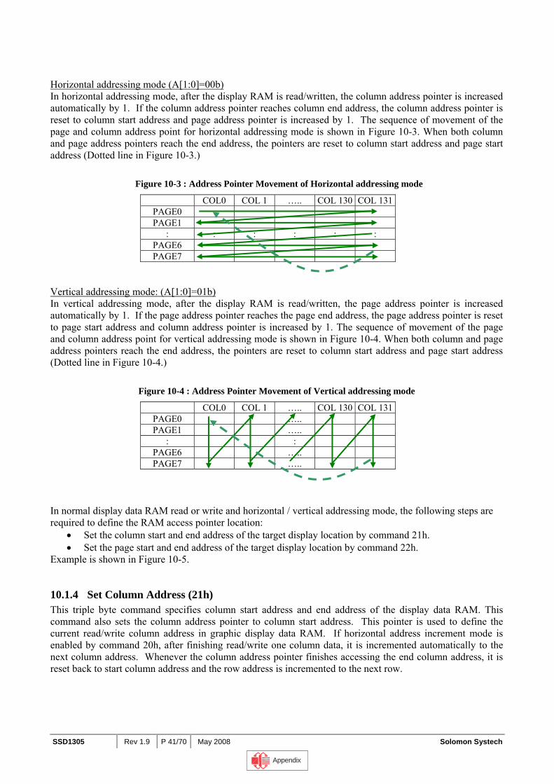
SSD1305 Rev 1.9 P 41/70 May 2008 Solomon Systech
Horizontal addressing mode (A[1:0]=00b) In horizontal addressing mode, after the display RAM is read/written, the column address pointer is increased automatically by 1. If the column address pointer reaches column end address, the column address pointer is reset to column start address and page address pointer is increased by 1. The sequence of movement of the page and column address point for horizontal addressing mode is shown in Figure 10-3. When both column and page address pointers reach the end address, the pointers are reset to column start address and page start address (Dotted line in Figure 10-3.)
Figure 10-3 : Address Pointer Movement of Horizontal addressing mode
COL0 COL 1 ….. COL 130 COL 131 PAGE0 PAGE1
: : : : : : PAGE6 PAGE7
Vertical addressing mode: (A[1:0]=01b) In vertical addressing mode, after the display RAM is read/written, the page address pointer is increased automatically by 1. If the page address pointer reaches the page end address, the page address pointer is reset to page start address and column address pointer is increased by 1. The sequence of movement of the page and column address point for vertical addressing mode is shown in Figure 10-4. When both column and page address pointers reach the end address, the pointers are reset to column start address and page start address (Dotted line in Figure 10-4.)
Figure 10-4 : Address Pointer Movement of Vertical addressing mode
COL0 COL 1 ….. COL 130 COL 131 PAGE0 ….. PAGE1 …..
: : PAGE6 ….. PAGE7 …..
In normal display data RAM read or write and horizontal / vertical addressing mode, the following steps are required to define the RAM access pointer location:
• Set the column start and end address of the target display location by command 21h. • Set the page start and end address of the target display location by command 22h.
Example is shown in Figure 10-5.
10.1.4 Set Column Address (21h) This triple byte command specifies column start address and end address of the display data RAM. This command also sets the column address pointer to column start address. This pointer is used to define the current read/write column address in graphic display data RAM. If horizontal address increment mode is enabled by command 20h, after finishing read/write one column data, it is incremented automatically to the next column address. Whenever the column address pointer finishes accessing the end column address, it is reset back to start column address and the row address is incremented to the next row.
Appendix
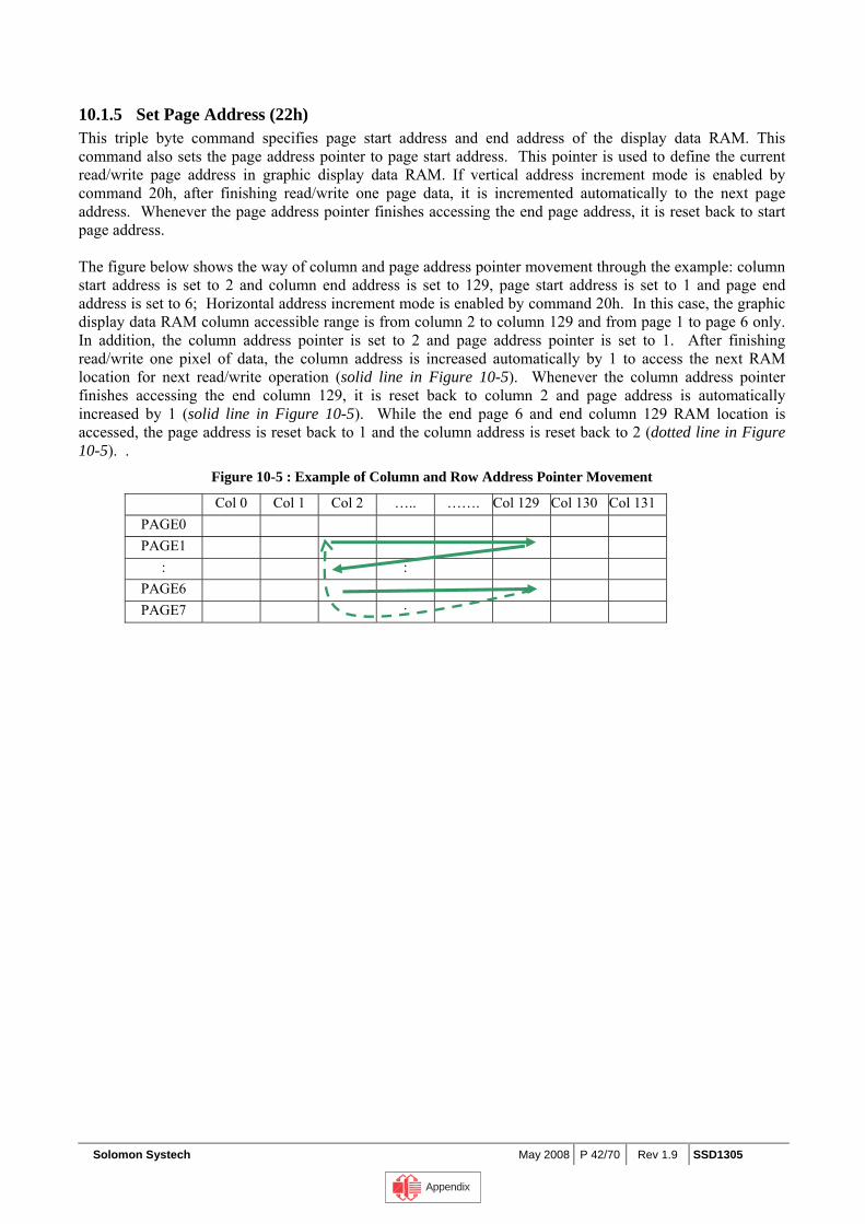
Solomon Systech May 2008 P 42/70 Rev 1.9 SSD1305
10.1.5 Set Page Address (22h) This triple byte command specifies page start address and end address of the display data RAM. This command also sets the page address pointer to page start address. This pointer is used to define the current read/write page address in graphic display data RAM. If vertical address increment mode is enabled by command 20h, after finishing read/write one page data, it is incremented automatically to the next page address. Whenever the page address pointer finishes accessing the end page address, it is reset back to start page address. The figure below shows the way of column and page address pointer movement through the example: column start address is set to 2 and column end address is set to 129, page start address is set to 1 and page end address is set to 6; Horizontal address increment mode is enabled by command 20h. In this case, the graphic display data RAM column accessible range is from column 2 to column 129 and from page 1 to page 6 only. In addition, the column address pointer is set to 2 and page address pointer is set to 1. After finishing read/write one pixel of data, the column address is increased automatically by 1 to access the next RAM location for next read/write operation (solid line in Figure 10-5). Whenever the column address pointer finishes accessing the end column 129, it is reset back to column 2 and page address is automatically increased by 1 (solid line in Figure 10-5). While the end page 6 and end column 129 RAM location is accessed, the page address is reset back to 1 and the column address is reset back to 2 (dotted line in Figure 10-5). .
Figure 10-5 : Example of Column and Row Address Pointer Movement
Col 0 Col 1 Col 2 ….. ……. Col 129 Col 130 Col 131 PAGE0 PAGE1
: : PAGE6 PAGE7 :
Appendix
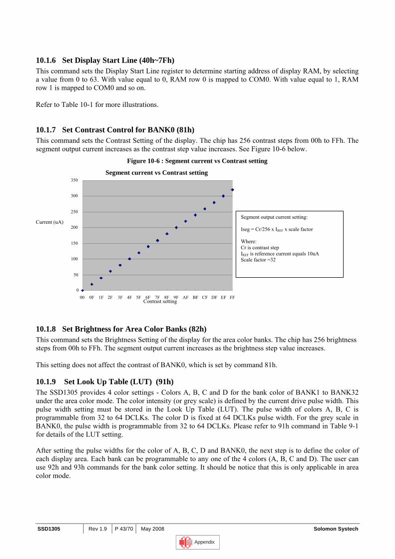
SSD1305 Rev 1.9 P 43/70 May 2008 Solomon Systech
10.1.6 Set Display Start Line (40h~7Fh) This command sets the Display Start Line register to determine starting address of display RAM, by selecting a value from 0 to 63. With value equal to 0, RAM row 0 is mapped to COM0. With value equal to 1, RAM row 1 is mapped to COM0 and so on. Refer to Table 10-1 for more illustrations.
10.1.7 Set Contrast Control for BANK0 (81h) This command sets the Contrast Setting of the display. The chip has 256 contrast steps from 00h to FFh. The segment output current increases as the contrast step value increases. See Figure 10-6 below.
Figure 10-6 : Segment current vs Contrast setting
Segment current vs Contrast setting
0
50
100
150
200
250
300
350
00 0F 1F 2F 3F 4F 5F 6F 7F 8F 9F AF BF CF DF EF FFContrast setting
Current (uA)
10.1.8 Set Brightness for Area Color Banks (82h) This command sets the Brightness Setting of the display for the area color banks. The chip has 256 brightness steps from 00h to FFh. The segment output current increases as the brightness step value increases. This setting does not affect the contrast of BANK0, which is set by command 81h.
10.1.9 Set Look Up Table (LUT) (91h) The SSD1305 provides 4 color settings - Colors A, B, C and D for the bank color of BANK1 to BANK32 under the area color mode. The color intensity (or grey scale) is defined by the current drive pulse width. This pulse width setting must be stored in the Look Up Table (LUT). The pulse width of colors A, B, C is programmable from 32 to 64 DCLKs. The color D is fixed at 64 DCLKs pulse width. For the grey scale in BANK0, the pulse width is programmable from 32 to 64 DCLKs. Please refer to 91h command in Table 9-1 for details of the LUT setting. After setting the pulse widths for the color of A, B, C, D and BANK0, the next step is to define the color of each display area. Each bank can be programmable to any one of the 4 colors (A, B, C and D). The user can use 92h and 93h commands for the bank color setting. It should be notice that this is only applicable in area color mode.
Segment output current setting: Iseg = Cr/256 x IREF x scale factor Where: Cr is contrast step IREF is reference current equals 10uA Scale factor =32
Appendix
Solomon Systech May 2008 P 44/70 Rev 1.9 SSD1305
10.1.10 Set Bank Color of BANK1 to BANK16 (PAGE0) (92h) This command maps the bank color (pulse width) of BANK1~BANK16 to any one of the 4 colors: A, B, C and D. For details of the setting, please refer to 92h command in Table 9-1.
10.1.11 Set Bank Color of BANK17 to BANK32 (PAGE0) (93h) This command maps the bank color (pulse width) of BANK17~BANK32 to any one of the 4 colors: A, B, C and D. For details of the setting, please refer to 93h command in Table 9-1.
10.1.12 Set Segment Re-map (A0h/A1h) This command changes the mapping between the display data column address and the segment driver. It allows flexibility in OLED module design. Please refer to Table 9-1. This command only affects subsequent data input. Data already stored in GDDRAM will have no changes.
10.1.13 Entire Display ON (A4h/A5h) A4h command enable display outputs according to the GDDRAM contents. If A5h command is issued, then by using A4h command, the display will resume to the GDDRAM contents. In other words, A4h command resumes the display from entire display “ON” stage. A5h command forces the entire display to be “ON”, regardless of the contents of the display data RAM.
10.1.14 Set Normal/Inverse Display (A6h/A7h) This command sets the display to be either normal or inverse. In normal display a RAM data of 1 indicates an “ON” pixel while in inverse display a RAM data of 0 indicates an “ON” pixel.
10.1.15 Set Multiplex Ratio (A8h) This command switches the default 63 multiplex mode to any multiplex ratio, ranging from 16 to 63. The output pads COM0~COM63 will be switched to the corresponding COM signal.
10.1.16 Reserved (AAh) This command is reserved.
10.1.17 Dim Mode setting (ABh) This command contains multiple bits to configure the contrast and brightness of color bank for the display in dim mode. The brightness setting of color bank can be set different to normal mode (AFh). The display can be set in dim mode through command ACh.
10.1.18 Master Configuration (ADh) This command selects the external VCC power supply by default. As external VCC power supply is selected, external VCC power should be connected to the VCC pin.
Appendix
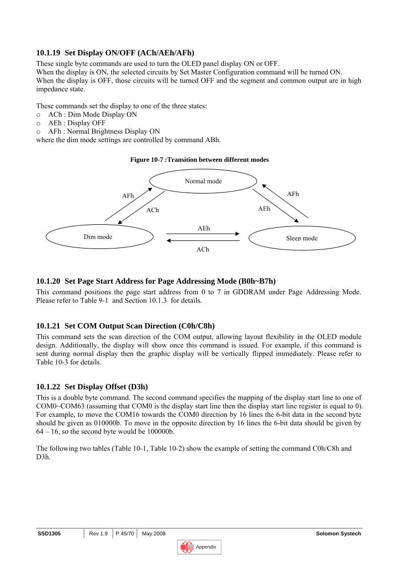
SSD1305 Rev 1.9 P 45/70 May 2008 Solomon Systech
10.1.19 Set Display ON/OFF (ACh/AEh/AFh) These single byte commands are used to turn the OLED panel display ON or OFF. When the display is ON, the selected circuits by Set Master Configuration command will be turned ON. When the display is OFF, those circuits will be turned OFF and the segment and common output are in high impedance state. These commands set the display to one of the three states: o ACh : Dim Mode Display ON o AEh : Display OFF o AFh : Normal Brightness Display ON where the dim mode settings are controlled by command ABh.
Figure 10-7 :Transition between different modes
10.1.20 Set Page Start Address for Page Addressing Mode (B0h~B7h) This command positions the page start address from 0 to 7 in GDDRAM under Page Addressing Mode. Please refer to Table 9-1 and Section 10.1.3 for details.
10.1.21 Set COM Output Scan Direction (C0h/C8h) This command sets the scan direction of the COM output, allowing layout flexibility in the OLED module design. Additionally, the display will show once this command is issued. For example, if this command is sent during normal display then the graphic display will be vertically flipped immediately. Please refer to Table 10-3 for details.
10.1.22 Set Display Offset (D3h) This is a double byte command. The second command specifies the mapping of the display start line to one of COM0~COM63 (assuming that COM0 is the display start line then the display start line register is equal to 0). For example, to move the COM16 towards the COM0 direction by 16 lines the 6-bit data in the second byte should be given as 010000b. To move in the opposite direction by 16 lines the 6-bit data should be given by 64 – 16, so the second byte would be 100000b. The following two tables (Table 10-1, Table 10-2) show the example of setting the command C0h/C8h and D3h.
Normal mode
Dim mode Sleep mode
AFh
AEhACh
AFh
ACh
AEh
Appendix
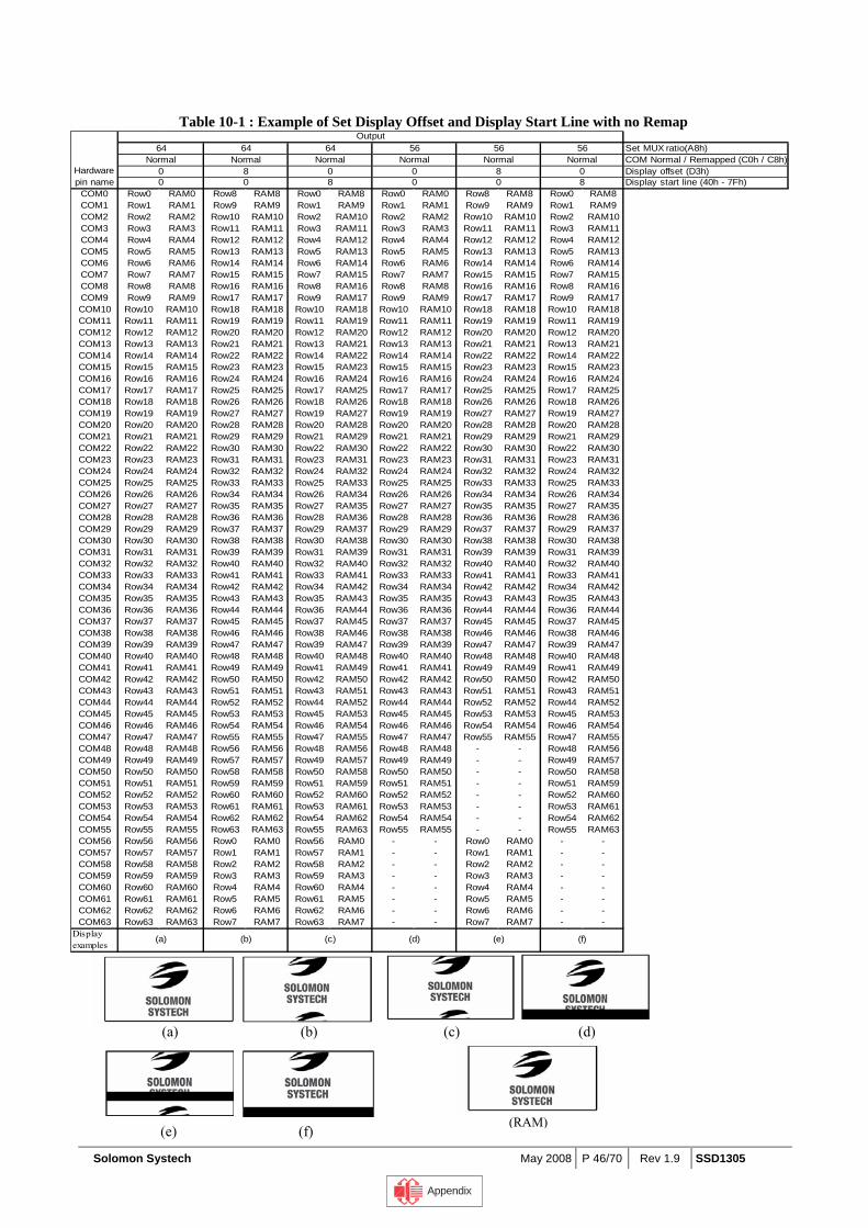
Solomon Systech May 2008 P 46/70 Rev 1.9 SSD1305
Table 10-1 : Example of Set Display Offset and Display Start Line with no Remap
(a) (b) (d)(c)
(e) (f) (RAM)
Set MUX ratio(A8h)COM Normal / Remapped (C0h / C8h)Display offset (D3h)Display start line (40h - 7Fh)
COM0 Row0 RAM0 Row8 RAM8 Row0 RAM8 Row0 RAM0 Row8 RAM8 Row0 RAM8COM1 Row1 RAM1 Row9 RAM9 Row1 RAM9 Row1 RAM1 Row9 RAM9 Row1 RAM9COM2 Row2 RAM2 Row10 RAM10 Row2 RAM10 Row2 RAM2 Row10 RAM10 Row2 RAM10COM3 Row3 RAM3 Row11 RAM11 Row3 RAM11 Row3 RAM3 Row11 RAM11 Row3 RAM11COM4 Row4 RAM4 Row12 RAM12 Row4 RAM12 Row4 RAM4 Row12 RAM12 Row4 RAM12COM5 Row5 RAM5 Row13 RAM13 Row5 RAM13 Row5 RAM5 Row13 RAM13 Row5 RAM13COM6 Row6 RAM6 Row14 RAM14 Row6 RAM14 Row6 RAM6 Row14 RAM14 Row6 RAM14COM7 Row7 RAM7 Row15 RAM15 Row7 RAM15 Row7 RAM7 Row15 RAM15 Row7 RAM15COM8 Row8 RAM8 Row16 RAM16 Row8 RAM16 Row8 RAM8 Row16 RAM16 Row8 RAM16COM9 Row9 RAM9 Row17 RAM17 Row9 RAM17 Row9 RAM9 Row17 RAM17 Row9 RAM17COM10 Row10 RAM10 Row18 RAM18 Row10 RAM18 Row10 RAM10 Row18 RAM18 Row10 RAM18COM11 Row11 RAM11 Row19 RAM19 Row11 RAM19 Row11 RAM11 Row19 RAM19 Row11 RAM19COM12 Row12 RAM12 Row20 RAM20 Row12 RAM20 Row12 RAM12 Row20 RAM20 Row12 RAM20COM13 Row13 RAM13 Row21 RAM21 Row13 RAM21 Row13 RAM13 Row21 RAM21 Row13 RAM21COM14 Row14 RAM14 Row22 RAM22 Row14 RAM22 Row14 RAM14 Row22 RAM22 Row14 RAM22COM15 Row15 RAM15 Row23 RAM23 Row15 RAM23 Row15 RAM15 Row23 RAM23 Row15 RAM23COM16 Row16 RAM16 Row24 RAM24 Row16 RAM24 Row16 RAM16 Row24 RAM24 Row16 RAM24COM17 Row17 RAM17 Row25 RAM25 Row17 RAM25 Row17 RAM17 Row25 RAM25 Row17 RAM25COM18 Row18 RAM18 Row26 RAM26 Row18 RAM26 Row18 RAM18 Row26 RAM26 Row18 RAM26COM19 Row19 RAM19 Row27 RAM27 Row19 RAM27 Row19 RAM19 Row27 RAM27 Row19 RAM27COM20 Row20 RAM20 Row28 RAM28 Row20 RAM28 Row20 RAM20 Row28 RAM28 Row20 RAM28COM21 Row21 RAM21 Row29 RAM29 Row21 RAM29 Row21 RAM21 Row29 RAM29 Row21 RAM29COM22 Row22 RAM22 Row30 RAM30 Row22 RAM30 Row22 RAM22 Row30 RAM30 Row22 RAM30COM23 Row23 RAM23 Row31 RAM31 Row23 RAM31 Row23 RAM23 Row31 RAM31 Row23 RAM31COM24 Row24 RAM24 Row32 RAM32 Row24 RAM32 Row24 RAM24 Row32 RAM32 Row24 RAM32COM25 Row25 RAM25 Row33 RAM33 Row25 RAM33 Row25 RAM25 Row33 RAM33 Row25 RAM33COM26 Row26 RAM26 Row34 RAM34 Row26 RAM34 Row26 RAM26 Row34 RAM34 Row26 RAM34COM27 Row27 RAM27 Row35 RAM35 Row27 RAM35 Row27 RAM27 Row35 RAM35 Row27 RAM35COM28 Row28 RAM28 Row36 RAM36 Row28 RAM36 Row28 RAM28 Row36 RAM36 Row28 RAM36COM29 Row29 RAM29 Row37 RAM37 Row29 RAM37 Row29 RAM29 Row37 RAM37 Row29 RAM37COM30 Row30 RAM30 Row38 RAM38 Row30 RAM38 Row30 RAM30 Row38 RAM38 Row30 RAM38COM31 Row31 RAM31 Row39 RAM39 Row31 RAM39 Row31 RAM31 Row39 RAM39 Row31 RAM39COM32 Row32 RAM32 Row40 RAM40 Row32 RAM40 Row32 RAM32 Row40 RAM40 Row32 RAM40COM33 Row33 RAM33 Row41 RAM41 Row33 RAM41 Row33 RAM33 Row41 RAM41 Row33 RAM41COM34 Row34 RAM34 Row42 RAM42 Row34 RAM42 Row34 RAM34 Row42 RAM42 Row34 RAM42COM35 Row35 RAM35 Row43 RAM43 Row35 RAM43 Row35 RAM35 Row43 RAM43 Row35 RAM43COM36 Row36 RAM36 Row44 RAM44 Row36 RAM44 Row36 RAM36 Row44 RAM44 Row36 RAM44COM37 Row37 RAM37 Row45 RAM45 Row37 RAM45 Row37 RAM37 Row45 RAM45 Row37 RAM45COM38 Row38 RAM38 Row46 RAM46 Row38 RAM46 Row38 RAM38 Row46 RAM46 Row38 RAM46COM39 Row39 RAM39 Row47 RAM47 Row39 RAM47 Row39 RAM39 Row47 RAM47 Row39 RAM47COM40 Row40 RAM40 Row48 RAM48 Row40 RAM48 Row40 RAM40 Row48 RAM48 Row40 RAM48COM41 Row41 RAM41 Row49 RAM49 Row41 RAM49 Row41 RAM41 Row49 RAM49 Row41 RAM49COM42 Row42 RAM42 Row50 RAM50 Row42 RAM50 Row42 RAM42 Row50 RAM50 Row42 RAM50COM43 Row43 RAM43 Row51 RAM51 Row43 RAM51 Row43 RAM43 Row51 RAM51 Row43 RAM51COM44 Row44 RAM44 Row52 RAM52 Row44 RAM52 Row44 RAM44 Row52 RAM52 Row44 RAM52COM45 Row45 RAM45 Row53 RAM53 Row45 RAM53 Row45 RAM45 Row53 RAM53 Row45 RAM53COM46 Row46 RAM46 Row54 RAM54 Row46 RAM54 Row46 RAM46 Row54 RAM54 Row46 RAM54COM47 Row47 RAM47 Row55 RAM55 Row47 RAM55 Row47 RAM47 Row55 RAM55 Row47 RAM55COM48 Row48 RAM48 Row56 RAM56 Row48 RAM56 Row48 RAM48 - - Row48 RAM56COM49 Row49 RAM49 Row57 RAM57 Row49 RAM57 Row49 RAM49 - - Row49 RAM57COM50 Row50 RAM50 Row58 RAM58 Row50 RAM58 Row50 RAM50 - - Row50 RAM58COM51 Row51 RAM51 Row59 RAM59 Row51 RAM59 Row51 RAM51 - - Row51 RAM59COM52 Row52 RAM52 Row60 RAM60 Row52 RAM60 Row52 RAM52 - - Row52 RAM60COM53 Row53 RAM53 Row61 RAM61 Row53 RAM61 Row53 RAM53 - - Row53 RAM61COM54 Row54 RAM54 Row62 RAM62 Row54 RAM62 Row54 RAM54 - - Row54 RAM62COM55 Row55 RAM55 Row63 RAM63 Row55 RAM63 Row55 RAM55 - - Row55 RAM63COM56 Row56 RAM56 Row0 RAM0 Row56 RAM0 - - Row0 RAM0 - -COM57 Row57 RAM57 Row1 RAM1 Row57 RAM1 - - Row1 RAM1 - -COM58 Row58 RAM58 Row2 RAM2 Row58 RAM2 - - Row2 RAM2 - -COM59 Row59 RAM59 Row3 RAM3 Row59 RAM3 - - Row3 RAM3 - -COM60 Row60 RAM60 Row4 RAM4 Row60 RAM4 - - Row4 RAM4 - -COM61 Row61 RAM61 Row5 RAM5 Row61 RAM5 - - Row5 RAM5 - -COM62 Row62 RAM62 Row6 RAM6 Row62 RAM6 - - Row6 RAM6 - -COM63 Row63 RAM63 Row7 RAM7 Row63 RAM7 - - Row7 RAM7 - -
Display examples
(e) (f)(a) (b) (c) (d)
0 8 00 0 8
56 56 56Normal Normal Normal
64Normal
08
Output
Hardware pin name 0
0Normal
64 64Normal
80
Appendix
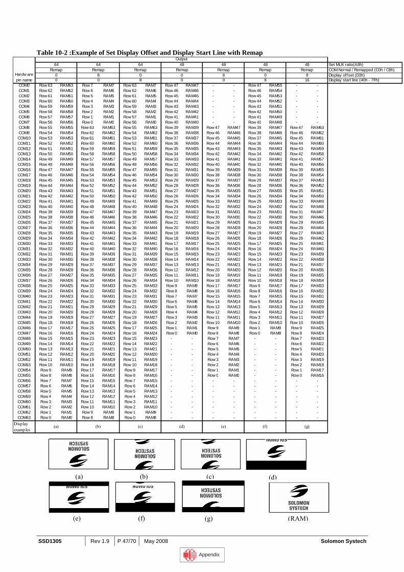
SSD1305 Rev 1.9 P 47/70 May 2008 Solomon Systech
Table 10-2 :Example of Set Display Offset and Display Start Line with Remap
(a) (b) (d)(c)
(e) (f) (g) (RAM)
Set MUX ratio(A8h)COM Normal / Remapped (C0h / C8h)Display offset (D3h)Display start line (40h - 7Fh)
COM0 Row 63 RAM63 Row 7 RAM7 Row 63 RAM7 Row 47 RAM47 - - Row 47 RAM55 - -COM1 Row 62 RAM62 Row 6 RAM6 Row 62 RAM6 Row 46 RAM46 - - Row 46 RAM54 - -COM2 Row 61 RAM61 Row 5 RAM5 Row 61 RAM5 Row 45 RAM45 - - Row 45 RAM53 - -COM3 Row 60 RAM60 Row 4 RAM4 Row 60 RAM4 Row 44 RAM44 - - Row 44 RAM52 - -COM4 Row 59 RAM59 Row 3 RAM3 Row 59 RAM3 Row 43 RAM43 - - Row 43 RAM51 - -COM5 Row 58 RAM58 Row 2 RAM2 Row 58 RAM2 Row 42 RAM42 - - Row 42 RAM50 - -COM6 Row 57 RAM57 Row 1 RAM1 Row 57 RAM1 Row 41 RAM41 - - Row 41 RAM49 - -COM7 Row 56 RAM56 Row 0 RAM0 Row 56 RAM0 Row 40 RAM40 - - Row 40 RAM48 - -COM8 Row 55 RAM55 Row 63 RAM63 Row 55 RAM63 Row 39 RAM39 Row 47 RAM47 Row 39 RAM47 Row 47 RAM63COM9 Row 54 RAM54 Row 62 RAM62 Row 54 RAM62 Row 38 RAM38 Row 46 RAM46 Row 38 RAM46 Row 46 RAM62COM10 Row 53 RAM53 Row 61 RAM61 Row 53 RAM61 Row 37 RAM37 Row 45 RAM45 Row 37 RAM45 Row 45 RAM61COM11 Row 52 RAM52 Row 60 RAM60 Row 52 RAM60 Row 36 RAM36 Row 44 RAM44 Row 36 RAM44 Row 44 RAM60COM12 Row 51 RAM51 Row 59 RAM59 Row 51 RAM59 Row 35 RAM35 Row 43 RAM43 Row 35 RAM43 Row 43 RAM59COM13 Row 50 RAM50 Row 58 RAM58 Row 50 RAM58 Row 34 RAM34 Row 42 RAM42 Row 34 RAM42 Row 42 RAM58COM14 Row 49 RAM49 Row 57 RAM57 Row 49 RAM57 Row 33 RAM33 Row 41 RAM41 Row 33 RAM41 Row 41 RAM57COM15 Row 48 RAM48 Row 56 RAM56 Row 48 RAM56 Row 32 RAM32 Row 40 RAM40 Row 32 RAM40 Row 40 RAM56COM16 Row 47 RAM47 Row 55 RAM55 Row 47 RAM55 Row 31 RAM31 Row 39 RAM39 Row 31 RAM39 Row 39 RAM55COM17 Row 46 RAM46 Row 54 RAM54 Row 46 RAM54 Row 30 RAM30 Row 38 RAM38 Row 30 RAM38 Row 38 RAM54COM18 Row 45 RAM45 Row 53 RAM53 Row 45 RAM53 Row 29 RAM29 Row 37 RAM37 Row 29 RAM37 Row 37 RAM53COM19 Row 44 RAM44 Row 52 RAM52 Row 44 RAM52 Row 28 RAM28 Row 36 RAM36 Row 28 RAM36 Row 36 RAM52COM20 Row 43 RAM43 Row 51 RAM51 Row 43 RAM51 Row 27 RAM27 Row 35 RAM35 Row 27 RAM35 Row 35 RAM51COM21 Row 42 RAM42 Row 50 RAM50 Row 42 RAM50 Row 26 RAM26 Row 34 RAM34 Row 26 RAM34 Row 34 RAM50COM22 Row 41 RAM41 Row 49 RAM49 Row 41 RAM49 Row 25 RAM25 Row 33 RAM33 Row 25 RAM33 Row 33 RAM49COM23 Row 40 RAM40 Row 48 RAM48 Row 40 RAM48 Row 24 RAM24 Row 32 RAM32 Row 24 RAM32 Row 32 RAM48COM24 Row 39 RAM39 Row 47 RAM47 Row 39 RAM47 Row 23 RAM23 Row 31 RAM31 Row 23 RAM31 Row 31 RAM47COM25 Row 38 RAM38 Row 46 RAM46 Row 38 RAM46 Row 22 RAM22 Row 30 RAM30 Row 22 RAM30 Row 30 RAM46COM26 Row 37 RAM37 Row 45 RAM45 Row 37 RAM45 Row 21 RAM21 Row 29 RAM29 Row 21 RAM29 Row 29 RAM45COM27 Row 36 RAM36 Row 44 RAM44 Row 36 RAM44 Row 20 RAM20 Row 28 RAM28 Row 20 RAM28 Row 28 RAM44COM28 Row 35 RAM35 Row 43 RAM43 Row 35 RAM43 Row 19 RAM19 Row 27 RAM27 Row 19 RAM27 Row 27 RAM43COM29 Row 34 RAM34 Row 42 RAM42 Row 34 RAM42 Row 18 RAM18 Row 26 RAM26 Row 18 RAM26 Row 26 RAM42COM30 Row 33 RAM33 Row 41 RAM41 Row 33 RAM41 Row 17 RAM17 Row 25 RAM25 Row 17 RAM25 Row 25 RAM41COM31 Row 32 RAM32 Row 40 RAM40 Row 32 RAM40 Row 16 RAM16 Row 24 RAM24 Row 16 RAM24 Row 24 RAM40COM32 Row 31 RAM31 Row 39 RAM39 Row 31 RAM39 Row 15 RAM15 Row 23 RAM23 Row 15 RAM23 Row 23 RAM39COM33 Row 30 RAM30 Row 38 RAM38 Row 30 RAM38 Row 14 RAM14 Row 22 RAM22 Row 14 RAM22 Row 22 RAM38COM34 Row 29 RAM29 Row 37 RAM37 Row 29 RAM37 Row 13 RAM13 Row 21 RAM21 Row 13 RAM21 Row 21 RAM37COM35 Row 28 RAM28 Row 36 RAM36 Row 28 RAM36 Row 12 RAM12 Row 20 RAM20 Row 12 RAM20 Row 20 RAM36COM36 Row 27 RAM27 Row 35 RAM35 Row 27 RAM35 Row 11 RAM11 Row 19 RAM19 Row 11 RAM19 Row 19 RAM35COM37 Row 26 RAM26 Row 34 RAM34 Row 26 RAM34 Row 10 RAM10 Row 18 RAM18 Row 10 RAM18 Row 18 RAM34COM38 Row 25 RAM25 Row 33 RAM33 Row 25 RAM33 Row 9 RAM9 Row 17 RAM17 Row 9 RAM17 Row 17 RAM33COM39 Row 24 RAM24 Row 32 RAM32 Row 24 RAM32 Row 8 RAM8 Row 16 RAM16 Row 8 RAM16 Row 16 RAM32COM40 Row 23 RAM23 Row 31 RAM31 Row 23 RAM31 Row 7 RAM7 Row 15 RAM15 Row 7 RAM15 Row 15 RAM31COM41 Row 22 RAM22 Row 30 RAM30 Row 22 RAM30 Row 6 RAM6 Row 14 RAM14 Row 6 RAM14 Row 14 RAM30COM42 Row 21 RAM21 Row 29 RAM29 Row 21 RAM29 Row 5 RAM5 Row 13 RAM13 Row 5 RAM13 Row 13 RAM29COM43 Row 20 RAM20 Row 28 RAM28 Row 20 RAM28 Row 4 RAM4 Row 12 RAM12 Row 4 RAM12 Row 12 RAM28COM44 Row 19 RAM19 Row 27 RAM27 Row 19 RAM27 Row 3 RAM3 Row 11 RAM11 Row 3 RAM11 Row 11 RAM27COM45 Row 18 RAM18 Row 26 RAM26 Row 18 RAM26 Row 2 RAM2 Row 10 RAM10 Row 2 RAM10 Row 10 RAM26COM46 Row 17 RAM17 Row 25 RAM25 Row 17 RAM25 Row 1 RAM1 Row 9 RAM9 Row 1 RAM9 Row 9 RAM25COM47 Row 16 RAM16 Row 24 RAM24 Row 16 RAM24 Row 0 RAM0 Row 8 RAM8 Row 0 RAM8 Row 8 RAM24COM48 Row 15 RAM15 Row 23 RAM23 Row 15 RAM23 - - Row 7 RAM7 - - Row 7 RAM23COM49 Row 14 RAM14 Row 22 RAM22 Row 14 RAM22 - - Row 6 RAM6 - - Row 6 RAM22COM50 Row 13 RAM13 Row 21 RAM21 Row 13 RAM21 - - Row 5 RAM5 - - Row 5 RAM21COM51 Row 12 RAM12 Row 20 RAM20 Row 12 RAM20 - - Row 4 RAM4 - - Row 4 RAM20COM52 Row 11 RAM11 Row 19 RAM19 Row 11 RAM19 - - Row 3 RAM3 - - Row 3 RAM19COM53 Row 10 RAM10 Row 18 RAM18 Row 10 RAM18 - - Row 2 RAM2 - - Row 2 RAM18COM54 Row 9 RAM9 Row 17 RAM17 Row 9 RAM17 - - Row 1 RAM1 - - Row 1 RAM17COM55 Row 8 RAM8 Row 16 RAM16 Row 8 RAM16 - - Row 0 RAM0 - - Row 0 RAM16COM56 Row 7 RAM7 Row 15 RAM15 Row 7 RAM15 - - - - - - - -COM57 Row 6 RAM6 Row 14 RAM14 Row 6 RAM14 - - - - - - - -COM58 Row 5 RAM5 Row 13 RAM13 Row 5 RAM13 - - - - - - - -COM59 Row 4 RAM4 Row 12 RAM12 Row 4 RAM12 - - - - - - - -COM60 Row 3 RAM3 Row 11 RAM11 Row 3 RAM11 - - - - - - - -COM61 Row 2 RAM2 Row 10 RAM10 Row 2 RAM10 - - - - - - - -COM62 Row 1 RAM1 Row 9 RAM9 Row 1 RAM9 - - - - - - - -COM63 Row 0 RAM0 Row 8 RAM8 Row 0 RAM8 - - - - - - - -
Display examples
(e) (f) (g)(a) (b) (c) (d)
Hardw are pin name
Output64 64 64
Remap Remap Remap0 8 00 0 8
48Remap
00
48 48Remap Remap
8 00 8
48Remap
816
Appendix
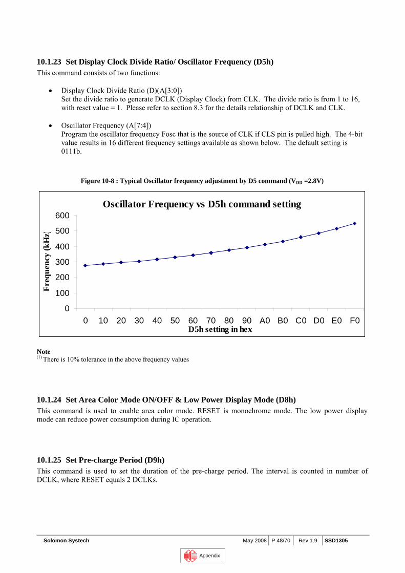
Solomon Systech May 2008 P 48/70 Rev 1.9 SSD1305
10.1.23 Set Display Clock Divide Ratio/ Oscillator Frequency (D5h) This command consists of two functions:
• Display Clock Divide Ratio (D)(A[3:0]) Set the divide ratio to generate DCLK (Display Clock) from CLK. The divide ratio is from 1 to 16, with reset value = 1. Please refer to section 8.3 for the details relationship of DCLK and CLK.
• Oscillator Frequency (A[7:4]) Program the oscillator frequency Fosc that is the source of CLK if CLS pin is pulled high. The 4-bit value results in 16 different frequency settings available as shown below. The default setting is 0111b.
Figure 10-8 : Typical Oscillator frequency adjustment by D5 command (VDD =2.8V)
Oscillator Frequency vs D5h command setting
0
100
200
300
400
500
600
0 10 20 30 40 50 60 70 80 90 A0 B0 C0 D0 E0 F0D5h setting in hex
Freq
uenc
y (k
Hz)
Note (1) There is 10% tolerance in the above frequency values
10.1.24 Set Area Color Mode ON/OFF & Low Power Display Mode (D8h) This command is used to enable area color mode. RESET is monochrome mode. The low power display mode can reduce power consumption during IC operation.
10.1.25 Set Pre-charge Period (D9h) This command is used to set the duration of the pre-charge period. The interval is counted in number of DCLK, where RESET equals 2 DCLKs.
Appendix
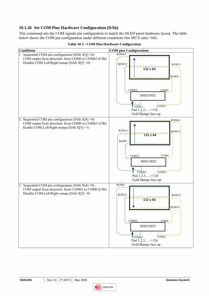
SSD1305 Rev 1.9 P 49/70 May 2008 Solomon Systech
10.1.26 Set COM Pins Hardware Configuration (DAh) This command sets the COM signals pin configuration to match the OLED panel hardware layout. The table below shows the COM pin configuration under different conditions (for MUX ratio =64):
Table 10-3 : COM Pins Hardware Configuration
Conditions COM pins Configurations 1 Sequential COM pin configuration (DAh X[4] =0)
COM output Scan direction: from COM0 to COM63 (C0h)Disable COM Left/Right remap (DAh X[5] =0)
2 Sequential COM pin configuration (DAh X[4] =0)
COM output Scan direction: from COM0 to COM63 (C0h)Enable COM Left/Right remap (DAh X[5] =1)
3 Sequential COM pin configuration (DAh X[4] =0)
COM output Scan direction: from COM63 to COM0 (C8h)Disable COM Left/Right remap (DAh X[5] =0)
132 x 64
ROW63
ROW32 ROW31
ROW0
Pad 1,2,3,…->126 Gold Bumps face up
SSD1305Z COM0
COM31
COM32
COM63
132 x 64 ROW32
ROW63
ROW0
ROW31
Pad 1,2,3,…->126 Gold Bumps face up
SSD1305Z
COM0
COM31 COM63
COM32
132 x 64
ROW0
ROW31 ROW32
ROW63
Pad 1,2,3,…->126 Gold Bumps face up
SSD1305Z COM0
COM31
COM32
COM63
Appendix
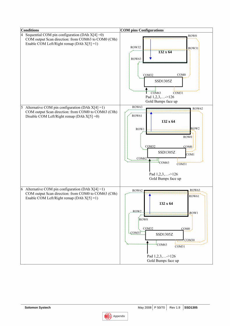
Solomon Systech May 2008 P 50/70 Rev 1.9 SSD1305
Conditions COM pins Configurations 4 Sequential COM pin configuration (DAh X[4] =0)
COM output Scan direction: from COM63 to COM0 (C8h)Enable COM Left/Right remap (DAh X[5] =1)
5 Alternative COM pin configuration (DAh X[4] =1)
COM output Scan direction: from COM0 to COM63 (C0h)Disable COM Left/Right remap (DAh X[5] =0)
6 Alternative COM pin configuration (DAh X[4] =1) COM output Scan direction: from COM0 to COM63 (C0h)Enable COM Left/Right remap (DAh X[5] =1)
132 x 64
ROW0
ROW62
ROW1
ROW63
Pad 1,2,3,…->126 Gold Bumps face up
SSD1305Z COM0
COM31
COM32
COM63
ROW61
COM62
ROW2
COM1
132 x 64
ROW2
ROW63
ROW0
ROW62
Pad 1,2,3,…->126 Gold Bumps face up
SSD1305Z COM0 COM32
COM63
ROW61
COM33
ROW1
COM31
COM30
132 x 64 ROW31
ROW0
ROW63
ROW32
Pad 1,2,3,…->126 Gold Bumps face up
SSD1305Z
COM0
COM31 COM63
COM32
Appendix
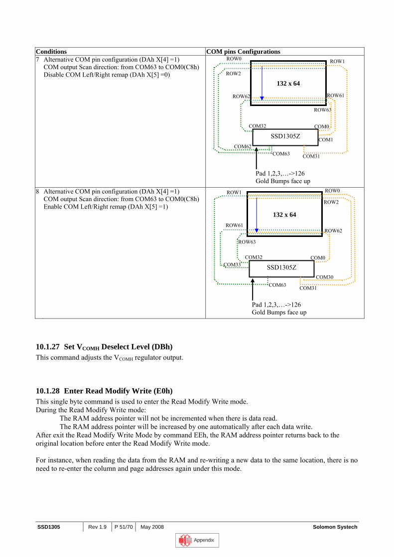
SSD1305 Rev 1.9 P 51/70 May 2008 Solomon Systech
Conditions COM pins Configurations 7 Alternative COM pin configuration (DAh X[4] =1)
COM output Scan direction: from COM63 to COM0(C8h) Disable COM Left/Right remap (DAh X[5] =0)
8 Alternative COM pin configuration (DAh X[4] =1)
COM output Scan direction: from COM63 to COM0(C8h) Enable COM Left/Right remap (DAh X[5] =1)
10.1.27 Set VCOMH Deselect Level (DBh) This command adjusts the VCOMH regulator output.
10.1.28 Enter Read Modify Write (E0h) This single byte command is used to enter the Read Modify Write mode. During the Read Modify Write mode:
The RAM address pointer will not be incremented when there is data read. The RAM address pointer will be increased by one automatically after each data write.
After exit the Read Modify Write Mode by command EEh, the RAM address pointer returns back to the original location before enter the Read Modify Write mode. For instance, when reading the data from the RAM and re-writing a new data to the same location, there is no need to re-enter the column and page addresses again under this mode.
132 x 64 ROW61
ROW0
ROW63
ROW1
Pad 1,2,3,…->126 Gold Bumps face up
SSD1305Z COM0 COM32
COM63
ROW2
COM33
ROW62
COM31
COM30
132 x 64
ROW63
ROW1
ROW62
ROW0
Pad 1,2,3,…->126 Gold Bumps face up
SSD1305Z COM0
COM31
COM32
COM63
ROW2
COM62
ROW61
COM1
Appendix
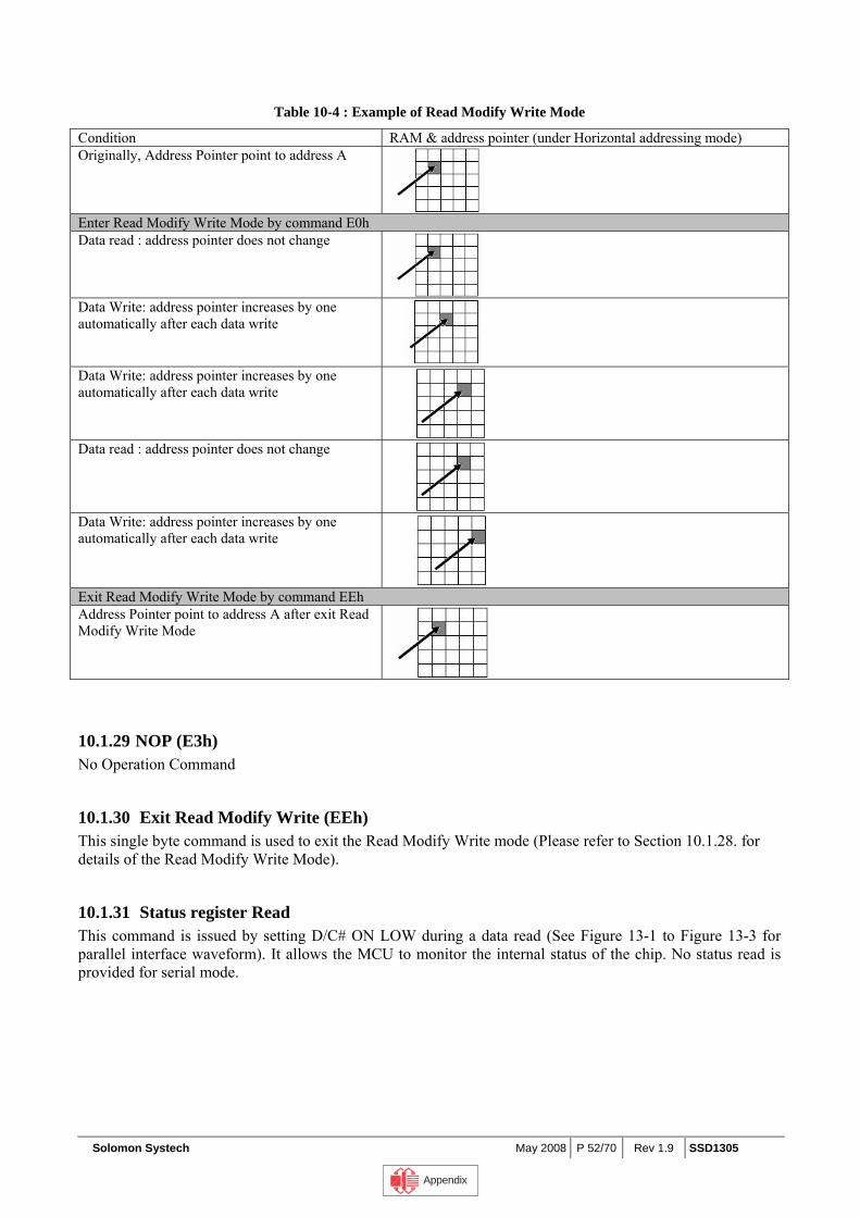
Solomon Systech May 2008 P 52/70 Rev 1.9 SSD1305
Table 10-4 : Example of Read Modify Write Mode
Condition RAM & address pointer (under Horizontal addressing mode) Originally, Address Pointer point to address A
Enter Read Modify Write Mode by command E0h Data read : address pointer does not change
Data Write: address pointer increases by one automatically after each data write
Data Write: address pointer increases by one automatically after each data write
Data read : address pointer does not change
Data Write: address pointer increases by one automatically after each data write
Exit Read Modify Write Mode by command EEh Address Pointer point to address A after exit Read Modify Write Mode
10.1.29 NOP (E3h) No Operation Command
10.1.30 Exit Read Modify Write (EEh) This single byte command is used to exit the Read Modify Write mode (Please refer to Section 10.1.28. for details of the Read Modify Write Mode).
10.1.31 Status register Read This command is issued by setting D/C# ON LOW during a data read (See Figure 13-1 to Figure 13-3 for parallel interface waveform). It allows the MCU to monitor the internal status of the chip. No status read is provided for serial mode.
Appendix
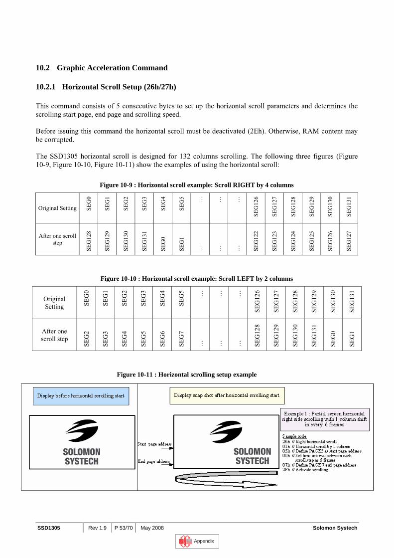
SSD1305 Rev 1.9 P 53/70 May 2008 Solomon Systech
10.2 Graphic Acceleration Command
10.2.1 Horizontal Scroll Setup (26h/27h) This command consists of 5 consecutive bytes to set up the horizontal scroll parameters and determines the scrolling start page, end page and scrolling speed. Before issuing this command the horizontal scroll must be deactivated (2Eh). Otherwise, RAM content may be corrupted. The SSD1305 horizontal scroll is designed for 132 columns scrolling. The following three figures (Figure 10-9, Figure 10-10, Figure 10-11) show the examples of using the horizontal scroll:
Figure 10-9 : Horizontal scroll example: Scroll RIGHT by 4 columns
Original Setting SEG
0
SEG
1
SEG
2
SEG
3
SEG
4
SEG
5 …
…
…
SEG
126
SEG
127
SEG
128
SEG
129
SEG
130
SEG
131
After one scroll step
SEG
128
SEG
129
SEG
130
SEG
131
SEG
0
SEG
1
…
…
…
SEG
122
SEG
123
SEG
124
SEG
125
SEG
126
SEG
127
Figure 10-10 : Horizontal scroll example: Scroll LEFT by 2 columns
Original Setting SE
G0
SEG
1
SEG
2
SEG
3
SEG
4
SEG
5 …
…
…
SEG
126
SEG
127
SEG
128
SEG
129
SEG
130
SEG
131
After one scroll step
SEG
2
SEG
3
SEG
4
SEG
5
SEG
6
SEG
7
…
…
…
SEG
128
SEG
129
SEG
130
SEG
131
SEG
0
SEG
1
Figure 10-11 : Horizontal scrolling setup example
Appendix
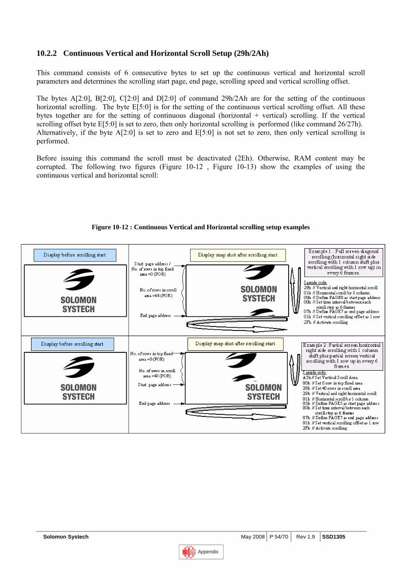
Solomon Systech May 2008 P 54/70 Rev 1.9 SSD1305
10.2.2 Continuous Vertical and Horizontal Scroll Setup (29h/2Ah) This command consists of 6 consecutive bytes to set up the continuous vertical and horizontal scroll parameters and determines the scrolling start page, end page, scrolling speed and vertical scrolling offset. The bytes A[2:0], B[2:0], C[2:0] and D[2:0] of command 29h/2Ah are for the setting of the continuous horizontal scrolling. The byte E[5:0] is for the setting of the continuous vertical scrolling offset. All these bytes together are for the setting of continuous diagonal (horizontal + vertical) scrolling. If the vertical scrolling offset byte E[5:0] is set to zero, then only horizontal scrolling is performed (like command 26/27h). Alternatively, if the byte A[2:0] is set to zero and E[5:0] is not set to zero, then only vertical scrolling is performed. Before issuing this command the scroll must be deactivated (2Eh). Otherwise, RAM content may be corrupted. The following two figures (Figure 10-12 , Figure 10-13) show the examples of using the continuous vertical and horizontal scroll:
Figure 10-12 : Continuous Vertical and Horizontal scrolling setup examples
Appendix
SSD1305 Rev 1.9 P 55/70 May 2008 Solomon Systech
Figure 10-13 : Continuous Vertical and Horizontal scrolling example: With setting in MUX ratio
As shown in Figure 10-13, the whole RAM content is displayed during scrolling regardless of the MUX ratio.
10.2.3 Deactivate Scroll (2Eh) This command stops the motion of scrolling. After sending 2Eh command to deactivate the scrolling action, the ram data needs to be rewritten.
10.2.4 Activate Scroll (2Fh) This command starts the motion of scrolling and should only be issued after the scroll setup parameters have been defined by the scrolling setup commands :26h/27h/29h/2Ah . The setting in the last scrolling setup command overwrites the setting in the previous scrolling setup commands. The following actions are prohibited after the scrolling is activated
1. RAM access (Data write or read) 2. Changing the horizontal scroll setup parameters
Appendix
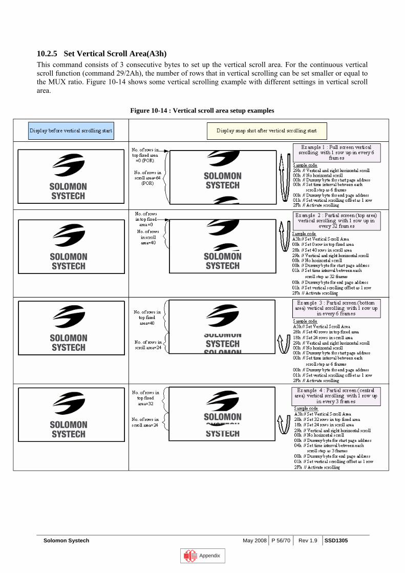
Solomon Systech May 2008 P 56/70 Rev 1.9 SSD1305
10.2.5 Set Vertical Scroll Area(A3h) This command consists of 3 consecutive bytes to set up the vertical scroll area. For the continuous vertical scroll function (command 29/2Ah), the number of rows that in vertical scrolling can be set smaller or equal to the MUX ratio. Figure 10-14 shows some vertical scrolling example with different settings in vertical scroll area.
Figure 10-14 : Vertical scroll area setup examples
Appendix
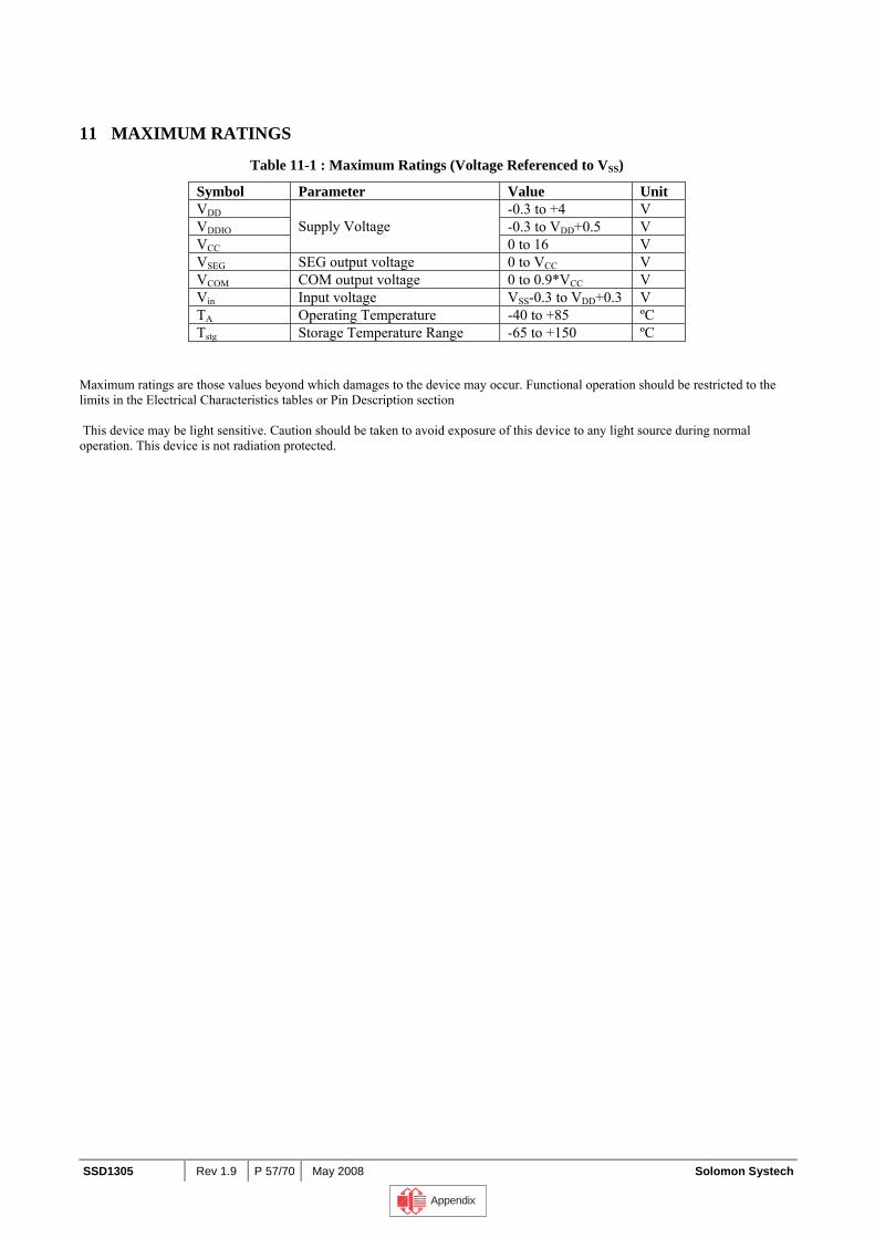
SSD1305 Rev 1.9 P 57/70 May 2008 Solomon Systech
11 MAXIMUM RATINGS
Table 11-1 : Maximum Ratings (Voltage Referenced to VSS)
Symbol Parameter Value Unit VDD -0.3 to +4 V VDDIO -0.3 to VDD+0.5 V VCC
Supply Voltage 0 to 16 V
VSEG SEG output voltage 0 to VCC V VCOM COM output voltage 0 to 0.9*VCC V Vin Input voltage VSS-0.3 to VDD+0.3 V TA Operating Temperature -40 to +85 ºC Tstg Storage Temperature Range -65 to +150 ºC
Maximum ratings are those values beyond which damages to the device may occur. Functional operation should be restricted to the limits in the Electrical Characteristics tables or Pin Description section This device may be light sensitive. Caution should be taken to avoid exposure of this device to any light source during normal operation. This device is not radiation protected.
Appendix
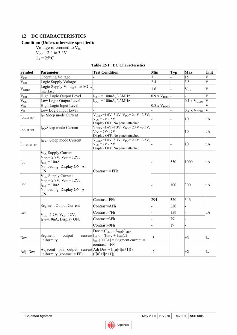
Solomon Systech May 2008 P 58/70 Rev 1.9 SSD1305
12 DC CHARACTERISTICS Condition (Unless otherwise specified):
Voltage referenced to VSS VDD = 2.4 to 3.5V TA = 25°C
Table 12-1 : DC Characteristics
Symbol Parameter Test Condition Min Typ Max UnitVCC Operating Voltage - 7 - 15 V VDD Logic Supply Voltage - 2.4 - 3.5 V
VDDIO Logic Supply Voltage for MCU interface - 1.6 - VDD V
VOH High Logic Output Level IOUT = 100uA, 3.3MHz 0.9 x VDDIO - - V VOL Low Logic Output Level IOUT = 100uA, 3.3MHz - - 0.1 x VDDIO V VIH High Logic Input Level - 0.8 x VDDIO - - V VIL Low Logic Input Level - - - 0.2 x VDDIO V ICC, SLEEP
ICC Sleep mode Current VDDIO =1.6V~3.3V, VDD = 2.4V ~3.5V, VCC = 7V~15V Display OFF, No panel attached
- - 10 uA
IDD, SLEEP
IDD Sleep mode Current VDDIO =1.6V~3.3V, VDD = 2.4V ~3.5V, VCC = 7V~15V Display OFF, No panel attached
- - 10 uA
IDDIO, SLEEP IDDIO Sleep mode Current VDDIO =1.6V~3.3V, VDD = 2.4V ~3.5V,
VCC = 7V~15V Display OFF, No panel attached
- - 10 uA
ICC
VCC Supply Current VDD = 2.7V, VCC = 12V, IREF = 10uA No loading, Display ON, All ON
- 550 1000 uA
IDD
VDD Supply Current VDD = 2.7V, VCC = 12V, IREF = 10uA No loading, Display ON, All ON
Contrast = FFh
- 100 300 uA
Contrast=FFh 294 320 346 Contrast=AFh - 220 - Contrast=7Fh - 159 - Contrast=3Fh - 79 -
ISEG
Segment Output Current VDD=2.7V, VCC=12V, IREF=10uA, Display ON.
Contrast=0Fh - 19 -
uA
Dev Segment output current uniformity
Dev = (ISEG – IMID)/IMID IMID = (IMAX + IMIN)/2 ISEG[0:131] = Segment current at contrast = FFh
-3 - +3 %
Adj. Dev Adjacent pin output current uniformity (contrast = FF)
Adj Dev = (I[n]-I[n+1]) / (I[n]+I[n+1]) -2 - +2 %
Appendix
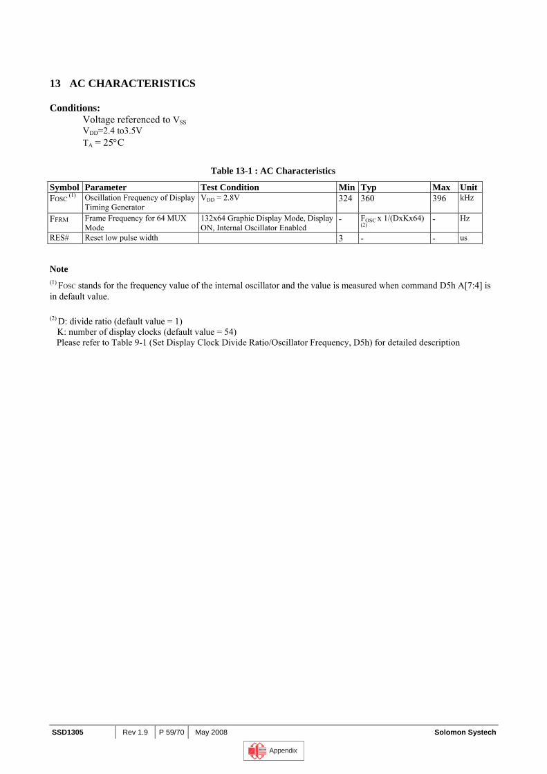
SSD1305 Rev 1.9 P 59/70 May 2008 Solomon Systech
13 AC CHARACTERISTICS Conditions:
Voltage referenced to VSS VDD=2.4 to3.5V TA = 25°C
Table 13-1 : AC Characteristics
Symbol Parameter Test Condition Min Typ Max UnitFOSC (1) Oscillation Frequency of Display
Timing Generator VDD = 2.8V
324 360 396 kHz
FFRM Frame Frequency for 64 MUX Mode
132x64 Graphic Display Mode, Display ON, Internal Oscillator Enabled
- FOSC x 1/(DxKx64) (2)
- Hz
RES# Reset low pulse width 3 - - us Note (1) FOSC stands for the frequency value of the internal oscillator and the value is measured when command D5h A[7:4] is in default value. (2) D: divide ratio (default value = 1) K: number of display clocks (default value = 54) Please refer to Table 9-1 (Set Display Clock Divide Ratio/Oscillator Frequency, D5h) for detailed description
Appendix
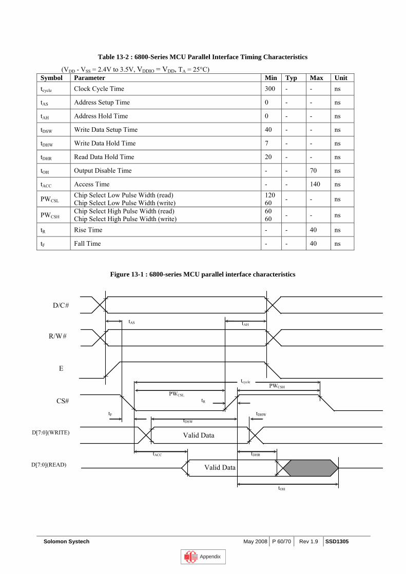
Solomon Systech May 2008 P 60/70 Rev 1.9 SSD1305
Table 13-2 : 6800-Series MCU Parallel Interface Timing Characteristics
(VDD - VSS = 2.4V to 3.5V, VDDIO = VDD, TA = 25°C) Symbol Parameter Min Typ Max Unit tcycle Clock Cycle Time 300 - - ns
tAS Address Setup Time 0 - - ns
tAH Address Hold Time 0 - - ns
tDSW Write Data Setup Time 40 - - ns
tDHW Write Data Hold Time 7 - - ns
tDHR Read Data Hold Time 20 - - ns
tOH Output Disable Time - - 70 ns
tACC Access Time - - 140 ns
PWCSL Chip Select Low Pulse Width (read) Chip Select Low Pulse Width (write)
120 60 - - ns
PWCSH Chip Select High Pulse Width (read) Chip Select High Pulse Width (write)
60 60 - - ns
tR Rise Time - - 40 ns
tF Fall Time - - 40 ns
Figure 13-1 : 6800-series MCU parallel interface characteristics
D[7:0](WRITE)
D[7:0](READ)
E
CS#
R/W#
PWCSLtR
tF tDHW
tOH
tACC tDHR
Valid Data
tDSW
Valid Data
tcyclePWCSH
tAHtAS
D/C#
Appendix
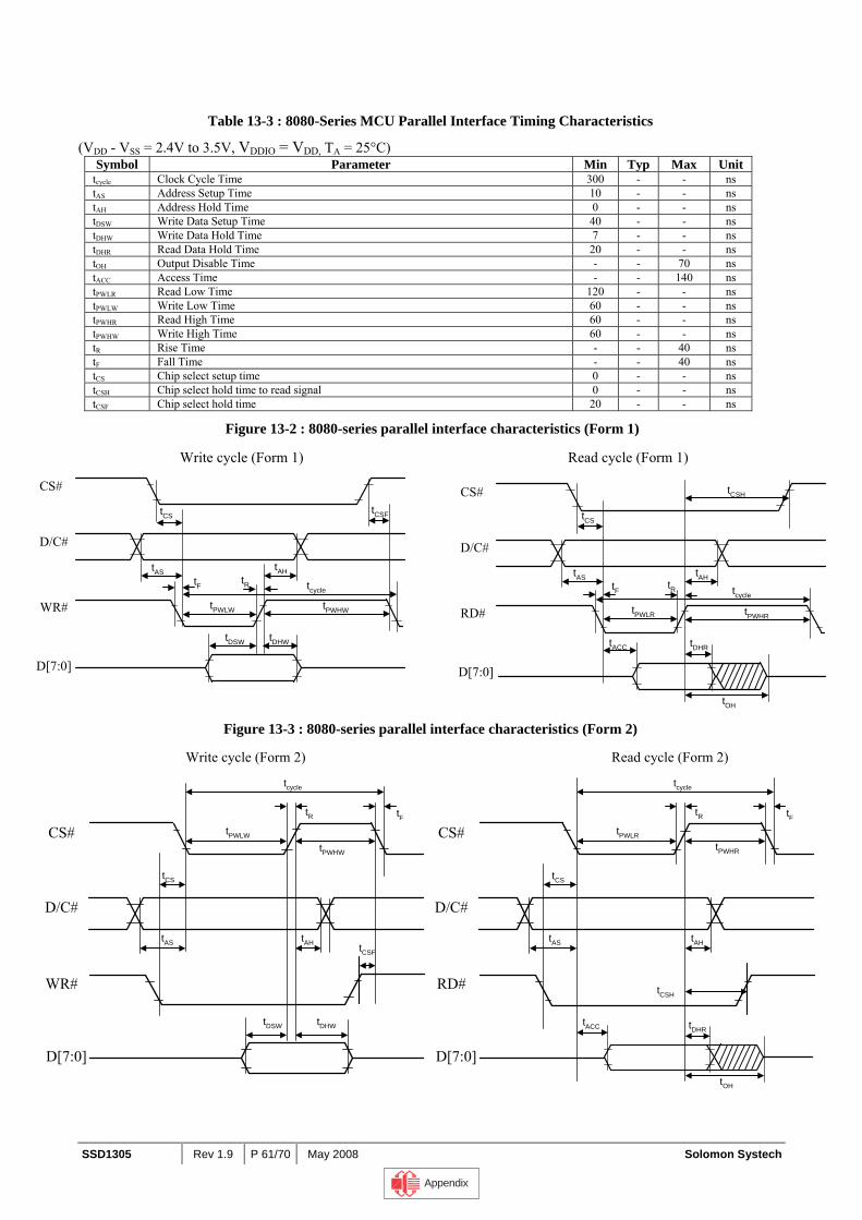
SSD1305 Rev 1.9 P 61/70 May 2008 Solomon Systech
Table 13-3 : 8080-Series MCU Parallel Interface Timing Characteristics
(VDD - VSS = 2.4V to 3.5V, VDDIO = VDD, TA = 25°C) Symbol Parameter Min Typ Max Unit
tcycle Clock Cycle Time 300 - - ns tAS Address Setup Time 10 - - ns tAH Address Hold Time 0 - - ns tDSW Write Data Setup Time 40 - - ns tDHW Write Data Hold Time 7 - - ns tDHR Read Data Hold Time 20 - - ns tOH Output Disable Time - - 70 ns tACC Access Time - - 140 ns tPWLR Read Low Time 120 - - ns tPWLW Write Low Time 60 - - ns tPWHR Read High Time 60 - - ns tPWHW Write High Time 60 - - ns tR Rise Time - - 40 ns tF Fall Time - - 40 ns tCS Chip select setup time 0 - - ns tCSH Chip select hold time to read signal 0 - - ns tCSF Chip select hold time 20 - - ns
Figure 13-2 : 8080-series parallel interface characteristics (Form 1)
WR#
D[7:0]
tAS
D/C#
CS#
tCS
tAH
tPWLW
tcycle
tDSW tDHW
tPWHW
tCSF
RD#
D[7:0]
tAS
D/C#
CS#
tCS
tAH
tPWLR
tcycle
tPWHR
tCSH
tACC tDHR
tOH
tF tR tF tR
Write cycle (Form 1) Read cycle (Form 1)
Figure 13-3 : 8080-series parallel interface characteristics (Form 2)
WR#
D[7:0]
D/C#
CS#
tcycle
tPWLW
tPWHW
tFtR
tCS
tAS tAH tCSF
tDSW tDHW
RD#
D[7:0]
D/C#
CS#
tcycle
tPWLR
tPWHR
tFtR
tCS
tAS tAH
tACC tDHR
tOH
tCSH
Write cycle (Form 2) Read cycle (Form 2)
Appendix
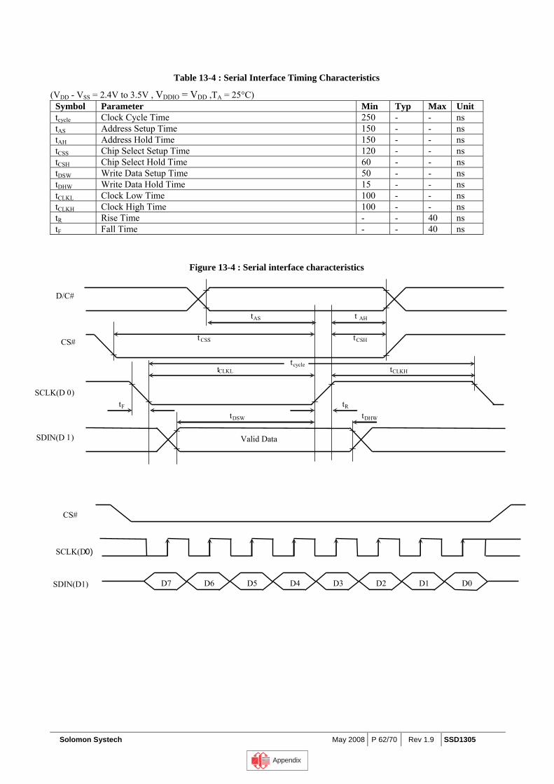
Solomon Systech May 2008 P 62/70 Rev 1.9 SSD1305
Table 13-4 : Serial Interface Timing Characteristics
(VDD - VSS = 2.4V to 3.5V , VDDIO = VDD ,TA = 25°C) Symbol Parameter Min Typ Max Unit tcycle Clock Cycle Time 250 - - ns tAS Address Setup Time 150 - - ns tAH Address Hold Time 150 - - ns tCSS Chip Select Setup Time 120 - - ns tCSH Chip Select Hold Time 60 - - ns tDSW Write Data Setup Time 50 - - ns tDHW Write Data Hold Time 15 - - ns tCLKL Clock Low Time 100 - - ns tCLKH Clock High Time 100 - - ns tR Rise Time - - 40 ns tF Fall Time - - 40 ns
Figure 13-4 : Serial interface characteristics
t AHtAS
D/C#
Valid Data
tDHW
t CLKL
tDSW
t CLKH tcycle
t CSS tCSH
t F tR
SDIN(D 1 )
CS#
SCLK(D 0 )
D7SDIN(D1)
CS#
SCLK(D 0 )
D6 D5 D4 D3 D2 D1 D0
Appendix
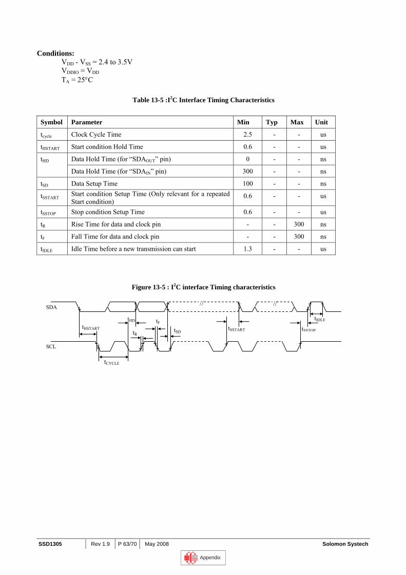
SSD1305 Rev 1.9 P 63/70 May 2008 Solomon Systech
Conditions: VDD - VSS = 2.4 to 3.5V VDDIO = VDD TA = 25°C
Table 13-5 :I2C Interface Timing Characteristics
Symbol Parameter Min Typ Max Unit
tcycle Clock Cycle Time 2.5 - - us
tHSTART Start condition Hold Time 0.6 - - us
Data Hold Time (for “SDAOUT” pin) 0 - - ns tHD
Data Hold Time (for “SDAIN” pin) 300 - - ns
tSD Data Setup Time 100 - - ns
tSSTART Start condition Setup Time (Only relevant for a repeated Start condition)
0.6 - - us
tSSTOP Stop condition Setup Time 0.6 - - us
tR Rise Time for data and clock pin - - 300 ns
tF Fall Time for data and clock pin - - 300 ns
tIDLE Idle Time before a new transmission can start 1.3 - - us
Figure 13-5 : I2C interface Timing characteristics
// //
SDA
SCL
tHSTART
tCYCLE
tHD
tR
tF tSD
tSSTART tSSTOP
tIDLE
Appendix
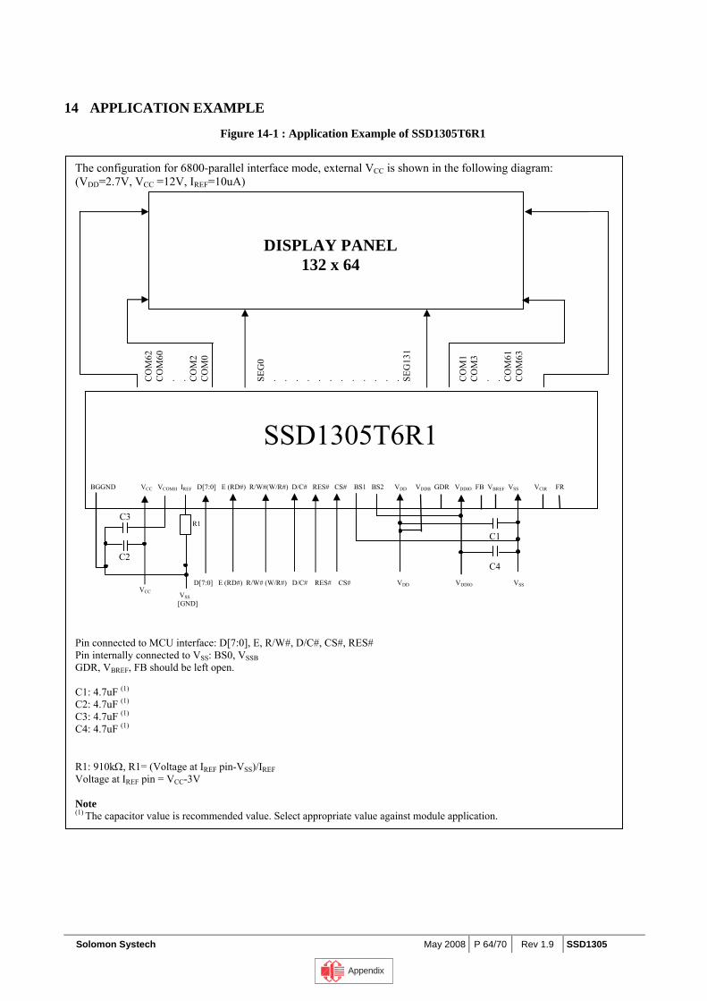
Solomon Systech May 2008 P 64/70 Rev 1.9 SSD1305
The configuration for 6800-parallel interface mode, external VCC is shown in the following diagram: (VDD=2.7V, VCC =12V, IREF=10uA) Pin connected to MCU interface: D[7:0], E, R/W#, D/C#, CS#, RES# Pin internally connected to VSS: BS0, VSSB GDR, VBREF, FB should be left open. C1: 4.7uF (1) C2: 4.7uF (1) C3: 4.7uF (1)
C4: 4.7uF (1)
R1: 910kΩ, R1= (Voltage at IREF pin-VSS)/IREF Voltage at IREF pin = VCC-3V Note (1) The capacitor value is recommended value. Select appropriate value against module application.
14 APPLICATION EXAMPLE
Figure 14-1 : Application Example of SSD1305T6R1
DISPLAY PANEL
132 x 64
CO
M62
C
OM
60
. . CO
M2
CO
M0
SEG
0 . . . . . . . . . . . . SE
G13
1 C
OM
1 C
OM
3 . . C
OM
61
CO
M63
SSD1305T6R1 BGGND VCC VCOMH IREF D[7:0] E (RD#) R/W#(W/R#) D/C# RES# CS# BS1 BS2 VDD VDDB GDR VDDIO FB VBREF VSS VCIR FR
R1
D[7:0] E (RD#) R/W# (W/R#) D/C# RES# CS# VDD VDDIO VSS
C1 C4
C2
VSS [GND]
C3
VCC
Appendix
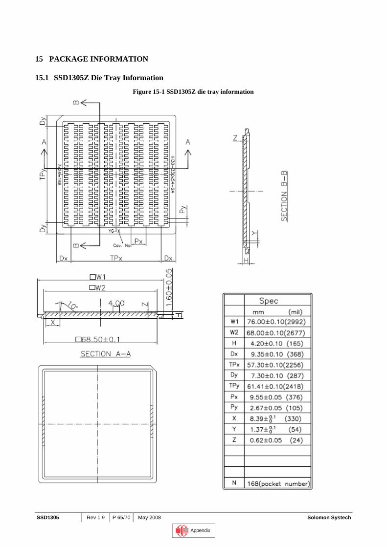
SSD1305 Rev 1.9 P 65/70 May 2008 Solomon Systech
15 PACKAGE INFORMATION
15.1 SSD1305Z Die Tray Information
Figure 15-1 SSD1305Z die tray information
Appendix
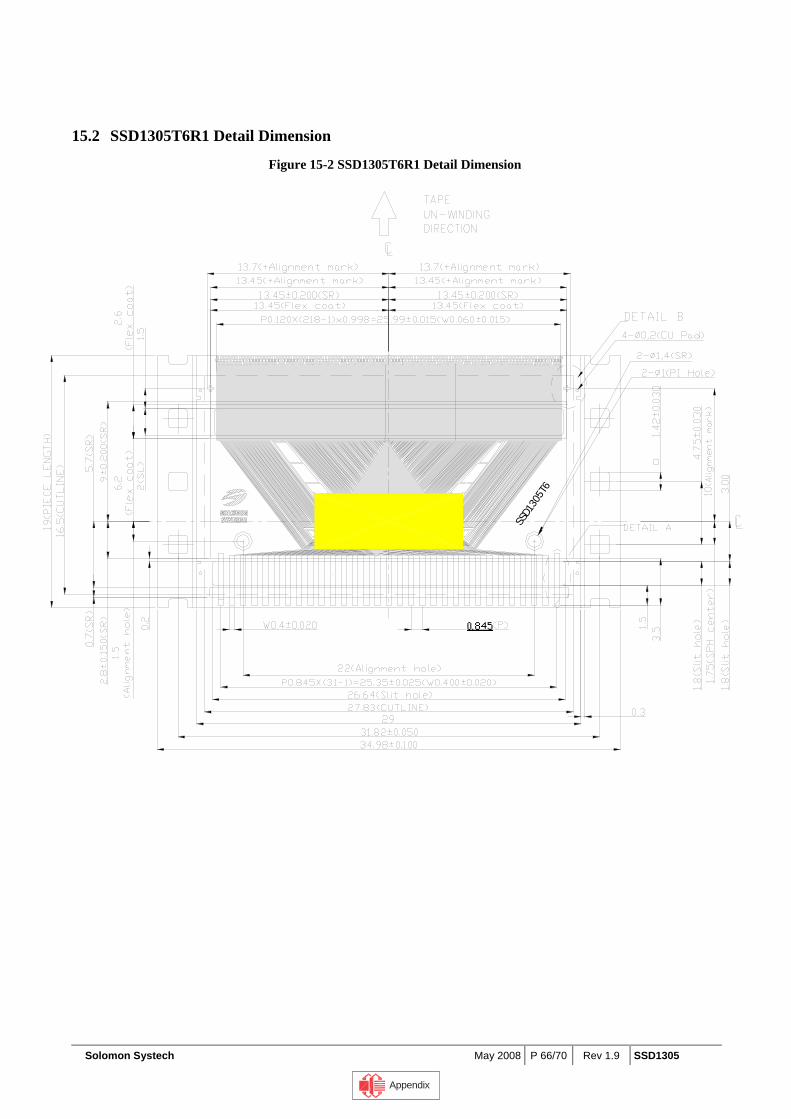
Solomon Systech May 2008 P 66/70 Rev 1.9 SSD1305
15.2 SSD1305T6R1 Detail Dimension
Figure 15-2 SSD1305T6R1 Detail Dimension
SSD1
305T
6
Appendix
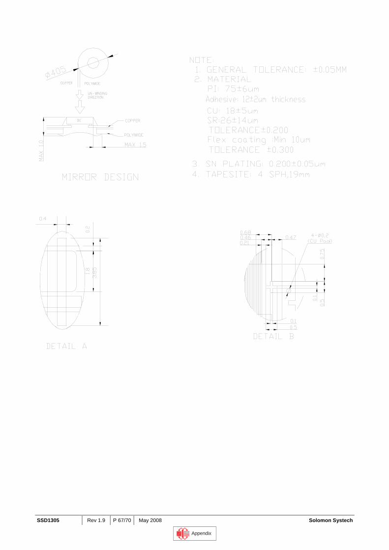
SSD1305 Rev 1.9 P 67/70 May 2008 Solomon Systech
Appendix
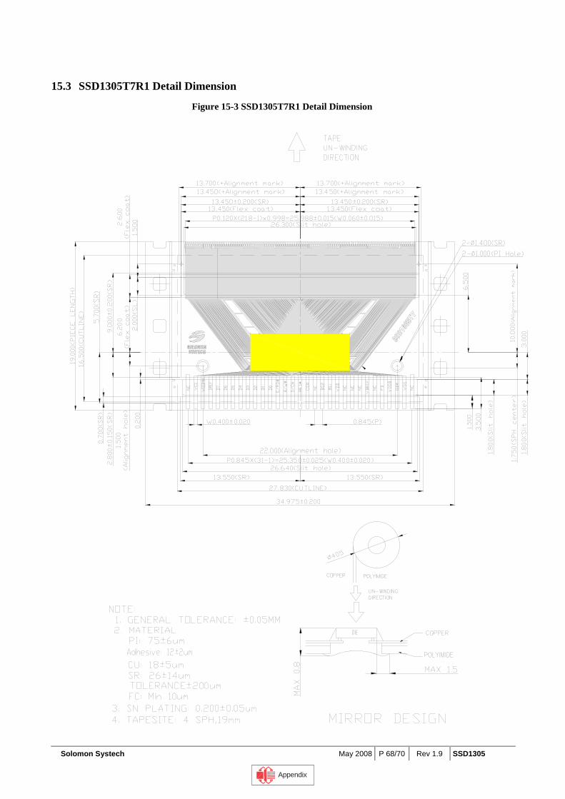
Solomon Systech May 2008 P 68/70 Rev 1.9 SSD1305
15.3 SSD1305T7R1 Detail Dimension
Figure 15-3 SSD1305T7R1 Detail Dimension
Appendix
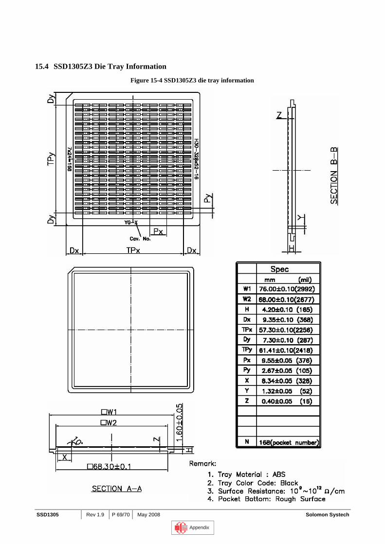
SSD1305 Rev 1.9 P 69/70 May 2008 Solomon Systech
15.4 SSD1305Z3 Die Tray Information
Figure 15-4 SSD1305Z3 die tray information
Appendix
Solomon Systech May 2008 P 70/70 Rev 1.9 SSD1305
Solomon Systech reserves the right to make changes without notice to any products herein. Solomon Systech makes no warranty, representation or guarantee regarding the suitability of its products for any particular purpose, nor does Solomon Systech assume any liability arising out of the application or use of any product or circuit, and specifically disclaims any, and all, liability, including without limitation consequential or incidental damages. “Typical” parameters can and do vary in different applications. All operating parameters, including “Typical” must be validated for each customer application by the customer’s technical experts. Solomon Systech does not con-vey any license under its patent rights nor the rights of others. Solomon Systech products are not designed, intended, or authorized for use as components in systems intended for surgical implant into the body, or other applications intended to support or sustain life, or for any other application in which the failure of the Solomon Systech product could create a situation where personal injury or death may occur. Should Buyer purchase or use Solomon Systech products for any such unintended or unauthorized application, Buyer shall indemnify and hold Solomon Systech and its offices, employees, subsidiaries, affiliates, and distributors harmless against all claims, costs, damages, and expenses, and reasonable attorney fees arising out of, directly or indirectly, any claim of personal injury or death associated with such unintended or unauthorized use, even if such claim alleges that Solomon Systech was negligent regarding the design or manufacture of the part.
All Solomon Systech Products complied with six (6) hazardous substances limitation requirement per European Union (EU) “Restriction of
Hazardous Substance (RoHS) Directive (2002/95/EC)” and China standard “电子信息产品污染控制标识要求 (SJ/T11364-2006)” with
control Marking Symbol .. Hazardous Substances test report is available upon requested.
http://www.solomon-systech.com
Appendix