Embed Size (px)
Citation preview

1
Graphene re-knits its holes
Recep Zan1,2, Quentin M. Ramasse3,*, Ursel Bangert2 and Konstantin S. Novoselov1
1School of Physics and Astronomy, The University of Manchester, Manchester, M13 9PL, United Kingdom
2School of Materials, The University of Manchester, Manchester, M13 9PL, United Kingdom
3SuperSTEM Laboratory, STFC Daresbury Campus, Daresbury WA4 4AD, United Kingdom
*To whom correspondence should be addressed: [email protected]
Abstract. Nano-holes, etched under an electron beam at room temperature in single-
layer graphene sheets as a result of their interaction with metal impurities, are shown to
heal spontaneously by filling up with either non-hexagon, graphene-like, or perfect hexagon
2D structures. Scanning transmission electron microscopy was employed to capture the
healing process and study atom-by-atom the re-grown structure. A combination of these
nano-scale etching and re-knitting processes could lead to new graphene tailoring
approaches.
Keywords. Graphene, Scanning Transmission Electron Microscopy, 2D materials
etching, self-healing.
TOC Graphic.

2
The development of graphene devices has entered a new era: graphene is rapidly moving
from the laboratory to the factory floor with an increasing effort directed towards achieving
devices that employ suspended membranes as well as graphene of defined geometries, e.g.,
nano-ribbons and quantum dots, because of their predicted novel, exceptional electronic
properties.1,2 As a result, the interfaces between graphene and other components of the
devices such as metal contacts are under intense scrutiny. We have recently shown that in
the presence of metals graphene can be etched on the nano-scale3,4 under exposure to an
electron probe following a sequence of point defect reactions, a process different from
previous attempts at graphene etching. In earlier studies, graphene and graphite were
etched or tailored in a gas environment (hydrogen or oxygen) at high temperatures.5-8 In
particular, the interaction of metals with the graphene surface in such extreme conditions
was shown both experimentally8 and theoretically9 to provide an efficient means of
controlling the etching process and effectively sculpt graphene/graphite nanostructures. A
recent review of these techniques was for instance compiled by Biró and Lambin.8
Additionally, a number of papers have previously discussed defects in graphene, either
following experimental transmission electron microscopy (TEM) studies,10-16 where defects
were introduced by the electron beam, or by simulations based on Density Functional
Theory (DFT) calculations.17-24 Defects studies in all those papers are based on reconstruction
of the graphene lattice as a result of knock-on of carbon atoms from the graphene lattice
(mono- and multi- vacancy) or/and as a result of bond rotations, e.g., the formation of
Stone-Wales (55-77) and 8-ring defects. Dynamics, stability and favourable arrangements of
the reconstructed lattice, with the occurrence of larger vacancy aggregates and holes, as
well as edge reconstructions thereof, are further aspects of those studies. Furthermore, new
structures with long range order, such as haeckelites18 consisting of 5-, 6- and 7-member
rings, or pentaheptides17 incorporating 5- and 7-member rings, have been proposed as result
of theoretical calculations. Here we report the first observations of reconstruction, i.e. the
mending and filling of many-vacancy holes (over 100 vacancies) in graphene, in an electron
microscope. We show that provided a reservoir of loose carbon atoms is readily available
nearby, holes in graphene can be re-filled with either non-hexagonal near-amorphous or
perfectly hexagonal 2-dimensional structures.

3
To study atomic arrangements we employ high angle annular dark field (HAADF) imaging in a
Nion UltraSTEM100TM aberration-corrected scanning transmission electron microscope
(STEM). The microscope was operated in 'Gentle STEM' conditions25 at 60 keV primary beam
energy to prevent knock-on damage to the graphene sheets, even after long intervals of
repeated scanning of small areas of a few square nanometers. The ultra-high-vacuum (UHV)
design of this instrument allows clean imaging conditions with pressures below 5x10⁻⁹ Torr
near the sample. The beam was set up to a convergence semi-angle of 30 mrad with an
estimated beam current of 45 pA. In these operating conditions the estimated probe size is
1.1 Å, providing the perfect tool for atom-by-atom chemical analysis26. These experimental
conditions (scanning probe, low primary beam energy, high vacuum conditions) are
significantly different from other studies of the dynamics of defects and edges in graphene,
which employ higher beam energies and are typically carried out in much poorer vacuum
conditions.12,27,28 Samples were obtained by transfer of graphene membranes grown by CVD
on copper substrates29 to TEM grids. Two different metals were deposited by electron beam
(Pd) and thermal (Ni) evaporation. Although there is no damage inferred to pristine
graphene with a 60 keV electron beam, we have recently demonstrated3,4 that in the
presence of transition-metal or silicon atoms, hole formation does occurs under the e-beam.
It is believed that the process occurs due to metal-catalysed dissociation of C-C bonds, which
leads to point defect formation. The role of the electron beam in this is mainly to mobilise
the metal atoms on graphene, and not to initiate the hole formation in the first place, i.e., by
carbon atom displacement. The beam may also act as a local heat source and thus help
overcome the defect formation energy barrier.4 This process is however different from high-
temperature TEM observations of graphene using a dedicated hot-stage holder, during
which amorphous contaminations layers were shown to either be removed totally,30 thus
cleaning the graphene, or be transformed into crystalline patches.31
Here, the resulting defects are enlarged in the presence of further metal atoms, which have
migrated under the electron beam to the edge of the incurred hole, upon which the process
repeats itself. The nature of the intentionally-deposited metal impurities was confirmed by
single-atom sensitive electron energy loss spectroscopy (EELS).4 When the reservoir of metal
atoms is exhausted, the process stops and the hole remains of almost the same size,

4
although the edges undergo repeated reconstruction in consecutive scans. If metal
impurities are not present and, at the same time, carbon atom supply is warranted, e.g.
through near-by hydrocarbon contamination attracted towards the hole by the scanning
probe, ‘filling’ occurs and the hole mends itself by non-hexagon arrangements. However, if
no hydrocarbon contamination is present, healing can occur via reconstruction of the
perfect graphene hexagon structure. The following Z-contrast images depict the hole
evolution and two filling scenarios, by non-hexagon and by hexagon structures, in freely
suspended graphene films where heavier foreign atoms are present either as residual
impurities or as a consequence of metal evaporation.
The deposition of metal atoms on CVD-grown graphene results in the formation of nm-sized
metal clusters sitting preferentially on patches of C-based surface contamination, ubiquitous
in suspended graphene membranes.32 Pd atoms, dislodged from a nearby Pd cluster by the
electron beam and 'dragged' across the sample until they settle in a new stable position as
the beam is being scanned, can be seen in fig. 1a to decorate a hole in graphene. Newly
arriving Pd atoms lead to hole expansion (fig 1b), whereas in the absence of metal atoms the
hole formation slows down and edge reconstruction takes place under the electron beam
(fig. 1c). Furthermore, figure 1 shows that the hole is bordered by hydrocarbon
contamination, which constitutes the carbon reservoir for the hole healing described below.
Figure 1. Atomic resolution HAADF images (raw data) from consecutive scans of suspended
graphene, showing a) an etched hole decorated with Pd atoms; b) the enlargement of the
hole following further supply of Pd atoms; c) the stabilization of the hole size in the absence
of Pd atoms at the edge.
5
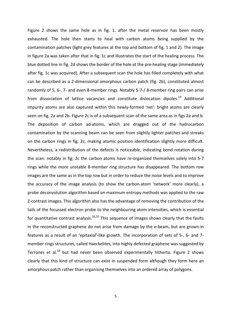
Figure 2 shows the same hole as in fig. 1. after the metal reservoir has been mostly
exhausted. The hole then starts to heal with carbon atoms being supplied by the
contamination patches (light grey features at the top and bottom of fig. 1 and 2). The image
in figure 2a was taken after that in fig. 1c and illustrates the start of the healing process. The
blue dotted line in fig. 2d shows the border of the hole at the pre-healing stage (immediately
after fig. 1c was acquired). After a subsequent scan the hole has filled completely with what
can be described as a 2-dimensional amorphous carbon patch (fig. 2b), constituted almost
randomly of 5, 6-, 7- and even 8-member rings. Notably 5-7-/ 8-member ring pairs can arise
from dissociation of lattice vacancies and constitute dislocation dipoles.19 Additional
impurity atoms are also captured within this newly-formed 'net': bright atoms are clearly
seen on fig. 2a and 2b. Figure 2c is of a subsequent scan of the same area as in figs 2a and b.
The deposition of carbon ad-atoms, which are dragged out of the hydrocarbon
contamination by the scanning beam can be seen from slightly lighter patches and streaks
on the carbon rings in fig. 2c, making atomic position identification slightly more difficult.
Nevertheless, a redistribution of the defects is noticeable, indicating bond rotation during
the scan: notably in fig. 2c the carbon atoms have re-organized themselves solely into 5-7
rings while the more unstable 8-member ring structure has disappeared. The bottom row
images are the same as in the top row but in order to reduce the noise levels and to improve
the accuracy of the image analysis (to show the carbon-atom 'network' more clearly), a
probe deconvolution algorithm based on maximum entropy methods was applied to the raw
Z-contrast images. This algorithm also has the advantage of removing the contribution of the
tails of the focussed electron probe to the neighbouring atom intensities, which is essential
for quantitative contrast analysis.26,33 This sequence of images shows clearly that the faults
in the reconstructed graphene do not arise from damage by the e-beam, but are grown-in
features as a result of an ‘epitaxial’-like growth. The incorporation of sets of 5-, 6- and 7-
member rings structures, called Haeckelites, into highly defected graphene was suggested by
Terrones et al.18 but had never been observed experimentally hitherto. Figure 2 shows
clearly that this kind of structure can exist in suspended form although they form here an
amorphous patch rather than organising themselves into an ordered array of polygons.

6
Figure 2. Atomic resolution Z-contrast images illustrating the hole filling process in
suspended graphene. a) a hole created at the border of hydrocarbon contamination b)
complete reconstruction with incorporation of 5-7 rings and two 5-8 rings, and c)
redistribution of defects in the ‘mended’ region, by 5-7 rings. Images d-f are processed
versions of a-c. A maximum entropy deconvolution algorithm was used and the contrast was
optimised to visualise the carbon atoms. The carbon atom positions are highlighted by light
green dots and polygons numbered according to the number of atoms in the rings.
Such 2-dimensional near-amorphous carbon layers can also grow 'epitaxially’ on graphene,
as illustrated on figure 3. After long observations of the same area of single layer graphene
(more than 40 minutes of observation in this case) some contamination can occasionally
'creep in' and cover the graphene sheet. The circled region on figure 3a is a single additional
carbon layer (as can be clearly deduced from the contrast in the image), which has formed
on top of the clean, underlying (dark) graphene patch after repeated scanning. The presence
of a Moiré pattern indicates that this additional layer has a similar structure to the
underlying graphene, but the patter is highly irregular and interrupted (as highlighted by the
arrows), unlike the patterns observed in pure Bernal-stacked graphene.34

7
Figure 3. Atomic resolution HAADF image (raw data) obtained after repeated scanning of the
same area; the circled area is an additional one-atom-thick carbon layer that has grown
‘epitaxially’ as a result of carbon atom supply from the hydrocarbon contamination
surrounding the pristine graphene patch. The Moiré pattern, however, is non-regular
(arrow), indicating the existence of random defected carbon ring networks in the newly-
grown layer as well as in the already existing contamination.
The newly-grown layer must therefore be heavily faulted. It likely contains a high density of
5- and 7-member rings, similar to the ‘re-knitted’ layer in fig 2b. This can again be
interpreted as an amorphous 2-dimensional layer with some degree of short-range
graphene-like order. The re-grown structures in figs. 2 and 3 provide a remarkable glimpse
into the atomic arrangements of amorphous carbon structures; they show the precise
atomic arrangements of a 2-D amorphous carbon material.14 By close inspection of atomic
resolution Z-contrast images of graphene films it can then be concluded that a large fraction
of the ubiquitous contamination (such as the lighter patches in fig. 3b) where material
deposited on graphene sits preferentially, consists of stacks of these amorphous mono-layer
carbon films.
By contrast, when a small hole is created away from the hydrocarbon contamination, the
self-healing mechanism appears to lead to the formation of perfect hexagons. Two holes are
apparent in fig. 4a, both created as a result of Ni-atom mediated graphene etching. The
small hole was created when Ni atoms from the edge of the larger hole, which had formed
earlier, were dislodged by the electron beam and 'dragged' onto a clean patch of graphene

8
where the etching was initiated, through the e-beam scanning motion. In subsequent scans,
after cessation of the migration of metal atoms to its edges, the small hole is observed to fill
up with perfect carbon hexagons (fig. 4b). This 're-knitting' process happened within a much
shorter time span (less than 10 seconds: two consecutive scans) compared to the previous
case (figs. 1&2). Impurity atoms are again trapped within the newly formed lattice, such as
the brighter atom indicated in fig. 4b by an arrow. After the contribution of the electron
probe 'tails' to the raw HAADF images has been removed (using for instance a maximum-
entropy-based probe deconvolution algorithm33), a careful comparison of atomic intensities
vs. atomic number Z with the model value of Z1.7 for HAADF imaging (in our experimental
conditions) can enable the chemical identification of these impurities.26 Figure 4c shows a
histogram of the frequency of occurrence of atoms versus their HAADF intensity in the
vicinity of the bright atom in Fig. 4b, obtained from the deconvoluted image in the inset in
fig. 4c. The positions of the intensity maxima are in the ratio of 1:1.66, which is close to the
Z1.7 ratios for Z = 6 (C) and Z = 8 (O), of 1:1.63. Although there is only one such impurity in
this image (and the statistics are therefore low) this is a good indication that the brighter
atom is likely oxygen.
Figure 4. Atomic resolution HAADF images (raw data) from subsequent scans of suspended
graphene, showing a) two holes as result of Ni-mediated etching, b) complete reconstruction
of small hole with perfect hexagon graphene structure. c) histogram of the atom intensities,
in the vicinity of the brighter atom: the analysis was carried out after processing image 4b
with a probe deconvolution algorithm (inset).
The size of the hole to fill is an obvious difference with the previous case and may explain
the formation of perfect hexagons: arguably, defects are less likely to form across such a
short growth distance. Moreover, the larger distance from the contamination reservoir and

9
the proximity to a much larger perforation in the graphene sheet may also play a role. Edges
in graphene are known to be more unstable even at low voltages12,15: atoms ejected from
the edge of this larger neighbouring hole may have been captured during the re-knitting
while the long edge may have reconfigured to accommodate the newly formed material into
the usual, energetically favourable honeycomb pattern. Additionally, using a low primary
beam energy (60 keV), clean vacuum conditions (<5x10⁻⁹ Torr) to reduce the ionization
damage probability, and a scanning probe, can help explaining our observations of hole-
filling, which contrast with previous reports of hole-expansion at 80 keV with a stationary
beam.12,28
In conclusion, etching of graphene occurs in the presence of metals; when the metal atom
supply ceases graphene reconstructs its holes by forming perfect hexagonal or polygonal, i.e.
5-, 6-, 7- and 8-member ring structures, which can exist either in suspended form or grow
'epitaxially' on top of clean graphene. Carbon atoms knocked out from neighbouring edges,
or supplied by nearby hydrocarbon contamination patches, are incorporated into the holes
in a remarkable re-knitting process. This observation of self-healing of graphene might open
up possibilities for the use of e-beam techniques in tailoring graphene in a ‘bottom-up’
fashion via nano-scale-controlled etching and epitaxial growth from sheet edges.
References
1. Geim, A. K.; Novoselov, K. S. Nat Mater 2007, 6, (3), 183-191.
2. Ponomarenko, L. A.; Geim, A. K.; Zhukov, A. A.; Jalil, R.; Morozov, S. V.; Novoselov, K. S.;
Grigorieva, I. V.; Hill, E. H.; Cheianov, V. V.; Falko, V. I.; Watanabe, K.; Taniguchi, T.; Gorbachev, R. V.
Nat Phys 2011, 7, (12), 958-961.
3. Zan, R.; Bangert, U.; Ramasse, Q.; Novoselov, K. S. Journal of Physical Chemistry Letters 2012,
3, 953-958.
4. Ramasse, Q. M.; Zan, R.; Bangert, U.; Boukhvalov, D. W.; Son, Y. W.; Novoselov, K. S. ACS
Nano 2012, DOI: 10.1021/nn300452y.
5. Severin, N.; Kirstein, S.; Sokolov, I. M.; Rabe, J. P. Nano Letters 2008, 9, (1), 457-461.
6. Booth, T. J.; Pizzocchero, F.; Andersen, H.; Hansen, T. W.; Wagner, J. B.; Jinschek, J. R.; Dunin-
Borkowski, R. E.; Hansen, O.; Boggild, P. Nano Letters 2011, 11, (7), 2689-2692.
7. Dimiev, A.; Kosynkin, D. V.; Sinitskii, A.; Slesarev, A.; Sun, Z.; Tour, J. M. Science 2011, 331,
(6021), 1168-1172.

10
8. Biró, L. P.; Lambin, P. Carbon 2010, 48, (10), 2677-2689.
9. Chan, K. T.; Neaton, J. B.; Cohen, M. L. Physical Review B 2008, 77, (23), 235430.
10. Hashimoto, A.; Suenaga, K.; Gloter, A.; Urita, K.; Iijima, S. Nature 2004, 430, (7002), 870-873.
11. Meyer, J. C.; Kisielowski, C.; Erni, R.; Rossell, M. D.; Crommie, M. F.; Zettl, A. Nano Letters
2008, 8, (11), 3582-3586.
12. Girit, C. O.; Meyer, J. C.; Erni, R.; Rossell, M. D.; Kisielowski, C.; Yang, L.; Park, C.-H.; Crommie,
M. F.; Cohen, M. L.; Louie, S. G.; Zettl, A. Science 2009, 323, (5922), 1705-1708.
13. Banhart, F.; Kotakoski, J.; Krasheninnikov, A. V. ACS Nano 2011, 5, (1), 26-41.
14. Kotakoski, J.; Krasheninnikov, A. V.; Kaiser, U.; Meyer, J. C. Physical Review Letters 2011, 106,
(10), 105505.
15. Kotakoski, J.; Meyer, J. C.; Kurasch, S.; Santos-Cottin, D.; Kaiser, U.; Krasheninnikov, A. V.
Physical Review B 2011, 83, (24), 245420.
16. Gass, M. H.; Bangert, U.; Bleloch, A. L.; Wang, P.; Nair, R. R.; Geim, A. K. Nat Nano 2008, 3,
(11), 676-681.
17. Crespi, V. H.; Benedict, L. X.; Cohen, M. L.; Louie, S. G. Physical Review B 1996, 53, (20),
R13303-R13305.
18. Terrones, H.; Terrones, M.; Hernandez, E.; Grobert, N.; Charlier, J. C.; Ajayan, P. M. Physical
Review Letters 2000, 84, (8), 1716-1719.
19. Ewels, C. P.; Heggie, M. I.; Briddon, P. R. Chemical Physics Letters 2002, 351, (3-4), 178-182.
20. Lee, G.-D.; Wang, C. Z.; Yoon, E.; Hwang, N.-M.; Kim, D.-Y.; Ho, K. M. Physical Review Letters
2005, 95, (20), 205501.
21. Krasheninnikov, A. V.; Banhart, F. Nat Mater 2007, 6, (10), 723-733.
22. Jeong, B. W.; Ihm, J.; Lee, G.-D. Physical Review B 2008, 78, (16), 165403.
23. Lusk, M. T.; Carr, L. D. Physical Review Letters 2008, 100, (17), 175503.
24. Kim, Y.; Ihm, J.; Yoon, E.; Lee, G.-D. Physical Review B 2011, 84, (7), 075445.
25. Krivanek, O. L.; Dellby, N.; Murfitt, M. F.; Chisholm, M. F.; Pennycook, T. J.; Suenaga, K.;
Nicolosi, V. Ultramicroscopy 2010, 110, (8), 935-945.
26. Krivanek, O. L.; Chisholm, M. F.; Nicolosi, V.; Pennycook, T. J.; Corbin, G. J.; Dellby, N.; Murfitt,
M. F.; Own, C. S.; Szilagyi, Z. S.; Oxley, M. P.; Pantelides, S. T.; Pennycook, S. J. Nature 2010, 464,
(7288), 571-574.
27. Warner, J. H.; Rummeli, M. H.; Ge, L.; Gemming, T.; Montanari, B.; Harrison, N. M.; Buchner,
B.; Briggs, G. A. D. Nat Nano 2009, 4, (8), 500-504.

11
28. Russo, C. J.; Golovchenko, J. A. Proceedings of the National Academy of Sciences 2012, DOI:
10.1073/pnas.1119827109.
29. Li, X.; Cai, W.; An, J.; Kim, S.; Nah, J.; Yang, D.; Piner, R.; Velamakanni, A.; Jung, I.; Tutuc, E.;
Banerjee, S. K.; Colombo, L.; Ruoff, R. S. Science 2009, 324, (5932), 1312-1314.
30. van Dorp, W. F.; Zhang, X.; Feringa, B. L.; Wagner, J. B.; Hansen, T. W.; De Hosson, J. Th. M.
Nanotechnology 2011, 22, 505303.
31. Barreiro, A.; Boerrnert, F.; Avdoshenko, S. M.; Rellinghaus, B.; Cuniberti, G.; Ruemmeli, M. H.;
Vandersypen, L. M. K. Unpublished 2012.
32. Zan, R.; Bangert, U.; Ramasse, Q.; Novoselov, K. S. Nano Letters 2011, 11, (3), 1087-1092.
33. Ishizuka, K.; Abe, E. Proc. of the 13th European Microscopy Congress, Instrumentation and
Methodology 2004, 1, 117.
34. Zan, R.; Bangert, U.; Ramasse, Q.; Novoselov, K. S. Journal of Microscopy 2011, 244, (2), 152-158.