Embed Size (px)
Citation preview
Solid-State Electronics 89 (2013) 177–188
Contents lists available at ScienceDirect
Solid-State Electronics
journal homepage: www.elsevier .com/locate /sse
Graphene based field effect transistors: Efforts made towards flexibleelectronics
0038-1101/$ - see front matter � 2013 Elsevier Ltd. All rights reserved.http://dx.doi.org/10.1016/j.sse.2013.08.007
⇑ Corresponding author. Tel.: +82 221232776.E-mail address: [email protected] (J.-H. Ahn).
Bhupendra K. Sharma, Jong-Hyun Ahn ⇑School of Electrical & Electronic Engineering, Yonsei University, Seoul 120-749, Republic of Korea
a r t i c l e i n f o
Article history:Received 19 February 2013Received in revised form 15 July 2013Accepted 17 August 2013
The review of this paper was arranged byeditor Prof. S. Cristoloveanu
Keywords:GrapheneField effect transistorFlexible electronicsChemical vapor deposition
a b s t r a c t
The integration of flexibility in existing electronics has been realized as a key point for practical applica-tion of unusual format electronics that can extend the application limit of biomedical equipments and ofcourse daily routine kind of electronic devices. Graphene showed the great potentiality for flexible formatowing to its excellent electronic, mechanical and optical properties. Field effect transistor (FET) is a basicunit for digital and analog electronics thus enormous efforts have been attempted to fabricate the flexibleFETs in order to get the high performance. This article reviews the recent development of graphene basedFETs including the fabrication and active layers material compatibility in flexible format.
� 2013 Elsevier Ltd. All rights reserved.
1. Introduction
Bendable electronic circuitry that can be fabricated on a largearea has received much interest as it enables special applicationswhich are difficult to realize with conventional wafer based Sitechnology due to its poor mechanical endurance, large area non-uniformity and high temperature processing [1–6]. In this regard,new materials compatible with high strain values and architecturedesigns that would allow these materials to be integrated in hybridsystem devices are needed for next generation electronics [7–18].Normally, in the fabrication of such electronic devices, it wouldbe desirable to use a multifunctional material which can showsemiconducting properties, high conductivity comparable to thoseof conventional metals, and high strain endurance to meet therequirement of flexible electronics [19,20]. The metallic conductiv-ity of the material would allow replacement of the conventionalmetals used for contact electrodes, while its excellent semicon-ducting properties would provide an active region.
In the semiconductor industry, the transistor is recognized asthe most important basic building block of all electronic circuitryin digital and analogous electronics such as microprocessors,DRAMs and flash memories, active matrix displays, mobile com-munications and other signal processing and logic functions. Nor-mally, transistor performance is evaluated in terms of field effect
mobility (l), on current (Ion), off current (Ioff), on/off ratio (Ion/Ioff),threshold voltage (Vt), and subthreshold swing (SS) [21–23]. Someof these parameters may become more important than the othersdepending on the desired application, and this priority in impor-tance further helps in material selection and fabrication process.In few applications, particularly in active matrix displays, a highIon/Ioff is required whereas a high drive current is only needed ifswitching speed is critical [24,25]. Existing electronics has evolvedon the Si technology due to its compactness, stability and efficientperformance of devices. Most conventional integrated circuits (ICs)are based on single-crystal silicon, while active matrix displayapplications are based on amorphous silicon (a-Si). Si technologyhas continued to advance with the miniaturization of electronicdevices [26]. However, this advancement has been limited by var-ious scientific and technical issues [27]. According to Moore’s lawin each new generation, the device size should reduce by 3%, thechip size should increase by 50% and every three years numberof components on a chip should increase by 4 times. The mostimportant feature of Si which makes it the first choice forsemiconductor industry is its native oxide (SiO2). For the futureminiaturization of Si devices and to fulfill the Moore’s law thedevice size should reduce more and more which demands thedecrement of gate oxide thickness up to few layers of Si atomand then eventually to zero. It is not practically possible to getthe zero or 1–2 atomic thick gate oxide thus there is a limit forscaling down the Si based devices [27]. Further, the realization offlexible devices based on existing Si technology has become
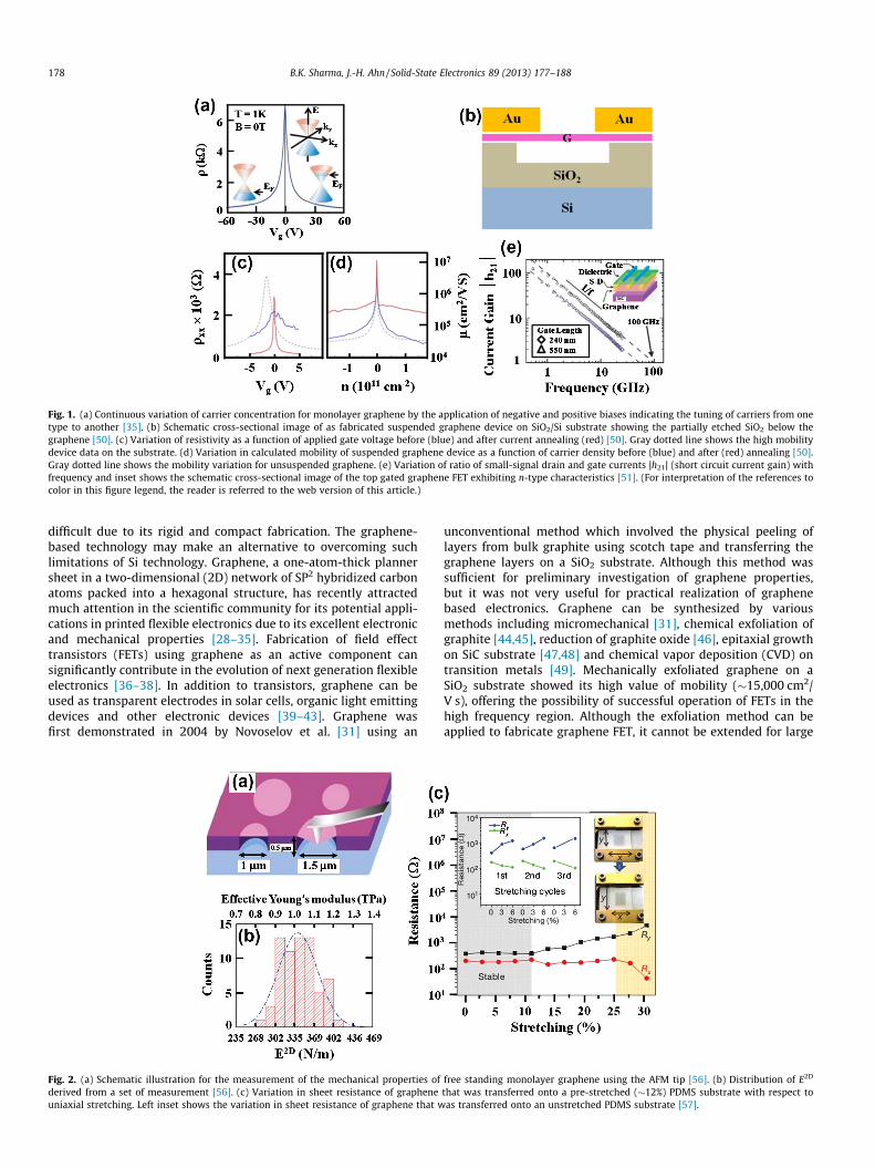
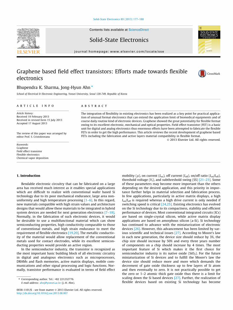
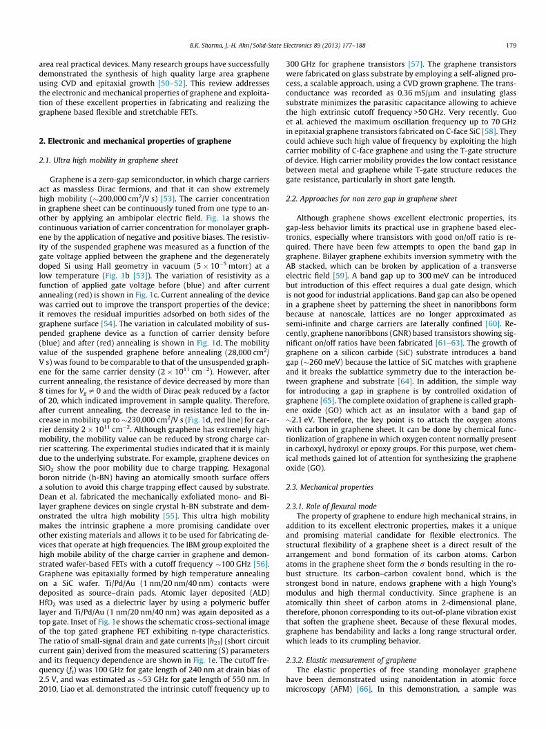
Fig. 1. (a) Continuous variation of carrier concentration for monolayer graphene by the application of negative and positive biases indicating the tuning of carriers from onetype to another [35]. (b) Schematic cross-sectional image of as fabricated suspended graphene device on SiO2/Si substrate showing the partially etched SiO2 below thegraphene [50]. (c) Variation of resistivity as a function of applied gate voltage before (blue) and after current annealing (red) [50]. Gray dotted line shows the high mobilitydevice data on the substrate. (d) Variation in calculated mobility of suspended graphene device as a function of carrier density before (blue) and after (red) annealing [50].Gray dotted line shows the mobility variation for unsuspended graphene. (e) Variation of ratio of small-signal drain and gate currents |h21| (short circuit current gain) withfrequency and inset shows the schematic cross-sectional image of the top gated graphene FET exhibiting n-type characteristics [51]. (For interpretation of the references tocolor in this figure legend, the reader is referred to the web version of this article.)
178 B.K. Sharma, J.-H. Ahn / Solid-State Electronics 89 (2013) 177–188
difficult due to its rigid and compact fabrication. The graphene-based technology may make an alternative to overcoming suchlimitations of Si technology. Graphene, a one-atom-thick plannersheet in a two-dimensional (2D) network of SP2 hybridized carbonatoms packed into a hexagonal structure, has recently attractedmuch attention in the scientific community for its potential appli-cations in printed flexible electronics due to its excellent electronicand mechanical properties [28–35]. Fabrication of field effecttransistors (FETs) using graphene as an active component cansignificantly contribute in the evolution of next generation flexibleelectronics [36–38]. In addition to transistors, graphene can beused as transparent electrodes in solar cells, organic light emittingdevices and other electronic devices [39–43]. Graphene wasfirst demonstrated in 2004 by Novoselov et al. [31] using an
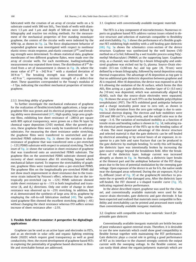
Fig. 2. (a) Schematic illustration for the measurement of the mechanical properties ofderived from a set of measurement [56]. (c) Variation in sheet resistance of grapheneuniaxial stretching. Left inset shows the variation in sheet resistance of graphene that w
unconventional method which involved the physical peeling oflayers from bulk graphite using scotch tape and transferring thegraphene layers on a SiO2 substrate. Although this method wassufficient for preliminary investigation of graphene properties,but it was not very useful for practical realization of graphenebased electronics. Graphene can be synthesized by variousmethods including micromechanical [31], chemical exfoliation ofgraphite [44,45], reduction of graphite oxide [46], epitaxial growthon SiC substrate [47,48] and chemical vapor deposition (CVD) ontransition metals [49]. Mechanically exfoliated graphene on aSiO2 substrate showed its high value of mobility (�15,000 cm2/V s), offering the possibility of successful operation of FETs in thehigh frequency region. Although the exfoliation method can beapplied to fabricate graphene FET, it cannot be extended for large
free standing monolayer graphene using the AFM tip [56]. (b) Distribution of E2D
that was transferred onto a pre-stretched (�12%) PDMS substrate with respect toas transferred onto an unstretched PDMS substrate [57].
B.K. Sharma, J.-H. Ahn / Solid-State Electronics 89 (2013) 177–188 179
area real practical devices. Many research groups have successfullydemonstrated the synthesis of high quality large area grapheneusing CVD and epitaxial growth [50–52]. This review addressesthe electronic and mechanical properties of graphene and exploita-tion of these excellent properties in fabricating and realizing thegraphene based flexible and stretchable FETs.
2. Electronic and mechanical properties of graphene
2.1. Ultra high mobility in graphene sheet
Graphene is a zero-gap semiconductor, in which charge carriersact as massless Dirac fermions, and that it can show extremelyhigh mobility (�200,000 cm2/V s) [53]. The carrier concentrationin graphene sheet can be continuously tuned from one type to an-other by applying an ambipolar electric field. Fig. 1a shows thecontinuous variation of carrier concentration for monolayer graph-ene by the application of negative and positive biases. The resistiv-ity of the suspended graphene was measured as a function of thegate voltage applied between the graphene and the degeneratelydoped Si using Hall geometry in vacuum (5 � 10�5 mtorr) at alow temperature (Fig. 1b [53]). The variation of resistivity as afunction of applied gate voltage before (blue) and after currentannealing (red) is shown in Fig. 1c. Current annealing of the devicewas carried out to improve the transport properties of the device;it removes the residual impurities adsorbed on both sides of thegraphene surface [54]. The variation in calculated mobility of sus-pended graphene device as a function of carrier density before(blue) and after (red) annealing is shown in Fig. 1d. The mobilityvalue of the suspended graphene before annealing (28,000 cm2/V s) was found to be comparable to that of the unsuspended graph-ene for the same carrier density (2 � 1011 cm�2). However, aftercurrent annealing, the resistance of device decreased by more than8 times for Vg – 0 and the width of Dirac peak reduced by a factorof 20, which indicated improvement in sample quality. Therefore,after current annealing, the decrease in resistance led to the in-crease in mobility up to �230,000 cm2/V s (Fig. 1d, red line) for car-rier density 2 � 1011 cm�2. Although graphene has extremely highmobility, the mobility value can be reduced by strong charge car-rier scattering. The experimental studies indicated that it is mainlydue to the underlying substrate. For example, graphene devices onSiO2 show the poor mobility due to charge trapping. Hexagonalboron nitride (h-BN) having an atomically smooth surface offersa solution to avoid this charge trapping effect caused by substrate.Dean et al. fabricated the mechanically exfoliated mono- and Bi-layer graphene devices on single crystal h-BN substrate and dem-onstrated the ultra high mobility [55]. This ultra high mobilitymakes the intrinsic graphene a more promising candidate overother existing materials and allows it to be used for fabricating de-vices that operate at high frequencies. The IBM group exploited thehigh mobile ability of the charge carrier in graphene and demon-strated wafer-based FETs with a cutoff frequency �100 GHz [56].Graphene was epitaxially formed by high temperature annealingon a SiC wafer. Ti/Pd/Au (1 nm/20 nm/40 nm) contacts weredeposited as source–drain pads. Atomic layer deposited (ALD)HfO2 was used as a dielectric layer by using a polymeric bufferlayer and Ti/Pd/Au (1 nm/20 nm/40 nm) was again deposited as atop gate. Inset of Fig. 1e shows the schematic cross-sectional imageof the top gated graphene FET exhibiting n-type characteristics.The ratio of small-signal drain and gate currents |h21| (short circuitcurrent gain) derived from the measured scattering (S) parametersand its frequency dependence are shown in Fig. 1e. The cutoff fre-quency (ft) was 100 GHz for gate length of 240 nm at drain bias of2.5 V, and was estimated as �53 GHz for gate length of 550 nm. In2010, Liao et al. demonstrated the intrinsic cutoff frequency up to
300 GHz for graphene transistors [57]. The graphene transistorswere fabricated on glass substrate by employing a self-aligned pro-cess, a scalable approach, using a CVD grown graphene. The trans-conductance was recorded as 0.36 mS/lm and insulating glasssubstrate minimizes the parasitic capacitance allowing to achievethe high extrinsic cutoff frequency >50 GHz. Very recently, Guoet al. achieved the maximum oscillation frequency up to 70 GHzin epitaxial graphene transistors fabricated on C-face SiC [58]. Theycould achieve such high value of frequency by exploiting the highcarrier mobility of C-face graphene and using the T-gate structureof device. High carrier mobility provides the low contact resistancebetween metal and graphene while T-gate structure reduces thegate resistance, particularly in short gate length.
2.2. Approaches for non zero gap in graphene sheet
Although graphene shows excellent electronic properties, itsgap-less behavior limits its practical use in graphene based elec-tronics, especially where transistors with good on/off ratio is re-quired. There have been few attempts to open the band gap ingraphene. Bilayer graphene exhibits inversion symmetry with theAB stacked, which can be broken by application of a transverseelectric field [59]. A band gap up to 300 meV can be introducedbut introduction of this effect requires a dual gate design, whichis not good for industrial applications. Band gap can also be openedin a graphene sheet by patterning the sheet in nanoribbons formbecause at nanoscale, lattices are no longer approximated assemi-infinite and charge carriers are laterally confined [60]. Re-cently, graphene nanoribbons (GNR) based transistors showing sig-nificant on/off ratios have been fabricated [61–63]. The growth ofgraphene on a silicon carbide (SiC) substrate introduces a bandgap (�260 meV) because the lattice of SiC matches with grapheneand it breaks the sublattice symmetry due to the interaction be-tween graphene and substrate [64]. In addition, the simple wayfor introducing a gap in graphene is by controlled oxidation ofgraphene [65]. The complete oxidation of graphene is called graph-ene oxide (GO) which act as an insulator with a band gap of�2.1 eV. Therefore, the key point is to attach the oxygen atomswith carbon in graphene sheet. It can be done by chemical func-tionlization of graphene in which oxygen content normally presentin carboxyl, hydroxyl or epoxy groups. For this purpose, wet chem-ical methods gained lot of attention for synthesizing the grapheneoxide (GO).
2.3. Mechanical properties
2.3.1. Role of flexural modeThe property of graphene to endure high mechanical strains, in
addition to its excellent electronic properties, makes it a uniqueand promising material candidate for flexible electronics. Thestructural flexibility of a graphene sheet is a direct result of thearrangement and bond formation of its carbon atoms. Carbonatoms in the graphene sheet form the r bonds resulting in the ro-bust structure. Its carbon–carbon covalent bond, which is thestrongest bond in nature, endows graphene with a high Young’smodulus and high thermal conductivity. Since graphene is anatomically thin sheet of carbon atoms in 2-dimensional plane,therefore, phonon corresponding to its out-of-plane vibration existthat soften the graphene sheet. Because of these flexural modes,graphene has bendability and lacks a long range structural order,which leads to its crumpling behavior.
2.3.2. Elastic measurement of grapheneThe elastic properties of free standing monolayer graphene
have been demonstrated using nanoidentation in atomic forcemicroscopy (AFM) [66]. In this demonstration, a sample was
180 B.K. Sharma, J.-H. Ahn / Solid-State Electronics 89 (2013) 177–188
fabricated with the creation of an array of circular wells on a Sisubstrate coated with 300 nm SiO2. Two kinds of wells with diam-eters 1.5 lm and 1 lm and depth of 500 nm were defined bylithography and reactive ion etching methods. For the measure-ment of the mechanical properties of free standing monolayergraphene, the centers of the circular wells were indented by theAFM tip, as shown in Fig. 2a. The force–displacement behavior ofsuspended graphene was investigated with respect to nonlinearelastic stress–strain response, and elastic constant (E2D) and break-ing strength were determined. To obtain statistical data, graphenemembranes of two different graphene flakes, were made over thearray of circular wells. For each membrane, loading/unloadingmeasurement was repeated three times. The distribution of E2D de-rived from a set of measurement is shown in Fig. 2b, where themean value of E2D is �342 N m�1 with a standard deviation of30 N m�1. The breaking strength was determined to be�42 N m�1, representing the intrinsic strength of a defect-freesheet. These quantities corresponded to the Young’s modulus of�1 Tpa, indicating the excellent mechanical properties of intrinsicgraphene.
2.3.3. Stretching ability of grapheneTo further investigate the mechanical endurance of graphene
for the realization of flexible/stretchable applications, a large areagraphene film was grown and its electrical properties and stretch-ing ability were demonstrated [67]. High quality, large area graph-ene films, exhibiting low sheet resistance of �280 X per squarewith 80% optical transparency, were grown on a thin Ni layer bychemical vapor deposition (CVD) method. After the growth pro-cess, these graphene films were easily be transferred to arbitrarysubstrates. For measuring the sheet resistance under stretching,the graphene films were transferred to unstretched and pre-stretched PDMS substrates. Fig. 2c shows the variation in sheetresistance of graphene that was transferred onto a pre-stretched(�12%) PDMS substrate with respect to uniaxial stretching. The leftinset of Fig. 2c shows the variation in sheet resistance of graphenethat was transferred onto an unstretched PDMS substrate. Thegraphene film on the unstretched PDMS substrate showed goodrecovery of sheet resistance after 6% stretching, beyond whichmechanical failure started. To improve the stretchability of graph-ene, graphene films were transferred onto a pre-stretched PDMS.The graphene film on the longitudinally pre-stretched PDMS didnot show much improvement in sheet resistance due to the trans-verse strain induced by Poisson’s effect, whereas that on the iso-tropically pre-stretched (up to �12%) PDMS substrate showedstable sheet resistance up to �11% in both longitudinal and trans-verse (Rx and Ry) directions. Only one order of change in sheetresistance was observed up to �25% stretching. In addition, Baeet al. demonstrated the synthesis of large area 30 in. graphene byemploying the roll-to-roll fabrication method [49]. The synthe-sized graphene film showed the excellent stretching ability (�6%)without changing the sheet resistance whereas ITO suffers seriousincrease of sheet resistance after �2.5%.
3. Flexible field effect transistor: A perspective for digital/logicapplications
Graphene can be used as an active layer and electrodes in FETs,and as an electrode in solar cells and organic lighting emittingdiode (OLED) which require good transparency as well as goodconductivity. Here, the recent development of graphene based FETsin exploring the potentiality of graphene based electronic in flexi-ble and stretchable format are addressed.
3.1. Graphene with conventionally available inorganic materials
The FETs is a key component of microelectronics. Numerous re-ports on graphene based FETs address various issues related to de-vice structure and selection of materials compatible to flexibilityand stretchability. Fig. 3 shows the performance of a flexible graph-ene FET exhibiting high mobility with a self healing gate dielectric[68]. Fig. 3a shows the schematics cross-section of the devicestructure. Graphene was synthesized by the well known CVDmethod on a Cu foil, followed by a wet transfer process using Poly(-methyl Methacrylate) (PMMA) as the supporting layer. Graphenestrip, as a channel, was defined by e-beam lithography and unde-sired graphene was etched out by O2 plasma. Source–Drain elec-trodes (0.5 nm Cr/60 nm Au) and top gate (Al, 70 nm) weredefined by e-beam lithography, followed by metal deposition usingthermal evaporation. The advantage of Al deposition as top gate isthat no additional gate dielectric deposition between graphene andAl is required. After Al deposition, the device was exposed to air for6 h allowing the oxidation of the Al surface, which forms the thinAlOx film acting as a gate dielectric. Another layer of Cr (0.5 nm)/Au (10 nm) was deposited, which was automatically aligned byAl/AlOx such that the source–drain electrodes were separated.Fig. 3b shows the array of such TFTs on the bendable poly(ethyleneterephthalate) (PET). The FETs exhibited good ambipolar behaviorand a charge neutrality point near to zero volt, as shown inFig. 3c. Little deviation from the zero gate voltage is due to unin-tentional electron doping. The electron and hole mobilities were230 and 300 cm2/V s, respectively, and the on/off ratio was in therange �3–6. The variation of normalized mobility as a function oftensile strain and bending radius is shown in Fig. 3d, indicating sta-ble electrical performance of the FETs up to the bending radius of�8 mm. The most important advantage of this device structureand selected material is that the gate dielectric can be self-healedby electrical annealing or by several hours of air exposure, in re-sponse to a pin hole and nano fracture that can be produced inthe gate dielectric by multiple bending. To verify this self-healing,the dielectric layer was intentionally broken by increasing thegate-source voltage beyond the breakdown field. After the break-down of the dielectric layer, leakage current was increasedabruptly as shown in Fig. 3e. Normally, a dielectric layer breaksat the thinnest part and the ambiploar behavior of the FET disap-pears due to the loss of potential modulation by the sweeping gatevoltage. Upon exposure of the device to air for 6 h, the native oxidenear the damaged areas reformed. During the air exposure, H2O orO2 diffused (inset of Fig. 3f) at the graphene/Al interface to pro-mote the re-growth of the damaged area. After the dielectric layerself-healed, the FET showed a v-shaped transfer curve (Fig. 3f),indicating regained device performance.
In the above described report, graphene was used for the chan-nel, and conventionally available materials were used for thesource–drain electrodes, gate dielectric and gate electrode. It hasbeen expected and realized that materials more compatible to flex-ibility and stretchability can be printed and processed more easilythan conventionally available inorganic materials.
3.2. Graphene with compatible active layer materials: Search forprintable gate dielectric
Conventionally available inorganic materials are brittle becauseof poor endurance against external strain. Therefore, it is desirableto use the new materials which could show good compatibility inflexible format together with maintaining the FET performance.Gate dielectric plays a crucial role in getting a good performanceof FET as its interface to the channel strongly controls the outputcurrent with the sweeping voltage. In the flexible context, wecan easily think about the organic/polymeric materials which are
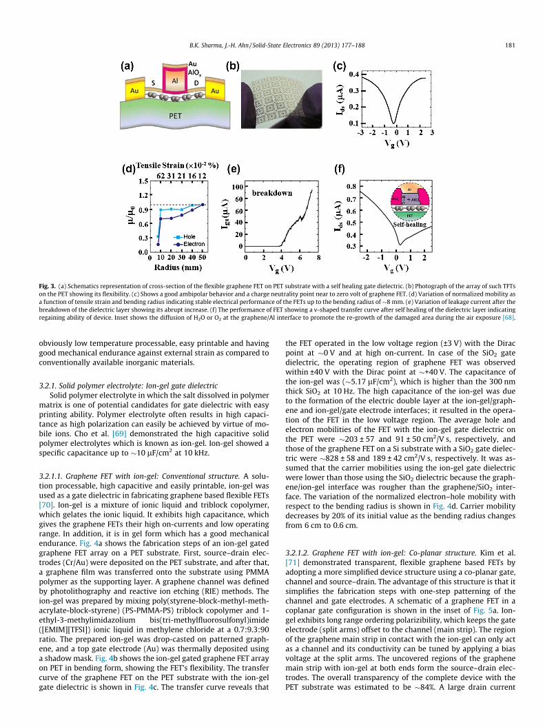
Fig. 3. (a) Schematics representation of cross-section of the flexible graphene FET on PET substrate with a self healing gate dielectric. (b) Photograph of the array of such TFTson the PET showing its flexibility. (c) Shows a good ambipolar behavior and a charge neutrality point near to zero volt of graphene FET. (d) Variation of normalized mobility asa function of tensile strain and bending radius indicating stable electrical performance of the FETs up to the bending radius of�8 mm. (e) Variation of leakage current after thebreakdown of the dielectric layer showing its abrupt increase. (f) The performance of FET showing a v-shaped transfer curve after self healing of the dielectric layer indicatingregaining ability of device. Inset shows the diffusion of H2O or O2 at the graphene/Al interface to promote the re-growth of the damaged area during the air exposure [68].
B.K. Sharma, J.-H. Ahn / Solid-State Electronics 89 (2013) 177–188 181
obviously low temperature processable, easy printable and havinggood mechanical endurance against external strain as compared toconventionally available inorganic materials.
3.2.1. Solid polymer electrolyte: Ion-gel gate dielectricSolid polymer electrolyte in which the salt dissolved in polymer
matrix is one of potential candidates for gate dielectric with easyprinting ability. Polymer electrolyte often results in high capaci-tance as high polarization can easily be achieved by virtue of mo-bile ions. Cho et al. [69] demonstrated the high capacitive solidpolymer electrolytes which is known as ion-gel. Ion-gel showed aspecific capacitance up to �10 lF/cm2 at 10 kHz.
3.2.1.1. Graphene FET with ion-gel: Conventional structure. A solu-tion processable, high capacitive and easily printable, ion-gel wasused as a gate dielectric in fabricating graphene based flexible FETs[70]. Ion-gel is a mixture of ionic liquid and triblock copolymer,which gelates the ionic liquid. It exhibits high capacitance, whichgives the graphene FETs their high on-currents and low operatingrange. In addition, it is in gel form which has a good mechanicalendurance. Fig. 4a shows the fabrication steps of an ion-gel gatedgraphene FET array on a PET substrate. First, source–drain elec-trodes (Cr/Au) were deposited on the PET substrate, and after that,a graphene film was transferred onto the substrate using PMMApolymer as the supporting layer. A graphene channel was definedby photolithography and reactive ion etching (RIE) methods. Theion-gel was prepared by mixing poly(styrene-block-methyl-meth-acrylate-block-styrene) (PS-PMMA-PS) triblock copolymer and 1-ethyl-3-methylimidazolium bis(tri-methylfluorosulfonyl)imide([EMIM][TFSI]) ionic liquid in methylene chloride at a 0.7:9.3:90ratio. The prepared ion-gel was drop-casted on patterned graph-ene, and a top gate electrode (Au) was thermally deposited usinga shadow mask. Fig. 4b shows the ion-gel gated graphene FET arrayon PET in bending form, showing the FET’s flexibility. The transfercurve of the graphene FET on the PET substrate with the ion-gelgate dielectric is shown in Fig. 4c. The transfer curve reveals that
the FET operated in the low voltage region (±3 V) with the Diracpoint at �0 V and at high on-current. In case of the SiO2 gatedielectric, the operating region of graphene FET was observedwithin ±40 V with the Dirac point at �+40 V. The capacitance ofthe ion-gel was (�5.17 lF/cm2), which is higher than the 300 nmthick SiO2 at 10 Hz. The high capacitance of the ion-gel was dueto the formation of the electric double layer at the ion-gel/graph-ene and ion-gel/gate electrode interfaces; it resulted in the opera-tion of the FET in the low voltage region. The average hole andelectron mobilities of the FET with the ion-gel gate dielectric onthe PET were �203 ± 57 and 91 ± 50 cm2/V s, respectively, andthose of the graphene FET on a Si substrate with a SiO2 gate dielec-tric were �828 ± 58 and 189 ± 42 cm2/V s, respectively. It was as-sumed that the carrier mobilities using the ion-gel gate dielectricwere lower than those using the SiO2 dielectric because the graph-ene/ion-gel interface was rougher than the graphene/SiO2 inter-face. The variation of the normalized electron–hole mobility withrespect to the bending radius is shown in Fig. 4d. Carrier mobilitydecreases by 20% of its initial value as the bending radius changesfrom 6 cm to 0.6 cm.
3.2.1.2. Graphene FET with ion-gel: Co-planar structure. Kim et al.[71] demonstrated transparent, flexible graphene based FETs byadopting a more simplified device structure using a co-planar gate,channel and source–drain. The advantage of this structure is that itsimplifies the fabrication steps with one-step patterning of thechannel and gate electrodes. A schematic of a graphene FET in acoplanar gate configuration is shown in the inset of Fig. 5a. Ion-gel exhibits long range ordering polarizibility, which keeps the gateelectrode (split arms) offset to the channel (main strip). The regionof the graphene main strip in contact with the ion-gel can only actas a channel and its conductivity can be tuned by applying a biasvoltage at the split arms. The uncovered regions of the graphenemain strip with ion-gel at both ends form the source–drain elec-trodes. The overall transparency of the complete device with thePET substrate was estimated to be �84%. A large drain current
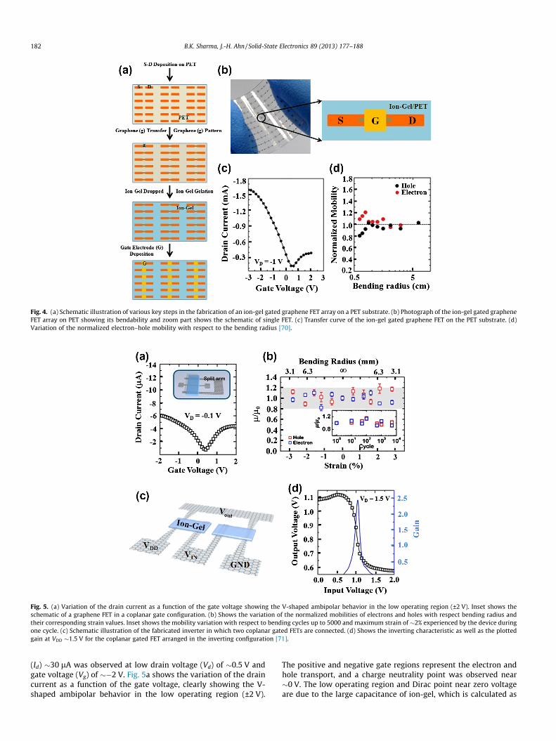
Fig. 4. (a) Schematic illustration of various key steps in the fabrication of an ion-gel gated graphene FET array on a PET substrate. (b) Photograph of the ion-gel gated grapheneFET array on PET showing its bendability and zoom part shows the schematic of single FET. (c) Transfer curve of the ion-gel gated graphene FET on the PET substrate. (d)Variation of the normalized electron–hole mobility with respect to the bending radius [70].
Fig. 5. (a) Variation of the drain current as a function of the gate voltage showing the V-shaped ambipolar behavior in the low operating region (±2 V). Inset shows theschematic of a graphene FET in a coplanar gate configuration. (b) Shows the variation of the normalized mobilities of electrons and holes with respect bending radius andtheir corresponding strain values. Inset shows the mobility variation with respect to bending cycles up to 5000 and maximum strain of �2% experienced by the device duringone cycle. (c) Schematic illustration of the fabricated inverter in which two coplanar gated FETs are connected. (d) Shows the inverting characteristic as well as the plottedgain at VDD �1.5 V for the coplanar gated FET arranged in the inverting configuration [71].
182 B.K. Sharma, J.-H. Ahn / Solid-State Electronics 89 (2013) 177–188
(Id) �30 lA was observed at low drain voltage (Vd) of �0.5 V andgate voltage (Vg) of ��2 V. Fig. 5a shows the variation of the draincurrent as a function of the gate voltage, clearly showing the V-shaped ambipolar behavior in the low operating region (±2 V).
The positive and negative gate regions represent the electron andhole transport, and a charge neutrality point was observed near�0 V. The low operating region and Dirac point near zero voltageare due to the large capacitance of ion-gel, which is calculated as
B.K. Sharma, J.-H. Ahn / Solid-State Electronics 89 (2013) 177–188 183
�8.1 lF/cm2 in metal/insulator/metal coplanar electrode structure.The calculation of mobility in the coplanar structure is slightly dif-ferent from that of mobility in the conventional structure. In thecoplanar structure, the resistivity of the source–drain electrodes(contributed by the main strip region which is not covered byion-gel) becomes higher than that of the channel (the region cov-ered by ion-gel) when the FET is on. To calculate the channel resis-tance accurately, electrodes resistance were subtracted from thetotal resistance and mobility was calculated. The average holeand electron mobilities of the coplanar gated graphene based FETwere estimated to be �892 ± 196 and 628 ± 146 cm2/V s respec-tively. The mechanical flexibility and robustness of devices wereinvestigated by bending tests in forward and backward directions.Fig. 5b shows the variation of the normalized mobilities of elec-trons and holes with respect to bending radius and their corre-sponding strain values; the maximum change in mobility is�20% within the strain of 2.8%. The inset of Fig. 5b shows themobility variation with respect to bending cycles up to 5000 andmaximum strain of �2%. The maximum change in mobility duringrepeated cyclic tests was found to be within 20%. This indicatesthat the device showed the good reliability and stable performanceduring mechanical deformation. By taking advantage of the simpli-fied coplanar FET structure, a complementary graphene based in-verter was fabricated on a PET substrate. Fig. 5c shows theschematics of the fabricated inverter, in which two coplanar gatedFETs are connected. Both the transistor share a common input (VIN)and output (VOUT) and the supply voltage (VDD) is applied to onetransistor while other is grounded (GND). For a single grapheneFET, the Dirac point shifted as a function of drain voltage. In the in-verter configuration, the two identical FETs showed different Diracpoints depending on the distribution of the supply voltage acrossthem during the sweeping of the input voltage (VIN), which as a re-sult, lead to the inverter characteristics. Fig. 5d shows the invertingcharacteristic as well as the plotted gain at VDD �1.5 V for thecoplanar gated FET arranged in the inverting configuration. Themaximum gain of the inverter in this coplanar configuration is cal-culated to be �2.6.
3.2.1.3. Integration of stretchability. In addition to the flexibility,stretchability is also needed in graphene based FETs for practicalrealization of conformal and wearable devices. Lee et al. carriedout significant investigations with respect to stretchability, dem-onstrating a graphene based FET with ion-gel gate dielectric on astretchable substrate by transfer and aerosol printing methodswith low temperature processing [72]. The graphene patterned di-rectly on Cu foil was transferred onto a rubber-like substrate. Anion-gel gate dielectric was printed by the aerosol jet printing meth-od having printing resolution of �50 lm. A poly(3,4-ethylenedi-oxythiophene) oxidized with poly(4-styrenesulfonate)(PEDOT:PSS) was printed as a gate electrode by covering the chan-nel region. The use of ion-gel as a gate dielectric enables the quickformation of an electric double layer, regardless of the area of over-lap between the gate electrode and the active channel region as itrelies on the motion of the mobile ions. Initially, the FET was fab-ricated using monolayer graphene in the channel region, whichshowed the V-shaped ambipolar behavior at VD = �0.1 V. The aver-age hole and electron mobilities were estimated to be �26 and20 cm2/V s, respectively. The low value of mobility in the mono-layer graphene based FET was due to scattering from the molecularspecies inside the porous structure of the PDMS and to exposure ofgraphene devices to contaminating species, which reduced thetransport of carriers in graphene. To overcome these effects, bi-and tri-layer graphene channels were used to fabricate the FET.The advantage of using bi- or tri-layer graphene as a channel is thatthe bottom layer provides sufficient screening of charges species inthe porous structure of the PDMS and that the top layer suppresses
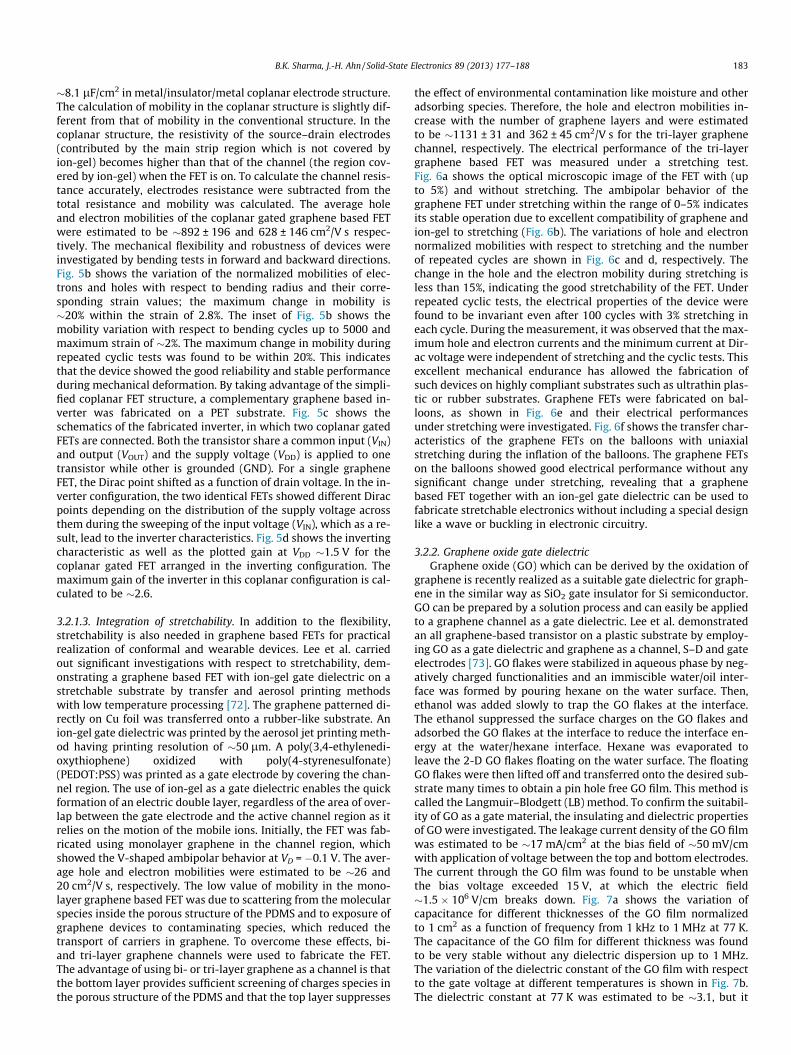
the effect of environmental contamination like moisture and otheradsorbing species. Therefore, the hole and electron mobilities in-crease with the number of graphene layers and were estimatedto be �1131 ± 31 and 362 ± 45 cm2/V s for the tri-layer graphenechannel, respectively. The electrical performance of the tri-layergraphene based FET was measured under a stretching test.Fig. 6a shows the optical microscopic image of the FET with (upto 5%) and without stretching. The ambipolar behavior of thegraphene FET under stretching within the range of 0–5% indicatesits stable operation due to excellent compatibility of graphene andion-gel to stretching (Fig. 6b). The variations of hole and electronnormalized mobilities with respect to stretching and the numberof repeated cycles are shown in Fig. 6c and d, respectively. Thechange in the hole and the electron mobility during stretching isless than 15%, indicating the good stretchability of the FET. Underrepeated cyclic tests, the electrical properties of the device werefound to be invariant even after 100 cycles with 3% stretching ineach cycle. During the measurement, it was observed that the max-imum hole and electron currents and the minimum current at Dir-ac voltage were independent of stretching and the cyclic tests. Thisexcellent mechanical endurance has allowed the fabrication ofsuch devices on highly compliant substrates such as ultrathin plas-tic or rubber substrates. Graphene FETs were fabricated on bal-loons, as shown in Fig. 6e and their electrical performancesunder stretching were investigated. Fig. 6f shows the transfer char-acteristics of the graphene FETs on the balloons with uniaxialstretching during the inflation of the balloons. The graphene FETson the balloons showed good electrical performance without anysignificant change under stretching, revealing that a graphenebased FET together with an ion-gel gate dielectric can be used tofabricate stretchable electronics without including a special designlike a wave or buckling in electronic circuitry.
3.2.2. Graphene oxide gate dielectricGraphene oxide (GO) which can be derived by the oxidation of
graphene is recently realized as a suitable gate dielectric for graph-ene in the similar way as SiO2 gate insulator for Si semiconductor.GO can be prepared by a solution process and can easily be appliedto a graphene channel as a gate dielectric. Lee et al. demonstratedan all graphene-based transistor on a plastic substrate by employ-ing GO as a gate dielectric and graphene as a channel, S–D and gateelectrodes [73]. GO flakes were stabilized in aqueous phase by neg-atively charged functionalities and an immiscible water/oil inter-face was formed by pouring hexane on the water surface. Then,ethanol was added slowly to trap the GO flakes at the interface.The ethanol suppressed the surface charges on the GO flakes andadsorbed the GO flakes at the interface to reduce the interface en-ergy at the water/hexane interface. Hexane was evaporated toleave the 2-D GO flakes floating on the water surface. The floatingGO flakes were then lifted off and transferred onto the desired sub-strate many times to obtain a pin hole free GO film. This method iscalled the Langmuir–Blodgett (LB) method. To confirm the suitabil-ity of GO as a gate material, the insulating and dielectric propertiesof GO were investigated. The leakage current density of the GO filmwas estimated to be �17 mA/cm2 at the bias field of �50 mV/cmwith application of voltage between the top and bottom electrodes.The current through the GO film was found to be unstable whenthe bias voltage exceeded 15 V, at which the electric field�1.5 � 106 V/cm breaks down. Fig. 7a shows the variation ofcapacitance for different thicknesses of the GO film normalizedto 1 cm2 as a function of frequency from 1 kHz to 1 MHz at 77 K.The capacitance of the GO film for different thickness was foundto be very stable without any dielectric dispersion up to 1 MHz.The variation of the dielectric constant of the GO film with respectto the gate voltage at different temperatures is shown in Fig. 7b.The dielectric constant at 77 K was estimated to be �3.1, but it
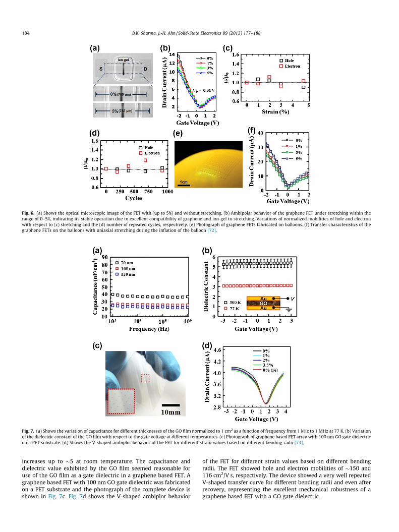
Fig. 6. (a) Shows the optical microscopic image of the FET with (up to 5%) and without stretching. (b) Ambipolar behavior of the graphene FET under stretching within therange of 0–5%, indicating its stable operation due to excellent compatibility of graphene and ion-gel to stretching. Variations of normalized mobilities of hole and electronwith respect to (c) stretching and the (d) number of repeated cycles, respectively. (e) Photograph of graphene FETs fabricated on balloons. (f) Transfer characteristics of thegraphene FETs on the balloons with uniaxial stretching during the inflation of the balloon [72].
Fig. 7. (a) Shows the variation of capacitance for different thicknesses of the GO film normalized to 1 cm2 as a function of frequency from 1 kHz to 1 MHz at 77 K. (b) Variationof the dielectric constant of the GO film with respect to the gate voltage at different temperatures. (c) Photograph of graphene based FET array with 100 nm GO gate dielectricon a PET substrate. (d) Shows the V-shaped ambiplor behavior of the FET for different strain values based on different bending radii [73].
184 B.K. Sharma, J.-H. Ahn / Solid-State Electronics 89 (2013) 177–188
increases up to �5 at room temperature. The capacitance anddielectric value exhibited by the GO film seemed reasonable foruse of the GO film as a gate dielectric in a graphene based FET. Agraphene based FET with 100 nm GO gate dielectric was fabricatedon a PET substrate and the photograph of the complete device isshown in Fig. 7c. Fig. 7d shows the V-shaped ambiplor behavior
of the FET for different strain values based on different bendingradii. The FET showed hole and electron mobilities of �150 and116 cm2/V s, respectively. The device showed a very well repeatedV-shaped transfer curve for different bending radii and even afterrecovery, representing the excellent mechanical robustness of agraphene based FET with a GO gate dielectric.
B.K. Sharma, J.-H. Ahn / Solid-State Electronics 89 (2013) 177–188 185
The above reviewed recent work mainly focused on the devel-opment of graphene based FETs in flexible format showing pooron/off ratio which does not fulfill the requirement for the potentialuse of these FETs in digital applications. For realizing the graphenebased digital/logic applications it is quite important to open theband gap in graphene (see Section 2.2).
4. High frequency flexible field effect transistor: A perspectivefor analogue/radio frequency applications
Zero band gap of graphene is the main hurdle in fabricating thegraphene based digital applications. On the other hand, its ultrahigh mobility, current carrying capacity and saturation velocity of-fer the fabrication of radio frequencies (r.f.) electronic deviceswhere a large on/off ratio in FET is not necessary. In this context,several groups have been demonstrated the high frequency graph-ene based FET [56,74,75]. The fabrication of graphene based r.f. de-vices is also demanding for realizing the real applications of plasticelectronics. Recently, few attempts have been taken in this direc-tion using CVD grown graphene as well as solution basedgraphene.
4.1. Solution based single layer graphene for flexible gigahertztransistor
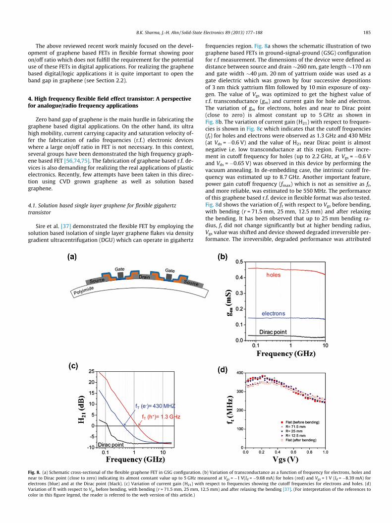
Sire et al. [37] demonstrated the flexible FET by employing thesolution based isolation of single layer graphene flakes via densitygradient ultracentrifugation (DGU) which can operate in gigahertz
Fig. 8. (a) Schematic cross-sectional of the flexible graphene FET in GSG configuration. (near to Dirac point (close to zero) indicating its almost constant value up to 5 GHz meaelectrons (blue) and at the Dirac point (black). (c) Variation of current gain (H21) withVariation of ft with respect to Vgs before bending, with bending (r = 71.5 mm, 25 mm, 12color in this figure legend, the reader is referred to the web version of this article.)
frequencies region. Fig. 8a shows the schematic illustration of twographene based FETs in ground-signal-ground (GSG) configurationfor r.f measurement. The dimensions of the device were defined asdistance between source and drain �260 nm, gate length �170 nmand gate width �40 lm. 20 nm of yattrium oxide was used as agate dielectric which was grown by four successive depositionsof 3 nm thick yattrium film followed by 10 min exposure of oxy-gen. The value of Vgs was optimized to get the highest value ofr.f. transconductance (gm) and current gain for hole and electron.The variation of gm for electrons, holes and near to Dirac point(close to zero) is almost constant up to 5 GHz as shown inFig. 8b. The variation of current gain (H21) with respect to frequen-cies is shown in Fig. 8c which indicates that the cutoff frequencies(ft) for holes and electrons were observed as 1.3 GHz and 430 MHz(at Vds = �0.6 V) and the value of H21 near Dirac point is almostnegative i.e. low transconductance at this region. Further incre-ment in cutoff frequency for holes (up to 2.2 GHz, at Vgs = �0.6 Vand Vds = �0.65 V) was observed in this device by performing thevacuum annealing. In de-embedding case, the intrinsic cutoff fre-quency was estimated up to 8.7 GHz. Another important feature,power gain cutoff frequency (fmax) which is not as sensitive as ft,and more reliable, was estimated to be 550 MHz. The performanceof this graphene based r.f. device in flexible format was also tested.Fig. 8d shows the variation of ft with respect to Vgs before bending,with bending (r = 71.5 mm, 25 mm, 12.5 mm) and after relaxingthe bending. It has been observed that up to 25 mm bending ra-dius, ft did not change significantly but at higher bending radius,Vgs value was shifted and device showed degraded irreversible per-formance. The irreversible, degraded performance was attributed
b) Variation of transconductance as a function of frequency for electrons, holes andsured at Vgs = �1 V(Id = �9.68 mA) for holes (red) and Vgs = 1 V (Id = �8.39 mA) forrespect to frequencies showing the cutoff frequencies for electrons and holes. (d).5 mm) and after relaxing the bending [37]. (For interpretation of the references to
186 B.K. Sharma, J.-H. Ahn / Solid-State Electronics 89 (2013) 177–188
to poor contact of graphene flakes that connections become looseupon bending.
4.2. CVD grown graphene based flexible gigahertz transistor
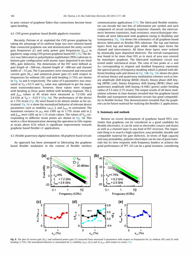
Recently, Petrone et al. exploited the CVD grown graphene bytaking the advantage of its uniform large size over solution basedflaks connected graphene one and demonstrated the unity currentgain frequencies (ft) and unity power gain frequencies (fmax) ingigahertz range using CVD grown graphene based FET [76]. The de-vice was fabricated on polyethylene naphthalate (PEN) substrate inbottom gate configuration with atomic layer deposited 6 nm thickHfO2 gate dielectric. The dimensions of the FET were defined asgate length of �500 nm, channel length of �900 nm and channelwidth of �15 lm. The S-parameters were measured and extractedcurrent gain (H21) and unilateral power gain (U) with respect tofrequencies for without (0%) and with bending (1.75%) are shownin Fig. 9a and b respectively. The value of S-parameters was mea-sured at Vds = 0.5 V and Vgs value was optimized to get the maxi-mum transconductance, however, these values were changedwith bending as Dirac point shifted with bending response. The ft
and fmax values at 0% strain were measured as 7.2 GHz and2.6 GHz at Vgs = �0.25 V (Fig. 9a). The performance of the deviceat 1.75% strain (Fig. 9b) were found to be almost similar as for un-strained. Fig. 9c–e show the normalized behavior of relevant deviceparameters such as mobility (lFE), ft and fmax to unstrained. Themaximum variance in lFE was ±30% up to 1.75% strain and in ft
and fmax were ±20% up to 1.1% strain values. The values of Vgs cor-responding to different strain points are shown in Fig. 9d. Thiswork is a first demonstration showing the operation in GHz regimeat strain above 0.5% which is significant improvement towardsgraphene based flexible r.f. applications.
4.3. Flexible quaternary digital modulation: All graphene based circuits
An approach has been attempted in fabricating the graphenebased flexible modulator in the context of flexible wireless
Fig. 9. The plot of current gain (H21) and unilateral power gain (U) extracted from mebending (1.75%). The normalized behavior to unstrained for (c) mobility (lFE), (d) ft and
communication applications [77]. The fabricated flexible modula-tor can encode the two bits of information per symbol and eachcomponent of circuit including transistor channels, the intercon-nects between transistors, load resistance, source/drain/gate elec-trodes-all were fabricated with graphene owing to flexibility andtransparency. Fig. 10a shows the schematics of all graphene baseddevices fabricated on flexible PEN substrate. The top and bottomlayers form top and bottom gate while middle layer forms thechannel and interconnects. All these three layers were isolatedby atomically layer deposited dielectric. The overall transparencywas found to be more than 93% as in most of area was coveredby monolayer graphene. The fabricated modulator circuit wastested under mechanical strain. The ratio of two peaks at x and2x corresponding to original and doubled frequency representsthe spectral purity of frequency doubling which is plotted with dif-ferent bending radii and shown in Fig. 10b. Fig. 10c shows the plotsof various binary and quaternary modulation schemes such as bin-ary amplitude shift keying (BASK) (black), binary phase shift key-ing (BPSK) (red), binary frequency shift keying (BFSK) (blue) andquaternary amplitude shift keying (4-ASK) (green) under bendingradius of 5.5 mm (2.7% strain). The output results of all these mod-ulation schemes in time domain revealed that the graphene basedflexible and transparent modulation circuits has good compatibil-ity in flexible format. This demonstration revealed that the graph-ene can be future material for realizing the flexible r.f. applications.
5. Summary and outlook
Review on recent development of graphene based FETs con-cludes that graphene can be considered as a good candidate forflexible electronics. It can be used as electrodes (source and drain)as well as a channel layer in any kind of FET structure. The impor-tant thing is to search a high capacitive, easy printable, durable andcompatible material for gate dielectric. In terms of high capacityand easy printability, polymer electrolyte can be one of good mate-rials but its slow response with frequency hinders to achieve thegood performance of TFT. GO can be a good insulator, considering
asured S-parameters with respect to frequencies for (a) without (0%) and (b) with(e) fmax with respect to strain [76].
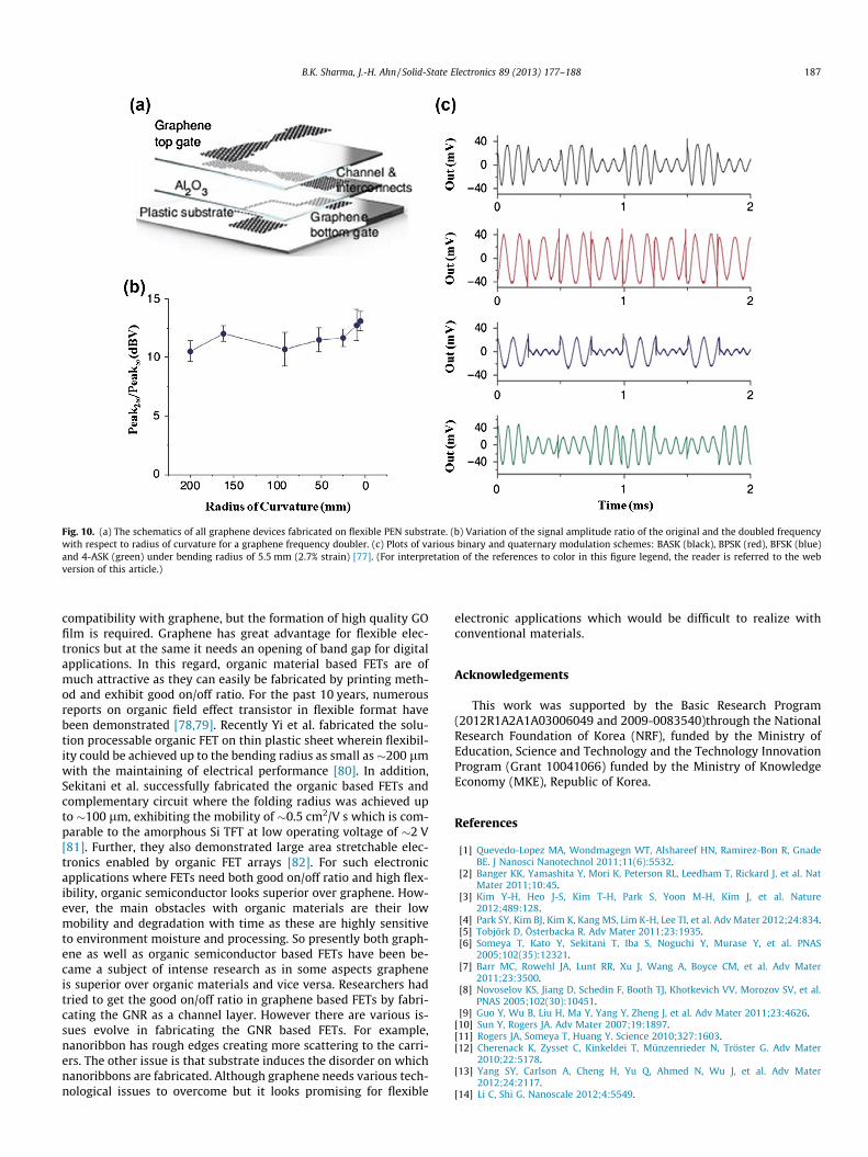
Fig. 10. (a) The schematics of all graphene devices fabricated on flexible PEN substrate. (b) Variation of the signal amplitude ratio of the original and the doubled frequencywith respect to radius of curvature for a graphene frequency doubler. (c) Plots of various binary and quaternary modulation schemes: BASK (black), BPSK (red), BFSK (blue)and 4-ASK (green) under bending radius of 5.5 mm (2.7% strain) [77]. (For interpretation of the references to color in this figure legend, the reader is referred to the webversion of this article.)
B.K. Sharma, J.-H. Ahn / Solid-State Electronics 89 (2013) 177–188 187
compatibility with graphene, but the formation of high quality GOfilm is required. Graphene has great advantage for flexible elec-tronics but at the same it needs an opening of band gap for digitalapplications. In this regard, organic material based FETs are ofmuch attractive as they can easily be fabricated by printing meth-od and exhibit good on/off ratio. For the past 10 years, numerousreports on organic field effect transistor in flexible format havebeen demonstrated [78,79]. Recently Yi et al. fabricated the solu-tion processable organic FET on thin plastic sheet wherein flexibil-ity could be achieved up to the bending radius as small as�200 lmwith the maintaining of electrical performance [80]. In addition,Sekitani et al. successfully fabricated the organic based FETs andcomplementary circuit where the folding radius was achieved upto �100 lm, exhibiting the mobility of �0.5 cm2/V s which is com-parable to the amorphous Si TFT at low operating voltage of �2 V[81]. Further, they also demonstrated large area stretchable elec-tronics enabled by organic FET arrays [82]. For such electronicapplications where FETs need both good on/off ratio and high flex-ibility, organic semiconductor looks superior over graphene. How-ever, the main obstacles with organic materials are their lowmobility and degradation with time as these are highly sensitiveto environment moisture and processing. So presently both graph-ene as well as organic semiconductor based FETs have been be-came a subject of intense research as in some aspects grapheneis superior over organic materials and vice versa. Researchers hadtried to get the good on/off ratio in graphene based FETs by fabri-cating the GNR as a channel layer. However there are various is-sues evolve in fabricating the GNR based FETs. For example,nanoribbon has rough edges creating more scattering to the carri-ers. The other issue is that substrate induces the disorder on whichnanoribbons are fabricated. Although graphene needs various tech-nological issues to overcome but it looks promising for flexible
electronic applications which would be difficult to realize withconventional materials.
Acknowledgements
This work was supported by the Basic Research Program(2012R1A2A1A03006049 and 2009-0083540)through the NationalResearch Foundation of Korea (NRF), funded by the Ministry ofEducation, Science and Technology and the Technology InnovationProgram (Grant 10041066) funded by the Ministry of KnowledgeEconomy (MKE), Republic of Korea.
References
[1] Quevedo-Lopez MA, Wondmagegn WT, Alshareef HN, Ramirez-Bon R, GnadeBE. J Nanosci Nanotechnol 2011;11(6):5532.
[2] Banger KK, Yamashita Y, Mori K, Peterson RL, Leedham T, Rickard J, et al. NatMater 2011;10:45.
[3] Kim Y-H, Heo J-S, Kim T-H, Park S, Yoon M-H, Kim J, et al. Nature2012;489:128.
[4] Park SY, Kim BJ, Kim K, Kang MS, Lim K-H, Lee TI, et al. Adv Mater 2012;24:834.[5] Tobjörk D, Österbacka R. Adv Mater 2011;23:1935.[6] Someya T, Kato Y, Sekitani T, Iba S, Noguchi Y, Murase Y, et al. PNAS
2005;102(35):12321.[7] Barr MC, Rowehl JA, Lunt RR, Xu J, Wang A, Boyce CM, et al. Adv Mater
2011;23:3500.[8] Novoselov KS, Jiang D, Schedin F, Booth TJ, Khotkevich VV, Morozov SV, et al.
PNAS 2005;102(30):10451.[9] Guo Y, Wu B, Liu H, Ma Y, Yang Y, Zheng J, et al. Adv Mater 2011;23:4626.
[10] Sun Y, Rogers JA. Adv Mater 2007;19:1897.[11] Rogers JA, Someya T, Huang Y. Science 2010;327:1603.[12] Cherenack K, Zysset C, Kinkeldei T, Münzenrieder N, Tröster G. Adv Mater
2010;22:5178.[13] Yang SY, Carlson A, Cheng H, Yu Q, Ahmed N, Wu J, et al. Adv Mater
2012;24:2117.[14] Li C, Shi G. Nanoscale 2012;4:5549.
188 B.K. Sharma, J.-H. Ahn / Solid-State Electronics 89 (2013) 177–188
[15] Sharma BK, Jang B, Lee JE, Bae S-H, Kim TW, Lee H-J, et al. Adv Funct Mater2013;23:2024.
[16] Wang C-H, Hsieh C-Y, Hwang J-C. Adv Mater 2011;23:1630.[17] Russo A, Ahn BY, Adams JJ, Duoss EB, Bernhard JT, Lewis JA. Adv Mater
2011;23:3426.[18] Sun J, Zhang B, Katz HE. Adv Funct Mater 2011;21:29.[19] Zhu Y, Murali S, Cai W, Li X, Suk JW, Potts JR, et al. Adv Mater
2010;22:3906.[20] Khrapach I, Withers F, Bointon TH, Polyushkin DK, Barnes WL, Russo S, et al.
Adv Mater 2012;24:2844.[21] Klauk H. Chem Soc Rev 2010;39:2643.[22] Kamiya T, Nomura K, Hosono H. Sci Technol Adv Mater 2010;11:044305.[23] Fortunato E, Barquinha P, Martins R. Adv Mater 2012;24:2945.[24] Palacios T, Hsu A, Wang H. IEEE Commun Magn Jun. 2010;48(6):122–8.[25] Sekitani T, Nakajima H, Maeda H, Fukushima T, Aida T, Hata K, et al. Nat Mater
2009;8:494.[26] Walsh ST, Boylan RL, McDermott C, Paulson A. Technol Fore-Cast Soc
2005;72:213.[27] Schulz M. Nature 1999;399:729.[28] Berger C, Song Z, Li T, Li X, Ogbazghi AY, Feng R, et al. J Phys Chem B
2004;108:19912.[29] Zhang Y, Tan Y-W, Stormer HL, Kim P. Nature 2005;438:201.[30] Novoselov KS, Geim AK, Morozov SV, Jiang D, Katsnelson MI, Grigorieva IV,
et al. Nature 2005;438:197.[31] Novoselov KS, Geim AK, Morozov SV, Jiang D, Zhang Y, Dubonos SV, et al.
Science 2004;306:666.[32] Hass J, Varchon F, Millan-Otoya JE, Sprinkle M, Sharma N, de Heer WA, et al.
Phys Rev Lett 2008;100:125504.[33] Bae S-H, Lee Y, Sharma BK, Lee H-J, Kim J-H, Ahn J-H. Carbon 2013;51:236.[34] Neto AHC, Guinea F, Peres NMR, Novoselov KS, Geim AK. Rev Mod Phys
2009;81:109.[35] Novoselov KS, Morozov SV, Mohinddin TMG, Ponomarenko LA, Elias DC, Yang
R, et al. Phys Stat Sol (b) 2007;244(11):4106.[36] Park SJ, Kwon OS, Lee SH, Song HS, Park TH, Jang J. Nano Lett 2012;12:5082.[37] Sire C, Ardiaca F, Lepilliet S, Seo J-WT, Hersam MC, Dambrine G, et al. Nano Lett
2012;12:1184.[38] Biswas C, Lee YH. Adv Funct Mater 2011;21:3806.[39] Han T-H, Lee Y, Choi M-R, Woo S-H, Bae S-H, Hong BH, et al. Nat Photon
2012;6:105.[40] Kim R-H, Bae M-H, Kim DG, Cheng H, Kim BH, Kim D-H, et al. Nano Lett
2011;11:3881.[41] Kwon J, Seung W, Sharma BK, Kim S-W, Ahn J-H. Energy Environ Sci
2012;5:8970.[42] Chang H, Wang G, Yang A, Tao X, Liu X, Shen Y, et al. Adv Funct Mater
2010;20:2893.[43] Chang H, Wu H. Adv Funct Mater 2013;23:1984.[44] Geng J, Kong B-S, Yang SB, Jung H-T. Chem Commun 2010;46:5091.[45] Song P, Zhang X, Sun M, Cui X, Lin Y. RSC Adv 2012;2:1168.[46] Zhang H-B, Wang J-W, Yan Q, Zheng W-G, Chen C, Yu Z-Z. J Mater Chem
2011;21:5392.
[47] Sprinkle M, Ruan M, Hu Y, Hankinson J, Rubio-Roy M, Zhang B, et al. NatNanotechnol 2010;5:727.
[48] Berger C, Song Z, Li X, Wu X, Brown N, Naud C, et al. Science 2006;312:1191.[49] Bae S, Kim H, Lee Y, Xu X, Park J-S, Zheng Y, et al. Nat Nanotechnol 2010;5:574.[50] Li X, Cai W, An J, Kim S, Nah J, Yang D, et al. Science 2009;324:1312.[51] Ouerghi A, Silly MG, Marangolo M, Mathieu C, Eddrief M, Picher M, et al. ACS
Nano 2012;6(7):6075.[52] Robinson JA, Fanton MA, Stitt JP, Stitt T, Snyder D, Frantz E, et al. ECS Trans
2009;19(5):107.[53] Bolotin KI, Sikes KJ, Jiang Z, Klima M, Fudenberg G, Hone J, et al. Solid State
Commun 2008;146:351.[54] Moser J, Barreiro A, Bachtold A. Appl Phys Lett 2007;91:163513.[55] Dean CR, Young AF, Meric I, Lee C, Wang L, Sorgenfrei S, et al. Nate
Nanotechnol 2010;5:722.[56] Lin Y-M, Dimitrakopoulos C, Jenkins KA, Farmer DB, Chiu H-Y, Grill A, et al.
Science 2010;327:662.[57] Liao L, Bai J, Cheng R, Zhou H, Liu L, Liu Y, et al. Nano Lett 2012;12:2653.[58] Guo Z, Dong R, Chakraborty PS, Lourenco N, Palmer J, Hu Y, et al. Nano Lett
2013;13:942.[59] Zhang Y, Tang T-T, Girit C, Hao Z, Martin MC, Zettl A, et al. Nature
2009;459:820.[60] Han MY, Özyilmaz B, Zhang Y, Kim P. Phys Rev Lett 2007;98:206805.[61] Ryzhii V, Ryzhii M, Satou A, Otsuji T. J Appl Phys 2008;103:094510.[62] Wang X, Ouyang Y, Li X, Wang H, Guo J, Dai H. Phys Rev Lett 2008;100:206803.[63] Soudi A, Aivazian G, Shi S-F, Xu XD, Gu Y. Appl Phys Lett 2012;100:033115.[64] Zhou SY, Gweon G-H, Fedorov AV, First PN, De Heer WA, Lee D-H, et al. Nat
Mater 2007;6:770.[65] Mathkar A, Tozier D, Cox P, Ong P, Galande C, Balakrishnan K, et al. J Phys Chem
Lett 2012;3:986.[66] Lee C, Wei X, Kysar JW, Hone J. Science 2008;321:385.[67] Kim KS, Zhao Y, Jang H, Lee SY, Kim JM, Kim KS, et al. Nature 2009;457:706.[68] Lu C-C, Lin Y-C, Yeh C-H, Huang J-C, Chiu P-W. ACS Nano 2012;6(5):4469.[69] Cho JH, Lee J, Xia Y, Kim B, He Y, Renn MJ, et al. Nat Mater 2008;7:900.[70] Kim BJ, Jang H, Lee S-K, Hong BH, Ahn J-H, Cho JH. Nano Lett 2010;10:3464.[71] Kim BJ, Lee S-K, Kang MS, Ahn J-H, Cho JH. ACS Nano 2012;6(10):8646.[72] Lee S-K, Kim BJ, Jang H, Yoon SC, Lee C, Hong BH, et al. Nano Lett
2011;11:4642.[73] Lee S-K, Jang HY, Jang S, Choi E, Hong BH, Lee J, et al. Nano Lett 2012;12:3472.[74] Liao L, Lin Y-C, Bao M, Cheng R, Bai J, Liu Y, et al. Nature 2010;467:305.[75] Wu Y, Lin Y-M, Bol AA, Jenkins KA, Xia F, Farmer DB, et al. Nature 2011;472:74.[76] Petrone N, Meric I, Hone J, Shepard KL. Nano Lett 2013;13:121.[77] Lee S, Lee K, Liu C-H, Kulkarni GS, Zhong Z. Nat Commun 2012;3:1018.[78] Trung TQ, Tien NT, Seol YG, Lee N-E. Org Electron 2012;13:533.[79] Someya T, Sekitani T, Iba S, Kato Y, Kawaguchi H, Sakurai T. Proc Nat Acad Sci
2004;101:9966.[80] Yi HT, Payne MM, Anthony JE, Podzorov V. Nat Commun 2012;3:1259(1-7).[81] Sekitani1 T, Zschieschang U, Klauk H, Someya T. Nat Mater 2010;9:1015.[82] Sekitani T, Nakajima H, Maeda H, Fukushima T, Aida T, Hata K, et al. Nat Mater
2009;8:494.