Embed Size (px)
Citation preview
GPS/GLONASS/GALILEO/SBAS RECEIVERS
NV08C-CSM v.3.x, v.4.x
Datasheet Version 2.6
NVS Technologies AG Letzaustrasse 2, 9462 Montlingen Switzerland
Tel +41 71 760 07 36 Fax +41 71 760 07 38
www.nvs-gnss.com
TITLE: NV08C-CSM DATASHEET V2.6 ENG, February 18, 2014 Page 2 of 27
CONFIDENTIAL. The information contained herein is the exclusive property of NVS Technologies AG and shall not be disclosed, distributed or reproduced in whole or in part without prior written permission of NVS Technologies AG.
Revision History
Revision ID Date Description
1.0 November 1, 2010 First version for distribution
1.1 December 27, 2010 General editing
2.3 January 17, 2012 General editing
2.4 March 12, 2012 General editing
2.5 January 22, 2014 General editing for HW release 4.1
2.6 February 18, 2014 Chapter Packaging information added
TITLE: NV08C-CSM DATASHEET V2.6 ENG, February 18, 2014 Page 3 of 27
CONFIDENTIAL. The information contained herein is the exclusive property of NVS Technologies AG and shall not be disclosed, distributed or reproduced in whole or in part without prior written permission of NVS Technologies AG.
Contents
Revision History ............................................................................................................................................... 2
Contents .......................................................................................................................................................... 3
1. Overview .................................................................................................................................................... 4
1.1. Introduction ........................................................................................................................................ 4
1.2. Navigation Features ............................................................................................................................ 5
1.3. RF Functionalities ............................................................................................................................... 6
1.4. Environmental Data ............................................................................................................................ 6
1.5. Data Interfaces ................................................................................................................................... 6
1.6. Electrical Parameters .......................................................................................................................... 7
2. Hardware Reference .................................................................................................................................. 8
2.1. Package ............................................................................................................................................... 8
2.2. Signals Specification ........................................................................................................................... 8
2.3. Electrical Specification ...................................................................................................................... 10
2.3.1. Absolute Maximum Ratings ................................................................................................. 10
2.3.2. Recommended Operating Conditions ................................................................................. 10
2.3.3. Power Consumption ............................................................................................................ 12
2.4. Hardware Integration Guide............................................................................................................. 13
2.4.1. Power Supply ....................................................................................................................... 13
2.4.2. Reset .................................................................................................................................... 16
2.4.3. 1PPS Output ......................................................................................................................... 16
2.4.4. Active Antenna connection ................................................................................................. 16
2.4.5. Digital IO Interfaces ............................................................................................................. 18
2.4.6. Backup Power Supply VBAT ................................................................................................. 19
3. Software and Protocols Reference........................................................................................................... 20
3.1. Data Protocol and Configuration ...................................................................................................... 20
3.2. Low Power Battery Mode ................................................................................................................. 20
3.3. Sleep Mode ....................................................................................................................................... 20
3.4. Assisted GNSS ................................................................................................................................... 21
3.5. FW update ........................................................................................................................................ 21
3.6. Dead Reckoning Option .................................................................................................................... 22
Appendix 1. NV08C-CSM Outline drawing and Footprint ............................................................................ 23
Appendix 2. NV08C-CSM Recommended Solder Reflow Profile .................................................................. 26
Appendix 3. Packaging Information ............................................................................................................. 27
TITLE: NV08C-CSM DATASHEET V2.6 ENG, February 18, 2014 Page 4 of 27
CONFIDENTIAL. The information contained herein is the exclusive property of NVS Technologies AG and shall not be disclosed, distributed or reproduced in whole or in part without prior written permission of NVS Technologies AG.
1. Overview
1.1. Introduction
The NV08C-CSM is a fully integrated multi-constellation satellite navigation receiver. The NV08C-CSM’s
key feature is its full compatibility with GPS, GLONASS and future global navigation satellite systems
(GNSS) GALILEO, as well as Satellite Based Augmentation Systems (SBAS), EGNOS, WAAS and MSAS. The
NV08C-CSM device is specifically designed for use in LBS and M2M applications, demanding low cost, low
power consumption, small form factor and uncompromised performance.
Applications:
Fleet management/Telematics and anti-theft systems
In-car and personal navigation devices
Asset and personal tracking
Surveillance and security systems
LTE, WiMAX, Wi-Fi & cellular base station time synchronization
The NV08C-CSM offers high sensitivity and high performance acquisition and tracking, low power
consumption and assisted GPS/GLONASS/GALILEO (A-GNSS) functionality. Tracking satellites from
multiple GNSS constellations ensures much higher availability of navigation signals when compared to
single constellation alternatives, providing increased performance, accuracy and reliability to devices used
in urban and industrial environments. It features two RF channels (GPS and GLONASS) and 3-stage
filtration for better noise immunity. As well, a variety of interfaces, flexible power supply options, and a
supply voltage for an active antenna are provided. This very compact and fully featured GNSS receiver
can be integrated on a low cost 2 or 4 layer PCB with minimum additional passive components.
Evaluations Tools:
An evaluation/development kit (NV08C-EVK-CSM) is available to help developers quickly familiarise
themselves with the NV08C-CSM’s features and functionalities. It is a flexible tool that allows users to
evaluate the NV08C-CSM’s various modes of operation, as well as to override default
configurations/settings and interfaces.
The NV08C-EVK-CSM can be used with navigation systems to obtain current position (latitude, longitude
and elevation), velocity and time, utilising all available Global Navigation Satellite Systems (GNSS),
including GPS, GLONASS, GALILEO and SBAS signals, at any location on earth and at any time.
Please visit http://nvs-gnss.com/products/evk/item/4-evk-csm.html for additional information.
TITLE: NV08C-CSM DATASHEET V2.6 ENG, February 18, 2014 Page 5 of 27
CONFIDENTIAL. The information contained herein is the exclusive property of NVS Technologies AG and shall not be disclosed, distributed or reproduced in whole or in part without prior written permission of NVS Technologies AG.
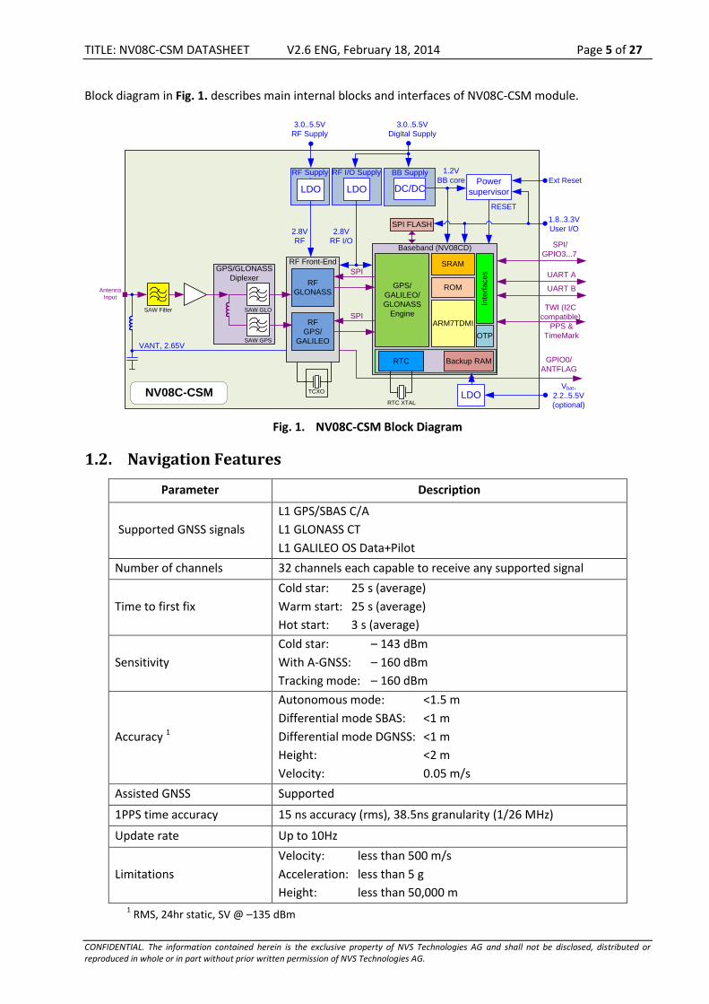
Block diagram in Fig. 1. describes main internal blocks and interfaces of NV08C-CSM module.
RF Supply
LDO
1.2V
BB core
1.8..3.3V
User I/O
3.0..5.5V
RF Supply
Ext Reset
2.8V
RF
NV08C-CSMVbat,
2.2..5.5V
(optional)
Baseband (NV08CD)
SRAM
ROM
ARM7TDMI
GPS/
GALILEO/
GLONASS
Engine
Backup RAMRTC
Inte
rfa
ce
s
OTP
RF Front-End
TCXO
RF
GLONASS
RF
GPS/
GALILEO
SPI
SPI
RTC XTAL
UART A
SPI/
GPIO3...7
TWI (I2C
compatible)
PPS &
TimeMark
Antenna
Input
3.0..5.5V
Digital Supply
Power
supervisor
BB Supply
DC/DC
RESET
GPS/GLONASS
Diplexer
SAW GLO
SAW GPS
SAW Filter
SPI FLASH
UART B
LDO
VANT, 2.65V
GPIO0/
ANTFLAG
RF I/O Supply
LDO
2.8V
RF I/O
Fig. 1. NV08C-CSM Block Diagram
1.2. Navigation Features
Parameter Description
Supported GNSS signals
L1 GPS/SBAS C/A
L1 GLONASS СТ
L1 GALILEO OS Data+Pilot
Number of channels 32 channels each capable to receive any supported signal
Time to first fix
Cold star: 25 s (average)
Warm start: 25 s (average)
Hot start: 3 s (average)
Sensitivity
Cold star: – 143 dBm
With A-GNSS: – 160 dBm
Tracking mode: – 160 dBm
Accuracy 1
Autonomous mode: <1.5 m
Differential mode SBAS: <1 m
Differential mode DGNSS: <1 m
Height: <2 m
Velocity: 0.05 m/s
Assisted GNSS Supported
1PPS time accuracy 15 ns accuracy (rms), 38.5ns granularity (1/26 MHz)
Update rate Up to 10Hz
Limitations
Velocity: less than 500 m/s
Acceleration: less than 5 g
Height: less than 50,000 m 1 RMS, 24hr static, SV @ –135 dBm
TITLE: NV08C-CSM DATASHEET V2.6 ENG, February 18, 2014 Page 6 of 27
CONFIDENTIAL. The information contained herein is the exclusive property of NVS Technologies AG and shall not be disclosed, distributed or reproduced in whole or in part without prior written permission of NVS Technologies AG.
1.3. RF Functionalities
The NV08C-CSM requires an active antenna to be connected to the RF input. The 2.65V active antenna
supply voltage is available at the RF input as soon as an active antenna is connected and a current flow is
present (if IANTBIAS > 1.1mА). If the antenna current draw exceeds 57 mA, short circuit protection will
automatically block the supply voltage to the RF input pin.
Note – An external voltage source can be used to power the active antenna, however the short-circuit
protection will not operate.
The NV08C-CSM features a two-stage RF-filter circuit that provides high out-of-band interference
immunity. A front-end wideband GPS+GLONASS RF filter ensures more than 40dB suppression of far-field
interference, from sources such as GSM, WiFi, WiMAX, LTE and Bluetooth signal transmitters. The second
filter stage is located at the output of the GPS/GLONASS Diplexer on two separate RF channels, ensuring
high channel separation and additional out-of-band interference attenuation.
The parameters of the NV08C-CSM’s RF inputs are as shown in Table 1.
Table 1. RF Input Parameters
Active Antenna
1dB Compression Point +30 dBm
Input Return Loss -15 dB
Total Noise Figure of the analogue path at the RF input 6 dB
Note – Table 1 shows estimated values. The actual values may differ as a result of device qualification.
The GPS/GLONASS Diplexer’s output signals are further processed by two independent analogue ICs on
two separate receiver channels:
GPS/GALILEO/SBAS L1 (1575.42 MHz @ 4 MHz)
GLONASS L1 (1601.5 MHz @ 8 MHz)
On both channels the satellite signals are first down-converted to the IF band (at approximately 4 to 5
MHz), then filtered by Polyphase Filters. The GPS channel filter has a bandwidth of 4 MHz, and the
GLONASS channel has a bandwidth of 8 MHz. The signals then pass through a Variable Gain Amplifier
with Automatic Gain Control. The analogue ICs include 2-bit ADCs that convert the signals from analogue
to digital to be processed by the digital baseband IC.
Typically both input channels are enabled to simultaneously receive all available navigation signals.
However to save power, one of two channels may be disabled via software (“GPS Only” mode).
In order to facilitate fast acquisition of low level signals in poor reception areas, the NV08C-CSM contains
a 26 MHz frequency generator (TCXO) with high temperature stability (±0.5 ppm).
1.4. Environmental Data
Operating temperature: -40°C to +85°C
Maximum relative humidity: 98% at +40°С
1.5. Data Interfaces
Host data interface:
TITLE: NV08C-CSM DATASHEET V2.6 ENG, February 18, 2014 Page 7 of 27
CONFIDENTIAL. The information contained herein is the exclusive property of NVS Technologies AG and shall not be disclosed, distributed or reproduced in whole or in part without prior written permission of NVS Technologies AG.
Two UART (4,800 to 230,400 bit/s)
1PPS output/external synchronization pulse (input)
8 GPIO
One SPI*
One TWI (I2C compatible)*
* requires a non-standard firmware load
Supported protocols:
IEC61162-1 (NMEA 0183)
BINR (proprietary)
RTCM v.2.x (messages #1, #31)
Data update/output rate: 1, 2, 5, 10 Hz
1.6. Electrical Parameters
The NV08C-CSM device requires the following power supply voltages:
Digital I/O supply 1.8 to 3.3 V
Digital and RF supply 3.0 to 5.5 V
Backup memory and RTC clock 2.2 to 5.5 V
The maximum power consumption is as follows:
Continuous tracking mode:
- GPS only 120 mW*
- GNSS 180 mW*
Sleep mode:
- 100 µA* (All power supplies must be provided)
Backup mode:
- 4 µA @ 2.2 to 5.5 V (only RTC and Backup RAM supply)
* average value.
The Sleep Mode allows minimizing power consumption of NV08C device without turning off of all power
supplies. NV08C devices are sleeping in thin mode (no signal tracking and navigation supported). Refer to
chapter 3.3. Sleep Mode for additional details.
The Backup Mode is supported by an on-chip real-time clock and static RAM, in order to safe-keep true
time and other parameters, while the main power is turned off. This feature allows the receiver’s start-up
time (prior to receiving first valid navigation data) to be much shorter. To use the Backup Mode backup
voltage must be provided to the VBAT pin (see chapters below).
TITLE: NV08C-CSM DATASHEET V2.6 ENG, February 18, 2014 Page 8 of 27
CONFIDENTIAL. The information contained herein is the exclusive property of NVS Technologies AG and shall not be disclosed, distributed or reproduced in whole or in part without prior written permission of NVS Technologies AG.
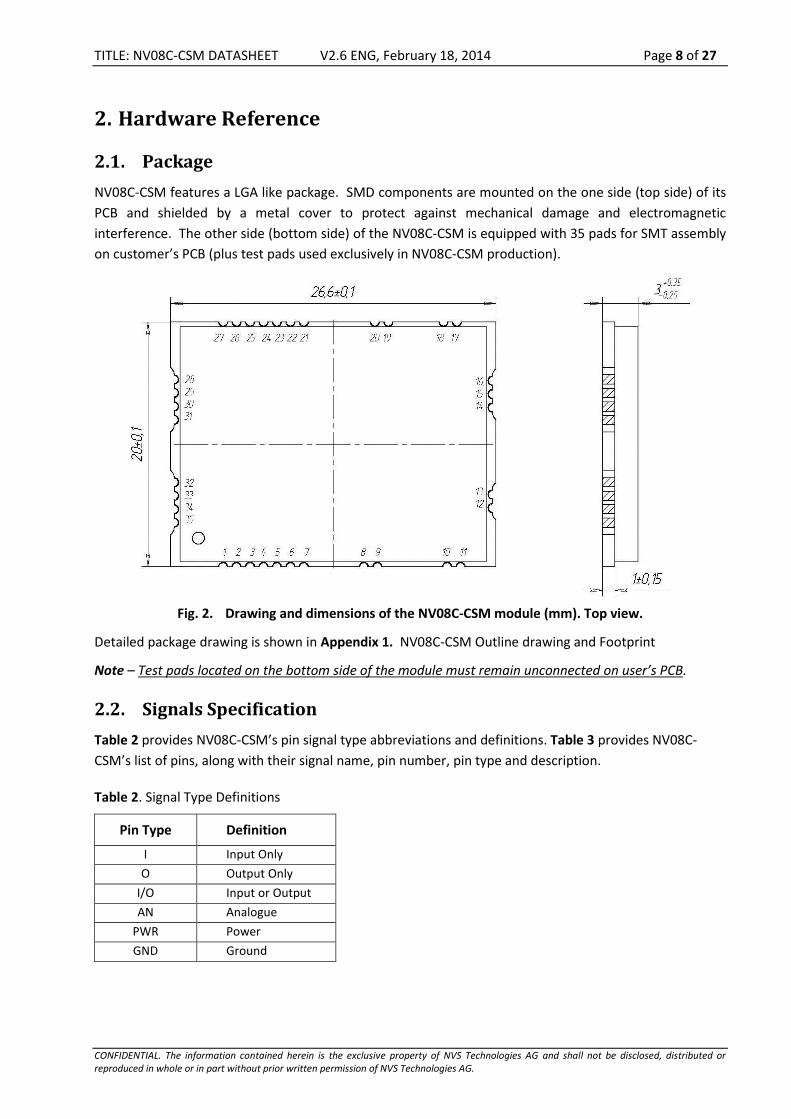
2. Hardware Reference
2.1. Package
NV08C-CSM features a LGA like package. SMD components are mounted on the one side (top side) of its
PCB and shielded by a metal cover to protect against mechanical damage and electromagnetic
interference. The other side (bottom side) of the NV08C-CSM is equipped with 35 pads for SMT assembly
on customer’s PCB (plus test pads used exclusively in NV08C-CSM production).
Fig. 2. Drawing and dimensions of the NV08C-CSM module (mm). Top view.
Detailed package drawing is shown in Appendix 1. NV08C-CSM Outline drawing and Footprint
Note – Test pads located on the bottom side of the module must remain unconnected on user’s PCB.
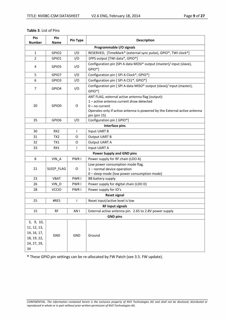
2.2. Signals Specification
Table 2 provides NV08C-CSM’s pin signal type abbreviations and definitions. Table 3 provides NV08C-
CSM’s list of pins, along with their signal name, pin number, pin type and description.
Table 2. Signal Type Definitions
Pin Type Definition
I Input Only
O Output Only
I/O Input or Output
AN Analogue
PWR Power
GND Ground
TITLE: NV08C-CSM DATASHEET V2.6 ENG, February 18, 2014 Page 9 of 27
CONFIDENTIAL. The information contained herein is the exclusive property of NVS Technologies AG and shall not be disclosed, distributed or reproduced in whole or in part without prior written permission of NVS Technologies AG.
Table 3. List of Pins
Pin Number
Pin Name
Pin Type Description
Programmable I/O signals
1 GPIO2 I/O RESERVED, [TimeMark* (external sync pulse), GPIO*, TWI clock*]
2 GPIO1 I/O 1PPS output [TWI data*, GPIO*]
4 GPIO5 I/O Configuration pin [SPI A data MOSI* output (master)/ input (slave),
GPIO*]
5 GPIO7 I/O Configuration pin [ SPI A Clock*, GPIO*]
6 GPIO3 I/O Configuration pin [ SPI A CS1*, GPIO*]
7 GPIO4 I/O Configuration pin [ SPI A data MISO* output (slave)/ input (master),
GPIO*]
20 GPIO0 O
ANT FLAG, external active antenna flag (output): 1 – active antenna current draw detected 0 – no current Operates only if active antenna is powered by the External active antenna pin (pin 15)
35 GPIO6 I/O Configuration pin [ GPIO*]
Interface pins
30 RX2 I Input UART B
31 TX2 O Output UART B
32 TX1 O Output UART A
33 RX1 I Input UART A
Power Supply and GND pins
8 VIN_A PWR I Power supply for RF chain (LDO A)
21 SLEEP_FLAG O Low power consumption mode flag. 1 – normal device operation 0 – sleep mode (low power consumption mode)
23 VBAT PWR I BB battery supply
26 VIN_D PWR I Power supply for digital chain (LDO D)
28 VCCIO PWR I Power supply for IO’s
Reset signal
25 #RES I Reset input/active level is low
RF input signals
15 RF AN I External active antenna pin. 2.65 to 2.8V power supply
GND pins
3, 9, 10,
11, 12, 13,
14, 16, 17,
18, 19, 22,
24, 27, 29,
34
GND GND Ground
* These GPIO pin settings can be re-allocated by FW Patch (see 3.5. FW update).
TITLE: NV08C-CSM DATASHEET V2.6 ENG, February 18, 2014 Page 10 of 27
CONFIDENTIAL. The information contained herein is the exclusive property of NVS Technologies AG and shall not be disclosed, distributed or reproduced in whole or in part without prior written permission of NVS Technologies AG.
2.3. Electrical Specification
2.3.1. Absolute Maximum Ratings
Table 4 provides NV08C-CSM’s absolute maximum (stress) ratings. Operation at or beyond these
maximum ratings might cause permanent damage to the device.
Table 4. Absolute Maximum Ratings
Symbol Parameter Minimum Maximum Unit Ts Storage Ambient Temperature -55 125 °C
VIN_A Supply Voltage for RF chain (LDO A) -0.3 6 V
VIN_D Supply Voltage for digital chain (LDO D)
-0.3 6 V
VCCIO Baseband IO Supply Voltage -0.5 4.6 V
VBAT Baseband Battery Supply Voltage -0.3 6 V
PRF RF_IN Signal Power 10 dBm
VIO GPIO7 – GPIO0, #RES (RESET)
Voltage -0.5 VCCIO +0.5 (<4.6) V
2.3.2. Recommended Operating Conditions
Recommended operating conditions guarantee correct device operation.
As long as the device is used within these ranges, electrical DC and AC characteristics are guaranteed.
2.3.2.1. Ambient Temperature
Table 5. Operating Ambient Temperature
Symbol Parameter Minimum Maximum Unit TA Operating Ambient Temperature -40 +85 °C
2.3.2.2. Power Supply Voltage
Table 6. Power Supply Voltage
Symbol Parameter Minimum Typical Maximum Unit VIN_A Supply Voltage for RF chain (LDO A) 3.0 3.3 5.5 V
VIN_D Supply Voltage for digital chain (LDO D) 3.0 3.3 5.5 V
VCCIO Baseband IO Supply Voltage 1.65 1.8/2.5/3.3 3.6 V
VBAT Baseband Battery Supply Voltage 2.2 3.3 5.5 V
Table 7. Antenna Power Supply
Symbol Parameter Minimum Typical Maximum Unit V_ANT Voltage active antenna 2.5 2.65 2.8 V
I_ANT Current consumption of active
antenna 1.1
1 57
2 mA
1 Minimum current for the built-in active antenna detector 2 Maximum active antenna current
TITLE: NV08C-CSM DATASHEET V2.6 ENG, February 18, 2014 Page 11 of 27
CONFIDENTIAL. The information contained herein is the exclusive property of NVS Technologies AG and shall not be disclosed, distributed or reproduced in whole or in part without prior written permission of NVS Technologies AG.
2.3.2.3. Input Voltage
Table 8. Input Voltage for GPIO7 – GPIO0
Symbol Parameter IO Power Supply
Voltage VCC_BBIO Minimum Maximum Unit
VIH High Level Input
Voltage
3.3V 2.0 VCCIO + 0.3 V
2.5V 1.7 VCCIO + 0.3 V
1.8V 0.65 x VCC_BBIO VCCIO + 0.3 V
VIL Low Level Input
Voltage
3.3V -0.3 0.8 V
2.5V -0.3 0.7 V
1.8V -0.3 0.35 x VCCIO V
Table 9. Input Voltage for #RES (RESET)
Symbol Parameter IO Power Supply
Voltage VCC_BBIO Minimum Maximum Unit
VIH High Level Input
Voltage
3.3V 2.1 VCCIO + 0.3
V 2.5V 1.7 VCCIO + 0.3
1.8V 0.7 x VCCIO VCCIO + 0.3
1.2V 0.7 x VCCIO VCCIO + 0.3
VIL Low Level Input
Voltage
3.3V -0.3 0.7
V 2.5V -0.3 0.7
1.8V -0.3 0.3 x VCCIO
1.2V -0.3 0.3 x VCCIO
The NV08C-CSM’s inputs and outputs are either pulled-up or pulled-down (internally) as described in
Table 10. Refer to Table 11 for resistor values (BB I/O cells).
Table 10. I/O State after RESET
I/O Pull UP/ Pull Down
after RESET GPIO7 PU
GPIO6 PU
GPIO5 PD
GPIO4 PD
GPIO3 PD
GPIO2 PU
GPIO1 PU
GPIO0 PU
UARTA TX PU
UARTA RX PD
UARTB TX PU
UARTB RX PD
TITLE: NV08C-CSM DATASHEET V2.6 ENG, February 18, 2014 Page 12 of 27
CONFIDENTIAL. The information contained herein is the exclusive property of NVS Technologies AG and shall not be disclosed, distributed or reproduced in whole or in part without prior written permission of NVS Technologies AG.
Table 11. Pull-up and Pull-down Resistors
I/O cell resistor Supply voltage Min Nominal Max
Pull-Up resistor, kOhm
VCCIO = 3.3V 28 43 86
VCCIO = 2.5V 37 58 99
VCCIO = 1.8V 53 97 175
Pull-Down resistor, kOhm
VCCIO = 3.3V 25 41 95
VCCIO = 2.5V 33 59 113
VCCIO = 1.8V 52 107 212
2.3.2.4. DC Characteristics
Table 12. DC Characteristics
Symbol Parameter IO Power Supply
Voltage VCC_BBIO Conditions Minimum Maximum Unit
VOH
High Level
Output
Voltage
3.3V IOH = -100uA VCCIO -0.2 -
V
IOH = -4mA VCCIO -0.4 -
2.5V IOH = -100uA VCCIO -0.2 -
IOH = -4mA VCCIO -0.45 -
1.8V IOH = -100uA VCCIO -0.2 -
IOH = -3mA VCCIO -0.45 -
VOL
Low Level
Output
Voltage
3.3V IOL = 100uA - 0.2
V
IOL = 4mA - 0.35
2.5V IOL = 100uA - 0.2
IOL = 4mA - 0.4
1.8V IOL = 100uA - 0.2
IOL = 3mA - 0.45
IL Input Leak - - ±4 uA
2.3.3. Power Consumption
Table 13. Current Consumptions
Symbol Parameter Minimum Typical Maximum Unit
IVIN_A Total supply current through pin
VIN_A1
20 30 mA
IVIN_D BB Core Supply Current VIN_D 25 40 mA
IVBAT BB Battery Supply Current2 0.1 mA
IVBAT_STBY BB Battery Supply Standby
Current 4 uA
IV_IO BB IO Supply Current3 40 mA
IV_IO_STBY BB IO Supply Standby Current4 20 uA
Notes:
1. Without active antenna current
2. BRAM access rate less than 1M/s
3. Load dependent, maximum current 4mA per digital IO
4. RF portion switched off, module in power saving mode
TITLE: NV08C-CSM DATASHEET V2.6 ENG, February 18, 2014 Page 13 of 27
CONFIDENTIAL. The information contained herein is the exclusive property of NVS Technologies AG and shall not be disclosed, distributed or reproduced in whole or in part without prior written permission of NVS Technologies AG.
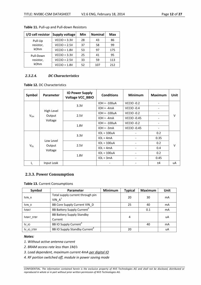
2.4. Hardware Integration Guide
2.4.1. Power Supply
2.4.1.1. Wiring NV08C-CSM to an External Power Supply
Fig. 3 Provides the NV08C-CSM’s power connection diagram
LDO D
LDO AIN
EN
OUT
IN
EN
OUT
RF FE
VRF I/O (2.8V)
VRF (2.8V)
BB
VI/O (1.8...3.3V)
Vbat (1.2V)
Vcore (1.2V)
VRF I/O (2.8V)
VCCIO
VBAT
VIN_D
VIN_A
NV08C-CSM
LDO_SHDN
DC/DCIN OUT
LDOIN OUT
Fig. 3. NV08C-CSM Power Connection Diagram
Four supply inputs for maximum system integration flexibility:
1. RF-core power supply (LDO A) .............................................. VIN_A, 3.0 to 5.5 V
2. Digital core power supply (LDO D) ........................................ VIN_D, 3.0 to 5.5 V
3. Backup power supply ............................................................ VBAT, 2.2 to 5.5 V
4. I/O power supply ................................................................... VCCIO, 1.8 to 3.3 V
Note – Supply voltages shown above are nominal values. Please refer to Table 6 for maximum upper and
lower limits.
The RF front-end is powered by the integrated LDO A and LDO D low-dropout linear regulators. The LDO A
provides a clean analogue voltage supply to the RF section, and the LDO D provides a regulated voltage
supply to the digital circuitry. The input power supply for the LDO A and LDO D (VIN_A and VIN_D) has a
voltage range of 3.0 to 5.5V. The digital baseband (BB) uses three types of voltages: 1.2V as the core
voltage (supplied by integrated DC/DC converter), IO voltage (VССIO, 1.8…3.3V) and a backup supply 1.2V
for a Real-Time Clock and backup RAM (supplied by integrated LDO). The Backup power option (VBAT,
2.2…5.5V) must be powered for “hot start” and “warm start” functions. If not required VBAT must be
connected to VIN_D.
In User systems power may be provided to the NV08C-CSM in a number of different ways depending on
specific design requirements and voltage supply availability. Some of the most common cases are
described in the following sections.
TITLE: NV08C-CSM DATASHEET V2.6 ENG, February 18, 2014 Page 14 of 27
CONFIDENTIAL. The information contained herein is the exclusive property of NVS Technologies AG and shall not be disclosed, distributed or reproduced in whole or in part without prior written permission of NVS Technologies AG.
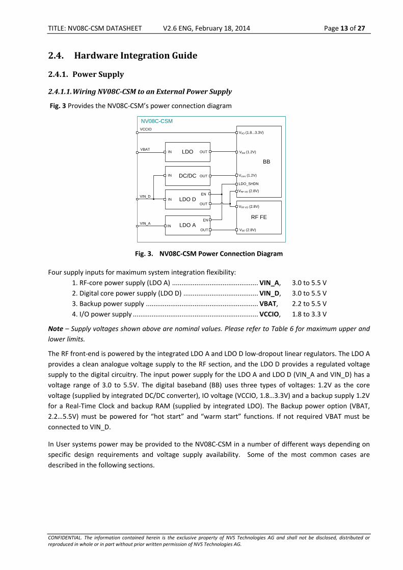
2.4.1.2. Single voltage power supply
The external power supply V_IN must be connected to the VIN_A, VIN_D, VCCIO and VBAT pins as follows.
Table 14. External Power Supply Voltage Range
Power Supply Voltage (V)
Min Max
V_IN 3.0 3.6
LDO D
LDO AIN
EN
OUT
IN
EN
OUT
RF FE
VRF I/O (2.8V)
VRF (2.85V)
BB
VI/O (1.8...3.3V)
Vbat (1.2V)
Vcore (1.2V)
VRF I/O (2.8V)
VCCIO
VBAT
VIN_D
VIN_A
NV08C-CSM
LDO_SHDN
DC/DCIN OUT
LDOIN OUT
V_IN
Fig. 4. Power connection to a single voltage
power supply
2.4.1.3. External power supply for digital I/Os
Often in User systems, the digital IO signal voltage range differs from the NV08C-CSM’s V_IN. To allow
for uniform digital IO voltage levels in the NV08C-CSM as in the rest of the User’s system, the User
system’s IO voltage supply must be connected to VCCIO instead of V_IN.
Table 15. External Power Supply Voltage Range
Power Supply Voltage (V)
Min Max
V_IN 3.0 5.5
V_IO 1.65 3.6
LDO D
LDO AIN
EN
OUT
IN
EN
OUT
RF FE
VRF I/O (2.8V)
VRF (2.85V)
BB
VI/O (1.8...3.3V)
Vbat (1.2V)
Vcore (1.2V)
VRF I/O (2.8V)
VCCIO
VBAT
VIN_D
VIN_A
NV08C-CSM
LDO_SHDN
DC/DCIN OUT
LDOIN OUT
V_IN
V_IO
Fig. 5. Power connection to digital I/Os with an
external power supply
TITLE: NV08C-CSM DATASHEET V2.6 ENG, February 18, 2014 Page 15 of 27
CONFIDENTIAL. The information contained herein is the exclusive property of NVS Technologies AG and shall not be disclosed, distributed or reproduced in whole or in part without prior written permission of NVS Technologies AG.
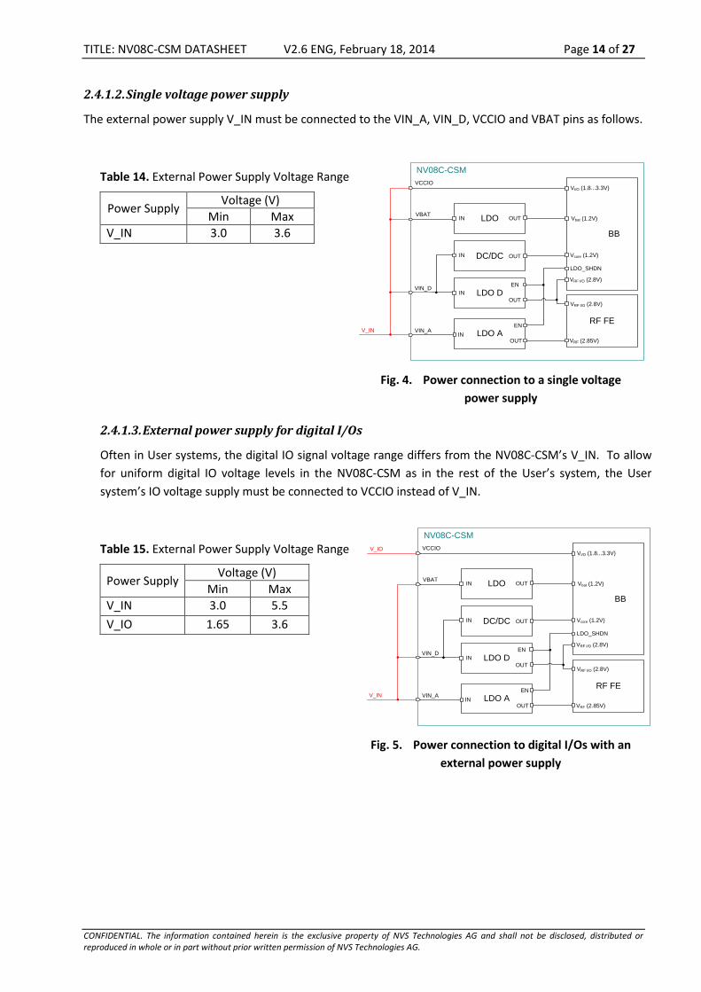
2.4.1.4. Backup Power Supply
The baseband contains a backup Power Island, which is powered via the pin VBAT. The Power Island
contains a Real-Time Clock and backup RAM. If a backup power supply is implemented in the User’s
system, the VBAT must be powered by the backup supply, so that if the main power supply goes off, the
RTC and backup RAM remain powered, hence providing necessary data for faster receiver starts on
power-on (warm and hot starts).
Fig. 6 describes the power connections for when the baseband core, backup and IOs supply voltages are
provided by the User’s system.
Table 16. Voltages of External Power Supply
Power Supply Voltage (V)
Min Max
V_IN1 3.0 3.6
V_IN2 3.0 5.5
V_IO2 1.65 3.6
V_BU 2.2 5.5
Notes: 1 For when VССIO connected to V_IN.
2 For when VССIO connected to V_IO.
LDO D
LDO AIN
EN
OUT
IN
EN
OUT
RF FE
VRF I/O (2.8V)
VRF (2.85V)
BB
VI/O (1.8...3.3V)
Vbat (1.2V)
Vcore (1.2V)
VRF I/O (2.8V)
VCCIO
VBAT
VIN_D
VIN_A
NV08C-CSM
LDO_SHDN
DC/DCIN OUT
LDOIN OUT
V_IN
V_IO
V_BU
Fig. 6. Power connections to external power
supplies for baseband core, IOs and backup
2.4.1.5. Decoupling Capacitors
All necessary decoupling capacitors are integrated in the NV08C-CSM. Nevertheless, in order to
minimize the effect of power supply noise on reception of signals it is recommended to;
Separate power supplies VIN_A and VIN_D either by means of separate power sources
or by using inductive isolation.
Provide an additional capacitor 22pF (0201, NPO or X7R) as close to pin VIN_A as
possible.
As an option power supply inputs may be equipped with capacitors as shown in the Table 17.
Table 17. Power Supply Capacitors (optional)
Pin Recommended
Capacitors Note
VIN_A 1 uF ceramic Optional
VIN_D 1 uF ceramic Optional
VССIO 1 uF ceramic Optional
VBAT 1 uF ceramic Optional
TITLE: NV08C-CSM DATASHEET V2.6 ENG, February 18, 2014 Page 16 of 27
CONFIDENTIAL. The information contained herein is the exclusive property of NVS Technologies AG and shall not be disclosed, distributed or reproduced in whole or in part without prior written permission of NVS Technologies AG.
2.4.1.6. Typical Power Consumption
Table 18 shows average power consumption of the NV08C-CSM in continuous tracking. Power
consumption via VCCIO is typically lower than the consumption of the RF, front end and baseband core.
Table 18. Average Power Consumption of the NV08C-CSM in Time-to-Time-Fix Mode
Mode Power supply options
Tracking & navigation, GPS only < 120 mW
Tracking & navigation, GNSS < 180 mW
2.4.2. Reset
NV08C-CSM’s Input signal #RES (RESET, pin # 25) can be driven by the User’s system to force the reset of
the digital portion of the device. To reset the device the User’s system should provide a pulse to the
#Res input pad as specified below:
Voltage level – less than 0.3хVCCIO
The pulse length – no less than 1 ms
After the signal is applied (#RES signal level goes from low to high) the integrated power supervisor
holds the device in reset mode for at least 140 ms. Please refer Table 9 for Reset signal level
requirements.
2.4.3. 1PPS Output
1PPS output is present at the GPIO1 pin. By default 1PPS signal is generated permanently and
independently of a valid position fix whether available or not. If a valid position fix is not available, the
1PPS signal will be generated each second as per the internal hardware’s defined time scale. If a valid
position fix is available, the 1PPS signal refers to a user defined time standard (UTC by default). If
required the 1PPS output can be set to operate only when a valid position fix is available.
1PPS signal parameters:
- Voltage level 1.8…3.3V (depends of VCCIO; CMOS) - Output frequency 1 Hz - True time Refer to the pulse rising (default) or the falling edge - Pulse duration 38.5 ns to 2.5 ms (1 ms by default) - Refers to UTC (default), GPS, GLONASS or UTC SU time standard
- 1PPS accuracy 15 ns (antenna cable delay to be compensated) - 1PPS granularity 38.5 ns (26 MHz TCXO referenced)
The rising (or falling) edge shift is relative to the defined time-standard, and is available in the NMEA $POUTC and BINR 72h message (generated within 20 ms after the 1PPS pulse).
2.4.4. Active Antenna connection
The NV08C-CSM requires an external active antenna. A 2.65V voltage supply is provided at the RF input
to power the active antenna. If the antenna current draw exceeds 57 mA, the RF input supply voltage is
automatically blocked by short-circuit protection.
TITLE: NV08C-CSM DATASHEET V2.6 ENG, February 18, 2014 Page 17 of 27
CONFIDENTIAL. The information contained herein is the exclusive property of NVS Technologies AG and shall not be disclosed, distributed or reproduced in whole or in part without prior written permission of NVS Technologies AG.
It is very important to choose a proper antenna. An active antenna with too much LNA gain and wide
passband may reduce the quality of signal reception due to possible in-band and out-of-band
interference. As well an active antenna with too little gain or with high cable attenuation may decrease
the receiver’s sensitivity.
Recommended active antenna parameters are as follows:
GPS/GLONASS L1, bandwidth 35 MHz @ fc = 1590 MHz
Gain including cable attenuation 20-30 dB
Antenna noise figure <2 dB
Out-of-band signal attenuation: at least 35dB @ fc ± 70 MHz.
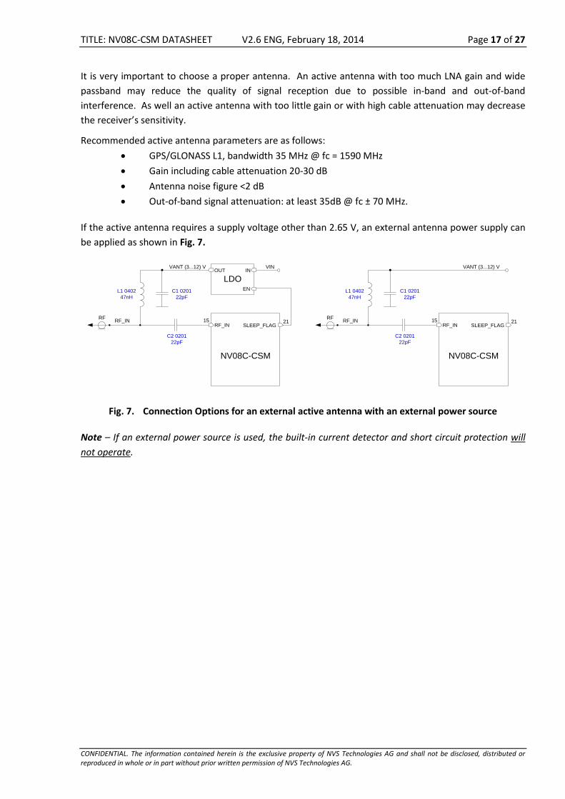
If the active antenna requires a supply voltage other than 2.65 V, an external antenna power supply can
be applied as shown in Fig. 7.
NV08C-CSM
RF_INRF_IN
15
L1 0402
47nH
VANT (3...12) V
RF
C1 0201
22pF
LDOOUT IN
EN
SLEEP_FLAG
VIN
C2 0201
22pF
21
NV08C-CSM
RF_INRF_IN
15
L1 0402
47nH
VANT (3...12) V
RF
C1 0201
22pF
SLEEP_FLAG
C2 0201
22pF
21
Fig. 7. Connection Options for an external active antenna with an external power source
Note – If an external power source is used, the built-in current detector and short circuit protection will
not operate.
TITLE: NV08C-CSM DATASHEET V2.6 ENG, February 18, 2014 Page 18 of 27
CONFIDENTIAL. The information contained herein is the exclusive property of NVS Technologies AG and shall not be disclosed, distributed or reproduced in whole or in part without prior written permission of NVS Technologies AG.
2.4.5. Digital IO Interfaces
The NV08C-CSM provides two UART interfaces, one SPI interface* (for FLASH/EEPROM connection), one
two-wire interface (I2C compatible)* and GPIO interfaces.
* - these options are not available by default and are available only with a specific FW Patch (see
chapter 3.5. FW update).
IO interfaces in NV08C-CSM are connected to external devices via 8 pins (GPIO7 – GPIO0).
Table 19. Default Configuration of pins P7 – P0
Pin Status after RESET Description
GPIO7 GPIO7
Configuration pads (See Table 20)
GPIO6 GPIO6
GPIO5 GPIO5
GPIO4 GPIO4
GPIO3 GPIO3
GPIO2 TimeMark Currently reserved. The PIO can be re-allocated as External time
synchronization input by FW Patch.
GPIO1 PPS 1 PPS output
GPIO0 ANTFLAG
Active antenna current trigger:
"1" - Active antenna connected (current > 1.1mА)
"0" - no load.
Note: The pads that are not used by the User's system as UART, 1PPS or TimeMark can be programmed as GPIO.
Table 20. Configuration Settings
GPIO
(I/O number) Function PIO value Description
GPIO7 (5) Settings saving in
BRAM
GPIO7 = 1 (default) Save all settings
GPIO7 = 0 Do not save settings
GPIO6 (35) Allows FW Patch
download via SPI A
GPIO6 = 1 (default) GPIO7, GPIO5, GPIO4, GPIO3 used only for
configuration purpose
GPIO6 = 0
GPIO7, GPIO5, GPIO4, GPIO3 are
configured as SPI and will be used for FW
Patch download from external SPI-FLASH
GPIO5 (4)
GPIO4 (7)
GPIO3 (6)
UART port
configuration
GPIO5 = 0 (default)
GPIO4 = 0 (default)
GPIO3 = 0 (default)
UART A – 115200 NMEA (GGA/1, RMC/1,
GSV/1, GSA/1, RZD/1, GBS/10*)
UART B – 115200 BINR
GPIO5 = 0
GPIO4 = 0
GPIO3 = 1
UART A – 4800 NMEA (GGA/1, RMC/1,
GSV/1, GSA/1, RZD/1, GBS/10*)
UART B – 19200 BINR
GPIO5 = 0
GPIO4 = 1
GPIO3 = 0
UART A – 9600 NMEA (GGA/1, RMC/1,
GSV/1, GSA/1, RZD/1, GBS/10*)
UART B – 19200 BINR
TITLE: NV08C-CSM DATASHEET V2.6 ENG, February 18, 2014 Page 19 of 27
CONFIDENTIAL. The information contained herein is the exclusive property of NVS Technologies AG and shall not be disclosed, distributed or reproduced in whole or in part without prior written permission of NVS Technologies AG.
GPIO
(I/O number) Function PIO value Description
GPIO5 = 0
GPIO4 = 1
GPIO3 = 1
UART A – 19200 NMEA (GGA/1, RMC/1,
GSV/1, GSA/1, RZD/1, GBS/10*)
UART B – 57600 BINR
GPIO5 = 1
GPIO4 = 0
GPIO3 = 0
UART A – 38400 NMEA (GGA/1, RMC/1,
GSV/1, GSA/1, RZD/1, GBS/10*)
UART B – 38400 BINR
GPIO5 = 1
GPIO4 = 0
GPIO3 = 1
UART A – 38400 NMEA (GNS/1, RMC/1,
GSA/1, GBS/10, GSV/10,
DTM/30*)
UART B – 4800 RТСМ
GPIO5 = 1
GPIO4 = 1
GPIO3 = 0
UART A – 4800 NMEA (GNS/1, RMC/1,
GSA/1, GBS/10, GSV/10,
DTM/30*)
UART B – 4800 RТСМ
GPIO5 = 1
GPIO4 = 1
GPIO3 = 1
UART A – 57600 NMEA (GGA/1, RMC/1,
GSV/1, GSA/1, RZD/1, GBS/10*)
UART B – 57600 BINR
* - default NMEA messages and time interval
Note – By default the NMEA output is enabled (GNS/1s, RMC/1s, GSA/1s, GBS/10s, GSV/10s, DTM/30s
messages) and the BINR output is disabled. To enable the BINR output a query message must be sent
(see Protocol Specification).
2.4.6. Backup Power Supply VBAT
If an independent VBAT voltage is applied, the NV08C-CSM module can store (in its BRAM) navigation
parameters (almanac, ephemeris, last calculated coordinates etc.), as well as user defined settings (ports
and receiver configuration settings).
When navigation parameters are stored, the module is able to provide warm or hot starts (depending
on its switch-off time and available navigation data).
The user defined settings mode is defined by the GPIO7’s signal level (“1” – saved, “0” – not saved). By
default the GPIO7 is pulled-up (“1”).
If no VBAT voltage is applied to the module, all data saved in the BRAM will be erased when the module
is powered off.
TITLE: NV08C-CSM DATASHEET V2.6 ENG, February 18, 2014 Page 20 of 27
CONFIDENTIAL. The information contained herein is the exclusive property of NVS Technologies AG and shall not be disclosed, distributed or reproduced in whole or in part without prior written permission of NVS Technologies AG.
3. Software and Protocols Reference
3.1. Data Protocol and Configuration
The NV08C-CSM can interface to an external host-processor using the following protocols:
BINR (proprietary binary protocol)
NMEA 0183
RTCM v2.x (messages #1, #31)
Note – See description of communication messages in the Protocol Specification document.
By default, the module’s interfaces are configured as follows:
UART A: Protocol NMEA, 115,200 bps
UART B: Protocol BINR, 115,200 bps
Note – Both ports can be configured to receive differential correctional data in RTCM format. Even in
this configuration, it is still possible to control the module by adding NMEA-commands to the RTCM
stream, since the NV08C-CSM’s SW is able to sort out data types. In order to use this option the port
must first be activated by a $PORZA message to accept the RTCM data, then the NMEA message output
stream can be defined by a $PORZB message. (Refer to the Protocol Specification document for $PORZA
and $PORZB messages description.)
Other NV08C-CSM default settings:
navigation mode: GPS and GLONASS
SBAS data: accounted automatically
RAIM: automatic
Assisted data: accounted automatically
navigation data update rate: 1 Hz
NMEA messages: GSA, RMC, GGA, GSV, GBS
Standard settings can be changed by using the following means:
pre-set configuration codes to assign certain specific GPIO inputs (refer to Table 20 GPIO7 –
GPIO3 settings)
NMEA/BINR protocol commands via UART А/В ports
3.2. Low Power Battery Mode
The NV08C-CSM has a sophisticated system to reduce its power consumption. The supported power
conservation methods are as follows:
automatic clock gating of unused subsystems (such as the fast search function, unused
correlation channels, and interface blocks)
option to completely turn-off the power to one of the two analogue channels
3.3. Sleep Mode
If navigation function is not required power consumption can be minimized by switching the NV08C-
CSM device to Sleep mode. A Host system can activate the Sleep mode by sending the
TITLE: NV08C-CSM DATASHEET V2.6 ENG, February 18, 2014 Page 21 of 27
CONFIDENTIAL. The information contained herein is the exclusive property of NVS Technologies AG and shall not be disclosed, distributed or reproduced in whole or in part without prior written permission of NVS Technologies AG.
$POPWR,1111*66<CR><LF> NMEA command. When NV08C-CSM enters the Sleep Mode SLEEP_FLAG
pin goes to LOW state, Both RF-chains and TCXO are turned off and BB ASIC consumes minimal power.
Note: The time interval required for NV08C-CSM device to enter Sleep mode depends on the
communication baud rate since NMEA commands should be received and decoded. After commands
decoding a minimum of 10 ms is required for the device to safely enter Sleep mode.
The NV08C-CSM device wakes up when the Host System sends any command via UART port.
Note: The NV08C-CSM device is sensitive to the falling edge of UART RX signals. A minimum of 10 ms
after detecting a falling edge is required to switch the device from IDLE to normal operation mode,
otherwise the first sent command cannot be properly decoded. Therefore a timeout is required prior to
sending of the next control command by the Host System.
3.4. Assisted GNSS
The NV08C-CSM supports the use of external assisted data functions for applications that require quick-
navigation on power-up. Assisted data is provided by the User’s system via wireless means such as GSM
or CDMA, or by the Internet, and loaded onto the module via the BINR protocol. Assisted data comes in
a compact format (binary data file) and is ready for download on supported sites.
3.5. FW update
To download Patch Code (FW) via a UART interface (Fig. 8) the following command must be sent to the
NV08C-CSM:
- for NMEA protocol: $POPRL,R*2F\r\n
- for BINR protocol: 0х10 0х01 0х52 0х45 0х4С 0x4F 0x41 0x44 0x5F 0x52 0x10 0x03
By receiving the command the NV08C-CSM shifts into programming mode and starts the output of
character 0x43 (in ASCII – character "C") to UART TX. In response the User's system must download
Patch Code in the form of sequence of bytes (provided as a binary file) by means of X-modem-CRC
protocol. As soon as the binary file is completely downloaded the module stores the Patch Code in its
non-volatile memory and restarts.
NVS Technologies can support application specific requirements. Contact NVS’ Technical Support for
customisation of standard functionalities.
The PatchWriter (Firmware downloading tool) and the latest revision of the Firmware Patch (FW) are
available at www.nvs-gnss.com.
NV08C-CSM
TX
RX
External
Device
RX
TX
UA
RT
A /
UA
RT
B
Fig. 8. Connecting the NV08C-CSM to an external device to download Patch Code (FW)
TITLE: NV08C-CSM DATASHEET V2.6 ENG, February 18, 2014 Page 22 of 27
CONFIDENTIAL. The information contained herein is the exclusive property of NVS Technologies AG and shall not be disclosed, distributed or reproduced in whole or in part without prior written permission of NVS Technologies AG.
FW updating via Patch downloads can be performed for an unlimited number of times (within the FLASH
memory specification – typically up to 100K writing cycles). First the old FW Patch is erased from
memory then the new FW Patch is stored to memory. Any FW Patch version corresponding to the
MaskROM version can be downloaded to the NV08C-CSM. (For example - the newer version of the Patch
can be downgraded by downloading an older version.) However if a Patch version being downloaded
doesn’t correspond to the module MaskROM version, the Patch will not be stored in the FLASH memory.
FW versions 02.xx and 01.xx are only compatible with NV08C-CSM v.3.x Hardware. FW 02.xx is used for
official FW releases (recommended for all users). FW 01.xx supposes a customization of official FW
version for specific user demands.
IMPORTANT NOTE: Don’t load FW 04.xx or 03.xx into NV08C-CSM v.3.x. Not following this prescription
might lead to unrecoverable device malfunction.
FW version 04.xx and 03.xx are only compatible with NV08C-CSM v.4.x Hardware. FW 04.xx is used for
official FW releases (recommended for all users). FW 03.xx supposes a customization of official FW
version for specific user demands.
IMPORTANT NOTE: don’t load FW 02.xx or 01.xx into NV08C-CSM v.4.x. Not following this prescription
might lead to unrecoverable device malfunction.
Caution – Storing of the Patch to the FLASH memory will only begin when transmission of the Patch to
the module is fully completed (this will require a few seconds). During this process the NV08C-CSM
must not be powered-off and RESET must not be applied. Turning off or resetting while doing a Patch
download might lead to a malfunction of the NV08C-CSM and recovery can only be done by the factory.
3.6. Dead Reckoning Option
The NV08C-CSM features a Dead Reckoning function which provides seamless navigation even when
satellite signals are partially blocked or completely unavailable (example: tree canopy, urban canyons,
covered parking, tunnels, mountains etc.). The NV08C-CSM’s Dead Reckoning algorithm is intended for
automotive applications that provide two wheel-pulse signals from a single-axle.
Note – the User’s system must match the signal levels to the NV08C-CSM’s GPIO inputs.
Please contact NVS’ Technical Support to obtain Dead Reckoning FW option support.
TITLE: NV08C-CSM DATASHEET V2.6 ENG, February 18, 2014 Page 23 of 27
CONFIDENTIAL. The information contained herein is the exclusive property of NVS Technologies AG and shall not be disclosed, distributed or reproduced in whole or in part without prior written permission of NVS Technologies AG.
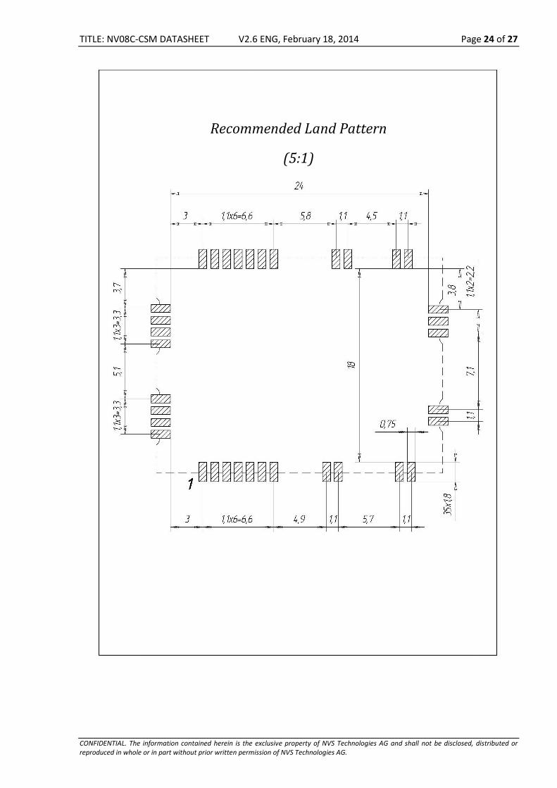
Appendix 1. NV08C-CSM Outline drawing and Footprint
TITLE: NV08C-CSM DATASHEET V2.6 ENG, February 18, 2014 Page 24 of 27
CONFIDENTIAL. The information contained herein is the exclusive property of NVS Technologies AG and shall not be disclosed, distributed or reproduced in whole or in part without prior written permission of NVS Technologies AG.
Recommended Land Pattern
(5:1)
TITLE: NV08C-CSM DATASHEET V2.6 ENG, February 18, 2014 Page 25 of 27
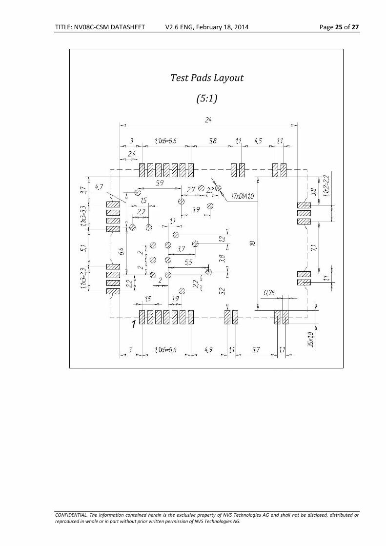
CONFIDENTIAL. The information contained herein is the exclusive property of NVS Technologies AG and shall not be disclosed, distributed or reproduced in whole or in part without prior written permission of NVS Technologies AG.
Test Pads Layout
(5:1)
TITLE: NV08C-CSM DATASHEET V2.6 ENG, February 18, 2014 Page 26 of 27
CONFIDENTIAL. The information contained herein is the exclusive property of NVS Technologies AG and shall not be disclosed, distributed or reproduced in whole or in part without prior written permission of NVS Technologies AG.
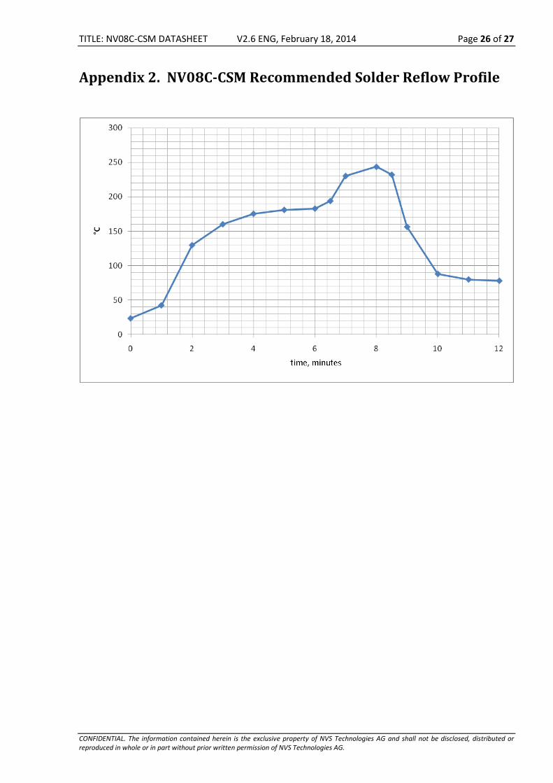
Appendix 2. NV08C-CSM Recommended Solder Reflow Profile
TITLE: NV08C-CSM DATASHEET V2.6 ENG, February 18, 2014 Page 27 of 27
CONFIDENTIAL. The information contained herein is the exclusive property of NVS Technologies AG and shall not be disclosed, distributed or reproduced in whole or in part without prior written permission of NVS Technologies AG.
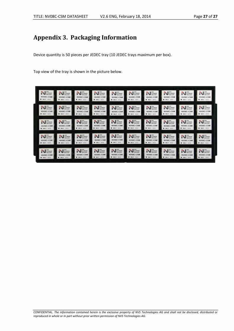
Appendix 3. Packaging Information
Device quantity is 50 pieces per JEDEC tray (10 JEDEC trays maximum per box).
Top view of the tray is shown in the picture below.