Embed Size (px)
DESCRIPTION
notas PIC
Citation preview
AN1451Glitch-Free Design Using the Configurable Logic Cell (CLC)
INTRODUCTION
One of the challenges that digital designers run intofrequently involves getting rid of glitches in their design.This is typically accounted for by ensuring there isadequate set-up and hold time when data is latched.
A ‘glitch’ is a signal which does not remain active for afull clock period. If a signal with a glitch feeds the clockline of numerous latches, some of the latches may getupdated, while others may not. This is clearly asituation that designers want to avoid.
It should also be noted that propagation delay varieswith temperature, therefore, a design which does notproduce glitches during development may produceglitches under different conditions.
The addition of the Configurable Logic Cell (CLC) to theMicrochip set of peripherals allows end-users to essen-tially “design” a simple peripheral that can interfacewith the PIC® microcontroller. With the ability to drivesignals into the PIC device that can cause interruptsand increment counters, it is necessary to providesome instruction so that stable designs can be createdusing the CLC peripheral.
A PIC16F1509 was used for this example, and it usesthree of the four available CLC modules. The 4th CLCmodule is being used to route the internal FOSC signalto the RC4 pin, so that it can be viewed with a logicanalyzer. Other signals internal to the CLC (XORoutput, latch output) have been brought out on externalpins to provide greater visibility of how the applicationis functioning.
The block diagram (Figure 1) shows the asynchronousinput signal on RC3, with the CLC outputs feeding thelogic analyzer. The CLC3 signal is our glitch-free clocksignal and is being fed into the NCO1CLK pad.
FIGURE 1: GLITCH-FREE BLOCK DIAGRAM – BENCH SET-UP
In this example, we will create a high-speed counterwhich is used to increment the NCO register. The NCOwill increment as long as an external pulse signal ishigh. This creates a high-resolution, long-durationcounter, as the NCO counter is a 20-bit wide register. Itwill take approximately 16 instruction cycles (4 µs with16 MHz clock) for the data to be read and the counter toreset, so it is necessary to have at least 4 µs of low timebetween pulses. A falling edge interrupt flag on CLC2provides a signal that the pulse width measurement has
been completed. While the NCO register has beendesigned to be resistant to glitches on the clock input, itis still good design practice to have clean signalsfeeding into the NCO clock line.
Author: Stephen AllenMicrochip Technology Inc.
2012 Microchip Technology Inc. DS01451A-page 1

AN1451
The first design for this circuit does allow glitches topass in, and is a simple ‘AND’ of the pulse signal withthe system clock. Note how a spike on the clock iscreated when the pulse signal rises shortly before theclock falls (Figure 2).
FIGURE 2: LOGICAL ‘AND’ OF ASYNCHRONOUS PULSE AND SYSTEM CLOCK
We want to use the ‘AND’ function to clock the NCOwhen the pulse is high, but we would like to get rid ofthe glitches on the clock signal. In order to do this, itwould be ideal to create a pulse –> new signal thatwould only rise on the rising edge of the clock, and onlyfall on the falling edge of the clock. This new signal(CLC2OUT) can be AND’ed with the oscillator clock,and there will never be a glitch on the NCO clock signal.A simple state diagram (Figure 3) shows how this willwork.
FIGURE 3: STATE DIAGRAM FOR CLEAN TRANSITION
Asynchronous input signal
PIC® MCU internal oscillator
Clock signal with glitch
DS01451A-page 2 2012 Microchip Technology Inc.
AN1451
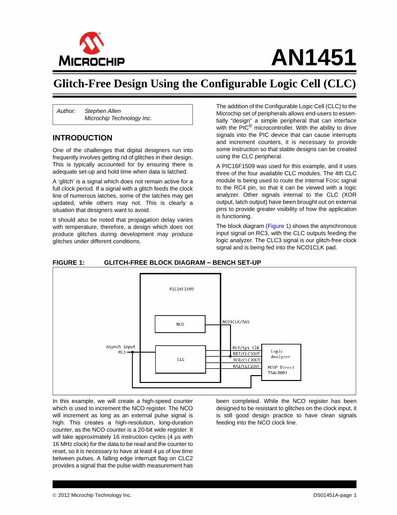
This state diagram can be implemented with a D flip-flopand an XOR gate. The XOR gate will have the functionof taking feedback from the D flip-flop and inverting theclock, so that it will trigger on the falling edge once the
flip-flop has been set. A schematic for this is shownbelow (Figure 4). This new signal (CLC2OUT) can beAND’ed with the oscillator clock, and there will never bea glitch on the NCO clock signal.
FIGURE 4: CREATING GLITCH-FREE CLOCK SIGNAL
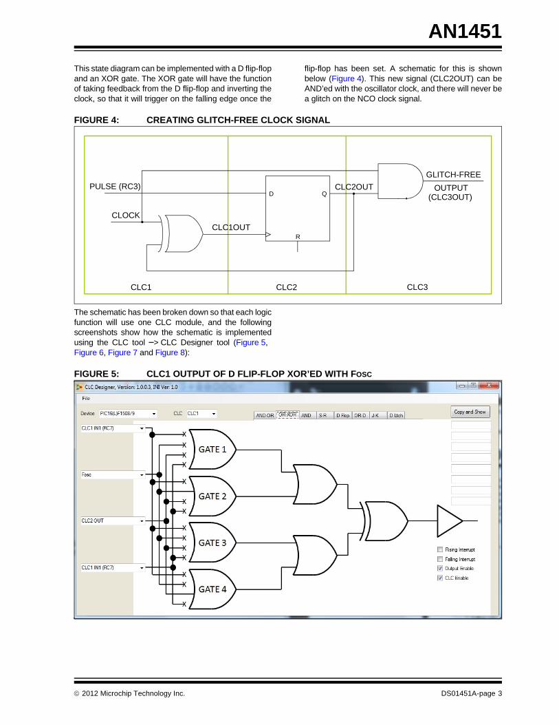
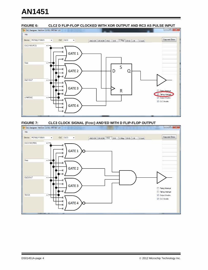
The schematic has been broken down so that each logicfunction will use one CLC module, and the followingscreenshots show how the schematic is implementedusing the CLC tool –> CLC Designer tool (Figure 5, Figure 6, Figure 7 and Figure 8):
FIGURE 5: CLC1 OUTPUT OF D FLIP-FLOP XOR’ED WITH FOSC
D Q
R
PULSE (RC3)
CLOCK
CLC1OUT
CLC2OUT
GLITCH-FREE
OUTPUT(CLC3OUT)
CLC1 CLC2 CLC3
2012 Microchip Technology Inc. DS01451A-page 3
AN1451
FIGURE 6: CLC2 D FLIP-FLOP CLOCKED WITH XOR OUTPUT AND RC3 AS PULSE INPUT
FIGURE 7: CLC3 CLOCK SIGNAL (FOSC) AND’ED WITH D FLIP-FLOP OUTPUT
DS01451A-page 4 2012 Microchip Technology Inc.

AN1451
FIGURE 8: FOSC ROUTED TO RC4 PIN
Once this logic has been implemented, we now have aglitch-free output to drive our NCO clock signal. Thescope plot below (Figure 9) shows the Asynchronousinput signal, FOSC system clock, XOR output
(CLC1OUT), latch output (CLC2OUT), and glitch-freeoutput clock (CLC3OUT). The interrupt flag will be seton the falling edge of the CLC2OUT signal (when weare done measuring our pulse width).
FIGURE 9: GLITCH-FREE CLOCK OUTPUT TO NCO
2012 Microchip Technology Inc. DS01451A-page 5

AN1451
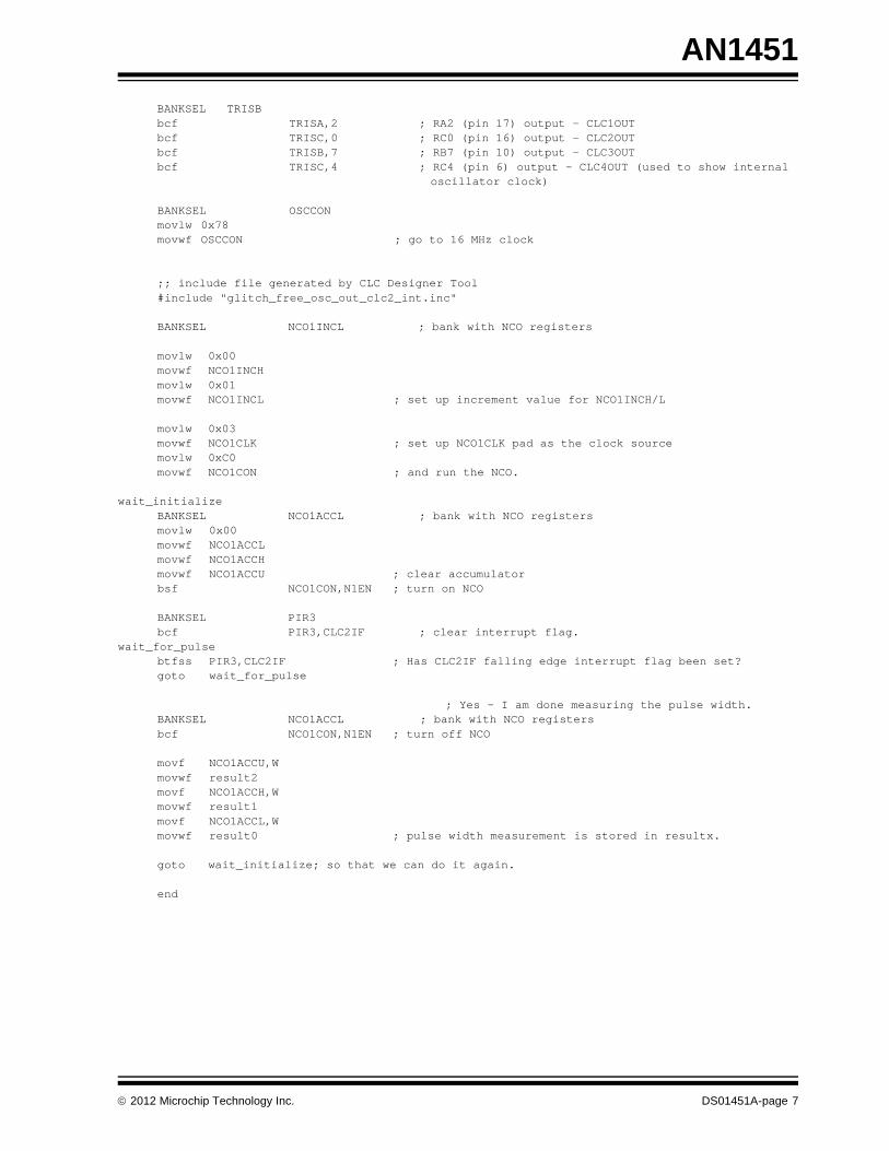
APPENDIX A: ASSEMBLY SOURCE CODE
FileName: glitch_free.asmDependencies: Processor: PIC16F1509Hardware:Compiler: MPASM 5.45 or laterCompany: Microchip Technology, Inc.
Copyright © 2007-2012 Microchip Technology Inc. All rights reserved.
You may use this software, and any derivatives, exclusively with Microchip’s products. Microchip and its licensors retain all ownershipand intellectual property rights in the accompanying software and in all derivatives hereto. This software and any accompanying infor-mation is for suggestion only. It does not modify Microchip’s standard warranty for its products. You agree that you are solely respon-sible for testing the software and determining its suitability. Microchip has no obligation to modify, test, certify, or support the software.
THIS SOFTWARE IS SUPPLIED BY MICROCHIP "AS IS". NO WARRANTIES, WHETHER EXPRESS, IMPLIED OR STATUTORY,INCLUDING, BUT NOT LIMITED TO, IMPLIED WARRANTIES OF NON-INFRINGEMENT, MERCHANTABILITY, AND FITNESS FORA PARTICULAR PURPOSE APPLY TO THIS SOFTWARE, ITS INTERACTION WITH MICROCHIP’S PRODUCTS, COMBINATIONWITH ANY OTHER PRODUCTS, OR USE IN ANY APPLICATION.
IN NO EVENT, WILL MICROCHIP BE LIABLE, WHETHER IN CONTRACT, WARRANTY, TORT (INCLUDING NEGLIGENCE ORBREACH OF STATUTORY DUTY), STRICT LIABILITY, INDEMNITY, CONTRIBUTION, OR OTHERWISE, FOR ANY INDIRECT,SPECIAL, PUNITIVE, EXEMPLARY, INCIDENTAL OR CONSEQUENTIAL LOSS, DAMAGE, FOR COST OR EXPENSE OF ANYKIND WHATSOEVER RELATED TO THE SOFTWARE, HOWSOEVER CAUSED, EVEN IF MICROCHIP HAS BEEN ADVISED OFTHE POSSIBILITY OR THE DAMAGES ARE FORESEEABLE. TO THE FULLEST EXTENT ALLOWABLE BY LAW, MICROCHIP'STOTAL LIABILITY ON ALL CLAIMS IN ANY WAY RELATED TO THIS SOFTWARE WILL NOT EXCEED THE AMOUNT OF FEES, IFANY, THAT YOU HAVE PAID DIRECTLY TO MICROCHIP FOR THIS SOFTWARE.
MICROCHIP PROVIDES THIS SOFTWARE CONDITIONALLY UPON YOUR ACCEPTANCE OF THESE TERMS.
/
#include "p16f1509.inc"
__CONFIG _CONFIG1, _FOSC_INTOSC & _WDTE_OFF & _PWRTE_OFF & _CLKOUTEN_OFF__CONFIG _CONFIG2, _LVP_OFF & _STVREN_ON
errorlevel -302 ;suppress bank selection not zero warning
result0 equ 0x20result1 equ 0x21result2 equ 0x22
ORG 0x00
mainBANKSEL ANSELAclrf ANSELA ; all digital pinsclrf ANSELCclrf ANSELB
Software License AgreementThe software supplied herewith by Microchip Technology Incorporated (the “Company”) is intended and supplied to you, theCompany’s customer, for use solely and exclusively with products manufactured by the Company.The software is owned by the Company and/or its supplier, and is protected under applicable copyright laws. All rights are reserved.Any use in violation of the foregoing restrictions may subject the user to criminal sanctions under applicable laws, as well as to civilliability for the breach of the terms and conditions of this license.THIS SOFTWARE IS PROVIDED IN AN “AS IS” CONDITION. NO WARRANTIES, WHETHER EXPRESS, IMPLIED OR STATU-TORY, INCLUDING, BUT NOT LIMITED TO, IMPLIED WARRANTIES OF MERCHANTABILITY AND FITNESS FOR A PARTICU-LAR PURPOSE APPLY TO THIS SOFTWARE. THE COMPANY SHALL NOT, IN ANY CIRCUMSTANCES, BE LIABLE FORSPECIAL, INCIDENTAL OR CONSEQUENTIAL DAMAGES, FOR ANY REASON WHATSOEVER.
DS01451A-page 6 2012 Microchip Technology Inc.
AN1451
BANKSEL TRISBbcf TRISA,2 ; RA2 (pin 17) output - CLC1OUTbcf TRISC,0 ; RC0 (pin 16) output - CLC2OUTbcf TRISB,7 ; RB7 (pin 10) output - CLC3OUTbcf TRISC,4 ; RC4 (pin 6) output - CLC4OUT (used to show internal
oscillator clock)
BANKSEL OSCCONmovlw 0x78movwf OSCCON ; go to 16 MHz clock
;; include file generated by CLC Designer Tool#include "glitch_free_osc_out_clc2_int.inc"
BANKSEL NCO1INCL ; bank with NCO registers
movlw 0x00movwf NCO1INCHmovlw 0x01movwf NCO1INCL ; set up increment value for NCO1INCH/L
movlw 0x03movwf NCO1CLK ; set up NCO1CLK pad as the clock sourcemovlw 0xC0movwf NCO1CON ; and run the NCO.
wait_initializeBANKSEL NCO1ACCL ; bank with NCO registersmovlw 0x00movwf NCO1ACCLmovwf NCO1ACCHmovwf NCO1ACCU ; clear accumulatorbsf NCO1CON,N1EN ; turn on NCO
BANKSEL PIR3bcf PIR3,CLC2IF ; clear interrupt flag.
wait_for_pulsebtfss PIR3,CLC2IF ; Has CLC2IF falling edge interrupt flag been set?goto wait_for_pulse
; Yes - I am done measuring the pulse width.BANKSEL NCO1ACCL ; bank with NCO registersbcf NCO1CON,N1EN ; turn off NCO
movf NCO1ACCU,Wmovwf result2movf NCO1ACCH,Wmovwf result1movf NCO1ACCL,Wmovwf result0 ; pulse width measurement is stored in resultx.
goto wait_initialize; so that we can do it again.
end
2012 Microchip Technology Inc. DS01451A-page 7
AN1451
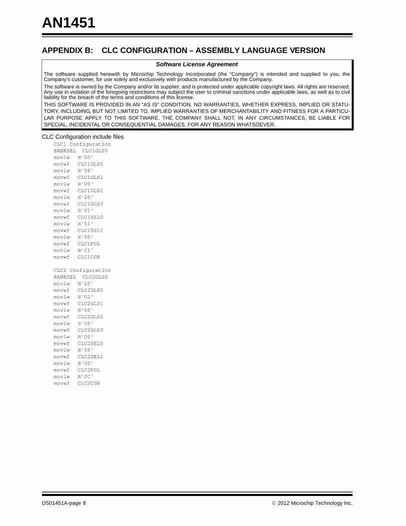
APPENDIX B: CLC CONFIGURATION – ASSEMBLY LANGUAGE VERSION
CLC Configuration include filesCLC1 ConfigurationBANKSEL CLC1GLS0movlw H'00'movwf CLC1GLS0movlw H'08'movwf CLC1GLS1movlw H'00'movwf CLC1GLS2movlw H'20'movwf CLC1GLS3movlw H'01'movwf CLC1SEL0movlw H'51'movwf CLC1SEL1movlw H'00'movwf CLC1POLmovlw H'C1'movwf CLC1CON
CLC2 ConfigurationBANKSEL CLC2GLS0movlw H'20'movwf CLC2GLS0movlw H'02'movwf CLC2GLS1movlw H'00'movwf CLC2GLS2movlw H'00'movwf CLC2GLS3movlw H'00'movwf CLC2SEL0movlw H'00'movwf CLC2SEL1movlw H'00'movwf CLC2POLmovlw H'CC'movwf CLC2CON
Software License AgreementThe software supplied herewith by Microchip Technology Incorporated (the “Company”) is intended and supplied to you, theCompany’s customer, for use solely and exclusively with products manufactured by the Company.The software is owned by the Company and/or its supplier, and is protected under applicable copyright laws. All rights are reserved.Any use in violation of the foregoing restrictions may subject the user to criminal sanctions under applicable laws, as well as to civilliability for the breach of the terms and conditions of this license.THIS SOFTWARE IS PROVIDED IN AN “AS IS” CONDITION. NO WARRANTIES, WHETHER EXPRESS, IMPLIED OR STATU-TORY, INCLUDING, BUT NOT LIMITED TO, IMPLIED WARRANTIES OF MERCHANTABILITY AND FITNESS FOR A PARTICU-LAR PURPOSE APPLY TO THIS SOFTWARE. THE COMPANY SHALL NOT, IN ANY CIRCUMSTANCES, BE LIABLE FORSPECIAL, INCIDENTAL OR CONSEQUENTIAL DAMAGES, FOR ANY REASON WHATSOEVER.
DS01451A-page 8 2012 Microchip Technology Inc.
AN1451
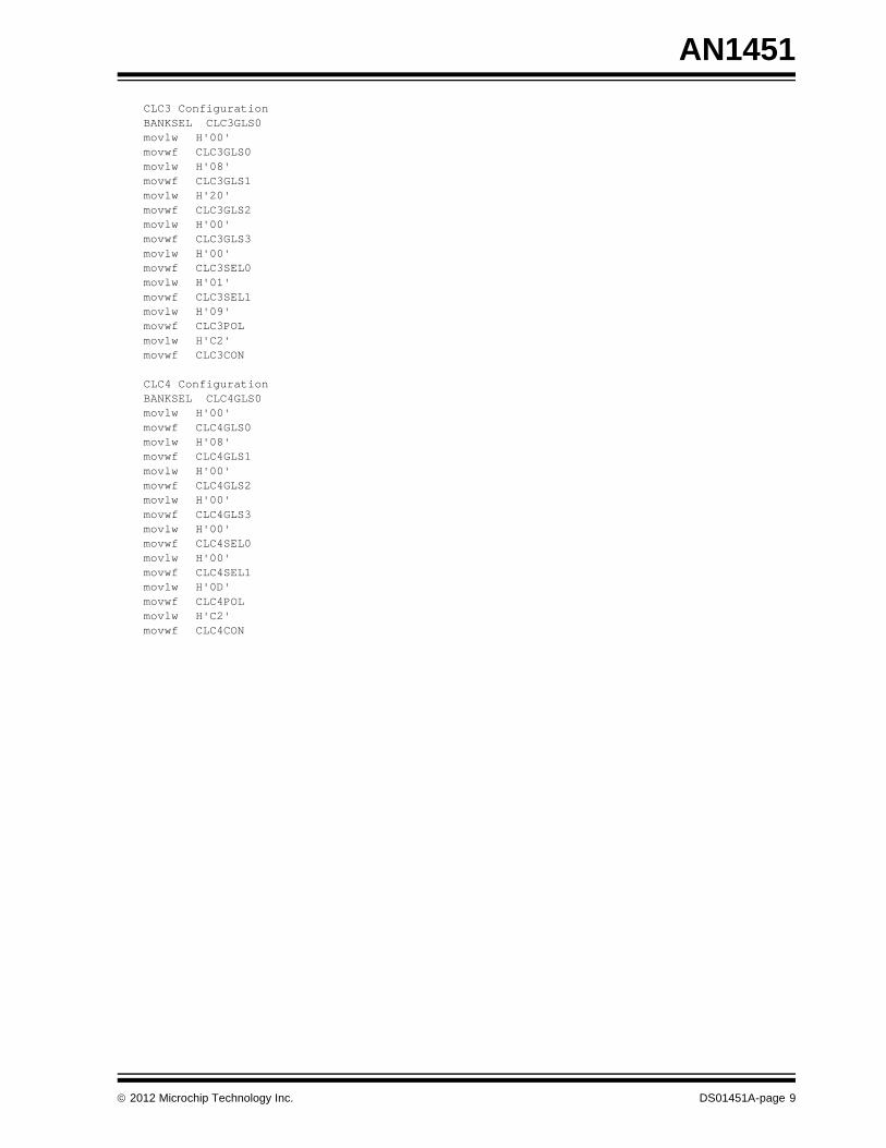
CLC3 ConfigurationBANKSEL CLC3GLS0movlw H'00'movwf CLC3GLS0movlw H'08'movwf CLC3GLS1movlw H'20'movwf CLC3GLS2movlw H'00'movwf CLC3GLS3movlw H'00'movwf CLC3SEL0movlw H'01'movwf CLC3SEL1movlw H'09'movwf CLC3POLmovlw H'C2'movwf CLC3CON
CLC4 ConfigurationBANKSEL CLC4GLS0movlw H'00'movwf CLC4GLS0movlw H'08'movwf CLC4GLS1movlw H'00'movwf CLC4GLS2movlw H'00'movwf CLC4GLS3movlw H'00'movwf CLC4SEL0movlw H'00'movwf CLC4SEL1movlw H'0D'movwf CLC4POLmovlw H'C2'movwf CLC4CON
2012 Microchip Technology Inc. DS01451A-page 9
AN1451
NOTES:
DS01451A-page 10 2012 Microchip Technology Inc.
Note the following details of the code protection feature on Microchip devices:
• Microchip products meet the specification contained in their particular Microchip Data Sheet.
• Microchip believes that its family of products is one of the most secure families of its kind on the market today, when used in the intended manner and under normal conditions.
• There are dishonest and possibly illegal methods used to breach the code protection feature. All of these methods, to our knowledge, require using the Microchip products in a manner outside the operating specifications contained in Microchip’s Data Sheets. Most likely, the person doing so is engaged in theft of intellectual property.
• Microchip is willing to work with the customer who is concerned about the integrity of their code.
• Neither Microchip nor any other semiconductor manufacturer can guarantee the security of their code. Code protection does not mean that we are guaranteeing the product as “unbreakable.”
Code protection is constantly evolving. We at Microchip are committed to continuously improving the code protection features of ourproducts. Attempts to break Microchip’s code protection feature may be a violation of the Digital Millennium Copyright Act. If such actsallow unauthorized access to your software or other copyrighted work, you may have a right to sue for relief under that Act.
Information contained in this publication regarding deviceapplications and the like is provided only for your convenienceand may be superseded by updates. It is your responsibility toensure that your application meets with your specifications.MICROCHIP MAKES NO REPRESENTATIONS ORWARRANTIES OF ANY KIND WHETHER EXPRESS ORIMPLIED, WRITTEN OR ORAL, STATUTORY OROTHERWISE, RELATED TO THE INFORMATION,INCLUDING BUT NOT LIMITED TO ITS CONDITION,QUALITY, PERFORMANCE, MERCHANTABILITY ORFITNESS FOR PURPOSE. Microchip disclaims all liabilityarising from this information and its use. Use of Microchipdevices in life support and/or safety applications is entirely atthe buyer’s risk, and the buyer agrees to defend, indemnify andhold harmless Microchip from any and all damages, claims,suits, or expenses resulting from such use. No licenses areconveyed, implicitly or otherwise, under any Microchipintellectual property rights.
2012 Microchip Technology Inc.
QUALITY MANAGEMENT SYSTEM CERTIFIED BY DNV
== ISO/TS 16949 ==
Trademarks
The Microchip name and logo, the Microchip logo, dsPIC, KEELOQ, KEELOQ logo, MPLAB, PIC, PICmicro, PICSTART, PIC32 logo, rfPIC and UNI/O are registered trademarks of Microchip Technology Incorporated in the U.S.A. and other countries.
FilterLab, Hampshire, HI-TECH C, Linear Active Thermistor, MXDEV, MXLAB, SEEVAL and The Embedded Control Solutions Company are registered trademarks of Microchip Technology Incorporated in the U.S.A.
Analog-for-the-Digital Age, Application Maestro, chipKIT, chipKIT logo, CodeGuard, dsPICDEM, dsPICDEM.net, dsPICworks, dsSPEAK, ECAN, ECONOMONITOR, FanSense, HI-TIDE, In-Circuit Serial Programming, ICSP, Mindi, MiWi, MPASM, MPLAB Certified logo, MPLIB, MPLINK, mTouch, Omniscient Code Generation, PICC, PICC-18, PICDEM, PICDEM.net, PICkit, PICtail, REAL ICE, rfLAB, Select Mode, Total Endurance, TSHARC, UniWinDriver, WiperLock and ZENA are trademarks of Microchip Technology Incorporated in the U.S.A. and other countries.
SQTP is a service mark of Microchip Technology Incorporated in the U.S.A.
All other trademarks mentioned herein are property of their respective companies.
© 2012, Microchip Technology Incorporated, Printed in the U.S.A., All Rights Reserved.
Printed on recycled paper.
ISBN: 9781620764503
DS01451A-page 11
Microchip received ISO/TS-16949:2009 certification for its worldwide headquarters, design and wafer fabrication facilities in Chandler and Tempe, Arizona; Gresham, Oregon and design centers in California and India. The Company’s quality system processes and procedures are for its PIC® MCUs and dsPIC® DSCs, KEELOQ® code hopping devices, Serial EEPROMs, microperipherals, nonvolatile memory and analog products. In addition, Microchip’s quality system for the design and manufacture of development systems is ISO 9001:2000 certified.
DS01451A-page 12 2012 Microchip Technology Inc.
AMERICASCorporate Office2355 West Chandler Blvd.Chandler, AZ 85224-6199Tel: 480-792-7200 Fax: 480-792-7277Technical Support: http://www.microchip.com/supportWeb Address: www.microchip.com
AtlantaDuluth, GA Tel: 678-957-9614 Fax: 678-957-1455
BostonWestborough, MA Tel: 774-760-0087 Fax: 774-760-0088
ChicagoItasca, IL Tel: 630-285-0071 Fax: 630-285-0075
ClevelandIndependence, OH Tel: 216-447-0464 Fax: 216-447-0643
DallasAddison, TX Tel: 972-818-7423 Fax: 972-818-2924
DetroitFarmington Hills, MI Tel: 248-538-2250Fax: 248-538-2260
IndianapolisNoblesville, IN Tel: 317-773-8323Fax: 317-773-5453
Los AngelesMission Viejo, CA Tel: 949-462-9523 Fax: 949-462-9608
Santa ClaraSanta Clara, CA Tel: 408-961-6444Fax: 408-961-6445
TorontoMississauga, Ontario, CanadaTel: 905-673-0699 Fax: 905-673-6509
ASIA/PACIFICAsia Pacific OfficeSuites 3707-14, 37th FloorTower 6, The GatewayHarbour City, KowloonHong KongTel: 852-2401-1200Fax: 852-2401-3431
Australia - SydneyTel: 61-2-9868-6733Fax: 61-2-9868-6755
China - BeijingTel: 86-10-8569-7000 Fax: 86-10-8528-2104
China - ChengduTel: 86-28-8665-5511Fax: 86-28-8665-7889
China - ChongqingTel: 86-23-8980-9588Fax: 86-23-8980-9500
China - HangzhouTel: 86-571-2819-3187 Fax: 86-571-2819-3189
China - Hong Kong SARTel: 852-2401-1200 Fax: 852-2401-3431
China - NanjingTel: 86-25-8473-2460Fax: 86-25-8473-2470
China - QingdaoTel: 86-532-8502-7355Fax: 86-532-8502-7205
China - ShanghaiTel: 86-21-5407-5533 Fax: 86-21-5407-5066
China - ShenyangTel: 86-24-2334-2829Fax: 86-24-2334-2393
China - ShenzhenTel: 86-755-8203-2660 Fax: 86-755-8203-1760
China - WuhanTel: 86-27-5980-5300Fax: 86-27-5980-5118
China - XianTel: 86-29-8833-7252Fax: 86-29-8833-7256
China - XiamenTel: 86-592-2388138 Fax: 86-592-2388130
China - ZhuhaiTel: 86-756-3210040 Fax: 86-756-3210049
ASIA/PACIFICIndia - BangaloreTel: 91-80-3090-4444 Fax: 91-80-3090-4123
India - New DelhiTel: 91-11-4160-8631Fax: 91-11-4160-8632
India - PuneTel: 91-20-2566-1512Fax: 91-20-2566-1513
Japan - OsakaTel: 81-66-152-7160 Fax: 81-66-152-9310
Japan - YokohamaTel: 81-45-471- 6166 Fax: 81-45-471-6122
Korea - DaeguTel: 82-53-744-4301Fax: 82-53-744-4302
Korea - SeoulTel: 82-2-554-7200Fax: 82-2-558-5932 or 82-2-558-5934
Malaysia - Kuala LumpurTel: 60-3-6201-9857Fax: 60-3-6201-9859
Malaysia - PenangTel: 60-4-227-8870Fax: 60-4-227-4068
Philippines - ManilaTel: 63-2-634-9065Fax: 63-2-634-9069
SingaporeTel: 65-6334-8870Fax: 65-6334-8850
Taiwan - Hsin ChuTel: 886-3-5778-366Fax: 886-3-5770-955
Taiwan - KaohsiungTel: 886-7-536-4818Fax: 886-7-330-9305
Taiwan - TaipeiTel: 886-2-2500-6610 Fax: 886-2-2508-0102
Thailand - BangkokTel: 66-2-694-1351Fax: 66-2-694-1350
EUROPEAustria - WelsTel: 43-7242-2244-39Fax: 43-7242-2244-393Denmark - CopenhagenTel: 45-4450-2828 Fax: 45-4485-2829
France - ParisTel: 33-1-69-53-63-20 Fax: 33-1-69-30-90-79
Germany - MunichTel: 49-89-627-144-0 Fax: 49-89-627-144-44
Italy - Milan Tel: 39-0331-742611 Fax: 39-0331-466781
Netherlands - DrunenTel: 31-416-690399 Fax: 31-416-690340
Spain - MadridTel: 34-91-708-08-90Fax: 34-91-708-08-91
UK - WokinghamTel: 44-118-921-5869Fax: 44-118-921-5820
Worldwide Sales and Service
11/29/11


![THOUGHTS ON GLITCH[ART]v2 - Nick Briznickbriz.com/thoughtsonglitchart/thoughtsonglitchartv2.0.pdfTHOUGHTS ON GLITCH[ART]v2.0 0 whois ( preface ) 1 how to glitch art 2 ..... definitions](https://img.pdfslide.us/doc/110x75/5ae5ff047f8b9a08778c6f37/thoughts-on-glitchartv2-nick-on-glitchartv20-0-whois-preface-1-how-to.jpg)