Embed Size (px)
Citation preview
Sandia National Laboratories is a multimissionlaboratory managed and operated by National Technology & Engineering Solutions of Sandia, LLC, a wholly owned subsidiary of Honeywell International Inc., for the U.S. Department of
Energy’s National Nuclear Security Administration under contract DE-NA0003525.
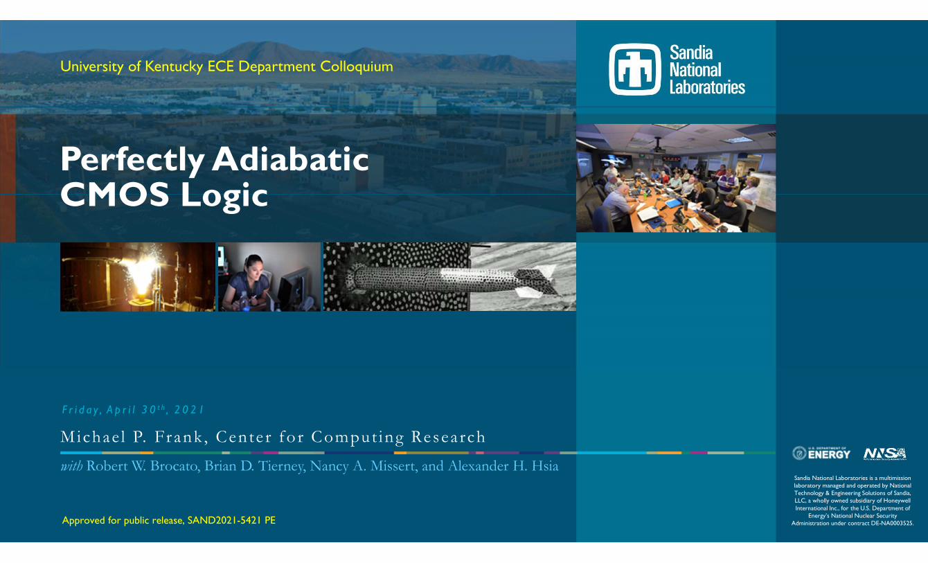
Perfectly Adiabatic CMOS Logic
Michae l P. Frank , Cente r fo r Comput ing Resea rch
F r i d a y , A p r i l 3 0 t h , 2 0 2 1
University of Kentucky ECE Department Colloquium
Approved for public release, SAND2021-5421 PE
with Robert W. Brocato, Brian D. Tierney, Nancy A. Missert, and Alexander H. Hsia
Text of Talk Abstract (hide during talk)
The concept of adiabatic logic in CMOS has a long history, but until recently, very few of the adiabatic logic families in the literature were truly, fully adiabatic—that is, all the way down to the limit set by leakage—and even the known fully adiabatic logic families were not fully static, resulting in practical limitations due to perturbations of floating node voltages through parasitic capacitive couplings. Last year, the first CMOS logic family that is both fully static and truly, fully adiabatic—S2LAL—was invented and published. We call such logic families perfectly adiabatic, since their minimum dissipation is only limited by leakage even when accounting for realistic parasitics. S2LAL is a quad-rail logic, but since then, simplified variations have been developed. We conjecture, however, that any perfectly adiabatic sequential CMOS logic family requires at least 8 transition times or “ticks” per clock cycle, as is the case in S2LAL. We believe that perfectly adiabatic CMOS logic families in low-leakage processes have the potential to set new records for the energy efficiency of semiconductor-based logic, and can also have significant applications in computer security.
2
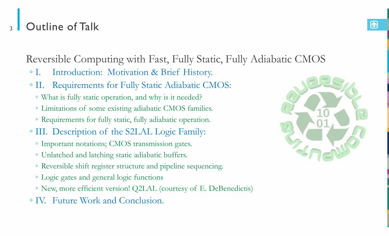
Outline of Talk
Reversible Computing with Fast, Fully Static, Fully Adiabatic CMOS I. Introduction: Motivation & Brief History. II. Requirements for Fully Static Adiabatic CMOS:
What is fully static operation, and why is it needed? Limitations of some existing adiabatic CMOS families. Requirements for fully static, fully adiabatic operation.
III. Description of the S2LAL Logic Family: Important notations; CMOS transmission gates. Unlatched and latching static adiabatic buffers. Reversible shift register structure and pipeline sequencing. Logic gates and general logic functions New, more efficient version! Q2LAL (courtesy of E. DeBenedictis)
IV. Future Work and Conclusion.
3

Section I. Motivation & History
Per fec t l y Ad iaba t i c CMOS Log ic
Motivation & Brief History
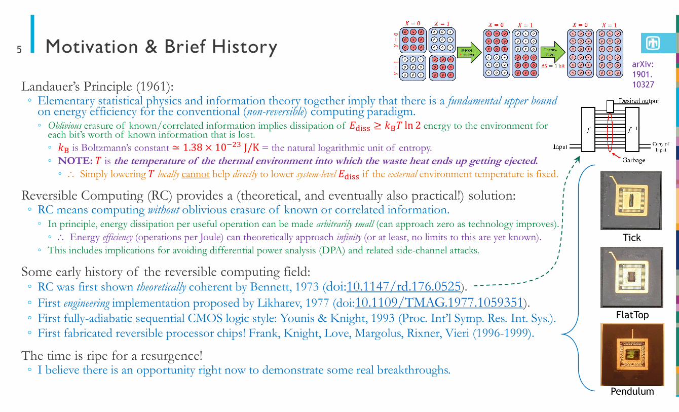
Landauer’s Principle (1961): Elementary statistical physics and information theory together imply that there is a fundamental upper bound
on energy efficiency for the conventional (non-reversible) computing paradigm. Oblivious erasure of known/correlated information implies dissipation of 𝐸 ≥ 𝑘 𝑇 ln 2 energy to the environment for
each bit’s worth of known information that is lost. 𝑘 is Boltzmann’s constant ≃ 1.38 × 10 J/K = the natural logarithmic unit of entropy. NOTE: 𝑇 is the temperature of the thermal environment into which the waste heat ends up getting ejected.
Simply lowering 𝑇 locally cannot help directly to lower system-level 𝐸 if the external environment temperature is fixed.
Reversible Computing (RC) provides a (theoretical, and eventually also practical!) solution: RC means computing without oblivious erasure of known or correlated information.
In principle, energy dissipation per useful operation can be made arbitrarily small (can approach zero as technology improves). Energy efficiency (operations per Joule) can theoretically approach infinity (or at least, no limits to this are yet known).
This includes implications for avoiding differential power analysis (DPA) and related side-channel attacks.
Some early history of the reversible computing field: RC was first shown theoretically coherent by Bennett, 1973 (doi:10.1147/rd.176.0525). First engineering implementation proposed by Likharev, 1977 (doi:10.1109/TMAG.1977.1059351). First fully-adiabatic sequential CMOS logic style: Younis & Knight, 1993 (Proc. Int’l Symp. Res. Int. Sys.). First fabricated reversible processor chips! Frank, Knight, Love, Margolus, Rixner, Vieri (1996-1999).
The time is ripe for a resurgence! I believe there is an opportunity right now to demonstrate some real breakthroughs.
5arXiv:1901.10327
Pendulum
FlatTop
Tick
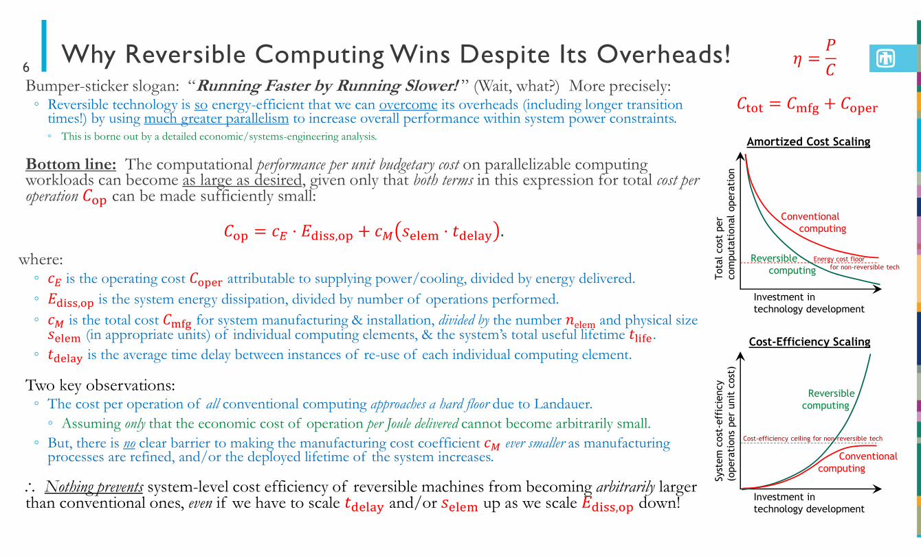
Why Reversible Computing Wins Despite Its Overheads!Bumper-sticker slogan: “Running Faster by Running Slower! ” (Wait, what?) More precisely: Reversible technology is so energy-efficient that we can overcome its overheads (including longer transition
times!) by using much greater parallelism to increase overall performance within system power constraints. This is borne out by a detailed economic/systems-engineering analysis.
Bottom line: The computational performance per unit budgetary cost on parallelizable computing workloads can become as large as desired, given only that both terms in this expression for total cost per operation can be made sufficiently small:
,
where: 𝑐 is the operating cost 𝐶 attributable to supplying power/cooling, divided by energy delivered. 𝐸 , is the system energy dissipation, divided by number of operations performed. 𝑐 is the total cost 𝐶 for system manufacturing & installation, divided by the number 𝑛elem and physical size
𝑠 (in appropriate units) of individual computing elements, & the system’s total useful lifetime 𝑡 . 𝑡 is the average time delay between instances of re-use of each individual computing element.
Two key observations: The cost per operation of all conventional computing approaches a hard floor due to Landauer.
Assuming only that the economic cost of operation per Joule delivered cannot become arbitrarily small. But, there is no clear barrier to making the manufacturing cost coefficient 𝑐 ever smaller as manufacturing
processes are refined, and/or the deployed lifetime of the system increases.
Nothing prevents system-level cost efficiency of reversible machines from becoming arbitrarily larger than conventional ones, even if we have to scale and/or up as we scale , down!
6
Investment intechnology development
Tota
l co
st p
erco
mpu
tati
onal
ope
rati
on
Energy cost floor for non-reversible tech
Conventional computing
Reversiblecomputing
Amortized Cost Scaling
Investment intechnology development
Syst
em c
ost-
effi
cien
cy
(ope
rati
ons
per
unit
cos
t)
Conventionalcomputing
Reversiblecomputing
Cost-efficiency ceiling for non-reversible tech
Cost-Efficiency Scaling
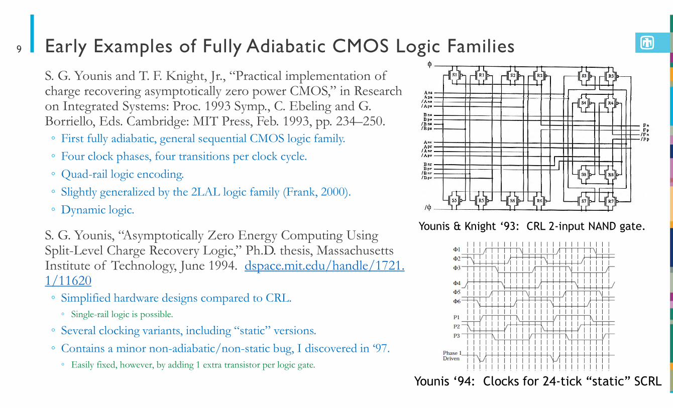
Early Examples of Fully Adiabatic CMOS Logic Families9
Younis ‘94: Clocks for 24-tick “static” SCRL
Younis & Knight ‘93: CRL 2-input NAND gate.
S. G. Younis and T. F. Knight, Jr., “Practical implementation of charge recovering asymptotically zero power CMOS,” in Research on Integrated Systems: Proc. 1993 Symp., C. Ebeling and G. Borriello, Eds. Cambridge: MIT Press, Feb. 1993, pp. 234–250. First fully adiabatic, general sequential CMOS logic family.
Four clock phases, four transitions per clock cycle.
Quad-rail logic encoding. Slightly generalized by the 2LAL logic family (Frank, 2000).
Dynamic logic.
S. G. Younis, “Asymptotically Zero Energy Computing Using Split-Level Charge Recovery Logic,” Ph.D. thesis, Massachusetts Institute of Technology, June 1994. dspace.mit.edu/handle/1721. 1/11620 Simplified hardware designs compared to CRL.
Single-rail logic is possible.
Several clocking variants, including “static” versions.
Contains a minor non-adiabatic/non-static bug, I discovered in ‘97. Easily fixed, however, by adding 1 extra transistor per logic gate.
Goal of This Work
Design a new sequential, pipelined adiabatic CMOS logic family with the following features:1. Fully adiabatic operation.
I.e., no non-adiabatic “spark” or “squelch” events occur in an ideal setting. I.e., given negligible leakage and parasitic couplings.
2. Fully static operation. I.e., each circuit node is connected to a supply at all times.
Note, this feature facilitates elimination of non-adiabatic events even in non-ideal settings.
3. Minimal latency. I.e., only one “tick” or transition time of delay per layer of combinational logic depth.
4. Maximum throughput. I.e., the number of ticks per initiation interval should also be minimal.
Conjecture: Minimum clock period meeting other design goals is 8 ticks (achieved in this work).
10
Section II. Requirements
Per fec t l y Ad iaba t i c CMOS Log ic
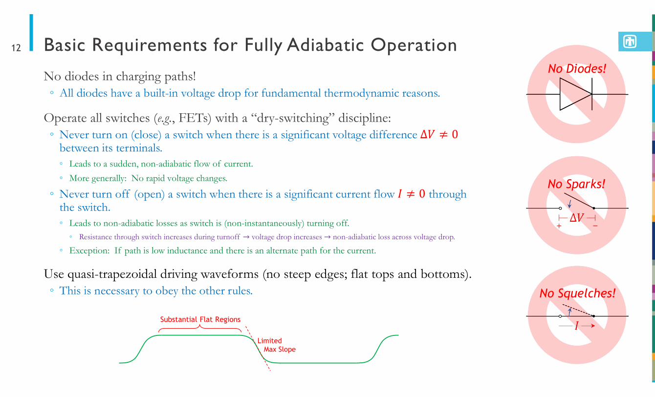
Basic Requirements for Fully Adiabatic Operation
No diodes in charging paths! All diodes have a built-in voltage drop for fundamental thermodynamic reasons.
Operate all switches (e.g., FETs) with a “dry-switching” discipline: Never turn on (close) a switch when there is a significant voltage difference
between its terminals. Leads to a sudden, non-adiabatic flow of current.
More generally: No rapid voltage changes.
Never turn off (open) a switch when there is a significant current flow through the switch. Leads to non-adiabatic losses as switch is (non-instantaneously) turning off.
Resistance through switch increases during turnoff → voltage drop increases → non-adiabatic loss across voltage drop.
Exception: If path is low inductance and there is an alternate path for the current.
Use quasi-trapezoidal driving waveforms (no steep edges; flat tops and bottoms). This is necessary to obey the other rules.
12
+ −
No Diodes!
No Squelches!
No Sparks!
Substantial Flat Regions
Limited Max Slope
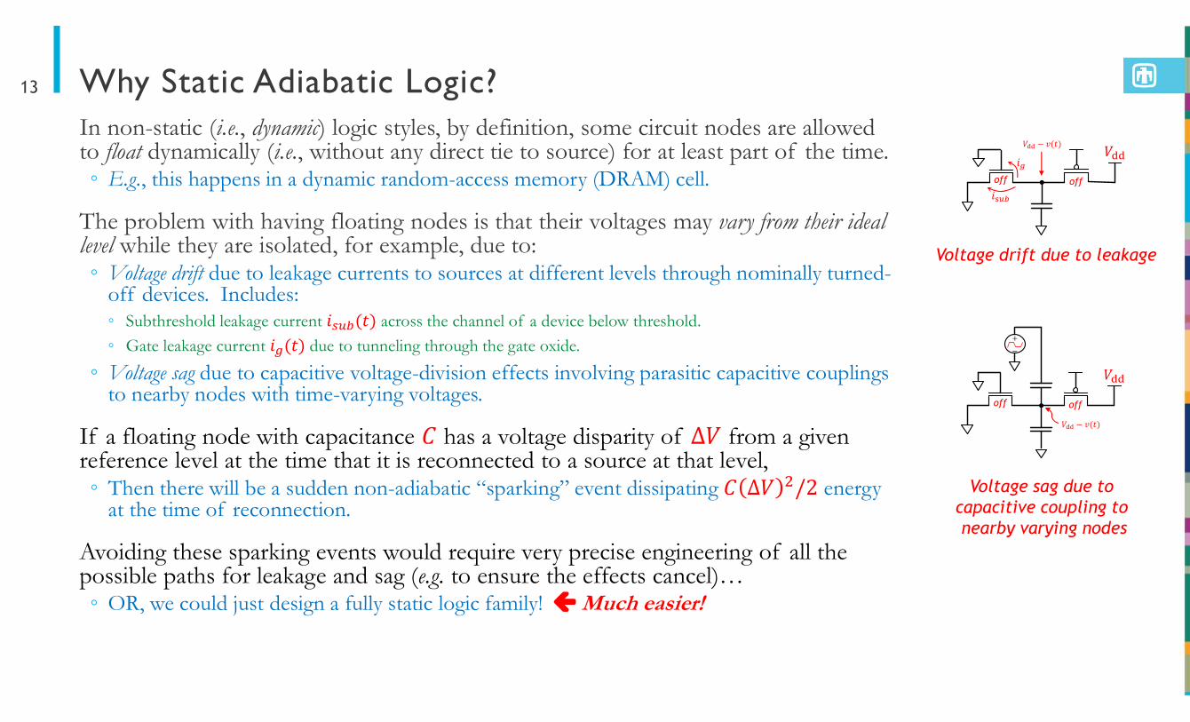
Why Static Adiabatic Logic?In non-static (i.e., dynamic) logic styles, by definition, some circuit nodes are allowed to float dynamically (i.e., without any direct tie to source) for at least part of the time. E.g., this happens in a dynamic random-access memory (DRAM) cell.
The problem with having floating nodes is that their voltages may vary from their ideal level while they are isolated, for example, due to: Voltage drift due to leakage currents to sources at different levels through nominally turned-
off devices. Includes: Subthreshold leakage current 𝑖 (𝑡) across the channel of a device below threshold.
Gate leakage current 𝑖 (𝑡) due to tunneling through the gate oxide.
Voltage sag due to capacitive voltage-division effects involving parasitic capacitive couplings to nearby nodes with time-varying voltages.
If a floating node with capacitance has a voltage disparity of from a given reference level at the time that it is reconnected to a source at that level, Then there will be a sudden non-adiabatic “sparking” event dissipating energy
at the time of reconnection.
Avoiding these sparking events would require very precise engineering of all the possible paths for leakage and sag (e.g. to ensure the effects cancel)… OR, we could just design a fully static logic family! Much easier!
13
𝑉
offoff
𝑖
𝑖
𝑉 − 𝑣(𝑡)
Voltage drift due to leakage
𝑉
offoff
𝑉 − 𝑣(𝑡)
+
−
Voltage sag due to capacitive coupling to nearby varying nodes
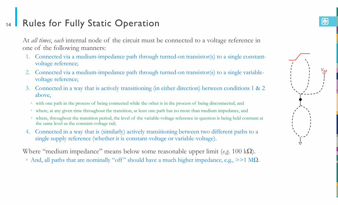
Rules for Fully Static Operation
At all times, each internal node of the circuit must be connected to a voltage reference in one of the following manners:1. Connected via a medium-impedance path through turned-on transistor(s) to a single constant-
voltage reference;
2. Connected via a medium-impedance path through turned-on transistor(s) to a single variable-voltage reference;
3. Connected in a way that is actively transitioning (in either direction) between conditions 1 & 2 above,
with one path in the process of being connected while the other is in the process of being disconnected, and
where, at any given time throughout the transition, at least one path has no more than medium impedance, and
where, throughout the transition period, the level of the variable-voltage reference in question is being held constant at the same level as the constant-voltage rail;
4. Connected in a way that is (similarly) actively transitioning between two different paths to a single supply reference (whether it is constant-voltage or variable-voltage).
Where “medium impedance” means below some reasonable upper limit (e.g. 100 kΩ). And, all paths that are nominally “off ” should have a much higher impedance, e.g., >>1 MΩ.
14
𝑉
Section III. S2LAL Description
Per fec t l y Ad iaba t i c CMOS Log ic
Notations and Conventions Used (slide 1 of 2)Two nominal voltage levels: 0 V (GND, “low”) and (“high”).
Divide time into equal, discrete intervals called ticks, each of duration , and numbered consecutively. Every transition between nominal levels is required to fit entirely within a tick,
so, the actual transition time 𝜏 is upper-bounded by the tick length, 𝜏 ≤ 𝜏 .
The active energy dissipation from any given adiabatic transition is as follows:
where: is a constant shape factor that accounts for the departure of the ramp shape from the ideal; is the capacitive load of the node that is transitioning; is the effective resistance of the charging path.
The clock period is an integer number of ticks, . Thus, the clock frequency is
Ticks within a cycle are numbered modulo n (i.e., ).
16
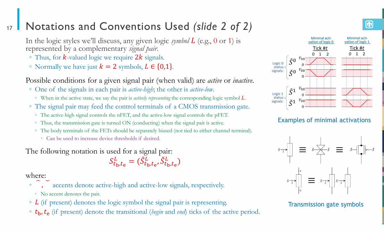
Notations and Conventions Used (slide 2 of 2)In the logic styles we’ll discuss, any given logic symbol (e.g., 0 or 1) is represented by a complementary signal pair. Thus, for -valued logic we require signals. Normally we have just symbols, .
Possible conditions for a given signal pair (when valid) are active or inactive. One of the signals in each pair is active-high; the other is active-low.
When in the active state, we say the pair is actively representing the corresponding logic symbol 𝐿.
The signal pair may feed the control terminals of a CMOS transmission gate. The active-high signal controls the nFET, and the active-low signal controls the pFET. Thus, the transmission gate is turned ON (conducting) when the signal pair is active. The body terminals of the FETs should be separately biased (not tied to either channel terminal).
Can be used to increase device thresholds if desired.
The following notation is used for a signal pair:
, , ,
where: accents denote active-high and active-low signals, respectively.
No accent denotes the pair.
(if present) denotes the logic symbol the signal pair is representing. (if present) denote the transitional (begin and end) ticks of the active period.
17
Examples of minimal activations
Transmission gate symbols
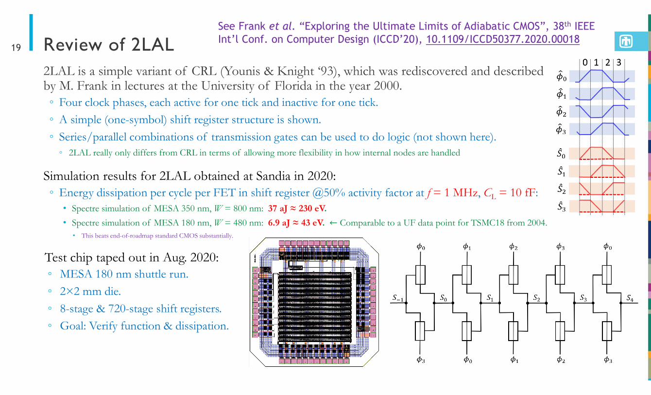
Review of 2LAL2LAL is a simple variant of CRL (Younis & Knight ‘93), which was rediscovered and described by M. Frank in lectures at the University of Florida in the year 2000. Four clock phases, each active for one tick and inactive for one tick. A simple (one-symbol) shift register structure is shown.
Series/parallel combinations of transmission gates can be used to do logic (not shown here). 2LAL really only differs from CRL in terms of allowing more flexibility in how internal nodes are handled
Simulation results for 2LAL obtained at Sandia in 2020: Energy dissipation per cycle per FET in shift register @50% activity factor at f = 1 MHz, CL = 10 fF:
• Spectre simulation of MESA 350 nm, W = 800 nm: 37 aJ ≈ 230 eV.
• Spectre simulation of MESA 180 nm, W = 480 nm: 6.9 aJ ≈ 43 eV. ← Comparable to a UF data point for TSMC18 from 2004.• This beats end-of-roadmap standard CMOS substantially.
Test chip taped out in Aug. 2020: MESA 180 nm shuttle run.
2×2 mm die.
8-stage & 720-stage shift registers. Goal: Verify function & dissipation.
19
See Frank et al. “Exploring the Ultimate Limits of Adiabatic CMOS”, 38th IEEEInt’l Conf. on Computer Design (ICCD’20), 10.1109/ICCD50377.2020.00018
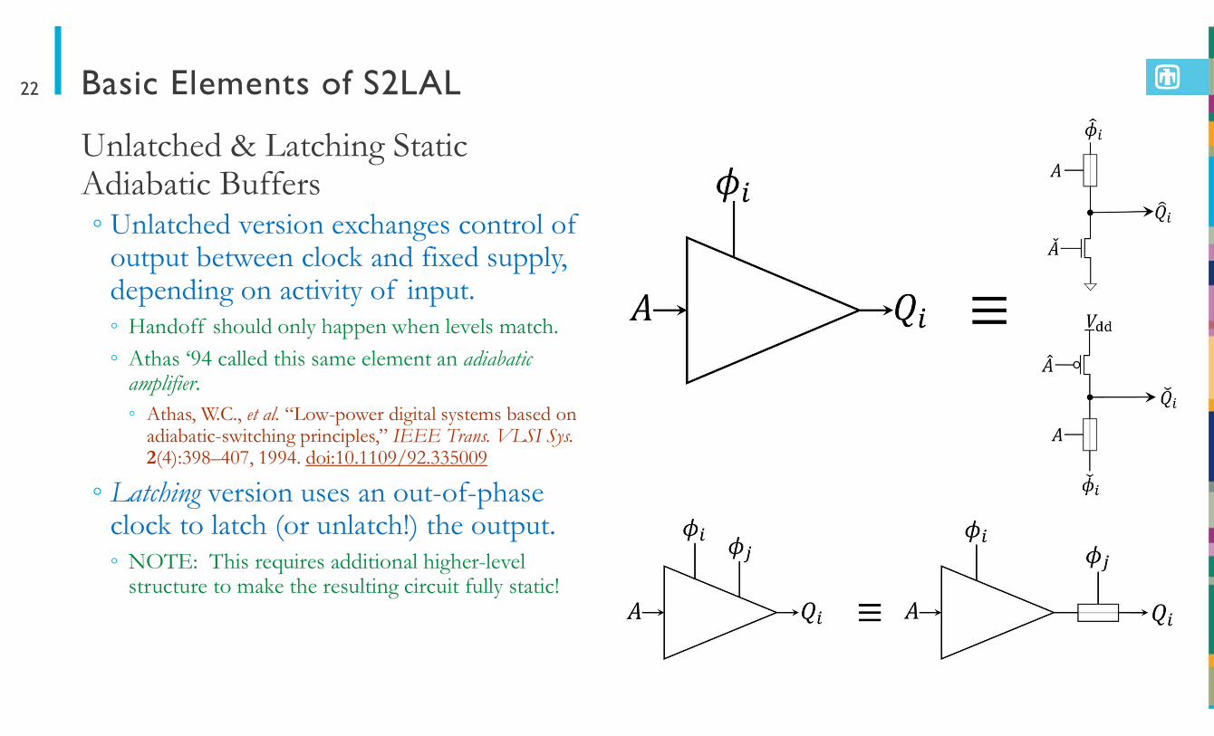
Basic Elements of S2LAL
Unlatched & Latching Static Adiabatic Buffers Unlatched version exchanges control of
output between clock and fixed supply, depending on activity of input. Handoff should only happen when levels match.
Athas ‘94 called this same element an adiabatic amplifier. Athas, W.C., et al. “Low-power digital systems based on
adiabatic-switching principles,” IEEE Trans. VLSI Sys.2(4):398–407, 1994. doi:10.1109/92.335009
Latching version uses an out-of-phase clock to latch (or unlatch!) the output. NOTE: This requires additional higher-level
structure to make the resulting circuit fully static!
22

S2LAL Reversible Pipeline StructurePaired forward and reverse stages: Forward stages activate to compute later signals from earlier ones. Reverse stages de-activate to de-compute earlier signals from later
ones.
Every signal must stay active for (at least) 5 ticks: Provides sufficient time for the following sequence of steps:
(1) Activate forwards stage F , (2) Activate reverse stage R , (3) Handoff control of 𝑆 from F to R , (4) Deactivate forwards stage F , (5) Deactivate reverse stage R .
Add 3 ticks for transitions & inactive handoff: Total cycle length = 8 ticks min.
Note control of each signal is handed off to forward stage 𝑖 on ticks # , and to reverse stage on ticks # . Signal goes valid on ticks # and invalid (inactive) on ticks
# .
For general logic, functions must be invertible. Optimizing whole pipeline gets into reversible algorithm
design: Considered out of scope for this particular paper.
23
Frank et al., “Reversible Computing with Fast, Fully Static, Fully Adiabatic CMOS,” IEEE Int’l Conf. on Rebooting Computing (ICRC ’20), 10.1109/ICRC2020.2020.00014
S2LAL Logic Gates
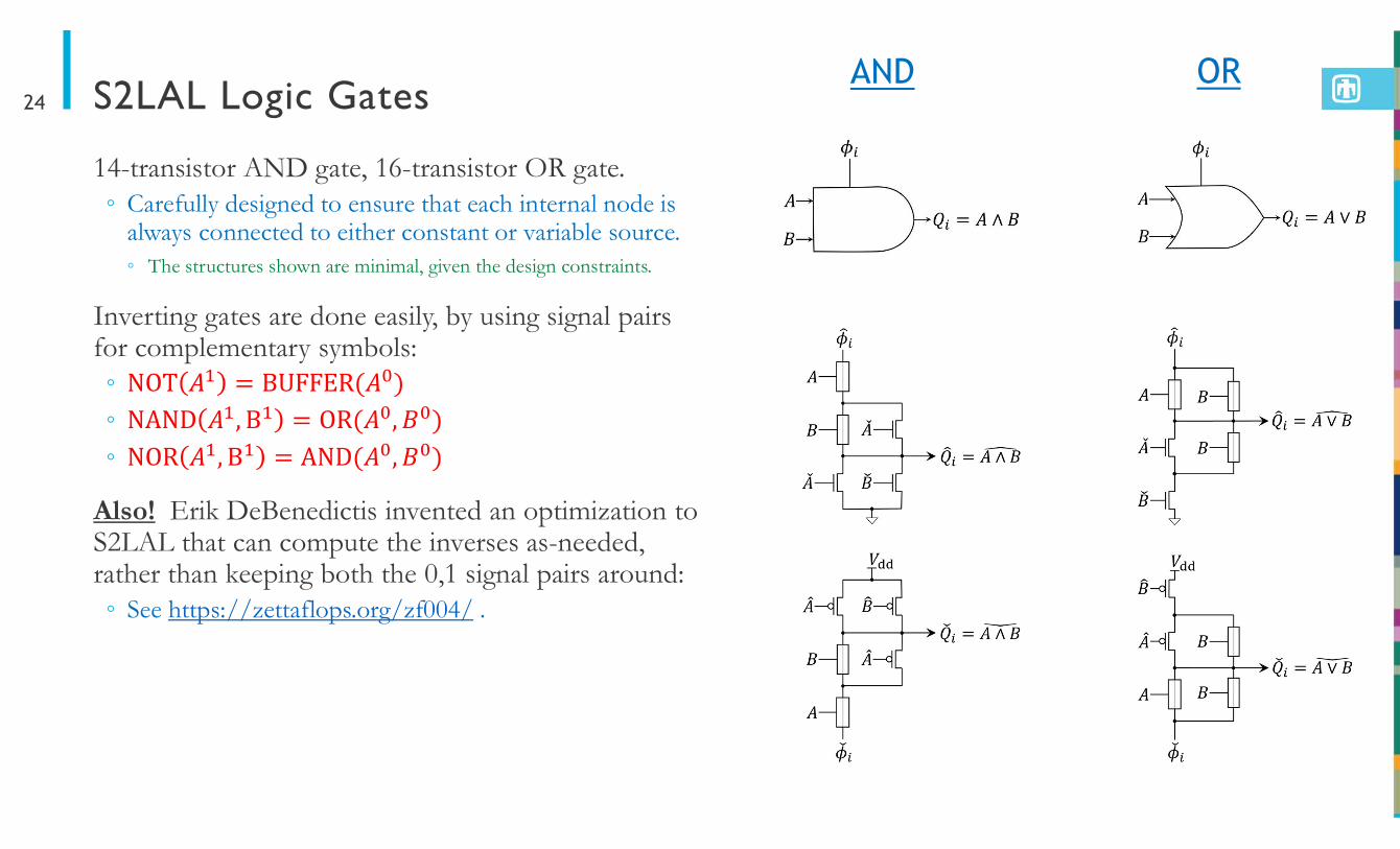
14-transistor AND gate, 16-transistor OR gate. Carefully designed to ensure that each internal node is
always connected to either constant or variable source. The structures shown are minimal, given the design constraints.
Inverting gates are done easily, by using signal pairs for complementary symbols:
Also! Erik DeBenedictis invented an optimization to S2LAL that can compute the inverses as-needed, rather than keeping both the 0,1 signal pairs around: See https://zettaflops.org/zf004/ .
24AND OR
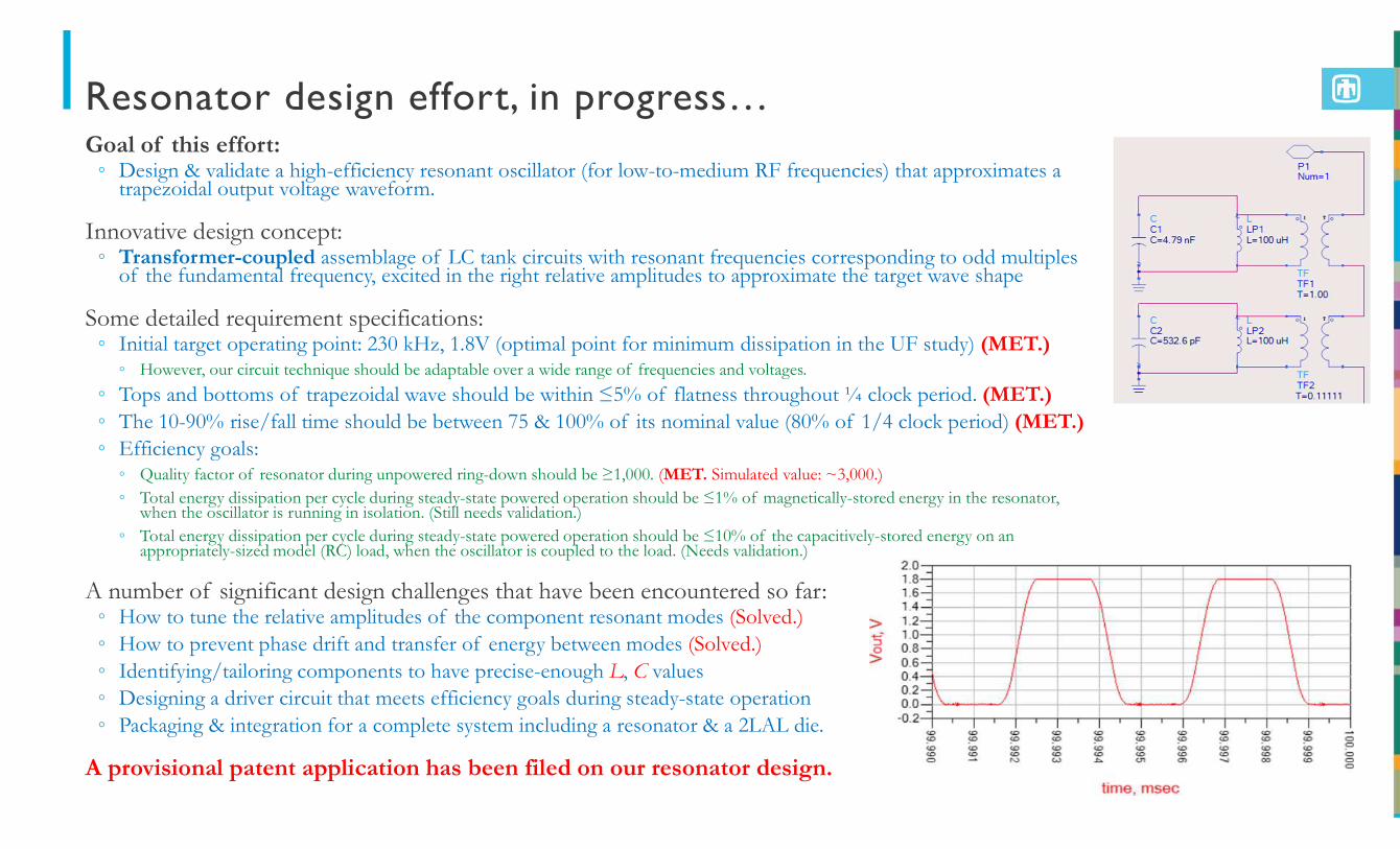
Resonator design effort, in progress…Goal of this effort: Design & validate a high-efficiency resonant oscillator (for low-to-medium RF frequencies) that approximates a
trapezoidal output voltage waveform.
Innovative design concept: Transformer-coupled assemblage of LC tank circuits with resonant frequencies corresponding to odd multiples
of the fundamental frequency, excited in the right relative amplitudes to approximate the target wave shape
Some detailed requirement specifications: Initial target operating point: 230 kHz, 1.8V (optimal point for minimum dissipation in the UF study) (MET.)
However, our circuit technique should be adaptable over a wide range of frequencies and voltages.
Tops and bottoms of trapezoidal wave should be within ≤5% of flatness throughout ¼ clock period. (MET.) The 10-90% rise/fall time should be between 75 & 100% of its nominal value (80% of 1/4 clock period) (MET.) Efficiency goals:
Quality factor of resonator during unpowered ring-down should be ≥1,000. (MET. Simulated value: ~3,000.) Total energy dissipation per cycle during steady-state powered operation should be ≤1% of magnetically-stored energy in the resonator,
when the oscillator is running in isolation. (Still needs validation.) Total energy dissipation per cycle during steady-state powered operation should be ≤10% of the capacitively-stored energy on an
appropriately-sized model (RC) load, when the oscillator is coupled to the load. (Needs validation.)
A number of significant design challenges that have been encountered so far: How to tune the relative amplitudes of the component resonant modes (Solved.) How to prevent phase drift and transfer of energy between modes (Solved.) Identifying/tailoring components to have precise-enough L, C values Designing a driver circuit that meets efficiency goals during steady-state operation Packaging & integration for a complete system including a resonator & a 2LAL die.
A provisional patent application has been filed on our resonator design.
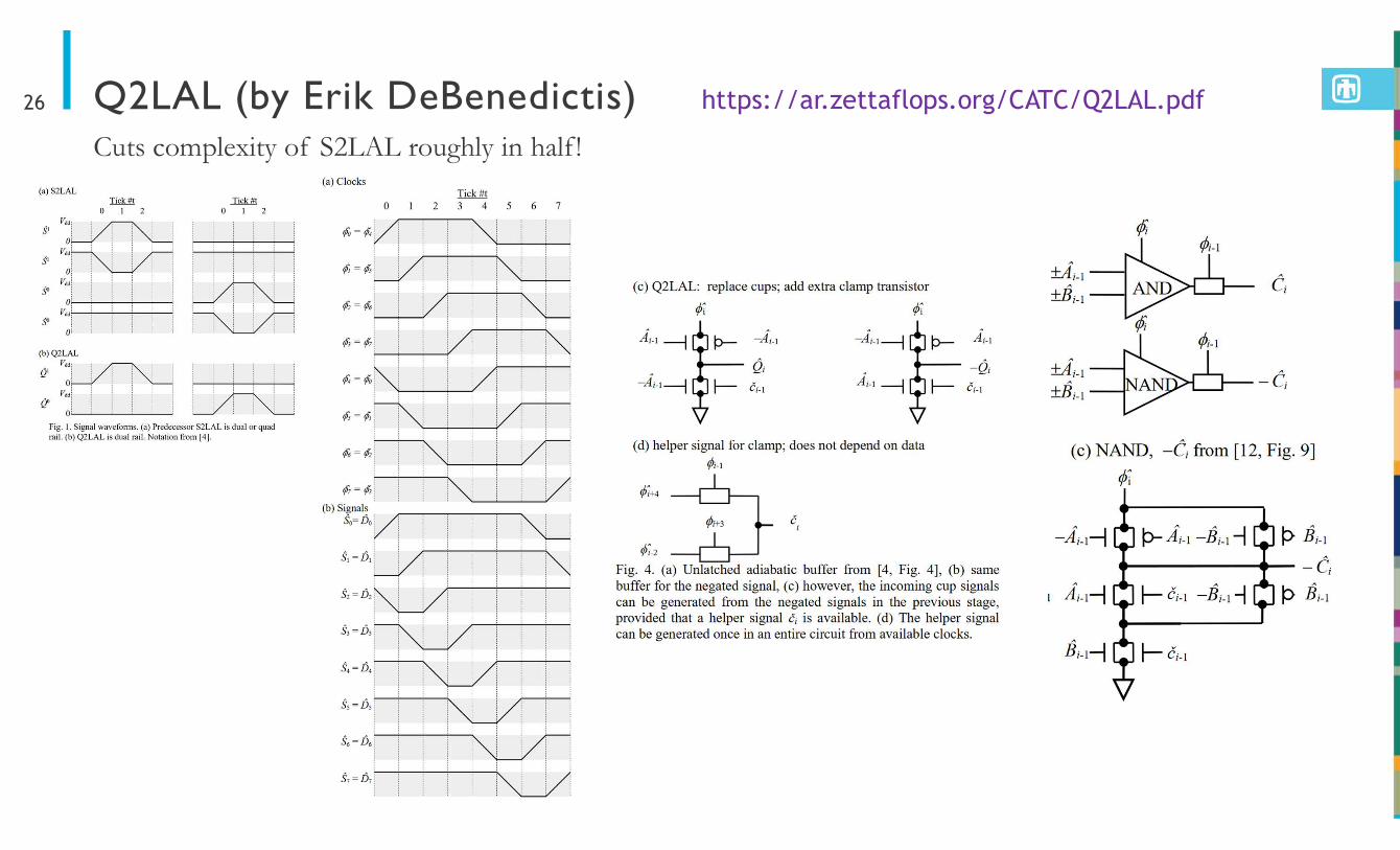
Q2LAL (by Erik DeBenedictis)Cuts complexity of S2LAL roughly in half!
26 https://ar.zettaflops.org/CATC/Q2LAL.pdf

Section IV. Future Work & Conclusion
Per fec t l y Ad iaba t i c CMOS Log ic
Future Work
Some next steps:1. Simulation studies.
Expect the minimum dissipation in realistic simulations to be lower than that of 2LAL.
2. Fabrication & power dissipation measurement of S2LAL test chips. Validate simulation results.
3. Open-source hardware. Open-source library of reference cells and example designs for static adiabatic CMOS.
Target an open PDK? (Sky130?)
4. Cryogenic technologies. Ultra-low dissipation. Steeper subthreshold slope, lower off-state current, re-optimize device structure to reduce gate leakage also.
Power supply decoupling. For cryo applications, can move the supply to the room-temperature environment.
Superconducting interconnects. Improves the energy-delay product due to reduced parasitic resistance.
5. High-Q resonant supplies. Currently under development at Sandia. (Provisional patent available under NDA.)
Superconducting versions are possible.
28
ConclusionWe have presented S2LAL, the first (and fastest!) form of fully static, fully adiabatic general sequential CMOS logic. We feel that these logic styles deserve the term “perfectly adiabatic.”
In principle, given a sufficiently low-leakage process, S2LAL should be capable of outperforming the energy efficiency of any other known semiconductor-based form of digital logic. S2LAL exhibits significant potential for both record-breaking scientific
demonstrations, as well as relatively near-term practical applications, particularly: Applications in cryogenic environments.
Any computing applications where energy efficiency is at a premium.
Also, S2LAL illustrates that vast gains in efficiency can still be achieved for general digital computing, even in CMOS, but onlyif we take the principles of reversible computing seriously, and develop implementations of them with care!
29
Acknowledgement: Thanks to Mr. Richard
Magnano for helping to inspire this innovation.
![Materi Luher Final€¦ · )x]]\ /rjlf 7uxwk 9doxhv %rrohdq /rjlf 7uxh )dovh +rz wr kdqgoh 8qfhuwdlq dqg 9djxhqhvv 3ureohpv")x]]\ /rjlf 7uxwk ydoxh lv d 'hjuhh ri 0hpehuvkls](https://img.pdfslide.us/doc/110x75/601c577c3396a606d663c123/materi-luher-final-x-rjlf-7uxwk-9doxhv-rrohdq-rjlf-7uxh-dovh-rz-wr-kdqgoh.jpg)