Embed Size (px)
Citation preview

Arasan Chip Systems Inc. 2010 North First Street, Suite #510, San Jose, CA 95131 Ph: 408-‐282-‐1600 Fax: 408-‐282-‐7800 www.arasan.com
Datasheet Gigabit Ethernet Total IP Solution

Datasheet
Copyright © 2015, Arasan Chip Systems Inc.
Disclaimer This document is written in good faith with the intent to assist the readers in the use of the product. Circuit diagrams and other information relating to Arasan Chip Systems’ products are included as a means of illustrating typical applications. Although the information has been checked and is believed to be accurate, no responsibility is assumed for inaccuracies. Information contained in this document is subject to continuous improvement and development.
Arasan Chip Systems’ products are not designed, intended, authorized or warranted for use in any life support or other application where product failure could cause or contribute to personal injury or severe property damage. Any and all such uses without prior written approval of an Officer of Arasan Chip Systems Inc. will be fully at the risk of the customer.
Arasan Chip Systems Inc. disclaims and excludes any and all warranties, including, without limitation, any and all implied warranties of merchantability, fitness for a particular purpose, title, and infringement and the like, and any and all warranties arising from any course or dealing or usage of trade.
This document may not be copied, reproduced, or transmitted to others in any manner. Nor may any use of information in this document be made, except for the specific purposes for which it is transmitted to the recipient, without the prior written consent of Arasan Chip Systems Inc. This specification is subject to change at any time without notice. Arasan Chip Systems Inc. is not responsible for any errors contained herein.
In no event shall Arasan Chip Systems Inc. be liable for any direct, indirect, incidental, special, punitive, or consequential damages; or for loss of data, profits, savings or revenues of any kind; regardless of the form of action, whether based on contract; tort; negligence of Arasan Chip Systems Inc or others; strict liability; breach of warranty; or otherwise; whether or not any remedy of buyers is held to have failed of its essential purpose, and whether or not Arasan Chip Systems Inc. has been advised of the possibility of such damages.
Restricted Rights
Use, duplication, or disclosure by the Government is subject to restrictions as set forth in FAR52.227-‐14 and DFAR252.227-‐7013 et seq. or its successor.
Copyright Notice
No part of this specification may be reproduced in any form or means, without the prior written consent of Arasan Chip Systems, Inc.
Questions or comments may be directed to:
Arasan Chip Systems Inc. 2010 North First Street, Suite 510 San Jose, CA 95131 Ph: 408-‐282-‐1600 Fax: 408-‐282-‐7800 Email: [email protected]

Datasheet
Copyright © 2015, Arasan Chip Systems Inc.
Contents
1 Introduction ...................................................................................................... 1 1.1 Arasan’s Ethernet Offerings ............................................................................................. 1 1.2 Total IP Solution ............................................................................................................... 1
2 Gigabit Ethernet MAC Controller ...................................................................... 3 2.1 Overview .......................................................................................................................... 3 2.2 Features ........................................................................................................................... 3 2.3 Architecture ..................................................................................................................... 4
2.3.1 Functional Block Diagram ............................................................................................... 4 2.3.2 Functional Block Diagram Description ............................................................................ 5
2.4 Pinout Diagrams .............................................................................................................. 7 2.4.1 Gigabit Ethernet – AHB IP Core Pinout Diagram ............................................................ 7 2.4.2 Signal Descriptions ......................................................................................................... 8 2.4.3 GEMAC-‐AXI PinOut Diagram ......................................................................................... 13 2.4.4 AXI Interface PinOut Description .................................................................................. 14 2.4.5 RGMII Interface ............................................................................................................ 20 2.4.6 GEMAC-‐AHB PinOut Block Diagram with RGMII Interface ........................................... 22 2.4.7 GEMAC-‐AXI PinOut Block Diagram with RGMII Interface ............................................. 23 2.4.8 RGMII Signal Description .............................................................................................. 24
2.5 SoC Level Integration ..................................................................................................... 26 2.5.1 Applications .................................................................................................................. 26 2.5.2 IP Deliverables .............................................................................................................. 26
3 10 Gigabit Ethernet MAC Controller ............................................................... 27 3.1 Overview ........................................................................................................................ 27 3.2 Features ......................................................................................................................... 27 3.3 Architecture ................................................................................................................... 28
3.3.1 Functional Block Diagram ............................................................................................. 28 3.3.2 Functional Block Diagram Description .......................................................................... 28
3.4 PinOut Diagrams ............................................................................................................ 31 3.4.1 XGMAC-‐AHB (XGMII32) PinOut Diagram ...................................................................... 31 3.4.2 XGMAC-‐AHB (XGMII64) PinOut Diagram ...................................................................... 32 3.4.3 XGMAC-‐AXI (XGMII32) PinOut Diagram ....................................................................... 33 3.4.4 XGMAC-‐AXI (XGMII64) PinOut Diagram ....................................................................... 34 3.4.5 XGMAC Pinout Descriptions ......................................................................................... 35
3.5 Signal Interfaces ............................................................................................................ 35 3.6 SoC Level Integration ..................................................................................................... 47
3.6.1 XGMAC Applications ..................................................................................................... 47 3.6.2 IP Deliverables .............................................................................................................. 48
Datasheet
Copyright © 2015, Arasan Chip Systems Inc.
4 Gigabit Ethernet with IEEE 1588 MAC Controller ............................................ 49 4.1 Introduction ................................................................................................................... 49 4.2 Overview ........................................................................................................................ 49 4.3 Features ......................................................................................................................... 50 4.4 Architecture ................................................................................................................... 51
4.4.1 Functional Block Diagram ............................................................................................. 51 4.4.2 Functional Block Diagram ............................................................................................. 51
4.5 PinOut Diagrams ............................................................................................................ 53 4.5.1 GEMAC-‐AHB Pinout Diagram ........................................................................................ 53 4.5.2 GEMAC-‐AXI Core Pin-‐ Out Diagram .............................................................................. 54 4.5.3 Pinout Descriptions ...................................................................................................... 55 4.5.4 Signal Interfaces ........................................................................................................... 55
4.6 SoC Level Integration ..................................................................................................... 67 4.6.1 Applications .................................................................................................................. 67 4.6.2 IP Deliverables .............................................................................................................. 68
5 Ethernet Device Driver .................................................................................... 69 5.1 Overview ........................................................................................................................ 69 5.2 Features ......................................................................................................................... 69 5.3 Description .................................................................................................................... 70 5.4 Deliverables ................................................................................................................... 70
6 Services & Support .......................................................................................... 71 6.1 Global Support ............................................................................................................... 71 6.2 Arasan Support Team .................................................................................................... 71 6.3 Professional Services & Customization .......................................................................... 71 6.4 The Arasan Porting Engine ............................................................................................ 71 6.5 Pricing & Licensing ......................................................................................................... 71
Tables Table 1: Gigabit Ethernet-‐AHB Core Pin-‐Out Description ..................................................................... 8 Table 2: M-‐RX Data Interface Signals .................................................................................................. 14 Table 3: AXI Target Interface Signals ................................................................................................... 18 Table 4: RGMII Signal Description ....................................................................................................... 24 Table 5: XGMII Interface Signal Description ........................................................................................ 36 Table 6: AHB Interface Signal Description ........................................................................................... 39 Table 7: AXI Interface Signal Description ............................................................................................ 40 Table 8: MII/GMII Interface Signal Description ................................................................................... 55 Table 9: AHB Interface Signal Description ........................................................................................... 58
Datasheet
Copyright © 2015, Arasan Chip Systems Inc.
Table 10: AXI Interface Signal Description .......................................................................................... 60 Table 11: 1588 Interface Signal Descriptions ...................................................................................... 66
Figures Figure 1: Arasan's Total IP Solution ....................................................................................................... 2 Figure 2: Gigabit Ethernet Core Block Diagram ..................................................................................... 4 Figure 3: Gigabit Ethernet-‐AHB Core Pinout Diagram ........................................................................... 7 Figure 4: GEMAC-‐AXI PinOut Diagram ................................................................................................ 13 Figure 5: GMII interface to RGMII interface signal mapping ............................................................... 21 Figure 6: Gigabit Ethernet-‐AHB Core Pinout Diagram with RGMII Interface ...................................... 22 Figure 7: GEMAC-‐AXI PinOut Diagram with RGMII Interface .............................................................. 23 Figure 8: Gigabit Ethernet-‐AHB core used in an SOC Implementation ............................................... 26 Figure 9: Gigabit Ethernet-‐AHB core Used in PCI/PCIExpress Network Interface Card ....................... 26 Figure 10: XGMAC Core Block Diagram ............................................................................................... 28 Figure 11: XGMAC-‐AHB (XGMII32) Core PinOut Diagram ................................................................... 31 Figure 12: XGMAC-‐AHB (XGMII64) Core PinOut Diagram ................................................................... 32 Figure 13: XGMAC-‐AXI (XGMII32) Core PinOut Diagram ..................................................................... 33 Figure 14: XGMAC-‐AXI (XGMII64) Core PinOut Diagram ..................................................................... 34 Figure 15: Core Configuration Signals ................................................................................................. 35 Figure 16: XGMAC Core used in PCIExpress based NIC Controller ...................................................... 47 Figure 17: XGMAC Core used Aggregation/Switch Device .................................................................. 47 Figure 18: GEMAC Core Block Diagram ............................................................................................... 51 Figure 19: GEMAC-‐AHB Pinout Diagram ............................................................................................. 53 Figure 20: GEMAC-‐ AXI Core Pin-‐ Out Diagram ................................................................................... 54 Figure 21: GEMAC Core in a SoC Application ...................................................................................... 67 Figure 22: GEMAC Core in an NIC Application .................................................................................... 67 Figure 23: Ethernet Device Driver ....................................................................................................... 70

Datasheet
Copyright © 2015, Arasan Chip Systems Inc. 1
1 Introduction 1.1 Arasan’s Ethernet Offerings Arasan Chip Systems has been shipping Ethernet IP for more than 10 years. The complete portfolio of Gigabit Ethernet products includes Gigabit (10/100/1000) Mbps and 10 Gigabit Ethernet MAC Controllers with support for AVB and IEEE 1588, Ethernet Driver, and Development Board for rapid integration into SoC and FPGA. The high quality IP has completed the rigorous interoperability tests at UNH-‐IOL laboratories and has been widely licensed. Licensees of Arasan’s Ethernet IP include companies such as Apple, Infineon Technologies, Ikanos Communications among others.
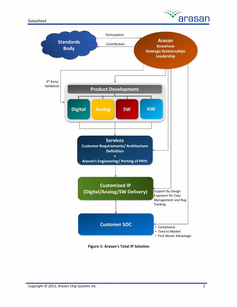
1.2 Total IP Solution Arasan’s Total IP Solution,encompasses all aspects of IP development and integration, including analog and digital IP cores, verification IP, software stacks & drivers, and hardware validation platforms. Benefits of Total IP Solution:
• Seamless integration from PHY to Software • Assured compliance across all components • Single point of support • Easiest acquisition process (one licensing source) • Lowest overall cost including cost of integration • Lowest risk for fast time to market
Datasheet
Copyright © 2015, Arasan Chip Systems Inc. 2
Figure 1: Arasan's Total IP Solution

Datasheet
Copyright © 2015, Arasan Chip Systems Inc. 3
2 Gigabit Ethernet MAC Controller 2.1 Overview The Arasan Gigabit Ethernet Media Access Controller IP is compliant with the Ethernet IEEE 802.3-‐2008 standard. The Gigabit Ethernet IP provides a 10/100 Mbps Media Independent Interface (MII) and a 1000 Mbps Gigabit Media Independent Interface (GMII). It also supports optional Reduced MII (RGMII), and Serial GMII (SGMII). The Gigabit Ethernet IP also implements Hardware assisted 1588 Protocol for Timestamping the Receive and Transmit PTP Packets. The Gigabit Ethernet IP is designed for SoC and mobile applications such as integrated networking devices, PCI-‐Express Ethernet controllers, and Ethernet adapter cards. The Gigabit Ethernet IP supports half-‐duplex mode at 10/100 Mbps and full-‐ duplex mode at 10/100/1000 Mbps.
The Gigabit Ethernet IP core consists of two configurable FIFOs on both transmits and receive sides to handle the application’s latency during frame transmission and reception. A processor bus master and a 32-‐bit scatter-‐gather DMA transfer packets between the internal FIFOs and the host memory to enhance system performance.
The Gigabit Ethernet IP supports 4-‐bit MII based 10/100 Mbps PHY and 8-‐bit GMII based 10/100/1000 Mbps PHY. A MDIO/MDC (Management Data Input/Output and Management Data Clock) management interface provides control and management functions to external PHY devices.
2.2 Features • Hardware Assisted 1588 V1/V2 Support • Full-‐duplex mode at 10/100/1000 Mbps • Half-‐duplex mode at 10/100 Mbps • Supports IEEE 802.3-‐2008 compliant MII, RMII, SMII, GMII, RGMII, and SGMII • Independent 32-‐bit scatter-‐gather DMA with big/ little endian operation • Optional VLAN Q-‐Tag frame support • CSMA/CD Protocol for half-‐duplex mode • PAUSE frame based flow control in full-‐duplex mode • MDIO/MDC management interface • 802.3 compliant MIB, SNMP, RMON management support • Configurable transmit and receive FIFOs • Supports Jumbo frames • Supports magic packet and Wake-‐Up frames • Optional AXI, AHB, PCIe, PCI or custom bus interface • Variable length Inter Frame Gap (IFG) on back to back frame transmission Variable length (3, 5,
7 bytes) preamble generation • Automatic generation of FCS and PAD • Option to disable PAD or CRC32 • Option to stop frame retransmission on collisions
Datasheet
Copyright © 2015, Arasan Chip Systems Inc. 4
• TimeStamps the specified PTP Packets for implementing 1588 Protocol • Inter Frame Gap checking • Preamble detection and stripping • Flexible address filtering modes and inverse address filtering 64-‐bit hash table to filter multicast
addresses • Promiscuous mode of operation • Reception of broadcast frames • Automatic checking the FCS field, runt frames, and data field length • Detection of MaxFrameLen frames, receive errors • 32-‐bit status information on each receive frame • Identifies PTP Frames (both V1 and/or V2) in L2/ L4 Encapsulation and TimeStamps for
implementing 1588 Protocol. • Software controlled PAUSE control frame generation including multicast and unicast address • Automatic detection and checking of PAUSE frames
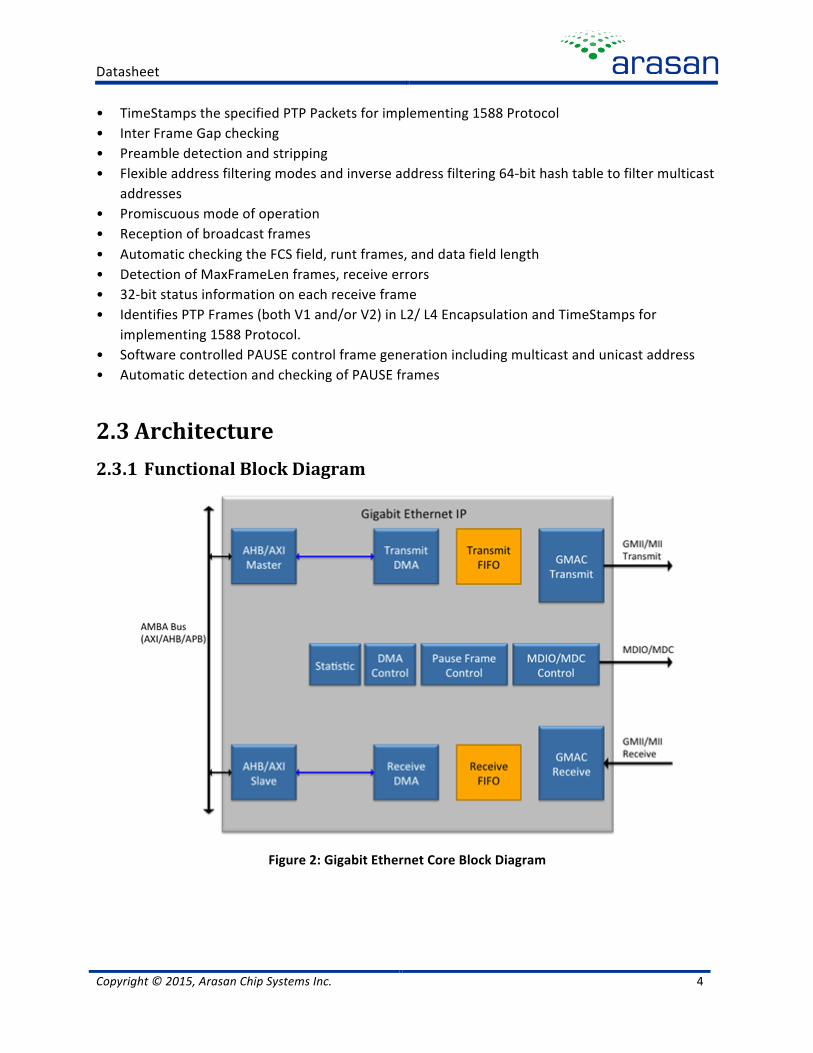
2.3 Architecture 2.3.1 Functional Block Diagram
Figure 2: Gigabit Ethernet Core Block Diagram
Datasheet
Copyright © 2015, Arasan Chip Systems Inc. 5
2.3.2 Functional Block Diagram Description
2.3.2.1 AHB/AXI Master
This module provides the AHB/AXI Master functionality to generate transactions on the AHB/AXI Bus. The transactions are generated based on the requests from the Transmit/Receive DMA’s.
2.3.2.2 AHB/AXI Slave (Target)
This module provides the AHB/AXI Target functionality to the AHB/AXI Host (CPU). This interface is used to access all the DMA/MAC registers in the Registers Module.
2.3.2.3 TX _DMA
This module implements the Transmit DMA to transfer the frames from the Host Memory to the Transmit FIFO using the Transmit Descriptors.
2.3.2.4 EMAC_TXFIFO
This module has a configurable FIFO to store the Frames that are received from the Host memory before the frames are transferred onto Ethernet Interface. This module also has additional FIFO control logic that helps in frame retransmission during Collisions.
2.3.2.5 EMAC_TX
This module implements the Frame Transmit State Machine of the CSMA/CD protocol by transmitting frames onto either MII or GMII Interface based on the Speed.
2.3.2.6 DMA_CSR
This module implements the Control and Status Registers to control the operation of Receive and Transmit DMA and also the Receive and Transmit operations of the Ethernet Interface. This module also provides access to the Statistics Counters and provides interrupt/status information to the AHB Host.
2.3.2.7 STATISTICS
This module maintains various counters to perform Statistics for both Transmit and Receive operation
2.3.2.8 PAUSE_FC
This module decodes the Pause Frames received when the EMAC Core is in Full Duplex Mode and implements the PAUSE_TIMER to disable the EMAC_TX module. Also this module generates Pause Frames on Software request
2.3.2.9 2.9 MDC/MDIO Controller
This module generates MDIO Frames to talk to external PHY Devices

Datasheet
Copyright © 2015, Arasan Chip Systems Inc. 6
2.3.2.10 RX_DMA
This module implements the Receive DMA to transfer the frames from the Internal FIFO to the Host Memory using the Receive Descriptors
2.3.2.11 EMAC_RXFIFO
This module has a configurable FIFO to store the received frames before they are transferred to the Host memory. This module also has additional control logic to flush error packets from the FIFO.
2.3.2.12 EMAC_RX
This module implements the Frame Receive State Machine of the CSMA/CD Protocol by receiving frames from MII/GMII Interface and performing field extraction and error checking.
2.3.2.13 AHB/AXI Master Interface
The AHB Master Interface (32-‐bit or 64-‐bit) is used for bus mastering capability on the AHB Bus by the GEMAC Core. The core generates transactions on this interface to transfer frame data between the Host memory and the internal FIFO’s. Using this interface the descriptors are transferred.
2.3.2.14 AHB/AXI Slave (Target) Interface
The AHB or AXI Target (also called as Slave) Interface provides a 32-‐bit data interface to read/write the internal registers in the GEMAC Core.
2.3.2.15 MII/GMII Interface
The GEMAC Core interfaces to the external PHY device using the IEEE802.3 compliant GMII/MII Interface. In case of 10/100 Mbps, the MII Interface (4-‐bit wide) is used and when operating in 1000 Mbps mode, the GMII Interface (8-‐bit wide) is used. This interface is specified in the IEEE 802.3 specification. Any of the Standard Ethernet PHY Controller Chips can be hooked onto this interface for connecting to the Ethernet Cable
2.3.2.16 MDC/MDIO Interface
This is a 2-‐wire interface that is used to configure and control an external IEEE802.3 Compliant PHY device using the MII Management Frame structure. The interface is defined in the IEEE802.3 Specification.
2.3.2.17 SGMII/RGMII Interface
The GEMAC Core optionally supports Reduced GMII (RGMII) and Serial GMII (SGMII) Interfaces to reduce the pin count on the Ethernet Interface.
Datasheet
Copyright © 2015, Arasan Chip Systems Inc. 7
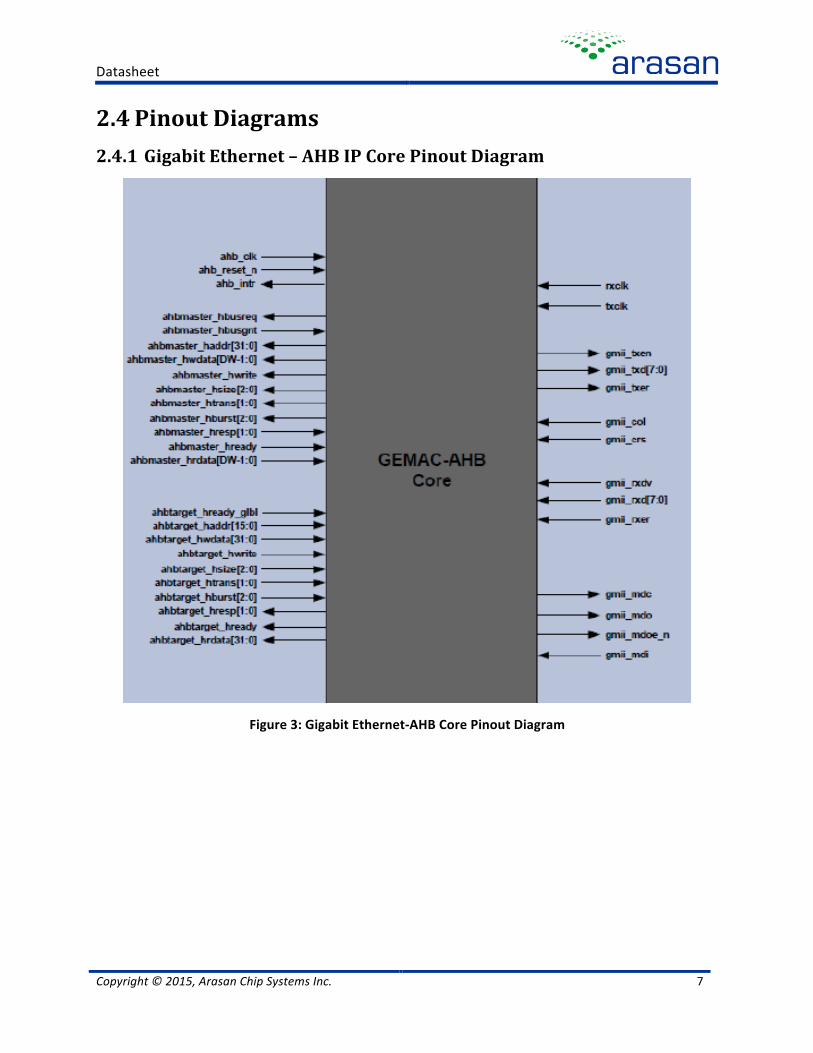
2.4 Pinout Diagrams 2.4.1 Gigabit Ethernet – AHB IP Core Pinout Diagram
Figure 3: Gigabit Ethernet-‐AHB Core Pinout Diagram
Datasheet
Copyright © 2015, Arasan Chip Systems Inc. 8
2.4.2 Signal Descriptions The following table describes each of the Gigabit Ethernet-‐AHB signals in detail. All signals are active high unless specified. Active low signals are suffixed with “_n”
• All signals that Interface to the MII/GMII interface are prefixed with “gmii_” • All signals that Interface to the AHB master Interface are prefixed with “ahbmaster_” • All signals that Interface to the AHB slave Interface are prefixed with “ahbtarget_”
Table 1: Gigabit Ethernet-‐AHB Core Pin-‐Out Description
Signal Name I/O Description
MII/GMII Interface
txclk Input txclk (MII/GMII Transmit Clock) is a continuous clock that provides for the timing reference for the transfer of the gmii_txen, gmii_txer, and gmii_txd[7:0] signals from the Gigbit Ethernet-‐AHB Core to the Ethernet PHY Controller. In the MII Mode the txclk is sourced by the External Ethernet PHY Controller chip. The operating frequency of the txclk is 25 MHz when operating at 100-‐Mb/s and 2.5 MHz when operating at 10-‐Mb/s. In the GMII Mode the txclk is sourced from the Application. Also this is sent out as gmii_txclk. The operating frequency of the txclk is 125 MHz in this mode. A Clock mux is required to multiplex the 125 Mhz (for 1000 Mbps) Clock and MII_TXCLK (for 10/100 Mbps) outside of the Core.
gmii_txd[7:0] Output gmii_txd[7:0] (GMII/MII Transmit Data) is driven by the Gigabit Ethernet-‐AHB Core to the External PHY Controller/PCS Module. gmii_txd will transition synchronously with respect to the txclk. For each txclk period in which gmii_txen is asserted, gmii_txd will have the data to be accepted by the Ethernet PHY Controller chip/PCS Module. gmii_txd[0] is the least significant bit. While gmii_txen is de-‐asserted the data presented on gmii_txd should be ignored. When the Gigbit Ethernet-‐AHB is operating in MII Mode (10/ 100 Mbps), only the lower 4 bits (gmii_txd[3:0]) are used to drive the data.
gmmi_txen Output gmii_txen (GMII/MII Transmit Enable) indicates that the Gigbit Ethernet-‐AHB Core is presenting data on the GMII/MII for transmission. It will be asserted by the Gigbit Ethernet-‐AHB Core with the first byte/nibble of the preamble and will remain asserted while all data to be transmitted are presented on the GMII/MII Interface. gmii_txen will be negated prior to the first clock following the final byte/nibble of the frame. gmii_txen is driven by the Gigbit Ethernet-‐AHB Core and will
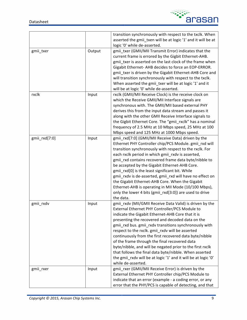
Datasheet
Copyright © 2015, Arasan Chip Systems Inc. 9
transition synchronously with respect to the txclk. When asserted the gmii_txen will be at logic '1' and it will be at logic '0' while de-‐asserted.
gmii_txer Output gmii_txer (GMII/MII Transmit Error) indicates that the current frame is errored by the Gigbit Ethernet-‐AHB. gmii_txer is asserted on the last clock of the frame when Gigabit Ethernet-‐ AHB decides to force an EOP-‐ERROR. gmii_txer is driven by the Gigabit Ethernet-‐AHB Core and will transition synchronously with respect to the txclk. When asserted the gmii_txer will be at logic '1' and it will be at logic '0' while de-‐asserted.
rxclk Input rxclk (GMII/MII Receive Clock) is the receive clock on which the Receive GMII/MII Interface signals are synchronous with. The GMII/MII based external PHY derives this from the input data stream and passes it along with the other GMII Receive Interface signals to the Gigbit Ethernet Core. The “gmii_rxclk” has a nominal frequency of 2.5 MHz at 10 Mbps speed, 25 MHz at 100 Mbps speed and 125 MHz at 1000 Mbps speed.
gmii_rxd[7:0] Input gmii_rxd[7:0] (GMII/MII Receive Data) driven by the Ethernet PHY Controller chip/PCS Module. gmii_rxd will transition synchronously with respect to the rxclk. For each rxclk period in which gmii_rxdv is asserted, gmii_rxd contains recovered frame data byte/nibble to be accepted by the Gigabit Ethernet-‐AHB Core. gmii_rxd[0] is the least significant bit. While gmii_rxdv is de-‐asserted, gmii_rxd will have no effect on the Gigabit Ethernet-‐AHB Core. When the Gigabit Ethernet-‐AHB is operating in MII Mode (10/100 Mbps), only the lower 4 bits (gmii_rxd[3:0]) are used to drive the data.
gmii_rxdv
Input gmii_rxdv (MII/GMII Receive Data Valid) is driven by the External Ethernet PHY Controller/PCS Module to indicate the Gigabit Ethernet-‐AHB Core that it is presenting the recovered and decoded data on the gmii_rxd bus. gmii_rxdv transitions synchronously with respect to the rxclk. gmii_rxdv will be asserted continuously from the first recovered data byte/nibble of the frame through the final recovered data byte/nibble, and will be negated prior to the first rxclk that follows the final data byte/nibble. When asserted the gmii_rxdv will be at logic ’1’ and it will be at logic ’0’ while de-‐asserted.
gmii_rxer
Input gmii_rxer (GMII/MII Receive Error) is driven by the External Ethernet PHY Controller chip/PCS Module to indicate that an error (example -‐ a coding error, or any error that the PHY/PCS is capable of detecting, and that
Datasheet
Copyright © 2015, Arasan Chip Systems Inc. 10
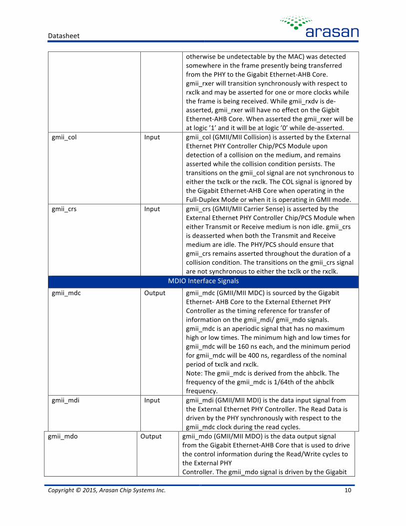
otherwise be undetectable by the MAC) was detected somewhere in the frame presently being transferred from the PHY to the Gigabit Ethernet-‐AHB Core. gmii_rxer will transition synchronously with respect to rxclk and may be asserted for one or more clocks while the frame is being received. While gmii_rxdv is de-‐asserted, gmii_rxer will have no effect on the Gigbit Ethernet-‐AHB Core. When asserted the gmii_rxer will be at logic ’1’ and it will be at logic ’0’ while de-‐asserted.
gmii_col
Input gmii_col (GMII/MII Collision) is asserted by the External Ethernet PHY Controller Chip/PCS Module upon detection of a collision on the medium, and remains asserted while the collision condition persists. The transitions on the gmii_col signal are not synchronous to either the txclk or the rxclk. The COL signal is ignored by the Gigabit Ethernet-‐AHB Core when operating in the Full-‐Duplex Mode or when it is operating in GMII mode.
gmii_crs
Input gmii_crs (GMII/MII Carrier Sense) is asserted by the External Ethernet PHY Controller Chip/PCS Module when either Transmit or Receive medium is non idle. gmii_crs is deasserted when both the Transmit and Receive medium are idle. The PHY/PCS should ensure that gmii_crs remains asserted throughout the duration of a collision condition. The transitions on the gmii_crs signal are not synchronous to either the txclk or the rxclk.
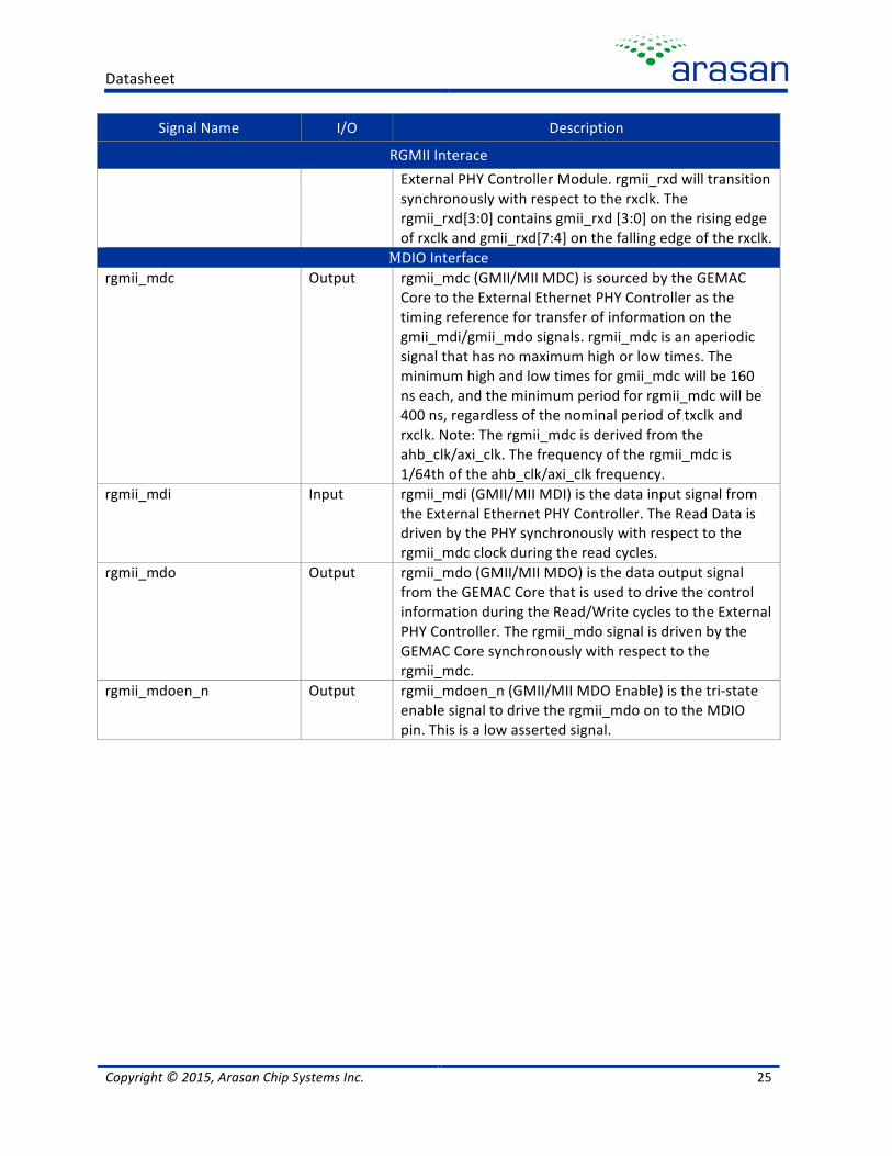
MDIO Interface Signals
gmii_mdc
Output gmii_mdc (GMII/MII MDC) is sourced by the Gigabit Ethernet-‐ AHB Core to the External Ethernet PHY Controller as the timing reference for transfer of information on the gmii_mdi/ gmii_mdo signals. gmii_mdc is an aperiodic signal that has no maximum high or low times. The minimum high and low times for gmii_mdc will be 160 ns each, and the minimum period for gmii_mdc will be 400 ns, regardless of the nominal period of txclk and rxclk. Note: The gmii_mdc is derived from the ahbclk. The frequency of the gmii_mdc is 1/64th of the ahbclk frequency.
gmii_mdi
Input gmii_mdi (GMII/MII MDI) is the data input signal from the External Ethernet PHY Controller. The Read Data is driven by the PHY synchronously with respect to the gmii_mdc clock during the read cycles.
gmii_mdo
Output gmii_mdo (GMII/MII MDO) is the data output signal from the Gigabit Ethernet-‐AHB Core that is used to drive the control information during the Read/Write cycles to the External PHY Controller. The gmii_mdo signal is driven by the Gigabit

Datasheet
Copyright © 2015, Arasan Chip Systems Inc. 11
Ethernet-‐AHB Core synchronously with respect to the gmii_mdc.
gmii_mdoen_n
Output gmii_mdoen_n (GMII/MII MDO Enable) is the tri-‐state enable signal to drive the gmii_mdo on to the MDIO pin. This is a low asserted signal.
AHB Master Interface Signals
ahbclk
Input ahbclk (AHB Clock) is the system clock on which both the AHB Master Interface and AHB slave Interface is synchronous to.
ahbreset_n
Input ahbreset_n (AHB Reset) is the System Reset to reset the Gigabit Ethernet-‐AHB Core to the default State. This is an active low signal. When asserted, this signal must be asserted for at least 64 Clock cycles.
ahb_intr Output Interrupt Output to the AHB Bus ahbmaster_hbusreq Output Bus Request on the AHB Master Interface. ahbmaster_hgrant Input Bus Grant on the AHB Master Interface. ahbmaster_haddr[31:0]
Output Bus Address on the AHB Master Interface. This is a Byte Addressable Address.
ahbmaster_hwdata[31:0] Output Write Data on the AHB Master Interface.
ahbmaster_hrdata[31:0]
Input Read Data on the AHB Master Interface.
ahbmaster_hwrite
Output Write or Read Direction Indication for the current AHB Master transaction. 1’b1: Write 1’b0: Read
ahbmaster_hsize[2:0] Output Size of the Data width.
ahbmaster_htrans[1:0
Output Transfer Type
ahbmaster_hburst[2:0]
Output Burst Size
ahbmaster_hready_glbl
Input Global Ready
ahbmaster_hresp[1:0]
Input Transfer Response
ahbmaster_intr
Output Interrupt Output to the AHB Bus.
AHB Slave Interface Signals
ahbtarget_haddr[15:0] Input Bus Address on the AHB slave Interface. This is a Byte Addressable Address. • Only 16-‐bits of the Address are used. • All Registers in the Gigabit Ethernet-‐AHB Core are
32-‐bit aligned. ahbtarget_hwdata[31:0] Input Write Data on the AHB slave Interface.
Datasheet
Copyright © 2015, Arasan Chip Systems Inc. 12
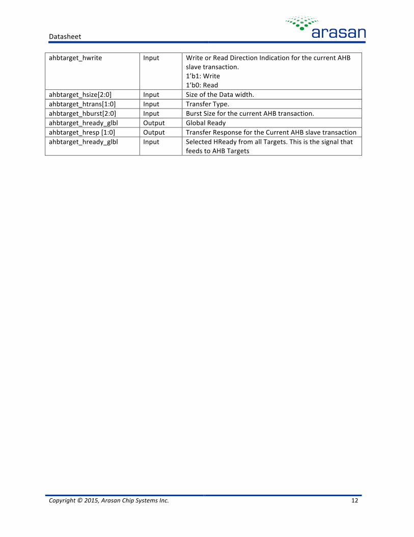
ahbtarget_hwrite Input Write or Read Direction Indication for the current AHB slave transaction. 1’b1: Write 1’b0: Read
ahbtarget_hsize[2:0] Input Size of the Data width. ahbtarget_htrans[1:0] Input Transfer Type. ahbtarget_hburst[2:0] Input Burst Size for the current AHB transaction. ahbtarget_hready_glbl Output Global Ready ahbtarget_hresp [1:0] Output Transfer Response for the Current AHB slave transaction ahbtarget_hready_glbl Input Selected HReady from all Targets. This is the signal that
feeds to AHB Targets

Datasheet
Copyright © 2015, Arasan Chip Systems Inc. 13
2.4.3 GEMAC-‐AXI PinOut Diagram
Figure 4: GEMAC-‐AXI PinOut Diagram

Datasheet
Copyright © 2015, Arasan Chip Systems Inc. 14
2.4.4 AXI Interface PinOut Description The following table describes each of the GEMAC Signal in detail. All signals are active high unless specified.
• Active low signals are suffixed with “_n”. • All signals that Interface to the MII/GMII Interface are prefixed with “gmii_”. • The AHB Clock/Reset/Interrupt signals (when AHB Interface is used) are prefixed with “ahb_” • All signals that Interface to the AHB Master Interface (when AHB Interface is used) are prefixed
with “ahbmaster_” • All signals that Interface to the AHB Target Interface (when AHB Interface is used) are prefixed
with“ahbtarget_” • The AXI Clock/Reset/Interrupt signals (when AHB Interface is used) are prefixed with • “axi_” • All signals that Interface to the AXI Master Interface (when AXI Interface is used) are prefixed
with “aximst_” • All signals that Interface to the AXI Slave (Target) Interface (when AXI Interface is used) are
prefixed with “axislv_”
Table 2: M-‐RX Data Interface Signals
Signal Direction Description
AXI Clock/Reset/Interrupt Signals
axi_clk Input axi_clk (AXI Clock) is the system clock on which both the AXI Master Interface and AXI Slave (Target) Interface is synchronous to.
axi_reset_n Input axi_reset_n (AXI Reset) is the System Reset to reset the GEMAC Core to the default State. This is an active low signal. When asserted, this signal must be asserted for at least 64 Clock cycles.
axi_intr Output Interrupt Output to the AXI Bus AXI Master Inter
aximst_awid[3:0] Output Write address ID. This signal is the identification tag for the write address group of signals.
aximst_awaddr[31:0]
Output Write address. The write address bus gives the address of the first transfer in a write burst transaction. The associated control signals are used to determine the addresses of the remaining transfers in the burst.
aximst_awlen[3:0]
Output Burst length. The burst length gives the exact number of transfers in a burst. This information determines the number of data transfers associated with the address. Refer to AMBA Specification for encoding of this field.
aximst_awsize[2:0] Output Burst size. This signal indicates the size of each transfer in the burst. Byte lane strobes indicate exactly which byte lanes to update.
Datasheet
Copyright © 2015, Arasan Chip Systems Inc. 15
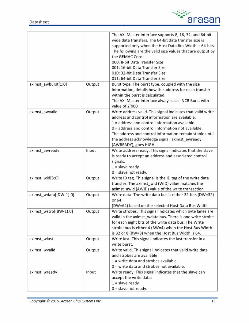
The AXI Master interface supports 8, 16, 32, and 64-‐bit wide data transfers. The 64-‐bit data transfer size is supported only when the Host Data Bus Width is 64-‐bits. The following are the valid size values that are output by the GEMAC Core. 000: 8-‐bit Data Transfer Size 001: 16-‐bit Data Transfer Size 010: 32-‐bit Data Transfer Size 011: 64-‐bit Data Transfer Size.
aximst_awburst[1:0] Output Burst type. The burst type, coupled with the size information, details how the address for each transfer within the burst is calculated. The AXI Master interface always uses INCR Burst with value of 2’b00
aximst_awvalid Output Write address valid. This signal indicates that valid write address and control information are available: 1 = address and control information available 0 = address and control information not available. The address and control information remain stable until the address acknowledge signal, aximst_awready (AWREADY), goes HIGH.
aximst_awready
Input Write address ready. This signal indicates that the slave is ready to accept an address and associated control signals: 1 = slave ready 0 = slave not ready.
aximst_wid[3:0] Output Write ID tag. This signal is the ID tag of the write data transfer. The aximst_wid (WID) value matches the aximst_awid (AWID) value of the write transaction
aximst_wdata[(DW-‐1):0] Output Write data. The write data bus is either 32-‐bits (DW=32) or 64 (DW=64) based on the selected Host Data Bus Width
aximst_wstrb[(BW-‐1):0] Output Write strobes. This signal indicates which byte lanes are valid in the aximst_wdata bus. There is one write strobe for each eight bits of the write data bus. The Write strobe bus is either 4 (BW=4) when the Host Bus Width is 32 or 8 (BW=8) when the Host Bus Width is 64.
aximst_wlast Output Write last. This signal indicates the last transfer in a write burst.
aximst_wvalid Output Write valid. This signal indicates that valid write data and strobes are available: 1 = write data and strobes available 0 = write data and strobes not available.
aximst_wready
Input Write ready. This signal indicates that the slave can accept the write data: 1 = slave ready 0 = slave not ready.

Datasheet
Copyright © 2015, Arasan Chip Systems Inc. 16
aximst_bid[3:0] Input Response ID. The identification tag of the write response. The aximst_bid (BID) value must match the aximst_awid (AWID) value of the write transaction to which the slave is responding.
aximst_bresp[1:0] I Input Write response. This signal indicates the status of the write transaction. The allowable responses are as follows: 2’b00 -‐ OKAY 2’b01 -‐ EXOKAY 2’b10 -‐ SLVERR 2’b11 -‐ DECERR. The Response EXOKAY should never be asserted as the Master never generates Exclusive access.
aximst_bvalid Input Write response valid. This signal indicates that a valid write response is available: 1 = write response available 0 = write response not available.
aximst_bready Output Response ready. This signal indicates that the GEMAC Core can accept the response information. 1 = master ready 0 = master not ready.
AXI Master Read Interface Signals aximst_arid[3:0] Output Read address ID. This signal is the identification tag for
the write address group of signals. aximst_araddr[31:0] Output Read address. The read address bus gives the address of
the first transfer in a read burst transaction. The associated control signals are used to determine the addresses of the remaining transfers in the burst.
aximst_arlen[3:0] Output Burst length. The burst length gives the exact number of transfers in a burst. This information determines the number of data transfers associated with the address. Refer to AMBA Specification for encoding of this field.
aximst_arsize[2:0] Output Burst size. This signal indicates the size of each transfer in the burst. Byte lane strobes indicate exactly which byte lanes to update. The AXI Master interface supports 8, 16, 32, and 64-‐bit wide data transfers. The 64-‐bit data transfer size is supported only when the Host Data Bus Width is 64-‐bits. The following are the valid size values that are output by the GEMAC Core. 000: 8-‐bit Data Transfer Size 001: 16-‐bit Data Transfer Size 010: 32-‐bit Data Transfer Size 011: 64-‐bit Data Transfer Size
aximst_arburst[1:0]
Output Burst type. The burst type, coupled with the size information, details how the address for each transfer within the burst is calculated. The AXI Master interface

Datasheet
Copyright © 2015, Arasan Chip Systems Inc. 17
always uses INCR Burst with value of 2’b00. aximst_arvalid Output Read address valid. This signal indicates that valid read
address and control information are available: 1 = address and control information available 0 = address and control information not available. The address and control information remain stable until the address acknowledge signal, aximst_arready (ARREADY), goes HIGH.
aximst_arready Input Read address ready. This signal indicates that the slave is ready to accept an address and associated control signals: 1 = slave ready 0 = slave not ready.
aximst_rid[3:0] Input Read ID tag. This signal is the ID tag of the read data transfer. The aximst_rid (RID) value matches the aximst_arid (ARID) value of the read transaction.
aximst_rdata[(DW-‐1):0] Input Read data. The read data bus is either 32-‐bits (DW=32) or 64 (DW=64) based on the selected Host Data Bus Width.
aximst_rresp[1:0] Input Read response. This signal indicates the status of the read transaction. The allowable responses are as follows: 2’b00 -‐ OKAY 2’b01 -‐ EXOKAY 2’b10 -‐ SLVERR 2’b11 -‐ DECERR. The Response EXOKAY should never be asserted as the Master never generates Exclusive access.
aximst_rlast Input Read last. This signal indicates the last transfer in a read burst.
aximst_rvalid Input Read valid. This signal indicates that valid read data and strobes are available: 1 = read data and strobes available 0 = read data and strobes not available.
aximst_rready Output Read ready. This signal indicates that the GEMAC Core can accept the read data: 1 = slave ready 0 = slave not ready.
Datasheet
Copyright © 2015, Arasan Chip Systems Inc. 18
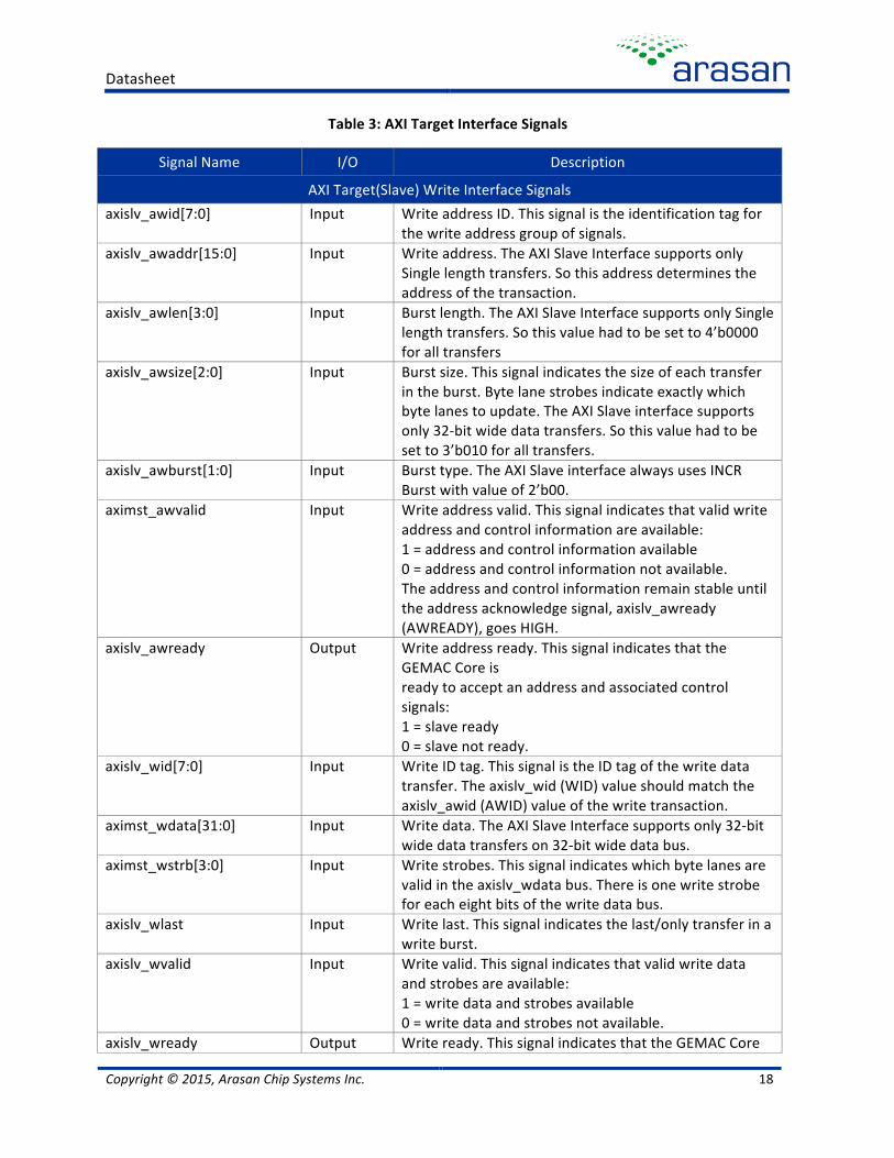
Table 3: AXI Target Interface Signals
Signal Name I/O Description
AXI Target(Slave) Write Interface Signals axislv_awid[7:0] Input Write address ID. This signal is the identification tag for
the write address group of signals. axislv_awaddr[15:0] Input Write address. The AXI Slave Interface supports only
Single length transfers. So this address determines the address of the transaction.
axislv_awlen[3:0] Input Burst length. The AXI Slave Interface supports only Single length transfers. So this value had to be set to 4’b0000 for all transfers
axislv_awsize[2:0] Input Burst size. This signal indicates the size of each transfer in the burst. Byte lane strobes indicate exactly which byte lanes to update. The AXI Slave interface supports only 32-‐bit wide data transfers. So this value had to be set to 3’b010 for all transfers.
axislv_awburst[1:0] Input Burst type. The AXI Slave interface always uses INCR Burst with value of 2’b00.
aximst_awvalid Input Write address valid. This signal indicates that valid write address and control information are available: 1 = address and control information available 0 = address and control information not available. The address and control information remain stable until the address acknowledge signal, axislv_awready (AWREADY), goes HIGH.
axislv_awready Output Write address ready. This signal indicates that the GEMAC Core is ready to accept an address and associated control signals: 1 = slave ready 0 = slave not ready.
axislv_wid[7:0] Input Write ID tag. This signal is the ID tag of the write data transfer. The axislv_wid (WID) value should match the axislv_awid (AWID) value of the write transaction.
aximst_wdata[31:0] Input Write data. The AXI Slave Interface supports only 32-‐bit wide data transfers on 32-‐bit wide data bus.
aximst_wstrb[3:0] Input Write strobes. This signal indicates which byte lanes are valid in the axislv_wdata bus. There is one write strobe for each eight bits of the write data bus.
axislv_wlast Input Write last. This signal indicates the last/only transfer in a write burst.
axislv_wvalid Input Write valid. This signal indicates that valid write data and strobes are available: 1 = write data and strobes available 0 = write data and strobes not available.
axislv_wready Output Write ready. This signal indicates that the GEMAC Core

Datasheet
Copyright © 2015, Arasan Chip Systems Inc. 19
Signal Name I/O Description
AXI Target(Slave) Write Interface Signals can accept the write data: 1 = slave ready 0 = slave not ready.
axislv_bid[7:0] Output Response ID. The identification tag of the write response. The axislv_bid (BID) value matches the axislv_awid (AWID) value of the write transaction to which the slave is responding.
axislv_bresp[1:0] Output Write response. This signal indicates the status of the write transaction. The allowable responses are as follows: 2’b00 -‐ OKAY 2’b01 -‐ EXOKAY 2’b10 -‐ SLVERR 2’b11 -‐ DECERR. The Response EXOKAY will never be asserted as the Slave does not support Exclusive access.
axislv_bvalid Output Write response valid. This signal indicates that a valid write response is available: 1 = write response available 0 = write response not available
axislv_bready Input Response ready. This signal indicates that the master can accept the response information. 1 = master ready 0 = master not ready.
AXI Target(Slave) Read Interface Signals axislv_arid[7:0] Input Read address ID. This signal is the identification tag for
the write address group of signals araddr[15:0] Input Read address. The AXI Slave Interface supports only
Single length transfers. So this address determines the address of the transaction.
axislv_arlen[3:0] Input Burst length. The AXI Slave Interface supports only Single length transfers. So this value had to be set to 4’b0000 for all transfers.
axislv_arsize[2:0] Input Burst size. This signal indicates the size of each transfer in the burst. Byte lane strobes indicate exactly which byte lanes to update. The AXI Slave interface supports only 32-‐bit wide data transfers. So this value had to be set to 3’b010 for all transfers.
axislv_arburst[1:0] Input Burst type. The AXI Slave interface always uses INCR Burst with value of 2’b00.
axislv_arvalid Input Read address valid. This signal indicates that valid write address and control information are available: 1 = address and control information available 0 = address and control information not available.

Datasheet
Copyright © 2015, Arasan Chip Systems Inc. 20
Signal Name I/O Description
AXI Target(Slave) Write Interface Signals The address and control information remain stable until the address acknowledge signal, axislv_arready (ARREADY), goes HIGH.
axislv_arready Output Write address ready. This signal indicates that the GEMAC Core is ready to accept an address and associated control signals: 1 = slave ready 0 = slave not ready.
axislv_rid[7:0] Output Read ID tag. This signal is the ID tag of the read data transfer. The axislv_rid (RID) value matches the axislv_arid (ARID) value of the read transaction
aximst_rdata[31:0] Output Read data. The AXI Slave Interface supports only 32-‐bit wide data transfers on 32-‐bit wide data bus.
axislv_rresp[1:0] Output Read response. This signal indicates the status of the read transaction. The allowable responses are as follows: 2’b00 -‐ OKAY 2’b01 -‐ EXOKAY 2’b10 -‐ SLVERR 2’b11 -‐ DECERR. The Response EXOKAY should never be asserted as the Master never generates Exclusive access.
axislv_rlast Output Read last. This signal indicates the last transfer in a read burst.
axislv_rvalid Output Read valid. This signal indicates that valid read data and strobes are available: 1 = read data and strobes available 0 = read data and strobes not available.
axislv_rready Input Read ready. This signal indicates that the Master can accept the read data: 1 = slave ready 0 = slave not ready.
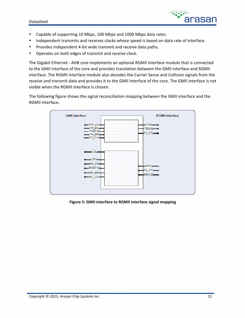
2.4.5 RGMII Interface The Gigabit Ethernet -‐ AHB core can optionally support Reduced GMII (RGMII) interface, that is compliant with “RGMII Specification Rev 1.3”, to reduce the pin count on the GMII interface. The GMII interface comprises of 25 pins for data and control signals. The RGMII interface has four bit wide data-‐path along with one bit control for each transmit and receive direction resulting in a total of 12 pins. The MDC/MDIO interface is unaffected by the RGMII interface. The RGMII interface has the following characteristics:
Datasheet
Copyright © 2015, Arasan Chip Systems Inc. 21
• Capable of supporting 10 Mbps, 100 Mbps and 1000 Mbps data rates. • Independent transmits and receives clocks whose speed is based on data rate of interface. • Provides independent 4-‐bit wide transmit and receive data paths. • Operates on both edges of transmit and receive clock.
The Gigabit Ethernet -‐ AHB core implements an optional RGMII interface module that is connected to the GMII interface of the core and provides translation between the GMII interface and RGMII interface. The RGMII interface module also decodes the Carrier Sense and Collision signals from the receive and transmit data and provides it to the GMII Interface of the core. The GMII interface is not visible when the RGMII interface is chosen.
The following figure shows the signal reconciliation mapping between the GMII interface and the RGMII interface.
Figure 5: GMII interface to RGMII interface signal mapping

Datasheet
Copyright © 2015, Arasan Chip Systems Inc. 22
2.4.6 GEMAC-‐AHB PinOut Block Diagram with RGMII Interface
Figure 6: Gigabit Ethernet-‐AHB Core Pinout Diagram with RGMII Interface
Datasheet
Copyright © 2015, Arasan Chip Systems Inc. 23
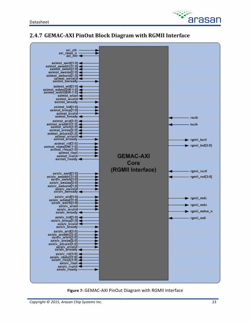
2.4.7 GEMAC-‐AXI PinOut Block Diagram with RGMII Interface
Figure 7: GEMAC-‐AXI PinOut Diagram with RGMII Interface
Datasheet
Copyright © 2015, Arasan Chip Systems Inc. 24
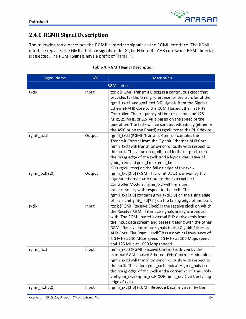
2.4.8 RGMII Signal Description The following table describes the RGMII’s interface signals as the RGMII interface. The RGMII interface replaces the GMII interface signals in the Gigbit Ethernet -‐ AHB core when RGMII Interface is selected. The RGMII Signals have a prefix of “rgmii_”.
Table 4: RGMII Signal Description
Signal Name I/O Description
RGMII Interace txclk Input txclk (RGMII Transmit Clock) is a continuous clock that
provides for the timing reference for the transfer of the rgmii_txctl, and gmii_txd[3:0] signals from the Gigabit Ethernet-‐AHB Core to the RGMII based Ethernet PHY Controller. The frequency of the txclk should be 125 MHz, 25 MHz, or 2.5 MHz based on the speed of the operation. The txclk will be sent out with delay (either in the ASIC or on the Board) as rgmii_txc to the PHY device.
rgmii_txctl Output rgmii_txctl (RGMII Transmit Control) contains the Transmit Control from the Gigabit Ethernet-‐AHB Core. rgmii_txctl will transition synchronously with respect to the txclk. The value on rgmii_txctl indicates gmii_txen the rising edge of the txclk and a logical derivative of gmii_txen and gmii_txer (rgmii_txen XOR rgmii_txer) on the falling edge of the txclk.
rgmii_txd[3:0] Output rgmii_txd[3:0] (RGMII Transmit Data) is driven by the Gigabit Ethernet-‐AHB Core to the External PHY Controller Module. rgmii_txd will transition synchronously with respect to the txclk. The rgmii_txd[3:0] contains gmii_txd[3:0] on the rising edge of txclk and gmii_txd[7:4] on the falling edge of the txclk
rxclk Input rxclk (RGMII Receive Clock) is the receive clock on which the Receive RGMII Interface signals are synchronous with. The RGMII based external PHY derives this from the input data stream and passes it along with the other RGMII Receive Interface signals to the Gigabit Ethernet-‐AHB Core. The “rgmii_rxclk” has a nominal frequency of 2.5 MHz at 10 Mbps speed, 25 MHz at 100 Mbps speed and 125 MHz at 1000 Mbps speed.
rgmii_rxctl Input rgmii_rxctl (RGMII Receive Control) is driven by the external RGMII based Ethernet PHY Controller Module. rgmii_rxctl will transition synchronously with respect to the rxclk. The value rgmii_rxctl indicates gmii_rxdv on the rising edge of the rxclk and a derivative of gmii_rxdv and gmii_rxer (rgmii_rxdv XOR rgmii_rxer) on the falling edge of rxclk.
rgmii_rxd[3:0] Input rgmii_rxd[3:0] (RGMII Receove Data) is driven by the
Datasheet
Copyright © 2015, Arasan Chip Systems Inc. 25
Signal Name I/O Description
RGMII Interace External PHY Controller Module. rgmii_rxd will transition synchronously with respect to the rxclk. The rgmii_rxd[3:0] contains gmii_rxd [3:0] on the rising edge of rxclk and gmii_rxd[7:4] on the falling edge of the rxclk.
MDIO Interface rgmii_mdc Output rgmii_mdc (GMII/MII MDC) is sourced by the GEMAC
Core to the External Ethernet PHY Controller as the timing reference for transfer of information on the gmii_mdi/gmii_mdo signals. rgmii_mdc is an aperiodic signal that has no maximum high or low times. The minimum high and low times for gmii_mdc will be 160 ns each, and the minimum period for rgmii_mdc will be 400 ns, regardless of the nominal period of txclk and rxclk. Note: The rgmii_mdc is derived from the ahb_clk/axi_clk. The frequency of the rgmii_mdc is 1/64th of the ahb_clk/axi_clk frequency.
rgmii_mdi Input rgmii_mdi (GMII/MII MDI) is the data input signal from the External Ethernet PHY Controller. The Read Data is driven by the PHY synchronously with respect to the rgmii_mdc clock during the read cycles.
rgmii_mdo Output rgmii_mdo (GMII/MII MDO) is the data output signal from the GEMAC Core that is used to drive the control information during the Read/Write cycles to the External PHY Controller. The rgmii_mdo signal is driven by the GEMAC Core synchronously with respect to the rgmii_mdc.
rgmii_mdoen_n Output rgmii_mdoen_n (GMII/MII MDO Enable) is the tri-‐state enable signal to drive the rgmii_mdo on to the MDIO pin. This is a low asserted signal.
Datasheet
Copyright © 2015, Arasan Chip Systems Inc. 26
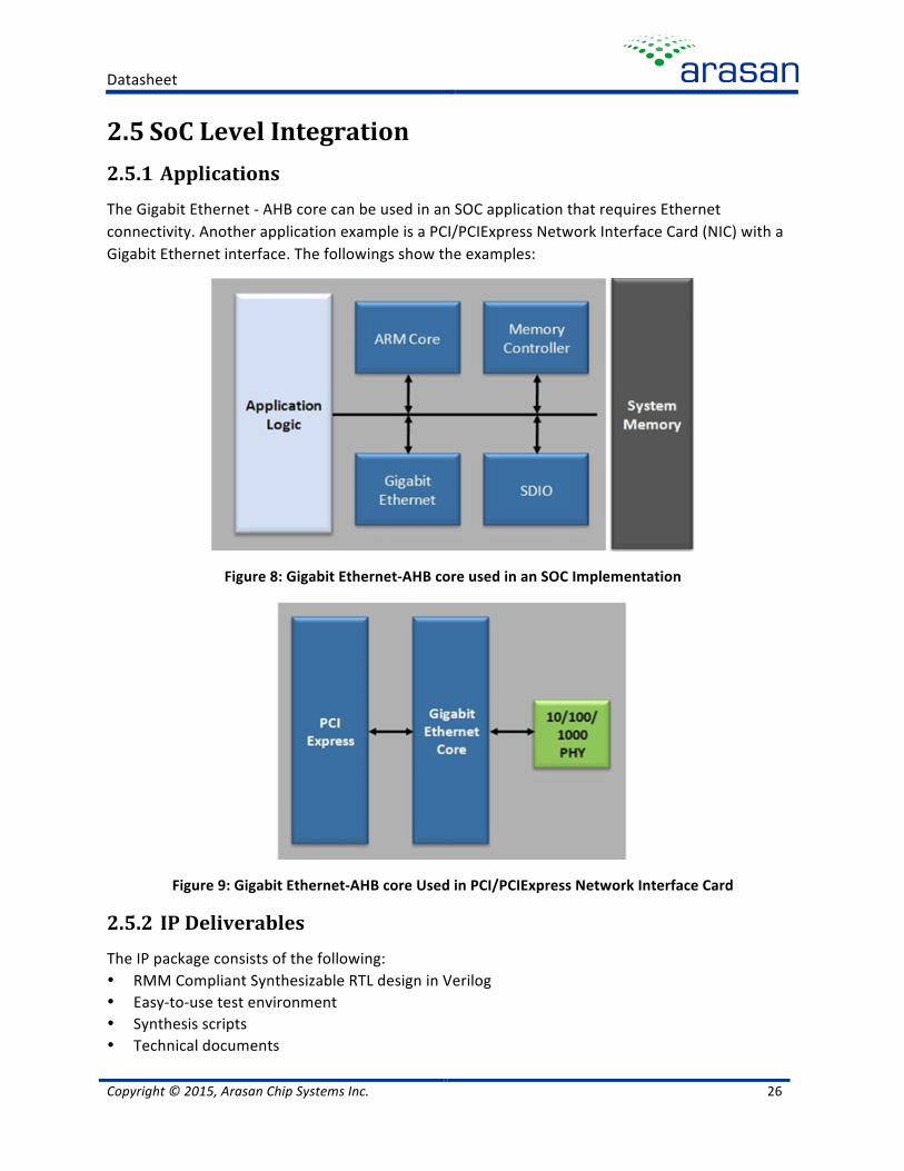
2.5 SoC Level Integration 2.5.1 Applications The Gigabit Ethernet -‐ AHB core can be used in an SOC application that requires Ethernet connectivity. Another application example is a PCI/PCIExpress Network Interface Card (NIC) with a Gigabit Ethernet interface. The followings show the examples:
Figure 8: Gigabit Ethernet-‐AHB core used in an SOC Implementation
Figure 9: Gigabit Ethernet-‐AHB core Used in PCI/PCIExpress Network Interface Card
2.5.2 IP Deliverables The IP package consists of the following: • RMM Compliant Synthesizable RTL design in Verilog • Easy-‐to-‐use test environment • Synthesis scripts • Technical documents

Datasheet
Copyright © 2015, Arasan Chip Systems Inc. 27
3 10 Gigabit Ethernet MAC Controller 3.1 Overview Arasan’s (XGMAC) IP is compliant with the Ethernet IEEE 802.3-‐2008 standard and provides an interface between AHB/AXI Bus and the 10 Gigabit Media Independent Interface (XGMII) using a powerful 64-‐bit Scatter Gather DMA. The 10 Gigabit Ethernet IP is designed for applications such as integrated networking devices, host bus adapters, PCI-‐Express Ethernet controllers, and Ethernet adapter cards.
The XGMAC operates at a speed of 10 Gbps in full duplex mode only. The XGMAC provides features that include transmit and receive message data encapsulation, framing, error code detection, dynamic FCS generation and calculation on frame by frame basis, automatic pad insertion and deletion to enforce minimum frame size requirements. The XGMAC also supports flow control operation by supporting generation and decoding of PAUSE control frames. The XGMAC also supports generation of Management frames on MDC/MDIO signals to communicate with an external PHY device.
The XGMAC IP core consists of two configurable FIFOs on both transmits and receives sides to handle the application’s latency during frame transmission and reception. To enhance the system performance, an AHB/AXI master and a 64-‐bit scatter-‐gather DMA transfer packets between the internal FIFOs and host memory. The XGMAC IP supports the XGMII interface and a MDIO/MDC (Management Data Input/ Output and Management Data Clock) management interface provides control and management functions to external PHY devices. The XGMAC IP also provides enhanced programmable features for minimizing applications complexity and pre/post message processing. The XGMAC IP supports MIB, SNMP, RMON, VLAN Q-‐Tag frame, and Jumbo frames. It also includes dynamic generation, checking, and stripping of FCS field, and automatic pad field insertion. Other features of the XGMAC IP includes generation and decoding of PAUSE control frames, frame boundary delimitation, frame synchronization, and error detection.
3.2 Features • Full-‐duplex mode at 10 Gbps • Supports XGMII interface • Independent 64-‐bit scatter-‐gather DMA with big/ little endian operation • PAUSE frame based flow control in full-‐duplex mode • MDIO/MDC management interface • 802.3 compliant MIB, SNMP, RMON management support • Configurable transmit and receive FIFOs • Supports Jumbo frames • Supports Magic Packet or WakeonLan packets • Optional , PCIe, PCI, or custom bus interfaces

Datasheet
Copyright © 2015, Arasan Chip Systems Inc. 28
3.3 Architecture 3.3.1 Functional Block Diagram The following figure shows the high-‐level block diagram along with various functional blocks of the XGMAC Core.
Figure 10: XGMAC Core Block Diagram
3.3.2 Functional Block Diagram Description
3.3.2.1 XGMII Interface
The XGMAC Core interfaces to the external PHY device using the IEEE802.3 compliant XGMII with 32-‐bit data and 4-‐bit control and independent receive and transmit clocks running at 156.25 MHz.
3.3.2.2 XGMII (64-‐bit data/8-‐bit control) Interface
Optionally provides a 64-‐bit data and 8-‐bit control interface to interface to XG-‐XAUI or XG-‐64B66B PCS Modules. In this mode the XGMAC can run at 156.25 MHz independent transmit/receive clocks or 161.13 MHz independent transmit/receive clocks.

Datasheet
Copyright © 2015, Arasan Chip Systems Inc. 29
3.3.2.3 MDC/MDIO Interface
This is a 2-‐wire interface that is used to configure and control an external IEEE802.3 Compliant PHY device using the MII Management Frame structure. The interface is defined in the IEEE802.3 Specification.
3.3.2.4 AHB/AXI Target (Slave) Interface
The AHB or AXI Target (also called as Slave) Interface provides a 32-‐bit data interface to read/write the internal registers in the XGMAC Core
3.3.2.5 AHB/AXI Master Interface
The AHB Master Interface (64-‐bit or 128-‐bit) is used for bus mastering capability on the AHB Bus by the XGMAC Core. The core generates transactions on this interface to transfer frame data between the Host memory and the internal FIFO’s. Also the Descriptors are transferred using this interface.
3.3.2.6 XGMAC_TX
This module implements the Frame Transmit State Machine by transmitting frames onto XGMII Interface.
3.3.2.7 XGMAC_RX
This module implements the Frame Receive State Machine by receiving frames from XGMII Interface and performing field extraction and error checking.
3.3.2.8 PAUSE_FC
This module decodes the Pause Frames received when the XGMAC Core is in Full Duplex Mode and implements the PAUSE_TIMER to disable the XGMAC_TX module. Also this module generates Pause Frames on Software request.
3.3.2.9 MDC/MDIO Controller
This module generates MDIO Frames (Clause22 or Clause45 Compliant) to talk to external PHY Devices.
3.3.2.10 STATISTICS
This module maintains various counters to perform Statistics for both Transmit and Receive operation.
3.3.2.11 XGMAC_RXFIFO
This module has a configurable FIFO to store the received frames before they are transferred to the Host memory. This module also has additional control logic to flush error packets from the FIFO.

Datasheet
Copyright © 2015, Arasan Chip Systems Inc. 30
3.3.2.12 XGMAC_TXFIFO
This module has a configurable FIFO to store the Frames that are received from the Host memory before the frames are transferred onto Ethernet Interface. This module also has additional FIFO control logic that helps in frame retransmission during Collisions.
3.3.2.13 TXDMA
This module implements the Transmit DMA to transfer the frames from the Host Memory to the Transmit FIFO using the Transmit Descriptors.
3.3.2.14 RXDMA
This module implements the Receive DMA to transfer the frames from the Internal FIFO to the Host Memory using the Receive Descriptors
3.3.2.15 Registers
This module implements the Control and Status Registers to control the operation of Receive and Transmit DMA and also the Receive and Transmit operations of the Ethernet Interface. This module also provides access to the Statistics Counters and provides interrupt/status information to the AHB Host.
3.3.2.16 AHB/AXI Master Interface
This module provides the AHB/AXI Master functionality to generate transactions on the AHB/AXI Bus. The transactions are generated based on the requests from the Transmit/Receive DMA’s.
3.3.2.17 AHB/AXI Target Interface
This module provides the AHB/AXI Target functionality to the AHB/AXI Host (CPU). This interface is used to access all the DMA/MAC registers in the Registers Module.
Datasheet
Copyright © 2015, Arasan Chip Systems Inc. 31
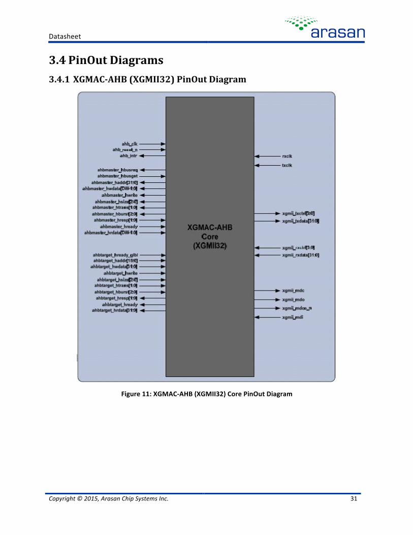
3.4 PinOut Diagrams 3.4.1 XGMAC-‐AHB (XGMII32) PinOut Diagram
Figure 11: XGMAC-‐AHB (XGMII32) Core PinOut Diagram

Datasheet
Copyright © 2015, Arasan Chip Systems Inc. 32
3.4.2 XGMAC-‐AHB (XGMII64) PinOut Diagram
Figure 12: XGMAC-‐AHB (XGMII64) Core PinOut Diagram

Datasheet
Copyright © 2015, Arasan Chip Systems Inc. 33
3.4.3 XGMAC-‐AXI (XGMII32) PinOut Diagram
Figure 13: XGMAC-‐AXI (XGMII32) Core PinOut Diagram

Datasheet
Copyright © 2015, Arasan Chip Systems Inc. 34
3.4.4 XGMAC-‐AXI (XGMII64) PinOut Diagram
Figure 14: XGMAC-‐AXI (XGMII64) Core PinOut Diagram
Datasheet
Copyright © 2015, Arasan Chip Systems Inc. 35
3.4.5 XGMAC Pinout Descriptions The following table describes each of the XGMAC Signal in detail:
• All signals are active high unless specified. Active low signals are suffixed with “_n” • All signals that have prefix of “corecfg_” are Core configuration signals are instantiation time
configuration. • All signals that Interface to the XGMII Interface are prefixed with “xgmii_” • The AHB Clock/Reset/Interrupt signals (when AHB Interface is used) are prefixed with “ahb_” • All signals that Interface to the AHB Master Interface (when AHB Interface is used) are prefixed
with “ahbmaster_” • All signals that Interface to the AHB Target Interface (when AHB Interface is used) are prefixed
with “ahbtarget_” • The AXI Clock/Reset/Interrupt signals (when AHB Interface is used) are prefixed with “axi_” • All signals that Interface to the AXI Master Interface (when AXI Interface is used) are prefixed
with “aximst_” • All signals that Interface to the AXI Slave(Target) Interface (when AXI Interface is used) are
prefixed with “axislv_”
3.5 Signal Interfaces The 10 XGMAC has the following interfaces: • Core Configuration Signals • XGMII Interface Signal Description • AHB Interface Signal Description • AXI Interface Signal Description
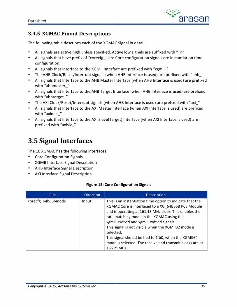
Figure 15: Core Configuration Signals
Pins Direction Description corecfg_64b66bmode Input This is an instantiation time option to indicate that the
XGMAC Core is interfaced to a XG_64B66B PCS Module and is operating at 161.13 MHz clock. This enables the rate matching mode in the XGMAC using the xgmii_rxdtvld and xgmii_txdtvld signals. This signal is not visible when the XGMII32 mode is selected. This signal should be tied to 1’b0, when the XGMII64 mode is selected. The receive and transmit clocks are at 156.25MHz.
Datasheet
Copyright © 2015, Arasan Chip Systems Inc. 36
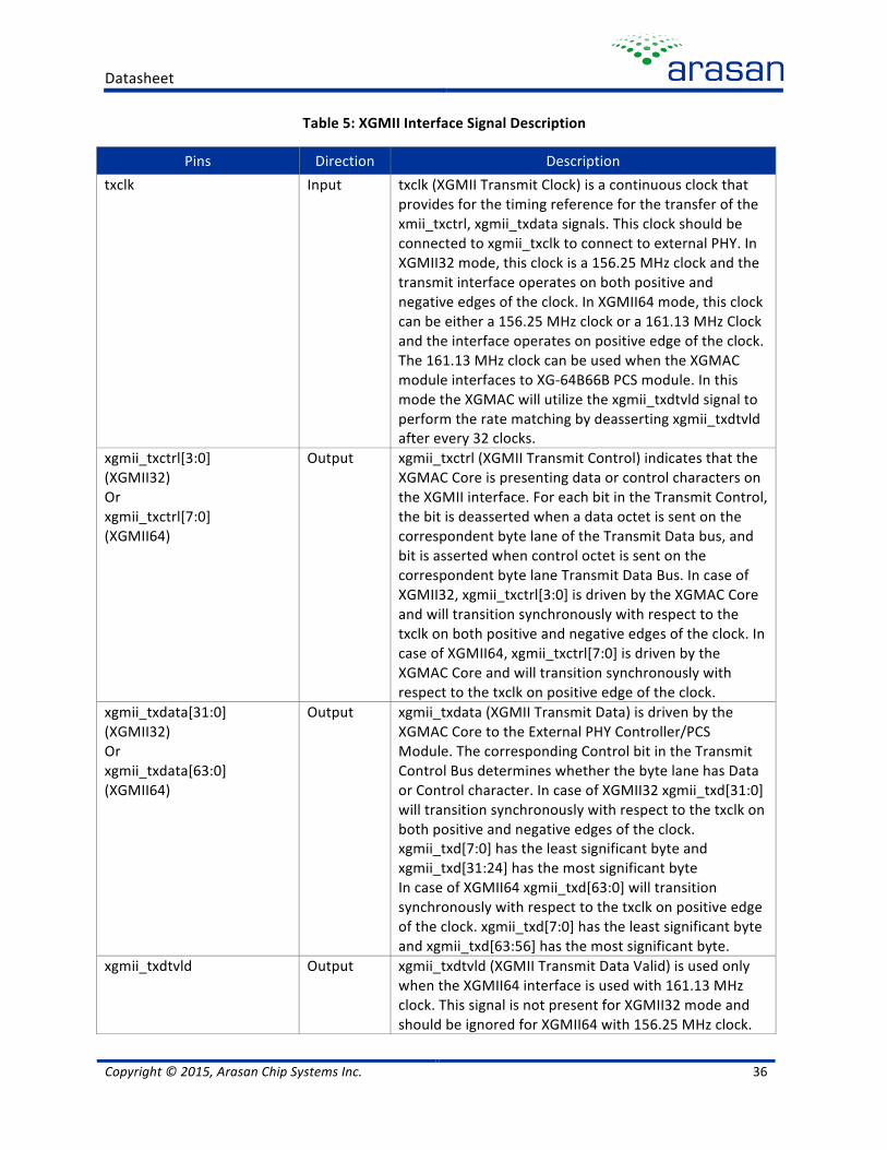
Table 5: XGMII Interface Signal Description
Pins Direction Description txclk Input txclk (XGMII Transmit Clock) is a continuous clock that
provides for the timing reference for the transfer of the xmii_txctrl, xgmii_txdata signals. This clock should be connected to xgmii_txclk to connect to external PHY. In XGMII32 mode, this clock is a 156.25 MHz clock and the transmit interface operates on both positive and negative edges of the clock. In XGMII64 mode, this clock can be either a 156.25 MHz clock or a 161.13 MHz Clock and the interface operates on positive edge of the clock. The 161.13 MHz clock can be used when the XGMAC module interfaces to XG-‐64B66B PCS module. In this mode the XGMAC will utilize the xgmii_txdtvld signal to perform the rate matching by deasserting xgmii_txdtvld after every 32 clocks.
xgmii_txctrl[3:0] (XGMII32) Or xgmii_txctrl[7:0] (XGMII64)
Output xgmii_txctrl (XGMII Transmit Control) indicates that the XGMAC Core is presenting data or control characters on the XGMII interface. For each bit in the Transmit Control, the bit is deasserted when a data octet is sent on the correspondent byte lane of the Transmit Data bus, and bit is asserted when control octet is sent on the correspondent byte lane Transmit Data Bus. In case of XGMII32, xgmii_txctrl[3:0] is driven by the XGMAC Core and will transition synchronously with respect to the txclk on both positive and negative edges of the clock. In case of XGMII64, xgmii_txctrl[7:0] is driven by the XGMAC Core and will transition synchronously with respect to the txclk on positive edge of the clock.
xgmii_txdata[31:0] (XGMII32) Or xgmii_txdata[63:0] (XGMII64)
Output xgmii_txdata (XGMII Transmit Data) is driven by the XGMAC Core to the External PHY Controller/PCS Module. The corresponding Control bit in the Transmit Control Bus determines whether the byte lane has Data or Control character. In case of XGMII32 xgmii_txd[31:0] will transition synchronously with respect to the txclk on both positive and negative edges of the clock. xgmii_txd[7:0] has the least significant byte and xgmii_txd[31:24] has the most significant byte In case of XGMII64 xgmii_txd[63:0] will transition synchronously with respect to the txclk on positive edge of the clock. xgmii_txd[7:0] has the least significant byte and xgmii_txd[63:56] has the most significant byte.
xgmii_txdtvld Output xgmii_txdtvld (XGMII Transmit Data Valid) is used only when the XGMII64 interface is used with 161.13 MHz clock. This signal is not present for XGMII32 mode and should be ignored for XGMII64 with 156.25 MHz clock.
Datasheet
Copyright © 2015, Arasan Chip Systems Inc. 37
Pins Direction Description This signal is used to do rate matching with the XG_64B66B PCS Module. This signal is deasserted after every 32 clocks on continuous basis. xgmii_txdtvld is driven by the XGMAC Core and will transition synchronously with respect to the txclk. When asserted the xgmii_txdtvld will be at logic '1' and it will be at logic '0' while deasserted.
rxclk Input rxclk (XGMII Receive Clock) is the receive clock on which the Receive XGMII Interface signals are synchronous with. The XGMII based external PHY derives this from the input data stream and passes it along with the other XGMII Receive Interface signals to the XGMAC Core. In XGMII32 mode, this clock has a nominal frequency of 156.25 MHz clock and the receive interface operates on both positive and negative edges of the clock. In XGMII64 mode, this clock can be either a nominal 156.25 MHz clock or a nominal 161.13 MHz Clock and the receive interface operates on positive edge of the clock. The 161.13 MHz clock can be used when the XGMAC module interfaces to XG-‐64B66B PCS module. In this mode the XGMAC utilizes the xgmii_rxdtvld signal to determine whether the xgmii_rxdata and xgmii_rxctrl signals are valid
xgmii_rxctrl[3:0] (XGMII32) Or xgmii_rxctrl[7:0] (XGMII64)
Input xgmii_rxctrl (XGMII Receive Control) indicates that the PHY is presenting data or control characters on the XGMII interface. For each bit in the Receive Control, the bit is deasserted when a data octet is sent on the correspondent byte lane of the Receive Data bus, and bit is asserted when control octet is sent on the correspondent byte lane Receive Data Bus. In case of XGMII32, xgmii_rxctrl[3:0] is driven by the PHY and will transition synchronously withrespect to the rxclk on both positive and negative edges of the clock. In case of XGMII64, xgmii_rxctrl[7:0] is driven by the PHY/PCS Module and will transition synchronously with respect to the rxclk on positive edge of the clock.
xgmii_rxdata[31:0] (XGMII32) Or xgmii_rxdata[63:0] (XGMII64)
Input xgmii_rxdata (XGMII Receive Data) is driven by the External PHY Controller/PCS Module. The corresponding Control bit in the Receive Control Bus determines whether the byte lane has Data or Control character. In case of XGMII32 xgmii_rxd[31:0] will transition synchronously with respect to the rxclk on both positive and negative edges
Datasheet
Copyright © 2015, Arasan Chip Systems Inc. 38
Pins Direction Description of the clock xgmii_rxd[7:0] has the least significant byte and xgmii_rxd[31:24] has the most significant byte In case of XGMII64 xgmii_rxd[63:0] will transition synchronously with respect to the rxclk on positive edge of the clock xgmii_rxd[7:0] has the least significant byte and xgmii_rxd[63:56] has the most significant byte
xgmii_rxdtvld Input xgmii_rxdtvld (XGMII Receive Data Valid) is used only when the XGMII64 interface is used with 161.13 MHz clock. This signal is not present for XGMII32 mode and should be tied to 1’b1 for XGMII64 mode with 156.25 MHz clock. This signal is used to do rate matching by the XG_64B66B PCS Module. This signal is expected to be deasserted after every 32 clocks on continuous basis. xgmii_txdtvld is driven by the XG_64B66B PCS Module and will transition synchronously with respect to the txclk. When asserted the xgmii_txdtvld will be at logic '1' and it will be at logic '0' while de-‐asserted.
MDIO Interface xgmii_mdc Output xgmii_mdc (XGMII MDC) is sourced by the XGMAC Core
to the External Ethernet PHY Controller as the timing reference for transfer of information on the xgmii_mdi/xgmii_mdo signals. xgmii_mdc is an a periodic signal that has no maximum high or low times. The minimum high and low times for gmii_mdc will be 160 ns each, and the minimum period for xgmii_mdc will be 400 ns, regardless of the nominal period of txclk and rxclk. Note: The xgmii_mdc is derived from the ahb_clk/axi_clk. The frequency of the xgmii_mdc is 1/64th of the ahb_clk/axi_clk frequency.
xgmii_mdi Input xgmii_mdi (XGMII MDI) is the data input signal from the External Ethernet PHY Controller. The Read Data is driven by the PHY synchronously with respect to the xgmii_mdc clock during the read cycles.
xgmii_mdo Output xgmii_mdo (XGMII MDO) is the data output signal from the XGMAC Core that is used to drive the control information during the Read/Write cycles to the External PHY Controller. The xgmii_mdo signal is driven by the XGMAC Core synchronously with respect to the xgmii_mdc.
xgmii_mdoen_n Output xgmii_mdoen_n (XGMII MDO Enable) is the tri-‐state enable signal to drive the xgmii_mdo on to the MDIO pin. This is a low asserted signal.

Datasheet
Copyright © 2015, Arasan Chip Systems Inc. 39
Table 6: AHB Interface Signal Description
Pins Direction Description
AHB Clock/Reset/Interrupt Signals ahb_clk Input ahb_clk (AHB Clock) is the system clock on which both
the AHB Master Interface and AHB Target Interface is synchronous to
ahb_reset_n Input ahb_reset_n (AHB Reset) is the System Reset to reset the XGMAC Core to the default State. This is an active low signal. When asserted, this signal must be asserted for at least 64 Clock cycles
ahb_intr Output Interrupt Output to the AHB Bus
AHB Master Interface Signals ahbmaster_hbusreq Output Bus Request on the AHB Master Interface
ahbmaster_hgrant Input Bus Grant on the AHB Master Interface
ahbmaster_haddr [31:0]
Output Bus Address on the AHB Master Interface. This is a Byte Addressable Address
ahbmaster_hwdata [(DW-‐1):0]
Output Write Data on the AHB Master Interface. The Width of the bus is based on the Selected Host Data Bus Width. Here DW is 64 for 64-‐bit bus, and DW is 128 for 128-‐bit bus
ahbmaster_hrdata [(DW-‐1):0]
Input Read Data on the AHB Master Interface. The Width of the bus is based on the Selected Host Data Bus Width. Here DW is 64 for 64-‐bit bus, and DW is 128 for 128-‐bit bus.
ahbmaster_hwrite Output Write or Read Direction Indication for the current AHB Master transaction. 1’b1: Write 1’b0: Read
ahbmaster_hsize [2:0]
Output Size of the Data width. The AHB Master interface supports 8, 16, 32, 64 and 128-‐bit data transfers. The 128-‐bit data transfers are valid only when the Host data Bus Width is 128-‐bits. The following are the valid size values that are output by the XGMAC Core. 000: 8-‐bit Data Transfer Size 001: 16-‐bit Data Transfer Size 010: 32-‐bit Data Transfer Size 011: 64-‐bit Data Transfer Size 100: 128-‐bit Data Transfer Size
ahbmaster_htrans [1:0]
Output Transfer Type
ahbmaster_hbusreq Output Bus Request on the AHB Master Interface
ahbmaster_hgrant Input Bus Grant on the AHB Master Interface
ahbmaster_haddr [31:0]
Output Bus Address on the AHB Master Interface. This is a Byte Addressable Address

Datasheet
Copyright © 2015, Arasan Chip Systems Inc. 40
Pins Direction Description
AHB Target Interface Signals ahbtarget_haddr [15:0] Input Bus Address on the AHB Target Interface. This is a Byte
Addressable Address Only 16-‐bits of the Address are used All Registers in the XGMAC Core are 32-‐bit aligned
ahbtarget_hwdata [31:0]
Input Write Data on the AHB Target Interface
ahbtarget_hrdata [31:0]
Output Read Data on the AHB Target Interface
ahbtarget_hwrite Input Write or Read Direction Indication for the current AHB Target transaction 1’b1: Write 1’b0: Read
ahbtarget_hsize [2:0]
Input Size of the Data width. The AHB Target Interface supports only 32-‐bit data transfers. Thus the Size should be fixed to 3’b010 for all data transfers.
ahbtarget_htrans [1:0]
Input Transfer Type
ahbtarget_hburst [2:0]
Input Burst Size for the current AHB Target transaction. The Target Interface supports only SINGLE transaction and no burst support.
ahbtarget_hready Output Target Ready from XGMAC
ahbtarget_hresp [1:0]
Output Transfer Response for the Current AHB Target transaction
ahbtarget_hready_glbl Input Selected HReady from all Targets. This is the signal that feeds to AHB Targets
Table 7: AXI Interface Signal Description
Pins Direction Description
AXI Clock/Reset/Interrupt Signals axi_clk Input axi_clk (AXI Clock) is the system clock on which both the
AXI Master Interface and AXI Slave(Target) Interface is synchronous to
axi_reset_n Input axi_reset_n (AXI Reset) is the System Reset to reset the XGMAC Core to the default State. This is an active low signal. When asserted, this signal must be asserted for at least 64 Clock cycles.
axi_intr Output Interrupt Output to the AXI Bus
AXI Master Write Interface Signals aximst_awid [3:0]
Output Write address ID. This signal is the identification tag for the write address group of signals.
aximst_awaddr Output Write address. The write address bus gives the address
Datasheet
Copyright © 2015, Arasan Chip Systems Inc. 41
Pins Direction Description [31:0] of the first transfer in a write burst transaction. The
associated control signals are used to determine the addresses of the remaining transfers in the burst
aximst_awlen [3:0]
Output Burst length. The burst length gives the exact number of transfers in a burst. This information determines the number of data transfers associated with the address. Refer to AMBA Specification for encoding of this field.
aximst_awsize [2:0]
Output Burst size. This signal indicates the size of each transfer in the burst. Byte lane strobes indicate exactly which byte lanes to update. The AXI Master interface supports 8, 16, 32, 64 and 128-‐bit wide data transfers. The 128-‐bit data transfer size is supported only when the Host Data Bus Width is 128-‐bits. The following are the valid size values that are output by the XGMAC Core. 000: 8-‐bit Data Transfer Size 001: 16-‐bit Data Transfer Size 010: 32-‐bit Data Transfer Size 011: 64-‐bit Data Transfer Size 100: 128-‐bit Data Transfer Size
aximst_awburst [1:0]
Output Burst type. The burst type, coupled with the size information, details how the address for each transfer within the burst is calculated. The AXI Master interface always uses INCR Burst with value of 2’b00.
aximst_awvalid Output Write address valid. This signal indicates that valid write address and control information are available: 1 = address and control information available 0 = address and control information not available. The address and control information remain stable until the address acknowledge signal, aximst_awready (AWREADY), goes HIGH.
aximst_awready Input Write address ready. This signal indicates that the slave is ready to accept an address and associated control signals: 1 = slave ready 0 = slave not ready
aximst_wid [3:0]
Output Write ID tag. This signal is the ID tag of the write data transfer. The aximst_wid (WID) value matches the aximst_awid (AWID) value of the write transaction
aximst_wdata [(DW-‐1):0]
Output Write data. The write data bus is either 64-‐bits (DW= 64) or 128 (DW=128) based on the selected Host Data Bus Width.
aximst_wstrb [(BW-‐1):0]
Output Write strobes. This signal indicates which byte lanes to are valid in the aximst_wdata bus. There is one write strobe for each eight bits of the write data bus. The
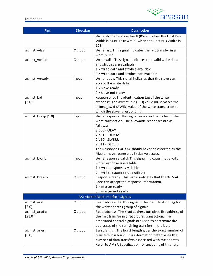
Datasheet
Copyright © 2015, Arasan Chip Systems Inc. 42
Pins Direction Description Write strobe bus is either 8 (BW=8) when the Host Bus Width is 64 or 16 (BW=16) when the Host Bus Width is 128.
aximst_wlast Output Write last. This signal indicates the last transfer in a write burst
aximst_wvalid Output Write valid. This signal indicates that valid write data and strobes are available: 1 = write data and strobes available 0 = write data and strobes not available
aximst_wready Input Write ready. This signal indicates that the slave can accept the write data: 1 = slave ready 0 = slave not ready
aximst_bid [3:0]
Input Response ID. The identification tag of the write response. The aximst_bid (BID) value must match the aximst_awid (AWID) value of the write transaction to which the slave is responding
aximst_bresp [1:0] Input Write response. This signal indicates the status of the write transaction. The allowable responses are as follows: 2’b00 -‐ OKAY 2’b01 -‐ EXOKAY 2’b10 -‐ SLVERR 2’b11 -‐ DECERR. The Response EXOKAY should never be asserted as the Master never generates Exclusive access.
aximst_bvalid Input Write response valid. This signal indicates that a valid write response is available: 1 = write response available 0 = write response not available
aximst_bready Output Response ready. This signal indicates that the XGMAC Core can accept the response information. 1 = master ready 0 = master not ready
AXI Master Read Interface Signals aximst_arid [3:0]
Output Read address ID. This signal is the identification tag for the write address group of signals.
aximst_araddr [31:0]
Output Read address. The read address bus gives the address of the first transfer in a read burst transaction. The associated control signals are used to determine the addresses of the remaining transfers in the burst.
aximst_arlen [3:0]
Output Burst length. The burst length gives the exact number of transfers in a burst. This information determines the number of data transfers associated with the address. Refer to AMBA Specification for encoding of this field.

Datasheet
Copyright © 2015, Arasan Chip Systems Inc. 43
Pins Direction Description aximst_arsize [2:0]
Output Burst size. This signal indicates the size of each transfer in the burst. Byte lane strobes indicate exactly which byte lanes to update. The AXI Master interface supports 8, 16, 32, 64 and 128-‐bit wide data transfers. The 128-‐bit data transfer size is supported only when the Host Data Bus Width is 128-‐bits. The following are the valid size values that are output by the XGMAC Core. 000: 8-‐bit Data Transfer Size 001: 16-‐bit Data Transfer Size 010: 32-‐bit Data Transfer Size 011: 64-‐bit Data Transfer Size 100: 128-‐bit Data Transfer Size
aximst_arburst [1:0]
Output Burst type. The burst type, coupled with the size information, details how the address for each transfer within the burst is calculated. The AXI Master interface always uses INCR Burst with value of 2’b00.
aximst_arvalid Output Read address valid. This signal indicates that valid read address and control information are available: 1 = address and control information available 0 = address and control information not available. The address and control information remain stable until the address acknowledge signal, aximst_arready (ARREADY), goes HIGH.
aximst_arready Input Read address ready. This signal indicates that the slave is ready to accept an address and associated control signals: 1 = slave ready 0 = slave not ready.
aximst_rid [3:0] Input Read ID tag. This signal is the ID tag of the read data transfer. The aximst_rid (RID) value matches the aximst_arid (ARID) value of the read transaction
aximst_rdata [(DW-‐1):0]
Input Read data. The read data bus is either 64-‐bits (DW=64) or 128 (DW=128) based on the selected Host Data Bus Width.
aximst_rresp [1:0]
Input Read response. This signal indicates the status of the read transaction. The allowable responses are as follows: 2’b00 -‐ OKAY 2’b01 -‐ EXOKAY 2’b10 -‐ SLVERR 2’b11 -‐ DECERR. The Response EXOKAY should never be asserted as the Master never generates Exclusive access
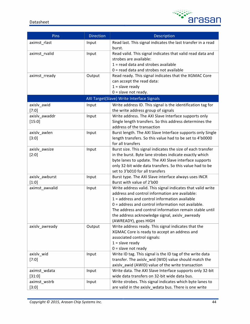
Datasheet
Copyright © 2015, Arasan Chip Systems Inc. 44
Pins Direction Description aximst_rlast Input Read last. This signal indicates the last transfer in a read
burst. aximst_rvalid Input Read valid. This signal indicates that valid read data and
strobes are available: 1 = read data and strobes available 0 = read data and strobes not available
aximst_rready Output Read ready. This signal indicates that the XGMAC Core can accept the read data: 1 = slave ready 0 = slave not ready.
AXI Target(Slave) Write Interface Signals axislv_awid [7:0]
Input Write address ID. This signal is the identification tag for the write address group of signals
axislv_awaddr [15:0]
Input Write address. The AXI Slave Interface supports only Single length transfers. So this address determines the address of the transaction
axislv_awlen [3:0]
Input Burst length. The AXI Slave Interface supports only Single length transfers. So this value had to be set to 4’b0000 for all transfers
axislv_awsize [2:0]
Input Burst size. This signal indicates the size of each transfer in the burst. Byte lane strobes indicate exactly which byte lanes to update. The AXI Slave interface supports only 32-‐bit wide data transfers. So this value had to be set to 3’b010 for all transfers
axislv_awburst [1:0]
Input Burst type. The AXI Slave interface always uses INCR Burst with value of 2’b00
aximst_awvalid Input Write address valid. This signal indicates that valid write address and control information are available: 1 = address and control information available 0 = address and control information not available. The address and control information remain stable until the address acknowledge signal, axislv_awready (AWREADY), goes HIGH
axislv_awready Output Write address ready. This signal indicates that the XGMAC Core is ready to accept an address and associated control signals: 1 = slave ready 0 = slave not ready
axislv_wid [7:0]
Input Write ID tag. This signal is the ID tag of the write data transfer. The axislv_wid (WID) value should match the axislv_awid (AWID) value of the write transaction
aximst_wdata [31:0]
Input Write data. The AXI Slave Interface supports only 32-‐bit wide data transfers on 32-‐bit wide data bus.
aximst_wstrb [3:0]
Input Write strobes. This signal indicates which byte lanes to are valid in the axislv_wdata bus. There is one write

Datasheet
Copyright © 2015, Arasan Chip Systems Inc. 45
Pins Direction Description strobe for each eight bits of the write data bus.
axislv_wlast Input Write last. This signal indicates the last/only transfer in a write burst
axislv_wvalid Input Write valid. This signal indicates that valid write data and strobes are available: 1 = write data and strobes available 0 = write data and strobes not available
axislv_wready Output Write ready. This signal indicates that the XGMAC Core can accept the write data: 1 = slave ready 0 = slave not ready
axislv_bid [7:0]
Output Response ID. The identification tag of the write response. The axislv_bid (BID) value matches the axislv_awid (AWID) value of the write transaction to which the slave is responding
axislv_bresp [1:0]
Output Write response. This signal indicates the status of the write transaction. The allowable responses are as follows: 2’b00 -‐ OKAY 2’b01 -‐ EXOKAY 2’b10 -‐ SLVERR 2’b11 -‐ DECERR. The Response EXOKAY will never be asserted as the Slave does not support Exclusive access
axislv_bvalid Output Write response valid. This signal indicates that a valid write response is available: 1 = write response available 0 = write response not available
axislv_bready Input Response ready. This signal indicates that the master can accept the response information 1 = master ready 0 = master not ready
AXI Slave Read Interface Signals axislv_arid [7:0] Input Read address ID. This signal is the identification tag for
the write address group of signals axislv_araddr [15:0]
Input Read address. The AXI Slave Interface supports only Single length transfers. So this address determines the address of the transaction.
axislv_arlen [3:0]
Input Burst length. The AXI Slave Interface supports only Single length transfers. So this value had to be set to 4’b0000 for all transfers.
axislv_arsize [2:0]
Input Burst size. This signal indicates the size of each transfer in the burst. Byte lane strobes indicate exactly which byte lanes to update. The AXI Slave interface supports only 32-‐bit wide data transfers. So this value had to be

Datasheet
Copyright © 2015, Arasan Chip Systems Inc. 46
Pins Direction Description set to 3’b010 for all transfers.
axislv_arburst [1:0]
Input Burst type. The AXI Slave interface always uses INCR Burst with value of 2’b00.
axislv_arvalid Input Read address valid. This signal indicates that valid write address and control information are available: 1 = address and control information available 0 = address and control information not available. The address and control information remain stable until the address acknowledge signal, axislv_arready (ARREADY), goes HIGH.
axislv_arready Output Write address ready. This signal indicates that the XGMAC Core is ready to accept an address and associated control signals: 1 = slave ready 0 = slave not ready.
axislv_rid [7:0]
Output Read ID tag. This signal is the ID tag of the read data transfer. The axislv_rid (RID) value matches the axislv_arid (ARID) value of the read transaction
aximst_rdata [31:0]
Output Read data. The AXI Slave Interface supports only 32-‐bit wide data transfers on 32-‐bit wide data bus.
axislv_rresp [1:0]
Output Read response. This signal indicates the status of the read transaction. The allowable responses are as follows: 2’b00 -‐ OKAY 2’b01 -‐ EXOKAY 2’b10 -‐ SLVERR 2’b11 – DECERR The Response EXOKAY should never be asserted as the Master never generates Exclusive access
axislv_rlast Output Read last. This signal indicates the last transfer in a read burst
axislv_rvalid Output Read valid. This signal indicates that valid read data and strobes are available: 1 = read data and strobes available 0 = read data and strobes not available
axislv_rready Input Read ready. This signal indicates that the Master can accept the read data: 1 = slave ready 0 = slave not ready

Datasheet
Copyright © 2015, Arasan Chip Systems Inc. 47
3.6 SoC Level Integration 3.6.1 XGMAC Applications The XGMAC Core can be used in a PCI/PCIExpress based NIC Controller or an Aggregation/Switch device with 10G Host Interface. The following are two simple applications of the XGMAC Core:
• XGMAC Core in a SOC Application • XGMAC Core in an NIC Application
Figure 16: XGMAC Core used in PCIExpress based NIC Controller
Figure 17: XGMAC Core used Aggregation/Switch Device

Datasheet
Copyright © 2015, Arasan Chip Systems Inc. 48
3.6.2 IP Deliverables The IP package consists of the following:
• RMM Compliant Synthesizable RTL design in Verilog • Easy-‐to-‐use test environment • Synthesis scripts • Technical documents
Datasheet
Copyright © 2015, Arasan Chip Systems Inc. 49
4 Gigabit Ethernet with IEEE 1588 MAC Controller
4.1 Introduction The Gigabit Ethernet Media Access Controller (GEMAC) with AHB or AXI Interface (GEMAC) core incorporates the essential protocol requirements for operation of 10/100/1000 Mbps Ethernet/IEEE 802.3-‐2008 compliant node, and provides interface between the AHB or AXI Interface and the Media Independent Interface (MII) for 10/100 Mbps speeds and Gigabit Media Independent Interface (GMII) for 1000 Mbps Speed with hardware assisted support for IEEE-‐1588 protocol. Optionally the core supports SGMII (Serial GMII Interface) and GMII (Reduced GMII) Interface for reducing the pin count to interface with external PHY device.
The GEMAC core can operate at 10 Mbps or 100 Mbps (Fast Ethernet) or 1000 Mbps (Gigabit Ethernet). On the System side the GEMAC Core implements 32-‐bit or 64-‐bit AHB/AXI Master Interface logic and 32-‐bit AHB/AXI Target (Slave) Interface logic to interface with AHB/AXI Bus and a powerful 32-‐bit or 64-‐bit Scatter-‐Gather DMA to transfer packets between HOST Memory and Internal FIFO’s. The GEMAC Core supports configurable FIFO’s on both transmit and receive side to handle the Application’s latency during the frame transmission and reception.
The GEMAC Core supports Half-‐Duplex mode of operation for 10/100 Mbps speeds and Full-‐Duplex mode of operation for 10/100/1000 Mbps speeds. When operating in the half-‐duplex mode, the GEMAC Core is fully compliant to Section 4 of ISO/IEC 8802-‐3 (ANSI/IEEE Standard) and ANSI/IEEE 802.3. When operating in the full duplex mode, the GEMAC core is compliant to the IEEE 802.3x standard for full-‐duplex operation.
4.2 Overview The Arasan Gigabit Ethernet Media Access Controller IP is compliant with the Ethernet IEEE 802.3-‐2008 standard. The Gigabit Ethernet IP provides a 10/100 Mbps Media Independent Interface (MII) and a 1000 Mbps Gigabit Media Independent Interface (GMII). It also supports optional Reduced MII (RGMII), and Serial GMII (SGMII). The Gigabit Ethernet IP also implements Hardware assisted 1588 Protocol for Time stamping the Receive and Transmit PTP Packets.
The Gigabit Ethernet IP is designed for SoC and mobile applications such as integrated networking devices, PCI-‐Express Ethernet controllers, and Ethernet adapter cards. The Gigabit Ethernet IP supports half-‐duplex mode at 10/100 Mbps and full-‐duplex mode at 10/100/1000 Mbps. The Gigabit Ethernet IP core consists of two configurable FIFOs on both transmits and receives sides to handle the application’s latency during frame transmission and reception. A processor bus master and a 32-‐bit scatter-‐gather DMA transfer packets between the internal FIFOs and the host memory to enhance system performance. The Gigabit Ethernet IP supports 4-‐bit MII based 10/100 Mbps PHY and 8-‐bit GMII based 10/100/1000 Mbps PHY. A MDIO/MDC (Management Data Input/Output

Datasheet
Copyright © 2015, Arasan Chip Systems Inc. 50
and Management Data Clock) management interface provides control and management functions to external PHY devices.
The Gigabit Ethernet IP also provides enhanced programmable features for minimizing applications complexity and pre/post message processing. The Gigabit Ethernet IP supports MIB, SNMP, RMON, VLAN Q-‐Tag frame, and Jumbo frames. It also includes dynamic generation, checking, and stripping of FCS field, automatic pad field insertion, automatic retransmission and detection of collision frames, collision avoidance and handling. Other features of the Gigabit Ethernet IP includes generation and decoding of PAUSE control frames, frame boundary delimitation, frame synchronization, and error detection.
The GEMAC Core provides programmable enhanced features designed to minimize Applications complexity and pre/post message processing. These features include dynamic FCS generation on a frame-‐by-‐frame basis, automatic pad field insertion to enforce minimum frame size requirement, automatic retransmission and detection of collision frames (in Half Duplex mode), FCS checking on incoming frames, optional stripping of FCS field, automatic detection of PAUSE Control frames when operating in Full-‐Duplex mode, performing Address Filtering on receive frames and so on.
The GEMAC Core provides hardware assisted IEEE-‐1588 (both V1 and V2) Protocol Support when operating in Full-‐Duplex modes at 10/100/1000 Mbps speeds of operation. The GEMAC Core maintains a system timer and provides software interface for adjusting the system timer. Also provides support for time stamping of receive and transmit Packets.
The DMA Controller in the GEMAC Core is a powerful scatter-‐gather based direct memory access (DMA) with programmable Burst size, providing Low CPU utilization. The DMA can operate either in 32-‐bit data transfer mode or 64-‐bit data transfer mode. The transfer size on the AHB/AXI bus is sized accordingly. The DMA transfers frames to/from the internal FIFO’s and the data buffers in the Host Memory. Descriptors that reside in the Host memory act as pointers to these buffers. The DMA supports Transmit and Receive operations independently. The DMA is controlled by a set of Registers called DMA Registers.
The GEMAC core can sustain transmission of minimal-‐sized back-‐to-‐back packets at full line speed with an inter-‐packet gap (IPG) of 96 bit-‐times equivalent to 90.6 us for 10-‐Mb/s, 0.96 us for 100-‐Mb/s, and 0.096 us for 1000-‐Mbps speed. On receive side the GEMAC core can handle reception of minimal-‐sized back to back frames at full line speed with IPG of 64 bit times.
4.3 Features • Hardware Assisted 1588 V1/V2 Support • Full-‐duplex mode at 10/100/1000 Mbps • Half-‐duplex mode at 10/100 Mbps • Supports IEEE 802.3-‐2008 compliant MII, RMII, SMII, GMII, RGMII, and SGMII • Independent 32-‐bit scatter-‐gather DMA with big/ little endian operation • Optional VLAN Q-‐Tag frame support • CSMA/CD Protocol for half-‐duplex mode
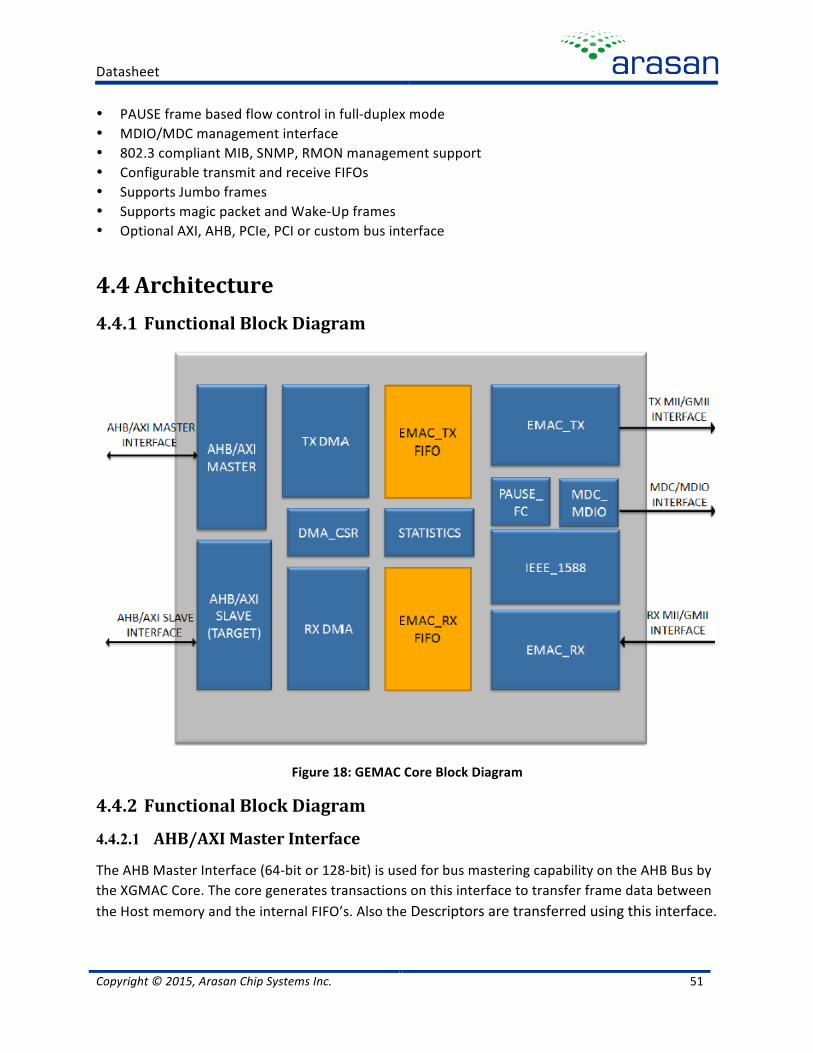
Datasheet
Copyright © 2015, Arasan Chip Systems Inc. 51
• PAUSE frame based flow control in full-‐duplex mode • MDIO/MDC management interface • 802.3 compliant MIB, SNMP, RMON management support • Configurable transmit and receive FIFOs • Supports Jumbo frames • Supports magic packet and Wake-‐Up frames • Optional AXI, AHB, PCIe, PCI or custom bus interface
4.4 Architecture 4.4.1 Functional Block Diagram
Figure 18: GEMAC Core Block Diagram
4.4.2 Functional Block Diagram
4.4.2.1 AHB/AXI Master Interface
The AHB Master Interface (64-‐bit or 128-‐bit) is used for bus mastering capability on the AHB Bus by the XGMAC Core. The core generates transactions on this interface to transfer frame data between the Host memory and the internal FIFO’s. Also the Descriptors are transferred using this interface.

Datasheet
Copyright © 2015, Arasan Chip Systems Inc. 52
4.4.2.2 AHB/AXI Slave (Target) Interface
The AHB or AXI Target (also called as Slave) Interface provides a 32-‐bit data interface to read/write the internal registers in the GEMAC Core.
4.4.2.3 GMII/MII Interface
The GEMAC Core interfaces to the external PHY device using the IEEE802.3 compliant GMII/MII Interface. In case of 10/100 Mbps, the MII Interface (4-‐bit wide) is used and when operating in 1000 Mbps mode, the GMII Interface (8-‐bit wide) is used. This interface is specified in the IEEE 802.3 specification. Any of the Standard Ethernet PHY Controller Chips can be hooked onto this interface for connecting to the Ethernet Cable.
4.4.2.4 MDC/MDIO Interface
This is a 2-‐wire interface that is used to configure and control an external IEEE802.3 Compliant PHY device using the MII Management Frame structure. The interface is defined in the IEEE802.3 Specification.
4.4.2.5 SGMII/RGMII Interface
The GEMAC Core optionally supports Reduced GMII (RGMII) and Serial GMII (SGMII) Interfaces to reduce the pin count on the Ethernet Interface.
4.4.2.6 AHB/AXI Master Interface Module
This module provides the AHB/AXI Master functionality to generate transactions on the AHB/AXI Bus. The transactions are generated based on the requests from the Transmit/Receive DMA’s
4.4.2.7 AHB/AXI Target Interface Module
This module provides the AHB/AXI Target functionality to the AHB/AXI Host (CPU). This interface is used to access all the DMA/MAC registers in the Registers Module
4.4.2.8 TXDMA
This module implements the Transmit DMA to transfer the frames from the Host Memory to the Transmit FIFO using the Transmit Descriptors
4.4.2.9 Registers
This module implements the Control and Status Registers to control the operation of Receive and Transmit DMA and also the Receive and Transmit operations of the Ethernet Interface. This module also provides access to the Statistics Counters and provides interrupt/status information to the AHB Host
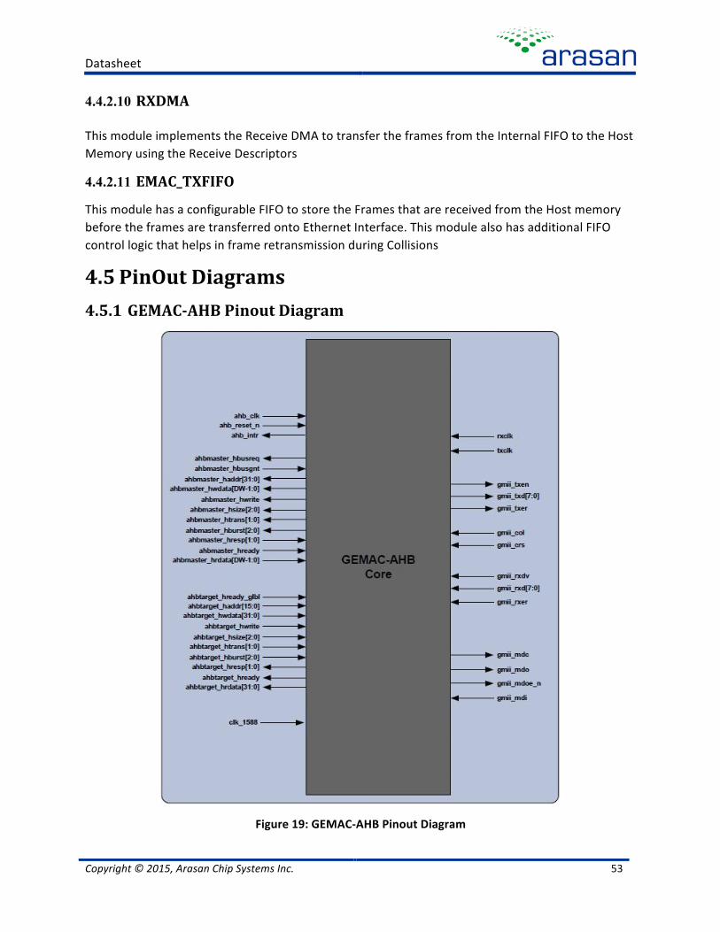
Datasheet
Copyright © 2015, Arasan Chip Systems Inc. 53
4.4.2.10 RXDMA This module implements the Receive DMA to transfer the frames from the Internal FIFO to the Host Memory using the Receive Descriptors
4.4.2.11 EMAC_TXFIFO
This module has a configurable FIFO to store the Frames that are received from the Host memory before the frames are transferred onto Ethernet Interface. This module also has additional FIFO control logic that helps in frame retransmission during Collisions
4.5 PinOut Diagrams 4.5.1 GEMAC-‐AHB Pinout Diagram
Figure 19: GEMAC-‐AHB Pinout Diagram

Datasheet
Copyright © 2015, Arasan Chip Systems Inc. 54
4.5.2 GEMAC-‐AXI Core Pin-‐ Out Diagram
Figure 20: GEMAC-‐ AXI Core Pin-‐ Out Diagram
Datasheet
Copyright © 2015, Arasan Chip Systems Inc. 55
4.5.3 Pinout Descriptions The following table describes each of the GEMAC Signal in detail. All signals are active high unless specified.
• Active low signals are suffixed with “_n” • All signals that Interface to the MII/GMII Interface are prefixed with “gmii_” • The AHB Clock/Reset/Interrupt signals (when AHB Interface is used) are prefixed with “ahb_” • All signals that Interface to the AHB Master Interface (when AHB Interface is used) are prefixed
with “ahbmaster_” • All signals that Interface to the AHB Target Interface (when AHB Interface is used) are prefixed
with “ahbtarget_” • The AXI Clock/Reset/Interrupt signals (when AHB Interface is used) are prefixed with “axi_” • All signals that Interface to the AXI Master Interface (when AXI Interface is used) are prefixed
with “aximst_” • All signals that Interface to the AXI Slave(Target) Interface (when AXI Interface is used) are
prefixed with “axislv_”
4.5.4 Signal Interfaces The 10/100 Fast Ethernet MAC with IEEE 1588 has the following interfaces:
• MII/GMII Interface Signal Description • AHB Interface Signal Description • AXI Interface Signal Description • 1588 Interface Signal Description
Table 8: MII/GMII Interface Signal Description
Pins Direction Description txclk INPUT txclk (MII/GMII Transmit Clock) is a continuous clock that
provides for the timing reference for the transfer of the gmii_txen, gmii_txer, and gmii_txd[7:0] signals from the GEMAC Core to the Ethernet PHY Controller. In the MII Mode the txclk is sourced by the External Ethernet PHY Controller chip. The operating frequency of the txclk is 25 MHz when operating at 100-‐Mb/s and 2.5 MHz when operating at 10-‐Mb/s. In the GMII Mode the txclk is sourced from the Application. Also this is to be sent out as gmii_txclk. The operating frequency of the txclk is 125 MHz in this mode. A Clock mux is required to multiplex the 125 MHz (for 1000 Mbps) Clock and MII_TXCLK (for 10/100 Mbps) outside of the Core.
gmii_txd[7:0] OUTPUT gmii_txd[7:0] (GMII/MII Transmit Data) is driven by the GEMAC Core to the External PHY Controller/PCS
Datasheet
Copyright © 2015, Arasan Chip Systems Inc. 56
Pins Direction Description Module. gmii_txd will transition synchronously with respect to the txclk. For each txclk period in which gmii_txen is asserted, gmii_txd will have the data to be accepted by the Ethernet PHY Controller chip/PCS Module. gmii_txd[0] is the least significant bit. While gmii_txen is deasserted the data presented on gmii_txd should be ignored. When the GEMAC is operating in MII Mode (10/100 Mbps), only the lower 4 bits (gmii_txd[3:0]) are used to drive the data.
gmii_txen OUTPUT gmii_txen (GMII/MII Transmit Enable) indicates that the GEMAC Core is presenting data on the GMII/MII for transmission. It will be asserted by the GEMAC Core with the first byte/nibble of the preamble and will remain asserted while all data to be transmitted are presented on the GMII/MII Interface. gmii_txen will be negated prior to the first clock following the final byte/nibble of the frame. gmii_txen is driven by the GEMAC Core and will transition synchronously with respect to the txclk. When asserted the gmii_txen will be at logic '1' and it will be at logic '0' while de-‐asserted.
gmii_txer OUTPUT gmii_txer (GMII/MII Transmit Error) indicates that the current frame is an error by the GEMAC. gmii_txer is asserted on the last clock of the frame when GEMAC decides to force an EOP-‐ERROR. gmii_txer is driven by the GEMAC Core and will transition synchronously with respect to the txclk. When asserted the gmii_txer will be at logic '1' and it will be at logic '0' while de-‐asserted.
rxclk INPUT rxclk (GMII/MII Receive Clock) is the receive clock on which the Receive GMII/MII Interface signals are synchronous with. The GMII/MII based external PHY derives this from the input data stream and passes it along with the other GMII Receive Interface signals to the EMAC Core. The “gmii_rxclk” has a nominal frequency of 2.5 MHz at 10 Mbps speed, 25 MHz at 100 Mbps speed and 125 MHz at 1000 Mbps speed.
gmii_rxd[7:0] INPUT gmii_rxd[7:0] (GMII/MII Receive Data) driven by the Ethernet PHY Controller chip/PCS Module. gmii_rxd will transition synchronously with respect to the rxclk. For each rxclk period in which gmii_rxdv is asserted, gmii_rxd contains recovered frame data byte/nibble to be accepted by the GEMAC Core. gmii_rxd[0] is the least significant bit. While gmii_rxdv is de-‐asserted, gmii_rxd will have no effect on the GEMAC Core. When the GEMAC is operating in MII Mode (10/100 Mbps), only
Datasheet
Copyright © 2015, Arasan Chip Systems Inc. 57
Pins Direction Description the lower 4 bits (gmii_rxd[3:0]) are used to drive the data.
gmii_rxdv INPUT gmii_rxdv (MII/GMII Receive Data Valid) is driven by the External Ethernet PHY Controller/PCS Module to indicate the GEMAC Core that it is presenting the recovered and decoded data on the gmii_rxd bus. gmii_rxdv transitions synchronously with respect to the rxclk. gmii_rxdv will be asserted continuously from the first recovered data byte/nibble of the frame through the final recovered data byte/ nibble, and will be negated prior to the first rxclk that follows the final data byte/nibble. When asserted the gmii_rxdv will be at logic ’1’ and it will be at logic ’0’ while de-‐asserted.
gmii_rxer INPUT gmii_rxer (GMII/MII Receive Error) is driven by the External Ethernet PHY Controller chip/PCS Module to indicate that an error (example -‐ a coding error, or any error that the PHY/PCS is capable of detecting, and that otherwise be undetectable by the MAC) was detected some where in the frame presently being transferred from the PHYto the GEMAC Core. gmii_rxer will transition synchronously with respect to rxclk and may be asserted for one or more clocks while the frame is being received. While gmii_rxdv is de-‐asserted, gmii_rxer will have no effect on the GEMAC Core. When asserted the gmii_rxer will be at logic ’1’ and it will be at logic ’0’ while de-‐asserted.
gmii_col INPUT gmii_col (GMII/MII Collision) is asserted by the External Ethernet PHY Controller Chip/PCS Module upon detection of a collision on the medium, and remains asserted while the collision condition persists. The transitions on the gmii_col signal are not synchronous to either the txclk or the rxclk. The COL signal is ignored by the GEMAC Core when operating in the Full-‐Duplex Mode or when it is operating in GMII mode.
gmii_crs INPUT gmii_crs (GMII/MII Carrier Sense) is asserted by the External Ethernet PHY Controller Chip/PCS Module when either Transmit or Receive medium is non idle. gmii_crs is de-‐asserted when both the Transmit and Receive medium are idle. The PHY/PCS should ensure that gmii_crs remains asserted throughout the duration of a collision condition. The transitions on the gmii_crs signal are not synchronous to either the txclk or the rxclk.
MDIO Interface gmii_mdc Output gmii_mdc (GMII/MII MDC) is sourced by the GEMAC

Datasheet
Copyright © 2015, Arasan Chip Systems Inc. 58
Pins Direction Description Core to the External Ethernet PHY Controller as the timing reference for transfer of information on the gmii_mdi/gmii_mdo signals. gmii_mdc is an a periodic signal that has no maximum high or low times. The minimum high and low times for gmii_mdc will be 160 ns each, and the minimum period for gmii_mdc will be 400 ns, regardless of the nominal period of txclk and rxclk. Note: The gmii_mdc is derived from the ahb_clk/axi_clk. The frequency of the gmii_mdc is 1/64th of the ahb_clk/axi_clk frequency
gmii_mdi Input gmii_mdi (GMII/MII MDI) is the data input signal from the External Ethernet PHY Controller. The Read Data is driven by the PHY synchronously with respect to the gmii_mdc clock during the read cycles.
gmii_mdo Output gmii_mdo (GMII/MII MDO) is the data output signal from the GEMAC Core that is used to drive the control information during the Read/Write cycles to the External PHY Controller. The gmii_mdo signal is driven by the GEMAC Core synchronously with respect to the gmii_mdc.
gmii_mdoen_n Output gmii_mdoen_n (GMII/MII MDO Enable) is the tri-‐state enable signal to drive the gmii_mdo on to the MDIO pin. This is a low asserted signal.
Table 9: AHB Interface Signal Description
Pins Direction Description AHB Clock/Reset/Interrupt Signals
ahb_clk INPUT ahb_clk (AHB Clock) is the system clock on which both the AHB Master Interface and AHB Target Interface is synchronous to.
ahb_reset_n INPUT ahb_reset_n (AHB Reset) is the System Reset to reset the GEMAC Core to the default State. This is an active low signal. When asserted, this signal must be asserted for at least 64 Clock cycles.
ahb_reset_n .
INPUT ahb_reset_n (AHB Reset) is the System Reset to reset the GEMAC Core to the default State. This is an active low signal. When asserted, this signal must be asserted for at least 64 Clock cycles
AHB Master Interface Signals ahbmaster_hbusreq OUTPUT Bus Request on the AHB Master Interface.

Datasheet
Copyright © 2015, Arasan Chip Systems Inc. 59
Pins Direction Description ahbmaster_hgrant INPUT Bus Grant on the AHB Master Interface.
ahbmaster_haddr[31:0] OUTPUT Bus Address on the AHB Master Interface. This is a Byte Addressable Address.
ahbmaster_hwdata[(DW-‐ 1):0]
OUTPUT Write Data on the AHB Master Interface. The Width of the bus is based on the Selected Host Data Bus Width. Here DW is 64 for 64-‐bit bus, and DW is 32 for 32-‐bit bus.
ahbmaster_hrdata[(DW-‐ 1):0]
INPUT Read Data on the AHB Master Interface. The Width of the bus is based on the Selected Host Data Bus Width. Here DW is 64 for 64-‐bit bus, and DW is 32 for 32-‐bit bus.
ahbmaster_hwrite OUTPUT Write or Read Direction Indication for the current AHB Master transaction. 1’b1: Write 1’b0: Read
ahbmaster_hsize[2:0] OUTPUT Size of the Data width. The AHB Master interface supports 8, 16, 32, and 64-‐bit data transfers. The 64-‐bit data transfers are valid only when the Host data Bus Width is 64-‐bits. The following are the valid size values that are output by the GEMAC Core. 000: 8-‐bit Data Transfer Size 001: 16-‐bit Data Transfer Size 010: 32-‐bit Data Transfer Size 011: 64-‐bit Data Transfer Size
ahbmaster_htrans[1:0] OUTPUT Transfer Type
ahbmaster_hburst[2:0] OUTPUT Burst Size. Supports the following Burst Sizes 000: SINGLE 001: INCR 011: INCR4 101: INCR8 111: INCR16
ahbmaster_hready INPUT Target Ready
ahbmaster_hresp[1:0] INPUT Transfer Response Note: The GEMAC doesn’t support SPLIT responses.
AHB Target Interface Signals ahbtarget_haddr[15:0] INPUT Bus Address on the AHB Target Interface. This is a Byte
Addressable Address. • Only 16-‐bits of the Address are used. • All Registers in the GEMAC Core are 32-‐bit aligned.
ahbtarget_hwdata[31:0] INPUT Write Data on the AHB Target Interface.
ahbtarget_hrdata[31:0] OUTPUT Read Data on the AHB Target Interface.
ahbtarget_hwrite INPUT Write or Read Direction Indication for the current AHB Target transaction. 1’b1: Write
Datasheet
Copyright © 2015, Arasan Chip Systems Inc. 60
Pins Direction Description 1’b0: Read
ahbtarget_hsize[2:0] INPUT Size of the Data width. The AHB Target Interface supports only 32-‐bit data transfers. Thus the Size should be fixed to 3’b010 for all data transfers
ahbtarget_htrans[1:0] INPUT Transfer Type.
ahbtarget_hburst[2:0] INPUT Burst Size for the current AHB Target transaction. The Target Interface supports only SINGLE transaction and no burst support.
ahbtarget_hready OUTPUT Target Ready from GEMAC.
ahbtarget_hresp[1:0] OUTPUT Transfer Response for the Current AHB Target transaction
ahbtarget_hready_glbl INPUT Selected HReady from all Targets. This is the signal that feeds to AHB Targets.
Table 10: AXI Interface Signal Description
Pins Direction Description
AXI Clock/Reset/Interrupt Signals axi_clk INPUT axi_clk (AXI Clock) is the system clock on which both the
AXI Master Interface and AXI Slave(Target) Interface is synchronous to.
axi_reset_n INPUT axi_reset_n (AXI Reset) is the System Reset to reset the GEMAC Core to the default State. This is an active low signal. When asserted, this signal must be asserted for at least 64 Clock cycles.
axi_intr OUTPUT Interrupt Output to the AXI Bus.
AXI Master Interface Signals aximst_awid[3:0] OUTPUT Write address ID. This signal is the identification tag for
the write address group of signals. aximst_awaddr[31:0] OUTPUT Write address. The write address bus gives the address
of the first transfer in a write burst transaction. The associated control signals are used to determine the addresses of the remaining transfers in the burst.
aximst_awlen[3:0] OUTPUT Burst length. The burst length gives the exact number of transfers in a burst. This information determines the number of data transfers associated with the address. Refer to AMBA Specification for encoding of this field.
aximst_awsize[2:0] OUTPUT Burst size. This signal indicates the size of each transfer in the burst. Byte lane strobes indicate exactly which byte lanes to update. The AXI Master interface supports 8, 16, 32, and 64-‐bit wide data transfers. The 64-‐bit data transfer size is supported only when the Host Data Bus Width is 64-‐bits.

Datasheet
Copyright © 2015, Arasan Chip Systems Inc. 61
The following are the valid size values that are output by the GEMAC Core. 000: 8-‐bit Data Transfer Size 001: 16-‐bit Data Transfer Size 010: 32-‐bit Data Transfer Size 011: 64-‐bit Data Transfer Size
aximst_awburst[1:0] OUTPUT Burst type. The burst type, coupled with the size information, details how the address for each transfer within the burst is calculated. The AXI Master interface always uses INCR Burst with value of 2’b00
aximst_awvalid OUTPUT Write address valid. This signal indicates that valid write address and control information are available: 1 = address and control information available 0 = address and control information not available. The address and control information remain stable until the address acknowledge signal, aximst_awready (AWREADY), goes HIGH.
aximst_awready INPUT Write address ready. This signal indicates that the slave is ready to accept an address and associated control signals: 1 = slave ready 0 = slave not ready.
aximst_wid[3:0] OUTPUT Write ID tag. This signal is the ID tag of the write data transfer. The aximst_wid (WID) value matches the aximst_awid (AWID) value of the write transaction
aximst_wdata[(DW-‐1):0] OUTPUT Write data. The write data bus is either 32-‐bits (DW=32) or 64 (DW=64) based on the selected Host Data Bus Width.
aximst_wstrb[(BW-‐1):0] OUTPUT Write strobes. This signal indicates which byte lanes to are valid in the aximst_wdata bus. There is one write strobe for each eight bits of the write data bus. The Write strobe bus is either 4 (BW=4) when the Host Bus Width is 32 or 8 (BW=8) when the Host Bus Width is 64.
aximst_wlast OUTPUT Write last. This signal indicates the last transfer in a write burst.
aximst_wvalid OUTPUT Write valid. This signal indicates that valid write data and strobes are available: 1 = write data and strobes available 0 = write data and strobes not available
aximst_wready INPUT Write ready. This signal indicates that the slave can accept the write data: 1 = slave ready 0 = slave not ready.
aximst_bid[3:0] INPUT Response ID. The identification tag of the write

Datasheet
Copyright © 2015, Arasan Chip Systems Inc. 62
response. The aximst_bid (BID) value must match the aximst_awid (AWID) value of the write transaction to which the slave is responding.
aximst_bresp[1:0] INPUT Write response. This signal indicates the status of the write transaction. The allowable responses are as follows: 2’b00 -‐ OKAY 2’b01 -‐ EXOKAY 2’b10 -‐ SLVERR 2’b11 -‐ DECERR. The Response EXOKAY should never be asserted as the Master never generates Exclusive access.
aximst_bvalid INPUT Write response valid. This signal indicates that a valid write response is available: 1 = write response available 0 = write response not available.
aximst_bready OUTPUT Response ready. This signal indicates that the GEMAC Core can accept the response information. 1 = master ready 0 = master not ready.
AXI Master Read Interface Signals aximst_arid[3:0] OUTPUT Read address ID. This signal is the identification tag for
the write address group of signals aximst_araddr[31:0] OUTPUT Read address. The read address bus gives the address of
the first transfer in a read burst transaction. The associated control signals are used to determine the addresses of the remaining transfers in the burst.
aximst_arlen[3:0] OUTPUT Burst length. The burst length gives the exact number of transfers in a burst. This information determines the number of data transfers associated with the address. Refer to AMBA Specification for encoding of this field.
aximst_arsize[2:0] OUTPUT Burst size. This signal indicates the size of each transfer in the burst. Byte lane strobes indicate exactly which byte lanes to update. The AXI Master interface supports 8, 16, 32, and 64-‐bit wide data transfers. The 64-‐bit data transfer size is supported only when the Host Data Bus Width is 64-‐bits. The following are the valid size values that are output by the GEMAC Core. 000: 8-‐bit Data Transfer Size 001: 16-‐bit Data Transfer Size 010: 32-‐bit Data Transfer Size 011: 64-‐bit Data Transfer Size
aximst_arburst[1:0] OUTPUT Burst type. The burst type, coupled with the size information, details how the address for each transfer within the burst is calculated.

Datasheet
Copyright © 2015, Arasan Chip Systems Inc. 63
The AXI Master interface always uses INCR Burst with value of 2’b00.
aximst_arvalid OUTPUT Read address valid. This signal indicates that valid read address and control information are available: 1 = address and control information available 0 = address and control information not available. The address and control information remain stable until the address acknowledge signal, aximst_arready (ARREADY), goes HIGH.
aximst_arready INPUT Read address ready. This signal indicates that the slave is ready to accept an address and associated control signals: 1 = slave ready 0 = slave not ready.
aximst_rid[3:0] INPUT Read ID tag. This signal is the ID tag of the read data transfer. The aximst_rid (RID) value matches the aximst_arid (ARID) value of the read transaction
aximst_rdata[(DW-‐1):0] INPUT Read data. The read data bus is either 32-‐bits (DW=32) or 64 (DW=64) based on the selected Host Data Bus Width.
aximst_rresp[1:0] INPUT Read response. This signal indicates the status of the read transaction. The allowable responses are as follows: 2’b00 -‐ OKAY 2’b01 -‐ EXOKAY 2’b10 -‐ SLVERR 2’b11 -‐ DECERR. The Response EXOKAY should never be asserted as the Master never generates Exclusive access.
aximst_rlast INPUT Read last. This signal indicates the last transfer in a read burst.
aximst_rvalid INPUT Read valid. This signal indicates that valid read data and strobes are available: 1 = read data and strobes available 0 = read data and strobes not available.
aximst_rready OUTPUT Read ready. This signal indicates that the GEMAC Core can accept the read data: 1 = slave ready 0 = slave not ready.
AXI Target (Slave) Write Interface Signals axislv_awid[7:0] INPUT Write address ID. This signal is the identification tag for
the write address group of signals. axislv_awaddr[15:0] INPUT Write address. The AXI Slave Interface supports only
Single length transfers. So this address determines the address of the transaction.

Datasheet
Copyright © 2015, Arasan Chip Systems Inc. 64
axislv_awlen[3:0] INPUT Burst length. The AXI Slave Interface supports only Single length transfers. So this value had to be set to 4’b0000 for all transfers.
axislv_awsize[2:0] INPUT Burst size. This signal indicates the size of each transfer in the burst. Byte lane strobes indicate exactly which byte lanes to update. The AXI Slave interface supports only 32-‐bit wide data transfers. So this value had to be set to 3’b010 for all transfers.
axislv_awburst[1:0] INPUT Burst type. The AXI Slave interface always uses INCR Burst with value of 2’b00.
aximst_awvalid INPUT Write address valid. This signal indicates that valid write address and control information are available: 1 = address and control information available 0 = address and control information not available. The address and control information remain stable until the address acknowledge signal, axislv_awready (AWREADY), goes HIGH.
axislv_awready OUTPUT Write address ready. This signal indicates that the GEMAC Core is ready to accept an address and associated control signals: 1 = slave ready 0 = slave not ready.
axislv_wid[7:0] INPUT Write ID tag. This signal is the ID tag of the write data transfer. The axislv_wid (WID) value should match the axislv_awid (AWID) value of the write transaction
aximst_wdata[31:0] INPUT Write data. The AXI Slave Interface supports only 32-‐bit wide data transfers on 32-‐bit wide data bus.
aximst_wstrb[3:0] INPUT Write strobes. This signal indicates which byte lanes to are valid in the axislv_wdata bus. There is one write strobe for each eight bits of the write data bus.
axislv_wlast INPUT Write last. This signal indicates the last/only transfer in a write burst.
axislv_wvalid INPUT Write valid. This signal indicates that valid write data and strobes are available: 1 = write data and strobes available 0 = write data and strobes not available
axislv_wready OUTPUT Write ready. This signal indicates that the GEMAC Core can accept the write data: 1 = slave ready 0 = slave not ready.
axislv_bid[7:0] OUTPUT Response ID. The identification tag of the write response. The axislv_bid (BID) value matches the axislv_awid (AWID) value of the write transaction to which the slave
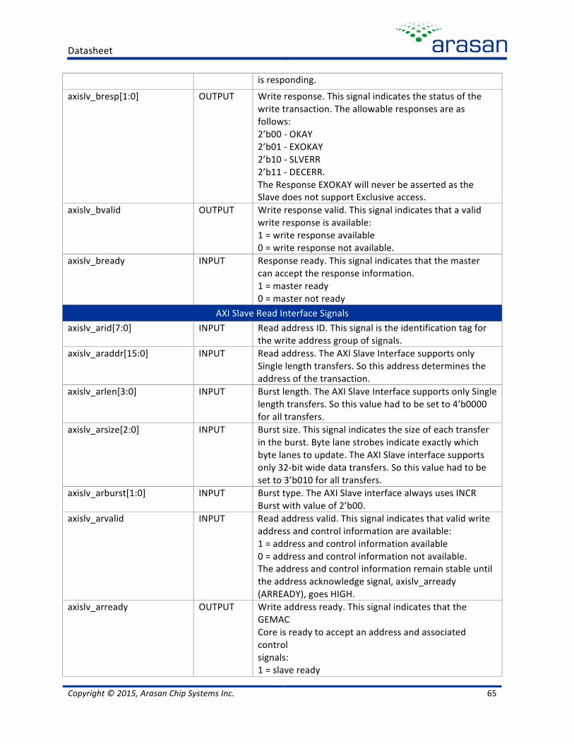
Datasheet
Copyright © 2015, Arasan Chip Systems Inc. 65
is responding.
axislv_bresp[1:0] OUTPUT Write response. This signal indicates the status of the write transaction. The allowable responses are as follows: 2’b00 -‐ OKAY 2’b01 -‐ EXOKAY 2’b10 -‐ SLVERR 2’b11 -‐ DECERR. The Response EXOKAY will never be asserted as the Slave does not support Exclusive access.
axislv_bvalid OUTPUT Write response valid. This signal indicates that a valid write response is available: 1 = write response available 0 = write response not available.
axislv_bready INPUT Response ready. This signal indicates that the master can accept the response information. 1 = master ready 0 = master not ready
AXI Slave Read Interface Signals axislv_arid[7:0] INPUT Read address ID. This signal is the identification tag for
the write address group of signals. axislv_araddr[15:0] INPUT Read address. The AXI Slave Interface supports only
Single length transfers. So this address determines the address of the transaction.
axislv_arlen[3:0] INPUT Burst length. The AXI Slave Interface supports only Single length transfers. So this value had to be set to 4’b0000 for all transfers.
axislv_arsize[2:0] INPUT Burst size. This signal indicates the size of each transfer in the burst. Byte lane strobes indicate exactly which byte lanes to update. The AXI Slave interface supports only 32-‐bit wide data transfers. So this value had to be set to 3’b010 for all transfers.
axislv_arburst[1:0] INPUT Burst type. The AXI Slave interface always uses INCR Burst with value of 2’b00.
axislv_arvalid INPUT Read address valid. This signal indicates that valid write address and control information are available: 1 = address and control information available 0 = address and control information not available. The address and control information remain stable until the address acknowledge signal, axislv_arready (ARREADY), goes HIGH.
axislv_arready OUTPUT Write address ready. This signal indicates that the GEMAC Core is ready to accept an address and associated control signals: 1 = slave ready

Datasheet
Copyright © 2015, Arasan Chip Systems Inc. 66
0 = slave not ready.
axislv_rid[7:0] OUTPUT Read ID tag. This signal is the ID tag of the read data transfer. The axislv_rid (RID) value matches the axislv_arid (ARID) value of the read transaction
aximst_rdata[31:0] OUTPUT Read data. The AXI Slave Interface supports only 32-‐bit wide data transfers on 32-‐bit wide data bus.
axislv_rresp[1:0] OUTPUT Read response. This signal indicates the status of the read transaction. The allowable responses are as follows: 2’b00 -‐ OKAY 2’b01 -‐ EXOKAY 2’b10 -‐ SLVERR 2’b11 -‐ DECERR. The Response EXOKAY should never be asserted as the Master never generates Exclusive access.
axislv_rlast OUTPUT Read last. This signal indicates the last transfer in a read burst
axislv_rvalid OUTPUT Read valid. This signal indicates that valid read data and strobes are available: 1 = read data and strobes available 0 = read data and strobes not available.
axislv_rready INPUT Read ready. This signal indicates that the Master can accept the read data: 1 = slave ready 0 = slave not ready.
Table 11: 1588 Interface Signal Descriptions
Pins Direction Description clk_1588 INPUT clk_1588 (1588 Reference Clock) is used to run the IEEE-‐
1588 Module in the GEMAC Core. The System Timer runs on this clock. This can be independent of host_clk.
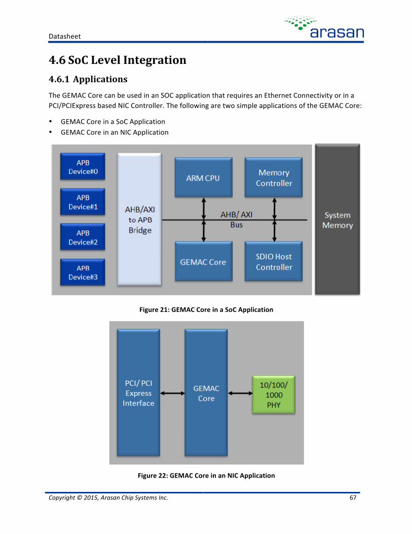
Datasheet
Copyright © 2015, Arasan Chip Systems Inc. 67
4.6 SoC Level Integration 4.6.1 Applications The GEMAC Core can be used in an SOC application that requires an Ethernet Connectivity or in a PCI/PCIExpress based NIC Controller. The following are two simple applications of the GEMAC Core:
• GEMAC Core in a SoC Application • GEMAC Core in an NIC Application
Figure 21: GEMAC Core in a SoC Application
Figure 22: GEMAC Core in an NIC Application

Datasheet
Copyright © 2015, Arasan Chip Systems Inc. 68
4.6.2 IP Deliverables The IP package consists of the following:
• RMM Compliant Synthesizable RTL design in Verilog • Easy-‐to-‐use test environment • Synthesis scripts • Technical documents

Datasheet
Copyright © 2015, Arasan Chip Systems Inc. 69
5 Ethernet Device Driver 5.1 Overview Arasan Chip Systems‘ 802.3 Ethernet Device Driver is developed to support both the 10/ 100 Ethernet IP as well as its Gigabit Ethernet IP. The device driver provides communications between the MAC (Medium Access Control) and the OS (operating System) as well as access to the overlying network layer protocol and the applications layer. The device driver provides developers a complete software solution for quick deployment of 10/100 or Gigabit Ethernet applications in a Linux based network environment. The software driver is compliant to IEEE 802.3 standards. It is written in ANSI C to facilitate quick and simple migration to multiple platforms using Arasan’s Ethernet IPs. The device driver can be used in PCs, laptop computers, portable media devices or other compatible embedded systems using Arasan’s Ethernet IPs.
To facilitate the development of new network systems, the Arasan Ethernet Linux Device Driver supports a Windows based Ethereal tool for network packet analysis, and a FTP Client WinScp for handling file transfer between Windows and Linux systems. The Gigabit Ethernet Linux Driver is a PCI based network device driver that the system uses it to communicate with the PCI-‐Ethernet network card and provides a network interface to the system.
5.2 Features • Supports: Arasan Gigabit Ethernet and 10/100 Ethernet IP Cores • Designed and developed to be fully integrated with the Linux OS Fedora Core 6.0 • Written in ANSI C for portability • Modular design • OS abstraction layer • Hardware abstraction layer • Supports full speed Ethernet up to 10/100Mbps and • 1 Gbps data rates • Implemented and tested with Arasan IPcores and FPGA platform • Supports Ethereal for debugging • Supports Ipref for throughput analysis • Supports remote debugging • Scatter Gather DMA to minimize CPU load • Low number of interrupt processing results in power saving in system level
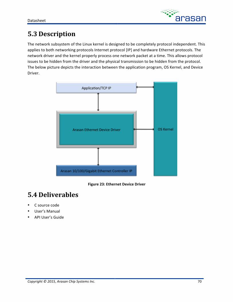
Datasheet
Copyright © 2015, Arasan Chip Systems Inc. 70
5.3 Description The network subsystem of the Linux kernel is designed to be completely protocol independent. This applies to both networking protocols Internet protocol [IP] and hardware Ethernet protocols. The network driver and the kernel properly process one network packet at a time. This allows protocol issues to be hidden from the driver and the physical transmission to be hidden from the protocol. The below picture depicts the interaction between the application program, OS Kernel, and Device Driver.
Figure 23: Ethernet Device Driver
5.4 Deliverables • C source code • User’s Manual • API User’s Guide

Datasheet
Copyright © 2015, Arasan Chip Systems Inc. 71
6 Services & Support 6.1 Global Support Arasan Chip Systems provide global support to its IP customers. The technical support is not geographically bound to any specific site or location, and therefore our customers can easily get support for design teams that are distributed in several locations at no extra cost.
6.2 Arasan Support Team Our technical support is provided by the engineers who have designed the IP. That is a huge benefit for our customers, who can communicate directly with the engineers who have the deepest knowledge and domain expertise of the IP, and the standard to which it complies.
6.3 Professional Services & Customization At Arasan Chip Systems we understand that no two Application Processors are the same. We realize that often the standard itself needs some tweaks and optimizations to fit your design better. Sometimes, the interface between the IP blocks and your design need some customization. Therefore, we provide professional services and customization to our IP customers. We do not sell our IP blocks as “black box” that cannot be touched. Please contact us for more details on our customization services.
6.4 The Arasan Porting Engine Analog IP blocks, such as eMMC 5.1 HS400 PHY, are designed for a specific Fab and process technology. Arasan’s analog design team, utilizing its deep domain expertise and vast experience, is capable of porting the PHYs into any specific process technology required by the customer. That is “The Arasan Porting Engine”.
6.5 Pricing & Licensing Arasan charges a one-‐time licensing fee, with no additional royalties. The licensing fee gives the right to use our IP for 1 project. Licensing fee for additional projects, using the same IP, is discounted. We also offer unlimited-‐use license. For any additional information regarding pricing and licensing – please contact our sales at: [email protected].