Embed Size (px)
Citation preview
3D & 2½D Test Challenges Getting to Known Good Die
& Known Good Stack
Gary Fleeman Advantest Corporation
1.22.2013 Gary Fleeman 1
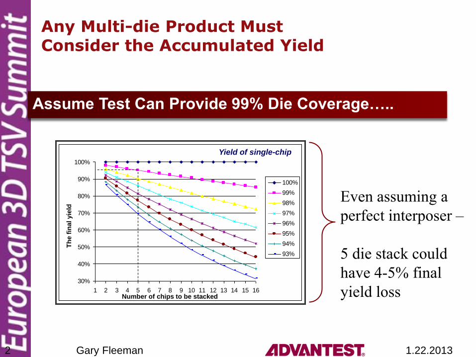
Any Multi-die Product Must Consider the Accumulated Yield
Even assuming a
perfect interposer –
5 die stack could
have 4-5% final
yield loss 30%
40%
50%
60%
70%
80%
90%
100%
1 2 3 4 5 6 7 8 9 10 11 12 13 14 15 16
100%
99%
98%
97%
96%
95%
94%
93%
Th
e f
inal yie
ld
Yield of single-chip
Number of chips to be stacked
Assume Test Can Provide 99% Die Coverage…..
1.22.2013 Gary Fleeman 2
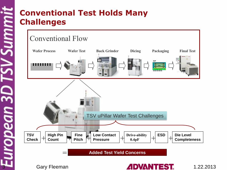
Wafer Process Wafer Test Back Grinder Dicing Packaging Final Test
Conventional Flow
Drive-ability
0.4pF
High Pin
Count
Fine
Pitch
Low Contact
Pressure
TSV uPillar Wafer Test Challenges
Die Level
Completeness
TSV
Check
ESD
+ + + + + +
Added Test Yield Concerns =
Conventional Test Holds Many Challenges
1.22.2013 Gary Fleeman 3
Test Challenges
1.22.2013 Gary Fleeman 4
Drive-ability
High Pin
Count
Fine
Pitch
Low Contact
Pressure
Die Level
Completeness
TSV
Check
ESD
Limitation: - Lowest cost device(can’t afford to test); no access until after thin.
Countermeasures: - Very good yields; parametric samples, visual & Xray inspections.
Issues: - PPM can have big effect. And … Active interposers are coming.
+ + + + + +
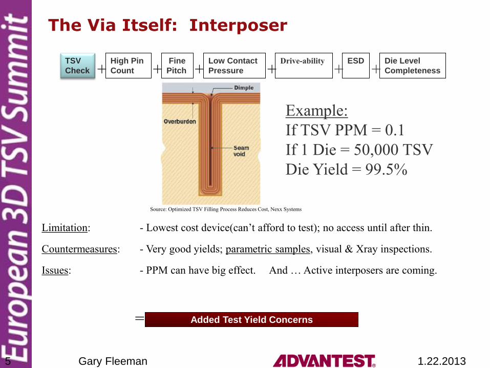
Source: Optimized TSV Filling Process Reduces Cost, Nexx Systems
Example:
If TSV PPM = 0.1
If 1 Die = 50,000 TSV
Die Yield = 99.5%
The Via Itself: Interposer
Added Test Yield Concerns =
1.22.2013 Gary Fleeman 5
Drive-ability
High Pin
Count
Fine
Pitch
Low Contact
Pressure
Die Level
Completeness
TSV
Check
ESD
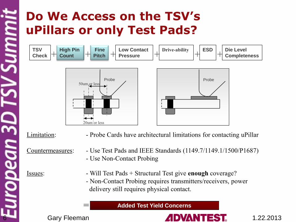
Limitation: - Probe Cards have architectural limitations for contacting uPillar
Countermeasures: - Use Test Pads and IEEE Standards (1149.7/1149.1/1500/P1687)
- Use Non-Contact Probing
Issues: - Will Test Pads + Structural Test give enough coverage?
- Non-Contact Probing requires transmitters/receivers, power
delivery still requires physical contact.
+ + + + + +
50um or less
20um or less
Probe
Do We Access on the TSV’s uPillars or only Test Pads?
Added Test Yield Concerns
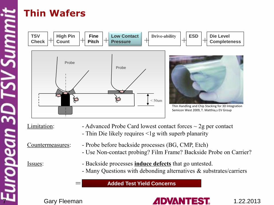
Probe
=
1.22.2013 Gary Fleeman 6
Drive-ability
High Pin
Count
Fine
Pitch
Low Contact
Pressure
Die Level
Completeness
TSV
Check
ESD
Probe
< 50um
Limitation: - Advanced Probe Card lowest contact forces ~ 2g per contact
- Thin Die likely requires <1g with superb planarity
Countermeasures: - Probe before backside processes (BG, CMP, Etch)
- Use Non-contact probing? Film Frame? Backside Probe on Carrier?
Issues: - Backside processes induce defects that go untested.
- Many Questions with debonding alternatives & substrates/carriers
+ + + + + +
Thin Wafers
Added Test Yield Concerns =
Probe
Thin Handling and Chip Stacking for 3D Integration Semicon West 2009, T. Matthia,s EV Group
1.22.2013 Gary Fleeman 7
Drive-ability
High Pin
Count
Fine
Pitch
Low Contact
Pressure
Die Level
Completeness
TSV
Check
ESD
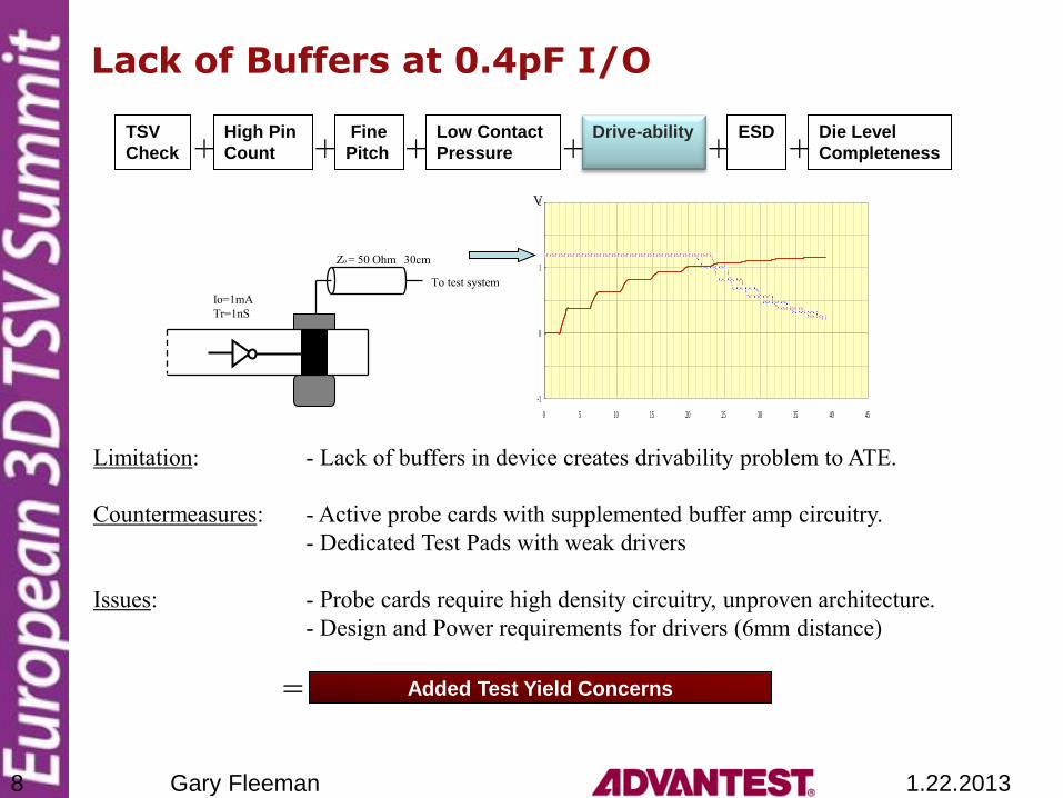
Limitation: - Lack of buffers in device creates drivability problem to ATE.
Countermeasures: - Active probe cards with supplemented buffer amp circuitry.
- Dedicated Test Pads with weak drivers
Issues: - Probe cards require high density circuitry, unproven architecture.
- Design and Power requirements for drivers (6mm distance)
+ + + + + +
Lack of Buffers at 0.4pF I/O
Added Test Yield Concerns
-1
0
1
2
0 5 10 15 20 25 30 35 40 45
Z0 = 50 Ohm 30cm
To test system
Io=1mA
Tr=1nS
V
=
1.22.2013 Gary Fleeman 8
Drive-ability
High Pin
Count
Fine
Pitch
Low Contact
Pressure
Die Level
Completeness
TSV
Check
ESD
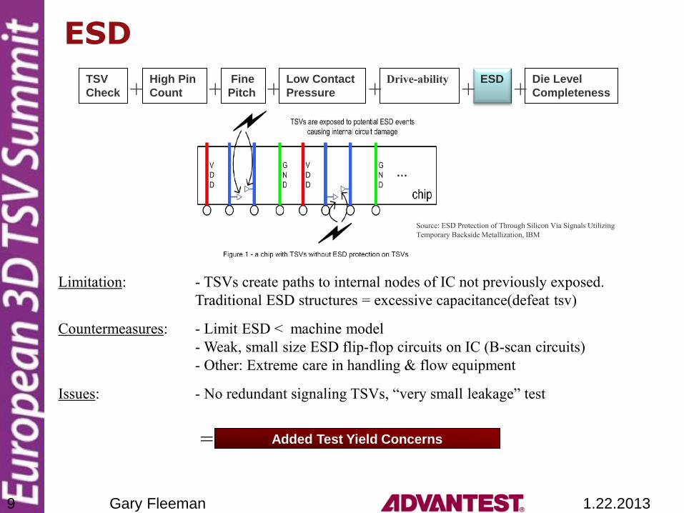
Limitation: - TSVs create paths to internal nodes of IC not previously exposed.
Traditional ESD structures = excessive capacitance(defeat tsv)
Countermeasures: - Limit ESD < machine model
- Weak, small size ESD flip-flop circuits on IC (B-scan circuits)
- Other: Extreme care in handling & flow equipment
Issues: - No redundant signaling TSVs, “very small leakage” test
+ + + + + +
Source: ESD Protection of Through Silicon Via Signals Utilizing
Temporary Backside Metallization, IBM
ESD
Added Test Yield Concerns =
1.22.2013 Gary Fleeman 9
Drive-ability
High Pin
Count
Fine
Pitch
Low Contact
Pressure
Die Level
Completeness
TSV
Check
ESD
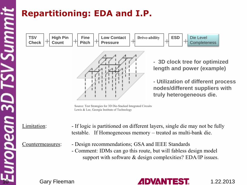
Limitation: - If logic is partitioned on different layers, single die may not be fully
testable. If Homogeneous memory – treated as multi-bank die.
Countermeasures: - Design recommendations; GSA and IEEE Standards
- Comment: IDMs can go this route, but will fabless design model
support with software & design complexities? EDA/IP issues.
+ + + + + +
- 3D clock tree for optimized
length and power (example)
- Utilization of different process
nodes/different suppliers with
truly heterogeneous die.
Source: Test Strategies for 3D Die-Stacked Integrated Circuits
Lewis & Lee, Georgia Institute of Technology
Repartitioning: EDA and I.P.
1.22.2013 Gary Fleeman 10
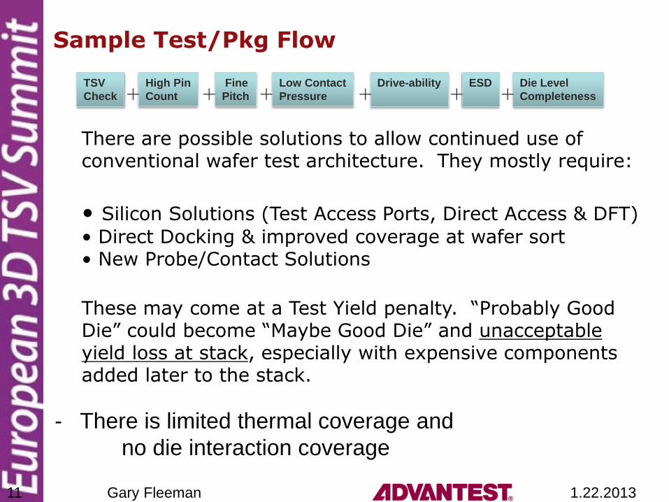
There are possible solutions to allow continued use of conventional wafer test architecture. They mostly require:
• Silicon Solutions (Test Access Ports, Direct Access & DFT)
• Direct Docking & improved coverage at wafer sort • New Probe/Contact Solutions
These may come at a Test Yield penalty. “Probably Good Die” could become “Maybe Good Die” and unacceptable yield loss at stack, especially with expensive components added later to the stack.
Drive-ability
High Pin
Count
Fine
Pitch
Low Contact
Pressure
Die Level
Completeness
TSV
Check
ESD
+ + + + + +
Sample Test/Pkg Flow
- There is limited thermal coverage and
no die interaction coverage
1.22.2013 Gary Fleeman 11
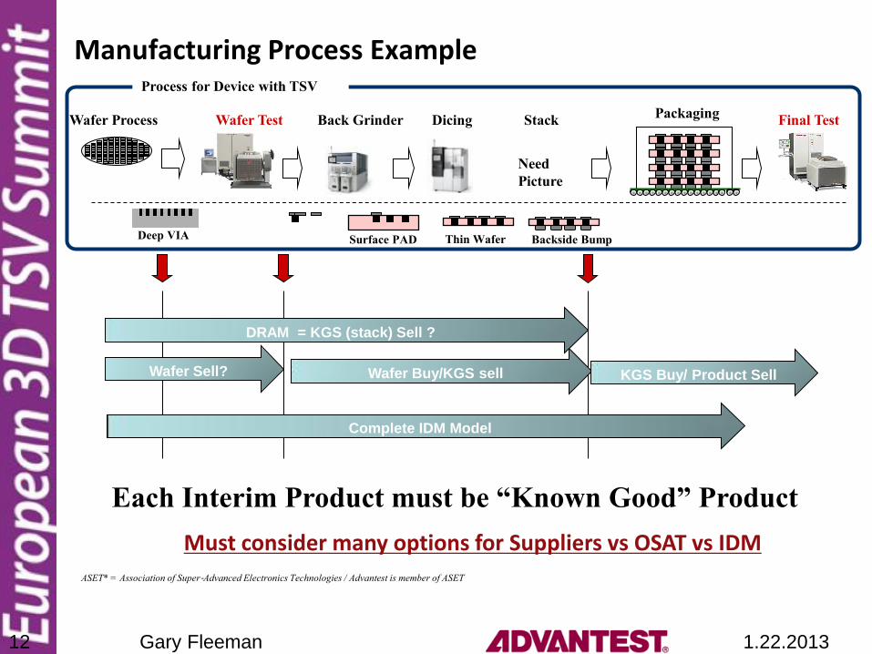
Manufacturing Process Example
Wafer Process Wafer Test Back Grinder Dicing Packaging
Final Test
Process for Device with TSV
Deep VIA Thin Wafer Backside Bump Surface PAD
ASET* = Association of Super‐Advanced Electronics Technologies / Advantest is member of ASET
Stack
Need
Picture
Wafer Sell? Wafer Buy/KGS sell KGS Buy/ Product Sell
Must consider many options for Suppliers vs OSAT vs IDM
Each Interim Product must be “Known Good” Product
DRAM = KGS (stack) Sell ?
Complete IDM Model
1.22.2013 Gary Fleeman 12
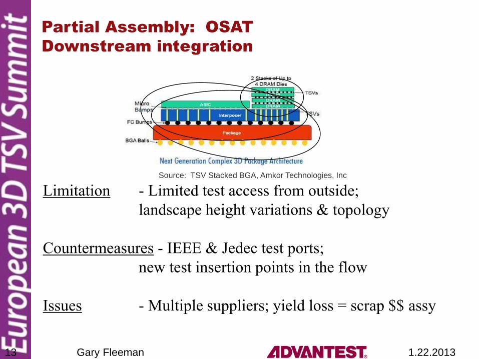
Limitation - Limited test access from outside;
landscape height variations & topology
Countermeasures - IEEE & Jedec test ports;
new test insertion points in the flow
Issues - Multiple suppliers; yield loss = scrap $$ assy
Partial Assembly: OSAT
Downstream integration
Source: TSV Stacked BGA, Amkor Technologies, Inc
1.22.2013 Gary Fleeman 13
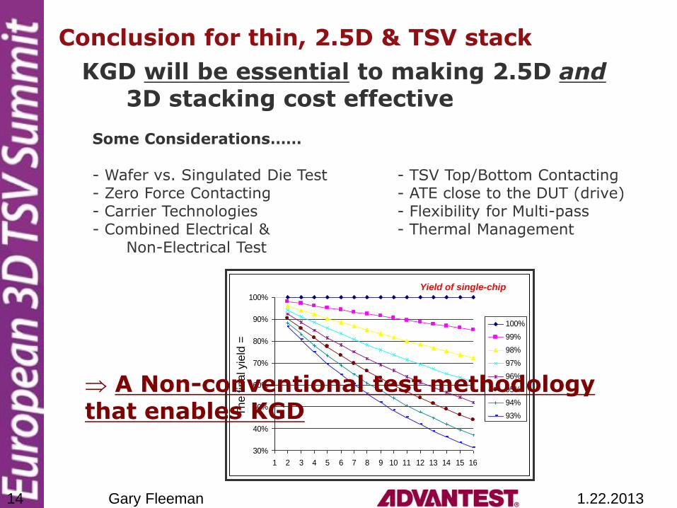
KGD will be essential to making 2.5D and 3D stacking cost effective
Some Considerations……
- Wafer vs. Singulated Die Test - TSV Top/Bottom Contacting - Zero Force Contacting - ATE close to the DUT (drive) - Carrier Technologies - Flexibility for Multi-pass - Combined Electrical & - Thermal Management Non-Electrical Test
Conclusion for thin, 2.5D & TSV stack
30%
40%
50%
60%
70%
80%
90%
100%
1 2 3 4 5 6 7 8 9 10 11 12 13 14 15 16
100%
99%
98%
97%
96%
95%
94%
93%Th
e fin
al yie
ld =
Yield of single-chip
A Non-conventional test methodology that enables KGD
1.22.2013 Gary Fleeman 14
Commodity Success Challenge
• MUST achieve cost targets even though there is value added with reliability and KGD.
• Supply chain management gets complicated. » Who is responsible for 3D/2.5D/TSV quality/yield? » KGD guaranteed ? How?
• Manufacturing process depends on business model What sequence, where’s the failure or faults, etc.
1.22.2013 Gary Fleeman 15
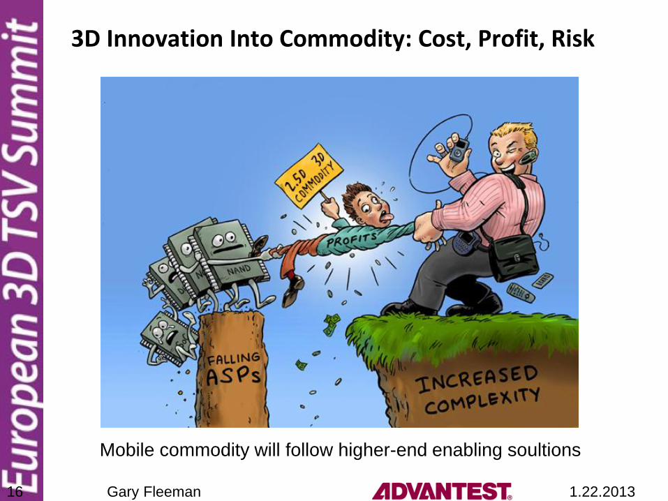
3D Innovation Into Commodity: Cost, Profit, Risk
Mobile commodity will follow higher-end enabling soultions
1.22.2013 Gary Fleeman 16
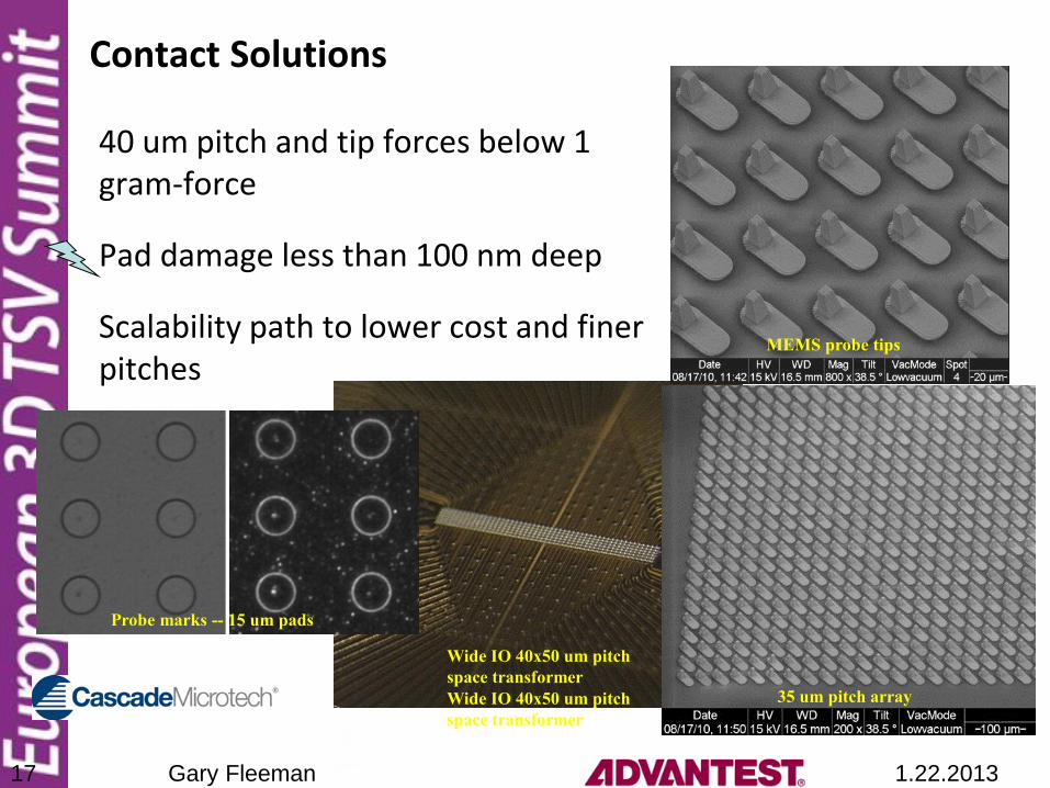
40 um pitch and tip forces below 1 gram-force
Pad damage less than 100 nm deep
Scalability path to lower cost and finer pitches
Wide IO 40x50 um pitch
space transformer
Contact Solutions
Probe marks -- 15 um pads
MEMS probe tips
Wide IO 40x50 um pitch
space transformer
35 um pitch array
1.22.2013 Gary Fleeman 17
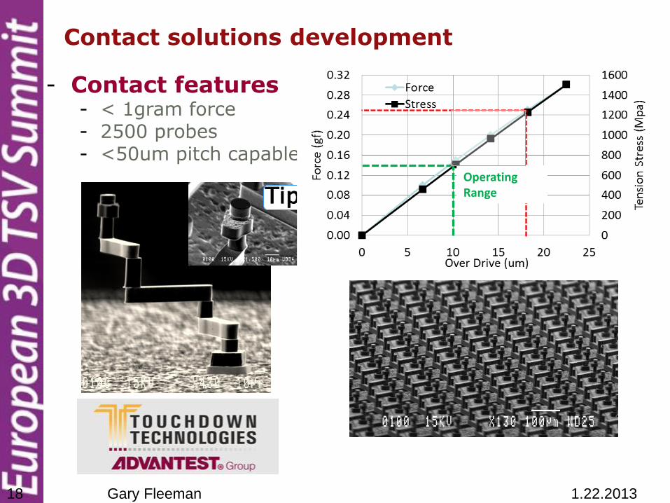
- Contact features - < 1gram force - 2500 probes - <50um pitch capable
Tip
Contact solutions development
Operating Range
1.22.2013 Gary Fleeman 18
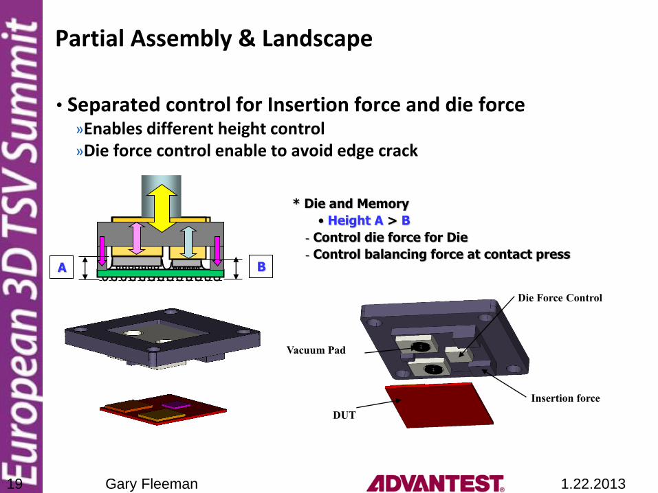
Partial Assembly & Landscape
• Separated control for Insertion force and die force »Enables different height control »Die force control enable to avoid edge crack
Vacuum Pad
DUT
Die Force Control
Insertion force
B A
* Die and Memory
• Height A > B
- Control die force for Die
- Control balancing force at contact press
1.22.2013 Gary Fleeman 19
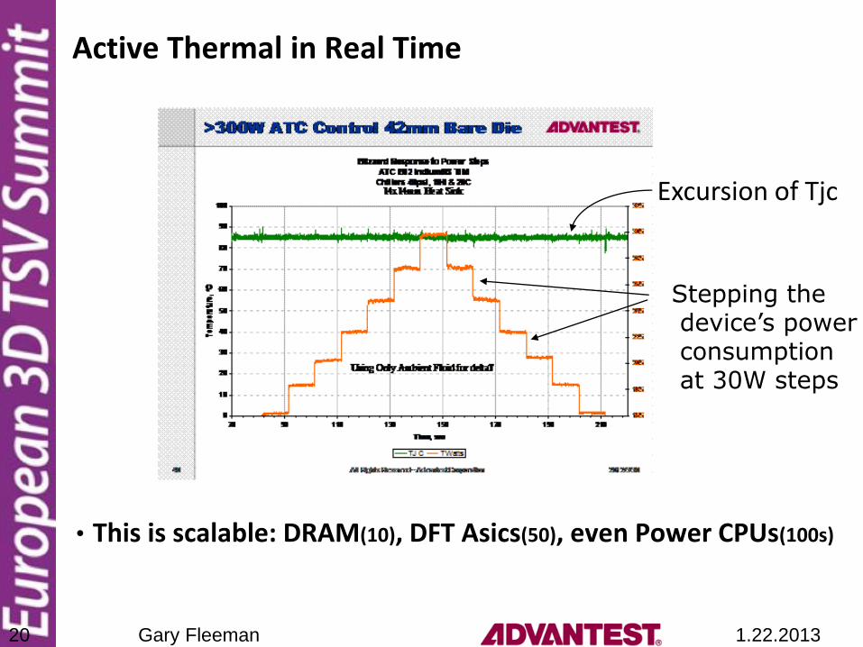
Active Thermal in Real Time
• This is scalable: DRAM(10), DFT Asics(50), even Power CPUs(100s)
Excursion of Tjc
Stepping the device’s power consumption at 30W steps
1.22.2013 Gary Fleeman 20
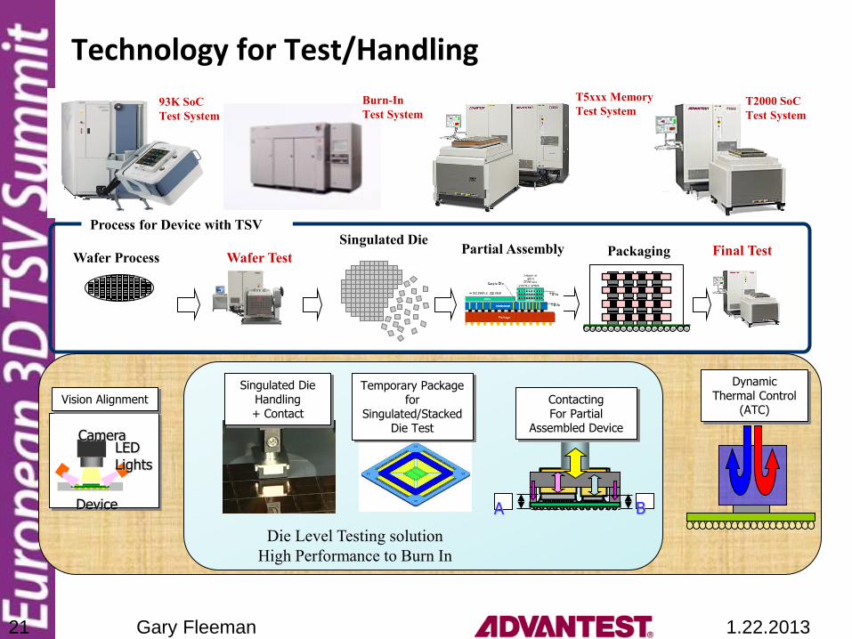
Technology for Test/Handling
Wafer Process Wafer Test
Singulated Die Final Test Packaging
Process for Device with TSV
T2000 SoC
Test System
T5xxx Memory
Test System 93K SoC
Test System
Camera LED Lights
Device
Vision Alignment Singulated Die
Handling + Contact
Temporary Package for
Singulated/Stacked Die Test
Die Level Testing solution
High Performance to Burn In
B A
Contacting For Partial
Assembled Device
Dynamic Thermal Control
(ATC)
Partial Assembly
Burn-In
Test System
1.22.2013 Gary Fleeman 21
• New test points – IEEE, Semi, IMEC Erik Jan and team – Many new test points- but they will be selectively implemented – Each flow will use different points; No flow will use all points
• Optimized flows and test economy
• Key is tooling flexibility & integration
• Yield, Yield, YIELD
Summary for 2.5D & 3D Test
1.22.2013 Gary Fleeman 22
Thanks & Merci beaucoup
1.22.2013 Gary Fleeman 23
Coming 2.5D and 3D products pose new challenges to the production test environment. Providing a
commodity viable 3D product demands implementation of unique test and handling solutions. Yield is
the foremost concern but cost sensitivity and test economics are critical to any successful commodity.
Manufacturing (back end) flows and new insertion points will be described. The presentation will also
outline challenges of 2.5D and 3D implementation, highlight limitations with today's monolithic
solutions, and offer alternatives for a high yield, integrated Die Level Handling environment.
1.22.2013 Gary Fleeman 24


![RESEARCH Open Access Respiratory chain complex III ... · (c.232A>G; p.Ser78Gly) [14], with over 40 known cases. Since these patients die early in life, little is known about their](https://img.pdfslide.us/doc/110x75/60a27acced75ce75b1249c8e/research-open-access-respiratory-chain-complex-iii-c232ag-pser78gly.jpg)