Embed Size (px)
DESCRIPTION
Getting the O in I/O to work on a typical microcontroller. Activating a FLASH memory “output line” Part 1 Main part of Laboratory 1 Also needed for “voice activated car control project”. Agenda. Processors need to send out control signals (high / low 1 / 0 true / false) - PowerPoint PPT Presentation
Citation preview

Getting the O in I/O to workon a typical microcontroller
Activating a FLASH memory “output line”Part 1
Main part of Laboratory 1Also needed for “voice activated car control project”

Agenda• Processors need to send out control
signals (high / low 1 / 0 true / false)
– General purpose input / output lines (GPIO lines) on processor chip (16)
– FLASH memory chip has additional I/O ports connected to Ez-Lite KIT LED’s
• What do we need to have happen to make the FLASH memory work on a microcontroller as we want. (In this example turning the board LED’s on and off)
• What new Blackfin assembly language instructions do we need to learn in order to operate the LEDs?
Blackfin BF533 I/O 2

Programmable Flags• Most micro-controllers have general
purpose input or output lines capable of generating “true” or “false” values
• Blackfin 533 has 16 GPIO lines
Blackfin BF533 I/O 3
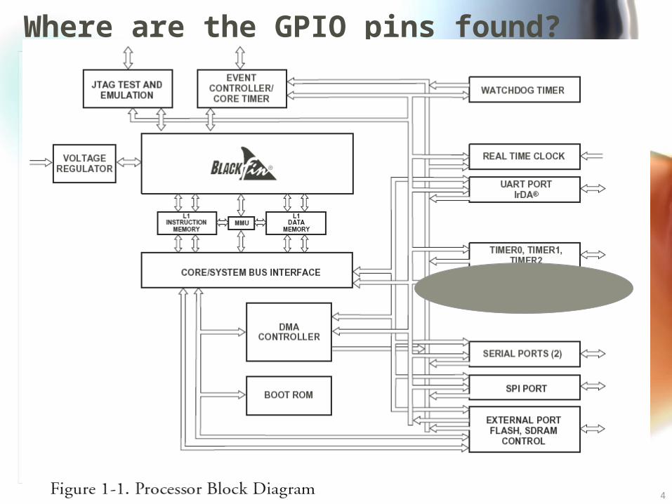
Where are the GPIO pins found?
Blackfin BF533 I/O 4
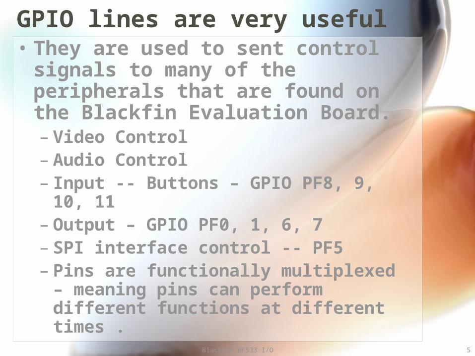
GPIO lines are very useful• They are used to sent control signals
to many of the peripherals that are found on the Blackfin Evaluation Board.– Video Control– Audio Control– Input -- Buttons – GPIO PF8, 9, 10, 11 – Output – GPIO PF0, 1, 6, 7– SPI interface control -- PF5– Pins are functionally multiplexed –
meaning pins can perform different functions at different times .
Blackfin BF533 I/O 5
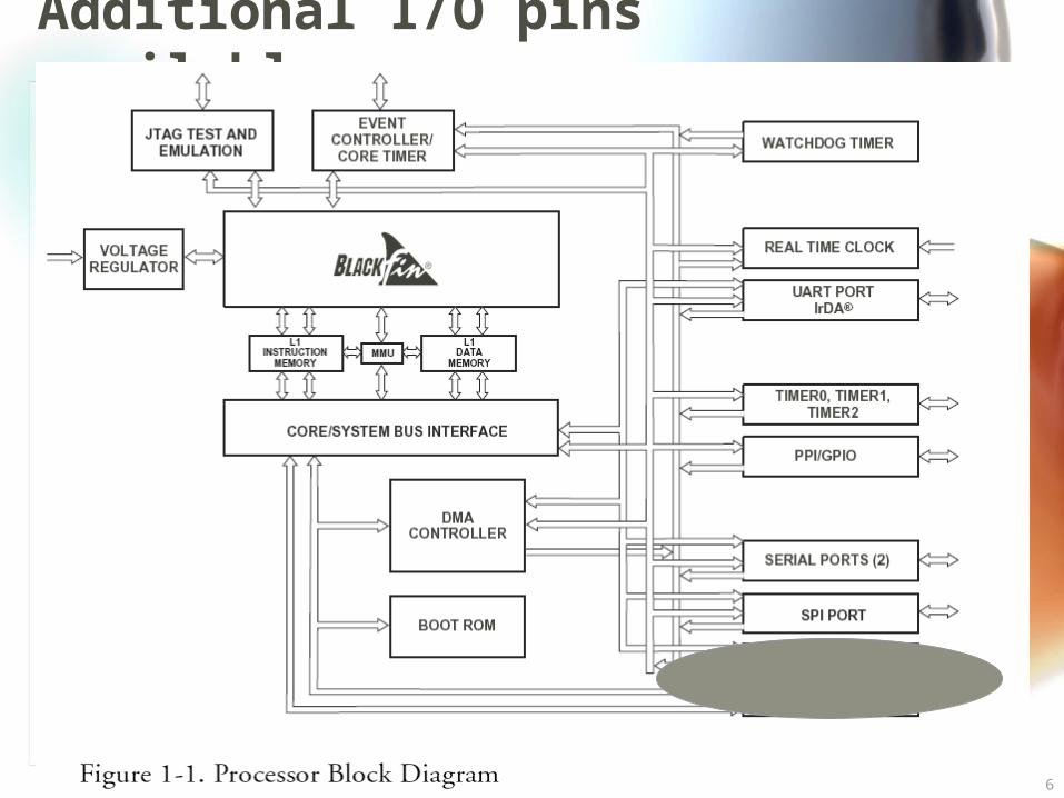
Additional I/O pins available
Blackfin BF533 I/O 6
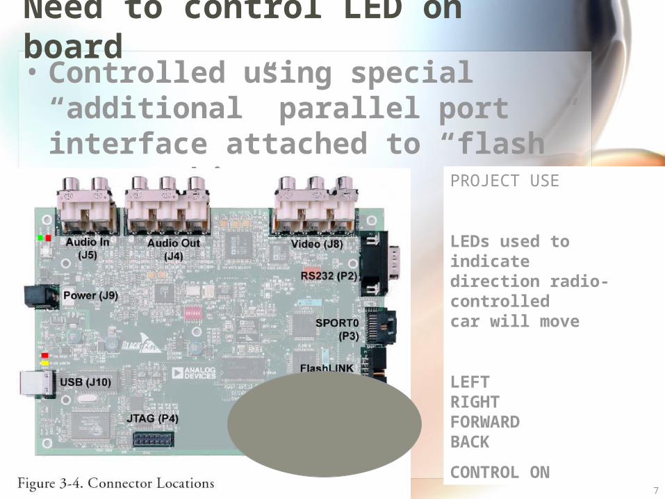
Need to control LED on board• Controlled using special “additional”
parallel port interface attached to “flash” memory chip
Blackfin BF533 I/O 7
PROJECT USE
LEDs used to indicatedirection radio-controlledcar will move
LEFTRIGHTFORWARDBACK
CONTROL ON
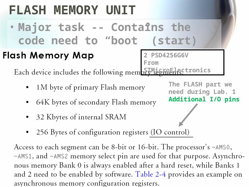
FLASH MEMORY UNIT• Major task -- Contains the code need
to “boot” (start) the processor
Blackfin BF533 I/O 8
2 PSD4256G6VFrom STMicroElectronics
The FLASH part we need during Lab. 1Additional I/O pins
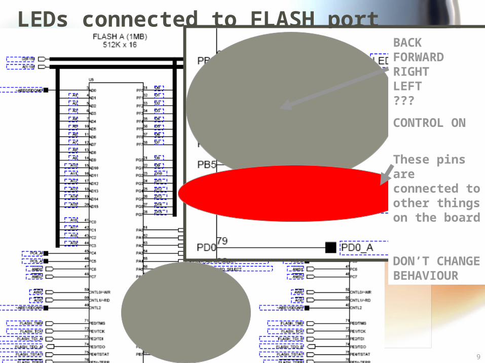
LEDs connected to FLASH port
Blackfin BF533 I/O 9
BACKFORWARDRIGHTLEFT???
CONTROL ON
These pins are connected to other things on the board
DON’T CHANGEBEHAVIOUR

Steps to activating LEDs• Get the FLASH memory to work
correctly– Write the code for InitFlashASM( )
• Get the Port to work correctly as output for pins PB5 PB0, leaving other pins unchanged– Write the code for InitFlashPortASM( )
• Write the value we want to LEDs– WriteFlashLEDASM( int value)
• Read back the value the LEDs show– int ReadFlashLEDASM( )
Blackfin BF533 I/O 10

FLASH MEMORY UNIT• Controlled through “EBIU”
External Bus Interface UnitEBIU are common on most processors (although often by different name)
Blackfin BF533 I/O 11
FLASH
SDRAMCONTROLLER

Key information about EBIU• Three busses come into the EBIU
from the Blackfin processor core
• Forwards data to SDRAM and FLASH– How does EBIU “know” whether data is
to go to FLASH or SDRAM units?????
Blackfin BF533 I/O 12
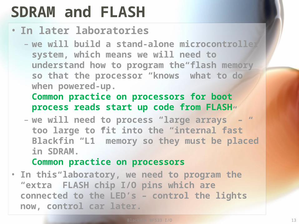
SDRAM and FLASH• In later laboratories
– we will build a stand-alone microcontroller system, which means we will need to understand how to program the flash memory so that the processor “knows” what to do when powered-up. Common practice on processors for boot process reads start up code from FLASH
– we will need to process “large arrays” – too large to fit into the “internal fast” Blackfin “L1” memory so they must be placed in SDRAM.Common practice on processors
• In this laboratory, we need to program the “extra” FLASH chip I/O pins which are connected to the LED’s – control the lights now, control car later.
Blackfin BF533 I/O 13
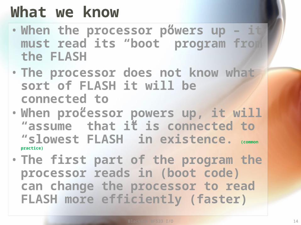
What we know• When the processor powers up – it
must read its “boot” program from the FLASH
• The processor does not know what sort of FLASH it will be connected to
• When processor powers up, it will “assume” that it is connected to “slowest FLASH” in existence. (common practice)
• The first part of the program the processor reads in (boot code) can change the processor to read FLASH more efficiently (faster)
Blackfin BF533 I/O 14
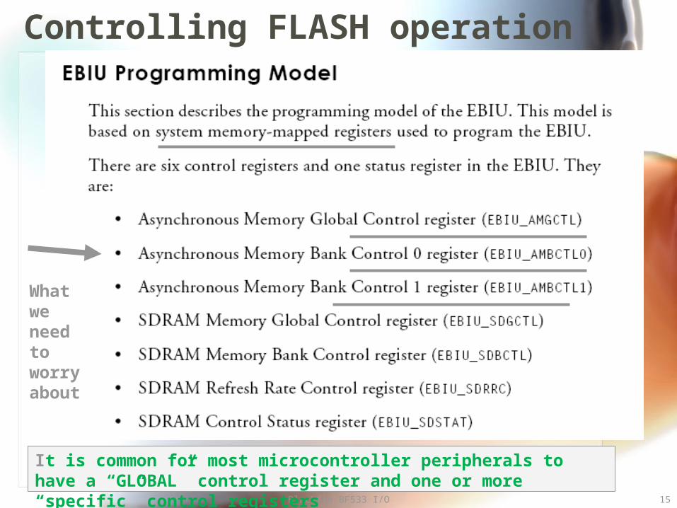
Controlling FLASH operation
Blackfin BF533 I/O 15
What we need to worry about
It is common for most microcontroller peripherals to have a “GLOBAL” control register and one or more “specific” control registers
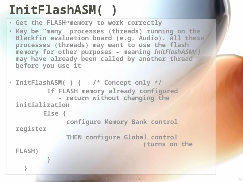
InitFlashASM( )• Get the FLASH memory to work correctly• May be “many” processes (threads) running on the
Blackfin evaluation board (e.g. Audio). All these processes (threads) may want to use the flash memory for other purposes – meaning InitFlashASM( ) may have already been called by another thread before you use it
• InitFlashASM( ) { /* Concept only */ If FLASH memory already configured
– return without changing the initialization Else { configure Memory Bank control register THEN configure Global control
(turns on the FLASH) } }
Blackfin BF533 I/O 16
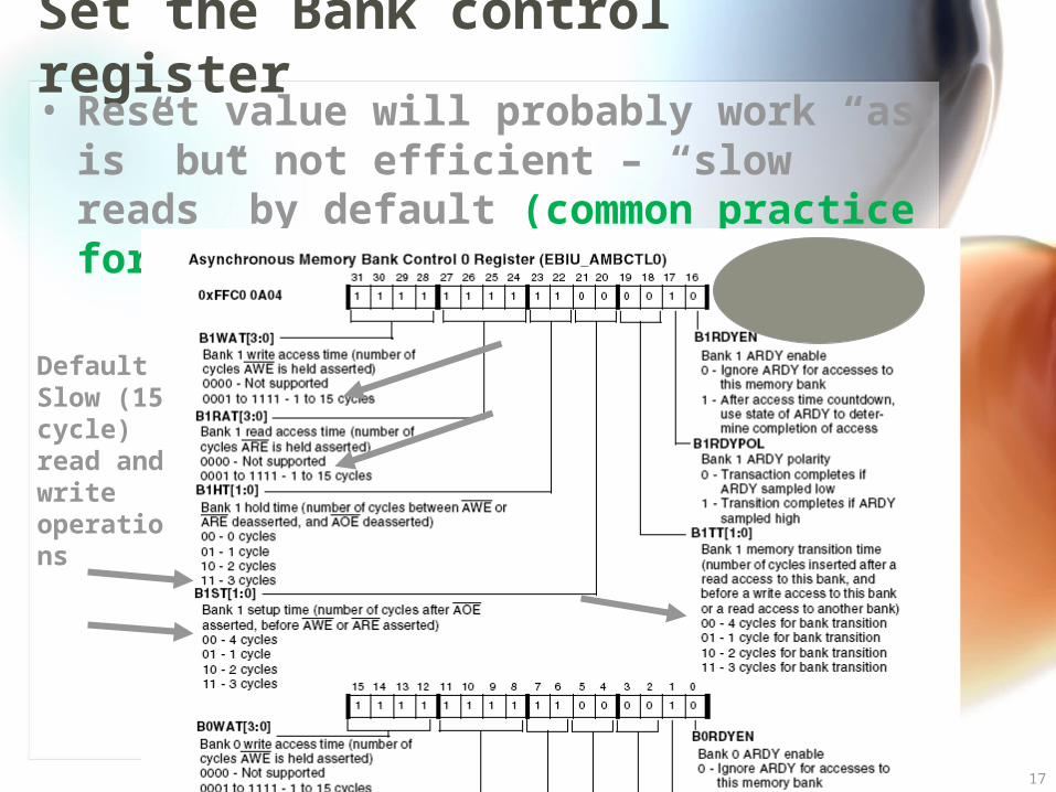
Set the Bank control register• Reset value will probably work “as is” but
not efficient – “slow reads” by default (common practice for hardware)
Blackfin BF533 I/O 17
DefaultSlow (15 cycle) read and write operations
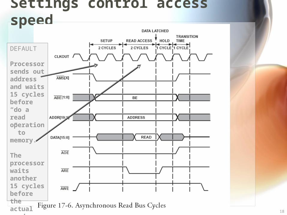
Settings control access speed
Blackfin BF533 I/O 18
DEFAULT
Processor sends out address and waits 15 cycles before “do a read operation” to memory.
The processor waits another 15 cycles before the actual read occurs.

Set General Control Register• Reset value leaves “CLKOUT”
disabled – is that important?
Blackfin BF533 I/O 19
What parts of the operation of this register must we “know”
Unanswered at this time. We don’t know what needs to be known
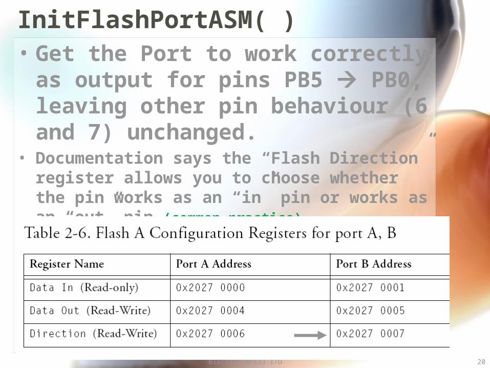
InitFlashPortASM( )• Get the Port to work correctly as
output for pins PB5 PB0, leaving other pin behaviour (6 and 7) unchanged.
• Documentation says the “Flash Direction” register allows you to choose whether the pin works as an “in” pin or works as an “out” pin (common practice)
Blackfin BF533 I/O 20
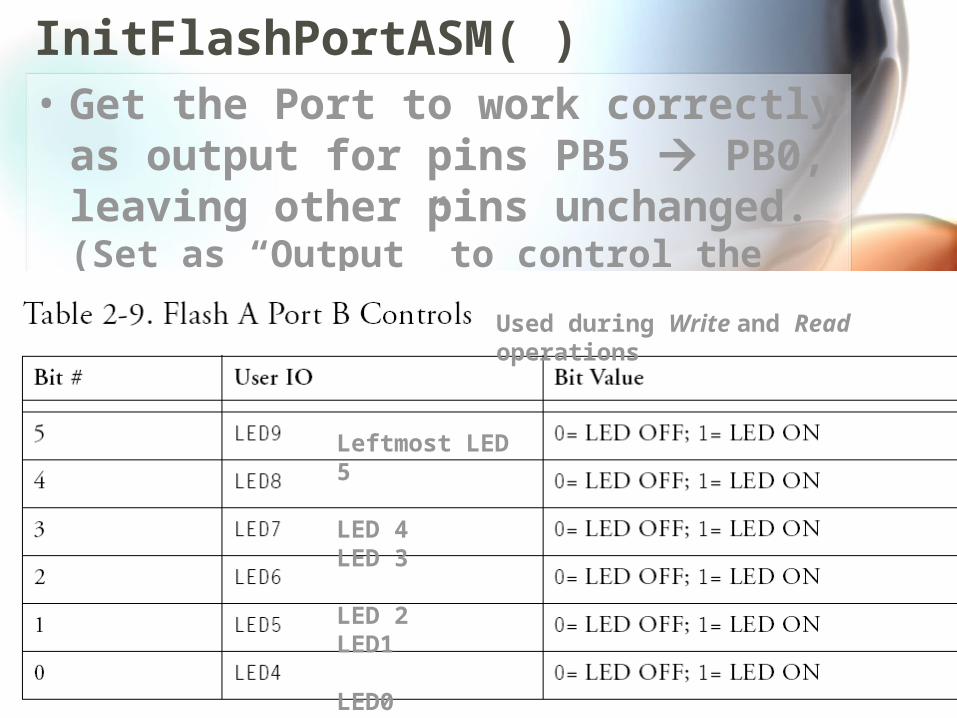
InitFlashPortASM( )• Get the Port to work correctly as
output for pins PB5 PB0, leaving other pins unchanged. (Set as “Output” to control the lights)
Blackfin BF533 I/O 21
Used during Write and Read operations
Leftmost LED 5
LED 4LED 3
LED 2LED1
LED0
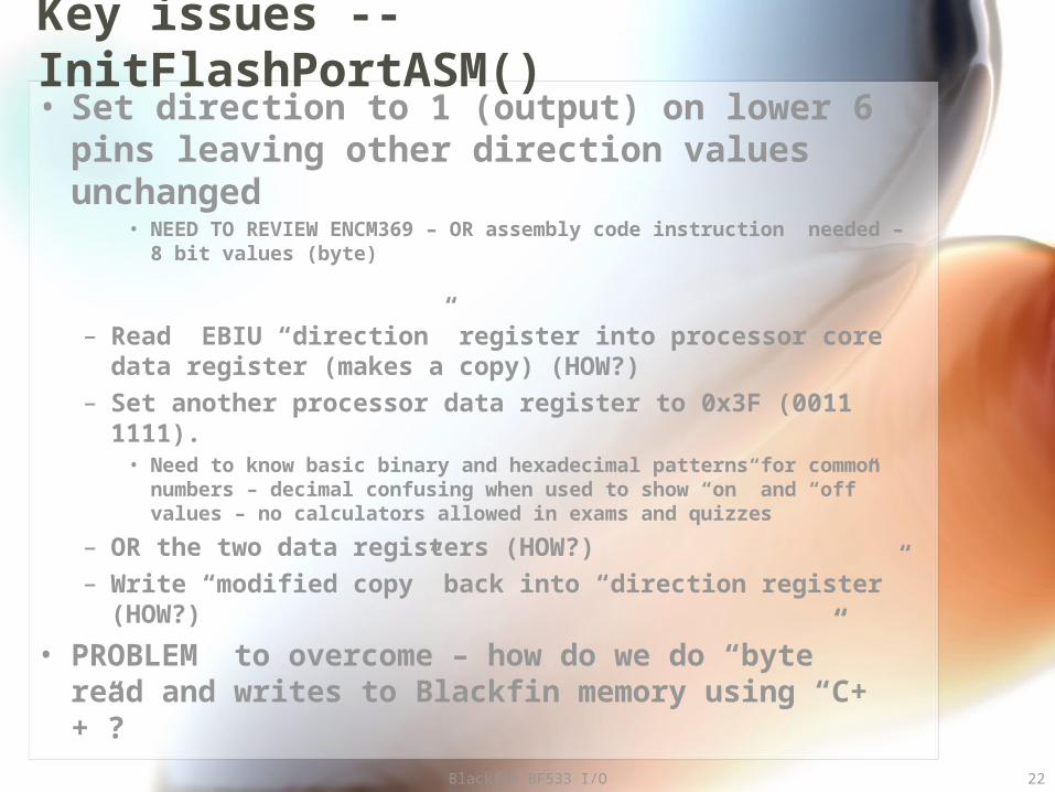
Key issues -- InitFlashPortASM()• Set direction to 1 (output) on lower 6 pins
leaving other direction values unchanged• NEED TO REVIEW ENCM369 – OR assembly code instruction
needed – 8 bit values (byte)
– Read EBIU “direction” register into processor core data register (makes a copy) (HOW?)
– Set another processor data register to 0x3F (0011 1111). • Need to know basic binary and hexadecimal patterns for common
numbers – decimal confusing when used to show “on” and “off” values – no calculators allowed in exams and quizzes
– OR the two data registers (HOW?)– Write “modified copy” back into “direction register”
(HOW?)
• PROBLEM to overcome – how do we do “byte” read and writes to Blackfin memory using “C++”?
Blackfin BF533 I/O 22
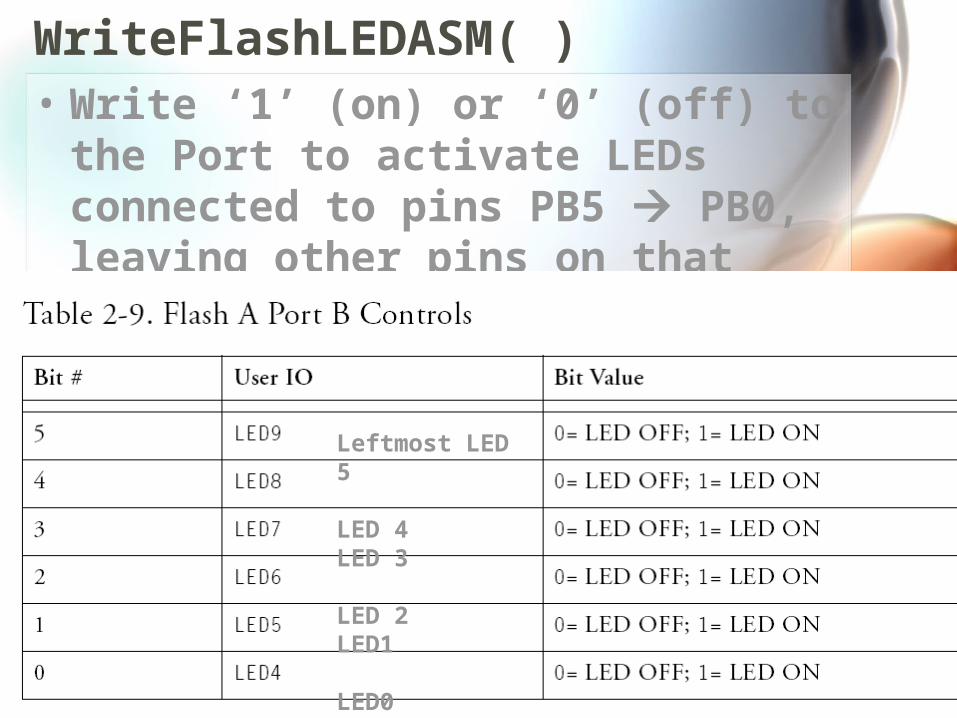
WriteFlashLEDASM( )• Write ‘1’ (on) or ‘0’ (off) to the Port to
activate LEDs connected to pins PB5 PB0, leaving other pins on that port unchanged in value. (common practice)
Blackfin BF533 I/O 23
Leftmost LED 5
LED 4LED 3
LED 2LED1
LED0
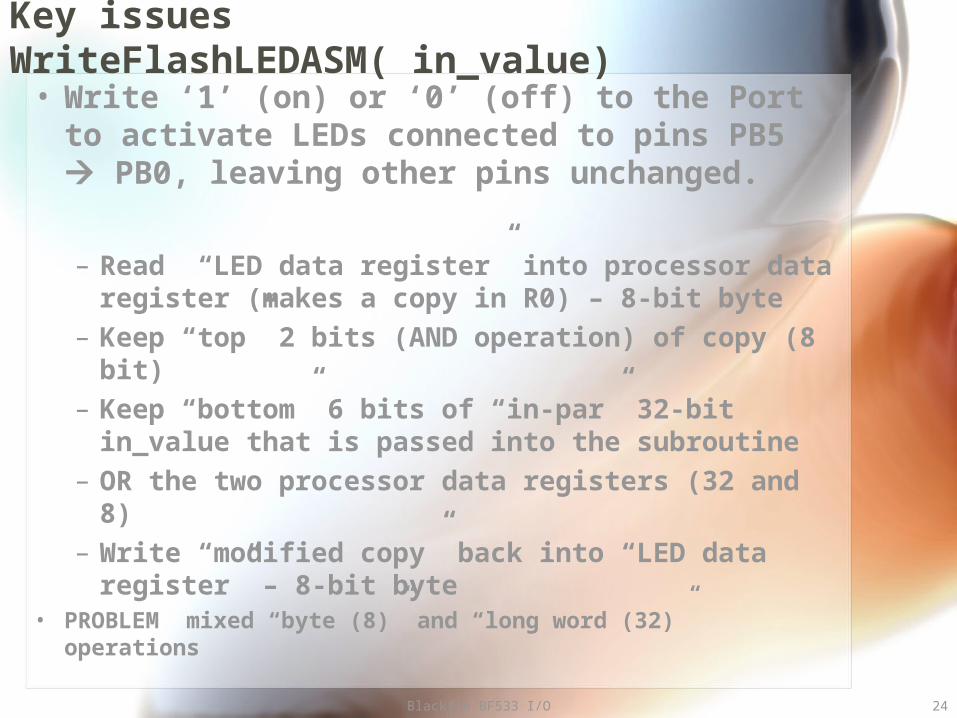
Key issues WriteFlashLEDASM( in_value)
• Write ‘1’ (on) or ‘0’ (off) to the Port to activate LEDs connected to pins PB5 PB0, leaving other pins unchanged.
– Read “LED data register” into processor data register (makes a copy in R0) – 8-bit byte
– Keep “top” 2 bits (AND operation) of copy (8 bit)– Keep “bottom” 6 bits of “in-par” 32-bit in_value
that is passed into the subroutine– OR the two processor data registers (32 and 8)– Write “modified copy” back into “LED data
register” – 8-bit byte• PROBLEM mixed “byte (8)” and “long word (32)” operations
Blackfin BF533 I/O 24
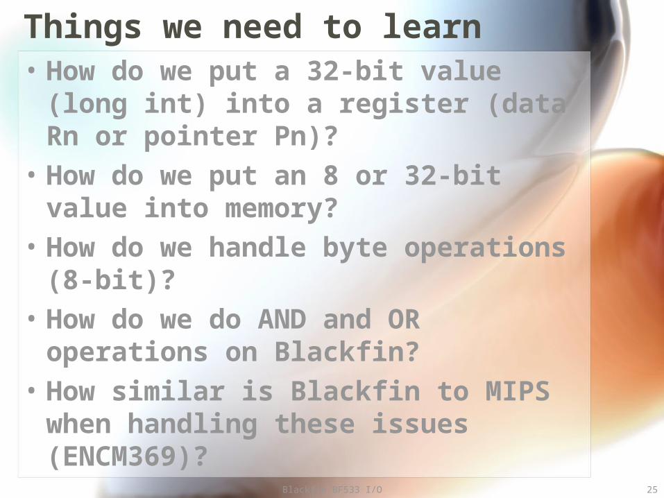
Things we need to learn• How do we put a 32-bit value (long
int) into a register (data Rn or pointer Pn)?
• How do we put an 8 or 32-bit value into memory?
• How do we handle byte operations (8-bit)?
• How do we do AND and OR operations on Blackfin?
• How similar is Blackfin to MIPS when handling these issues (ENCM369)?
Blackfin BF533 I/O 25
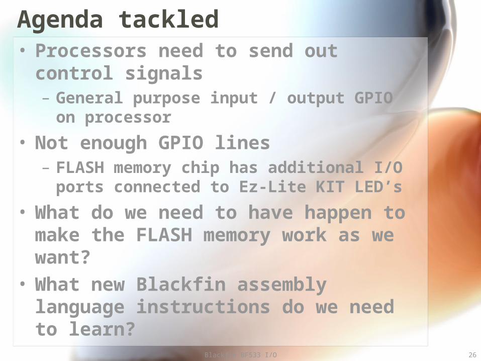
Agenda tackled• Processors need to send out control
signals– General purpose input / output GPIO on
processor
• Not enough GPIO lines– FLASH memory chip has additional I/O ports
connected to Ez-Lite KIT LED’s
• What do we need to have happen to make the FLASH memory work as we want?
• What new Blackfin assembly language instructions do we need to learn?
Blackfin BF533 I/O 26


![CRUDE OIL PRETREATMENT (DESALTING) Typical Configuration ... · Typical Configuration Atmospheric Column w/o Preflash[1,2] Fig:2.1 Typical Configuration Atmospheric Column w/o Preflash](https://img.pdfslide.us/doc/110x75/5e1a6d4c988da21e3c49a22a/crude-oil-pretreatment-desalting-typical-configuration-typical-configuration.jpg)