Embed Size (px)
Citation preview

Getmynotes.com
Getmynotes.com
Class I year, 02 sem (CSE)
Subject Code CS6201
Subject Digital Principles & System Design
Prepared By S.Seedhanadevi
Lesson Plan for Introduction to memory and programmable logic
Time: 45 Minutes
Lesson. No Unit V-Lesson No.1/9 1.CONTENT LIST:
Introduction to memory and programmable logic
2. SKILLS ADDRESSED: x Listening
3.OBJECTIVE OF THIS LESSON PLAN: To make the students learn the concept of memory and programmable logic
device
4.OUTCOMES:
i. Learn the concept of memory
ii. Describe the basic theory of programmable logic devices. 5.LINK SHEET:
i. What is memory?
ii. Give the types of memory
iii. What is PLD? iv. What are the types of PLD? v. List the major topics covered in PLD
6. EVOCATION :(5 Minutes)
CS6201-DIGITAL PRINCIPLES AND SYSTEM DESIGN Page 1
Getmynotes.com

Getmynotes.com
6.LECTURE NOTES: (40 Minutes)
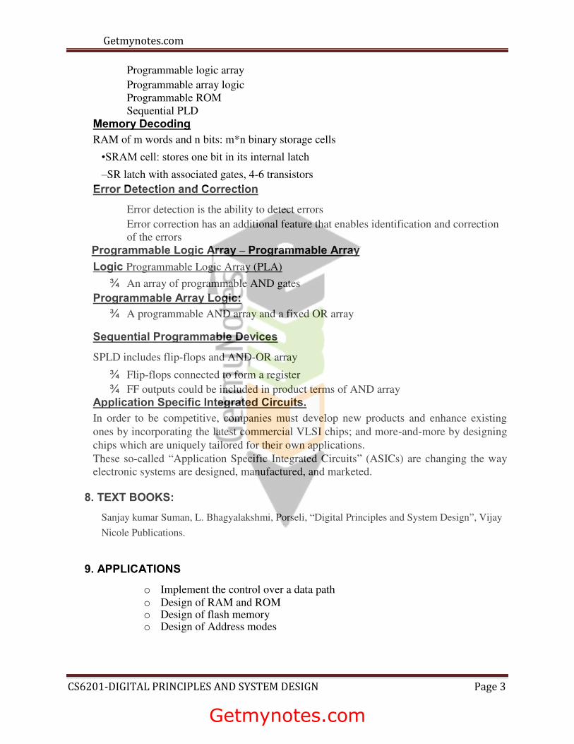
Major topics in unit V
1. Introduction to memory and programmable logic 2. RAM and ROM 3. Memory Decoding 4. Error Detection and Correction 5. Programmable Logic Array
– Programmable Array Logic
6. Sequential Programmable Devices
7. Application Specific Integrated Circuits.
8. Recap of Unit V
Introduction to memory and programmable logic
Memory unit
A collection of cells capable of storing a large quantity of binary information and
to which binary information is transferred for storage
from which information is available when needed for processing
Together with associated circuits needed to transfer information in and out of the
device • Write operation: storing new information into memory
• Read operation: transferring the stored information
Two major types: RAM & ROM
o RAM (Random-access memory): Read + Write- accept new information for
storage to be available
o ROM (Read-only memory): perform only read
Programmable Logic Devices (PLD)
¾ An integrated circuit with internal logic gates • hundreds to millions of gates interconnected through hundreds to thousands of
internal paths
¾ Connected through electronic paths that behave similar to fuse • In the original state, all the fuses are intact
¾ Programming the device • blowing those fuse along the paths that must be removed in order to obtain
particular configuration of the desired logic function.
Types of PLD
CS6201-DIGITAL PRINCIPLES AND SYSTEM DESIGN Page 2
Getmynotes.com
Getmynotes.com
Programmable logic array Programmable array logic
Programmable ROM
Sequential PLD
Memory Decoding
RAM of m words and n bits: m*n binary storage cells
•SRAM cell: stores one bit in its internal latch
–SR latch with associated gates, 4-6 transistors
Error Detection and Correction
Error detection is the ability to detect errors Error correction has an additional feature that enables identification and correction
of the errors Programmable Logic Array – Programmable Array
Logic Programmable Logic Array (PLA)
¾ An array of programmable AND gates Programmable Array Logic:
¾ A programmable AND array and a fixed OR array
Sequential Programmable Devices
SPLD includes flip-flops and AND-OR array
¾ Flip-flops connected to form a register ¾ FF outputs could be included in product terms of AND array
Application Specific Integrated Circuits.
In order to be competitive, companies must develop new products and enhance existing
ones by incorporating the latest commercial VLSI chips; and more-and-more by designing
chips which are uniquely tailored for their own applications. These so-called “Application Specific Integrated Circuits” (ASICs) are changing the way
electronic systems are designed, manufactured, and marketed.
8. TEXT BOOKS:
Sanjay kumar Suman, L. Bhagyalakshmi, Porseli, “Digital Principles and System Design”, Vijay
Nicole Publications.
9. APPLICATIONS
o Implement the control over a data path
o Design of RAM and ROM
o Design of flash memory o Design of Address modes
CS6201-DIGITAL PRINCIPLES AND SYSTEM DESIGN Page 3
Getmynotes.com

SRIVIDYA COLLEGE OF ENGINEERING AND TECHNOLOGY, VIRUDHUNAGAR
Sri Vidya College of Engineering and Technology
Department of Information Technology
Class I year, 02 sem (CSE)
Subject Code CS6201
Subject Digital Principles & System Design
Prepared By S.Seedhanadevi
Lesson Plan for RAM and ROM
Time: 45 Minutes
Lesson. No Unit V-Lesson No.2/9
1.CONTENT LIST:
RAM and ROM 2. SKILLS ADDRESSED:
x Understanding x Remembering
3.OBJECTIVE OF THIS LESSON PLAN:
To make the students understand the basic concept of RAM and ROM
4.OUTCOMES:
i. Explain concept of RAM
ii. Deduce the basic concept of ROM
5.LINK SHEET:
i. What is RAM? ii. Give the types of RAM memory.
iii. What is ROM? iv. What are the types of ROM memory?
6. EVOCATION :(5 Minutes)
CS6201-DIGITAL PRINCIPLES AND SYSTEM DESIGN Page 4
Getmynotes.com

SRIVIDYA COLLEGE OF ENGINEERING AND TECHNOLOGY, VIRUDHUNAGAR
6.LECTURE NOTES: (40 Minutes)
RAM
A memory unit stores binary information in groups of bits – 1 byte = 8 bits
– 16-bit word = 2 bytes, 32-bit word = 4 bytes
Interface
– n data input and output lines
– k address selection lines
– control lines specifying the direction of
transfer Addressing
– each word is assigned to an address
– k-bit address: 0 to 2k – 1 word
– size: K(kilo)=210, M(mega)=220, G(giga)=230
– A decoder accepts an address and opens the paths needed to selection the word
specified
CS6201-DIGITAL PRINCIPLES AND SYSTEM DESIGN Page 5
Getmynotes.com

SRIVIDYA COLLEGE OF ENGINEERING AND TECHNOLOGY, VIRUDHUNAGAR
`Example: 1K words of 16 bits
CS6201-DIGITAL PRINCIPLES AND SYSTEM DESIGN Page 6
Getmynotes.com

SRIVIDYA COLLEGE OF ENGINEERING AND TECHNOLOGY, VIRUDHUNAGAR
Write and Read Operations •Steps of Write operation
–Apply the binary address to the address lines
–Apply the data bits to the data input lines
–Activate the write input
•Steps of Read operation
–Apply the binary address to the address lines
–Activate the read input
• Two ways of control inputs: –separate read and write inputs
–memory enable (chip select) + Read/write (operation select)
• widely used in commercial or multi-chip memory components
Timing Waveforms of Memory
CS6201-DIGITAL PRINCIPLES AND SYSTEM DESIGN Page 7
Getmynotes.com

SRIVIDYA COLLEGE OF ENGINEERING AND TECHNOLOGY, VIRUDHUNAGAR
Memory operation control: usually controlled by external devices such as CPU –CPU provides memory control signals to synchronize its internal
clocked operations with memory operations
–CPU also provides the address for the
memory Memory operation times
–access time: time to select a word and read it
–cycle time: time to complete a write operation
Both must be within a time equal to a fixed number of CPU clock cycles
Types of Memories
Random vs. sequential –Random-Access Memory: each word is accessible
separately •equal access time Sequential-Access Memory: information stored is not immediately accessible
but only at certain intervals of time
•magnetic disk or tape
•access time is variable
•Static vs. dynamic
CS6201-DIGITAL PRINCIPLES AND SYSTEM DESIGN Page 8
Getmynotes.com

SRIVIDYA COLLEGE OF ENGINEERING AND TECHNOLOGY, VIRUDHUNAGAR
SRAM: consists essentially of internal latches and remains valid as long as power
is applied to the unit
DRAM: in the form of electric charges on capacitors which are provided inside
the chip by MOS transistors
ROM:
¾ Permanent binary information is stored –pattern is specified by the designer
–stays even when power is turned off and on again
¾ Pins
–k address inputs and n data outputs
–no data inputs since it doses not have a write operation
–one or more enable inputs
Example: 32x8 ROM
• A 2kxn ROM has an internal k x2k decoder and n OR • 32 words of 8 bits each
– 32*8=256 programmable internal connections
– 5 inputs decoded into 32 distinct outputs by 5x32 decoder
–Each of 8 OR gates have 32 inputs
CS6201-DIGITAL PRINCIPLES AND SYSTEM DESIGN Page 9
Getmynotes.com

SRIVIDYA COLLEGE OF ENGINEERING AND TECHNOLOGY, VIRUDHUNAGAR
Types of ROM
4 methods to program ROM paths
• Mask programming ROM – customized and filled out the truth table by customer and masked
by manufacturers during last fabrication process – costly; economical only if large quantities
• PROM: Programmable ROM –PROM units contain all the fuses intact initially
– Fuses are blown by application of a high-voltage pulse to the device through
a -special pin by special instruments called PROM programmers
–Written/programmed once; irreversible
• EPROM: erasable PROM – floating gates served as programmed connections
–When placed under ultraviolet light, short wave radiation discharges thecgates
and makes the EPROM returns to its initial state
– reprogrammable after erasure
• EEPROM: electrically-erasable PROM – erasable with an electrical signal instead of ultraviolet light
– longer time is needed to write
– flash ROM: limited times of write operations
8. TEXT BOOKS:
Sanjay kumar Suman, L. Bhagyalakshmi, Porseli, “Digital Principles and System Design”,
Vijay Nicole Publications.
9. APPLICATIONS
ROM - Read Only Memory: This is like the Operating system, the things the
computer needs and cannot be altered RAM - Random Access Memory: I think this is for temporary storage,
which is deleted
CS6201-DIGITAL PRINCIPLES AND SYSTEM DESIGN Page 10
Getmynotes.com

SRIVIDYA COLLEGE OF ENGINEERING AND TECHNOLOGY, VIRUDHUNAGAR
Sri Vidya College of Engineering and Technology
Department of Information Technology
Class I year, 02 sem (CSE)
Subject Code CS6201
Subject Digital Principles & System Design
Prepared By S.Seedhanadevi
Lesson Plan for Memory Decoding
Time: 45 Minutes
Lesson. No Unit V-Lesson No.3/9
1.CONTENT LIST:
Memory Decoding 2. SKILLS ADDRESSED:
x Learning x Remembering
3.OBJECTIVE OF THIS LESSON PLAN:
To make the students understand the concept of memory decoding
4.OUTCOMES:
i. Explain concept of memory decoding
ii. Deduce the basic concept of address multiplexing
5.LINK SHEET:
i. What is memory decoding? ii. Construct memory cell.
iii. What is coincident decoding? iv. Explain address multiplexing?
6. EVOCATION :(5 Minutes)
CS6201-DIGITAL PRINCIPLES AND SYSTEM DESIGN Page 11
Getmynotes.com

SRIVIDYA COLLEGE OF ENGINEERING AND TECHNOLOGY, VIRUDHUNAGAR
6.LECTURE NOTES: (40 Minutes)
Memory decoding
¾ RAM of m words and n bits: m*n binary storage cells •SRAM cell: stores one bit in its internal latch
¾ SR latch with associated gates, 4-6 transistors
Example: capacity of 16 bits in 4 words of 4 bits each •2x4 decoder:select one of the 4 words •enabled with the Memory enable signal. •Memory with 2k words of n bits: k address lines go into a kx2k decoder.
CS6201-DIGITAL PRINCIPLES AND SYSTEM DESIGN Page 12
Getmynotes.com

SRIVIDYA COLLEGE OF ENGINEERING AND TECHNOLOGY, VIRUDHUNAGAR
Coincident Decoding
•Decoder complexity: a decoder with k inputs and 2k outputs requires 2k AND gates
with k inputs per gate
•2-dimensional decoding: arrange cells in a square array
•2 k/2-input decoders instead of 1 k-input decoder one for row selection and the other
for column selection
•1K-word memory –a single 10x1,024 decoder: 1,024 10- input AND gates –two
5x32 decoders: 64 5-input AND gates
CS6201-DIGITAL PRINCIPLES AND SYSTEM DESIGN Page 13
Getmynotes.com

SRIVIDYA COLLEGE OF ENGINEERING AND TECHNOLOGY, VIRUDHUNAGAR
Address Multiplexing
•DRAM: large capacity requires large address decoding –Simpler cell structure
•DRAM: a MOS transistor and a capacitor per cell
•SRAM: 6 transistors –Higher density: 4 times the density of SRAM
•larger capacity
Lower cost per bit: 3-4 times less than SRAM
•Lower power requirement–Preferred technology for large memories
•64K (=216) bits and 256M(=228) bits may need 16 and 28 address inputs
•Address multiplexing: use a small set of address input pins to accommodate the address
components–A full address is applied in multiple parts at different times •i.e. two-
dimensional array: row address first and column address second
•same set of pins is used for both parts
Advantage: reducing the number of pins for larger memory
Example: 64K-word memory
• 256 rows x 256 columns for 28x28=216=64K words
• Address strobes: enabling row and column address into their respective registers (no Memory enable)
•a single data input line
CS6201-DIGITAL PRINCIPLES AND SYSTEM DESIGN Page 14
Getmynotes.com

SRIVIDYA COLLEGE OF ENGINEERING AND TECHNOLOGY, VIRUDHUNAGAR
•a single data output line
•a Read/Write control
•two address strobes–RAS: enable 8-bit row register by level 0–CAS: enable 8-bit column
register by level 0.
8. TEXT BOOKS:
Sanjay kumar Suman, L. Bhagyalakshmi, Porseli, “Digital Principles and System
Design”, Vijay Nicole Publications.
9. APPLICATIONS
o Memory decoders are most often used in more complex digital systems to access
a particular memory location based on an "address" produced by a computing
device.
o To prevent the data being "read" from each memory chip at the same time, each memory chip is selected individually one at time and this process is known as Address Decoding.
Sri Vidya College of Engineering and Technology
Department of Information Technology
Class I year, 02 sem (CSE)
Subject Code CS6201
CS6201-DIGITAL PRINCIPLES AND SYSTEM DESIGN Page 15
Getmynotes.com

SRIVIDYA COLLEGE OF ENGINEERING AND TECHNOLOGY, VIRUDHUNAGAR
Subject Digital Principles & System Design
Prepared By S.Seedhanadevi
Lesson Plan for Error Detection and Correction
Time: 45 Minutes
Lesson. No Unit V-Lesson No.4/9
1.CONTENT LIST:
Error Detection and Correction 2. SKILLS ADDRESSED:
x Learning x Remembering x Applying
3.OBJECTIVE OF THIS LESSON PLAN:
To make the students understand the concept of error detection and
correction 4.OUTCOMES:
i. Explain concept of error detection
ii. Deduce the basic concept of error correction
5.LINK SHEET:
i. What is error detection? ii. How error is corrected?
iii. Explain the parity bits and their significance in detecting and correcting error.
iv. Deduce the significance of hamming codes in error correction and detection.
6. EVOCATION :(5 Minutes)
6.LECTURE NOTES: (40 Minutes)
Error Detection and Correction
o Error detection is the ability to detect errors Error correction has an additional feature that enables identification and correction of the errors
o Error detection always pecedes error correction Both can be achieved by having extra/redundant/check bits in addition to data deduce that there is an
CS6201-DIGITAL PRINCIPLES AND SYSTEM DESIGN Page 16
Getmynotes.com

SRIVIDYA COLLEGE OF ENGINEERING AND TECHNOLOGY, VIRUDHUNAGAR
o error
o Original Data is encoded with the redundant bit(s) o New data formed is known as code word
The simplest and oldest error detection method
Parity bits o A binary digit called parity is used to indicate whether the number of bits with “1”
in a given set of bits is even or odd
o The parity bit is then appended to original data
o Usually used to detect transmission error o Sender adds the parity bit to existing data bits before transmission o Receiver checks for the expected parity, If wrong parity found, the received data
is discarded and retransmission is requested.
Parity type: Even
o Forced an even number of one’s on total data sent o 000 0001 1000 0001 o 000 0011 0001 0001
o Generating even parity bit is just an XOR function o Data Received Examples:
0111 1111 - incorrect
1000 0000 - incorrect
1000 0001 - valid o Note that error could be in data or parity
o Not entirely fool proof
Parity type: Odd
Forced an odd number of one’s 000 0001 0 000 0001
000 0011 1 000 0011
Odd parity is generated using a XNOR function
Hamming Distance and Error Detection
o Hamming Distance = of bit positions in which 2 code words differ o E.g. 10001001 and 10110001 have distance of 3
o If distance is d, then d-single bit errors are required to convert any one valid code into another
o Implying that this error would not be detected o Could detect 1-bit error as 4 code words had hamming distance = 2 o But could not detect 2-bit error o In general, to detect k-single bit error, minimum hamming distance D(min) = k
+ 1
o If there is a larger hamming distance between valid code words o Then we may be able to determine which valid codeword was o intended o Suppose a code needs just 2 different values, and we use:
CS6201-DIGITAL PRINCIPLES AND SYSTEM DESIGN Page 17
Getmynotes.com
SRIVIDYA COLLEGE OF ENGINEERING AND TECHNOLOGY, VIRUDHUNAGAR
o One valid value = 0000 0000 and the other = 1111 1111Then distance between
these is 8
o Suppose we got 2 bit changes so that:0000 0000 became 0011 0000
o The greater the distance between valid code words, the easier it is to figure what the correct codeword was Requires additional redundant bits (> 1 parity bit) to chose code words that are far apart
o D(min) = 2k + 1 is required for correcting k-errors
o Hamming Code is type of Error Correcting Code (ECC) o Provides error detection and correction mechanism o Adopt parity concept, but have more than one parity bit o In general hamming code is code word of n bits with m data bits and r parity (or
check bits) i.e. n = m + r o Can detect D(min) – 1 errors
o Can correct errors o Hence to correct k errors, need D(min) = 2k + 1
o Need a least a distance of 3 to correct a single bit error. Determining of Parity bits for single-bit correction
o Hamming Code for single-bit error correction is the most commonly used Experiments (IBM study) show 98% time there are single-bit errors.
o Need determine r for m-data bits that provides code words of n-bits that has single-bit correction capabilities.
Hamming Code: Determining Parity bits for single-bit correction
o Because n = m + r, we can rewrite the inequality as: (m + r + 1) × 2 m ≤ 2 m + r or (m + r + 1) ≤ 2 r
o This inequality gives us a lower limit on the number of parity bits that we need in our code words
o Example: Suppose we have data words of length m = 4, (4 + r + 1) ≤ 2 r
o Implies that r must be greater than or equal to 3 o To build a code with 4-bit data words that will correct single-bit errors, we must
add 3 check bits.
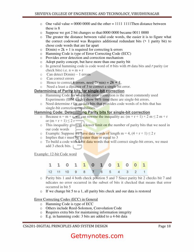
Example: 12-bit Code word
o Parity bits 1 and 4 both check position 5 and 7 Since parity bit 2 checks bit 7 and
ndicates no error occurred in the subset of bits it checked that means that error
occurred in bit 5
o If we change bit 5 to a 1, all parity bits check and our data is restored
Error Correcting Codes (ECC) in General o Hamming Code is type of ECC o Others include Reed-Solomon, Convolution Code o Requires extra bits for maintaining information integrity o E.g. in hamming code: 3 bits are added to a 4-bit data
CS6201-DIGITAL PRINCIPLES AND SYSTEM DESIGN Page 18
Getmynotes.com

SRIVIDYA COLLEGE OF ENGINEERING AND TECHNOLOGY, VIRUDHUNAGAR
o The overhead of extra bits does pay off
o Single-bit correction often costs less than sending the entire data twice o If the storage is the only source of data (e.g. disk or DRAM) then we want a error-
correction to avoid crashing of programs
8. TEXT BOOKS:
Sanjay kumar Suman, L. Bhagyalakshmi, Porseli, “Digital Principles and System Design”,
Vijay Nicole Publications. 9. APPLICATIONS
o Error detection and correction or error control is techniques that enable reliable
delivery of digital data over unreliable communication channels.
o Many communication channels are subject to channel noise, and thus errors may be introduced during transmission from the source to a receiver.
o Error detection techniques allow detecting such errors, while error correction enables reconstruction of the original data.
CS6201-DIGITAL PRINCIPLES AND SYSTEM DESIGN Page 19
Getmynotes.com
SRIVIDYA COLLEGE OF ENGINEERING AND TECHNOLOGY, VIRUDHUNAGAR
Sri Vidya College of Engineering and Technology
Department of Information Technology
Class I year, 02 sem (CSE)
Subject Code CS6201
Subject Digital Principles & System Design
Prepared By S.Seedhanadevi
Lesson Plan for Programmable Logic Array– Programmable Array Logic
Time: 45 Minutes
Lesson. No Unit V-Lesson No.5/9
1.CONTENT LIST:
Programmable Logic Array– Programmable Array Logic 2. SKILLS ADDRESSED:
x Understanding x Applying
3.OBJECTIVE OF THIS LESSON PLAN:
To make the students learn the concept of PLA and PAL
4.OUTCOMES:
i. Explain concept of PLA
ii. Deduce the logic diagram of PLA
5.LINK SHEET:
i. What are combinational PLD’s ii. What is PLA
iii. Construct PLA
iv. Illustrate the concept with an example
6. EVOCATION :( 5 Minutes)
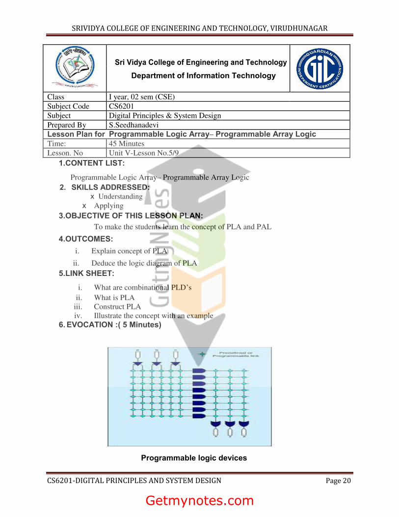
Programmable logic devices
CS6201-DIGITAL PRINCIPLES AND SYSTEM DESIGN Page 20
Getmynotes.com

SRIVIDYA COLLEGE OF ENGINEERING AND TECHNOLOGY, VIRUDHUNAGAR
6.LECTURE NOTES: (40 Minutes)
Combinational PLDs Combinational programmable logic device (PLD)
x Programmable gates divided into an AND array and an OR array x Provide an AND-OR sum of product implementation
o A fixed AND array constructed as a decoder
o A programmable OR array to implement Boolean functions in sum of minterms o A programmable AND array: to provide the product terms for Boolean functions o Both can be programmed
o Most flexible
Programmable Logic Array
CS6201-DIGITAL PRINCIPLES AND SYSTEM DESIGN Page 21
Getmynotes.com

SRIVIDYA COLLEGE OF ENGINEERING AND TECHNOLOGY, VIRUDHUNAGAR
¾ An array of programmable AND gates x Can generate any product terms of the inputs
¾ An array of programmable OR gates x Can generate the sums of the products
¾ Only the needed product terms are generated (not all) ¾ More flexible than ROM; use less circuits than ROM
¾ Size of PLA: specified by # of inputs, product terms and outputs
x n inputs, k product terms and m outputs x n buffer-inverter gates, k AND gates, m OR gates, and m XOR
gates x Typical PLA may have 16 inputs, 48 product terms and 8 outputs
¾ Designing a digital system with a PLA x Reduce the number of distinct product terms x The number of literals in a product is not important
¾ Implementing PLA x Mask programmable PLA: submit a PLA program table to the
manufacturer x Field Programmable (FPLA): by commercial hardware
programmer unit
` PLA Example 1
Example: AND/OR/XOR
F1 = AB′ + AC + A′BC′
F2 = (AC + BC) ′
Design
PLA programming table: 4 sections
1. List the product terms 2. Specify the required paths between inputs and and gates 3. Specify the paths between the and and or gates 4. Specifying the fuse map and submitted to the manufacturer
o XOR gates can invert the outputs
o Invert: connected to 1
o Not change: connected to 0
CS6201-DIGITAL PRINCIPLES AND SYSTEM DESIGN Page 22
Getmynotes.com

SRIVIDYA COLLEGE OF ENGINEERING AND TECHNOLOGY, VIRUDHUNAGAR
PLA Example 2
Implement: F1(A, B, C) = Σ (0, 1, 2, 4); F2(A, B, C) = Σ (0, 5, 6, 7)
1. Simply both the true and complement of the functions in sum of products
2. Find the combination with minimum number of product terms
F1=(AB+AC+BC)’ F2=AB+AC+A’B’C’
3. Obtain the PLA Programming table
CS6201-DIGITAL PRINCIPLES AND SYSTEM DESIGN Page 23
Getmynotes.com

SRIVIDYA COLLEGE OF ENGINEERING AND TECHNOLOGY, VIRUDHUNAGAR
8. TEXT BOOKS:
Sanjay kumar Suman, L. Bhagyalakshmi, Porseli, “Digital Principles and System
Design”, Vijay Nicole Publications.
9. APPLICATIONS
The applications of programmable array logic transform the analogue
circuits to digital circuit. PLA is used to implement the control over a datapath.
CS6201-DIGITAL PRINCIPLES AND SYSTEM DESIGN Page 24
Getmynotes.com

SRIVIDYA COLLEGE OF ENGINEERING AND TECHNOLOGY, VIRUDHUNAGAR
Sri Vidya College of Engineering and Technology
Department of Information Technology
Class I year, 02 sem (CSE)
Subject Code CS6201
Subject Digital Principles & System Design
Prepared By S.Seedhanadevi
Lesson Plan for Programmable Logic Array – Programmable Array Logic
Time: 45 Minutes
Lesson. No Unit V-Lesson No.6/9
1.CONTENT LIST:
Programmable Logic Array – Programmable Array Logic 2. SKILLS ADDRESSED:
x Learning x Understanding x Applying
3.OBJECTIVE OF THIS LESSON PLAN:
To make the students understand the concept of programmable array
logic 4.OUTCOMES:
i. Explain concept of Programmable array logic
ii. Deduce the logic diagram of PAL
5.LINK SHEET:
i. What is PAL? ii. Construct PAL.
iii. Illustrate PAL with example
6.EVOCATION :(5 Minutes)
CS6201-DIGITAL PRINCIPLES AND SYSTEM DESIGN Page 25
Getmynotes.com

SRIVIDYA COLLEGE OF ENGINEERING AND TECHNOLOGY, VIRUDHUNAGAR
7.LECTURE NOTES: (40 Minutes)
Programmable Array Logic
PAL: a programmable AND array and a fixed OR array – easier to program, but not as
flexible as PLA
x Example: PAL with 4 inputs, 4 outputs, and 3-wide AND-OR structure (Figure 7-16) x each input has a buffer-inverter gate •each output is generated by a fixed OR x gate x 4 sections of 3-wide AND-OR array – each AND gate has 10 programmable x input connections x A typical PAL may have 8 inputs, 8 outputs, and 8 sections, each consisting of an 8- x wide AND-OR array x May use two sections to implement a large Boolean function Product terms cannot be
shared x Each function is simplified itself
CS6201-DIGITAL PRINCIPLES AND SYSTEM DESIGN Page 26
Getmynotes.com

SRIVIDYA COLLEGE OF ENGINEERING AND TECHNOLOGY, VIRUDHUNAGAR
Example: PAL Implementation
•Implement the following functions
w(A,B,C,D) = Σ(2,12,13)
x(A,B,C,D) = Σ(7,8,9,10,11,12,13,14,15)
y(A,B,C,D) = Σ(0,2,3,4,5,6,7,8,10,11,15)
z(A,B,C,D) = Σ(1,2,8,12,13)
•Simplify the functions using k map
w = ABC′ + A′B′CD′
x = A + BCD
y = A′B + CD + B′D′
z = ABC′ + A′B′CD′ + AC′D′ + A′B′C′D
= w + AC′D′ + A′B′C′D
CS6201-DIGITAL PRINCIPLES AND SYSTEM DESIGN Page 27
Getmynotes.com

SRIVIDYA COLLEGE OF ENGINEERING AND TECHNOLOGY, VIRUDHUNAGAR
8. TEXT BOOKS:
Sanjay kumar Suman, L. Bhagyalakshmi, Porseli, “Digital Principles and System
Design”, Vijay Nicole Publications.
9. APPLICATIONS
Programmable array logic is used for designing the digital circuits easily.
Example large function which has several variables can easily
implemented by using programmable array logic.
These are the type of PLD's programmable logic devices.
CS6201-DIGITAL PRINCIPLES AND SYSTEM DESIGN Page 28
Getmynotes.com

SRIVIDYA COLLEGE OF ENGINEERING AND TECHNOLOGY, VIRUDHUNAGAR
Sri Vidya College of Engineering and Technology
Department of Information Technology
Class I year, 02 sem (CSE)
Subject Code CS6201
Subject Digital Principles & System Design
Prepared By S.Seedhanadevi
Lesson Plan for Sequential Programmable Devices
Time: 45 Minutes
Lesson. No Unit V-Lesson No.7/9
1.CONTENT LIST:
Sequential Programmable Devices 2. SKILLS ADDRESSED:
x Understanding x Applying
3.OBJECTIVE OF THIS LESSON PLAN:
To make the students learn the concept of
SPLD 4.OUTCOMES:
i. Explain concept of SPLD
ii. Deduce the major types of SPLD
5.LINK SHEET:
i. What is SPLD? ii. Construct SPLD
iii. List the major types of SPLD
iv. Discuss in detail the types of sequential programmable devices.
6. EVOCATION :( 5 Minutes)
Sequential Programmable devices
CS6201-DIGITAL PRINCIPLES AND SYSTEM DESIGN Page 29
Getmynotes.com
SRIVIDYA COLLEGE OF ENGINEERING AND TECHNOLOGY, VIRUDHUNAGAR
6.LECTURE NOTES: (40 Minutes)
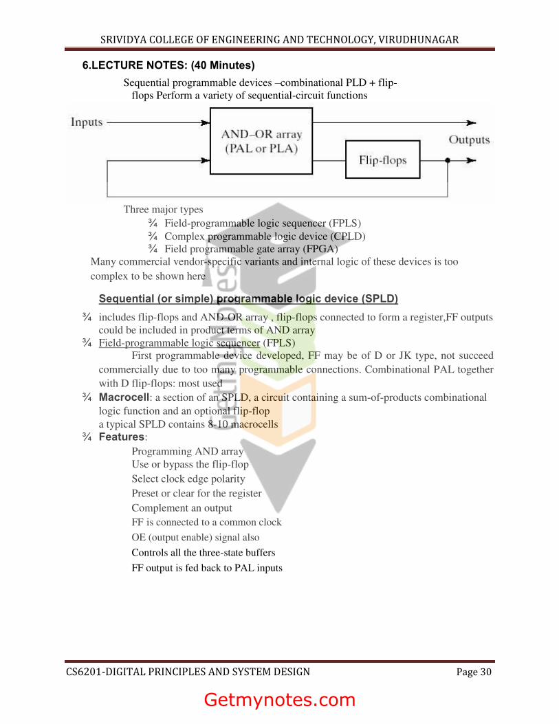
Sequential programmable devices –combinational PLD + flip-
flops Perform a variety of sequential-circuit functions
Three major types
¾ Field-programmable logic sequencer (FPLS) ¾ Complex programmable logic device (CPLD)
¾ Field programmable gate array (FPGA)
Many commercial vendor-specific variants and internal logic of these devices is too
complex to be shown here
Sequential (or simple) programmable logic device (SPLD)
¾ includes flip-flops and AND-OR array , flip-flops connected to form a register,FF outputs
could be included in product terms of AND array ¾ Field-programmable logic sequencer (FPLS)
First programmable device developed, FF may be of D or JK type, not succeed
commercially due to too many programmable connections. Combinational PAL together
with D flip-flops: most used ¾ Macrocell: a section of an SPLD, a circuit containing a sum-of-products combinational
logic function and an optional flip-flop a typical SPLD contains 8-10 macrocells
¾ Features:
Programming AND array Use or bypass the flip-flop
Select clock edge polarity
Preset or clear for the register
Complement an output
FF is connected to a common clock
OE (output enable) signal also
Controls all the three-state buffers
FF output is fed back to PAL inputs
CS6201-DIGITAL PRINCIPLES AND SYSTEM DESIGN Page 30
Getmynotes.com

SRIVIDYA COLLEGE OF ENGINEERING AND TECHNOLOGY, VIRUDHUNAGAR
CPLD - Complex Programmable Logic Device
CPLD: a collection of PLDs to be connected to each othe rthrough a programmable switch matrix
Input/output blocks provide connections to IC pins
Each I/O pin is driven by a three-state buffer and can be programmed to act as input or output
Switch matrix receives inputs from I/O block and directs it to individual microcells
Selected outputs from microcells are sent to the outputs as needed
Each PLD typically contains from 8 to 16 microcells.
FPGA – Field-Programmable Gate Array
o Gate array: basic component used in VLSI–consist of a pattern of gates fabricated in an area of silicon and repeated thousands of times
o FPGA: an array of hundreds or thousands of logic blocks – surrounded by programmable input and output blocks– connected together via programmable interconnections
CS6201-DIGITAL PRINCIPLES AND SYSTEM DESIGN Page 31
Getmynotes.com

SRIVIDYA COLLEGE OF ENGINEERING AND TECHNOLOGY, VIRUDHUNAGAR
o A logic block consists of look-up tables, multiplexers, gates, and flip-flops
o Look-up table: a truth table stored in a SRAM and providing combinational circuit functions for the logic block
o SRAM instead of ROM
o Advantage: the table can be programmed o Drawback: memory is volatile, reload/reprogram required after power on
again
o Complexity
PALs, PLAs = 10 - 100 Gate Equivalents
FPGAs = 100 - 1000(s) of Gate Equivalents
8. TEXT BOOKS:
Sanjay kumar Suman, L. Bhagyalakshmi, Porseli, “Digital Principles and System
Design”, Vijay Nicole Publications.
9. APPLICATIONS
They are used in ¾ DVD Players, ¾ TV Sets
¾ Controller Circuits
¾ Internet Routers
¾ Network Switches
CS6201-DIGITAL PRINCIPLES AND SYSTEM DESIGN Page 32
Getmynotes.com

SRIVIDYA COLLEGE OF ENGINEERING AND TECHNOLOGY, VIRUDHUNAGAR
Sri Vidya College of Engineering and Technology
Department of Information Technology
Class I year, 02 sem (CSE)
Subject Code CS6201
Subject Digital Principles & System Design
Prepared By S.Seedhanadevi
Lesson Plan for Application Specific Integrated Circuits.
Time: 45 Minutes
Lesson. No Unit V-Lesson No.8/9
7.CONTENT LIST:
Application specific integrated circuits 8. SKILLS ADDRESSED:
x Understanding x Analyzing
9.OBJECTIVE OF THIS LESSON PLAN:
To make the students learn the concept of ASIC
10. OUTCOMES:
iii. Explain concept of ASIC
iv. Describe the overview of ASIC design options 11. LINK SHEET:
vi. What is ASIC?
vii. Construct the hierarchy of ASIC
viii. Discuss in detail the design options of ASIC.
ix. Explain the fabrication of ASIC
6. EVOCATION :( 5 Minutes)
CS6201-DIGITAL PRINCIPLES AND SYSTEM DESIGN Page 33
Getmynotes.com

SRIVIDYA COLLEGE OF ENGINEERING AND TECHNOLOGY, VIRUDHUNAGAR
12. LECTURE NOTES: (40 Minutes)
Application specific integrated circuits
Advancements in Very Large Scale Integration (VLSI) technology have brought chips with
millions of transistors into our laboratories, offices, and homes. In order to be competitive, companies must develop new products and enhance existing
ones by incorporating the latest commercial VLSI chips; and more-and-more by designing
chips which are uniquely tailored for their own applications.
These so-called “Application Specific Integrated Circuits” (ASICs) are changing the way
electronic systems are designed, manufactured, and marketed.
Overview of ASIC Design Options
This section introduces the range of options and styles available for integrated
circuit design. Although the bulk of this chapter will focus on the programmable logic
design style, this section places programmable logic in context alongside the alternate
design techniques.
The following sections are loosely organized in order of decreasing design investment
(non-recurring engineering costs) and corresponding maximum chip complexity.
Full Custom Design
In the classic full custom design style, each primitive logic function or transistor is
Manually designed and optimized. This results in the most compact chip design with the
highest possible speed and lowest power dissipation.
However, the initial investment or Non-Recurring Engineering (NRE) cost is highest
compared to all other design styles.
The designer must manipulate the individual geometric shapes which represent the
features of each transistor on the chip; hence the often applied term for full custom
design: “polygon pushing”.
A relatively simple 3000 gate design might require the handling of 300,000 rectangles per
chip.
CS6201-DIGITAL PRINCIPLES AND SYSTEM DESIGN Page 34
Getmynotes.com

SRIVIDYA COLLEGE OF ENGINEERING AND TECHNOLOGY, VIRUDHUNAGAR
Standard Cell Design
In the standard cell design methodology, pre-defined logic and function blocks are made
available to the designer in a cell library. Typical libraries begin with gate level
primitives such
as AND, OR, NAND, NOR, XOR, Inverters, flip-flops, registers, and the like. Libraries
generally include more complex functions such as adders, multiplexers, decoders, ALUs,
shifters, and memory (RAM, ROM, FIFOs, etc.).
In some cases, the standard cell library may include complex functions such as
multipliers, dividers, microcontrollers, microprocessors, and microprocessor support
functions (parallel port, serial port, DMA controller, event timers, real-time clock, etc.).
Gate Array Design
Full custom and standard cell design methodologies require custom chip fabrication using
a complete set of unique masks which define the semiconductor processing of the design.
Thus, both the NRE cost for the mask set and the design turn-around time through the
foundry is quite high.
As an alternative, a chip design can be created using a custom interconnection pattern on
an array of uncommitted logic gates (i.e. a gate array).
Wafers of chips containing the uncommitted logic gate arrays can be pre-fabricated up to
the point of the final metalization steps which create the logic personalization.
Compared to standard cell or full custom designs, the design turnaround time and cost are
reduced because only the top level interconnect and contact mask steps (2-5 masks) need
to be applied.
Field Programmable Logic
A field programmable logic device is a chip whose final logic structure is
directly configured by the end user.
By eliminating the need to cycle through an integrated circuit
production facility, both time to market and financial risk can be substantially reduced.
The two major classes of field programmable logic, Programmable Logic Devices
(PLDs) and Field Programmable Gate Arrays (FPGAs), have emerged as cost effective
ASIC solutions because they provide low-cost prototypes with nearly instant
manufacturing”.
This class of device consists of an array of uncommitted logic elements whose
interconnect structure and/or logic structure can be personalized on-site according to the
user’s specification.
CS6201-DIGITAL PRINCIPLES AND SYSTEM DESIGN Page 35
Getmynotes.com

SRIVIDYA COLLEGE OF ENGINEERING AND TECHNOLOGY, VIRUDHUNAGAR
ASIC Fabrication Technologies
This treatment is not intended as an in-depth tutorial on semiconductor devices and fabrication,
but rather to identify the minimum information necessary to enable designers to make intelligent
technology choices. In order to appreciate the capabilities and limitations of a particular
technology, the ASIC user or designer must know the characteristics of the pertinent fabrication
technology. CMOS is currently the dominant ASIC fabrication technology due to its many advantages
including cost, performance, density, and manufacturing / designer experience. Referring back
to the Gate Array and FPGA entries in Table 1, the prediction is that CMOS will continue to
gain market share over bipolar technologies. Although designers typically lump ASIC designs into two groups, CMOS and “other”
technologies, this section attempts to take broader view of the technology alternatives.
Bipolar, BiCMOS, and GaAs ASICs each have unique advantages for many high performance
applications. Figure 3 presents taxonomy of available semiconductor process technologies for ASICs. At the topmost level, the tree splits into silicon and gallium arsenide (GaAs) technologies. GaAs
9 has been slowly expanding from its historical markets in the military and aerospace fields; and
may be ready to expand into the mainstream digital IC market.
CS6201-DIGITAL PRINCIPLES AND SYSTEM DESIGN Page 36
Getmynotes.com

SRIVIDYA COLLEGE OF ENGINEERING AND TECHNOLOGY, VIRUDHUNAGAR
The most dominant commercially available GaAs technologies are Direct Coupled FET Logic (DCFL) and Source-Coupled FET Logic (SCFL). DCFL is similar in design to
NMOS and because of its low transistor count circuits provides higher gate-count chips. It’s
speed is comparable to bipolar Emitter Coupled Logic (ECL) with a 60% reduction in
power dissipation. SCFL has significantly higher speed than DCFL, with a correspondingly higher power
dissipation. Other common GaAs technologies include Buffered FET Logic (BFL) and
Bipolar Integrated Shottkey Logic (BSL).
The most important class of unipolar devices for ASICs are the Metal-Oxide
Semiconductor (MOS) devices used in the PMOS, NMOS, and CMOS processes. While
other unipolar technologies exist, such as the Metal-Nitride Oxide Semiconductor (MNOS)
process used in nonvolatile memories, they do not represent a significant part of the ASIC
market. Although universally used today, the acronym MOS is an outdated term. Metal
refers to the gate layer, Oxide refers to the silicon dioxide insulator, and Semiconductor to
the channel being controlled by the gate. MOS processes today make almost exclusive use of
polysilicon rather than metal for the gate material.
Finally, BiCMOS is a relatively recent technology introduction which incorporates both
Bipolar and CMOS devices on the same chip. Typically, most of the logic in a BiCMOS
ASIC is CMOS, while the bipolar devices are used for on-chip and off-chip drivers. The
advantage of the bipolar drivers is that they are capable of driving much higher loads without
sacrificing speed. Compared to CMOS, BiCMOS is significantly faster, but chip cost can be
two or three times higher
8. TEXT BOOKS:
Sanjay kumar Suman, L. Bhagyalakshmi, Porseli, “Digital Principles and System
Design”, Vijay Nicole Publications.
9. APPLICATIONS
High density
Low power dissipation compared to other processing technologies in use today.
Low-voltage applications
CS6201-DIGITAL PRINCIPLES AND SYSTEM DESIGN Page 37
Getmynotes.com