Embed Size (px)
Citation preview

1
GESTURE RECOGNITION USING FPGA
Final Year Project Evaluation 2010 – 2011
1 5 /0 3 /2 0 1 1

2
Guide: Jagadeesh Kumar P Roll no Name
ECU07201 Aarathy Udayabhanu
ECU07214 Franklin Geo Francis
ECU07225 Namsheer K
ECU07228 Nithin Sarath
ECU07234 Rizwana A •
1 5 /0 3 /2 0 1 1Gesture Recognition using FPGA

3
At a Glance….
• Introduction• Basic Overview• Video Decoder • Video Receiver• Edge Detection & Feature Extraction• VGA Display• Project Status• Future Scope• References
• 1 5 /0 3 /2 0 1 1Ge s tu re Re cog n it ion u s in g FPGA

4
Gestures Tell A Lot!!
•Gesture Recognition using FPGA
1 5 /0 3 /2 0 1 1

5
AIM
• Implement a system to recognize a Gesture
•
•Control a Windows Interface based on this Gesture
1 5 /0 3 /2 0 1 1Ge s tu re Re cog n it ion u s in g FPGA

6
Block Diagram
CAMERA
VDEC Ca rd
LINE FIELDDECODER
MEMORY
EDGE DETECTION &FEATURE EXTRACTION
MEMORYCONTROLLER
VGA CONTROLLER
MONITOR
I2C MASTERCONTROLLER
FPGA

7
Video Decoder
•Why??qCamera outputs are normally analog
qA decoder is used to digitize the analog video input
qDigitizes the (NTSC/PAL/SECAM) 4:2:2 YCbCr
format
15/03/2011Gesture Recognition using FPGA
8
Digilent Video Decoder Board
FeaturesqInputs: Component,
Composite and S Video I2C Compatible Serial Bus
qHigh Speed Hirose FX2 Connector
qOutputs : 8/16 bit YCbCr ,HS,VS and Field Signals
qProgrammable Controls : Hue, Brightness, Saturation, Contrast
q
Carrier for the Analog Devices ADV7183B Video Decoder Chip
15/03/2011

9
SDV Multiformat SDTV Video Decoder
ADV7183B
•
• High quality ,single chip ,multiformat video decoder
• i/p(Composite, S video, Component video) o/p Digital ITU-R BT.656
•• Front End:
qThree 10 Bit ADC ‘s
q12 channel input Mux
qCurrent and Voltage Clamps
•• Two wire Serial MPU
interface : I2C Compatible
•
15/03/2011Gesture Recognition using FPGA

10
Features ADV7183B is fabricated in a 3.3 V CMOS process
Automatic NTSC/PAL/SECAM identification
Digital output formats (8-bit or 16-bit)
ITU-R BT.656 YCrCb 4:2:2 output + HS, VS, and FIELD
Integrated analog muxing section that allows more than one
source of video signal to be connected to the decoder
Programmable video controls
Peak white/hue/brightness/saturation/contrast
Integrated on-chip video timing generator
Power-down mode
15/03/2011Gesture Recognition using FPGA

11
I2C Interface
• Two inputs: Serial Data (SDA) & Serial Clock(SCK)
:Carries information b/w ADV7183B & FPGA• Each device has unique address & operates as
either slave or master•
• Master : Initiates data transfer (FPGA) : Generates Clock Signals•
• Slave : Receives data sent by Master (ADV 7183B) : Generates ACK bit 15/03/2011Gesture Recognition using FPGA

12
START High to Low on SDA High in SCL8 bits shifted: Address (7 bit ) + R/W Peripheral that recognizes the transmitted address pulls Data line Low(the
9th clock pulse) Acknowledge bit. STOP Low to High on SDA
High on SCL
15/03/2011Gesture Recognition using FPGA

13
I2C Communication in ADV7183B
• ADV 7183B has two slave address for Read and Write
•
•
•
•
•
• The data sent on the SDA line to the ADV7183 includes
q7 bit slave address + 1 bit (R/W)– to identify the slave
q8 bit register address - to select one of the 249 sub addresses, thus enable access to the internal registers
q8 bit data – the data to be stored in the selected register
1 5 /0 3 /2 0 1 1Ge s tu re Re cog n it ion u s in g FPGA
14
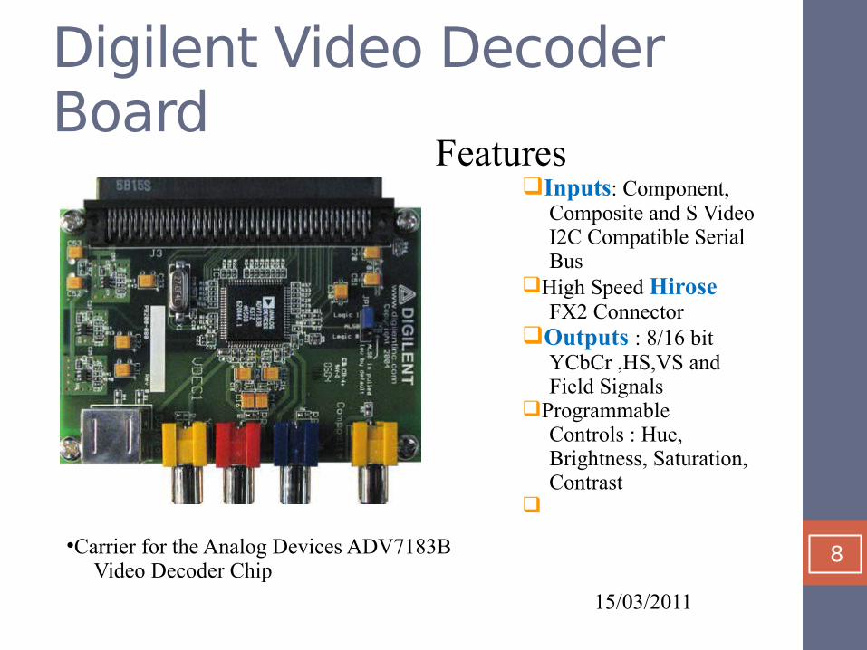
Bus Communication
START condition
Address of ADV 7183B SDA Line
ACK bit occurs
Sub address of the register
ACK bit occurs
Data sent from ADV 7183B FPGA
ACK bit occurs
STOP condition 15/03/2011

15
VHDL Implementation
VDEC CARDwith
ADV7183B
I2C MASTER CONTROLLER implemented on FPGA
15/03/2011Gesture Recognition using FPGA

16
15/03/2011

17
Video Receiver
Line Field Decoder(Obtain the Luminance (Y) from the Video Stream)
Memory Controller(R/W)Memory(BRAM)
15/03/2011Gesture Recognition using FPGA

18
ITU-R BT 656 4:2:2 YCrCb Video Format
Parallel Data Format for NTSC video frames
15/03/2011Gesture Recognition using FPGA

19
X Y Status Word
The XY status word an SAV / EAV sequence defined as:
F = 0 for odd fields; F = 1 for even fieldsV = 1 during vertical blankingH = 0 at SAV, H = 1 at EAVP3-P0 = protection bitsP3 = V xor HP2 = F xor HP1 = F xor VP0 = F xor V xor H
15/03/2011

20
15/03/2011

21
Memory
• Virtex II P•
• 18Kb blocks of memory
• Generated Using Core Generator•
• Stores 640x244 Pixels
Dis t rib u te d RAM
Block RAM
1 5 /0 3 /2 0 1 1Ge s tu re Re cog n it ion u s in g FPGA

22

23

24
Memory Controller • Controls Read & Write Operation
qWriting§ Checks for EAV and SAV Code§ Stores only 244 lines§ Next “WRITE” occurs only after
entire memory is Read
qReading § After entire WRITE operation
is over ,data is Read § o/p Passed over to the Edge
Detection Module§ Has to read data in 3x3 Matrix form
1 5 /0 3 /2 0 1 1Ge s tu re Re cog n it ion u s in g FPGA

25
6 4 0 p ixe ls
2 4 4 p ixe ls
3 x3 Ma t rix Form a t
1 5 /0 3 /2 0 1 1Ge s tu re Re cog n it ion u s in g FPGA

26
Implementation
• In VHDL
1 5 /0 3 /2 0 1 1Ge s tu re Re cog n it ion u s in g FPGA

27
EDGE DETECTION
• Fundamental step in image processing
• Images contain redundant data
• Most important data Edges
• Represents regions with strong image
contrasts
• Filters out useless information
1 5 /0 3 /2 0 1 1Ge s tu re Re cog n it ion u s in g FPGA

28
Gradient Method• Edge Detection
Laplacian •
• Our project Gradient MethodqRobert Cross qPrewittqCanny qSobel
1 5 /0 3 /2 0 1 1Ge s tu re Re cog n it ion u s in g FPGA

29
Sobel Operator
• Performs a 2-D spatial gradient measurement on an image
•
15/03/2011

30
• Two 3x3 Convolution Masks q Gradient in x –direction G x
qGradient in y-direction G y
• ‘A’ Input Image
Ma g n itu d e of th e g ra d ie n t is ca lcu la te d u s in g th e e q u a t ion
15/03/2011

31
Implementation
15/03/2011Gesture Recognition using FPGA

32
MATLAB Outputs
Input Image
15/03/2011

33 Horizontal Edge Vertical Edge
15/03/2011Gesture Recognition using FPGA

34Horizontal +Vertical Edges Edge Detection Output
15/03/2011Gesture Recognition using FPGA

35
VHDL Implementation
• Edge detection for a 3x3 input pixels was
implemented in VHDL
• Simulated using ISE 10.1
• Input for the operation was read from BRAM
• “Non-Restoring Square root Algorithm” was
written in VHDL package for the calculation of
the absolute value
• Based on the threshold value ,a ‘1’ or ‘0’ was
assigned15/03/2011Gesture Recognition using FPGA

36
Testing
15/03/2011Gesture Recognition using FPGA

37
Simulation Output
15/03/2011Gesture Recognition using FPGA

38
Simulation Output
15/03/2011Gesture Recognition using FPGA

39
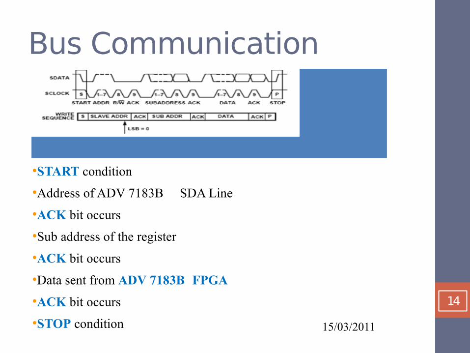
Feature Vectors
• Mathematical Description of Image
• Feature vectors:-• Area• Perimeter• Length and Width of fingers• Moment of Area• Centroid
• Compare the obtained values of feature vector with the
reference values
1 5 /0 3 /2 0 1 1Ge s tu re Re cog n it ion u s in g FPGA
40
FEATURE VECTORS
•
• Perimeter :No. of white pixels in the boundary
• Area :No. of black pixels inside the white contour
• Length :Difference b/w top and bottom most white pixels
•
• Width :Difference b/w left and right white pixels
1 5 /0 3 /2 0 1 1Ge s tu re Re cog n it ion u s in g FPGA

41
In a nutshell ….
Im a g e (Y va lu e s from BRAM)
Ma g n itu d e Com p u te d
Fe a tu re Ve cto rs Ca lcu la te d
Ed g e Ob ta in e d
Gx & Gy Computed
Thresholding Performed
Gestures recognized
A
A
15/03/2011

42
VGA Display640
480
15/03/2011Gesture Recognition using FPGA

43
15/03/2011Gesture Recognition using FPGA

44
Timing Diagram
15/03/2011Gesture Recognition using FPGA

45
Video Parameters
• HSYNC
• VSYNC
• FRONT PORCH
• BACK PORCH
q
15/03/2011Gesture Recognition using FPGA

46
Implementation
Colour Generation Logic VGA ControllerDAC
SYNC Generator
R,G,B (8)
R a
R b
R g
HSYNC
VSYNC
Gest
15/03/2011Gesture Recognition using FPGA

47
Video Controller Settings
• Output Format : 640 x 480 @ 60 Hz• Pixel Clock :25 MHz•
• H Active Pixels :640 V Active Pixels : 480 • H Front Porch :16 V Front Porch : 9• H Back Porch :48 V Back Porch :29•
• H Total 800 V Total 520•
1 5 /0 3 /2 0 1 1Ge s tu re Re cog n it ion u s in g FPGA

48
Implemented Windows
1 5 /0 3 /2 0 1 1Ge s tu re Re cog n it ion u s in g FPGA
49
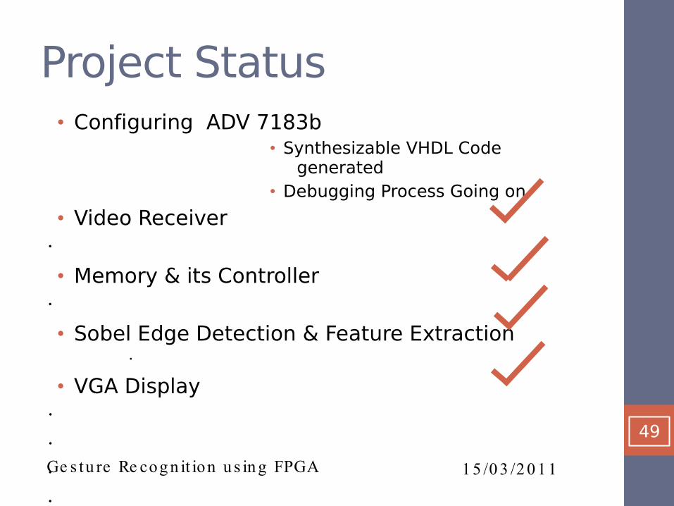
Project Status• Configuring ADV 7183b
• Synthesizable VHDL Code generated
• Debugging Process Going on
• Video Receiver
• Memory & its Controller
• Sobel Edge Detection & Feature Extraction
• VGA Display
1 5 /0 3 /2 0 1 1Ge s tu re Re cog n it ion u s in g FPGA

50
Future Applications
• Help for disabled people
• Medicine•
• Communication •
• Entertainment
1 5 /0 3 /2 0 1 1Ge s tu re Re cog n it ion u s in g FPGA

51
References[1] Digilent, “VDEC1 Reference Manual” ,
doc:502.046
[2] Analog Devices, “Multi format SDTV Video
Decoder - ADV 7183 Datasheet”, Norwood, MA,
2005
[3]Xilinx Virtex II Pro FPGA User Guide
[4]Xilinx,” Line Field Decoder”, Dec 13,2001, Greg
Hawks
[5]Xilinx University Program Virtex II Pro
Development System : Hardware Reference
Mannual,March 8th 2005
1 5 /0 3 /2 0 1 1Ge s tu re Re cog n it ion u s in g FPGA

52
Non Restoring Square Root Algorithm

53
Hirose Connector

54