Embed Size (px)
Citation preview
SCANNING TUNNELING MICROSCOPY -FROM BIRTH TO ADOLESCENCE
Nobel lecture, December 8, 1986
by
GERD BINNIG AND HEINRICH ROHRER
IBM Research Division, Zurich Research Laboratory, 8803 Rüschlikon,Switzerland
We present here the historic development of Scanning Tunneling Microscopy;the physical and technical aspects have already been covered in a few recentreviews and two conference proceedings [l] and many others are expected tofollow in the near future. A technical summary is given by the sequence offigures which stands alone. Our narrative is by no means a recommendation ofhow research should be done, it simply reflects what we thought, how we actedand what we felt. However, it would certainly be gratifying if it encouraged amore relaxed attitude towards doing science.
Perhaps we were fortunate in having common training in superconductivity,a field which radiates beauty and elegance. For scanning tunneling microscopy,we brought along some experience in tunneling [2] and angstroms [3], butnone in microscopy or surface science. This probably gave us the courage andlight-heartedness to start something which should “not have worked in prin-ciple” as we were so often told.
“After having worked a couple of years in the area of phase transitions andcritical phenomena, and many, many years with magnetic fields, I was readyfor a change. Tunneling, in one form or another had intrigued me for quitesome time. Years back, I had become interested in an idea of John Slonczewskito read magnetic bubbles with tunneling; on another occasion, I had beeninvolved for a short time with tunneling between very small metallic grains inbistable resistors, and later I watched my colleagues struggle with toleranceproblems in the fabrication of Josephson junctions. So the local study of growthand electrical properties of thin insulating layers appeared to me an interestingproblem, and I was given the opportunity to hire a new research staff member,Gerd Binnig, who found it interesting, too, and accepted the offer. Incidentally,Gerd and I would have missed each other, had it not been for K. Alex Müller,then head of Physics, who made the first contacts [l].”
The original idea then was not to build a microscope but rather to performspectroscopy locally on an area less than 100 Å in diameter.
“On a house-hunting expedition, three months before my actual start atIBM, Heini Rohrer discussed with me in more detail his thoughts on inhomo-geneities on surfaces, especially those of thin oxide layers grown on metal
390 Physics 1986
Cd)
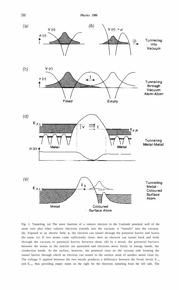
Fig. 1. Tunneling. (a) The wave function of a valence electron in the Coulomb potential well of the
atom core plus other valence electrons extends into the vacuum; it “tunnels” into the vacuum.
(b) Exposed to an electric field, ϕ, the electron can tunnel through the potential barrier and leaves
the atom. (c) If two atoms come sufficiently close, then an electron can tunnel back and forth
through the vacuum or potential barrier between them. (d) In a metal , the potential barriers
between the atoms in the interior are quenched and electrons move freely in energy bands, the
conduction bands. At the surface, however, the potential rises on the vacuum side forming the
tunnel barrier through which an electron can tunnel to the surface atom of another metal close by.
The voltage V applied between the two metals produces a difference between the Fermi levels E F,L
and EF,R, thus providing empty states on the right for the electrons tunneling from the left side. The
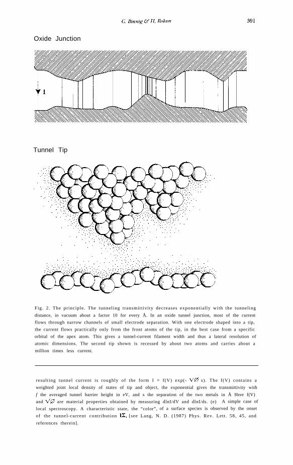
Oxide Junction
Tunnel Tip
Fig. 2. The principle. The tunneling transmitt ivity decreases exponential ly with the tunneling
distance, in vacuum about a factor 10 for every Å. In an oxide tunnel junction, most of the current
flows through narrow channels of small electrode separation. With one electrode shaped into a tip,
the current flows practically only from the front atoms of the tip, in the best case from a specific
orbital of the apex atom. This gives a tunnel-current filament width and thus a lateral resolution of
atomic dimensions. The second tip shown is recessed by about two atoms and carries about a
million times less current.
result ing tunnel current is roughly of the form I = f(V) exp(- V0 s). The f(V) contains a
weighted joint local density of states of tip and object, the exponential gives the transmittivity with
f the averaged tunnel barrier height in eV, and s the separation of the two metals in Å Here f(V)
and q/m are material properties obtained by measuring dlnI/dV and dlnI/ds. (e) A simple case of
local spectroscopy. A characteristic state, the “color”, of a surface species is observed by the onset
of the tunnel-current contribution IZ, [see Lang, N. D. (1987) Phys. Rev. Lett . 58, 45, and
references therein].
392 Physics 1986
surfaces. Our discussion revolved around the idea of how to study these filmslocally, but we realized that an appropriate tool was lacking. We were alsopuzzling over whether arranging tunneling contacts in a specific manner wouldgive more insight on the subject. As a result of that discussion, and quite out ofthe blue at the LT15 Conference in Grenoble - still some weeks before Iactually started at IBM - an old dream of mine stirred at the back of my mind,namely, that of vacuum tunneling. I did not learn until several years later thatI had shared this dream with many other scientists, who like myself, wereworking on tunneling spectroscopy. Strangely enough, none of us had evertalked about it, although the idea was old in principle.” Actually, it was 20years old, dating back to the very beginning of tunneling spectroscopy [4].Apparently, it had mostly remained an idea and only shortly after we hadstarted, did Seymour Keller, then a member of the IBM Research Division’sTechnical Review Board and an early advocate of tunneling as a new researcharea in our Laboratory, draw our attention to W.A. Thompson’s attemptingvacuum tunneling with a positionable tip [5].
We became very excited about this experimental challenge and the openingup of new possibilities. Astonishingly, it took us a couple of weeks to realize thatnot only would we have a local spectroscopic probe, but that scanning woulddeliver spectroscopic and even topographic images, i.e., a new type of micro-scope. The operating mode mostly resembled that of stylus prolilometry [6],but instead of scanning a tip in mechanical contact over a surface, a small gapof a few angstroms between tip and sample is maintained and controlled by thetunnel current flowing between them. Roughly two years later and shortlybefore getting our first images, we learned about a paper by R. Young et al. [7]where they described a type of field-emission microscope they called “topogra-liner”. It had much in common with our basic principle of operating the STM,except that the tip had to be rather far away from the surface, thus on highvoltage producing a field-emission current rather than a tunneling current andresulting in a lateral resolution roughly that of an optical microscope. Theysuggested to improve the resolution by using sharper field-emission tips, evenattempted vacuum tunneling, and discussed some of its exciting prospects inspectroscopy. Had they, even if only in their minds, combined vacuum tunnel-ing with scanning, and estimated that resolution they would probably haveended up with the new concept, Scanning Tunneling Microscopy. They camecloser than anyone else.
Mid-January 1979, we submitted our first patent disclosure on STM. EricCourtens, then deputy manager of physics at the IBM Rüschlikon Laboratory,pushed the disclosure to a patent application with “thousands of futureSTM’s”. He was the first believer in our cause. Shortly afterwards, followingan in-house seminar on our STM ideas, Hans-Jörg Scheel became the third.
For the technical realization of our project, we were fortunate in securing thecraftsmanship of Christoph Gerber. “Since his joining IBM in 1966, Christophhad worked with me (HR) on pulsed high-magnetic fields, on phase diagrams,and on critical phenomena. By the end of 1978, we were quite excited about ourfirst experimental results on the random-field problem, but when asked to
G. Binnig & H. Rohrer 393
participate in the new venture, Christoph did not hesitate an instant. Healways liked things which were out of the ordinary, and, incidentally, was thesecond believer. This left me and the random-field problem without his diligenttechnical support. About a year later, Edi Weibel was the next one to join in,which left another project without technical support. Finally, I completed theteam, leaving the random-field problem to others.”
During the first few months of our work on the STM, we concentrated on themain instrumental problems and their solutions [8]. How to avoid mechanicalvibrations that move tip and sample against each other? Protection againstvibrations and acoustical noise by soft suspension of the microscope within avacuum chamber. How strong are the forces between tip and sample? Thisseemed to be no problem in most cases. How to move a tip on such a line scale?With piezoelectric material, the link between electronics and mechanics, avoid-ing friction. The continuous deformation of piezomaterial in the angstrom andsubangstrom range was established only later by the tunneling experimentsthemselves. How to move the sample on a line scale over long distances fromthe position of surface treatment to within reach of the tip? The ‘louse’. How toavoid strong thermally excited length fluctuations of the sample and especiallythe tip? Avoid whiskers with small spring constants. This led to a more generalquestion, and the most important one: What should be the shape of the tip andhow to achieve it? At the very beginning, we viewed the tip as a kind ofcontinuous matter with some radius of curvature. However, we very soonrealized that a tip is never smooth because of the finite size of atoms, andbecause tips are quite rough unless treated in a special way. This roughnessimplies the existence of minitips as we called them, and the extreme sensitivityof the tunnel current on tip-sample separation then selects the minitip reachingclosest to the sample.
Immediately after having obtained the first stable STM images showingremarkably sharp monoatomic steps, we focused our attention onto atomicresolution. Our hopes of achieving this goal were raised by the fact thatvacuum tunneling itself provides a new tool for fabricating extremely sharptips: The very local, high fields obtainable with vacuum tunneling at a few voltsonly can be used to shape the tip by field migration or by field evaporation.Gently touching the surface is another possibility. All this is not such acontrolled procedure as tip sharpening in field-ion microscopy, but it appearedto us to be too complicated to combine STM with field-ion microscopy at thisstage. We hardly knew what field-ion microscopy was, to say nothing ofworking with it. We had no means of controlling exactly the detailed shape ofthe tip. We repeated our trial-and-error procedures until the structures weobserved became sharper and sharper. Sometimes it worked, other times it didnot.
But first we had to demonstrate vacuum tunneling. In this endeavor, apartfrom the occurrence of whiskers, the most severe problem was building vibra-tions. To protect the STM unit also against acoustical noise, we installed thevibration-isolation system within the vacuum chamber. Our first set-up wasdesigned to work at low temperatures and in ultra-high vacuum (UHV). Low
394
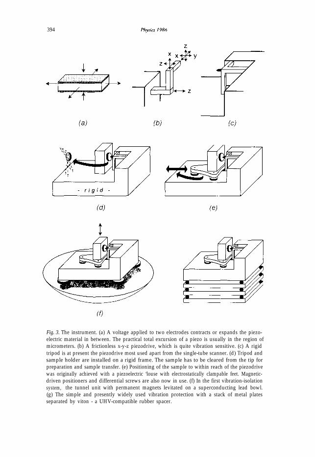
Fig. 3. The instrument. (a) A voltage applied to two electrodes contracts or expands the piezo-electric material in between. The practical total excursion of a piezo is usually in the region ofmicrometers. (b) A frictionless x-y-z piezodrive, which is quite vibration sensitive. (c) A rigidtripod is at present the piezodrive most used apart from the single-tube scanner. (d) Tripod andsample holder are installed on a rigid frame. The sample has to be cleared from the tip forpreparation and sample transfer. (e) Positioning of the sample to within reach of the piezodrivewas originally achieved with a piezoelectric ‘louse with electrostatically clampable feet. Magnetic-driven positioners and differential screws are also now in use. (f) In the first vibration-isolationsystem, the tunnel unit with permanent magnets levitated on a superconducting lead bowl.(g) The simple and presently widely used vibration protection with a stack of metal platesseparated by viton - a UHV-compatible rubber spacer.
G. Binnig & H. Rohrer 395
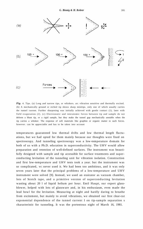
Fig. 4. Tips. (a) Long and narrow tips, or whiskers. arc vibration sensitive and thermally excited.
(b) A mechanically ground or etched tip shows sharp minitips. only one of which usually carries
the tunnel current. Further sharpening was initially achieved with gentle contact (1), later with
field evaporation (2). (c) Electrostatic and interatomic forces between t ip and sample do not
deform a blunt tip, or a rigid sample, but they make the tunnel gap mechanically unstable when the
tip carries a whisker. The response of soft materials like graphite or organic matter to such forces.
however. can be appreciable and has to be taken into account
temperatures guaranteed low thermal drifts and low thermal length fluctu-ations, but we had opted for them mainly because our thoughts were fixed onspectroscopy. And tunneling spectroscopy was a low-temperature domain forboth of us with a Ph.D. education in superconductivity. The UHV would allowpreparation and retention of well-defined surfaces. The instrument was beauti-fully designed with sample and tip accessible for surface treatments and super-conducting levitation of the tunneling unit for vibration isolation. Constructionand first low-temperature and UHV tests took a year. but the instrument wasso complicated, WC never used it. We had been too ambitious, and it was onlyseven years later that the principal problems of a low-temperature and UHVinstrument were solved [9]. Instead, we used an exsicator as vacuum chamber,lots of Scotch tape, and a primitive version of superconducting levitationwasting about 20 l of liquid helium per hour. Emil Haupt, our expert glass-blower, helped with lots of glassware and, in his enthusiasm, even made thelead bowl for the levitation. Measuring at night and hardly daring to breathefrom excitement, but mainly to avoid vibrations, we obtained our first clear-cutexponential dependence of the tunnel current I on tip-sample separation scharacteristic for tunneling. It was the portentous night of March 16, 1981.
396 Physics 1986
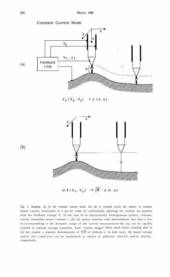
Constant Current Mode
FeedbackLoop
Fig. 5. Imaging. (a) In the constant current mode, the tip is scanned across the surface at constant
tunnel current, maintained at a pre-set value by continuously adjusting the vertical tip position
with the feedback voltage V z. In the case of an electronically homogeneous surface, constant
current essentially means constant s. (b) On surface portions with denivellations less than a few
A-cor r e spond ing to t he dynamic r ange o f t he cu r r en t measu remen t - the t i p can be r ap id ly
scanned at constant average z-position. Such “current images” allow much faster scanning than in
(a) but require a separate determination of v/m to calibrate z. In both cases, the tunnel voltage
and /o r t he z -pos i t i on can be modu la t ed t o ob t a in i n add i t i on , d ln I /dV and /o r d ln I /d s ,respectively.
G. Binnig & H. Rohrer 397
So, 27 months after its conception the Scanning Tunneling Microscope wasborn. During this development period, we created and were granted thenecessary elbow-room to dream, to explore, and to make and correct mistakes.We did not require extra manpower or funding, and our side activities pro-duced acceptable and publishable results. The first document on STM was theMarch/April 1981 in-house Activity Report.
A logarithmic dependence of the tunnel current I on tip-sample separation salone was not yet proof of vacuum tunneling. The slope of ln I versus s shouldcorrespond to a tunnel-barrier height of φ z 5 eV, characteristic of the averageworkfunctions of tip and sample. We hardly arrived at 1 eV, indicating tunnel-ing through some insulating material rather than through vacuum. Fortunate-ly, the calibration of the piezosensitivity for small and fast voltage changes gavevalues only half of those quoted by the manufacturers. This yielded a tunnel-barrier height of more than 4 eV and thus established vacuum tunneling. Thisreduced piezosensitivity was later confirmed by careful calibration with H.R.Ott from the ETH, Zurich, and of S.Vieira of the Universidad Autónoma,Madrid [10].
U. Poppe had reported vacuum tunneling some months earlier [11], but hisinterest was tunneling spectroscopy on exotic superconductors. He was quitesuccessful at that but did not measure I(s). Eighteen months later, we wereinformed that E.C. Teague, in his Thesis, had already observed similar I(s)curves which at that time were not commonly available in the open-literature
[12].Our excitement after that March night was quite considerable. Hirsh Cohen,
then Deputy Director of our Laboratory, spontaneously asked us “What do youneed?“, a simple and obvious question people only rarely dare to ask. "Gerdimmediately wanted to submit a post-deadline contribution [13] to the LT16Conference to be held in Los Angeles in September. He was going thereanyway with his superconducting strontium titanate, and I was sure we wouldhave some topographic STM images by then. And indeed we had. I arrangedan extended colloquium tour through the USA for Gerd, but about three weeksbefore his departure, a friend warned him, that once the news became public,hundreds of scientists would immediately jump onto the STM bandwagon.They did - a couple of years later. After two extended discussions on a weekendhike, he nevertheless became convinced that it was time for the STM to makeits public appearance.” Our first attempt to publish a letter failed. “That’s agood sign”, Nico Garcia, a Visiting Professor from the Universidad Autónomade Madrid, Spain consoled us.
After this first important step with a complete STM set-up, it took us onlythree months, partly spent waiting for the high-voltage power supplies for thepiezcs, to obtain the first images of monosteps [14] on a CaIrSn4 single crystalgrown by R. Gambino. Here, the main problem was getting rid of the whiskerswe continually created by bumping the tip into the surface. Now we were readyto turn to surface science, first to resolve surface reconstructions. We built aUHV-compatible STM ( no longer with Scotch tape!) and as a quick trial,
398 Physics 1986
operated it in vacuum suspended from a rubber band. The results indicatedthat superconducting levitation might be unnecessary.
That was the state of the art for the publicity tour through the USA inSeptember '81. Most reactions were benevolent, some enthusiastic, and twoeven anticipated the Nobel prize, but the STM was apparently still too exoticfor any active outside engagement.
Next, we protected the STM from vibrations by a double-stage spring systemwith eddy-current damping [8], and incorporated it in a UHV chamber not inuse at that moment. We added sputtering and annealing for sample treatment,but no other surface tool to characterize and monitor the state of the sample ortip could yet be combined with that STM. Although the superconductinglevitation served for three months only, it was cited for years. It would appearthat something complicated is much easier to remember!
A most intriguing and challenging surface-science problem existed, namely,the 7 × 7 reconstruction of the Si(111) surface. A class of fashionable modelscontained rather rough features which should be resolvable by the STM. So westarted to chase after the 7 × 7 structure, and succumbed to its magic. At first,with no success. The STM would function well, sometimes with resolutionsclearly around 5 Å, but not our surface preparation. We occasionally foundquite nice patterns with monolayer step lines [8] but usually the surface alwayslooked rough and disordered on an atomic scale. One image even foreshadowedthe 7 × 7 by a regular pattern of depressions, the precursors of the characteris-tic corner holes. However, a single event is too risky to make a case for a newstructure obtained with a new method. But it boosted our confidence.
By spring ‘82, STM was already a subject talked about. Supposedly, animage of a vicinal surface expertly prepared with a regular step sequence wouldhave eased the somewhat reserved attitude of the surface-science community.We, however, thought that the mono-, double-, and triple-steps of the CaIrSn 4
with atomically flat terraces [14] and the step lines of Si(111) [8] were convinc-ing and promising enough. And instead of wasting further time on uninterest-ing step lines, we preferred to attack surface reconstructions with knownperiodicities and with a reasonable chance of learning and contributing some-thing new.
For easier sample preparation and because the demand on resolution wasonly 8 Å, we changed to a gold single crystal, namely, the (110) surface knownto produce a 1 × 2 reconstruction. This seemed to be well within reach of theSTM resolution from what we had learned from the silicon step lines. Althoughsome time earlier, we had returned to Karl-Heinz Rieder, the Laboratory’ssurface-science expert, his Si single crystal in a kind of droplet form, it did notdeter him from proposing this gold experiment which meant lending us his Aucrystal, and some weeks later we added another droplet to his collection! But inbetween, with his advice on surface preparation, we succeeded in resolving the1 × 2 structure [15]. Contrary to expectations, we also had to struggle withresolution, because Au transferred from the surface even if we only touched itgently with our tip. The mobility of Au at room temperature is so high thatrough surfaces smooth out after a while, i. e., really sharp Au-coated tips cease
399
to exist. We should like to mention here that later, for measurements onAu(l00), we formed sharp Au tips by field evaporation of Au atoms fromsample to tip, and could stabilize them by a relatively high field resulting froma 0.8 V tunnel voltage.
In the case of the Au( 110) surface, the atomic resolution was rather a matterof good luck and perseverance. It jumped from high to low in an unpredictablemanner, which was probably caused by migrating adatoms on the tip finding astable position at the apex for a while. We also observed an appreciabledisorder leading to long but narrow ribbons of the 1·× 2 reconstruction mixedwith ribbons of 1 × 3 and 1× 4 reconstructions and step lines. Nevertheless,these experiments were the first STM images showing atomic rows with atomicresolution perpendicular to the rows. The disorder, intrinsic on this surface,but in its extent criticized from the surface-science point of view, demonstratedvery nicely the power of STM as a local method, and about a year later playedan important role in testing the first microscopic theories of scanning tunnelingmicroscopy.
With gold, we also performed the first spectroscopy experiment with anSTM. We wanted to test a prediction regarding the rectifying I-V characteris-tic of a sample-tip tunnel junction induced by the geometric asymmetry [16].Unfortunately, the sample surface became unstable at around 5 V, samplepositive, and the small asymmetry observed in this voltage range could alsohave been due to other reasons. But with reversed polarity, the voltage could beswept up to 20 V producing a whole series of marked resonant surface states[8]. We consider the gold exercise during spring and early summer of ‘82 amost important step in the development of the method, and the STM hadalready exceeded our initial expectations. We had also won our first believersoutside the Laboratory, Cal Quate from Stanford University [17] and PaulHansma from the University of California at Santa Barbara [18]. We gavenumerous talks on the Au work, and it attracted some attention but all in all,there was little action. We did not even take the time to write a paper - the 7 ×7 was waiting!
Meanwhile, we had also made the first attempts at chemical imaging: SmallAu islands on silicon. The islands were visible as smooth, flat hills on a roughsurface in the topography, but they were also clearly recognizable as regionswith enhanced tunnel-barrier height [8]. Thus, the Au islands were imagedthanks to their different surface electronic properties. It would certainly havebeen interesting to pursue this line, but we knew that, in principle, it worked,-and the 7 × 7 was still waiting!
We started the second 7 × 7 attempt in autumn 1982 taking into consider-ation the advice of Franz Himpsel not to sputter the surface. This immediatelyworked and we observed the 7 × 7 wherever the surface was flat. We wereabsolutely enchanted by the beauty of the pattern.
“I could not stop looking at the images. It was like entering a new world.This appeared to me as the unsurpassable highlight of my scientific career andtherefore in a way its end. Heini realized my mood and whisked me away for
Physics 1986
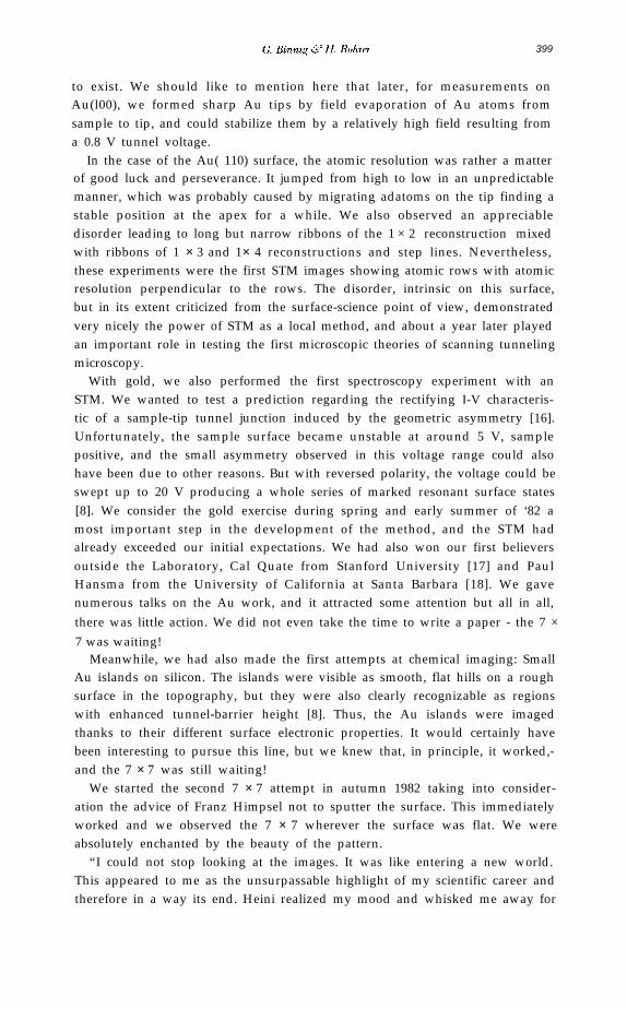
Fig. 6. 7 x 7 reconstruction of Si(111), (a) Relief assembled from the original recorder traces, from
Ref. [19], 1983 The American Physical Society, and (h) processed image of the 7 × 7 reconstruc-
tion of Si(111). Characteristic of the rhomhohedral surface unit cell are the corner hole and the 12
maxima, the adatoms. In the processed image, the six adatoms in the right half of the rhombi
appear higher. This is an electronic inequivalence on the surface owing to a structural left-right
inequivalence in the underlying layers. The reconstruction extends undisturbed to the immediate
vicinity of the large “atom hill” on the right.
G. Binnig & H. Rohrer 401
some days to St. Antönien, a charming village high up in the Swiss mountains,where we wrote the paper on the 7 × 7."
We returned convinced that this would attract the attention of our col-leagues, even of those not involved with surface science. We helped by present-ing both an unprocessed relief model assembled from the original recordertraces with scissors, Plexiglass and nails, and a processed top view; the formerfor credibility, the latter for analysis and discussion [19]. It certainly did help,with the result that we practically stopped doing research for a while. We wereinundated with requests for talks, and innumerable visitors to our Laboratorywere curious to know how to build an STM. However, the number of groupsthat seriously got started remained small. It seemed there was still a conflictbetween the very appealing, conceptual easiness of displaying individual atomsin three-dimensional real space direct by recorder traces, and the intuitivereservation that, after all, it just could not be that simple.
Our result excluded all the numerous models that existed, and strangelyenough also some that followed. Only one came very close: The adatom modelby W. Harrison [20] with just the number of adatoms not quite right. Nowa-days, a variation of the adatom model where deeper layers are also reconstruct-ed besides the characteristic 7 × 7 adatom pattern [21], is generally acceptedand compatible with most results obtained by various experimental methodslike ion channeling [22], transmission electron diffraction [23], and moredetailed STM results from other groups [24].
The 7 × 7 experiments also accelerated the first theoretical efforts of STM ona microscopic level. Tersoff and Hamman, and Baratoff [25] applied Bardeen’stransfer Hamiltonian formalism to the small geometries of tip and an atomical-ly corrugated surface. Garcia, Ocal, and Flores, and Stoll, Baratoff, Selloni,and Carnevali worked out a scattering approach [26]. The two approachesconverged; they consoled us by roughly confirming our intuitive view ontunneling in small geometries by simply scaling down planar tunneling, andthey certainly improved the acceptance of STM in physics circles. The theoreti-cal treatments concentrated on the nonplanar aspect of tunneling of freeelectrons, and the STM results on Au(110), still unpublished, served as atesting ground. They remained unpublished for quite some time, since theflashy images of the 7 × 7 silicon surface somehow overshadowed the earlierAu( 110) experiments. One reaction to the first attempt to publish them was:“ ... The paper is virtually devoid of conceptual discussion let alone conceptualnovelty... I am interested in the behavior of the surface structure of gold andthe other metals in the paper. Why should I be excited about the results in thispaper?...” It was certainly bad publication management on our part, but wewere not sufficiently familiar with a type of refereeing which searches for weakpoints, innocently ignoring the essence.
The gold and silicon experiments showed that STM in surface science wouldbenefit greatly from additional, in-situ surface characterization, in particularlow-energy electron diffraction (LEED). We had already learned that surfaces,even elaborately prepared, were frequently not as uniform and flat as generallyassumed. The in-situ combination of LEED with STM proved extremely
402 Physics 1986
helpful, avoiding searching when there was nothing to be searched, and it gaveus the opportunity to learn about and work with LEED and Auger electronspectroscopy (AES). The combination of STM with other established surface-science techniques also settled a concern frequently mentioned: How much didour STM images really have in common with surfaces characterized otherwise?We did not share this concern to such a degree, as we had also learned thatreconstructions extended unchanged to the immediate vicinity of defect areas,and because we could detect most contaminants or defects individually. Thus,for us, the combined instrumentation was more a practical than a scientificissue.
After a short but interesting excursion with the new STM/LEED/AEScombination into resolving and understanding the (100) surface of Au [27], weproceeded into the realms of chemistry. Together with A. Baró, a VisitingProfessor from Universidad Autónoma de Madrid, Spain, who also wanted tofamiliarize himself with the technique, we observed the oxygen-induced 2 × XgtÖ®³spºq£D·×±gtÖ®³spºq£D·×± 1reconstruction of Ni( 110) [28], interpreting the pronounced and regularlyarranged protrusions we saw as individual oxygen atoms. We had seen atomic-scale features before, which could be interpreted as adsorbates or adsorbateclusters but they were more a nuisance than a matter of interest. The oxygen onNi experiments demonstrated that the oxygen overlayer was not irreversiblychanged by the imaging tunnel tip. This was a most significant result in regardto observing, studying and performing surface chemistry with an STM tip.About a year later, when studying the oxygen-induced 2 × 2 reconstructedNi(l00) surface, we observed characteristic current spikes which we couldattribute to oxygen diffusing along the surface underneath the tip [29]. Wenoted that the same type of spikes had already been present in our earlierimages of oxygen-covered Ni(110), but had been discarded at that time. Notonly could diffusing atoms be observed individually, but their migration couldbe correlated to specific surface features like step lines or bound oxygen atoms,imaged simultaneously. Towards the end of 1983, we also started to probe thepossibilities of STM in biology together with H. Gross from the ETH, Zurich.We could follow DNA chains lying on a carbon film deposited on a Ag-coatedSi wafer [30].
That year ended with a most pleasant surprise: On Friday December 9, wereceived a telegram from the secretary of the King Faisal Foundation, followedon Monday by a phone call from the secretary of the European Physical Societyannouncing the King Faisal Prize of Science and the Hewlett Packard Euro-physics Prize, respectively. “The day the telegram arrived, Gerd was in Berlindelivering the Otto Klung Prize lecture. It was also my twentieth anniversarywith IBM.” This was an encouraging sign that Scanning Tunneling Micro-scopy was going to make it. It also brought a new flood of requests.
In the summer of 1984, we were finally ready to assume what we had set outto do in autumn 1978, before the notion of microscopy had ever evolved,namely, performing local spectroscopy. Together with H. Fuchs and F. Salvan,we investigated the clean 7 × 7 [ 1, 3 1] and the d/3 × d/3 Au reconstructions onSi(111) [31], and-right back to the heart of the matter-a thin oxide film on Ni
G. Binnig & H. Rohrer 403
[1,32]. We could see that surfaces are electronically structured as known, forexample, from photoemission experiments, and that we could resolve theseelectronic structures in space on an atomic scale. We called this (and still do)the color of the atoms. Indeed, the oxide layers were inhomogeneous and mostclearly visible in scanning tunneling spectroscopy (STS) images. On the 7 x 7,we could see by STS down to the second layer, and observe individual danglingbonds between the adatoms [1]. At that time, C. Quate and his group alreadyhad an STM running, and they had performed local spectroscopy; not yet withatomic resolution but a low temperature [33]. They had measured the energygap of a superconductor, and later even plotted its spatial dependence. Spec-troscopic imaging was not really surprising, yet it was an important develop-ment. We now had the tools to fully characterize a surface in terms of topo-graphic and electronic structure. Although it is usually quite an involvedproblem to separate the property of interest from a set of STM and STSmeasurements, our vision of the scanning tunneling microscope had becometrue. But nevertheless, we heard that this view was not generally shared.Rumors reached us that scientists would bet cases of champagne that ourresults were mere computer simulations! The bets were probably based on thefact the STM was already three years old, and atomic resolution was still ourexclusive property. This was also our concern, but in another way. In latesummer ‘83, Herb Budd, promoter of the IBM Europe Institute and anenthusiastic STM supporter, had asked us to run an STM Seminar in summer1984 within the framework of the Institute. This meant one week with 23lectures in front of a selected audience of the European academia. At that time,there was no way whatsoever of filling 23 hours, let alone of committing 23speakers. A year later, we agreed, full of optimism for summer ‘85. In De-cember ‘84, on Cal Quate’s initiative, nine representatives of the most ad-vanced STM groups came together for a miniworkshop in a hotel room inCancun. It was a most refreshing exchange of ideas, but there was still no otheratomic resolution, and thus not a sufficient number of lectures in sight for theSeminar.
In the following few months, the situation changed drastically. R. Feenstraand coworkers came up first with cleaved GaAs [34], C.F. Quate’s group withthe 1 X 1 structure on Pt(l00) [35], and J. Behm, W. Hoesler, and E. Ritterwith the hexagonal phase on Pt(l00) [36]. At the American Physical SocietyMarch Meeting in 1985, P. Hansma presented STM images of graphite struc-tures of atomic dimensions [37], and when J. Golovchenko unveiled the beauti-ful results on the various reconstructions of Ge films deposited on Si(111) [38],one could have heard a pin drop in the audience. The atomic resolution wasofficial and scanning tunneling microscopy accepted. The IBM Europe Insti-tute Seminar in July turned into an exclusive workshop for STM’ers, andcomprised some 35 original contributions, not all of them on atomic resolution,but already more than in March [39]. “A watershed of ideas” as Cal Quateexpressed it.
Our story so far has dealt mainly with the striving for structural andelectronic imaging in a surface-science environment with atomic resolution.
404 Physics 1986
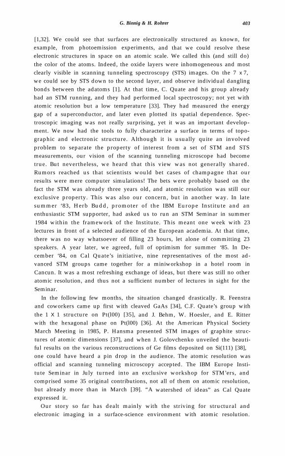
Fig. 7. STM image of cleaved graphite. The top image was taken at a constant tunnel current of
1 nA and at 50 mV. The corrugation traced by the tip reflects the local density of states (LDOS) at
the Fermi level and not the positions of atoms, which form a flat honeycomb lattice as indicated.
The LDOS at the atoms bound to the neighbors in the second layer (open circles) is lower than at
the “free” atoms. The image is thus rather a spectroscopic than a topographic one. The middle
image is a “current image” showing essentially the same pattern. In the bottom current image,
taken closer to the surface, the two inequivalent atoms appear practically identical. This peculiar
behavior is compatible with a different local elastic response of the two types of carbon atoms to the
interatomic force exerted by the tip compensating for their different LDOS. A local perturbation of
the electronic structure might also be important.
G. Binnig & H. Rohrer 405
Individual atoms had been seen before with field-ion microscopy, and dealtwith individually by the atom probe technique [40]. The beauty of thesetechniques is relativized by the restriction to distinct atom sites on fine tipsmade from a rather limited selection of materials. Similarly, electron micros-copy, the main source of present-day knowledge on submicron structures inpractically all areas of science, technology, and industry, has advanced to theatomic level. Imaging of individual atoms or atomic structures, however, is stillreserved for specific problems, expertise, and extraordinary equipment. Theappeal and the impact of STM lie not only in the observation of surfaces atomby atom, but also in its widespread applicability, its conceptual and instrumen-tal simplicity and its affordability, all of which have resulted in a relaxed andalmost casual perception of atoms and atomic structures.
But there are many other aspects, maybe less spectacular but nonethelesssignificant, which have made STM an accepted and viable method now pur-sued in many areas of science and technology.
The instruments themselves have become simpler and smaller. Their greatlyreduced size allows easy incorporation into other systems, for instance, into ascanning electron microscope [41]. One type of instrument retains accuratesample positioning but is sufficiently rigid for in-situ sample and tip exchange.Other instruments are so rigid they are even insensitive to vibrations whenimmersed in liquid nitrogen [42], and even small enough to fit through the neckof a liquid-helium storage vessel [43]. These humming-birds of STM, someconcepts of which reach back to the squeezable tunnel junctions [18], can alsooperate at television speed on relatively flat surfaces using single-tube scanners[43, 44]. Also tip preparation has advanced to a level where well-definedpyramidal tips ending with one [45] or more [46] atoms can be fabricated in aUHV environment. Such tips are particularly important for investigations ofnonperiodic structures, disordered systems and rough surfaces. They are alsointeresting in their own right, for example, as low-energy electron and ion pointsources.
Outside the physics and surface-science communities, the various imagingenvironments and imaging capabilities seem as appealing as atomic resolution.Images obtained at ambient-air pressure were first reported in 1984 [47],followed by imaging in cryogenic liquids [42], under distilled water [48], insaline solutions [48], and in electrolytes [49]. Scanning tunneling poten-tiometry appears to have become an interesting technique to study the poten-tial distribution on an atomic scale of current-carrying microstructures [50].More recent advances include interatomic-force imaging with the atomic-forcemicroscope [51], with which the structure and elastic properties of conductorsand insulators are obtained, and combined imaging of electronic and elasticproperties of soft materials [52]. Also the use of spin polarized electron tunnel-ing to resolve magnetic surface structures is being explored.
Finally, we revert to the point where the STM originated: The performanceof a local experiment, at a preselected position and on a very small spatial scaledown to atomic dimensions. Besides imaging, it opens, quite generally, newpossibilities for experimenting, whether to study nondestructively or to modify
406 Physics 1986
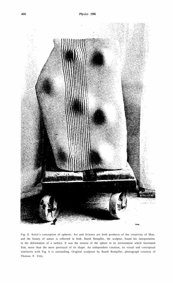
Fig. 8. Artist’s conception of spheres. Art and Science are both products of the creativity of Man,
and the beauty of nature is reflected in both. Ruedi Rempfler, the sculptor, found his interpretation
in the deformation of a surface. It was the tension of the sphere in its environment which fascinated
him, more than the mere portrayal of its shape. An independent creation, its visual and conceptual
similarity with Fig. 6 is astounding. Original sculpture by Ruedi Rempfler, photograph courtesy of
Thomas P. Frey.
G. Binnig & H. Rohrer 407
locally: Local high electric fields, extreme current densities, local deformations,measurements of small forces down to those between individual atoms, just toname a few, ultimately to handle atoms [53] and to modify individual mole-cules, in short, to use the STM as a Feynman Machine [54]. This area has notyet reached adolescence.
The STM’s “Years of Apprenticeship” have come to an end, the fundamen-tals have been laid, and the “Years of Travel” begin. We should not like tospeculate where it will finally lead, but we sincerely trust that the beauty ofatomic structures might be an inducement to apply the technique to thoseproblems where it will be of greatest service solely to the benefit of mankind.Alfred Nobel’s hope, our hope, everybody’s hope.
ACKNOWLEDGEMENT
We should like to thank all those who have supported us in one way or another,and those who have contributed to the development of Scanning TunnelingMicroscopy, and express our appreciation of the pleasant and collegial atmo-sphere existing in the STM community. Thanks are also due to Dilys Brüll-mann for her diligent handling of our manuscripts from the start and for hercareful reading of this manuscript, and to Erich Stoll for processing Figs. 6 and7 using ideas of R. Voss.
408 Physics 1986
REFERENCES
[l] For reviews, see Binnig, G., and Rohrer, H. (1986) IBM J. Res. Develop. 30, 355;Golovchenko, J. A. (1986) Science 232, 48; Behm, R. J., and Hoesler, W. (1986)Physics and Chemistry of Solid Surfaces , Vol VI, (Springer Verlag, Berlin), p. 361;Hansma, P. K., and Tersoff, J. (1987) J. Appl. Phys. 61, RI; Proceedings of theSTM Workshops in Oberlech, Austria, July 1-5, 1985, IBM J. Res. Develop. 30,Nos. 4 and 5 (1986); Proceedings of STM ‘86, Santiago de Compostela, Spain, July14- 18, 1986, Surface Sci., 181, Nos. 1 and 2 (1987). An article combining technicaland biographical details is presented in Dordick, Rowan L. (1986) IBM ResearchMagazine 24, 2.
[2] Binnig, G. K., and Hoenig, H. E. (1978) Z. Phys. B 32, 23.[3] Rohrer, H. (1960) Helv. Phys. Acta 33, 675.[4] Giaever, I. (1974) Rev. Mod. Phys. 46, 245.[5] Thompson W. A., and Hanrahan, S. F. (1976) Rev. Sci. Instrum. 47, 1303.[6] Williamson, B. P. (1967) Proc. Inst. Mech. Eng. 182,21; Guenther, K. H., Wierer,
P. G., and Bennett, J. M. (1984) Appl. Optics 23, 3820.[7] Young, R., Ward, J., and Scire, F. (1972) Rev. Sci. Instrum. 43, 999.[8] For technical details, see Binnig, G., and Rohrer, H. (1982) Helv. Phys. Acta 5.5,
726; idem (1983) Surface Sci. 126, 236; idem (1985) Sci. Amer. 253, 50.[9] Marti, 0. (1986) Ph.D. Thesis No. 8095, ETH Zurich, Switzerland; Marti, O.,
Binnig, G., Rohrer, H., Salemink, H., (1987) Surface Sci., 181, 230.[10] Ott, H. R., and Rohrer, H. (1981) unpublished; Vierira, S. (1986) IBM J. Res.
Develop. 30, 553.[11] Poppe, U. (1981) Verhandl. DPG (VI) 16, 476.[12] Teague, E. C. (1978) Dissertation, North Texas State Univ., Univ. Microfilms
International, Ann Arbor, Mich., p. 141; idem (1978) Bull. Amer. Phys. Soc. 23,290; idem (1986) J. Res. Natl. Bur. Stand. 91, 171.
[13] Binnig, G., Rohrer, H., Gerber, Ch., and Weibel, E. (1982) Physica B 109 & 110,2075.
[14] Binnig, G., Rohrer, H., Gerber, Ch., and Weibel, E. (1982) Phys. Rev. Lett. 49,57.[15] Binnig, G., Rohrer, H., Gerber, Ch., and Weibel, E. (1983) Surface Sci. 131, L379.[16] Miskowsky, N. M., Cutler, P. H., Feuchtwang, T. E. Shepherd, S. J., Lucas, A. A.,
and Sullivan, T. E. (1980) Appl. Phys. Lett. 37, 189.[17] Quate, C. F. (1986) Physics Today 39, 26.[18] Moreland, J., Alexander, S., Cox, M., Sonnenfeld, R., and Hansma, P. K. (1983)
Appl. Phys. Lett. 43, 387. Actually, Paul Hansma was indisposed and could notattend the first seminar given on STM in the USA. However, his studentsattended, and with them Paul built the squeezable tunnel junction.
[19] Binnig, G., Rohrer, H., Gerber, Ch., and Weibel, E. (1983) Phys. Rev. Lett. 50,120.
[20] Harrison, W. A. (1976) Surface Sci. 55, 1.[21] Takayanagi, K., Tanishiro, Y., Takahashi, M., and Takahashi, S. (1985) J. Vac.
Sci. Tech. A 3, 1502.[22] Tromp, R. M., and van Loenen, E. J. (1985) Surface Sci. 155,441.[23] Tromp, R. M. (1985) Surface Sci. 155, 432, and references therein.[24] Becker, R. S., Golovchenko, J. A., McRae, E. G., and Swartzentruber, B. S. (1985)
Phys. Rev. Lett. 55, 2028; Hamers, R. J., Tromp, R. M., and Demuth, J. E. (1986)Phys. Rev. Lett. 56, 1972.
[25] Tersoff, J., and Hamann, D. R. (1983) Phys. Rev. Lett. 50, 1998; Baratoff, A.( 1984) Physica 127B, 143.
[26] Garcia, N., Ocal, C., and Flores, F. (1983) Phys. Rev. Lett. 50, 2002; Stoll, E.,Baratoff, A., Selloni, A., and Carnevali, P. (1984) J. Phys. C 17, 3073.
[27] Binnig; G., Rohrer, H., Gerber, Ch., and Stoll, E. (1984) Surface Sci. 144, 321.
G. Binnig & H. Rohrer 409
[28] Baró, A. M., Binnig, G., Rohrer, H., Gerber, Ch., Stoll, E., Baratoff, A., andSalvan, F. (1984) Phys. Rev. Lett. 52, 1304.
[29] Binnig, G., Fuchs, H., and Stoll, E. (1986) Surface Sci., 169, L295.[30] Binnig, G., and Rohrer, H. (1984) Tren sd in Physics, editors, J. Janta and J.
Pantoflicek (European Physical Society) p. 38.[31] Baratoff, A., Binnig, G., Fuchs, H., Salvan, F., and Stoll, E. (1986) Surface Sci.,
168, 734.[32] Binnig, G., Frank, K. H., Fuchs, H., Garcia, N., Reihl, B., Rohrer, H., Salvan, F.,
and Williams, A. R. (1985) Phys. Rev. Lett. 55, 991; Garcia, R., Saenz, J. J., andGarcia, N. (1986) Phys. Rev. B 33, 4439.
[33] de Lozanne, A. L., Elrod, S. A., and Quate, C. F. (1985) Phys. Rev. Lett. 54, 2433.[34] Feenstra, R. M., and Fein, A. P. (1985) Phys. Rev. B 32, 1394.[35] Elrod, S. A., Bryant, A., de Lozanne, A. L., Park, S., Smith, D., and Quate, C. F.
(1986) IBM J. Res. Develop. 30, 387.[36] Behm, R. J., Hoesler, W., Ritter, E., and Binnig, G. (1986) Phys. Rev. Lett. 56,
228.[37] Hansma, P. K. (1985) Bull. Amer. Phys. Soc. 30, 251.[38] Becker, R. S., Golovchenko, J. A., and Swartzentruber, B. S. (1985) Phys. Rev.
Lett. 54, 2678.[39] Proceedings published (1986) IBM J. Res. Develop. 30, 4/5.[40] For a review, see Ernst, N., and Ehrlich, G. (1986) Topics in Current Physics, Vol. 40,
editor U. Gonser (Springer Verlag, Berlin) p. 75.[41] Gerber, Ch., Binnig, G., Fuchs, H., Marti, O., and Rohrer, H. (1986) Rev. Sci.
Instrum. 57, 221.[42] Coleman, R. V., Drake, B., Hansma, P. K., and Slough, G. (1985) Phys. Rev.
Lett. 55, 394.[43] Smith, D. P. E., and Binnig, G. (1986) Rev. Sci. Instrum. 57, 2630.[44] Bryant, A., Smith, D. P. E., and Quate, C. F. (1986) Appl. Phys. Lett. 48, 832.[45] Fink, H.-W., (1986) IBM J. Res. Develop. 30,460.[46] Kuk, Y., and Silverman, P. J. (1986) Appl. Phys. Lett. 48, 1597.[47] Baró, A. M., Miranda, R., Alaman, J., Garcia, N., Binnig, G., Rohrer, H., Gerber,
Ch,. and Carrascosa, J. L. (1985) Nature 315, 253.[48] Sonnenfeld, R., and Hansma, P. K. (1986) Science 232, 211.[49] Sonnenfeld, R., and Schardt, B. C. (1986) Appl. Phys. Lett. 49, 1172.[50] Muralt, P., and Pohl, D. W’. (1986) Appl. Phys. Lett. 48, 514.[51] Binnig, G., Quate, C. F., and Gerber, Ch. (1986) Phys. Rev. Lett. 56,930.[52] Soler, J. M., Baró, A. M., Garcia, N., and Rohrer, H. (1986) Phys. Rev. Lett. 57,
444; Dürig, U., Gimzewski, J. K., and Pohl, D. W. (1986) Phys. Rev. Lett. 57,2403.
[53] Becker, R. S., Golovchenko, J. A., and Swartzentruber, B. S. (1987) Nature 325,419.
[54] Feynman, R. P. (1960) Engr. and Sci., 22, February; Hameroff, S., Schneiker, C.,Scott, A., Jablonka, P., Hensen, T., Sarid, D., and Bell, S. (1987).