Embed Size (px)
Citation preview

1 | US DOE Geothermal Program eere.energy.gov
Public Service of Colorado Ponnequin Wind Farm
Geothermal Technologies Program 2010 Peer Review
300°C Capable Electronics Platform andTemperature Sensor System For EnhancedGeothermal Systems
Vinayak TilakGE Global Research
High Temperature tools and drillingMay 18, 2010
This presentation does not contain any proprietary confidential, or otherwise restricted information.
Silicon Carbide Integrated Circuit
2 | US DOE Geothermal Program eere.energy.gov
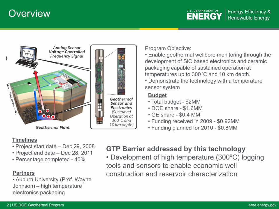
Overview
Program Objective: • Enable geothermal wellbore monitoring through the development of SiC based electronics and ceramic packaging capable of sustained operation at temperatures up to 300˚C and 10 km depth. • Demonstrate the technology with a temperature sensor system
Budget• Total budget - $2MM• DOE share - $1.6MM• GE share - $0.4 MM• Funding received in 2009 - $0.92MM• Funding planned for 2010 - $0.8MM
Timelines• Project start date – Dec 29, 2008• Project end date – Dec 28, 2011• Percentage completed - 40%
GTP Barrier addressed by this technology• Development of high temperature (300ºC) logging tools and sensors to enable economic well construction and reservoir characterization Partners
• Auburn University (Prof. Wayne Johnson) – high temperature electronics packaging

3 | US DOE Geothermal Program eere.energy.gov
Impact of Research
Project ObjectiveDevelop electronics platform technology for operation at 300ºC and demonstrate a temperature sensor system
Benefits to Geothermal industry• Enable high temperature well construction – logging tools developed using this technology can enable economic drilling• Better reservoir characterization through long term reservoir monitoring –sensors based on this technology will be designed to operate at high temperatures for months
Key innovations• Silicon carbide based integrated circuits used for active electronics – The integrated circuits attempted in this project is one of the most complex till date on silicon carbide• Ceramic based packaging and board materials that are rated to operate at 300ºC – Traditional organic based substrates or lead based packaging materials will not be used

4 | US DOE Geothermal Program eere.energy.gov
Impact of research
2009 objectives• Develop temperature sensor system architecture and flow down specifications of the silicon carbide integrated circuit• Finalize silicon carbide active device • Demonstrate a silicon carbide based integrated circuit operating at 300ºC • Validate resistors and capacitors for 300ºC operation• Develop a high temperature capable packaging process for silicon carbide

5 | US DOE Geothermal Program eere.energy.gov
Scientific approach – choice of substrate
Combined 250Cjunction and Sub-Vt leakage with std. CMOS
Junction leakage at 250C with SOI
Silicon CarbideSilicon and SOI
Objective: For optimum performance we want to have ratio of “ON’ current to “Off” current
The band gap of SiC (3.26 eV) compared to the band gap of Si (1.12eV) is the reason for the low leakage of p-n junctions at high temperatures

6 | US DOE Geothermal Program eere.energy.gov
Scientific approach – SiC MOSFETs
n-type SiC substrate
p-type epi
n-type implant
n+ implant –0.15 um 2 um
Gate ohmicohmic Oxide
Oxide thickness = 50 nm
2
3
4
5
6
7
8
9
10
0 1 2 3 4 5 6 7 8 9 10Electric Field (VG/tox) [MV/cm]
Log 1
0(t 6
3%) [
s]
375 °C
225 °C
200 µmX200 µmSample B
10 Years
100 Years
4.6 6.53.9 5.9
1.46 dec/(MV/cm)
1.84 dec/(MV/cm)
Maximum E field of normally on device
• Normally-on transistor used as a basic building block of circuit (Vthreshold<0) • n-type implant tailored to provide the appropriate threshold voltage •SiC based gate oxidation performed using N2O precursor and followed by a NO post oxidation anneal – Leads to higher reliability and stability of the gate compared to previous generation devices and circuits• Ni used for ohmic contacts and gold used as bond pad metal
Data from L.C. Yu et al., “Oxide Reliability of SiC MOS Devices”, IEEE International Integrated Reliability Workshop Final Report, pp. 141-144 (2008)
Depletion mode – SiC MOSFETs

7 | US DOE Geothermal Program eere.energy.gov
Scientific approach – Board design
Active components to be built in the program1. 300°C capable Op amp2. 300°C capable Comparator3. 300°C voltage reference
• This circuit can be configured to convert different sensor signals to different frequencies so that we can transmit the signals on a single channel• A similar board can be built for converting pressure, fluid flow, orientation information into frequency and transmitted to the surface
Lot 1 build
Integrator Comparator PT100 Sensor
Frequency dependent signal to surface
Voltage Reference
Expected waveforms
8 | US DOE Geothermal Program eere.energy.gov
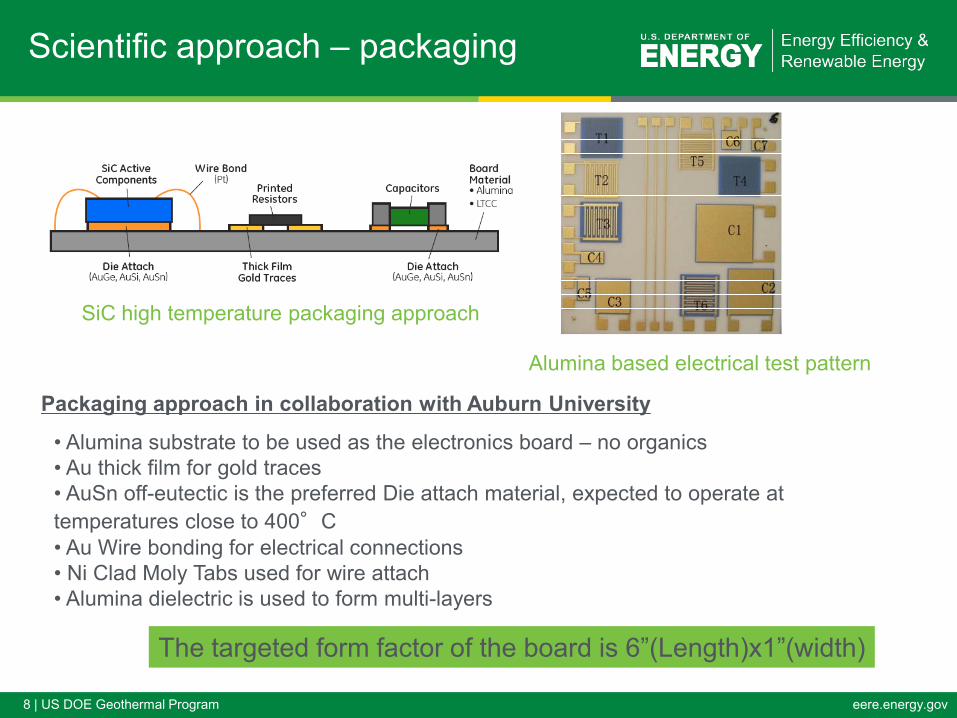
Scientific approach – packaging
• Alumina substrate to be used as the electronics board – no organics• Au thick film for gold traces • AuSn off-eutectic is the preferred Die attach material, expected to operate at temperatures close to 400°C• Au Wire bonding for electrical connections• Ni Clad Moly Tabs used for wire attach• Alumina dielectric is used to form multi-layers
Packaging approach in collaboration with Auburn University
The targeted form factor of the board is 6”(Length)x1”(width)
SiC high temperature packaging approach
Alumina based electrical test pattern

9 | US DOE Geothermal Program eere.energy.gov
Scientific approach – Passive component validation
• Highly accelerated life testing (HALT) methodologies were employed with both voltage and temperature as acceleration factors to determine lifetime at 300°C
Component Type Supplier Value Voltage Dielectric Rated Temp Capacitor A 0.1 µf 50 HT-300 300 Capacitor A 1.0 µf 50 HT-300 300 Capacitor B 0.1 µf 10 NBT, Class II 230 Capacitor C 0.1 µf 50 Class I 250 Capacitor C 0.47 µf 50 Class I 250
Component Type Supplier Value Precision Wattage Rated Temp Wire wound D 1K 1% 2 275 Wire wound D 1K 3% 0.5 250 Wire wound D 1K 3% 5.5 350 Wire wound D 10K 3% 5.5 350 Thick Film E 1K 1% 0.25 150 Thick Film E 10K 1% 0.25 150 Thick Film E 100K 1% 0.25 150 Thick Film E 1M 10% 0.25 150
−
=
211
2
2
1 11expTTk
EVV
tt a
n
Accelerated model equation

10 | US DOE Geothermal Program eere.energy.gov
Key accomplishments – SiC MOSFET 300ºC operation
0
0.0025
0.005
0.0075
0.01
0.0125
0 2 4 6 8 10 12 14 16
Drain-Source Voltage (V)
Dra
in-S
ourc
e C
urre
nt (A
)
SPICEEXPERIMENTALMEDICI
W/L=300um/6umT=300K
0
0.001
0.002
0.003
0.004
0.005
0 2 4 6 8 10 12 14 16
Drain-Source Voltage (V)
Dra
in-S
ourc
e C
urre
nt (A
)
SPICEEXPERIMENTALMEDICI
W/L=300um/6umT=300C
Parameters 300K 573KVthreshold -9V -8.5V
Idsat 30 mA/mm 10 mA/mm
Gm 4.6 mS/mm 1.7mS/mm
Rsheet(resistor) 11.8 kΩ/sq 41.8 kΩ/sq
Key MOSFET parameters at RT and 300C
Model features• Scalable by setting the values of W and L • Body effect on Drain and Source series resistance modeled with M1 and M2 FETs • DC model (no capacitances included) • Predictive of on-state I-V, does not model off-state leakage current
300ºC
RT

11 | US DOE Geothermal Program eere.energy.gov
Key accomplishments – SiC op amp operation at 300ºC
Room Temperature 300C
60dB gain @ 1kHz 57.9dB gain @ 1kHz
OpAmp
-5V
5mVp-p
V-
V+
Vout
input
output
Picture of SiC op amp
3mm
The op amp circuit consists of 15 transistors and 17 resistors

12 | US DOE Geothermal Program eere.energy.gov
Key accomplishments – SiC high temperature circuit stability
Common-source amplifier
• The circuits were stressed so that maximum current flows through the transistor at 300ºC• Very little drift of gain and input-output curves seen at 300ºC• The dramatic improvement in stability and reliability compared to previous generations of SiC ICs is attributed to the improvement in the SiC gate oxidation process

13 | US DOE Geothermal Program eere.energy.gov
Key accomplishments – lifetime of capacitors
0.1uF COG (C1210C104K5GAC)
0
20
40
60
80
100
120
140
0 100 200 300 400
Temperature (C)
Cap
acita
nce
(nF)
10.0%50.0%90.0%
10 100
10
100
1000
10000
100000
Voltage
Tim
e to
Fai
lure
ReliaSoft Weibull++ 7 - www.ReliaSoft.com
Probability - Weibull
Kemet\Kemet0.1-300C290V: β=0.7423, η=9.4541, ρ=0.9270Kemet\Kemet0.1-300C200V: β=2.5232, η=32.5467, ρ=0.9737Kemet\Kemet0.1-300C100V: β=5.5527, η=294.3067, ρ=0.9849
Time, (t)
Unrel
iabilit
y, F(
t)
0.010 1000.0000.100 1.000 10.000 100.0001.000
5.000
10.000
50.000
90.000
99.000 Probability-Weibull
Kemet\Kemet0.1-300CWeibull-2PRRX SRM MED FMF=10/S=0
Data PointsProbability Line
Kemet\Kemet0.1-300C2Weibull-2PRRX SRM MED FMF=10/S=0
Data PointsProbability Line
Kemet\Kemet0.1-300C2Weibull-2PRRX SRM MED FMF=10/S=0
Data PointsProbability Line
David ShaddockGeneral Electric Resear11/12/20099:43:31 AM
Value: 0.10uF, 50V, H dielectricTemperature: 300CVoltage Bias: 290, 200, 100Model parameters: n=3.67 using 100 and 200VEstimated Life: 17254 hrs at 25V

14 | US DOE Geothermal Program eere.energy.gov
Key accomplishments – lifetime of resistors
1 kΩ thick film resistor
ReliaSoft Weibull++ 7 - www.ReliaSoft.com
Probability - Exponential
Folio1\Data 2: λ=0.0003, γ=1083.1292, ρ=−0.9572Folio1\Data 1: λ=0.0013, γ=204.1489
Time, (t)
Relia
bility
, R(t)
100.000 3000.000680.000 1260.000 1840.000 2420.0001.000
5.000
10.000
50.000
99.000 Probability-Exponenti
Folio1\Data 1Exponential-2PMLE SRM MED FMF=10/S=0
Data PointsProbability Line
Folio1\Data 2Exponential-2PRRX SRM MED FMF=5/S=5
Data PointsProbability Line
David ShaddockGeneral Electric Resea4/23/20103:55:29 PM
Temp=350C, 16V across DUT, 0.25W (at rating)3529 hrs, 7 failures
Mean life962.3558 hours @ 1 % degradation3994.9697 hours @ 2% degradation

15 | US DOE Geothermal Program eere.energy.gov
Key accomplishments – 300C packaging process
1 2 3 4 5 1 2 3 4 5 1 2 3 4 5 1 2 3 4 5
70
75
80
85
90
95
100
105
110
115
120
Metal on Ceramic Dielectric on Ceramic Metal on Dielectric Dielectric on Metal
Pul
l Str
engt
h (lb
)
1: As Build2: 500h3: 1000h4: 1500h5: 2000h
Adhesion of dielectric(5951), metal(5771) and alumina substrate shows very little degradation at 300C
As Build 500h 1000h 1500h 2000h0
10
20
30
40
50
60
70
80
She
ar S
tren
gth
(g)
Ball bond shear strength decreases after 1500 hours at 300C – The decrease is related to diffusion of Ti into Au in the bond pads
Key packaging steps• Deposition of dielectric and conductor on alumina substrates• Wire bonding of SiC die for electrical connection• Attachment of SiC die and passive dies on alumina substrates and dielectric
Initial die attach strength was 11.3 kg/mm2
500 hour, 320ºC die attach strength was 3.7 kg/mm2 – Sn diffusion is suspected as reason for reduction in die attach strength

16 | US DOE Geothermal Program eere.energy.gov
Key accomplishments – 300C packaging process
0 50 100 150 200 250 300 35010-12
10-11
10-10
10-9
10-8
10-7
10-6
10-5
10-4
Leak
age
Cur
rent
Den
sity
(A/c
m2)
Capacitor Leakage Current Density at 100V
c1c2c3c4c5c6c7
1 2 3 1 2 3 1 2 3
10-11
10-10
10-9
10-8
10-7
10-6
10-5
23 150 300
Leak
age
Cur
rent
Den
sity
(A/c
m2)
1: As Build2: 500h3: 1000h
Leakage of alumina substrate as a function of temperature
Leakage of alumina substrate at different times and temperatures
• Leakage of alumina substrates are in the pA range, when scaled with area at 300ºC• Leakage of alumina substrates does not increase significantly with time at 300ºC

17 | US DOE Geothermal Program eere.energy.gov
Project schedule
• Key milestones met so far• Sensor system design complete and components specified• SiC device selected• Package and process for Gen 1 board finalized
2009 Spending profile Q1 2009 - $184KQ2 2009 - $258KQ3 2009 - $190KQ4 2009 - $289K
Delay in starting second lot because of a wafer breakage incident and long lead times from SiC suppliers (see supplemental information)

18 | US DOE Geothermal Program eere.energy.gov
Project management – external collaborations and reporting
• The high temperature electronics project so far has yielded 3 publications (see supplemental slide for reference)• The results from this work will be presented at the High temperature electronics conference (HiTEC 2010)• The boards developed under the program will be tested at Sandia National Labs under a supplementary program funded by DOE• A second project for the development of telemetry module to multiplex multiple sensor inputs and to demonstrate a sensor system that consists of multiple pressure and temperature sensors operating at 300ºC has been funded by DOE through recovery act funding

19 | US DOE Geothermal Program eere.energy.gov
Future directions
Plans for FY 2010• Complete fabrication of second lot of ICs and demonstrate op amps, comparators and voltage reference operating at 300ºC – July 2010• Fabricate a high temperature board that converts temperature to frequency (Go/No-Go decision point) – August 2010• Based on results of high temperature board, design optimized SiC ICs for operation at 300ºC –November 2010
Plans for FY 2011• Complete fabrication of third lot of ICs – February 2011• Fabricate optimized high temperature board – April 2011• Complete 1000 hour testing of high temperature board – July 2011
Future Research This project will demonstrate the feasibility of using SiC electronics at 300ºC in a lab environment. If successful, the electronics will need to be field tested and is the next logical step in raising the technology readiness level (TRL).

20 | US DOE Geothermal Program eere.energy.gov
Summary
• Geothermal drilling requires high temperature sensors and tools for well construction and reservoir characterization • A key technology gap for high temperature tools us the electronics and packaging technology • Silicon carbide IC technology and ceramic packaging technology can bridge that gap
Year Key technical results2009 1. Designed a sensor system suitable for operation at 300ºC
2. Demonstrated SiC based op amp operating at 300ºC with open loop gain of 58 dB at 1 kHz – one of the most complicated ICs fabricated on SiC till date.
3. Identified and validated passive components for operation at 300ºC for 1000 hours
4. Developed a ceramic based packaging process for building an electronics board for 300ºC operation
2010 1. Fabricate a board that converts temperature to frequency based on SiC ICs and ceramic packaging
2. Design optimized SiC ICs based on results of board performance

21 | US DOE Geothermal Program eere.energy.gov
Supplemental Slides

22 | US DOE Geothermal Program eere.energy.gov
• V. Tilak, C-P Chen, P. Losee, E. Andarawis and Z. Stum, “Development of a 300ºC capable SiC based operational amplifier”, accepted for publication in the Proc. High Temperature Electronics Conf., Albuquerque, NM, May 11-13, 2010
• D. Shaddock, V. Tilak, T. Zhang, R. Zhang and R. Wayne Johnson, “Reliability assessment of passives for 300ºC using HALT”, accepted for publication in the Proc. High Temperature Electronics Conf., Albuquerque, NM, May 11-13, 2010
• R. Zhang, R. Wayne Johnson, V. Tilak, T. Zhang and D. Shaddock, “Characterization of Thick Film Technology for 300ºC Packaging”, accepted for publication in the Proc. High Temperature Electronics Conf., Albuquerque, NM, May 11-13, 2010
Publications

23 | US DOE Geothermal Program eere.energy.gov
Scientific approach – board level simulations
Targeting 1°C error in temperature from active components
Error budget
Frequency versus temperature

24 | US DOE Geothermal Program eere.energy.gov
Accomplishments – capacitors
Large temperature coefficient of capacitance > 100%
SiSc 0.1 uF capacitor HALT data (100V, 200V, 290V; 300ºC, 350ºC)
Projected lifetime of TRS capacitor at 15V is excess of 1000 hours at 350C
Group N Ea Mean
SiSc 1.85 3.5 eV 48454
CaZrO3 3.67 NA 17254

25 | US DOE Geothermal Program eere.energy.gov
Accomplishments- capacitor termination
As received After Sn stripping After immersion Au
• Commercial off-the shelf (COTS) parts use Sn termination or AgPd termination and are therefore unsuitable for operation at 300C• GE has developed a process for stripping the Sn and plating it with Au. The immersion gold is intended to preserve the solderability of the nickel surface until soldering using a high temperature solder. Nickel will diffuse through the gold at the use temperature and form a limiting oxide.

26 | US DOE Geothermal Program eere.energy.gov
Accomplishments – Transistor SPICE models
.model sic_mosfet NMOS (level 2, Gamma=1.375, PHI=3, LAMBDA=LSC, VT0=-9.2, KP=35e-6, UCRIT=3.8e4, Uexp=0.605, Utr=0.5, TOX=0.5e-7, RD=RSC, RS=RSC, W=200u, L=4u).model M1 NMOS(level1, VT0=-60, KP=KSC, GAMMA=5.5, W=W, L=L).param W=200.param L=4.param LSC=8e-3*sqrt(6/L).param RSC=150.param KSC=3e-6*(W/L)
.model sic_mosfet NMOS (level 2, Gamma=1.375, PHI=3, LAMBDA=LSC, VT0=-9.2, KP=12.4e-6, UCRIT=3.0e4, Uexp=0.58, Utr=0.5, TOX=0.5e-7, RD=RSC, RS=RSC, W=200u, L=4u).model M1 NMOS(level1, VT0=-60, KP=KSC, GAMMA=5.5, W=W, L=L).param W=200.param L=4.param LSC=12e-3*sqrt(6/L).param RSC=584.param KSC=1.1e-6*(W/L)
T= 300ºCT= RT
Model features• Does not include temperature coefficients (two models, one for RT and one for 300°C)•Level 2 SPICE model• Scalable by setting the values of W and L • Body effect on Drain and Source series resistance modeled with M1 and M2 FETs • DC model (no capacitances included) • Predictive of on-state I-V, does not model off-state leakage current

27 | US DOE Geothermal Program eere.energy.gov
Accomplishments – Resistor SPICE models
.para KSC=1.5e-6*(1+0.2*W/L)
.model M1 NMOS(level 1, VT0=-60, KP=KSC, W=W, L=L, GAMMA=5.5).param W=10.param L=260.dc V3 0 25 0.5
0.0E+00
5.0E+04
1.0E+05
1.5E+05
2.0E+05
2.5E+05
3.0E+05
3.5E+05
4.0E+05
4.5E+05
5.0E+05
0 5 10 15
Voltage Across Resistor (V)
Res
ista
nce
(Ohm
s)
Resistors are modeled as a transistor with gate and source shortedResistor behavior depends on geometry and need standard geometry to better predict behavior

28 | US DOE Geothermal Program eere.energy.gov
Scientific approach – SiC JFETs vs SiC MOSFETs
Depletion-mode MOSFET• Normally on• Low Efield intensity in drain region – Potentially higher reliability of gate oxide• Can be driven in accumulation mode to increase the performance•High mobility and performance due to the ease in scaling the device•Electron trapping may cause drift issues
GateOxide
n+n+ n-channel
P-type
n+n+ n-channel
P-type
p+
JFET•Normally on•Low Gate Voltage Operation •No gate oxide – higher gate oxide reliability and low drift due to electron trapping•Design is more challenging as the need to ensure gate does not turn on
GateOxide
n+n+ p-channel
n-type
•Enhancement-mode MOSFET•Normally off•Low power and more efficient use of semiconductor real estate •Can be scaled easily to improve performance• Low mobility due to poor oxide carbide interface leads to poor performance• Threshold voltage temperature coefficient is much larger than in other devices making analog design more complicated

29 | US DOE Geothermal Program eere.energy.gov
Program management – broken wafers
• Wafers broken by SIMS vendor – broken wafers cannot run on Stepper lithography system and hence useless for the program• New wafers were ordered and are in house• Lot was started on March 22 and is expected to be completed by June