Embed Size (px)
Citation preview

Gentle and fast atomic force microscopy with a piezoelectric scanning probe for nanorobotics
applications
This article has been downloaded from IOPscience. Please scroll down to see the full text article.
2013 Nanotechnology 24 065502
(http://iopscience.iop.org/0957-4484/24/6/065502)
Download details:
IP Address: 86.195.7.172
The article was downloaded on 22/01/2013 at 21:30
Please note that terms and conditions apply.
View the table of contents for this issue, or go to the journal homepage for more
Home Search Collections Journals About Contact us My IOPscience

IOP PUBLISHING NANOTECHNOLOGY
Nanotechnology 24 (2013) 065502 (11pp) doi:10.1088/0957-4484/24/6/065502
Gentle and fast atomic force microscopywith a piezoelectric scanning probe fornanorobotics applications
Juan Camilo Acosta1, Jerome Polesel-Maris3, Francois Thoyer3,Hui Xie4, Sinan Haliyo2 and Stephane Regnier2
1 Departamento de Automatica y Electronica, Universidad Autonoma de Occidente, Cll 25 N 115-85Km. 2 Vıa Cali-Jamundı, Colombia2 Institut des Systemes Intelligents et de Robotique, Universite Pierre et Marie Curie, CNRS UMR 7222,4 Place Jussieu, F-75252 Paris Cedex, France3 CEA, IRAMIS, Service de Physique et Chimie des Surfaces et Interfaces, F-91191 Gif-sur-Yvette,France4 The State Key Laboratory of Robotics and Systems, Harbin Institute of Technology, 2 Yikuang Str.,150080 Harbin, People’s Republic of China
E-mail: [email protected] and [email protected]
Received 23 July 2012, in final form 10 November 2012Published 22 January 2013Online at stacks.iop.org/Nano/24/065502
AbstractA novel dual tip nanomanipulation atomic force microscope (AFM) platform operating inambient conditions is presented. The system is equipped with a high frequency quartzpiezoelectric self-sensing scanning probe for fast imaging and a passive cantilever formanipulation. The system is validated by imaging and selective pushing/pulling of goldcolloid beads (diameters from 80 to 180 nm). This provides a more compact integrationcompared to an external optical lever and avoids several of its drawbacks such as opticalinterference and noise, and recalibration in the case of a moving cantilever and a fixed lasersource and photodiode sensor. Moreover, as the quartz oscillator exhibits oscillationamplitudes in the sub-picometer range with a resonant frequency in the megahertz range, thisdynamic force sensor is ideal for fast AFM imaging. Experiments show an increase by fivetimes in imaging speed compared to a classical AFM system.
(Some figures may appear in colour only in the online journal)
1. Introduction
New tools for the assembly of MEMSs and NEMSs(micro/nano electro-mechanical systems) in efficient andrepeatable ways are required today for novel applications ofnanotechnologies [1–3]. New strategies for fast micro- andnanomanipulation are in demand for the fabrication of newproof-of-concept nanosystems in laboratories, but also forindustrial production. Micro/nanoassembly in high vacuumconditions of SEM (scanning electron microscopy) appearsto be a promising approach; nevertheless, it remains veryexpensive due to the equipment cost and it is unpracticalfor industrial applications because of the requirement of
confinement of the SEM chamber [4]. The development ofmicro/nanoassembly techniques in ambient conditions couldhence remove most of these constraints and generalize theseassembly, characterization and fabrication processes [5].
Micromanipulation in ambient conditions is generallyperformed by microtweezers or atomic force microscopes(AFMs) [6–10]. The former have mainly been used forpicking and placing of micro-objects of more than 10 µm [3].Their lack of dexterity and force feedback, the adhesioneffects between the tool and the object, and their dependenceon an external visual sensing device are the primary factorsthat limit their widespread use for smaller objects. On theother hand, AFMs, compared to traditional microtweezers,
10957-4484/13/065502+11$33.00 c© 2013 IOP Publishing Ltd Printed in the UK & the USA
Nanotechnology 24 (2013) 065502 J C Acosta et al
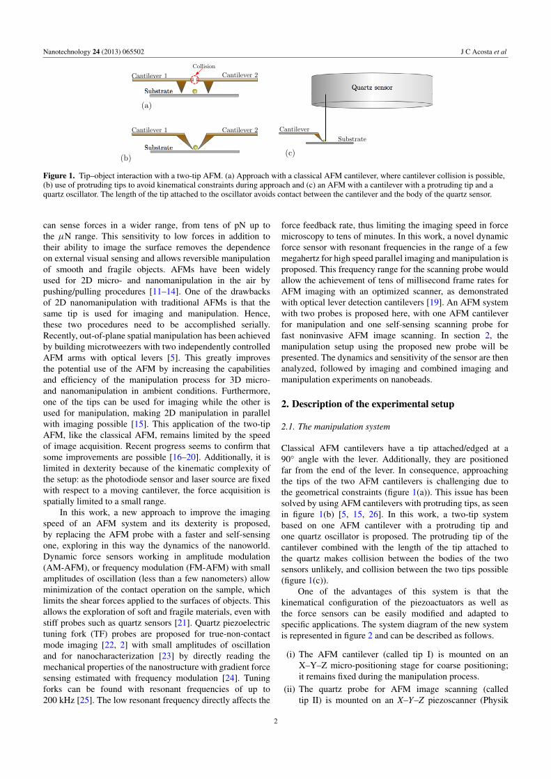
Figure 1. Tip–object interaction with a two-tip AFM. (a) Approach with a classical AFM cantilever, where cantilever collision is possible,(b) use of protruding tips to avoid kinematical constraints during approach and (c) an AFM with a cantilever with a protruding tip and aquartz oscillator. The length of the tip attached to the oscillator avoids contact between the cantilever and the body of the quartz sensor.
can sense forces in a wider range, from tens of pN up tothe µN range. This sensitivity to low forces in addition totheir ability to image the surface removes the dependenceon external visual sensing and allows reversible manipulationof smooth and fragile objects. AFMs have been widelyused for 2D micro- and nanomanipulation in the air bypushing/pulling procedures [11–14]. One of the drawbacksof 2D nanomanipulation with traditional AFMs is that thesame tip is used for imaging and manipulation. Hence,these two procedures need to be accomplished serially.Recently, out-of-plane spatial manipulation has been achievedby building microtweezers with two independently controlledAFM arms with optical levers [5]. This greatly improvesthe potential use of the AFM by increasing the capabilitiesand efficiency of the manipulation process for 3D micro-and nanomanipulation in ambient conditions. Furthermore,one of the tips can be used for imaging while the other isused for manipulation, making 2D manipulation in parallelwith imaging possible [15]. This application of the two-tipAFM, like the classical AFM, remains limited by the speedof image acquisition. Recent progress seems to confirm thatsome improvements are possible [16–20]. Additionally, it islimited in dexterity because of the kinematic complexity ofthe setup: as the photodiode sensor and laser source are fixedwith respect to a moving cantilever, the force acquisition isspatially limited to a small range.
In this work, a new approach to improve the imagingspeed of an AFM system and its dexterity is proposed,by replacing the AFM probe with a faster and self-sensingone, exploring in this way the dynamics of the nanoworld.Dynamic force sensors working in amplitude modulation(AM-AFM), or frequency modulation (FM-AFM) with smallamplitudes of oscillation (less than a few nanometers) allowminimization of the contact operation on the sample, whichlimits the shear forces applied to the surfaces of objects. Thisallows the exploration of soft and fragile materials, even withstiff probes such as quartz sensors [21]. Quartz piezoelectrictuning fork (TF) probes are proposed for true-non-contactmode imaging [22, 2] with small amplitudes of oscillationand for nanocharacterization [23] by directly reading themechanical properties of the nanostructure with gradient forcesensing estimated with frequency modulation [24]. Tuningforks can be found with resonant frequencies of up to200 kHz [25]. The low resonant frequency directly affects the
force feedback rate, thus limiting the imaging speed in forcemicroscopy to tens of minutes. In this work, a novel dynamicforce sensor with resonant frequencies in the range of a fewmegahertz for high speed parallel imaging and manipulation isproposed. This frequency range for the scanning probe wouldallow the achievement of tens of millisecond frame rates forAFM imaging with an optimized scanner, as demonstratedwith optical lever detection cantilevers [19]. An AFM systemwith two probes is proposed here, with one AFM cantileverfor manipulation and one self-sensing scanning probe forfast noninvasive AFM image scanning. In section 2, themanipulation setup using the proposed new probe will bepresented. The dynamics and sensitivity of the sensor are thenanalyzed, followed by imaging and combined imaging andmanipulation experiments on nanobeads.
2. Description of the experimental setup
2.1. The manipulation system
Classical AFM cantilevers have a tip attached/edged at a90◦ angle with the lever. Additionally, they are positionedfar from the end of the lever. In consequence, approachingthe tips of the two AFM cantilevers is challenging due tothe geometrical constraints (figure 1(a)). This issue has beensolved by using AFM cantilevers with protruding tips, as seenin figure 1(b) [5, 15, 26]. In this work, a two-tip systembased on one AFM cantilever with a protruding tip andone quartz oscillator is proposed. The protruding tip of thecantilever combined with the length of the tip attached tothe quartz makes collision between the bodies of the twosensors unlikely, and collision between the two tips possible(figure 1(c)).
One of the advantages of this system is that thekinematical configuration of the piezoactuators as well asthe force sensors can be easily modified and adapted tospecific applications. The system diagram of the new systemis represented in figure 2 and can be described as follows.
(i) The AFM cantilever (called tip I) is mounted on anX–Y–Z micro-positioning stage for coarse positioning;it remains fixed during the manipulation process.
(ii) The quartz probe for AFM image scanning (calledtip II) is mounted on an X–Y–Z piezoscanner (Physik
2

Nanotechnology 24 (2013) 065502 J C Acosta et al
Figure 2. System diagram for the new configuration of the two-tip system. The quartz is integrated into the system fortrue-non-contact-mode imaging.
Instruments, p-153.10.H) with a motion range of 10 µmand a sub-nanometer resolution on each axis. Thepiezotube is well compensated by the Prandtl–Ishlinskiioperator on its hysteresis [27] and is mounted onan X–Y–Z manual microstage. For the oscillationcontrol of the quartz oscillator, an OC4-Station fromSPECS-Nanonis (Zurich, Switzerland) is used. Thisstation has the advantage of integrating all the systems forfast dynamic AFM operation, until 5 MHz of bandwidth:a lock-in amplifier, a phase locked loop (PLL), anautomatic gain control (AGC), data acquisition hardwareand software and a real time operating system. A customhome-built transimpedance preamplifier to drive the highfrequency piezoelectric scanning probe has been built todevelop a gain of Gtrans = 6.37 M� over 4.6 MHz ofbandwidth, as illustrated in figure 3. The noise level ofdetection has been measured to be 1.57 pA Hz−1/2.
(iii) An X–Y–Z nanostage (MCL Nano-Bio2M on the X–Yaxes, PI P-732.ZC on the Z-axis) with a maximummotion range of 50 µm × 50 µm × 10 µm and aclosed loop sub-nanometer resolution is used to drive thesample.
(iv) Two data acquisition cards (National Instruments NI6289and NI6259) with resolutions of 18 and 16 bits inA/D transfer and maximum sampling frequencies of625 kHz and 1.25 MHz are used for data acquisitionfrom the optical lever, the amplifier of the cantilever andthe transimpedance preamplifier of the high frequencyquartz scanning probe, and to actuate both of theX–Y–Z piezotubes by outputting voltage signals to threeindependent high voltage amplifiers.
Figure 3. Experimental characterization of the gain and thebandwidth of the custom home-built transimpedance preamplifier todrive the high frequency piezoelectric scanning probes.
AFM imaging with the quartz oscillator tip (tip II) can becarried out by moving the substrate with the closed loop stageor by moving the sensor with the open loop piezoscanner.The latter has the advantage of avoiding movement of thesubstrate, thus keeping the distance between the cantilever tip(tip I), and substrate constant during imaging. The closed loopnanostage and tip I are used for manipulation.
2.2. Force sensor preparation
Dynamic force sensing is an alternative for increasing thespeed and the dexterity of the system. This technique has
3

Nanotechnology 24 (2013) 065502 J C Acosta et al
Figure 4. Different views of the quartz sensor. The scale bar is2.7 mm. (a) The original packaging of the quartz, (b) top view and(c)–(d) side views.
generally been used with quartz tuning forks with a typicalresonance frequency of 32.768 kHz [2]. For high speed AFM,even using frequency modulation, these sensors remain slowdue to their low data rate. In consequence, in order to takeadvantage of dynamic force sensing for AFM imaging, theuse of quartz oscillators with higher resonance frequencies ofseveral megahertz is preferable. The quartz resonators used(Citizen America CSA310) have a resonant frequency of3.579 545 MHz according to the manufacturer. The geometryof this quartz is different with a monolithic rectangular andconvex AT-cut quartz body [28] compared to the two-pronggeometry of a tuning fork. The resonance frequency, andalso the spring constant of this resonator for shear waveoscillations, is mainly determined by the material propertiesand the thickness of the crystal, as explained in detailin [28]. Figure 4 shows different views of the oscillator.The packaging (figure 4(a)) is very similar to a tuning fork:the quartz is isolated from the outside by a capsule invacuum. This capsule is mechanically removed by tweezersto transform the high frequency resonator into a scanningprobe. Then, to obtain the AFM probe, a tungsten tip(T-4-10-1 mm, tip radius 100 nm, GGB Industries) is gluedto the resonator using the electrically conductive silver epoxyEpotek H21D (Epoxy Technology). The long tip (millimeter
range) configuration of the stiff monolithic quartz probemarks another radical difference compared to a standardAFM using silicon based cantilevers with a micrometer rangetip. This needle-like configuration paves the way to newopportunities for sample access of the scanning probe, wherethe embodiment of a standard AFM cantilever can hindernanoscale imaging or mechanical characterization as its tip istoo short.
The quality factors of several scanning probes have beencharacterized as between 10 000 and 200 000, dependingon the position of the tip on the monolith and the weightof glue added. An example of frequency sweep can beseen in figure 5. For this quartz with a tip, the resonancefrequency is measured as f0 = 3.579 10104 MHz and thequality factor is Q = 125k. The stability of the OC4 PLLcontroller (SPECS-Nanonis) is given as 1 ppb d−1, but witha noise figure in the frequency, considering the probe andour preamplifier, this limits the precision for tracking theresonance frequency shift during scanning to 10 MHz. Themechanical amplitude of oscillation for the surface oscillationmode of the quartz tip is estimated as A = 166 fm with [29,30]
A =Vout
Gtrans
12π f0Kd
, (1)
where Vout and Gtrans are the output voltage and the gain ofthe transimpedance preamplifier respectively, f0 and K are thefrequency and the spring constant of the oscillation mode ofthe quartz resonator respectively and d is the piezoelectriccoefficient of the piezoelectric strain coefficient, which isequal to 3.3 pC N−1 following [29, 30] for an AT-cut quartzcrystal resonator. K = 0.636×10¹⁰ N m−1 has been estimatedfor the shear thickness mode of oscillation with [33]
K =WL
tGsπ2
2, (2)
where Gs = 31 GPa is the shear modulus of the quartz.Ignoring its convex shape, its effective dimensions are t =0.362 mm, w = 1.9 mm and L = 7.92 mm.
This sensor has a resonance frequency around a hundredtimes higher than the silicon cantilever with protruding tipused for the manipulation operation (Nanosensors ATEC-FM)[5]. This, combined with the high quality factor and stiffness,make this quartz a high speed, very sensitive sensor withamplitudes of oscillation in the sub-Angstrom range making
Figure 5. A 600 Hz frequency sweep around the resonant frequency of a quartz oscillator with a tip. (a) Amplitude and (b) phase. Theresonant frequency is estimated as f0 = 3.579 10104 MHz with 10 MHz precision with the OC4 controller and the quality factor Q = 125k.
4

Nanotechnology 24 (2013) 065502 J C Acosta et al
Figure 6. Tip attachment to the AT-cut quartz oscillator to obtain(a) a shear mode (friction forces) and (b) a normal mode(non-contact forces).
it ideal for fast true-non-contact-mode imaging. Additionally,the stiff probe avoids the jump-to-contact problem due toattractive surface forces and avoids bending during pull-offwith liquid meniscus forces due to the presence of water inair operation. In order to take advantage of the high speed ofthe sensor, the AFM controller has been improved to increasethe detection bandwidth compared to the previous versionof the two-tip nanomanipulation AFM platform publishedpreviously in [5, 15, 26].
2.3. Probe dynamics and sensitivity
The oscillation mode of rectangular AT-cut quartz resonatorshas been studied in several works [31–33]. It is knownwith precision that the AT-cut quartz resonator fundamentaloscillation mode is in the thickness shear mode, as depictedin figure 6. These oscillations are parallel to the surface.The amplitude of these oscillations decreases with thedistance to the center of the quartz. This has been validatedexperimentally with the quartz used in this paper and alsodescribed in the literature [34]. In fact, the position of theadded mass (tip with glue) has a critical role in the value ofthe final quality factor of the sensor. As the distance of theattachment from the center of the quartz increases, the higherthe quality factor is and the lower the excitation amplitude is.
at the same time, larger amplitudes of oscillation are observedin the middle area but with poor quality factors. The samemode of oscillation is also present on the other side of thesensor, but mass compensation has not been attempted tosymmetrize it. In summary, the tip is attached between themiddle of the quartz and the end to achieve a compromisebetween the oscillation amplitude and the quality factor toobtain the maximum sensitivity. This position is obtainedempirically and tends to be closer to the end than the middleof the sensor. This procedure of tip placement is reproduciblefor each monolithic resonator.
The quartz can be used as a force sensor in two differentways. The first method for force sensing with the quartzconsists in using the shear forces. This is called a lateral forcesensor [2]. For the shear mode, it is the friction force gradientbetween the tip and the surface that is probed. In this case,the tip oscillates parallel to the substrate (figure 6(a)). For thesecond method, the oscillation of the quartz is in the axis of thetip (figure 6(b)). For this, the tip needs to be attached parallelto the longitudinal axis of the quartz. This is called the normalmode and non-contact forces are used to control the distancebetween the tip and the sample.
To obtain the shear mode, the tip oscillates parallelto the substrate. This can be achieved with two differentconfigurations, the first of which is shown in figures 6(a)and 7(a), and the second of which is shown in figure 7(b).An example of a distance spectroscopy curve is illustratedin figure 8. In this case, the frequency shift increases withfriction due to the increase of contact force. It is suspectedthat the compression transmitted by the tip in the shear modeof oscillation of the monolithic resonator acts differently fora normal or a parallel strain. This point requires furtherinvestigation and deserves more numerical simulations takingthe tip into account with regard to its influence on theoscillation modes of the quartz. The set point should be assmall as possible to avoid wear of the tip and modification ofthe substrate.
It is challenging to obtain the normal mode due to thelength of the tip that needs to be attached. Additionally,the longitudinal axis of the quartz would be aligned withthe Z-axis, making the overall height of the probe too longcompared to the focal distance of the optical microscope ontop of the AFM. Thus, in order to make a probe sensitive tothe non-contact forces, the tip has been attached with an angle
Figure 7. Tip attachment to the quartz electrode to obtain (a) a shear mode with parallel attachment, (b) a shear mode with normalattachment and (c) a hybrid mode with a parallel attachment with α = 30◦.
5

Nanotechnology 24 (2013) 065502 J C Acosta et al
Figure 8. The approach/retract spectroscopy curve obtained withquartz in the lateral/shear mode on a silicon surface. The setpoint inthe frequency shift is set in the control zone.
Figure 9. The approach/retract spectroscopy curve obtained withquartz in a hybrid mode on a silicon surface. (A) Before sensing anyforce. (B) Attractive forces are dominant compared to repulsiveforces, thus 1f is positive. (C) Repulsive forces are dominant. Thesetpoint in the frequency shift can be set in either the attractive orthe repulsive control zone. Contact is estimated a few nanometersafter 1f decreases.
α (figure 7(c)). It is a hybrid configuration, and it is sensitiveto both non-contact and friction forces. For this configuration,the distance spectroscopy curve is depicted in figure 9. Thismode appears very sensitive to the attractive (B) and thenrepulsive (C) regimes of the surface forces. The tip diameterhas been determined by SEM to be about 100 nm, which mayexplain the large attractive forces observed. To control thequartz force in order to control the distance between the tipand the sample in this mode, the frequency shift setpoint canbe set in either the attractive or the repulsive zone (dashedbars on top of the curve in figure 9). The attractive regime ismore stable because the range is larger. In consequence, thesetpoint can be set far from regions of inversion of behavior,and so inversion of the controller. The controller’s parameterswere set for only one of the regions; in consequence, if there isa swap from attractive to repulsive due to noise, for example,the controller will not work. Therefore, a set point close to theinversion of behavior should be avoided. In the repulsive zonethere is a risk of hard contact of the tip with the substrate dueto the high stiffness of the sensor.
3. Results and discussion
3.1. High speed imaging with dynamic force feedback
3.1.1. Hard surface imaging. In order to validate thespeed of operation of the system and to calibrate the open
Figure 10. Raw data from the AFM scan on a hard surface with ahigh frequency quartz AFM probe for calibration of an open looppiezoscanner with a calibration substrate (HS-100MG from BudgetSensors). 20 µm (400 pixels) in the X-axis and 5 µm (100 pixels) inthe Y-axis. The image acquisition time is 12.6 s at 32 lines (X-axis)per second.
loop piezoscanner (shown in figure 2), an AFM image ofa calibration grid substrate has been made (figure 10). Onthis AFM topography map, due to the size of the pitch ofthe substrate (5 µm), the closed loop nanostage on the X–Yaxis is used to obtain a large enough lateral excursion. Forthe Z-axis the open loop piezoscanner is necessary due tothe higher resonant frequency to perform faster scanningcompared to the closed loop. The lateral dimensions of theimage are 20 µm × 5 µm. To avoid the dependence of theZ-control on the image acquisition, the trenches are alignedwith the fast axis of the scanning (X) prior to scanning withan optical microscope. The quartz used for this example isworking in a hybrid mode. The attractive forces control zoneis used for controller stability by reducing the risk of contact.The X–Y–Z-piezo controllers’ scanning speeds are manuallyset, resulting in an image acquisition time of 12.6 s. This isan important improvement of fifty times in acquisition timecompared to the acquisition speed of the previous versionof the system [15]. The AFM software controller had to beredesigned to be able to handle the increased data flow fromthe higher scanning speeds. It has been developed on a realtime operating system (Debian squeeze with rtai patch) andthe precision has increased from 1–10 ms to 1–10 µs. In thisparticular case, the controller was not set at full speed, and thestep time used with the real time operating system was twentytimes higher than the precision/latency of the system.
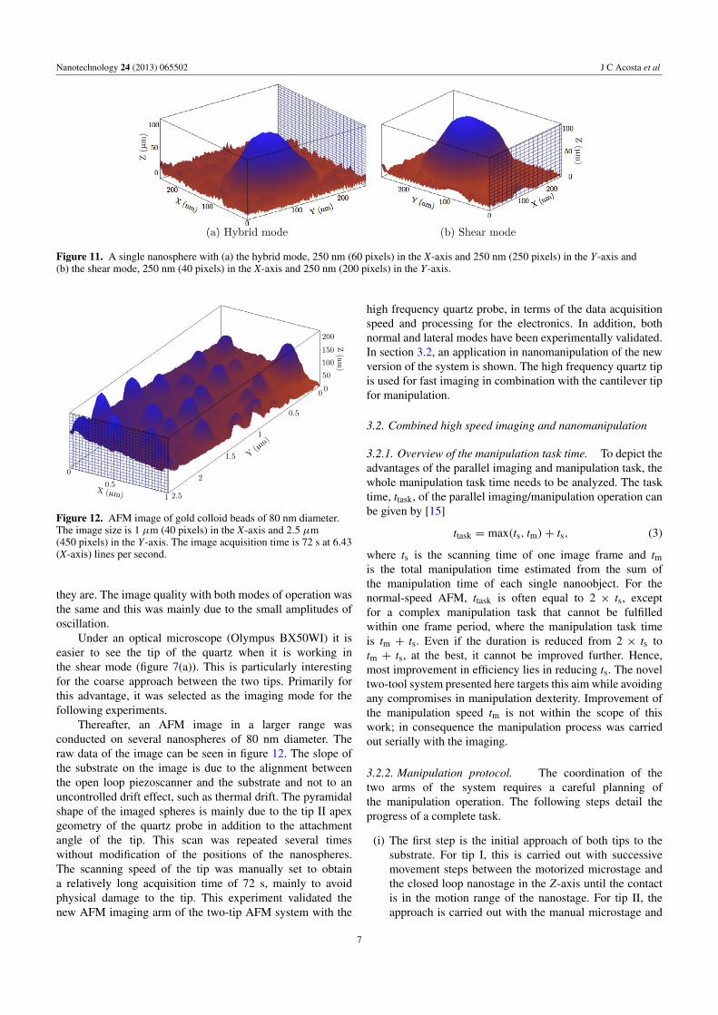
3.1.2. Imaging of loose objects on a hard surface. Afterthe experiments on hard surfaces and calibration of thepiezoscanner had been carried out, gold colloid beads ofdifferent sizes (Ted Pella, Inc) were deposited on top of asilicon substrate using the method described in [35]. Initially,two images of 150 nm diameter beads were conductedusing the hybrid force mode (figure 11(a)) and friction forcemode (figure 11(b)). This is a repeatable process and bothtechniques are noninvasive with the substrate. The diameter ofthe nanospheres was estimated using the height of the spherein the image, avoiding the lateral convolution effect of the tipend, making the dimensions seem larger in the image than
6
Nanotechnology 24 (2013) 065502 J C Acosta et al
Figure 11. A single nanosphere with (a) the hybrid mode, 250 nm (60 pixels) in the X-axis and 250 nm (250 pixels) in the Y-axis and(b) the shear mode, 250 nm (40 pixels) in the X-axis and 250 nm (200 pixels) in the Y-axis.
Figure 12. AFM image of gold colloid beads of 80 nm diameter.The image size is 1 µm (40 pixels) in the X-axis and 2.5 µm(450 pixels) in the Y-axis. The image acquisition time is 72 s at 6.43(X-axis) lines per second.
they are. The image quality with both modes of operation wasthe same and this was mainly due to the small amplitudes ofoscillation.
Under an optical microscope (Olympus BX50WI) it iseasier to see the tip of the quartz when it is working inthe shear mode (figure 7(a)). This is particularly interestingfor the coarse approach between the two tips. Primarily forthis advantage, it was selected as the imaging mode for thefollowing experiments.
Thereafter, an AFM image in a larger range wasconducted on several nanospheres of 80 nm diameter. Theraw data of the image can be seen in figure 12. The slope ofthe substrate on the image is due to the alignment betweenthe open loop piezoscanner and the substrate and not to anuncontrolled drift effect, such as thermal drift. The pyramidalshape of the imaged spheres is mainly due to the tip II apexgeometry of the quartz probe in addition to the attachmentangle of the tip. This scan was repeated several timeswithout modification of the positions of the nanospheres.The scanning speed of the tip was manually set to obtaina relatively long acquisition time of 72 s, mainly to avoidphysical damage to the tip. This experiment validated thenew AFM imaging arm of the two-tip AFM system with the
high frequency quartz probe, in terms of the data acquisitionspeed and processing for the electronics. In addition, bothnormal and lateral modes have been experimentally validated.In section 3.2, an application in nanomanipulation of the newversion of the system is shown. The high frequency quartz tipis used for fast imaging in combination with the cantilever tipfor manipulation.
3.2. Combined high speed imaging and nanomanipulation
3.2.1. Overview of the manipulation task time. To depict theadvantages of the parallel imaging and manipulation task, thewhole manipulation task time needs to be analyzed. The tasktime, ttask, of the parallel imaging/manipulation operation canbe given by [15]
ttask = max(ts, tm)+ ts, (3)
where ts is the scanning time of one image frame and tmis the total manipulation time estimated from the sum ofthe manipulation time of each single nanoobject. For thenormal-speed AFM, ttask is often equal to 2 × ts, exceptfor a complex manipulation task that cannot be fulfilledwithin one frame period, where the manipulation task timeis tm + ts. Even if the duration is reduced from 2 × ts totm + ts, at the best, it cannot be improved further. Hence,most improvement in efficiency lies in reducing ts. The noveltwo-tool system presented here targets this aim while avoidingany compromises in manipulation dexterity. Improvement ofthe manipulation speed tm is not within the scope of thiswork; in consequence the manipulation process was carriedout serially with the imaging.
3.2.2. Manipulation protocol. The coordination of thetwo arms of the system requires a careful planning ofthe manipulation operation. The following steps detail theprogress of a complete task.
(i) The first step is the initial approach of both tips to thesubstrate. For tip I, this is carried out with successivemovement steps between the motorized microstage andthe closed loop nanostage in the Z-axis until the contactis in the motion range of the nanostage. For tip II, theapproach is carried out with the manual microstage and
7

Nanotechnology 24 (2013) 065502 J C Acosta et al
Figure 13. Scan in the Y-axis with tip II to find tip I.
the open loop piezostage. Additionally, with the aid of theoptical microscope, the two tips are brought closer in theX–Y plane until tip I is within range of tip II (<10 µm).
(ii) Once the tips and the substrate are within range of thepiezoactuators, Y-axis scans are carried out with yip II inorder to find tip I (figure 13).
(iii) Now that the position of tip I is known with respect totip II, an AFM image of the substrate is scanned with tipII. The end of tip I should appear in the image as wellas the objects to manipulate. This allows the positions ofobjects with respect to tip I to be known. The open looppiezo is used to scan the surface with tip II (quartz) toavoid changing/modifying the distance between the othertip (tip 1, cantilever) and the surface. In this way, the edgeof tip I can be scanned by tip II and be seen in the AFMimage.
(iv) The next step is the 2D manipulation of nanoobjects onthe substrate (figure 14). The cantilever of tip I is used inthe static mode. The force is monitored during the entireprocess to detect the contact between tip I and the objectas well as the pushing. The closed loop nanostage is usedto move the substrate.
(v) Finally, tip II is used to scan the surface again in orderto obtain an AFM image of the substrate with the newpositions of the objects.
3.2.3. Manipulation results. The result from a manipulationtask of three gold colloid nanobeads of 80–150 nm diameterfollowing the protocol from section 3.2.2 is presented here.This result demonstrates the nanomanipulation efficiency ofthe two-tip AFM to operate in ambient conditions. Once thetwo tips are within range according to the first step, the edge oftip I in contact with the surface is found while scanning withtip II, as seen in the profile of figure 13. Hence, the relativeposition between each tip is estimated. The triangular shape inthe top of the scan in addition to the measured height allowsdifferentiation from a nanosphere.
Afterwards, an AFM image is made with tip II startingnear tip I and getting further away, as shown in figure 15(a).Once the position of the tip with respect the nanospheresis known, the nanoparticles are moved using tip I. In thisparticular case, three nanospheres were pushed to showthe manipulation capabilities of the new system with twocooperative scanning probe arms.
Figure 14. Diagonal pushing of a nanosphere. (a) Lateral bending, (b) Z-axis bending, (c) diagonal bending of the cantilever.
8

Nanotechnology 24 (2013) 065502 J C Acosta et al
Figure 15. (a) An image with tip II before manipulation. The image size is 2 µm (150 pixels) in the X-axis and 2 µm (750 pixels) in theY-axis. The image acquisition time is 108 s at 1.4 (X-axis) lines per second. (b) An image with tip II after manipulation. The image size is 2µm (60 pixels) in the X-axis and 2 µm (600 pixels) in the Y-axis The image acquisition time is 79 s at 0.76 (X-axis) lines per second.
Figure 16. Photodiode voltage during diagonal pushing of a nanosphere with tip I. (a) Lateral bending and (b) Z-axis bending.
During the pushing of the nanospheres, the lateral andnormal force behaviors are monitored with tip I, and they areestimated from the photodiode output and cantilever stiffness.An example of the output of the photodiode for diagonalpushing (figure 14(c)) of gold colloid bead number 1 canbe seen in figure 16. As a result of the diagonal pushing,forces in both the X- and Y-axes are felt. The pushing in theX-axis makes the cantilever bend up, resulting in a positivevoltage shift (figure 16(b)). In the Y-axis, the cantileverbends counter-clockwise, resulting in a negative voltage shift(figure 16(a)). The behavior between the bending of thecantilever and the sign of the voltage shift is predefined
by the geometrical configuration of the laser, cantilever andphotodiode.
The final manipulation result is depicted in figure 15(b).Nanospheres 1–3 and 5 with diameters of 120, 90, 150 and90 nm were successfully pushed with force feedback to thedesired position. In this last image, the diameter of the colloidsincreased in the X–Y-axis due to the wear of the tip; thisis a consequence of the large diameter apex of the tip usedcombined with the shear mode. The image size of 15(a) beforemanipulation is 2 µm (150 pixels) in the X-axis and 2 µm(750 pixels) in the Y-axis. The image acquisition time is108 s at 1.4 (X-axis) lines per second. The image size of
9

Nanotechnology 24 (2013) 065502 J C Acosta et al
15(b) after the displacement of the three nanobeads is 2 µm(60 pixels) in the X-axis and 2 µm (600 pixels) in the Y-axis.The image acquisition time is 79 s at 0.76 (X-axis) lines persecond. Due to the slow response of the Z piezoscanner, theX–Y piezoscanner speed was tuned down. The high speedpiezoscanner control was not within the scope of this work,although the literature already contains new insights on thistopic [19]. The pushing or pulling of the nanospheres wasnot automated and the process was not within the scopeof this work. In consequence, manipulation times were notconsidered, but only image acquisition times.
4. Conclusion
A dual-tip nanomanipulation AFM platform working inambient conditions equipped with a high speed piezoelectricself-sensing scanning probe for fast AFM imaging anda cantilever for manipulation is demonstrated. The quartzoscillator used as a self-sensing scanning probe provides amore compact integration compared to an external opticallever, avoiding in consequence artifact effects of optics likeinterference noise and different frames of reference for themoving cantilever and fixed laser/photodiode scheme. Thesub-picometer amplitude oscillation combined with the highresonant frequency (MHz) make this dynamic force sensorideal for fast AFM imaging. Even though the system is limitedby the response of the piezoscanner actuators, the speed of themanipulation process has increased by at least five times. Theneedle-like configuration of the quartz with a millimeter longtip allowed easier placement on the sample compared to themicrometer long tip of a standard cantilever.
In our next experiments, integration of high speedpiezoscanner control [19, 20] with high speed dynamic forcefeedback is planned, as this is the speed bottleneck of thesystem described in this paper. Evolution to a completeself-sensing nanomanipulation platform with a piezoresistivemicrolever for the manipulation operation instead of theoptical cantilever is the next step. Therefore, not only will themanipulation and imaging time be reduced, but also a fullydynamic system will decrease the high coordination timesbetween the arms prior to the manipulation. Furthermore,nanomanipulation in liquid environments for biology couldbe achieved, as piezoelectric self-sensing to explore proteinshas recently been demonstrated [21, 36]. Further studies onmodeling of the high frequency quartz oscillation mode witha tip are required in order to estimate quantitatively the forceapplied during the imaging and manipulation procedures.
Force feedback has been a major characteristic of atomicforce microscopes for breaking micro- and nanomanipulationbarriers. High speed dynamic self-sensing force feedback isa new technique for improving the performance of thesesystems and could be used to achieve high speed coordinationof more than two arms for parallel imaging and 3Dmanipulation or parallel manipulation. This advance suggestsa serious prospect for fully automated micro/nanoassemblyand characterization of NEMSs and MEMSs.
Acknowledgments
We would like to thank Gilgueng Hwang and Bruno Sauvetfor their fruitful discussions. This work has been supportedby the French National Project NANOROBUST ANR-2011NANO 006 01.
References
[1] Fatikow S (ed) 2007 Automated Nanohandling by Microrobots(Berlin: Springer)
[2] Giessibl F J 2003 Advances in atomic force microscopy Rev.Mod. Phys. 75 949
[3] Gauthier M and Regnier S (ed) 2010 Robotic Micro-Assembly(New York: Wiley-IEEE Press)
[4] Nanonics Imaging Ltd www.nanonics.co.il/applications/afmsem integration
[5] Xie H and Regnier S 2011 Development of a flexible roboticsystem for multiscale applications of micro/nanoscalemanipulation and assembly IEEE/ASME Trans. Mech.16 266–76
[6] Millet O, Bernardoni P, Regnier S, Bidaud P, Tsitsiris E,Collard D and Buchaillot L 2004 Electrostatic actuatedmicro gripper using an amplification mechanism SensorsActuators A 114 371–8
[7] Perez R, Agnus J, Clevy C, Hubert A and Chaillet N 2005Modeling, fabrication, and validation of a high-performance2-DoF piezoactuator for micromanipulation IEEE/ASMETrans. Mechatronics 10 161–71
[8] Driesen W, Varidel T, Regnier S and Breguet J M 2005Micromanipulation by adhesion with two collaboratingmobile micro robots J. Micromech. Microeng. 15 S259–67
[9] Kim P and Lieber C M 1999 Nanotube nanotweezers Science286 2148–50
[10] Requicha A A 2003 Nanorobots, NEMS, and nanoassemblyProc. IEEE 91 1922–33
[11] Sitti M and Hashimoto H 2000 Controlled pushing ofnanoparticles: modeling and experiments IEEE/ASMETrans. Mechatronics 5 199–211
[12] Guthold M, Falvo M R, Matthews W G, Paulson S,Washburn S, Erie D A, Superfine R, Brooks F P andTaylor R M 2000 Controlled manipulation of molecularsamples with the nanomanipulator IEEE/ASME Trans.Mechatronics 5 189–98
[13] Resch R, Lewis D, Meltzer S, Montoya N, Koel B E,Madhukar A, Requicha A A G and Will P 2000Manipulation of gold nanoparticles in liquid environmentsusing scanning force microscopy Ultramicroscopy82 135–9
[14] Sitti M 2004 Atomic force microscope probe based controlledpushing for nanotribological characterization IEEE/ASMETrans. Mechatronics 9 343–9
[15] Xie H, Haliyo D S and Regnier S 2009 Parallelimaging/manipulation force microscopy Appl. Phys. Lett.94 153106
[16] Fantner G E, Hegarty P, Kindt J H, Schitter G,Cidade G A G and Hansma P K 2005 Data acquisitionsystem for high speed atomic force microscopy Rev. Sci.Instrum. 76 026118
[17] Hansma P K, Schitter G, Fantner G E and Prater C 2006High-speed atomic force microscopy Science 314 601
[18] Seo Y, Choi C S, Han S H and Han S J 2008 Real-time atomicforce microscopy using mechanical resonator type scannerRev. Sci. Instrum. 79 103703
[19] Ando T, Uchihashi T and Fukuma T 2008 High-speed atomicforce microscopy for nano-visualization of dynamicbiomolecular processes Prog. Surf. Sci. 83 337–437
10

Nanotechnology 24 (2013) 065502 J C Acosta et al
[20] Picco L M, Bozec L, Ulcinas A, Engledew D J, Antognozzi M,Horton M A and Miles M J 2007 Breaking the speed limitwith atomic force microscopy Nanotechnology 18 044030
[21] Makky A, Berthelot Th, Feraudet-Tarisse C, Volland H,Viel P and Polesel-Maris J 2012 Substructures highresolution imaging of individual IgG and IgM antibodieswith piezoelectric tuning fork atomic force microscopySensors Actuators B 162 269–77
[22] Karrai K and Grober R D 1995 Piezoelectric tip-sampledistance control for near field optical microscopes Appl.Phys. Lett. 66 1842
[23] Acosta J C, Hwang G, Polesel-Maris J and Regnier S 2011A tuning fork based wide range mechanicalcharacterization tool with nanorobotic manipulators inside ascanning electron microscope Rev. Sci. Instrum. 82 035116
[24] Albrecht T R, Grutter P, Horne D and Rugar D 1991Frequency modulation detection using high-Q cantileversfor enhanced force microscope sensitivity J. Appl. Phys.69 668–73
[25] EPSON TOYOCON data sheets on: www.epsontoyocom.co.jp/english/product/Crystal/index.html
[26] Xie H, Haliyo D S and Regnier S 2009 A versatile atomicforce microscope for three-dimensional nanomanipulationand nanoassembly Nanotechnology 21 215301
[27] Krejci P and Kuhnen K 2001 Inverse control of systems withhysteresis and creep IEEE Proc. Control Theory Appl.148 185–92
[28] Abe T, Shimamoto H and Li X 2006 Miniaturization ofspherically contoured rectangular AT-cut quartz-crystalresonators by using reactive ion etching Japan. J. Appl.Phys. 45 5283–5
[29] Yongho S, Hwansung C and Wonho J 2003 Atomic-resolutionnoncontact atomic force microscopy in air Appl. Phys. Lett.83 1860
[30] Yongho S and Wonho J 2005 Tapping mode quartz crystalresonator based scanning force microscopy Rev. Sci.Instrum. 76 016106
[31] Jeong H-W, Aoki T and Hatsuzawa T 2004 Frequencyresponses of spherically contoured rectangular AT-cutquartz crystal resonators fabricated by fixed abrasivemethod Int. J. Mach. Tools Manuf. 44 1143–9
[32] Sekimoto H, Tajima D, Watanabe Y and Ishizaki A 1995Application of Lee’s plate equations to analysis of spuriousvibrations of rectangular AT-cut quartz plates Japan. J.Appl. Phys. 34 5706–10
[33] Johannsmann D 2008 Viscoelastic, mechanical, and dielectricmeasurements on complex samples with the quartz crystalmicrobalance Phys. Chem. Chem. Phys. 10 4516–34
[34] Sun H, Lu P, Zhang P and Chen H 2004 Dynamic analysis ofAT-cut quartz resonators with ANSYS Sensors Proc. IEEE1 95–8
[35] Lee K, Duchamp M, Kulik G, Magrez A, Seo J W, Jeney S,Kulik A J, Forro L, Sundaram R S and Brugger J 2007Uniformly dispersed deposition of colloidal nanoparticlesand nanowires by boiling Appl. Phys. Lett. 91 173112
[36] Polesel-Maris J, Legrand J, Berthelot Th, Garcia A, Viel P,Makky A and Palacin S 2011 Force spectroscopy bydynamic atomic force microscopy on bovine serum albuminproteins changing the tip hydrophobicity, with piezoelectrictuning fork self-sensing scanning probe Sensors ActuatorsB 161 775–83
11