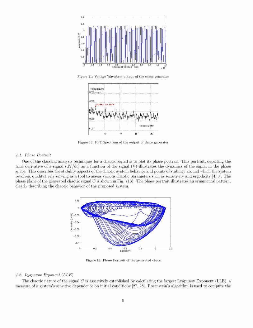
Embed Size (px)
Citation preview

Generation of Frequency Dependent Chaos using Single Transistor in 180nm CMOS
Technology
Sai Venkatesh Balasubramanian
Sree Sai Vidhya Mandhir, Mallasandra, Bengaluru-560109, Karnataka, [email protected]
Abstract
A frequency dependant chaos generator offering the twin advantages of simplicity of implementation and easy controland tunability is proposed using an iterative map based on the circle map and characterized using bifurcation diagrams.The nonlinearity of a single MOS transistor is effectively harnessed and is used to design a frequency dependant chaosgenerator using ring oscillators for the driving signals. The proposed design is implemented at the deep submicron VLSIlevel at 180nm CMOS Technology using SPICE Simulation. The generated chaos is characterized qualitatively usingwaveforms, spectra and phase portrait. Quantitative characterization using Lyapunov Exponent, Kolmogorov Entropyand Fractal Dimension ascertain the chaotic nature. Finally, the dependance of the nature of chaos generated on thepower supply and on the driving signal frequency is characterized. The simplicity of circuitry coupled with the frequencydependence and low power dissipation form the key highlights of the present work. The chaotic signal generated in thepresent work serve as a potential candidate as a carrier in secure communication systems and encryption techniques.
Keywords: Frequency Dependent Chaos, Ring Oscillator, 180nm CMOS
1. Introduction
The advancement of computing and storing power in recent years, coupled with the ability to simulate complexsystems and visualize their long-term evolution patterns has brought to the limelight, the flagship of nonlinear science,Chaos Theory [1, 2]. The principal premises of chaos theory have been determinism and an extremely sensitive depen-dence on initial conditions [3, 4, 5]. Chaos theory has found success in being able to model and study various systemsoccurring in nature such as celestial mechanics, biological systems including the electrical activity of the heart and thebrain, various chemical reactions, spread of epidemics, weather patterns and so on [4, 3, 6].
In the field of electronics and semiconductors, the introduction of a nonlinear element such as the Chua diodehave enabled considerable progress in generating a wide variety of chaotic signals, modeling classical systems suchas the Lorenz Attractor and the Rossler Attractor [5]. This generation of chaos has found immediate and significantapplication in establishing secure communication systems, which exhibit significant security enhancing properties, thanksto the sensitivity property of chaos [7, 8].
The present work purports to the definition and the generation of a new kind of chaos where the chaotic parameteris not amplitude or phase as conventionally seen, but frequency [4, 6]. The advantages of frequency dependent chaosare twofold. Firstly, it makes use of any signal naturally being decomposed into a set of frequencies. This leads toeasy implementation using a single transistor as the chaotic ‘system’, since the nonlinearity proposed in the frequencydependant chaos is the natural switching operation of the transistor [9]. Secondly, having frequency as the controlparameter makes it possible to tune the system, which enables a signal based control, a marked deviation from thesystem defined control typically seen in chaotic systems [4].
The proposed frequency dependant chaos is characterized using the iterative map and bifurcation diagrams. Then,an extremely simple circuit generating such a chaotic signal is designed and implemented in deep sub-micron VLSIlayout design at 180nm using SPICE simulations [10, 11, 12]. The essential parts of the system are ring oscillators togenerate the driving signals, and a single NMOSFET as the nonlinear element. The factor of tunability comes due tothe possibility of changing the frequency input to the single NMOSFET by altering the number of ring oscillator stages.In order to physically achieve this, a ‘programmable ring oscillator’ can be used where the number of stages actually inthe ring can be switched. The generated chaos is characterized using various standard techniques such as the LyapunovExponent, Kolmogorov Entropy and Fractal Dimension. The principal advantage of using an extremely simple circuitto generate chaos is the low value of power dissipation obtained, and this is studied using a parametric analysis [10].
It is noteworthy that generation of chaos using ring oscillators have been reported in literature [13, 14, 15, 16, 17, 18].It is seen that the basic structure of two ring oscillators being used coupled with a nonlinear circuit gives rise to chaoticbehavior. However, the design proposed in the present work differs from such results in the key aspect of frequencydependance, which can be obtained by altering the number of stages in a ring oscillator. This factor, coupled with theextremely simple circuitry and low power dissipation form the key highlights of the present work.
2. Formulation of the Frequency Dependent Chaos
The first step in the formulation of any chaotic system is an iterative map, a relation describing how a ‘chaotic’parameter of the system evolves with time with respect to a control parameter r [4]. In the present work, the chaoticparameter is frequency, rather than amplitude or phase. This offers the twin advantages of simple circuitry and tunabilityand control, as mentioned earlier.
The present work purports to designing a system that is able to generate chaos as a result of nonlinear interactionsbetween two oscillations with competing frequencies. It has been well established in literature that circle maps areideally suited to describing such systems [19, 20, 21, 22, 23]. Hence, the iterative function proposed in the present workis inspired from the standard circle map, whose iterative map is given as follows [19, 20]:
θ(i + 1) = mod(θ(i) + Ω +K
2πSin(2πθ(i)), 1) (1)
with θ being taken as modulo 1, and K and Ω being the control parameters. The standard circle map represents anarea preserving chaotic map physically seen in systems such as the kicked rotator. However, the main feature of interestin the standard circle map are the variables θ, the angular phase normalized to unity and Ω, representing an angularfrequency factor. Viewing this equation as a purely mathematical relation, as a first step, θ is written as fot where forepresents the normalized version of the angular frequency, given in the units of radians/sample, with a full scale rangeof −π to π.
Also, the time factor t is set to one, representing one sample duration, between the ith and i + 1th instants. Theadditive parameter Ω is rewritten as r where r=f2/f1 is the ratio between two normalized competing driving frequenciesf1 and f2 and is the principal control parameter for the present work. The value of K is arbitrarily set to −2π inorder to set the coefficient of the third term of the above equation to unity. Finally, the sinusoid sin(2πθ(i)) is viewedas a mathematical function representing the input and is generalised to V (2πfo(i)), or alternatively V (fo(i)), with Vrepresenting the signal waveform fed to the input of the proposed chaotic system. Using these substitutions, the aboveequation is rewritten as
fo(i+ 1) = mod(fo(i) + r − V (fo(i)), 1) (2)
It is emphasized at this stage that, by making the various modifications to the standard circle map, its physical significanceis altered considerably, and it now takes a new form represented by frequency variables and input signal dependence.In order to retain the consistency of the above equation, the various terms are normalized to π. First, the frequencyfo and the frequencies f1 and f2 are normalized to the radians/sample scale of [−π, π]. Finally, the term V (fo(i)) islimited to π, i.e. 3.14 Volts by changing the modulus function from 1 to π. It will be later seen from Fig. (3) that thevalue of 3.14 V, comprehensively encompasses the linear and saturation operating regions of the transistor, as well asforms a convenient normalizing factor yielding effective integration of the frequency and voltage terms. At this point,it is observed that the f and V terms of the above equation are merely reduced to normalized mathematical numbers.Thus, the normalized version of the above equation, with the f and V terms limited to π using a modulus function isgiven as follows:
fo(i+ 1) = mod(fo(i) +f2f1
− V (fo(i)), π) (3)
This equation is the key iterative map of the present work.Here the fo terms denote the output frequencies, whereas f1 and f2 denote the frequencies of the input (driving)
signals. V (fo) denotes the input signal waveform employed in the chaotic system. The salient features of the abovementioned iterated function are threefold, enumerated as follows:
1. The nonlinearity, provided by the modulus function represents the switching operation, which can be physicallyrealized using a transistor operating in the cutoff and saturation regions [9].
2. The control parameter r=f2/f1 is an additive parameter and determines when the system transits from order tochaos and vice versa.
2
3. The V (fo) introduces a signal dependence, thus enabling the controlling of chaos by changing the waveform used asinput. For instance, in the case of sinusoidally driven system, V (fo) becomes sin(fo(i)) which can be decomposedinto a power series containing the odd powers of (fo(i)). Thus, the signal dependance introduces nonlinearity inaddition to the system nonlinearity obtained by the switching function [9].
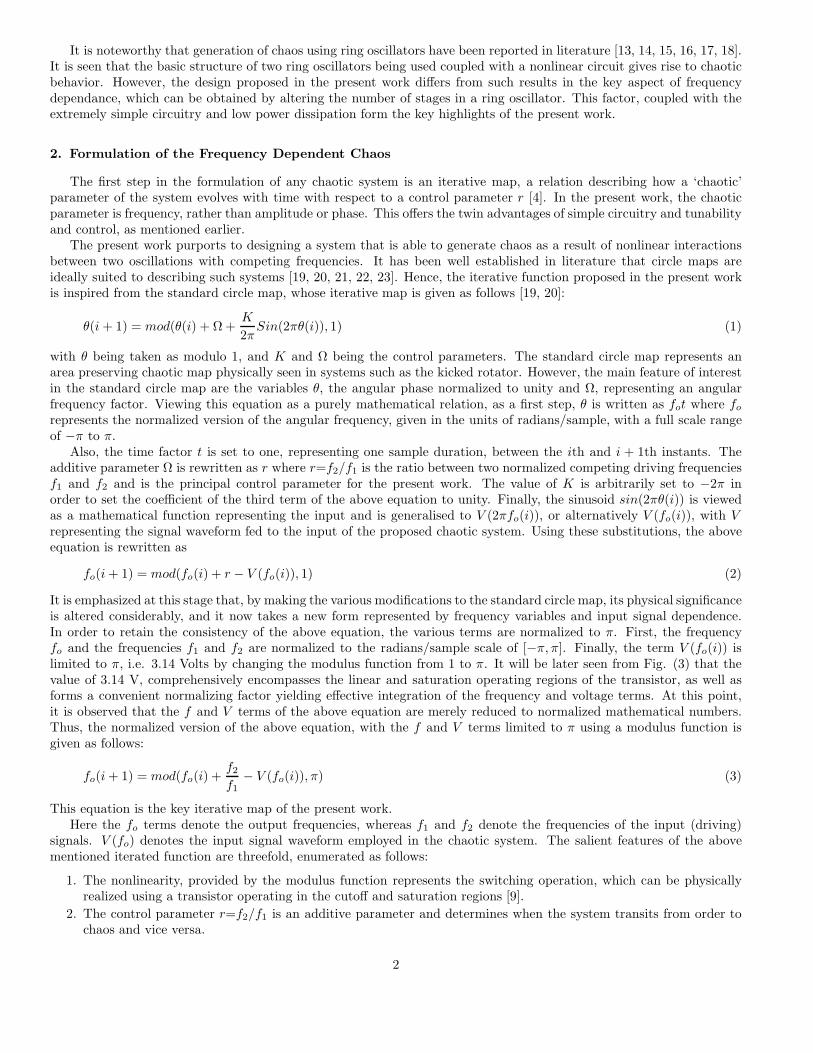
The bifurcation plot for a sinusoidal input V (fo(i))=sin(fo(i)) is given in Fig.(1).
Figure 1: Bifurcation Diagram of the chaotic system with a sinusoidal input
From the diagram, two inferences stand out:
• The bifurcation pattern repeats itself with a period of 1.
• The control values close to integers (1,2,...) and half-integers (0.5, 1.5,...) give rise to order whereas non integralratios such as 0.22 or 0.41 give rise to chaos.
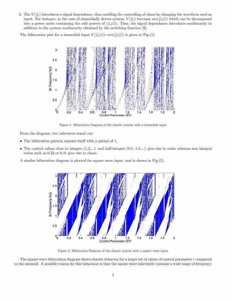
A similar bifurcation diagram is plotted for square wave input, and is shown in Fig.(2).
Figure 2: Bifurcation Diagram of the chaotic system with a square wave input
The square wave bifurcation diagram shows chaotic behavior for a larger set of values of control parameter r comparedto the sinusoid. A possible reason for this behaviour is that the square wave inherently contains a wide range of frequency
3
components, and thus allows for a more intricate interrelationship between various frequency components, as describedby the iterative map of Equation 3.
The bifurcation plots clearly describe the behavior of the proposed chaotic system for various values of the controlparameter r for typical inputs such as sinusoid and square.
3. Design and Implementation of the Chaos Generator
As highlighted in the previous section, the principal components of the proposed chaotic system are threefold - aswitching element, frequency based control parameter and driving waveform. The first component is implemented in thepresent work using a single NMOSFET and the last two components are implemented using two driving signals fed tothe gate and source terminals of the MOSFET [24, 11]. The driving signals are generated using ring oscillators. Thus,the implementation of the Ring Oscillators coupled to an NMOSFET, takes cue from Equation 3, representing the threeterms of that equation ‘in principle’ by the three above mentioned elements.
These two elements - the MOSFET and the ring oscillator are described as follows. The whole implementation iscarried out using Microwind, a deep submicron VLSI layout design software using a 180nm CMOS technology [10]. Thedevice parameters and equations employed in the Microwind implementation are obtained from BSIM4 modeling [11].
3.1. Nonlinear Behavior of the NMOSFET
The primary source of nonlinearity for the generation of the proposed chaos is a switching element, and this isimplemented using a MOSFET transistor [9, 10, 11, 12]. All the MOSFETs used in the present work are designed usinga length of 200nm and a width of 600nm. This is achieved by selecting a length-width combination of 2λ × 6λ, whereλ is the feature size, chosen in the 180nm technology to be 100nm. The nonlinearity of a MOSFET arises from twoindependent factors, described as follows.
The first factor is the the nonlinear dependence of the drain current Id on the drain voltage VD and the gate voltageVG, valid for the nonlinear point between the linear and saturation regions [25, 26].
Id =µnZCi
L
[(
VG − VFB − 2ψf −VD2
)
VD −2
3
√2ǫjsqNa
Ci
[
(VD + 2ψf)1.5
− (2ψf )1.5
]]
(4)
Here µn denotes the electron mobility, Ci the intrinsic capacitance, VFB is the flat band voltage, js is the current density,q is the charge, Na is the acceptor concentration, ψf denotes the work function, L denotes the channel length and Zdenotes the channel width, both of which are the key transistor geometry parameters [26].
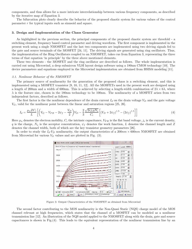
In order to study the Id-VD nonlinearity, the output characteristics of a 200nm× 600nm NMOSFET are obtainedfrom Microwind for various VG values and are plotted in Fig. (3).
Figure 3: Output Characteristics of the NMOSFET as obtained from Microwind
The second factor contributing to the MOS nonlinearity is the Non-Quasi Static (NQS) charge model of the MOSchannel relevant at high frequencies, which states that the channel of a MOSFET can be modeled as a nonlineartransmission line [12]. An illustration of the NQS model applied to the NMOSFET along with the drain, gate and sourcecapacitances is shown in Fig.(4). This leads to the equivalent representation of the nonlinear transmission line by an
4
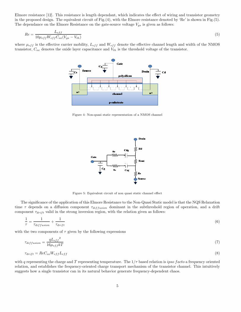
Elmore resistance [12]. This resistance is length dependant, which indicates the effect of wiring and transistor geometryin the proposed design. The equivalent circuit of Fig.(4), with the Elmore resistance denoted by ‘Re’ is shown in Fig.(5).The dependance on the Elmore Resistance on the gate-source voltage Vgs is given as follows:
Re =Leff
10µeffWeffCox(Vgs − Vth)(5)
where µeff is the effective carrier mobility, Leff and Weff denote the effective channel length and width of the NMOStransistor, Cox denotes the oxide layer capacitance and Vth is the threshold voltage of the transistor.
Figure 4: Non-quasi static representation of a NMOS channel
Figure 5: Equivalent circuit of non quasi static channel effect
The significance of the application of this Elmore Resistance to the Non-Quasi Static model is that the NQS Relaxationtime τ depends on a diffusion component τdiffusion dominant in the subthreshold region of operation, and a driftcomponent τdrift valid in the strong inversion region, with the relation given as follows:
1
τ=
1
τdiffusion+
1
τdrift(6)
with the two components of τ given by the following expressions
τdiffusion =qLeff
2
16µeffkT(7)
τdrift = ReCoxWeffLeff (8)
with q representing the charge and T representing temperature. The 1/τ based relation is ipso facto a frequency orientedrelation, and establishes the frequency-oriented charge transport mechanism of the transistor channel. This intuitivelysuggests how a single transistor can in its natural behavior generate frequency-dependent chaos.
5
3.2. Design of the Chaos Generator
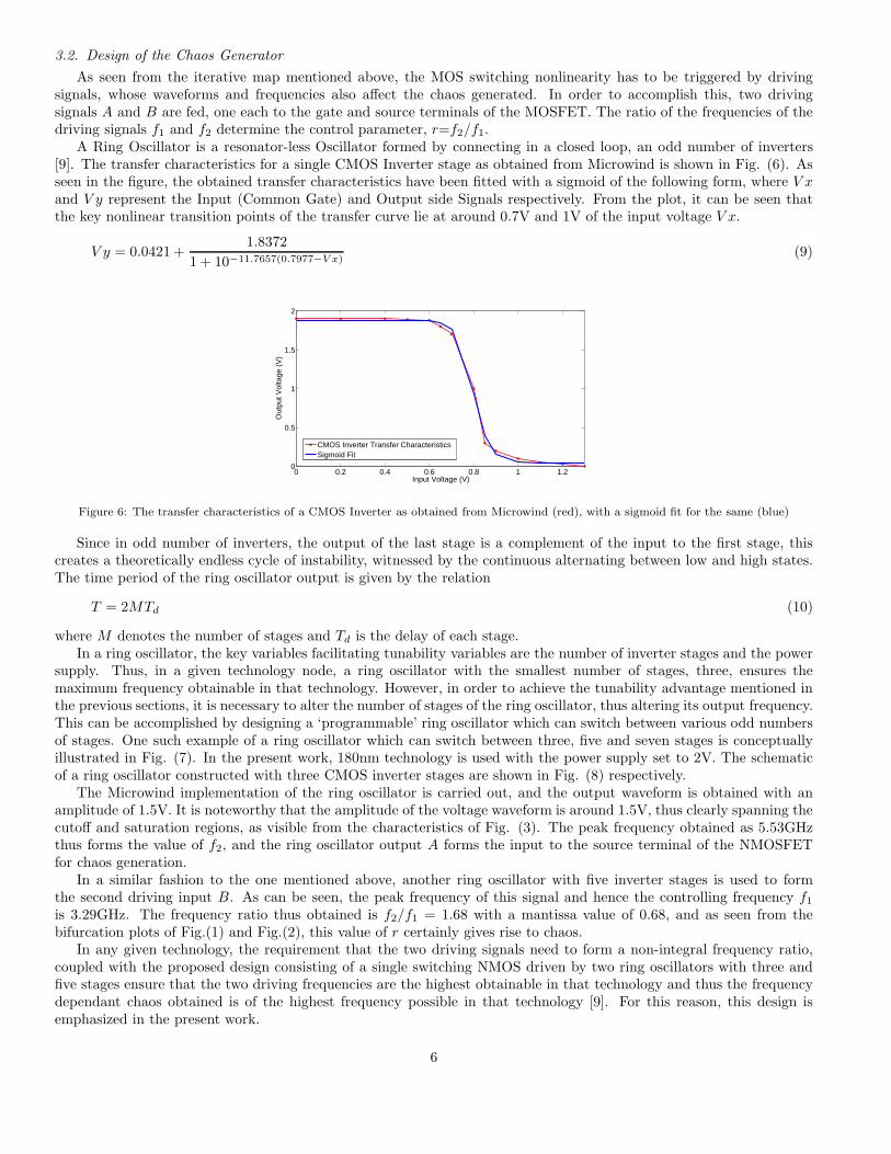
As seen from the iterative map mentioned above, the MOS switching nonlinearity has to be triggered by drivingsignals, whose waveforms and frequencies also affect the chaos generated. In order to accomplish this, two drivingsignals A and B are fed, one each to the gate and source terminals of the MOSFET. The ratio of the frequencies of thedriving signals f1 and f2 determine the control parameter, r=f2/f1.
A Ring Oscillator is a resonator-less Oscillator formed by connecting in a closed loop, an odd number of inverters[9]. The transfer characteristics for a single CMOS Inverter stage as obtained from Microwind is shown in Fig. (6). Asseen in the figure, the obtained transfer characteristics have been fitted with a sigmoid of the following form, where V xand V y represent the Input (Common Gate) and Output side Signals respectively. From the plot, it can be seen thatthe key nonlinear transition points of the transfer curve lie at around 0.7V and 1V of the input voltage V x.
V y = 0.0421 +1.8372
1 + 10−11.7657(0.7977−V x)(9)
0 0.2 0.4 0.6 0.8 1 1.20
0.5
1
1.5
2
Input Voltage (V)
Out
put V
olta
ge (
V)
CMOS Inverter Transfer CharacteristicsSigmoid Fit
Figure 6: The transfer characteristics of a CMOS Inverter as obtained from Microwind (red), with a sigmoid fit for the same (blue)
Since in odd number of inverters, the output of the last stage is a complement of the input to the first stage, thiscreates a theoretically endless cycle of instability, witnessed by the continuous alternating between low and high states.The time period of the ring oscillator output is given by the relation
T = 2MTd (10)
where M denotes the number of stages and Td is the delay of each stage.In a ring oscillator, the key variables facilitating tunability variables are the number of inverter stages and the power
supply. Thus, in a given technology node, a ring oscillator with the smallest number of stages, three, ensures themaximum frequency obtainable in that technology. However, in order to achieve the tunability advantage mentioned inthe previous sections, it is necessary to alter the number of stages of the ring oscillator, thus altering its output frequency.This can be accomplished by designing a ‘programmable’ ring oscillator which can switch between various odd numbersof stages. One such example of a ring oscillator which can switch between three, five and seven stages is conceptuallyillustrated in Fig. (7). In the present work, 180nm technology is used with the power supply set to 2V. The schematicof a ring oscillator constructed with three CMOS inverter stages are shown in Fig. (8) respectively.
The Microwind implementation of the ring oscillator is carried out, and the output waveform is obtained with anamplitude of 1.5V. It is noteworthy that the amplitude of the voltage waveform is around 1.5V, thus clearly spanning thecutoff and saturation regions, as visible from the characteristics of Fig. (3). The peak frequency obtained as 5.53GHzthus forms the value of f2, and the ring oscillator output A forms the input to the source terminal of the NMOSFETfor chaos generation.
In a similar fashion to the one mentioned above, another ring oscillator with five inverter stages is used to formthe second driving input B. As can be seen, the peak frequency of this signal and hence the controlling frequency f1is 3.29GHz. The frequency ratio thus obtained is f2/f1 = 1.68 with a mantissa value of 0.68, and as seen from thebifurcation plots of Fig.(1) and Fig.(2), this value of r certainly gives rise to chaos.
In any given technology, the requirement that the two driving signals need to form a non-integral frequency ratio,coupled with the proposed design consisting of a single switching NMOS driven by two ring oscillators with three andfive stages ensure that the two driving frequencies are the highest obtainable in that technology and thus the frequencydependant chaos obtained is of the highest frequency possible in that technology [9]. For this reason, this design isemphasized in the present work.
6
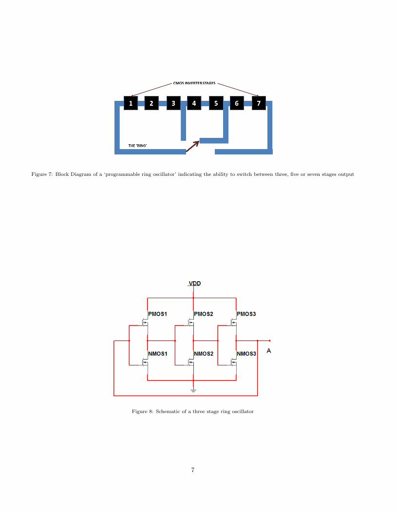
Figure 7: Block Diagram of a ‘programmable ring oscillator’ indicating the ability to switch between three, five or seven stages output
Figure 8: Schematic of a three stage ring oscillator
7
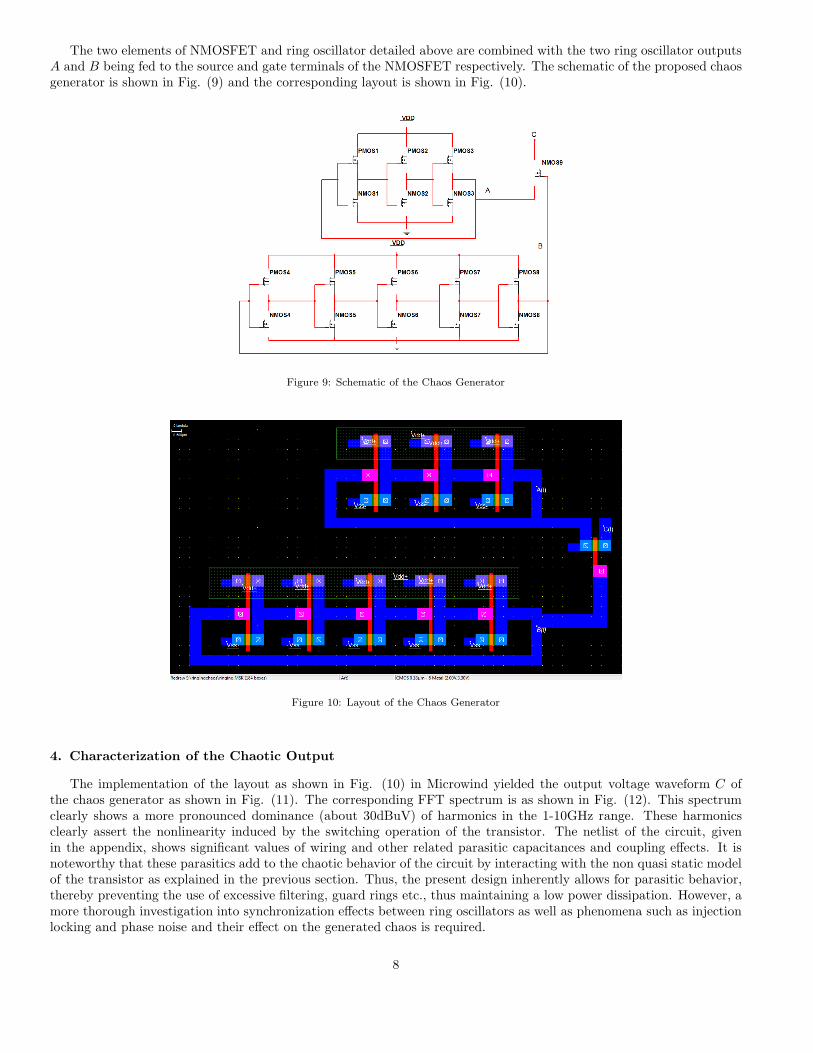
The two elements of NMOSFET and ring oscillator detailed above are combined with the two ring oscillator outputsA and B being fed to the source and gate terminals of the NMOSFET respectively. The schematic of the proposed chaosgenerator is shown in Fig. (9) and the corresponding layout is shown in Fig. (10).
Figure 9: Schematic of the Chaos Generator
Figure 10: Layout of the Chaos Generator
4. Characterization of the Chaotic Output
The implementation of the layout as shown in Fig. (10) in Microwind yielded the output voltage waveform C ofthe chaos generator as shown in Fig. (11). The corresponding FFT spectrum is as shown in Fig. (12). This spectrumclearly shows a more pronounced dominance (about 30dBuV) of harmonics in the 1-10GHz range. These harmonicsclearly assert the nonlinearity induced by the switching operation of the transistor. The netlist of the circuit, givenin the appendix, shows significant values of wiring and other related parasitic capacitances and coupling effects. It isnoteworthy that these parasitics add to the chaotic behavior of the circuit by interacting with the non quasi static modelof the transistor as explained in the previous section. Thus, the present design inherently allows for parasitic behavior,thereby preventing the use of excessive filtering, guard rings etc., thus maintaining a low power dissipation. However, amore thorough investigation into synchronization effects between ring oscillators as well as phenomena such as injectionlocking and phase noise and their effect on the generated chaos is required.
8
0 0.2 0.4 0.6 0.8 1 1.2 1.4 1.6 1.8 2
x 104
0
0.2
0.4
0.6
0.8
1
1.2
1.4
Timestep (1 timestep = 1ps)
Am
plitu
de C
(V
)Figure 11: Voltage Waveform output of the chaos generator
Figure 12: FFT Spectrum of the output of chaos generator
4.1. Phase Portrait
One of the classical analysis techniques for a chaotic signal is to plot its phase portrait. This portrait, depicting thetime derivative of a signal (dV/dt) as a function of the signal (V) illustrates the dynamics of the signal in the phasespace. This describes the stability aspects of the chaotic system behavior and points of stability around which the systemrevolves, qualitatively serving as a tool to assess various chaotic parameters such as sensitivity and ergodicity [4, 3]. Thephase plane of the generated chaotic signal C is shown in Fig. (13). The phase portrait illustrates an ornamental pattern,clearly describing the chaotic behavior of the proposed system.
0 0.2 0.4 0.6 0.8 1 1.2
−0.1
−0.08
−0.06
−0.04
−0.02
0
0.02
Signal (V)
Der
ivat
ive
(dV
/dt)
Figure 13: Phase Portrait of the generated chaos
4.2. Lyapunov Exponent (LLE)
The chaotic nature of the signal C is assertively established by calculating the largest Lyapunov Exponent (LLE), ameasure of a system’s sensitive dependence on initial conditions [27, 28]. Rosenstein’s algorithm is used to compute the
9
Lyapunov Exponents λi from the voltage waveform, where the sensitive dependence is characterized by the divergencesamples dj(i) between nearest trajectories represented by j given as follows, Cj being a normalization constant:
dj(i) = Cjeλi(iδt) (11)
The Largest Lyapunov exponent thus obtained for the signal C is 8.23, the positive value proving the fact that the signalis indeed chaotic.
4.3. Fractal Dimension (D)
The chaotic/fractal nature of the signal C is further confirmed by computing the fractal dimension, using theMinkowski Bouligand Box Counting Method [29]. In this method, various square ‘boxes’ of different sizes e are formedand for each size e, the number of boxes N(e) required to cover the entire set is computed [29]. The fractal dimensionD is then given by
D = lime→0
log(N(e))
log(e)(12)
For the output waveform of C as shown in Fig.(11), the fractal dimension is obtained as 0.661, indicating the presenceof self-similarity in the generated signal.
4.4. Kolmogorov Entropy (K2)
Finally, the worthiness of the generated signal as a potential candidate as a carrier for secure communications canbe established by ascertaining the amount of information that can be carried by the signal. This is precisely quantifiedby the Kolmogorov Entropy, a statistical measure of the uncertainty of the signal [27, 8, 1]. By assigning each of theN quantifiable states of the amplitude of C as an event i, the Kolmogorov Entropy K2 obtained depends on theirprobabilities pi according to the relation
K2 = −
N∑
i=1
pi log pi (13)
Since the chaotic output waveform is a continuously varying amplitude, a very high value of N such as 100000 is selectedas the number of quantifiable states. Thus, the presence of each of the N states is viewed as an event pi. The K2 valuethus obtained is 3.96 bits/symbol, clearly testifying to the information carrying capacity of the generated chaotic signalC.
4.5. Characterization of Power Dissipation and Effect of Noise
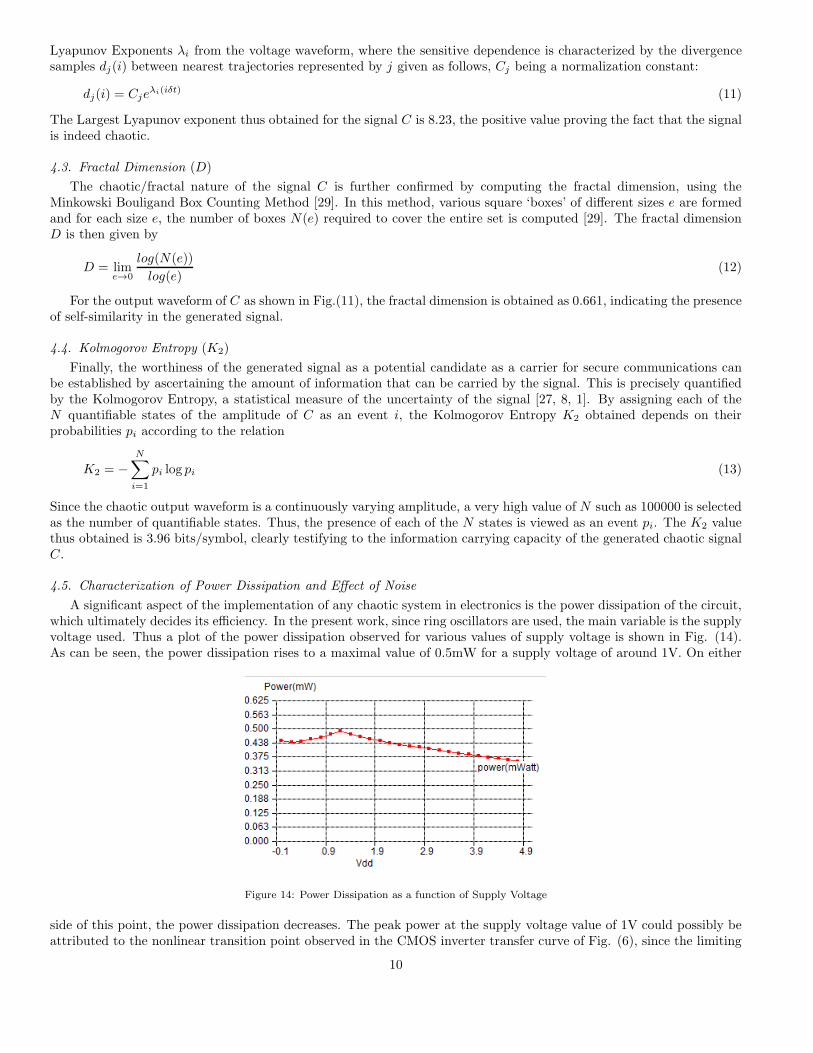
A significant aspect of the implementation of any chaotic system in electronics is the power dissipation of the circuit,which ultimately decides its efficiency. In the present work, since ring oscillators are used, the main variable is the supplyvoltage used. Thus a plot of the power dissipation observed for various values of supply voltage is shown in Fig. (14).As can be seen, the power dissipation rises to a maximal value of 0.5mW for a supply voltage of around 1V. On either
Figure 14: Power Dissipation as a function of Supply Voltage
side of this point, the power dissipation decreases. The peak power at the supply voltage value of 1V could possibly beattributed to the nonlinear transition point observed in the CMOS inverter transfer curve of Fig. (6), since the limiting
10
of supply voltage to 1V limits the peak output of the inverter to 0.9-1V, which is known as a point where the transistordraws more current, increasing power dissipation [9]. This, in turn drives the NMOSFET at the saturation region. Thevery low power dissipation obtained is owing to the extremely simple circuit used [10].
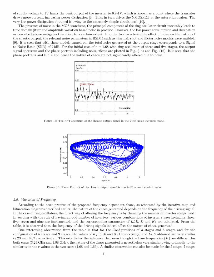
The presence of noise in the MOS transistor, the principal component of the ring oscillator circuit inevitably leads totime domain jitter and amplitude variation based noise in practice. However, the low power consumption and dissipationas described above mitigates this effect to a certain extent. In order to characterize the effect of noise on the nature ofthe chaotic output, the relevant noise parameters in BSIM4 such as thermal, shot and flicker noise models were enabled.[9]. It is seen that with these models turned on, the total noise generated at the output stage corresponds to a Signalto Noise Ratio (SNR) of 24dB. For the initial case of r = 1.68 with ring oscillators of three and five stages, the outputsignal spectrum and the phase portrait including noise effects are plotted in Fig. (15) and Fig. (16). It is seen that thephase portraits and FFTs and hence the nature of chaos are not significantly altered due to noise.
Figure 15: The FFT spectrum of the chaotic output signal in the 24dB noise included model
0 0.2 0.4 0.6 0.8 1 1.2
−0.1
−0.08
−0.06
−0.04
−0.02
0
0.02
0.04
Signal (V)
Der
ivat
ive
(dV
/dt)
Figure 16: Phase Portrait of the chaotic output signal in the 24dB noise included model
4.6. Variation of Frequency
According to the basic premise of the proposed frequency dependant chaos, as witnessed by the iterative map andbifurcation diagrams described earlier, the nature of the chaos generated depends on the frequency of the driving signal.In the case of ring oscillators, the direct way of altering the frequency is by changing the number of inverter stages used.In keeping with the rule of having an odd number of inverters, various combinations of inverter stages including three,five, seven and nine are implemented, and the corresponding parameters of LLE, D and K2 are tabulated. From thetable, it is observed that the frequency of the driving signals indeed affect the nature of chaos generated.
One interesting observation from the table is that for the Configurations of 3 stages and 5 stages and for theconfiguration of 5 stages and 9 stages, the values of K2 (3.96 and 3.91 respectively) and LLE obtained are very similar(8.23 and 8.07 respectively). This establishes the inference that even though the base frequencies (f1) are different forboth cases (3.29 GHz and 1.98 GHz), the nature of the chaos generated is nevertheless very similar owing primarily to thesimilarity in the r values in the two cases (1.68 and 1.66). A similar observation can also be made for the 5 stages-7 stages
11
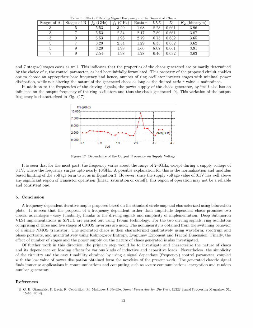
Table 1: Effect of Driving Signal Frequency on the Generated Chaos
Stages of A Stages of B f2 (GHz) f1 (GHz) Ratio r LLE D K2 (bits/sym)3 5 5.53 3.29 1.68 8.23 0.661 3.963 7 5.53 2.54 2.17 7.89 0.661 3.873 9 5.53 1.98 2.79 6.75 0.632 3.655 7 3.29 2.54 1.29 6.35 0.632 3.625 9 3.29 1.98 1.66 8.07 0.661 3.917 9 2.54 1.98 1.28 6.46 0.632 3.63
and 7 stages-9 stages cases as well. This indicates that the properties of the chaos generated are primarily determinedby the choice of r, the control parameter, as had been initially formulated. This property of the proposed circuit enablesone to choose an appropriate base frequency and hence, number of ring oscillator inverter stages with minimal powerdissipation, while not altering the nature of the generated chaos as long as the desired ratio r value is maintained.
In addition to the frequencies of the driving signals, the power supply of the chaos generator, by itself also has aninfluence on the output frequency of the ring oscillators and thus the chaos generated [9]. This variation of the outputfrequency is characterized in Fig. (17).
Figure 17: Dependance of the Output Frequency on Supply Voltage
It is seen that for the most part, the frequency varies about the range of 2-4GHz, except during a supply voltage of3.1V, where the frequency surges upto nearly 10GHz. A possible explanation for this is the normalization and modulusbased limiting of the voltage term to π, as in Equation 3. However, since the supply voltage value of 3.1V lies well aboveany significant region of transistor operation (linear, saturation or cutoff), this region of operation may not be a reliableand consistent one.
5. Conclusion
A frequency dependent iterative map is proposed based on the standard circle map and characterized using bifurcationplots. It is seen that the proposal of a frequency dependent rather than amplitude dependent chaos promises twocrucial advantages - easy tunability, thanks to the driving signals and simplicity of implementation. Deep SubmicronVLSI implementations in SPICE are carried out using 180nm technology. For the two driving signals, ring oscillatorscomprising of three and five stages of CMOS inverters are used. The nonlinearity is obtained from the switching behaviorof a single NMOS transistor. The generated chaos is then characterized qualitatively using waveform, spectrum andphase portraits, and quantitatively using Kolmogorov Entropy, Lyapunov Exponent and Fractal Dimension. Finally, theeffect of number of stages and the power supply on the nature of chaos generated is also investigated.
Of further work in this direction, the primary step would be to investigate and characterize the nature of chaosand its dependence on loading effects for various kinds of inductive and capacitive loads. Nevertheless, the simplicityof the circuitry and the easy tunability obtained by using a signal dependant (frequency) control parameter, coupledwith the low value of power dissipation obtained form the novelties of the present work. The generated chaotic signalfinds immense applications in communnications and computing such as secure communications, encryption and randomnumber generators.
References
[1] G. B. Giannakis, F. Bach, R. Cendrillon, M. Mahoney,J. Neville, Signal Processing for Big Data, IEEE Signal Processing Magazine, 31,15-16 (2014).
12

[2] M. Hilbert, How much of the global information and communication explosion is driven by more, and how much by better technology?,Wiley Journal of the Association for Information Science and Technology, 65, 856-861 (2014).
[3] M. Ausloos, M. Dirickx, The Logistic Map and the Route to Chaos: From the Beginnings to Modern Applications, (Springer, US, [2006]).[4] S. H. Strogatz, Nonlinear Dynamics and Chaos: With Applications to Physics, Biology, Chemistry, and Engineering ,(Westview Press,
Cambridge, 2008).[5] E.Bilotta and P.Pantano, A gallery of Chua attractors, (World Scientific, Singapore, 2008).[6] M. H. Jensen, P. Bak, T. Bohr, Complete Devil’s Staircase, Fractal Dimension, and Universality of Mode- Locking Structure in the
Circle Map, Phys. Rev. Lett. 50, 1637 (1983).[7] M. F. Barnsley, A. D. Sloan, Chaotic Compression, Computer Graphics World, 3 (1987).[8] K. E. Barner and G. R. Arce, Nonlinear Signal and Image Processing: Theory, Methods, and Applications, (CRC Press, U.S, 2003).[9] B. Razavi, RF Microelectronics, (Prentice Hall, US, 2011).
[10] J. P. Uyemura, Chip Design for Submicron VLSI: CMOS Layout and Simulation, (Thomson/Nelson, US, [2006]).[11] W.Liu, BSIM 4.0.0 MOSFET Model: User’s Manual (Electronics Research Laboratory,US, [2000]).[12] M.Chan, K.Hui, C.Hu, P.K.Ko, A robust and physical BSIM3 non quasi static transient and AC small signal model for circuit simulation,
IEEE Transactions on Electron Devices. 45, 834 (1998).[13] Y. Hosokawa, Y. Nishio, A. Ushida, Chaotic Circuit Using Two Simple Ring Oscillators Coupled by Diodes, Proc. NOLTA, 99, 107,
(1999).[14] Y. Hosokawa, Y. Nishio, A. Ushida, Analysis of Chaotic Phenomena in Two RC Phase Shift Oscillators Coupled by a Diode, IEICE
Transactions on Fundamentals, E84-A, 2288, (2001).[15] Y. Hosokawa, Y. Nishio, Simple Chaotic Circuit using CMOS Ring Oscillators, Int. J. Bifurcation Chaos, 14, 2513, (2004).[16] Y. Nishio, A. Ushida, Spatio-temporal chaos in simple coupled chaotic circuits, IEEE Trans. Circuits and Systems 1, 42, 678, (1995).[17] I. Cicek, G. Dundar, A hardware efficient chaotic ring oscillator based true random number generator, IEEE ICECS, 18, 430 (2011).[18] I. Cicek, G. Dundar, A chaos based integrated jitter booster circuit for true random number generators, ECCTD, 1, 8 (2013).[19] R. Gilmore and M. Lefranc, The Topology of Chaos, (Wiley,US, [2002]).[20] J. M. T. Thompson and H. B. Stewart, Nonlinear Dynamics and Chaos (Wiley,UK, [2002]).[21] V. I. Arnold, Small Denominators I. Mappings of the circumference onto itself, Am. Math. Soc. Transl, 46, 213-284 (1965).[22] M. R. Hermann, Mesure de Lebesgue et nobre de rotation (Geometry and Topology), (Springer,Germany, [1977]).[23] R. S. Mackay and C. Tresser, Some flesh on the skeleton: the bifurcation structure of bimodal maps, J. Phys. Lett., 45, L741-L746
(1984).[24] F. Balestra, Nanoscale CMOS: Innovative Materials, Modeling and Characterization (Wiley,US, [2013]).[25] M. E. Inchiosa, A. R. Bulsara, A. D. Hibbs, B. R. Whitecotton, Signal Enhancement in a Nonlinear Transfer Characteristic, Phys. Rev.
Lett. 80, 1381 (1998).[26] B. G. Streetman and S. K.Banerjee, Solid State Electronic Devices, (PHI, U.S, [2006]).[27] R. G. James, K. Burke, J. P. Crutchfield, Chaos forgets and remembers: Measuring information creation, destruction, and storage, Int.
J Bifurcation Chaos. 378, 2124 (2014).[28] M. T. Rosenstein, J. J. Collins, C. J. De Luca, A practical method for calculating largest Lyapunov exponents from small data sets,
Physica D, 65, 117, (1993).[29] P. Maragos, F. K. Sun, Measuring the fractal dimension of signals: morphological covers and iterative optimization, IEEE Trans. Signal
Processing, 41, 108-121 (1993).
13


![Tutorial_Manual Microwind 1.d[1]](https://img.pdfslide.us/doc/110x75/5540d36d4a7959f00c8b4b0f/tutorialmanual-microwind-1d1.jpg)