Embed Size (px)
Citation preview

WARNING
1SNOU150–January 2018Submit Documentation Feedback
Copyright © 2018, Texas Instruments Incorporated
General TI High Voltage Evaluation User Safety Guidelines
PrefaceSNOU150–January 2018
General TI High Voltage Evaluation User Safety Guidelines
Always follow TI’s set-up and application instructions, including the use of all interface components withinthe recommended electrical rated voltage and power limits. Always use electrical safety precautions tohelp ensure your personal safety and the safety of those working around you. Contact TI’s ProductInformation Center at http://support/ti./com for further information.
NOTE: Save all warnings and instructions for future reference.
Failure to follow warnings and instructions may result in personal injury, propertydamage, or death due to electrical shock and/or burn hazards.
The term TI HV EVM refers to an electronic device typically provided as an open framed, unenclosed PCB(printed circuit board)assembly. It is intended strictly for use in development laboratory environments,solely for qualified professional users having training, expertise, and knowledge of electrical safety risks indevelopment and application of high-voltage electrical circuits. Any other use or application is strictlyprohibited by Texas Instruments. If you are not suitably qualified, you should immediately stop from furtheruse of the HV EVM.• Work Area Safety:
– Maintain a clean and orderly work area.– Qualified observer(s) must be present anytime circuits are energized.– Effective barriers and signage must be present in the area where the TI HV EVM and its interface
electronics are energized; indicating operation of accessible high voltages may be present for thepurpose of protecting inadvertent access.
– All interface circuits, power supplies, evaluation modules, instruments, meters, scopes, and otherrelated apparatus used in a development environment exceeding 50 VRMS/75 VDC must beelectrically located within a protected Emergency Power Off (EPO) power strip.
– Use a stable and non-conductive work surface.– Use adequately insulated clamps and wires to attach measurement probes and instruments. No
freehand testing whenever possible.• Electrical Safety:
– As a precautionary measure, it is always a good engineering practice to assume that the entireEVM may have fully accessible and active high voltages.
– De-energize the TI HV EVM and all its inputs, outputs, and electrical loads before performing anyelectrical or other diagnostic measurements. Confirm that TI HV EVM power has been safely de-energized.
– After confirming the EVM is de-energized, proceed with the required electrical circuit configurations,wiring, measurement equipment hook-ups, and other application needs while still assuming theEVM circuit and measuring instruments are electrically live.
– When EVM readiness is complete, energize the EVM as intended.
!
Safety and Precautions www.ti.com
2 SNOU150–January 2018Submit Documentation Feedback
Copyright © 2018, Texas Instruments Incorporated
General TI High Voltage Evaluation User Safety Guidelines
WARNINGWhile the EVM is energized, never touch the EVM or its electricalcircuits as they could be at high voltages capable of causingelectrical shock hazard.
• Personal Safety:– Wear personal protective equipment like latex gloves and safety glasses with side shields, or
protect the EVM from accidental touch in an adequate translucent plastic box with interlocks.• Limitation for Safe Use:
– EVMs are not to be used as all or part of a production unit.
Safety and PrecautionsThe EVM is designed for professionals who have received the appropriate technical training and isdesigned to operate from an AC power supply or a high-voltage DC supply. Read this user guide and thesafety-related documents that come with the EVM package before operating this EVM.
CAUTION
Do not leave the EVM powered when unattended.
WARNING
Hot surface! Contact may cause burns. Do not touch!
WARNING
High Voltage! Electric shock is possible when connecting board tolive wire. Board should be handled with care by a professional.For safety, use of isolated test equipment with overvoltage andovercurrent protection is highly recommended.
3SNOU150–January 2018Submit Documentation Feedback
Copyright © 2018, Texas Instruments Incorporated
Using the LMG1020-EVM Nano-second LiDAR EVM
User's GuideSNOU150–January 2018
Using the LMG1020-EVM Nano-second LiDAR EVM
Contents1 Introduction ................................................................................................................... 42 Description.................................................................................................................... 43 Electrical Performance Specifications..................................................................................... 54 EVM Schematic .............................................................................................................. 65 EVM Kit Contents ............................................................................................................ 76 Test Setup .................................................................................................................... 77 Test Procedure ............................................................................................................. 108 Performance Data and Typical Characteristics......................................................................... 119 EVM Assembly Drawing and PCB Layout .............................................................................. 1210 Bill of Materials ............................................................................................................. 13
List of Figures
1 LiDAR Power Stage with LMG1020 ....................................................................................... 42 Power Stage Schematic (DNP = Do Not Place, Not Present On Board) ............................................ 63 Recommended Connection Points and Feature Description .......................................................... 74 Recommended Use for Ground Spring Clip Test Points ............................................................... 85 Visual and Description of Ground Spring Clip Test Points ............................................................. 96 90ns Pulse from Function Generator Yielding 15ns Pulse on the Gate ........................................... 117 90ns Pulse from Function Generator Yielding 15ns Pulse on the Gate ............................................ 118 84ns Pulse from Function Generator Yielding 1.5ns Pulse on the Gate ........................................... 119 1.2ns Gate Pulse Yielding 1.5ns 30V into 1Ω Pulse (500MHz Scope) ............................................. 1110 LMG1210-HB-EVM Top Layer and Components ...................................................................... 1211 LMG1210-HB-EVM Bottom Layer and Components .................................................................. 12
List of Tables
1 LMG1020-EVM Electrical Performance Specifications ................................................................. 52 Test Point Functional Description ......................................................................................... 83 List of Terminals ............................................................................................................. 94 LMG1210-HB-EVM List of Materials..................................................................................... 13

Introduction www.ti.com
4 SNOU150–January 2018Submit Documentation Feedback
Copyright © 2018, Texas Instruments Incorporated
Using the LMG1020-EVM Nano-second LiDAR EVM
1 IntroductionThe LMG1020-HB-EVM is designed to evaluate the LMG1020 Nano-second low-side driver for GaN FETsThis EVM consists of one Gallium Nitride (GaN) eFET driven by one LMG1020 and with the sourceconnected to a resistive load emulating a laser diode for LiDAR (Light Detection And Ranging)applications.
The guide shows a circuit and the list of materials describing how to power the board up and how to setthe board up for a certain regulation voltage. The EVM board is designed to accelerate the evaluation ofthe LMG1020.
This board is not intended to be used as a standalone product but it intended to evaluate the switchingperformance of LMG1020.
This EVM guide describes correct operation and measurement of the EVM, as well as the EVMconstruction and typical performance.
2 DescriptionThe LMG1020-EVM is a small, easy-to-use power stage with integrated resistive load. It takes a short-pulse input that can either be buffered (and shorten further), or passed directly to the power stage.
The input pulse is signal is used to pulse the current through the load, to achieve 1-2ns wide currentpulses, which are the state-of-the-art target for LiDAR systems.
The EVM features a LMG1020 low side nano-second driver, driving a single EPC2039 FET referenced toground and with the drain connected to the resistive load.
The load is split between two current loops to reduce the effective inductance. The board has larger padson which a laser diode of choice can be mounted.
Figure 1. LiDAR Power Stage with LMG1020
The power stage can deliver up to 40 A of current to the load at duty cycles ~0.1% and frequencies up to1-2MHz. It includes adequate thermal management (if required, case temperature should be monitoredand adequate airflow should be ensured).
2.1 Typical ApplicationsThe LMG1020 is suited for use in high frequency which may require nano-second long minimum pulsewidth. The extremely short pulse capability and short propagation delay, allow for state-of-the-artsolutions.
Typical applications include:• LiDAR power stage• Wireless power• VHF converters

www.ti.com Description
5SNOU150–January 2018Submit Documentation Feedback
Copyright © 2018, Texas Instruments Incorporated
Using the LMG1020-EVM Nano-second LiDAR EVM
CAUTIONHigh-voltage levels are present on the evaluation module whenever it isenergized. Proper precautions must be taken when working with the EVM.
2.2 FeaturesThe LMG1020 has the following features and specifications:• Single low-side ultra-fast driver for 5V drive GaN and silicon FETs• Single 5V supply• Schmitt-trigger type CMOS inputs for robustness• 2.5 ns typical, 4.5 ns max propagation delay• 210 ps typical rise/fall time• UVLO and over-temperature protection• Minimum footprint 2x3 ball WCSP minimizes gate loop inductance and maximizes power density
3 Electrical Performance Specifications
(1) Determined by the thermal dissipation; depending on the magnitude of the current pulse and duty cycle.
Table 1. LMG1020-EVM Electrical Performance Specifications
PARAMETER TEST CONDITIONS MIN TYP MAX UNITInput and Output CharacteristicsInput Voltage 0 75 VDCInput current 0 0.1 ABias voltage Iout,MAX = 100 mA 6 18 VDCSystem CharacteristicsSwitching frequency 0.1 1 50 (1) MHz

EVM Schematic www.ti.com
6 SNOU150–January 2018Submit Documentation Feedback
Copyright © 2018, Texas Instruments Incorporated
Using the LMG1020-EVM Nano-second LiDAR EVM
4 EVM Schematic
Figure 2. Power Stage Schematic (DNP = Do Not Place, Not Present On Board)
www.ti.com EVM Kit Contents
7SNOU150–January 2018Submit Documentation Feedback
Copyright © 2018, Texas Instruments Incorporated
Using the LMG1020-EVM Nano-second LiDAR EVM
5 EVM Kit ContentsThe kit contains the following:• Using the LMG1020-EVM (this user's guide)• Safety instructions• LMG1020-EVM EVM PCB assembly
6 Test Setup
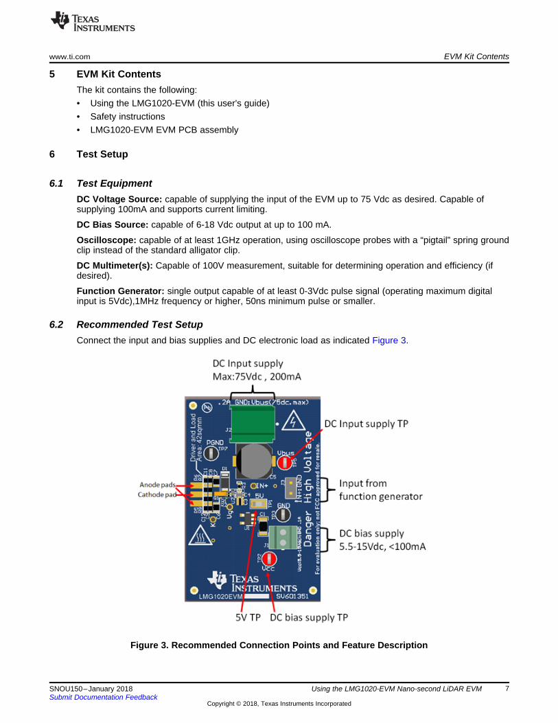
6.1 Test EquipmentDC Voltage Source: capable of supplying the input of the EVM up to 75 Vdc as desired. Capable ofsupplying 100mA and supports current limiting.
DC Bias Source: capable of 6-18 Vdc output at up to 100 mA.
Oscilloscope: capable of at least 1GHz operation, using oscilloscope probes with a “pigtail” spring groundclip instead of the standard alligator clip.
DC Multimeter(s): Capable of 100V measurement, suitable for determining operation and efficiency (ifdesired).
Function Generator: single output capable of at least 0-3Vdc pulse signal (operating maximum digitalinput is 5Vdc),1MHz frequency or higher, 50ns minimum pulse or smaller.
6.2 Recommended Test SetupConnect the input and bias supplies and DC electronic load as indicated Figure 3.
Figure 3. Recommended Connection Points and Feature Description
Test Setup www.ti.com
8 SNOU150–January 2018Submit Documentation Feedback
Copyright © 2018, Texas Instruments Incorporated
Using the LMG1020-EVM Nano-second LiDAR EVM
WARNINGHigh voltages that may cause injury exist on this evaluationmodule (EVM). Please ensure all safety procedures are followedwhen working on this EVM. Never leave a powered EVMunattended.
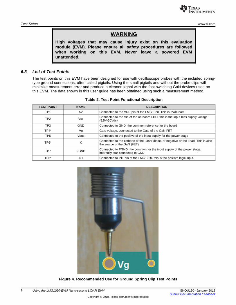
6.3 List of Test PointsThe test points on this EVM have been designed for use with oscilloscope probes with the included spring-type ground connections, often called pigtails. Using the small pigtails and without the probe clips willminimize measurement error and produce a cleaner signal with the fast switching GaN devices used onthis EVM. The data shown in this user guide has been obtained using such a measurement method.
Table 2. Test Point Functional Description
TEST POINT NAME DESCRIPTIONTP1 5V Connected to the VDD pin of the LMG1020. This is 5Vdc nom
TP2 Vcc Connected to the Vin of the on board LDO, this is the input bias supply voltage(5.5V-30Vdc)
TP3 GND Connected to GND, the common reference for the boardTP4* Vg Gate voltage, connected to the Gate of the GaN FETTP5 Vbus Connected to the positive of the input supply for the power stage
TP6* K Connected to the cathode of the Laser diode, or negative or the Load. This is alsothe source of the GaN )FET)
TP7 PGND Connected to PGND, the common for the input supply of the power stage,internally star-connected to GND
TP8* IN+ Connected to IN+ pin of the LMG1020, this is the positive logic input.
Figure 4. Recommended Use for Ground Spring Clip Test Points

www.ti.com Test Setup
9SNOU150–January 2018Submit Documentation Feedback
Copyright © 2018, Texas Instruments Incorporated
Using the LMG1020-EVM Nano-second LiDAR EVM
Figure 5. Visual and Description of Ground Spring Clip Test Points
6.4 List of Terminals
Table 3. List of Terminals
TERMINALS NAME DESCRIPTIONJ1 DC Bias Supply (Vcc) Bias supply connection terminals (5.5-30 Vdc, 0.1A)J2 DC Input Supply (Vbus) Input voltage connection terminals (MAX: 75 Vdc, 0.2A)
J3 Input signal Connector for function generator input, connected through a buffer to thepositive input of the LMG1020
Test Procedure www.ti.com
10 SNOU150–January 2018Submit Documentation Feedback
Copyright © 2018, Texas Instruments Incorporated
Using the LMG1020-EVM Nano-second LiDAR EVM
7 Test Procedure
WARNINGThere are very high voltages present on the EVM. Somecomponents reach temperatures above 50°C. Precautions must betaken when handling the board.
7.1 Nanosecond Pulse MeasurementsThe following procedure is used to obtain and measure nano-second(s) pulse at the output:1. Connect the input(J2) and bias supplies(J1) as shown in Figure 3, but do not power them on yet.2. Power up the DC bias supply (J1) maintaining it in the 5.5V to 15V range and setting the current limit
to 0.1A.3. Connect the function generator and apply the following settings:
• Frequency to 100kHz• Signal range 0-3V• Pulse width 100ns• Enable the output
4. Power up the input supply(J2) (as shown in Figure 3) and set to the desired input voltage, but nohigher than 75Vdc. Set the current limit to 0.2A. a. It is recommended to begin measurements at lowervoltage, such as 10V to ensure the correct waveforms are being captured.
5. Tune the length of the pulse on the function generator, so that the Cathode voltage pulse is reduced tothe desired width, this will be close to 1-2ns. Notice that if the on-board resistive load is being used,the rising edge of the pulse is given by the RC constant of the load in series with the COSS of theFET.
6. Perform the desired measurements
7.2 Shutdown ProcedureOnce the desired measurements have been completed, shut down the EVM by following these steps:1. Turn off the DC input power supply(J2)2. Disable the function generator3. Disable the bias supply(J1)
7.2.1 Components rating and DNPs• All input capacitors are 100V rates• The EPC2019 FET is 200V rated to withstand inductive voltage spikes• The digital input buffer is placed to generate clean input signals on the board and to shorten the input
pulse. To bypass it, the DNP resistor R3 has to be placed and resistor R10 has to be removed.
www.ti.com Performance Data and Typical Characteristics
11SNOU150–January 2018Submit Documentation Feedback
Copyright © 2018, Texas Instruments Incorporated
Using the LMG1020-EVM Nano-second LiDAR EVM
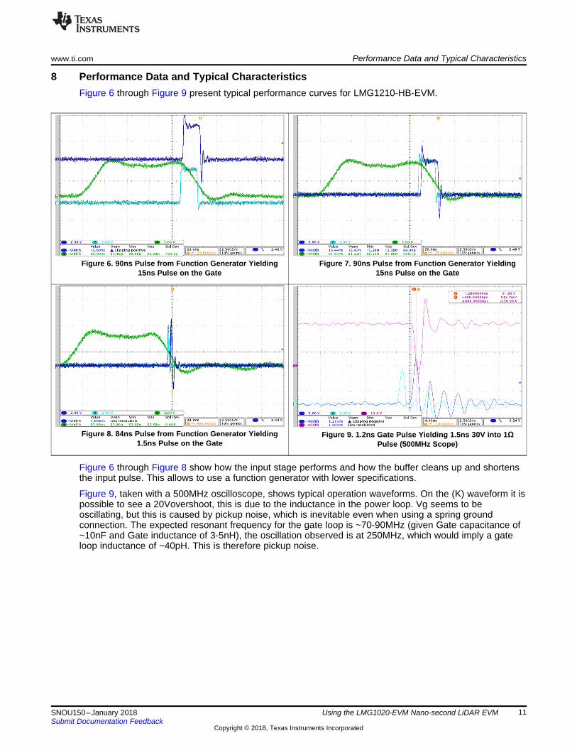
8 Performance Data and Typical CharacteristicsFigure 6 through Figure 9 present typical performance curves for LMG1210-HB-EVM.
Figure 6. 90ns Pulse from Function Generator Yielding15ns Pulse on the Gate
Figure 7. 90ns Pulse from Function Generator Yielding15ns Pulse on the Gate
Figure 8. 84ns Pulse from Function Generator Yielding1.5ns Pulse on the Gate
Figure 9. 1.2ns Gate Pulse Yielding 1.5ns 30V into 1ΩPulse (500MHz Scope)
Figure 6 through Figure 8 show how the input stage performs and how the buffer cleans up and shortensthe input pulse. This allows to use a function generator with lower specifications.
Figure 9, taken with a 500MHz oscilloscope, shows typical operation waveforms. On the (K) waveform it ispossible to see a 20Vovershoot, this is due to the inductance in the power loop. Vg seems to beoscillating, but this is caused by pickup noise, which is inevitable even when using a spring groundconnection. The expected resonant frequency for the gate loop is ~70-90MHz (given Gate capacitance of~10nF and Gate inductance of 3-5nH), the oscillation observed is at 250MHz, which would imply a gateloop inductance of ~40pH. This is therefore pickup noise.

EVM Assembly Drawing and PCB Layout www.ti.com
12 SNOU150–January 2018Submit Documentation Feedback
Copyright © 2018, Texas Instruments Incorporated
Using the LMG1020-EVM Nano-second LiDAR EVM
9 EVM Assembly Drawing and PCB Layout
Figure 10. LMG1210-HB-EVM Top Layer and Components
Figure 11. LMG1210-HB-EVM Bottom Layer and Components

www.ti.com Bill of Materials
13SNOU150–January 2018Submit Documentation Feedback
Copyright © 2018, Texas Instruments Incorporated
Using the LMG1020-EVM Nano-second LiDAR EVM
10 Bill of Materials
Table 4. LMG1210-HB-EVM List of Materials
QUANTITY DESIGNATOR DESCRIPTION PART NUMBER1 C1 CAP, CERM, 10 µF, 25 V, +/- 10%, X7R, 1206 8850122080691 C3 CAP, CERM, 1 µF, 10 V, +/- 20%, X5R, 0306 LWK107BJ105MV1 C4 Feedthru Capacitor, 0.47uF, 6.3V, SMD YFF18PW0J474M2 C6, C7 CAP, CERM, 0.01 µF, 100 V, +/- 1%, C0G/NP0, 0805 C0805C103F1GACTU
4 C8, C9, C11,C12 CAP, CERM, 0.1 µF, 100 V, +/- 10%, X7R, 0603 GRM188R72A104KA35D
1 C10 CAP, CERM, 0.1uF, 25V, +/-10%, X7R, 0603 GRM188R71E104KA01D1 C13 CAP, CERM, 20 pF, 50 V, +/- 5%, C0G/NP0, 0402 GRM1555C1H200JA01D1 D1 Diode, Schottky, 100 V, 2 A, PowerDI123 DFLS2100-7
3 FID1, FID2,FID3 Fiducial mark. There is nothing to buy or mount. Fiducial
4 H1, H2, H3, H4 Bumpon, Hemisphere, 0.44 X 0.20, Clear SJ-5303 (CLEAR)1 J1 Terminal Block, 2.54mm, 2x1, Brass, TH OSTVN02A1501 J2 Terminal Block, 2x1, 5.08mm, TH 282841-21 J3 Header, 100mil, 2x1, Gold, TH HTSW-102-07-G-S1 Q1 MOSFET, N-CH, 200 V, 8.5 A, 2.766x0.68mm EPC20192 R1, R2 RES, 0, 5%, 0.05 W, 0201 ERJ-1GE0R00C4 R5, R6, R7, R8 RES, 4.02, 0.5%, 0.1 W, 0603 RT0603DRE074R02L1 R9 RES, 4.99 k, 1%, 0.1 W, 0603 CR0603-FX-4991ELF1 R10 RES, 0, 5%, 0.063 W, 0402 CRCW04020000Z0ED1 TP1 Test Point, Miniature, SMT 50151 TP2 Test Point, Compact, Red, TH 50051 TP3 Test Point, Compact, Black, TH 50061 TP5 Test Point, Compact, Red, TH 50051 TP7 Test Point, Compact, Black, TH 5006
1 U1 150-mA, 30-V, 1-uA IQ Voltage Regulators with Enable, DBV0005A(SOT-5) TPS70950DBVR
1 U2 High Speed Gate Driver in WCSP Package, YFF XLMG10201 U3 Single 2-Input Positive-AND Gate, DCK0005A (SOT-5) SN74LVC1G08DCKR

STANDARD TERMS FOR EVALUATION MODULES1. Delivery: TI delivers TI evaluation boards, kits, or modules, including any accompanying demonstration software, components, and/or
documentation which may be provided together or separately (collectively, an “EVM” or “EVMs”) to the User (“User”) in accordancewith the terms set forth herein. User's acceptance of the EVM is expressly subject to the following terms.1.1 EVMs are intended solely for product or software developers for use in a research and development setting to facilitate feasibility
evaluation, experimentation, or scientific analysis of TI semiconductors products. EVMs have no direct function and are notfinished products. EVMs shall not be directly or indirectly assembled as a part or subassembly in any finished product. Forclarification, any software or software tools provided with the EVM (“Software”) shall not be subject to the terms and conditionsset forth herein but rather shall be subject to the applicable terms that accompany such Software
1.2 EVMs are not intended for consumer or household use. EVMs may not be sold, sublicensed, leased, rented, loaned, assigned,or otherwise distributed for commercial purposes by Users, in whole or in part, or used in any finished product or productionsystem.
2 Limited Warranty and Related Remedies/Disclaimers:2.1 These terms do not apply to Software. The warranty, if any, for Software is covered in the applicable Software License
Agreement.2.2 TI warrants that the TI EVM will conform to TI's published specifications for ninety (90) days after the date TI delivers such EVM
to User. Notwithstanding the foregoing, TI shall not be liable for a nonconforming EVM if (a) the nonconformity was caused byneglect, misuse or mistreatment by an entity other than TI, including improper installation or testing, or for any EVMs that havebeen altered or modified in any way by an entity other than TI, (b) the nonconformity resulted from User's design, specificationsor instructions for such EVMs or improper system design, or (c) User has not paid on time. Testing and other quality controltechniques are used to the extent TI deems necessary. TI does not test all parameters of each EVM.User's claims against TI under this Section 2 are void if User fails to notify TI of any apparent defects in the EVMs within ten (10)business days after delivery, or of any hidden defects with ten (10) business days after the defect has been detected.
2.3 TI's sole liability shall be at its option to repair or replace EVMs that fail to conform to the warranty set forth above, or creditUser's account for such EVM. TI's liability under this warranty shall be limited to EVMs that are returned during the warrantyperiod to the address designated by TI and that are determined by TI not to conform to such warranty. If TI elects to repair orreplace such EVM, TI shall have a reasonable time to repair such EVM or provide replacements. Repaired EVMs shall bewarranted for the remainder of the original warranty period. Replaced EVMs shall be warranted for a new full ninety (90) daywarranty period.
3 Regulatory Notices:3.1 United States
3.1.1 Notice applicable to EVMs not FCC-Approved:FCC NOTICE: This kit is designed to allow product developers to evaluate electronic components, circuitry, or softwareassociated with the kit to determine whether to incorporate such items in a finished product and software developers to writesoftware applications for use with the end product. This kit is not a finished product and when assembled may not be resold orotherwise marketed unless all required FCC equipment authorizations are first obtained. Operation is subject to the conditionthat this product not cause harmful interference to licensed radio stations and that this product accept harmful interference.Unless the assembled kit is designed to operate under part 15, part 18 or part 95 of this chapter, the operator of the kit mustoperate under the authority of an FCC license holder or must secure an experimental authorization under part 5 of this chapter.3.1.2 For EVMs annotated as FCC – FEDERAL COMMUNICATIONS COMMISSION Part 15 Compliant:
CAUTIONThis device complies with part 15 of the FCC Rules. Operation is subject to the following two conditions: (1) This device may notcause harmful interference, and (2) this device must accept any interference received, including interference that may causeundesired operation.Changes or modifications not expressly approved by the party responsible for compliance could void the user's authority tooperate the equipment.
FCC Interference Statement for Class A EVM devicesNOTE: This equipment has been tested and found to comply with the limits for a Class A digital device, pursuant to part 15 ofthe FCC Rules. These limits are designed to provide reasonable protection against harmful interference when the equipment isoperated in a commercial environment. This equipment generates, uses, and can radiate radio frequency energy and, if notinstalled and used in accordance with the instruction manual, may cause harmful interference to radio communications.Operation of this equipment in a residential area is likely to cause harmful interference in which case the user will be required tocorrect the interference at his own expense.
FCC Interference Statement for Class B EVM devicesNOTE: This equipment has been tested and found to comply with the limits for a Class B digital device, pursuant to part 15 ofthe FCC Rules. These limits are designed to provide reasonable protection against harmful interference in a residentialinstallation. This equipment generates, uses and can radiate radio frequency energy and, if not installed and used in accordancewith the instructions, may cause harmful interference to radio communications. However, there is no guarantee that interferencewill not occur in a particular installation. If this equipment does cause harmful interference to radio or television reception, whichcan be determined by turning the equipment off and on, the user is encouraged to try to correct the interference by one or moreof the following measures:
• Reorient or relocate the receiving antenna.• Increase the separation between the equipment and receiver.• Connect the equipment into an outlet on a circuit different from that to which the receiver is connected.• Consult the dealer or an experienced radio/TV technician for help.
3.2 Canada3.2.1 For EVMs issued with an Industry Canada Certificate of Conformance to RSS-210 or RSS-247
Concerning EVMs Including Radio Transmitters:This device complies with Industry Canada license-exempt RSSs. Operation is subject to the following two conditions:(1) this device may not cause interference, and (2) this device must accept any interference, including interference that maycause undesired operation of the device.
Concernant les EVMs avec appareils radio:Le présent appareil est conforme aux CNR d'Industrie Canada applicables aux appareils radio exempts de licence. L'exploitationest autorisée aux deux conditions suivantes: (1) l'appareil ne doit pas produire de brouillage, et (2) l'utilisateur de l'appareil doitaccepter tout brouillage radioélectrique subi, même si le brouillage est susceptible d'en compromettre le fonctionnement.
Concerning EVMs Including Detachable Antennas:Under Industry Canada regulations, this radio transmitter may only operate using an antenna of a type and maximum (or lesser)gain approved for the transmitter by Industry Canada. To reduce potential radio interference to other users, the antenna typeand its gain should be so chosen that the equivalent isotropically radiated power (e.i.r.p.) is not more than that necessary forsuccessful communication. This radio transmitter has been approved by Industry Canada to operate with the antenna typeslisted in the user guide with the maximum permissible gain and required antenna impedance for each antenna type indicated.Antenna types not included in this list, having a gain greater than the maximum gain indicated for that type, are strictly prohibitedfor use with this device.
Concernant les EVMs avec antennes détachablesConformément à la réglementation d'Industrie Canada, le présent émetteur radio peut fonctionner avec une antenne d'un type etd'un gain maximal (ou inférieur) approuvé pour l'émetteur par Industrie Canada. Dans le but de réduire les risques de brouillageradioélectrique à l'intention des autres utilisateurs, il faut choisir le type d'antenne et son gain de sorte que la puissance isotroperayonnée équivalente (p.i.r.e.) ne dépasse pas l'intensité nécessaire à l'établissement d'une communication satisfaisante. Leprésent émetteur radio a été approuvé par Industrie Canada pour fonctionner avec les types d'antenne énumérés dans lemanuel d’usage et ayant un gain admissible maximal et l'impédance requise pour chaque type d'antenne. Les types d'antennenon inclus dans cette liste, ou dont le gain est supérieur au gain maximal indiqué, sont strictement interdits pour l'exploitation del'émetteur
3.3 Japan3.3.1 Notice for EVMs delivered in Japan: Please see http://www.tij.co.jp/lsds/ti_ja/general/eStore/notice_01.page 日本国内に
輸入される評価用キット、ボードについては、次のところをご覧ください。http://www.tij.co.jp/lsds/ti_ja/general/eStore/notice_01.page
3.3.2 Notice for Users of EVMs Considered “Radio Frequency Products” in Japan: EVMs entering Japan may not be certifiedby TI as conforming to Technical Regulations of Radio Law of Japan.
If User uses EVMs in Japan, not certified to Technical Regulations of Radio Law of Japan, User is required to follow theinstructions set forth by Radio Law of Japan, which includes, but is not limited to, the instructions below with respect to EVMs(which for the avoidance of doubt are stated strictly for convenience and should be verified by User):1. Use EVMs in a shielded room or any other test facility as defined in the notification #173 issued by Ministry of Internal
Affairs and Communications on March 28, 2006, based on Sub-section 1.1 of Article 6 of the Ministry’s Rule forEnforcement of Radio Law of Japan,
2. Use EVMs only after User obtains the license of Test Radio Station as provided in Radio Law of Japan with respect toEVMs, or
3. Use of EVMs only after User obtains the Technical Regulations Conformity Certification as provided in Radio Law of Japanwith respect to EVMs. Also, do not transfer EVMs, unless User gives the same notice above to the transferee. Please notethat if User does not follow the instructions above, User will be subject to penalties of Radio Law of Japan.

【無線電波を送信する製品の開発キットをお使いになる際の注意事項】 開発キットの中には技術基準適合証明を受けていないものがあります。 技術適合証明を受けていないもののご使用に際しては、電波法遵守のため、以下のいずれかの措置を取っていただく必要がありますのでご注意ください。1. 電波法施行規則第6条第1項第1号に基づく平成18年3月28日総務省告示第173号で定められた電波暗室等の試験設備でご使用
いただく。2. 実験局の免許を取得後ご使用いただく。3. 技術基準適合証明を取得後ご使用いただく。
なお、本製品は、上記の「ご使用にあたっての注意」を譲渡先、移転先に通知しない限り、譲渡、移転できないものとします。上記を遵守頂けない場合は、電波法の罰則が適用される可能性があることをご留意ください。 日本テキサス・イ
ンスツルメンツ株式会社東京都新宿区西新宿6丁目24番1号西新宿三井ビル
3.3.3 Notice for EVMs for Power Line Communication: Please see http://www.tij.co.jp/lsds/ti_ja/general/eStore/notice_02.page電力線搬送波通信についての開発キットをお使いになる際の注意事項については、次のところをご覧ください。http://www.tij.co.jp/lsds/ti_ja/general/eStore/notice_02.page
3.4 European Union3.4.1 For EVMs subject to EU Directive 2014/30/EU (Electromagnetic Compatibility Directive):
This is a class A product intended for use in environments other than domestic environments that are connected to alow-voltage power-supply network that supplies buildings used for domestic purposes. In a domestic environment thisproduct may cause radio interference in which case the user may be required to take adequate measures.
4 EVM Use Restrictions and Warnings:4.1 EVMS ARE NOT FOR USE IN FUNCTIONAL SAFETY AND/OR SAFETY CRITICAL EVALUATIONS, INCLUDING BUT NOT
LIMITED TO EVALUATIONS OF LIFE SUPPORT APPLICATIONS.4.2 User must read and apply the user guide and other available documentation provided by TI regarding the EVM prior to handling
or using the EVM, including without limitation any warning or restriction notices. The notices contain important safety informationrelated to, for example, temperatures and voltages.
4.3 Safety-Related Warnings and Restrictions:4.3.1 User shall operate the EVM within TI’s recommended specifications and environmental considerations stated in the user
guide, other available documentation provided by TI, and any other applicable requirements and employ reasonable andcustomary safeguards. Exceeding the specified performance ratings and specifications (including but not limited to inputand output voltage, current, power, and environmental ranges) for the EVM may cause personal injury or death, orproperty damage. If there are questions concerning performance ratings and specifications, User should contact a TIfield representative prior to connecting interface electronics including input power and intended loads. Any loads appliedoutside of the specified output range may also result in unintended and/or inaccurate operation and/or possiblepermanent damage to the EVM and/or interface electronics. Please consult the EVM user guide prior to connecting anyload to the EVM output. If there is uncertainty as to the load specification, please contact a TI field representative.During normal operation, even with the inputs and outputs kept within the specified allowable ranges, some circuitcomponents may have elevated case temperatures. These components include but are not limited to linear regulators,switching transistors, pass transistors, current sense resistors, and heat sinks, which can be identified using theinformation in the associated documentation. When working with the EVM, please be aware that the EVM may becomevery warm.
4.3.2 EVMs are intended solely for use by technically qualified, professional electronics experts who are familiar with thedangers and application risks associated with handling electrical mechanical components, systems, and subsystems.User assumes all responsibility and liability for proper and safe handling and use of the EVM by User or its employees,affiliates, contractors or designees. User assumes all responsibility and liability to ensure that any interfaces (electronicand/or mechanical) between the EVM and any human body are designed with suitable isolation and means to safelylimit accessible leakage currents to minimize the risk of electrical shock hazard. User assumes all responsibility andliability for any improper or unsafe handling or use of the EVM by User or its employees, affiliates, contractors ordesignees.
4.4 User assumes all responsibility and liability to determine whether the EVM is subject to any applicable international, federal,state, or local laws and regulations related to User’s handling and use of the EVM and, if applicable, User assumes allresponsibility and liability for compliance in all respects with such laws and regulations. User assumes all responsibility andliability for proper disposal and recycling of the EVM consistent with all applicable international, federal, state, and localrequirements.
5. Accuracy of Information: To the extent TI provides information on the availability and function of EVMs, TI attempts to be as accurateas possible. However, TI does not warrant the accuracy of EVM descriptions, EVM availability or other information on its websites asaccurate, complete, reliable, current, or error-free.
6. Disclaimers:6.1 EXCEPT AS SET FORTH ABOVE, EVMS AND ANY MATERIALS PROVIDED WITH THE EVM (INCLUDING, BUT NOT
LIMITED TO, REFERENCE DESIGNS AND THE DESIGN OF THE EVM ITSELF) ARE PROVIDED "AS IS" AND "WITH ALLFAULTS." TI DISCLAIMS ALL OTHER WARRANTIES, EXPRESS OR IMPLIED, REGARDING SUCH ITEMS, INCLUDING BUTNOT LIMITED TO ANY EPIDEMIC FAILURE WARRANTY OR IMPLIED WARRANTIES OF MERCHANTABILITY OR FITNESSFOR A PARTICULAR PURPOSE OR NON-INFRINGEMENT OF ANY THIRD PARTY PATENTS, COPYRIGHTS, TRADESECRETS OR OTHER INTELLECTUAL PROPERTY RIGHTS.
6.2 EXCEPT FOR THE LIMITED RIGHT TO USE THE EVM SET FORTH HEREIN, NOTHING IN THESE TERMS SHALL BECONSTRUED AS GRANTING OR CONFERRING ANY RIGHTS BY LICENSE, PATENT, OR ANY OTHER INDUSTRIAL ORINTELLECTUAL PROPERTY RIGHT OF TI, ITS SUPPLIERS/LICENSORS OR ANY OTHER THIRD PARTY, TO USE THEEVM IN ANY FINISHED END-USER OR READY-TO-USE FINAL PRODUCT, OR FOR ANY INVENTION, DISCOVERY ORIMPROVEMENT, REGARDLESS OF WHEN MADE, CONCEIVED OR ACQUIRED.
7. USER'S INDEMNITY OBLIGATIONS AND REPRESENTATIONS. USER WILL DEFEND, INDEMNIFY AND HOLD TI, ITSLICENSORS AND THEIR REPRESENTATIVES HARMLESS FROM AND AGAINST ANY AND ALL CLAIMS, DAMAGES, LOSSES,EXPENSES, COSTS AND LIABILITIES (COLLECTIVELY, "CLAIMS") ARISING OUT OF OR IN CONNECTION WITH ANYHANDLING OR USE OF THE EVM THAT IS NOT IN ACCORDANCE WITH THESE TERMS. THIS OBLIGATION SHALL APPLYWHETHER CLAIMS ARISE UNDER STATUTE, REGULATION, OR THE LAW OF TORT, CONTRACT OR ANY OTHER LEGALTHEORY, AND EVEN IF THE EVM FAILS TO PERFORM AS DESCRIBED OR EXPECTED.
8. Limitations on Damages and Liability:8.1 General Limitations. IN NO EVENT SHALL TI BE LIABLE FOR ANY SPECIAL, COLLATERAL, INDIRECT, PUNITIVE,
INCIDENTAL, CONSEQUENTIAL, OR EXEMPLARY DAMAGES IN CONNECTION WITH OR ARISING OUT OF THESETERMS OR THE USE OF THE EVMS , REGARDLESS OF WHETHER TI HAS BEEN ADVISED OF THE POSSIBILITY OFSUCH DAMAGES. EXCLUDED DAMAGES INCLUDE, BUT ARE NOT LIMITED TO, COST OF REMOVAL ORREINSTALLATION, ANCILLARY COSTS TO THE PROCUREMENT OF SUBSTITUTE GOODS OR SERVICES, RETESTING,OUTSIDE COMPUTER TIME, LABOR COSTS, LOSS OF GOODWILL, LOSS OF PROFITS, LOSS OF SAVINGS, LOSS OFUSE, LOSS OF DATA, OR BUSINESS INTERRUPTION. NO CLAIM, SUIT OR ACTION SHALL BE BROUGHT AGAINST TIMORE THAN TWELVE (12) MONTHS AFTER THE EVENT THAT GAVE RISE TO THE CAUSE OF ACTION HASOCCURRED.
8.2 Specific Limitations. IN NO EVENT SHALL TI'S AGGREGATE LIABILITY FROM ANY USE OF AN EVM PROVIDEDHEREUNDER, INCLUDING FROM ANY WARRANTY, INDEMITY OR OTHER OBLIGATION ARISING OUT OF OR INCONNECTION WITH THESE TERMS, , EXCEED THE TOTAL AMOUNT PAID TO TI BY USER FOR THE PARTICULAREVM(S) AT ISSUE DURING THE PRIOR TWELVE (12) MONTHS WITH RESPECT TO WHICH LOSSES OR DAMAGES ARECLAIMED. THE EXISTENCE OF MORE THAN ONE CLAIM SHALL NOT ENLARGE OR EXTEND THIS LIMIT.
9. Return Policy. Except as otherwise provided, TI does not offer any refunds, returns, or exchanges. Furthermore, no return of EVM(s)will be accepted if the package has been opened and no return of the EVM(s) will be accepted if they are damaged or otherwise not ina resalable condition. If User feels it has been incorrectly charged for the EVM(s) it ordered or that delivery violates the applicableorder, User should contact TI. All refunds will be made in full within thirty (30) working days from the return of the components(s),excluding any postage or packaging costs.
10. Governing Law: These terms and conditions shall be governed by and interpreted in accordance with the laws of the State of Texas,without reference to conflict-of-laws principles. User agrees that non-exclusive jurisdiction for any dispute arising out of or relating tothese terms and conditions lies within courts located in the State of Texas and consents to venue in Dallas County, Texas.Notwithstanding the foregoing, any judgment may be enforced in any United States or foreign court, and TI may seek injunctive reliefin any United States or foreign court.
Mailing Address: Texas Instruments, Post Office Box 655303, Dallas, Texas 75265Copyright © 2018, Texas Instruments Incorporated
IMPORTANT NOTICE FOR TI DESIGN INFORMATION AND RESOURCES
Texas Instruments Incorporated (‘TI”) technical, application or other design advice, services or information, including, but not limited to,reference designs and materials relating to evaluation modules, (collectively, “TI Resources”) are intended to assist designers who aredeveloping applications that incorporate TI products; by downloading, accessing or using any particular TI Resource in any way, you(individually or, if you are acting on behalf of a company, your company) agree to use it solely for this purpose and subject to the terms ofthis Notice.TI’s provision of TI Resources does not expand or otherwise alter TI’s applicable published warranties or warranty disclaimers for TIproducts, and no additional obligations or liabilities arise from TI providing such TI Resources. TI reserves the right to make corrections,enhancements, improvements and other changes to its TI Resources.You understand and agree that you remain responsible for using your independent analysis, evaluation and judgment in designing yourapplications and that you have full and exclusive responsibility to assure the safety of your applications and compliance of your applications(and of all TI products used in or for your applications) with all applicable regulations, laws and other applicable requirements. Yourepresent that, with respect to your applications, you have all the necessary expertise to create and implement safeguards that (1)anticipate dangerous consequences of failures, (2) monitor failures and their consequences, and (3) lessen the likelihood of failures thatmight cause harm and take appropriate actions. You agree that prior to using or distributing any applications that include TI products, youwill thoroughly test such applications and the functionality of such TI products as used in such applications. TI has not conducted anytesting other than that specifically described in the published documentation for a particular TI Resource.You are authorized to use, copy and modify any individual TI Resource only in connection with the development of applications that includethe TI product(s) identified in such TI Resource. NO OTHER LICENSE, EXPRESS OR IMPLIED, BY ESTOPPEL OR OTHERWISE TOANY OTHER TI INTELLECTUAL PROPERTY RIGHT, AND NO LICENSE TO ANY TECHNOLOGY OR INTELLECTUAL PROPERTYRIGHT OF TI OR ANY THIRD PARTY IS GRANTED HEREIN, including but not limited to any patent right, copyright, mask work right, orother intellectual property right relating to any combination, machine, or process in which TI products or services are used. Informationregarding or referencing third-party products or services does not constitute a license to use such products or services, or a warranty orendorsement thereof. Use of TI Resources may require a license from a third party under the patents or other intellectual property of thethird party, or a license from TI under the patents or other intellectual property of TI.TI RESOURCES ARE PROVIDED “AS IS” AND WITH ALL FAULTS. TI DISCLAIMS ALL OTHER WARRANTIES ORREPRESENTATIONS, EXPRESS OR IMPLIED, REGARDING TI RESOURCES OR USE THEREOF, INCLUDING BUT NOT LIMITED TOACCURACY OR COMPLETENESS, TITLE, ANY EPIDEMIC FAILURE WARRANTY AND ANY IMPLIED WARRANTIES OFMERCHANTABILITY, FITNESS FOR A PARTICULAR PURPOSE, AND NON-INFRINGEMENT OF ANY THIRD PARTY INTELLECTUALPROPERTY RIGHTS.TI SHALL NOT BE LIABLE FOR AND SHALL NOT DEFEND OR INDEMNIFY YOU AGAINST ANY CLAIM, INCLUDING BUT NOTLIMITED TO ANY INFRINGEMENT CLAIM THAT RELATES TO OR IS BASED ON ANY COMBINATION OF PRODUCTS EVEN IFDESCRIBED IN TI RESOURCES OR OTHERWISE. IN NO EVENT SHALL TI BE LIABLE FOR ANY ACTUAL, DIRECT, SPECIAL,COLLATERAL, INDIRECT, PUNITIVE, INCIDENTAL, CONSEQUENTIAL OR EXEMPLARY DAMAGES IN CONNECTION WITH ORARISING OUT OF TI RESOURCES OR USE THEREOF, AND REGARDLESS OF WHETHER TI HAS BEEN ADVISED OF THEPOSSIBILITY OF SUCH DAMAGES.You agree to fully indemnify TI and its representatives against any damages, costs, losses, and/or liabilities arising out of your non-compliance with the terms and provisions of this Notice.This Notice applies to TI Resources. Additional terms apply to the use and purchase of certain types of materials, TI products and services.These include; without limitation, TI’s standard terms for semiconductor products http://www.ti.com/sc/docs/stdterms.htm), evaluationmodules, and samples (http://www.ti.com/sc/docs/sampterms.htm).
Mailing Address: Texas Instruments, Post Office Box 655303, Dallas, Texas 75265Copyright © 2018, Texas Instruments Incorporated