Embed Size (px)
Citation preview
General Overview of Modelling and Test
Methodology of HV MOSFET
J Rhayem, B Desoete, S. Frere, R. Gillon
AMIS Semiconductor Belgium BVBA
Westerring 15, B-9700 Oudenaarde Belgium. www.amis.com
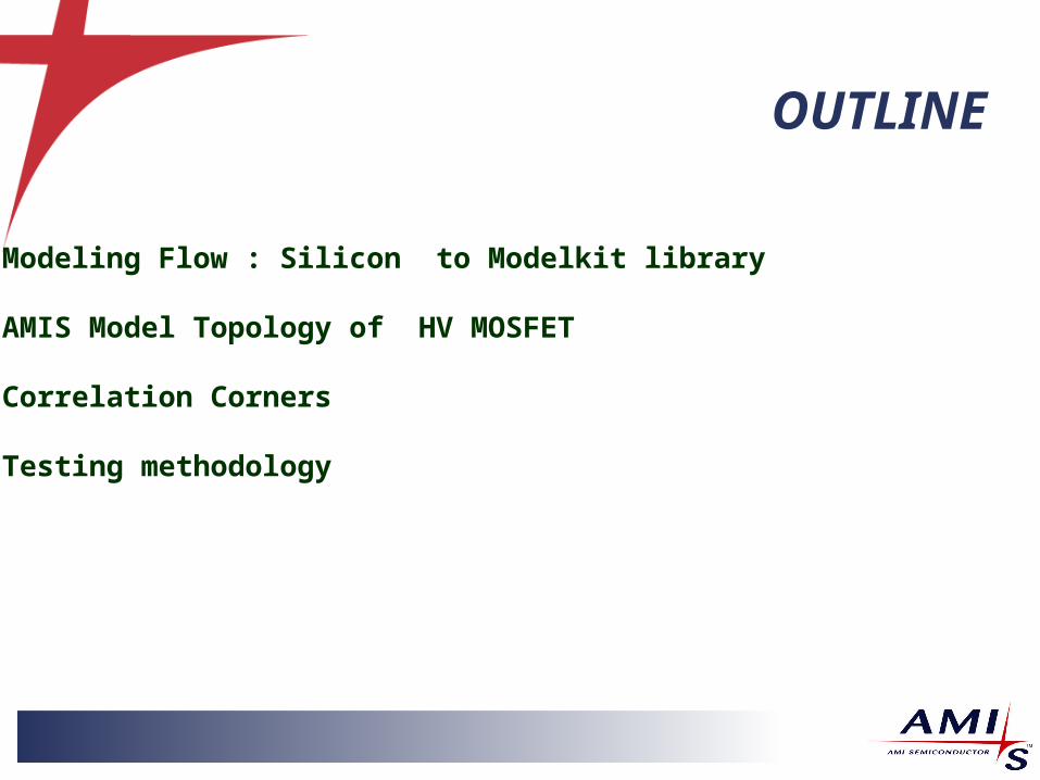
OUTLINE
1/ Modeling Flow : Silicon to Modelkit library
2/ AMIS Model Topology of HV MOSFET
3/ Correlation Corners
4/ Testing methodology
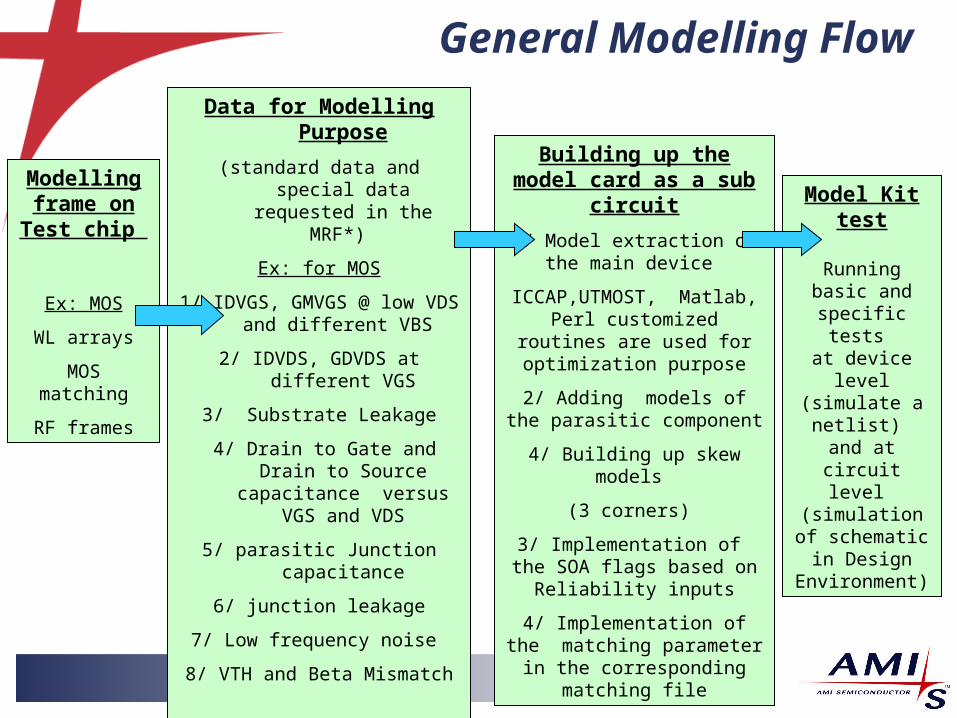
General Modelling Flow
Data for Modelling Purpose
(standard data and special data requested in the MRF*)
Ex: for MOS
1/ IDVGS, GMVGS @ low VDS and different VBS
2/ IDVDS, GDVDS at different VGS
3/ Substrate Leakage
4/ Drain to Gate and Drain to Source capacitance versus
VGS and VDS
5/ parasitic Junction capacitance
6/ junction leakage
7/ Low frequency noise
8/ VTH and Beta Mismatch
Building up the model card as a sub circuit
1/ Model extraction of the main device
ICCAP,UTMOST, Matlab, Perl customized routines are used
for optimization purpose
2/ Adding models of the parasitic component
4/ Building up skew models
(3 corners)
3/ Implementation of the SOA flags based on Reliability
inputs
4/ Implementation of the matching parameter in the
corresponding matching file
Modelling frame on Test chip
Ex: MOS
WL arrays
MOS matching
RF frames
Model Kit test
Running basic and specific
tests at device level
(simulate a netlist)
and at circuit level
(simulation of schematic in
Design Environment)
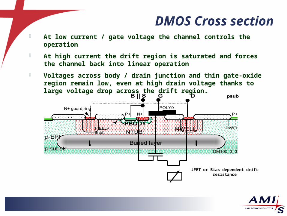
DMOS Cross section At low current / gate voltage the channel controls the operation
At high current the drift region is saturated and forces the channel back into linear operation
Voltages across body / drain junction and thin gate-oxide region remain low, even at high drain voltage thanks to large voltage drop across the drift region.
JFET or Bias dependent drift resistance
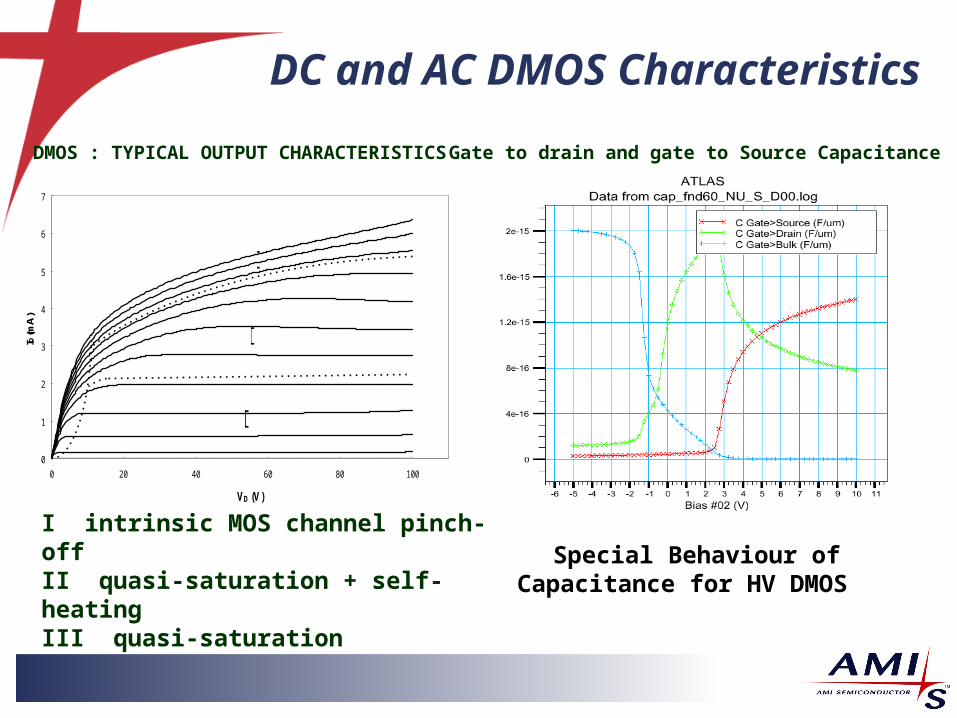
DC and AC DMOS Characteristics
0
1
2
3
4
5
6
7
0 20 40 60 80 100
VD (V)
I D(m
A)
VG=12V
10V
8V
6V
4V
2V
3V
5V
7V
9V
11V
I
II
III
DMOS : TYPICAL OUTPUT CHARACTERISTICS
I intrinsic MOS channel pinch-offII quasi-saturation + self-heatingIII quasi-saturation
Gate to drain and gate to Source Capacitance
Special Behaviour of Capacitance for HV DMOS
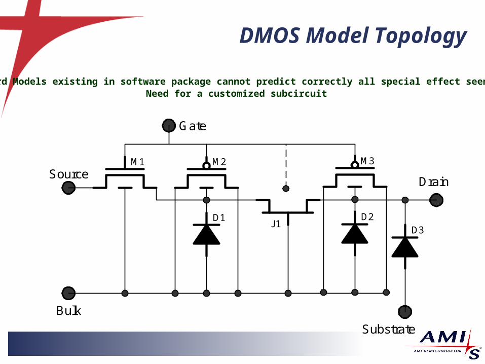
DMOS Model Topology
Standard Models existing in software package cannot predict correctly all special effect seen in DMOSNeed for a customized subcircuit
Gate
SourceDrain
Bulk
Substrate
M1 M2
D1D3
J1
M3
D2
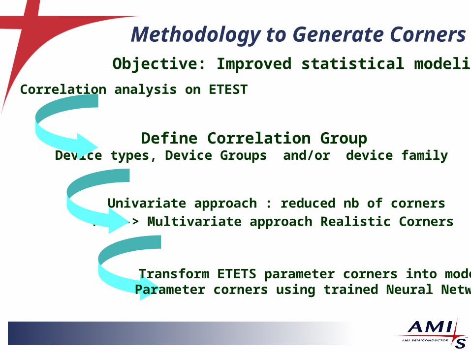
Methodology to Generate Corners
Correlation analysis on ETEST
Define Correlation GroupDevice types, Device Groups and/or device family
Objective: Improved statistical modeling
Univariate approach : reduced nb of corners
PCA -> Multivariate approach Realistic Corners
Transform ETETS parameter corners into model Parameter corners using trained Neural Network
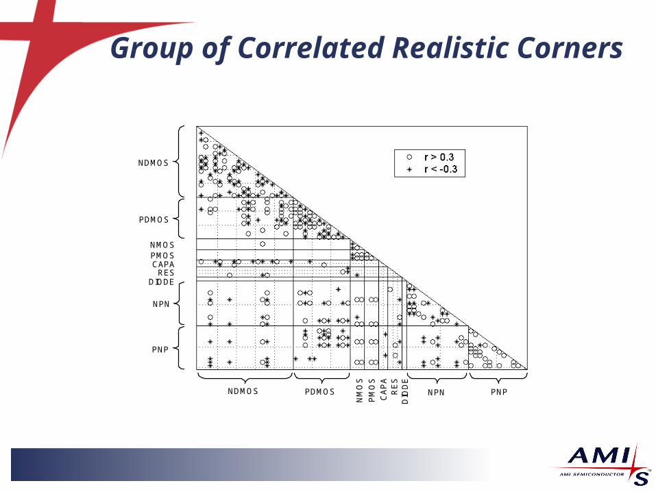
Group of Correlated Realistic Corners
NDMOS
PDMOS
NPN
PNP
NMOS PMOS CAPA
RES DIODE
NDMOS PDMOS NPN PNP
NM
OS
PM
OS
CA
PA
R
ES
D
IOD
E
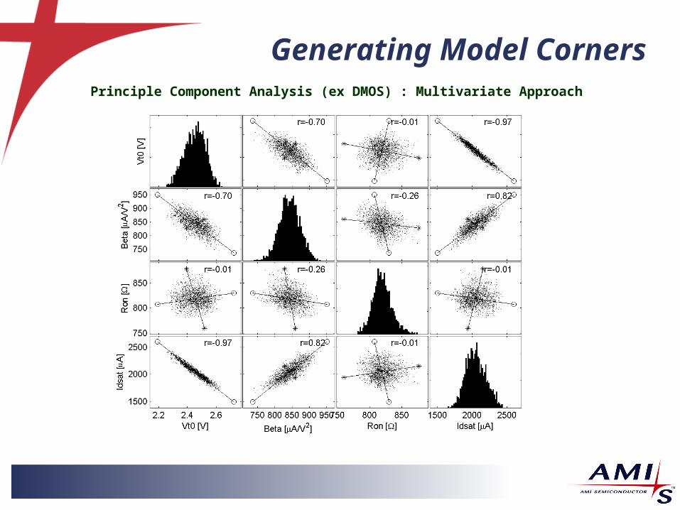
Generating Model Corners Principle Component Analysis (ex DMOS) : Multivariate Approach
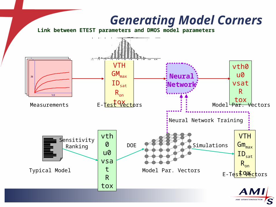
Generating Model Corners Link between ETEST parameters and DMOS model parameters
Id
Vd
Id
Vd
Id
Vd
VTHGMmax
IDsat
Ron
tox
vth0
u0vsat
Rtox
VTHGmmax
IDsat
Ron
tox
NeuralNetwork
vth0u0
vsatR
toxMeasurements
Model Par. Vectors
E-Test Vectors Model Par. Vectors
Simulations
Typical Model
DOESensitivity Ranking
E-Test Vectors
Neural Network Training
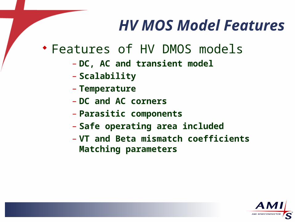
HV MOS Model Features Features of HV DMOS models
– DC, AC and transient model– Scalability– Temperature– DC and AC corners– Parasitic components – Safe operating area included– VT and Beta mismatch coefficients Matching
parameters
Testing the Model Kit
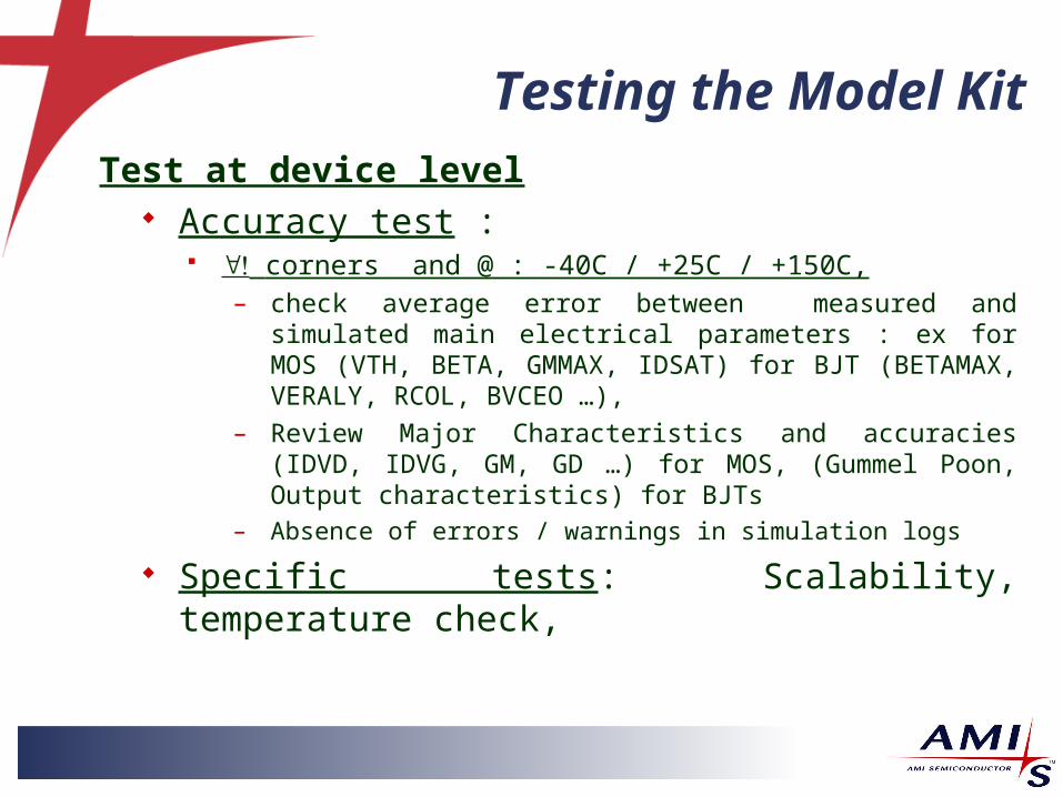
Test at device level Accuracy test :
corners and @ : -40C / +25C / +150C, – check average error between measured and simulated
main electrical parameters : ex for MOS (VTH, BETA, GMMAX, IDSAT) for BJT (BETAMAX, VERALY, RCOL, BVCEO …),
– Review Major Characteristics and accuracies (IDVD, IDVG, GM, GD …) for MOS, (Gummel Poon, Output characteristics) for BJTs
– Absence of errors / warnings in simulation logs
Specific tests: Scalability, temperature check,
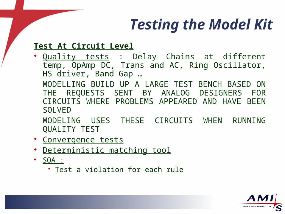
Testing the Model KitTest At Circuit Level Quality tests : Delay Chains at different temp, OpAmp DC,
Trans and AC, Ring Oscillator, HS driver, Band Gap …MODELLING BUILD UP A LARGE TEST BENCH BASED ON THE REQUESTS SENT BY ANALOG DESIGNERS FOR CIRCUITS WHERE PROBLEMS APPEARED AND HAVE BEEN SOLVED MODELING USES THESE CIRCUITS WHEN RUNNING QUALITY TEST
Convergence tests Deterministic matching tool SOA :
Test a violation for each rule
Conclusion
• Review HV Modeling Methodology in AMIS
• HV Model Perspective:
Aging Model Self Heating