Embed Size (px)
Citation preview
GeneralSpecifications
<<Contents>> <<Index>>
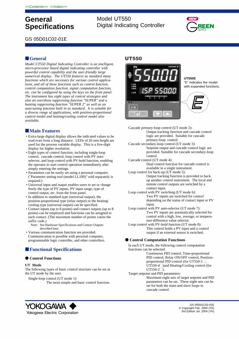
Model UT550Digital Indicating Controller
GS 05D01C02-01E
GS 05D01C02-01E© Copyright Feb. 2000 (YK)
3rd Edition Jul. 2004 (YK)
UT550 GeneralModel UT550 Digital Indicating Controller is an intelligent,micro-processor based digital indicating controller withpowerful control capability and the user-friendly largenumerical display. The UT550 features as standard manyfunctions which are necessary for various control applica-tions, and all of these functions such as control function,control computation function, signal computation function,etc. can be configured by using the keys on the front panel.The instrument has eight types of control strategies andalso an overshoot suppressing function "SUPER" and ahunting suppressing function "SUPER 2" as well as anauto-tuning function built in as standard. It is suitable fora diverse range of applications, with position-proportionalcontrol model and heating/cooling control model alsoavailable.
Main Features• Extra-large digital display allows the indicated values to be
read even from a long distance. LEDs of 20 mm height areused for the process variable display. This is a five-digitdisplay for higher resolution.
• Eight types of control function, including single-loopcontrol, cascade control, loop control with PV auto-selector, and loop control with PV-hold function, enablingthe operator to start control operation immediately aftersimply entering the settings.
• Parameters can be easily set using a personal computer.("Parameter setting tool (model LL100)" sold separately isrequired.)
• Universal input and output enables users to set or changefreely the type of PV inputs, PV input range, type ofcontrol output, etc. from the front panel.
• In addition to standard type (universal output), theposition-proportional type (relay output) or the heating/cooling type (universal output) can be specified.
• Contact inputs (up to 8 points) and contact outputs (up to 8points) can be employed and functions can be assigned toeach contact. (The maximum number of points varies thesuffix code.)
Note: See Hardware Specifications and Contact Outputsdescribed later.
• Various communication function are provided.Communication is possible with personal computer,programmable logic controller, and other controllers.
Functional Specifications
Control Functions
UT ModeThe following types of basic control structure can be set asthe UT mode by the user.
Single-loop control (UT mode 1):The most simple and basic control function.
Cascade primary-loop control (UT mode 2):Output tracking function and cascade controllogic are provided. Suitable for cascadeprimary-loop control.
Cascade secondary-loop control (UT mode 3):Setpoint output and cascade control logic areprovided. Suitable for cascade secondary-loopcontrol.
Cascade control (UT mode 4):Dual control function for cascade control isavailable in a single instrument.
Loop control for back-up (UT mode 5):Output tracking function is provided to backup another control instrument. The local andremote control outputs are switched by acontact input.
Loop control with PV switching (UT mode 6):Two PV inputs are switched for controldepending on the status of contact input or PVinput.
Loop control with PV auto-selector (UT mode 7):Two PV inputs are automatically selected forcontrol with a high, low, average, or tempera-ture-difference value selector.
Loop control with PV-hold function (UT mode 8):This control holds a PV input and a controloutput if an external sensor is switched.
Control Computation FunctionsIn each UT mode, the following control computationfunctions can be selected:
Continuous PID control, Time-proportionalPID control, Relay ON/OFF control, Position-proportional PID control (for UT550-1 ,UT550-4 )and Heating/Cooling control (forUT550-2 ).
Target setpoint and PID parameters:Maximum eight sets of target setpoint and PIDparameters can be set. These eight sets can beset for both the main and slave loops incascade control.
UT550E“E” indicates the modelwith expanded functions.
2
All Rights Reserved. Copyright © 2000, Yokogawa Electric Corporation
<<Contents>> <<Index>>
GS 05D01C02-01E 3rd Edition Jul. 30, 2004-00
Zone PID selection:Dividing PV input range into maximum 7zones by maximum 6 reference points, PIDparameter set switching in up to 7 PV inputzones.
Auto-tuning:Available as standard. Possible to activateauto-tuning for both main and slave loops forcascade control.
"SUPER" function:Overshoots generated by abrupt changes in thetarget setpoint or by disturbances can besuppressed.
"SUPER 2" function:This function stabilizes the state of controlthat is unstable due to hunting, etc. withoutrequiring any change in PID constants, whenthe load and/or gain varies greatly, or whenthere is a difference between the characteris-tics of temperature zones.
Preset output function:When the instrument is in STOP mode, PVinput is burnt-out, or an abnormality is foundin an input circuit, a preset value is output as acontrol output.
Sampling periodEach sampling period can be selected underthe following conditions:
50 ms: Available for model code UT550-00, whenUT mode is set to Single-loop control andthe following functions are not used:"SUPER" function, "SUPER 2" function,heating/cooling control, PV input computa-tion, setpoint rate-of-change limiter, MVoutput rate-of-change limiter, deviationalarm, sensor grounding alarm, faultdiagnosis alarm, and FAIL output.
100 ms: Available when UT mode is not cascadecontrol.
200 ms: Available when UT mode is cascade control.(Set value when shipped from the factory: 200 ms)500 ms: Always available.
Operation Mode Switching(Note: Communication enables all the following
mode switching to be executed.)AUTO/MANUAL switching:
Bumpless switching between automaticoperation mode and manual control mode isavailable by using the front keys or contactinput. The contact input has priority overfront key input or switching by communica-tion. The contact input is invalid for Cascadesecondary-loop control or Cascade control.
RUN/STOP switching:Switching by contact input (bumpless forswitching from STOP to RUN). The contactinput has priority over switching by communi-cation. In RUN mode, control computation isactivated. In STOP mode, control computa-tion ceases and a preset value is output as acontrol output while other functions operatenormally.
REMOTE/LOCAL switching:Switching between remote setpoint and localsetpoint by instrument operation or contactinput. The contact input has priority overinstrument operation or switching bycommunication. For remote to local switch-ing, either bumpless tracking (employing theremote setpoint on switching as the localsetpoint) or without tracking (directlyswitching the local setpoint) can be specified.
CASCADE/AUTO/MANUAL switching:Switching by instrument operation or contactinput. The contact input has priority overinstrument operation or switching bycommunication. Valid for Cascade second-ary-loop control or Cascade control.
Output tracking ON/OFF switching:Provided for Cascade primary-loop control orLoop control for backup. External trackingsignal and internal control output are switchedby the contact input. The contact input haspriority over the switching by communication.
Control Parameters Setting RangeProportional band: 0.1 to 999.9%
0.0 to 999.9% (for heating/cooling PIDcontrol), 0.0% available for ON/OFF control
Integral time: 1 to 6,000 s, or OFF (for Manual reset)Derivative time: 1 to 6,000 s, or OFFON/OFF control hysteresis: 0.0 to 100.0% of PV input
range spanPreset output: -5.0 to 105.0% (0 mA or less cannot be
output)Output limiter:
Setting range: -5.0 to 105.0% for both highand low limitsHowever, "low limit setpoint < high limitsetpoint" must be satisfied.In case of heating/cooling PID control, upperlimiter for heating and upper limiter forcooling.
Shutdown function:When manual control is carried out with 4 to20 mA output, control output can be outputdown to about 0 mA (shutdown is specifiedfor -5.0% or less).
Rate-of-change limiter for output:OFF or 0.1 to 100.0%/s
Deadband for heating/cooling control:-100.0 to 50.0% for output value
Deadband for position-proportional control:1.0 to 10.0% for output
Configuration of Input/Output Signal
PV Input ComputationsInput processing, Square root extraction (voltage input only,Input low cut 0.0 to 5.0%), Ten-segment linearizer function,Ten-segment bias, Bias addition (-100.0 to 100.0%), andFirst order lag filter (OFF, time constant 1 to 120 s)
Auxiliary Input Computations(Applied to remote setting input only)
Input processing, Square root extraction (Input low cut 0.0 to5.0%), Bias addition (-100.0 to 100.0%), Ratio multiplication(0.001 to 9.999), First order lag filter (OFF, time constant 1to 120 s)
3<<Contents>> <<Index>>
All Rights Reserved. Copyright © 2000, Yokogawa Electric Corporation GS 05D01C02-01E 3rd Edition Jul. 30, 2004-00
Alarm FunctionsAlarm types:
PV high limit, PV low limit, Deviation highlimit, Deviation low limit, Deenergized ondeviation high limit, Deenergized on deviationlow limit, Deviation high and low limits, Highand low limits within deviation, Deenergizedon PV high limit, Deenergized on PV lowlimit, SP high limit, SP low limit, Output highlimit, Output low limit.
Alarm setting range:PV/SP alarm: -100 to 100% of PV input rangeDeviation alarm: -100 to 100% of PV inputrange spanOutput alarm: -5.0 to 105.0% of output valueAlarm hysteresis: 0.0 to 100.0% of PV inputrange span
Delay timer:0.00 to 99.59 (minute, second)An alarm is output when the delay timerexpires after the alarm setpoint is reached.Setting for each alarm is possible.
Stand-by action:Stand-by action can be set to make PV/deviation alarm OFF during start-up or afterSP change until SP reaches the normal region.
Timer function (stabilization of control status notificationevent) (Alarm 1 only):This function sets the alarm 1 output to ONwhen a preset time (timer setting) elapses aftera PV has reached the control target setpointhysteresis band to notify that control hasreached its stabilized status. Restarted inRUN/STOP or SP switching.
Other alarm actions:Sensor grounding alarm: Detects sensordeterioration and outputs an alarm.Fault-diagnosis alarm: For input burnout, A/Dconversion error, or thermocouple referencejunction compensation error.FAIL output: Abnormality in software orhardware.
Number of alarm settings: 8 (maximum)The alarm status can be read via communica-tion in addition to output as the above alarmoutput.
Alarm output points (see also the item "Contact Outputs")• Number of contact (relay) outputs:
3 (standard) or 4 (if a control output relay isused for the alarm 4 output relay.)
• Number of contact (transistor open collector)outputs:4 (when optional function code is specifiedas 1 or 3)
From the above, up to 8 point outputs can be obtained(except for cascade control).Any of PV alarm, deviation alarm, SP alarm, output alarm,Fault-diagnosis alarm, sensor grounding alarm and FAILoutput can be assigned to contacts for the above number ofoutputs. However, the timer delay alarm can be assignedto the alarm 1 output only. Also, the alarm 4 only can beassigned to the control output relay (if a relay is not usedfor control output).
Display and Operation Functions
PV Disp layPV is displayed in the 5-digit display. PV1 or PV2 isdisplayed by switching them in cascade control. The numberof display digits is 4 or 5. For thermocouple or RTD, databelow the decimal point can be set not to display. Thedisplay range is -19999 to 30000 and the display span is30000 or less. [550.00 appearing in the product photographon page 1 cannot actually be displayed.]
Setpoint Disp layA parameter name is displayed in the 3-digit display and datain the 5-digit display. There are four kinds of displays :operating display, operating parameter setting display, setupparameter setting display and SELECT display.
Operating display:Data necessary for operations, such as setpointor control output, are displayed depending onthe UT mode.
Operating parameters setting display:The Operating parameters, which are mainlychanged during operations, such as PIDconstant, are displayed.
Setup parameters setting display:The Setup parameters to configure thefunctions of the instrument before startingoperation are displayed.UT mode is to be set in this display.
SELECT display:Up to five displays which are frequentlyaccessed can be selected from the Operatingparameters setting display and Setup param-eters setting display to be displayed in theSELECT display.
Status Indicator LampsAlarm indicator lamps:
Four lamps, AL1, AL2, AL3, and AL4Status indicator lamps:
REM (remote operation), MAN (manual modeoperation), CAS (cascade operation), and LP2(cascade secondary-loop control)
Deviation monitor:Plus deviation, Minus deviation, and deviation in normal range
Operat ion Keys, keys: Increase or decrease setpoints and other
parameters displayed in the setpoint display.SET/ENT key: Used for setting or changing set data,
switching the displayed contents, andswitching operation modes except for A/M.
A/M key: Operation mode switching (Auto/Manual)
Security FunctionKey-lock by parameter setting and prohibitingoperation by a password are available.
4
All Rights Reserved. Copyright © 2000, Yokogawa Electric Corporation
<<Contents>> <<Index>>
GS 05D01C02-01E 3rd Edition Jul. 30, 2004-00
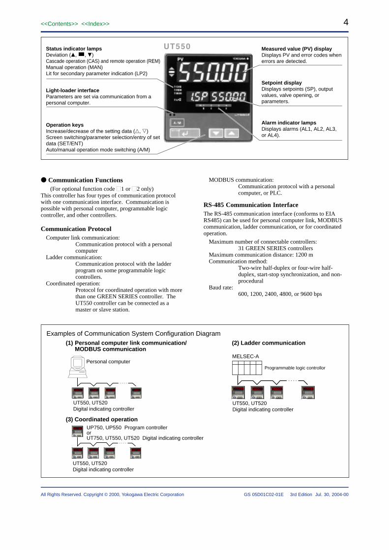
Status indicator lampsDeviation (, , )Cascade operation (CAS) and remote operation (REM)Manual operation (MAN)Lit for secondary parameter indication (LP2)
Light-loader interfaceParameters are set via communication from a personal computer.
Measured value (PV) display Displays PV and error codes when errors are detected.
Setpoint display Displays setpoints (SP), output values, valve opening, or parameters.
Alarm indicator lampsDisplays alarms (AL1, AL2, AL3, or AL4).
Operation keysIncrease/decrease of the setting data (, )Screen switching/parameter selection/entry of set data (SET/ENT)Auto/manual operation mode switching (A/M)
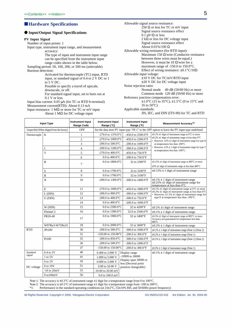
Communication Functions(For optional function code 1 or 2 only)
This controller has four types of communication protocolwith one communication interface. Communication ispossible with personal computer, programmable logiccontroller, and other controllers.
Communication ProtocolComputer link communication:
Communication protocol with a personalcomputer
Ladder communication:Communication protocol with the ladderprogram on some programmable logiccontrollers.
Coordinated operation:Protocol for coordinated operation with morethan one GREEN SERIES controller. TheUT550 controller can be connected as amaster or slave station.
MODBUS communication:Communication protocol with a personalcomputer, or PLC.
RS-485 Communication InterfaceThe RS-485 communication interface (conforms to EIARS485) can be used for personal computer link, MODBUScommunication, ladder communication, or for coordinatedoperation.
Maximum number of connectable controllers:31 GREEN SERIES controllers
Maximum communication distance: 1200 mCommunication method:
Two-wire half-duplex or four-wire half-duplex, start-stop synchronization, and non-procedural
Baud rate:600, 1200, 2400, 4800, or 9600 bps
A/M
STPCAS
MAN1REM
MAN2
PVPV2
AL
DISPSET/ENT
A/M
STPCAS
MAN1REM
MAN2
PVPV2
AL
DISPSET/ENT
A/M
STPCAS
MAN1REM
MAN2
PVPV2
AL
DISPSET/ENT
A/M
STPCAS
MAN1REM
MAN2
PVPV2
AL
DISPSET/ENT
A/M
STPCAS
MAN1REM
MAN2
PVPV2
AL
DISPSET/ENT
A/M
STPCAS
MAN1REM
MAN2
PVPV2
AL
DISPSET/ENT
A/M
STPCAS
MAN1REM
MAN2
PVPV2
AL
DISPSET/ENT
A/M
STPCAS
MAN1REM
MAN2
PVPV2
AL
DISPSET/ENT
A/M
STPCAS
MAN1REM
MAN2
PVPV2
AL
DISPSET/ENT
A/M
STPCAS
MAN1REM
MAN2
PVPV2
AL
DISPSET/ENT
A/M
STPCAS
MAN1REM
MAN2
PVPV2
AL
DISPSET/ENT
A/M
STPCAS
MAN1REM
MAN2
PVPV2
AL
DISPSET/ENT
A/M
1
STPCAS
MAN1REM
MAN2
PVPV2
AL
DISPSET/ENT
Personal computerMELSEC-A
UT550, UT520Digital indicating controller
UP750, UP550 Program controllerorUT750, UT550, UT520 Digital indicating controller
UT550, UT520Digital indicating controller
UT550, UT520Digital indicating controller
(1) Personal computer link communication/ MODBUS communication
(2) Ladder communication
(3) Coordinated operation
Programmable logic controllor
Examples of Communication System Configuration Diagram
5<<Contents>> <<Index>>
All Rights Reserved. Copyright © 2000, Yokogawa Electric Corporation GS 05D01C02-01E 3rd Edition Jul. 30, 2004-00
Hardware Specifications
Input/Output Signal Specifications
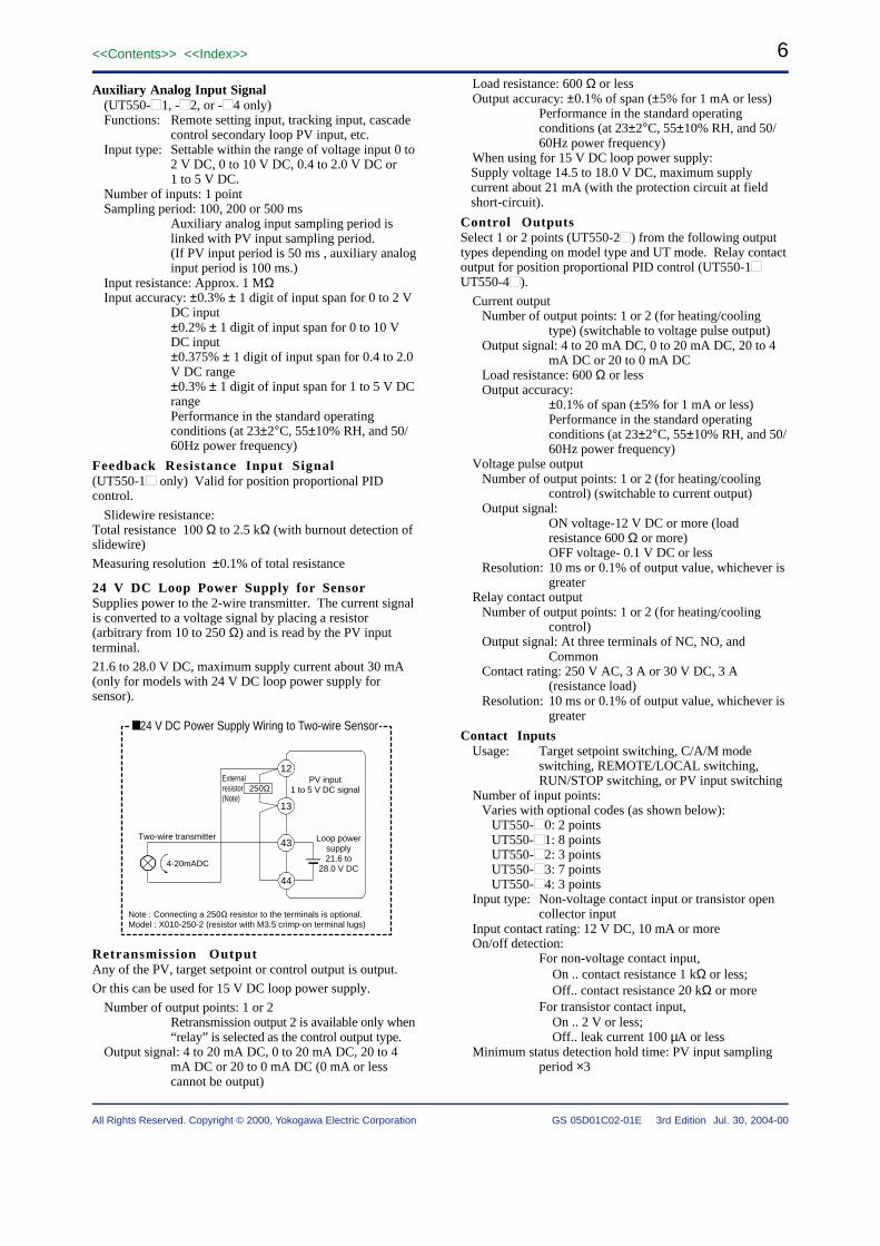
PV Input SignalNumber of input points: 1Input type, instrument input range, and measurement
accuracy:The type of input and instrument input rangecan be specified from the instrument inputrange codes shown in the table below.
Sampling period: 50, 100, 200, or 500 ms (selectable)Burnout detection:
Activated for thermocouple (TC) input, RTDinput, or standard signal of 0.4 to 2 V DC or 1to 5 V DC.Possible to specify a travel of upscale,downscale, or off.For standard signal input, set to burn out at0.1 V or less.
Input bias current: 0.05 µA (for TC or RTD b-terminal)Measurement current(RTD): About 0.13 mAInput resistance: 1 MΩ or more for TC or mV input
About 1 MΩ for DC voltage input
Allowable signal source resistance:250 Ω or less for TC or mV inputSignal source resistance effect
0.1 µV/Ω or less2 kΩ or less for DC voltage inputSignal source resistance effect
About 0.01%/100 ΩAllowable wiring resistance (for RTD input):
Maximum 150 Ω/wire (Conductor resistancebetween three wires must be equal.)However, it must be 10 Ω/wire for amaximum range of -150.0 to 150.0°C.Effect of wiring resistance: ±0.1°C/10Ω
Allowable input voltage:±10 V DC for TC/mV/RTD input±20 V DC for DC voltage input
Noise rejection ratio:Normal mode 40 dB (50/60 Hz) or moreCommon mode 120 dB (50/60 Hz) or more
Reference junction compensation error:±1.0°C (15 to 35°C), ±1.5°C (0 to 15°C and35 to 50°C)
Applicable standards:JIS, IEC, and DIN (ITS-90) for TC and RTD
Unspecified (When shipped from the factory) OFF Set the data item PV input type “IN 1” to the OFF option to leave the PV input type undefined.
Instrument InputRange (°C)
Instrument InputRange (°F)
-270.0 to 1370.0°C
-270.0 to 1000.0°C
-200.0 to 500.0°C
-200.0 to 1200.0°C
-270.0 to 400.0°C
0.0 to 400.0°C
0.0 to 1800.0°C
0.0 to 1700.0°C
0.0 to 1700.0°C
-200.0 to 1300.0°C
-270.0 to 1000.0°C
-200.0 to 900.0°C
-200.0 to 400.0°C
0.0 to 400.0°C
0.0 to 2300.0°C
0.0 to 1390.0°C
0.0 to 1900.0°C
0.0 to 2000.0°C
-200.0 to 500.0°C
-150.00 to 150.00°C
-200.0 to 850.0°C
-200.0 to 500.0°C
-150.00 to 150.00°C
Thermocouple
RTD
Standard signal
DC voltage
K
J
T
B
S
R
N
E
L (DIN)
U (DIN)
W (DIN)
Platinel 2
PR20-40
W97Re3-W75Re25
JPt100
Pt100
0.4 to 2V
1 to 5V
0 to 2V
0 to 10V
-10 to 20mV
0 to100mV
1
2
3
4
5
6
7
8
9
10
11
12
13
14
15
16
17
18
30
31
35
36
37
40
41
50
51
55
56
±0.1% ±1 digit of instrument range at 0°C or more±0.2% ±1 digit of instrument range at less than 0°C• However, ±2% ±1 digit of instrument range for type K
at temperatures less than -200°C.• However, ±1% ± 1 digit of instrument range for type T
at temperatures less than -200°C.
±0.15% ±1 digit of instrument range at 400°C or more
±5% ±1 digit of instrument range at less than 400°C
±0.15% ± 1 digit of instrument range
±0.1% ± 1 digit of instrument range±0.25% ±1 digit of instrument range for temperature at less than 0°C±0.1% ±1 digit of instrument range at 0°C or more±0.2% ±1 digit of instrument range at less than 0°C• However, ±1.5% ±1 digit of instrument range for
type E at temperature less than -200°C.
±0.2% ±1 digit of instrument range
±0.1% ± 1 digit of instrument range±0.5% ±1 digit of instrument range at 800°C or moreAccuracy not guaranteed for temperature less than 800°C
±0.2% ± 1 digit of instrument range
±0.1% ± 1 digit of instrument range (Note 1) (Note 2)
±0.2% ± 1 digit of instrument range (Note 1)
±0.1% ± 1 digit of instrument range (Note 1) (Note 2)
±0.2% ± 1 digit of instrument range (Note 1)
±0.1% ± 1 digit of instrument range
Input Type Measurement Accuracy*1Instrument Input Range Code
Display range-19999 to 30000Display span 30000 or less (Decimal point position changeable)
0.400 to 2.000 V
1.000 to 5.000 V
0.000 to 2.000 V
0.00 to 10.00 V
-10.00 to 20.00 mV
0.0 to 100.0 mV
-450.0 to 2500.0°F
-450.0 to 2300.0°F
-200.0 to 1000.0°F
-300.0 to 2300.0°F
-450.0 to 750.0°F
-200.0 to 750.0°F
32 to 3300°F
32 to 3100°F
32 to 3100°F
-300.0 to 2400.0°F
-450.0 to 1800.0°F
-300.0 to 1600.0°F
-300.0 to 750.0°F
-200.0 to 1000.0°F
32 to 4200°F
32.0 to 2500.0°F
32 to 3400°F
32 to 3600°F
-300.0 to 1000.0°F
-200.0 to 300.0°F
-300.0 to 1560.0°F
-300.0 to 1000.0°F
-200.0 to 300.0°F
Note 1: The accuracy is ±0.3°C of instrument range ±1 digit for a temperature range from 0 to 100°C.Note 2: The accuracy is ±0.5°C of instrument range ±1 digit for a temperature range from -100 to 200°C.*1: Performance in the standard operating conditions (at 23±2°C, 55±10% RH, and 50/60Hz power frequency)
6
All Rights Reserved. Copyright © 2000, Yokogawa Electric Corporation
<<Contents>> <<Index>>
GS 05D01C02-01E 3rd Edition Jul. 30, 2004-00
Auxiliary Analog Input Signal(UT550- 1, - 2, or - 4 only)Functions: Remote setting input, tracking input, cascade
control secondary loop PV input, etc.Input type: Settable within the range of voltage input 0 to
2 V DC, 0 to 10 V DC, 0.4 to 2.0 V DC or1 to 5 V DC.
Number of inputs: 1 pointSampling period: 100, 200 or 500 ms
Auxiliary analog input sampling period islinked with PV input sampling period.(If PV input period is 50 ms , auxiliary analoginput period is 100 ms.)
Input resistance: Approx. 1 MΩInput accuracy: ±0.3% ± 1 digit of input span for 0 to 2 V
DC input±0.2% ± 1 digit of input span for 0 to 10 VDC input±0.375% ± 1 digit of input span for 0.4 to 2.0V DC range±0.3% ± 1 digit of input span for 1 to 5 V DCrangePerformance in the standard operatingconditions (at 23±2°C, 55±10% RH, and 50/60Hz power frequency)
Feedback Resistance Input Signal(UT550-1 only) Valid for position proportional PIDcontrol.
Slidewire resistance:Total resistance 100 Ω to 2.5 kΩ (with burnout detection ofslidewire)
Measuring resolution ±0.1% of total resistance
24 V DC Loop Power Supply for SensorSupplies power to the 2-wire transmitter. The current signalis converted to a voltage signal by placing a resistor(arbitrary from 10 to 250 Ω) and is read by the PV inputterminal.
21.6 to 28.0 V DC, maximum supply current about 30 mA(only for models with 24 V DC loop power supply forsensor).
12
13
43
44
Two-wire transmitter
4-20mADC
250Ω
24 V DC Power Supply Wiring to Two-wire Sensor
Externalresistor(Note)
PV input1 to 5 V DC signal
Loop powersupply21.6 to
28.0 V DC
Note : Connecting a 250Ω resistor to the terminals is optional.Model : X010-250-2 (resistor with M3.5 crimp-on terminal lugs)
Retransmission OutputAny of the PV, target setpoint or control output is output.
Or this can be used for 15 V DC loop power supply.
Number of output points: 1 or 2Retransmission output 2 is available only when“relay” is selected as the control output type.
Output signal: 4 to 20 mA DC, 0 to 20 mA DC, 20 to 4mA DC or 20 to 0 mA DC (0 mA or lesscannot be output)
Load resistance: 600 Ω or lessOutput accuracy: ±0.1% of span (±5% for 1 mA or less)
Performance in the standard operatingconditions (at 23±2°C, 55±10% RH, and 50/60Hz power frequency)
When using for 15 V DC loop power supply:Supply voltage 14.5 to 18.0 V DC, maximum supplycurrent about 21 mA (with the protection circuit at fieldshort-circuit).
Control OutputsSelect 1 or 2 points (UT550-2 ) from the following outputtypes depending on model type and UT mode. Relay contactoutput for position proportional PID control (UT550-1UT550-4 ).
Current outputNumber of output points: 1 or 2 (for heating/cooling
type) (switchable to voltage pulse output)Output signal: 4 to 20 mA DC, 0 to 20 mA DC, 20 to 4
mA DC or 20 to 0 mA DCLoad resistance: 600 Ω or lessOutput accuracy:
±0.1% of span (±5% for 1 mA or less)Performance in the standard operatingconditions (at 23±2°C, 55±10% RH, and 50/60Hz power frequency)
Voltage pulse outputNumber of output points: 1 or 2 (for heating/cooling
control) (switchable to current output)Output signal:
ON voltage-12 V DC or more (loadresistance 600 Ω or more)OFF voltage- 0.1 V DC or less
Resolution: 10 ms or 0.1% of output value, whichever isgreater
Relay contact outputNumber of output points: 1 or 2 (for heating/cooling
control)Output signal: At three terminals of NC, NO, and
CommonContact rating: 250 V AC, 3 A or 30 V DC, 3 A
(resistance load)Resolution: 10 ms or 0.1% of output value, whichever is
greater
Contact InputsUsage: Target setpoint switching, C/A/M mode
switching, REMOTE/LOCAL switching,RUN/STOP switching, or PV input switching
Number of input points:Varies with optional codes (as shown below):
UT550- 0: 2 pointsUT550- 1: 8 pointsUT550- 2: 3 pointsUT550- 3: 7 pointsUT550- 4: 3 points
Input type: Non-voltage contact input or transistor opencollector input
Input contact rating: 12 V DC, 10 mA or moreOn/off detection:
For non-voltage contact input, On .. contact resistance 1 kΩ or less; Off.. contact resistance 20 kΩ or moreFor transistor contact input, On .. 2 V or less; Off.. leak current 100 µA or less
Minimum status detection hold time: PV input samplingperiod ×3
7<<Contents>> <<Index>>
All Rights Reserved. Copyright © 2000, Yokogawa Electric Corporation GS 05D01C02-01E 3rd Edition Jul. 30, 2004-00
Contact OutputsUsage: Alarm output, FAIL outputNumber of output points:
Varies with optional codes (as shown below):UT550- 0: Relay output 3 pointsUT550- 1: Relay output 3 points, transistor output 4
pointsUT550- 2: Relay output 3 pointsUT550- 3: Relay output 3 points, transistor output 4
pointsUT550- 4: Relay output 3 points
However, when a relay is not used forcontrol output, the relay for control outputcan be used for the alarm 4. For this reason,the number of relay output points can bechanged to 4 by adding to the above 3.
Relay contact rating: 240 V AC, 1 A or 30 V DC, 1 ATransistor contact rating: 24 V DC, 50 mA
Display SpecificationsMeasured value (PV) display:
5-digit 7-segment red color LED display;height of letters 20 mm
Data display: 3 digits + 5 digits, 7-segment red colorLED display; height of letters 9.3 mm
Status indicator lamps: LEDs
Conformance to Safety and EMC StandardsSafety:Compliant with IEC/EN61010-1: 2001, approved
by CSA1010, approved by UL508.Installation category : CAT. II (IEC/EN61010,CSA1010) Pollution degree : 2 (IEC/EN61010, CSA1010)Measurement category : I (CAT. I : IEC/EN61010)Rated measurement input voltage : 10V DCmax.(across terminals), 300V AC max.(acrossground)Rated transient overvoltage : 1500V (Note)Note : It is a value on the safety standardwhich is assumed by IEC/EN61010-1 inmeasurement category I, and is not the valuewhich guarantees an apparatus performance.
EMC standards:Complies with EN61326During test, the controller continues to operatewith the measurement accuracy within ±20%of the range.
Construction, Installation, and WiringConstruction: Dust-proof and Drip-proof front panel
conforming to IP55.For side-by-side close installation, thecontroller loses its dust-proof and drip-proofprotection.
Material of the body: ABS resin and polycarbonateCase color: BlackWeight: About1 kg or lessExternal dimensions: 96W × 96H × 100D (from the panel
face) (mm)Mounting: Direct panel mounting; mounting bracket, one
each for upper and lower mounting
Panel cutout dimensions: 92+0.80 W × 92+0.8
0 H (mm)Mounting attitude:
Up to 30 degrees from horizontal; Must notface downward.
Wiring connection:With M3.5 screw terminals (for signal, powerand grounding wiring)
Power Supply and IsolationPower supply: Rated voltage 100 to 240 V AC (±10%),
50/60 HzPower consumption: Max. 20 VA (Max. 8.0 W)Data backup: Non-volatile memory. Service life about
100,000 times of writingsWithstanding voltage:
1500 V AC for 1 min.between primary terminals and secondaryterminals
1500 V AC for 1 min.between primary terminals and groundterminal
1500 V AC for 1 min.between ground terminal and secondaryterminals
500 V AC for 1 min.between secondary terminals
where primary terminals stand for powerand relay output terminals and secondaryterminals stand for analog input and output signal terminals, voltage pulse output terminals, and contact input terminals.
Isolation resistance:20 MΩ or more for 500 V DC appliedbetween power terminals and ground terminal
Grounding: Class D grounding (grounding resistance of100 Ω or less)
Isolation SpecificationsPV input terminal:
Isolated from other input/output terminals, butnot isolated from internal circuit.
Auxiliary analog input terminal:Isolated from other input/output terminals andinternal circuit.
15 V DC loop power supply terminal:Not isolated from analog current output andvoltage pulse control output, but isolated fromother input/output terminals and internalcircuit.
24 V DC loop power supply terminal:Isolated from 4-20mA analog ouptut, otherinput/output terminals and internal circuit.
Control output (current output or voltage pulse output) andretransmission output: Not isolated betweencontrol output and retransmission output, butisolated from other input/output terminals andinternal circuit.
Relay contact control output terminals:Isolated between contact output terminals, andfrom other input/output terminals and internalcircuit.
Contact input terminals:Not isolated between contact input terminalsand from communication terminals, butisolated from other input/output terminals andinternal circuit.
Relay contact output terminals:Not isolated between relay contact outputs,but isolated from other input/output terminalsand internal circuit.
8
All Rights Reserved. Copyright © 2000, Yokogawa Electric Corporation
<<Contents>> <<Index>>
GS 05D01C02-01E 3rd Edition Jul. 30, 2004-00
Transistor contact output terminals:Not isolated between transister contactoutputs, but isolated from other input/outputterminals and internal circuit.
RS-485 communication terminals:Not isolated from contact input terminals, butisolated from other input/output terminals andinternal circuit.
Feedback slidewire resistance input terminals:Not isolated from control output terminals(current or voltage pulse output) andretransmmision output, but isolated from otherinput/output terminals and internal circuit.
Power terminals:Isolated from other input/output terminals andinternal circuit.
Ground terminal:Isolated from other input/output terminals andinternal circuit.
Environmental ConditionsNormal operating conditions:
Ambient temperature: 0 to 50°C (40°C or less for side-by-side close mounting )
Temperature change rate limit: 10°C/h or lessAmbient humidity: 20 to 90% RH (no condensation)Magnetic field: 400 A/m or lessContinuous vibration (5 to 14 Hz):
Peak-to-peak amplitude 1.2 mm or lessContinuous vibration (14 to 150 Hz):
4.9 m/s2 or lessShort-period vibration: 14.7 m/s2, 15 s or lessShock: 147 m/s2 or less, 11 msInstallation altitude: 2000 m or less above sea levelWarm-up time: 30minutes or more after power on
Transportation and storage conditions:Temperature: -25 to 70°CTemperature change rate: 20°C/h or lessHumidity: 5 to 95% RH (no condensation)
Effects of operating conditionsEffect of ambient temperature:
Whichever is greater, ±1 µV/°C or ±0.01%of F.S./°C for voltage or thermocoupleinputs.±0.02% of F.S./°C for Auxiliary input±0.05°C/°C (ambient temperature) or lessfor RTD inputs.±0.05% of F.S./°C or less for analogoutputs.
Effect of power supply fluctuation (within rated voltagerange):Whichever is greater, ±1 µV/10 V or±0.01% of F.S./10 V for analog inputs.±0.05% of F.S./10 V or less for analogoutputs.
9<<Contents>> <<Index>>
All Rights Reserved. Copyright © 2000, Yokogawa Electric Corporation GS 05D01C02-01E 3rd Edition Jul. 30, 2004-00
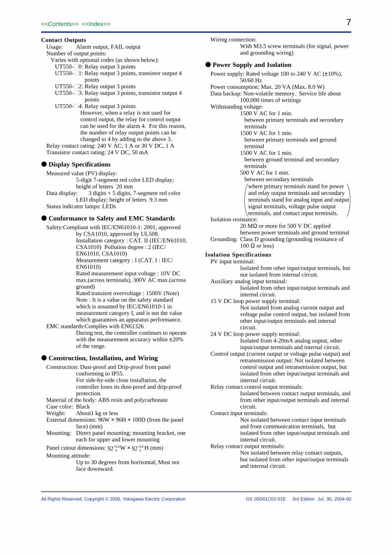
Function Block Diagram for Single-loop Control(Model UT550-0 ,UT550-2 or UT550-3 )
RMS=COMRMS=RSP
SPN
REMOTE(ON)/LOCAL(OFF) switching
CommunicationAux. Input
LOCALREMOTE
R/L
RS485
Alarm function
* Unavailable when control output is current or pulse.
AUTO(ON)/MAN(OFF) switching
STOP(ON)/RUN(OFF) switching
OT1
S/R
AUTOMAN
RUNSTOP
A/M
Control output
Current or pulse terminals
and
Relay terminals , and
Current terminals
and
OUTPUT1 OUTPUT1 OUTPUT1 OUTPUT3
15V loop power supply24V loop power supply Retransmission output
RT2 RT1
PV input terminals , and
Remote input terminals and
Communication terminals to 12 1311
1716
Terminals and 4443
LPS
Current*terminals and 1716
2 311514
DO7DO4DO3DO2DO1
DI3 DI4 DI5 DI6 DI1 DI2 DI8INPUT1 INPUT3
2221 2723
Terminal Parameter Function
Analog Signal Contact Signal Front Panel Key
Legend
Contact input
Input selection
10-seg. linearizer approx./bias
Analog input filter
PV input filter
PV input bias
Square root extraction
Unit selection
Analog input bias
Analog input range conversion
Input selection
Analog input filter
Remote setting filter
Ratio/bias calculation
Target setpoint ramp-rate function
Control computation
Preset output Output limiter
Manual operation
Target setpoints 1 to 8
Square root extraction
Unit selection
Analog input bias
Analog input range conversion
Target setpoint selection
Alarm 1 Alarm 2 Alarm 3 Alarm 4 FAIL output
ON innormalcondition
10
All Rights Reserved. Copyright © 2000, Yokogawa Electric Corporation
<<Contents>> <<Index>>
GS 05D01C02-01E 3rd Edition Jul. 30, 2004-00
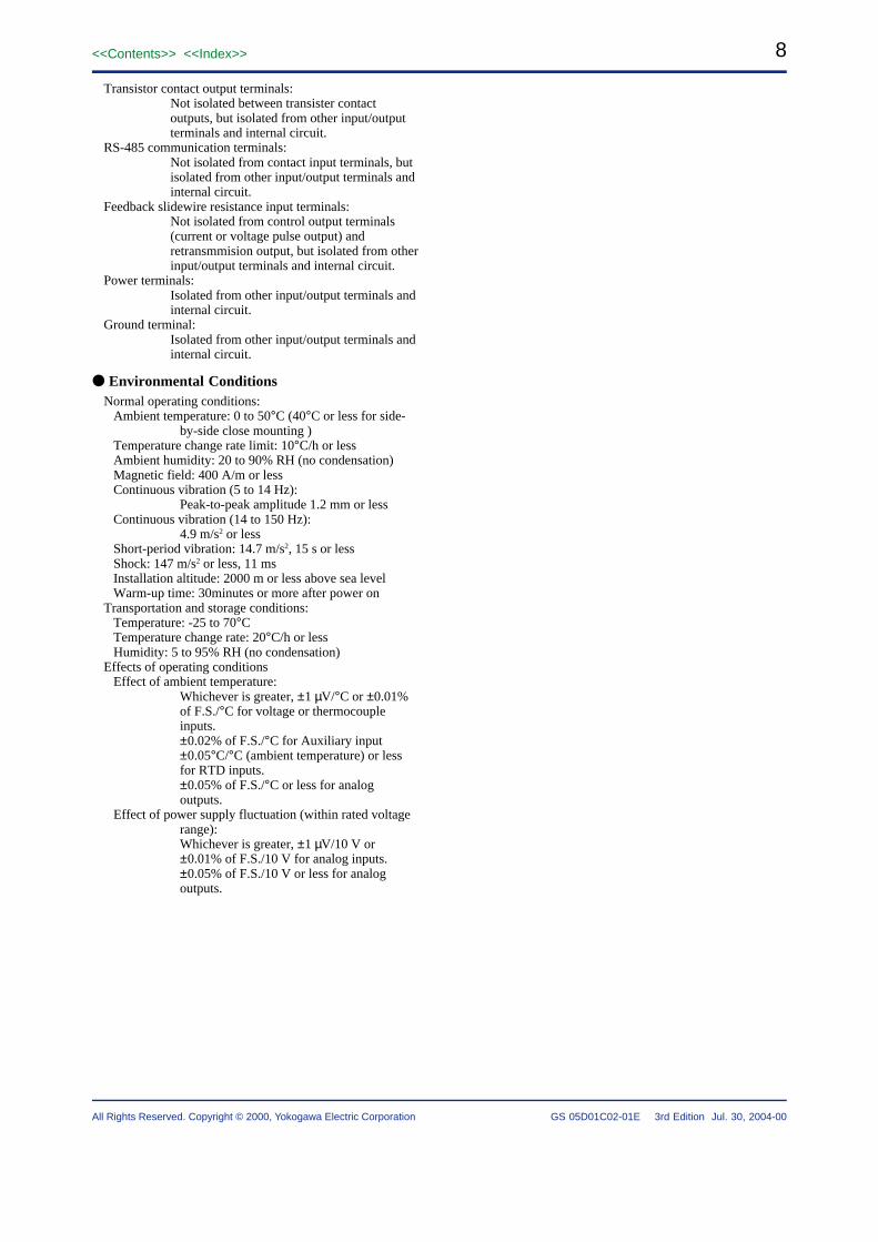
Function Block Diagram for Single-loop Heating/Cooling Control (Model UT550-2 )
RMS=COMRMS=RSP
SPN
R/L
Alarm functionOT1
A/M
Heating-side output
OUTPUT1 OUTPUT1
OT1
Cooling-side output
* Unavailable when heating-side output is current output or pulse.
OUTPUT2 OUTPUT2
Heating/cooling computation
S/R
1716 49 50484746
OUTPUT1 OUTPUT3
RT2 RT1
1716 1514
DO7DO4DO3DO2DO1
Alarm1
Alarm2
Alarm3
Alarm4
FAILoutput
ON innormalcondition
RS485 DI3 DI4 DI5 DI6 DI1 DI2 DI8INPUT1 INPUT3
STOP(ON)/RUN(OFF) switching
Heating-side output limiter Cooling-side output limiter
Cooling-side preset output
Heating-side preset output
PV input terminals , and
Remote input terminals and
Communication terminals to 12 1311 2221 2723 Contact input
Input selection
10-seg. linearizer approx./bias
Analog input filter
Square root extraction
Unit selection
Analog input bias
Analog input range conversion
Input selection
Analog input filter
Square root extraction
Unit selection
Analog input bias
Analog input range conversion
Target setpoint selection
REMOTE(ON)/LOCAL(OFF) switching
CommunicationAux. Input
LOCALREMOTE
AUTO(ON)/MAN(OFF) switching
AUTOMAN
PV input filter
PV input bias
Remote setting filter
Ratio/bias calculation
Target setpoint ramp-rate function
Control computationManual operation
Target setpoints 1 to 8
Current or pulse terminals
and
Relayterminals, and
Current or pulse terminals
and
Relayterminals, and
Current*terminals
and
Currentterminals
and2 31
15V loop power supply
Retransmissionoutput
Terminal Parameter Function
Analog Signal Contact Signal Front Panel Key
Legend
11<<Contents>> <<Index>>
All Rights Reserved. Copyright © 2000, Yokogawa Electric Corporation GS 05D01C02-01E 3rd Edition Jul. 30, 2004-00
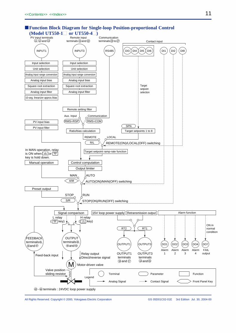
Function Block Diagram for Single-loop Position-proportional Control(Model UT550-1 or UT550-4 )
RMS=COMRMS=RSP
SPN
R/L
Control computationManual operation
Preset output
Signal comparison
AUTO(ON)/MAN(OFF) switching
STOP(ON)/RUN(OFF) switchingS/R
AUTOMAN
RUNSTOP
A/M
OUTPUT1 OUTPUT3
15V loop power supply Retransmission output
RT2 RT1
1716 1514
DO7DO4DO3DO2DO1
Feed-back input
Valve position sliding resistor
Relay output Direct/reverse signal
49 50
48
46 47
45
M
RS485 DI3 DI4 DI5 DI6 DI1 DI2 DI8INPUT1 INPUT3
Output limiter
PV input terminals , and
Remote input terminals and
Communication terminals to 12 1311 2221 2723 Contact input
Input selection
10-seg. linearizer approx./bias
Analog input filter
Square root extraction
Unit selection
Analog input bias
Analog input range conversion
Input selection
Analog input filter
Square root extraction
Unit selection
Analog input bias
Analog input range conversion
Remote setting filter
Target setpoint selection
REMOTE(ON)/LOCAL(OFF) switching
In MAN operation, relay is ON when orkey is hold down.
CommunicationAux. Input
LOCALREMOTE
PV input filter
PV input bias
Ratio/bias calculation
Target setpoint ramp-rate function
Target setpoints 1 to 8
Alarm function
Alarm1
Alarm2
Alarm3
Alarm4
FAILoutput
ON innormalcondition
Terminal Parameter Function
Analog Signal Contact Signal Front Panel Key
Legend
L relay ( key)
H relay ( key)
FEEDBACKterminals ,
and
OUTPUTterminals ,
and
Motor-driven valve
OUTPUT1terminals
and
43 44- terminals : 24VDC loop power supply
OUTPUT3terminals
and
12
All Rights Reserved. Copyright © 2000, Yokogawa Electric Corporation
<<Contents>> <<Index>>
GS 05D01C02-01E 3rd Edition Jul. 30, 2004-00
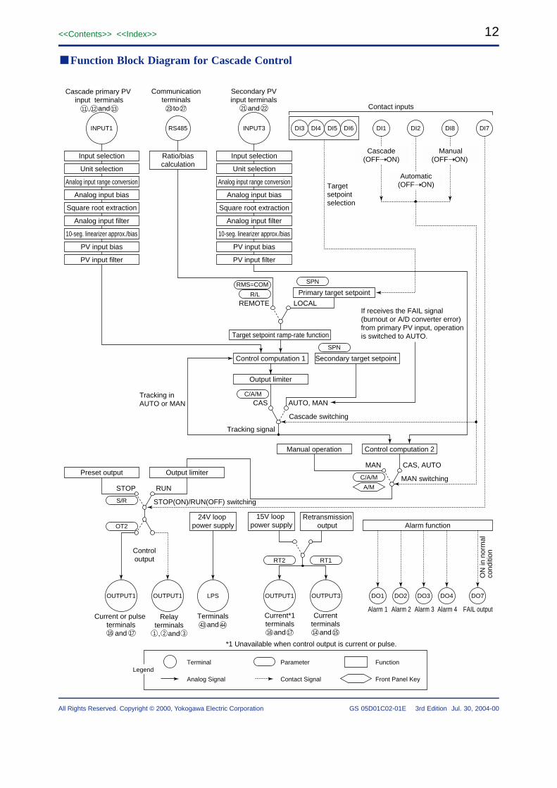
Function Block Diagram for Cascade Control
SPN
R/L
RS485
Control computation 1
Manual operation
Alarm function
Preset outputMAN switching
STOP(ON)/RUN(OFF) switching
OT2
S/R
C/A/M
LOCALREMOTE
C/A/M
SPN
Cascade switching
Tracking signal
Tracking in AUTO or MAN AUTO, MANCAS
CAS, AUTOMAN
RUNSTOP A/M
Target setpoint ramp-rate function
Controloutput
OUTPUT1 LPSOUTPUT1 OUTPUT1 OUTPUT3
15V loop power supply
24V loop power supply
Retransmissionoutput
RT2 RT1
12 1311
1716 2 31
44431514
*1 Unavailable when control output is current or pulse.
DO7DO4DO3DO2DO1
Alarm 1 Alarm 2 Alarm 3 Alarm 4 FAIL output
DI3 DI4 DI5 DI6INPUT1 INPUT3
22212723
Input selection Ratio/biascalculation
Unit selection
Analog input range conversion
Analog input bias
Analog input filter
Square root extraction
Input selection
Unit selection
Analog input range conversion
Analog input bias
Square root extraction
Analog input filter
10-seg. linearizer approx./bias
PV input bias
PV input filter
10-seg. linearizer approx./bias
PV input bias
PV input filter
Output limiter
Contact inputs
DI8 DI7DI1 DI2
Cascade(OFF ON)
Control computation 2
If receives the FAIL signal (burnout or A/D converter error) from primary PV input, operation is switched to AUTO.
RMS=COMPrimary target setpoint
Secondary target setpoint
Output limiter
Cascade primary PV input terminals
, and
Communicationterminals
to
Secondary PVinput terminals
and
Target setpoint selection
Manual(OFF ON)
Automatic(OFF ON)
Current or pulse terminals
and
Relayterminals
, and
Terminalsand
Currentterminals
and1716
Current*1terminals
and
ON
in n
orm
alco
nditi
on
Terminal Parameter Function
Analog Signal Contact Signal Front Panel Key
Legend
13<<Contents>> <<Index>>
All Rights Reserved. Copyright © 2000, Yokogawa Electric Corporation GS 05D01C02-01E 3rd Edition Jul. 30, 2004-00
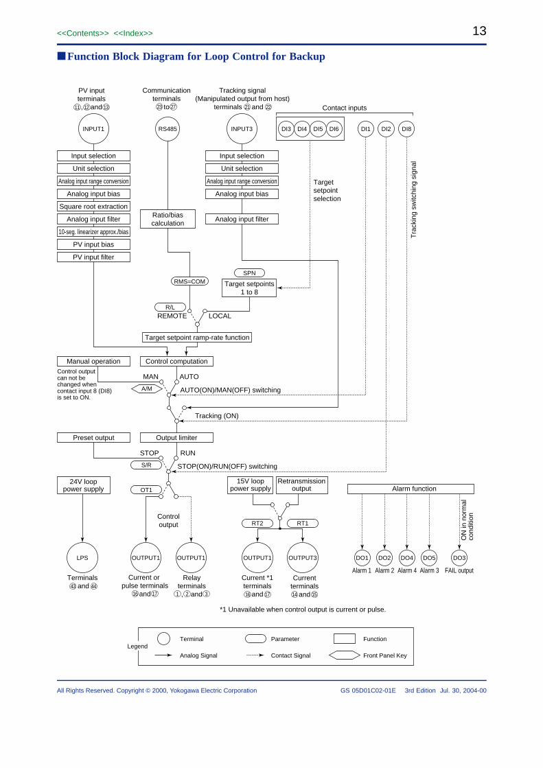
Function Block Diagram for Loop Control for Backup
RS485
Manual operation
Preset output
STOP(ON)/RUN(OFF) switching
OT1
S/R
AUTOMAN
RUNSTOP
A/M
Controloutput
OUTPUT1 OUTPUT1 OUTPUT1 OUTPUT3
15V looppower supply
Retransmissionoutput
RT2 RT1
12 1311
DO3DO5DO4DO2DO1
DI3 DI4 DI5 DI6 DI1 DI2 DI8INPUT1 INPUT3
22212723
Input selection
Unit selection
Analog input range conversion
Analog input bias
Square root extraction
Analog input filter
Input selection
Unit selection
Analog input range conversion
Analog input bias
Analog input filter
10-seg. linearizer approx./bias
PV input bias
PV input filter
Output limiter
Contact inputs
Ratio/biascalculation
RMS=COMSPN
Target setpoints1 to 8
R/L
Control computation
LOCALREMOTE
Target setpoint ramp-rate function
Control output can not be changed when contact input 8 (DI8) is set to ON.
PV inputterminals
, and
Communicationterminals
to
Tracking signal(Manipulated output from host)
terminals and
Targetsetpointselection
AUTO(ON)/MAN(OFF) switching
Tracking (ON)T
rack
ing
switc
hing
sig
nal
1716 2 31 1716 1514
Current or pulse terminals
and
Relayterminals
, and
Current *1terminals
and
Currentterminals
and
*1 Unavailable when control output is current or pulse.
Alarm function
Alarm 1 Alarm 2 Alarm 4 Alarm 3 FAIL output
ON
in n
orm
alco
nditi
on
Terminal Parameter Function
Analog Signal Contact Signal Front Panel Key
Legend
24V looppower supply
Terminals and 4443
LPS
14
All Rights Reserved. Copyright © 2000, Yokogawa Electric Corporation
<<Contents>> <<Index>>
GS 05D01C02-01E 3rd Edition Jul. 30, 2004-00
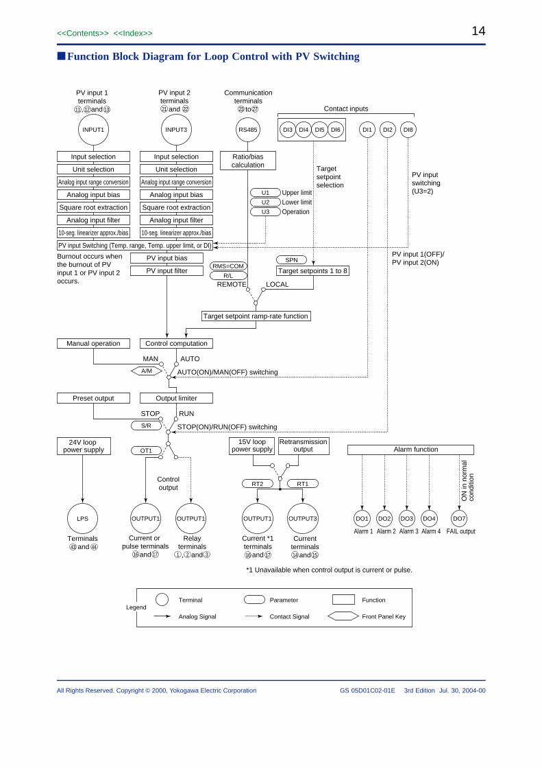
Function Block Diagram for Loop Control with PV Switching
PV input 2terminals
and 22
RS485
Control computationManual operation
Preset output
AUTO(ON)/MAN(OFF) switching
STOP(ON)/RUN(OFF) switching
OT1
S/R
AUTOMAN
RUNSTOP
A/M
Controloutput
OUTPUT1 OUTPUT1 OUTPUT1 OUTPUT3
RT2 RT1
*1 Unavailable when control output is current or pulse.
DO7DO4DO3DO2DO1
DI3 DI4 DI5 DI6 DI1 DI2 DI8INPUT1 INPUT3
Input selection
Unit selection
Analog input range conversion
Analog input bias
Square root extraction
Analog input filter
Input selection
Unit selection
Analog input range conversion
Analog input bias
Square root extraction
Analog input filter
10-seg. linearizer approx./bias 10-seg. linearizer approx./bias
PV input Switching (Temp. range, Temp. upper limit, or DI)
PV input bias
PV input filter
Output limiter
Contact inputs
Ratio/biascalculation
Target setpoints 1 to 8
Upper limit
PV input 1(OFF)/PV input 2(ON)
Lower limitOperation
U1
U2
U3
RMS=COMSPN
R/L
LOCALREMOTE
Target setpoint ramp-rate function
Burnout occurs whenthe burnout of PV input 1 or PV input 2 occurs.
12 1311 21
PV input 1terminals
, and 2723
Communicationterminals
to
Target setpoint selection
PV input switching (U3=2)
1716 2 31 1716 1514
Current or pulse terminals
and
Relayterminals
, and
Current *1terminals
and
Currentterminals
and
15V looppower supply
Retransmissionoutput Alarm function
Alarm 1 Alarm 2 Alarm 3 Alarm 4 FAIL output
ON
in n
orm
alco
nditi
on
Terminal Parameter Function
Analog Signal Contact Signal Front Panel Key
Legend
24V loop power supply
Terminals and 4443
LPS
15<<Contents>> <<Index>>
All Rights Reserved. Copyright © 2000, Yokogawa Electric Corporation GS 05D01C02-01E 3rd Edition Jul. 30, 2004-00
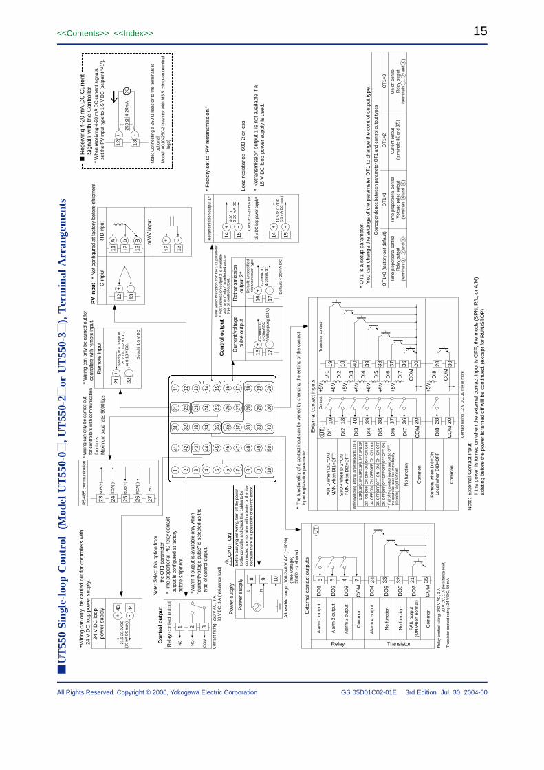
U
T55
0 Si
ngle
-loo
p C
ontr
ol
(Mod
el U
T55
0-0
, UT
550-
2or
UT
550-
3),
Ter
min
al A
rran
gem
ents
1 2 3 4 5 6 7 8 9 10
41 42 43 44 45 46 47 48 49 50
31 32 33 34 35 36 37 38 39 40
21 22 23 24 25 26 27 28 29 30
11 12 13 14 15 16 17 18 19 20
8 9
Pow
er s
uppl
y 10
L N
Allo
wab
le r
ange
: 100
-240
V A
C (
10
%)
(fre
e vo
ltage
) 50
/60
Hz
shar
ed
Pow
er s
uppl
y
12 13
TC
inpu
t
11 12
RTD
inpu
t
13 12 13
mV
/V in
put
21 22
Rem
ote
inpu
t
* W
iring
can
onl
y be
car
ried
out f
or
co
ntro
llers
with
rem
ote
inpu
t.
Spe
cify
in a
ran
ge o
f 1-
5 V
DC
, 0-2
V D
C,
or 0
-10
V D
C.
23 24
RS
-485
com
mun
icat
ion
* W
iring
can
onl
y be
car
ried
out
fo
r con
trolle
rs w
ith c
omm
unic
atio
n
func
tions
.
Max
imum
bau
d ra
te: 9
600
bps
25 26 27
SD
B(+
)
SD
A(-
)
RD
B(+
)
RD
A(-
)
SG
* T
he fu
nctio
nalit
y of
a c
onta
ct in
put c
an b
e va
ried
by c
hang
ing
the
setti
ng o
f the
con
tact
inpu
t reg
istr
atio
n pa
ram
eter
.
* F
acto
ry-s
et to
“P
V r
etra
nsm
issi
on.”
* R
etra
nsm
issi
on o
utpu
t 1 is
not
ava
ilabl
e if
a
15 V
DC
loop
pow
er s
uppl
y is
use
d.
24 V
DC
loop
po
wer
sup
ply
*Wiri
ng c
an o
nly
be
carr
ied
out f
or c
ontr
olle
rs w
ith
24
V D
C lo
op p
ower
sup
ply.
1 2
Rel
ay c
onta
ct o
utpu
t
3
Co
ntr
ol o
utp
ut
NC
NO
CO
M
Con
tact
ratin
g: 2
50 V
AC
, 3 A
30
V D
C, 3
A (r
esis
tanc
e lo
ad)
*Ti
me
prop
ortio
nal P
ID re
lay
cont
act
out
put i
s co
nfig
ured
at f
acto
ry b
efor
e sh
ipm
ent.
Not
e: S
elec
t thi
s op
tion
from
the
OT1
par
amet
er.
CA
UT
ION
Bef
ore
carr
ying
out
wiri
ng, t
urn
off t
he p
ower
to
the
cont
rolle
r and
che
ck th
at c
able
s to
be
conn
ecte
d ar
e no
t aliv
e w
ith a
test
er o
r the
like
be
caus
e th
ere
is a
pos
sibi
lity
of e
lect
ric s
hock
.
A b B
-+
-+
-+
21.6
-28.
0VD
C(3
0 m
A D
C m
ax.)
43 44
+ -
Def
ault:
1-5
V D
C
OT
1=0
(fac
tory
-set
def
ault)
OT
1=1
Cor
resp
onde
nce
betw
een
para
met
er O
T1 a
nd c
ontro
l out
put t
ypes
OT
1=2
OT
1=3
* O
T1
is a
set
up p
aram
eter
.
You
can
cha
nge
the
setti
ngs
of th
e pa
ram
eter
OT
1 to
cha
nge
the
cont
rol o
utpu
t typ
e.
Tim
e pr
opor
tiona
l con
trol
Rel
ay o
utpu
t (te
rmin
als
,
and
)
12
3
Tim
e pr
opor
tiona
l con
trol
Vol
tage
pul
se o
utpu
t (te
rmin
als
a
nd
)
1617
Cur
rent
out
put
(ter
min
als
and
)16
17O
n-of
f con
trol
Rel
ay o
utpu
t (te
rmin
als
,
and
)
12
3
PV
inp
ut
* N
ot c
onfig
ured
at f
acto
ry b
efor
e sh
ipm
ent
19 18
Ext
erna
l con
tact
inpu
ts
40 39 38 37 20 28 30
DI1
DI2
DI3
DI4
DI5
DI6
CO
M
CO
M
DI8
AU
TO
whe
n D
I1=
ON
MA
N w
hen
DI1
=O
FF
ST
OP
whe
n D
I2=
ON
R
UN
whe
n D
I2=
OF
F
DI3
DI4
1.SP
2.SP
3.SP
4.SP
ON
ON
OFF
OFF
ON
ON
OFF
OFF
5.SP
6.SP
7.SP
8.SP
ON
ON
OFF
OFF
ON
ON
OFF
OFF
DI5
DI6
OFF
OFF
OFF
OFF
OFF
OFF
ON
OFF
ON
OFF
ON
OFF
ON
OFF
OFF ON
Com
mon
Rem
ote
whe
n D
I8=
ON
Loc
al w
hen
DI8
=O
FF
Com
mon
Whe
n sw
itchi
ng a
mon
g ta
rget
set
poin
ts 1
to 8
:
19 18 40 39 38 37 20 28 30
DI1
DI2
DI3
DI4
DI5
DI6
CO
M
CO
M
DI8
+5V
+5V
+5V
+5V
+5V
+5V
36D
I736
DI7
+5V
+5V
Con
tact
T
rans
isto
r co
ntac
t
Con
tact
rat
ing:
12
V D
C, 1
0 m
A o
r m
ore
No
func
tion
16 17
Cur
rent
/vol
tage
pu
lse
outp
ut
0-20
mA
DC
,4-
20m
AD
CV
olta
ge p
ulse
(12
V)
Co
ntr
ol o
utp
ut
14 15
Ret
rans
mis
sion
out
put 1
*
4-20
or
0-20
mA
DC
14 1515 V
DC
loop
pow
er s
uppl
y*
14.5
-18.
0 V
DC
(21
mA
DC
max
.)
* R
etra
nsm
issi
on o
utpu
t 2 is
ava
ilabl
e
only
whe
n “r
elay
” is
sel
ecte
d as
the
ty
pe o
f con
trol
out
put.
16 17Ret
rans
mis
sion
ou
tput
2*
Def
ault:
4-2
0 m
A D
C
Def
ault:
4-2
0 m
A D
C
0-20
mA
DC
,4-
20m
AD
C
UT
* If
all o
f the
con
tact
inpu
ts a
re s
et to
OFF
,
the
cont
rolle
r use
s th
e im
med
iate
ly
pr
eced
ing
targ
et s
etpo
int.
-+
-+
-+ -+
6 5
Ext
erna
l con
tact
out
puts
4 7 34 33
DO
1
DO
2
DO
3
CO
M
DO
4
DO
5
Relay Transistor
No
func
tion
Ala
rm 1
out
put
Ala
rm 2
out
put
Ala
rm 3
out
put
Com
mon
Ala
rm 4
out
put
32D
O6
31D
O7
35C
OM
No
func
tion
Com
mon
UT
FA
IL o
utpu
t(O
N w
hen
norm
al)
Rel
ay c
onta
ct r
atin
g: 2
40 V
AC
, 1 A
30 V
DC
, 1 A
(re
sist
ance
load
) T
rans
isto
r co
ntac
t rat
ing:
24
V D
C, 5
0 m
A
Load
res
ista
nce:
600
Ω o
r les
s
12 13
Not
e: C
onne
ctin
g a
250
Ω re
sist
or to
the
term
inal
s is
opt
iona
l.M
odel
: X01
0-25
0-2
(res
isto
r with
M3.
5 cr
imp-
on te
rmin
al
lugs
)
* W
hen
rece
ivin
g 4-
20 m
A D
C c
urre
nt s
igna
ls,
se
t the
PV
inpu
t typ
e to
1-5
V D
C (s
etpo
int “
41”)
.
R
ecei
ving
4-2
0 m
A D
C C
urre
nt
S
igna
ls w
ith th
e C
ontr
olle
r
250
Ω4-
20m
A
-+
Def
ault:
Uns
peci
fied
retr
ansm
issi
on ty
pe
Not
e: S
elec
t thi
s op
tion
from
the
OT1
par
amet
er.
Not
e: E
xter
nal C
onta
ct In
put
If
the
pow
er is
turn
ed o
n w
hen
the
exte
rnal
con
tact
inpu
t is
OF
F, t
he m
ode
(SP
N, R
/L, o
r A
/M)
ex
istin
g be
fore
the
pow
er is
turn
ed o
ff w
ill b
e co
ntin
ued.
(ex
cept
for
RU
N/S
TO
P)
*Ala
rm 4
out
put i
s av
aila
ble
only
whe
n "c
urre
nt/v
olta
ge p
ulse
" is
sele
cted
as
the
type
of c
ontro
l out
put.
16
All Rights Reserved. Copyright © 2000, Yokogawa Electric Corporation
<<Contents>> <<Index>>
GS 05D01C02-01E 3rd Edition Jul. 30, 2004-00
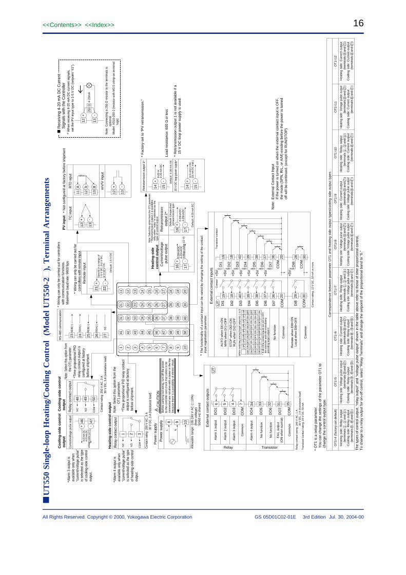
U
T55
0 Si
ngle
-loo
p H
eati
ng/C
oolin
g C
ontr
ol
(Mod
el U
T55
0-2
), T
erm
inal
Arr
ange
men
ts
1 2 3 4 5 6 7 8 9 10
41 42 43 44 45 46 47 48 49 50
31 32 33 34 35 36 37 38 39 40
21 22 23 24 25 26 27 28 29 30
11 12 13 14 15 16 17 18 19 20
Hea
tin
g-s
ide
con
tro
l ou
tpu
t
Cur
rent
/vol
tage
pul
se o
utpu
t
Co
olin
g-s
ide
con
tro
l o
utp
ut
Co
olin
g-s
ide
con
tro
l o
utp
ut
12 13
11 12 13 12 13
A b B
23 24 25 26 27
SD
B(+
)
SD
A(-
)
RD
B(+
)
RD
A(-
)
SG
8 9 10
L N
1 2 3
NC
NO
CO
M
48 49 50
NC
NO
CO
M
+ -
+ -
CA
UT
ION
Bef
ore
carr
ying
out
wiri
ng, t
urn
off t
he p
ower
to
the
cont
rolle
r and
che
ck th
at c
able
s to
be
conn
ecte
d ar
e no
t aliv
e w
ith a
test
er o
r the
like
be
caus
e th
ere
is a
pos
sibi
lity
of e
lect
ric s
hock
.
Pow
er s
uppl
y
Pow
er s
uppl
y
Rel
ay c
onta
ct o
utpu
t
Con
tact
ratin
g: 2
50 V
AC
, 3 A
30
V D
C, 3
A (r
esis
tanc
e lo
ad)
Con
tact
ratin
g: 2
50 V
AC
, 3 A
30
V D
C, 3
A (r
esis
tanc
e lo
ad)
*Ti
me
prop
ortio
nal P
ID re
lay
cont
act
out
put i
s co
nfig
ured
at f
acto
ry b
efor
e sh
ipm
ent.
*Ti
me
prop
ortio
nal P
ID
rel
ay c
onta
ct o
utpu
t is
con
figur
ed a
t fac
tory
bef
ore
ship
men
t.
* W
iring
can
onl
y be
car
ried
out f
or c
ontro
llers
with
com
mun
icat
ion
func
tions
.
Max
imum
bau
d ra
te: 9
600
bps
* W
iring
can
onl
y be
car
ried
out f
or
co
ntro
llers
with
rem
ote
inpu
t.
TC
inpu
tR
TD in
put
mV
/V in
put
21 22
Rem
ote
inpu
t
Spe
cify
in a
ran
ge o
f 1-
5 V
DC
, 0-2
V D
C,
or 0
-10
V D
C.
-+
RS
-485
com
mun
icat
ion
Rel
ay c
onta
ct o
utpu
t
Def
ault:
1-5
V D
C
OT
1=4
(fac
tory
-set
def
ault)
OT
1=5
Cor
resp
onde
nce
betw
een
para
met
er O
T1
and
heat
ing
side
out
put
type
s/co
olin
g si
de o
utpu
t ty
pes
OT
1=6
OT
1=7
OT
1=8
OT
1=9
OT
1=10
OT
1=11
OT
1=12
The
type
s of
con
trol
out
put,
“rel
ay o
utpu
t” a
nd “
volta
ge p
ulse
out
put”
sho
wn
in th
e ta
ble
abov
e re
fer
to th
ose
of ti
me
prop
ortio
nal c
ontr
ol.
To
chan
ge to
a r
elay
out
put f
or o
n-of
f con
trol
, sel
ect “
Rel
ay T
erm
inal
s” a
nd c
hang
e th
e se
tpoi
nt o
f the
pro
port
iona
l ban
d to
“0.
”
Hea
ting
side
: R
elay
out
put
(t
erm
inal
s
,
an
d
)C
oolin
g si
de:
Rel
ay o
utpu
t
(ter
min
als
,
and
)
12
3H
eatin
g si
de: V
olta
ge p
ulse
out
put
(t
erm
inal
s
and
)C
oolin
g si
de:
Rel
ay o
utpu
t
(ter
min
als
,
and
)
1617
Hea
ting
side
: C
urre
nt o
utpu
t
(ter
min
als
a
nd
)
Coo
ling
side
: R
elay
out
put
(t
erm
inal
s
,
an
d
)
1617
Hea
ting
side
: R
elay
out
put
(t
erm
inal
s
,
an
d
)C
oolin
g si
de: V
olta
ge p
ulse
out
put
(t
erm
inal
s
and
)
12
3H
eatin
g si
de:
Rel
ay o
utpu
t
(ter
min
als
,
and
)
Coo
ling
side
: C
urre
nt o
utpu
t
(ter
min
als
a
nd
)
12
3H
eatin
g si
de: V
olta
ge p
ulse
out
put
(t
erm
inal
s
and
)C
oolin
g si
de: V
olta
ge p
ulse
out
put
(t
erm
inal
s
and
)
1617
Hea
ting
side
: C
urre
nt o
utpu
t
(ter
min
als
a
nd
)
Coo
ling
side
: Vol
tage
pul
se o
utpu
t
(ter
min
als
a
nd
)
1617
Hea
ting
side
: Vol
tage
pul
se o
utpu
t
(ter
min
als
a
nd
)
Coo
ling
side
: C
urre
nt o
utpu
t
(ter
min
als
a
nd
)
1617
Hea
ting
side
: C
urre
nt o
utpu
t
(ter
min
als
a
nd
)
Coo
ling
side
: C
urre
nt o
utpu
t
(ter
min
als
a
nd
)
1617
* F
acto
ry-s
et to
“P
V r
etra
nsm
issi
on.”
* R
etra
nsm
issi
on o
utpu
t 1 is
not
ava
ilabl
e if
a
15 V
DC
loop
pow
er s
uppl
y is
use
d.
Hea
tin
g-s
ide
con
tro
l ou
tpu
t14 15
Ret
rans
mis
sion
out
put 1
*
4-20
or
0-20
mA
DC
14 15
15 V
DC
loop
pow
er s
uppl
y*
14.5
-18.
0 V
DC
(21
mA
DC
max
.)
* R
etra
nsm
issi
on o
utpu
t 2 is
ava
ilabl
e
only
whe
n “r
elay
” is
sel
ecte
d as
the
ty
pe o
f con
trol
out
put.
Def
ault:
4-2
0 m
A D
C
-+ -+
* T
he fu
nctio
nalit
y of
a c
onta
ct in
put c
an b
e va
ried
by c
hang
ing
the
setti
ng o
f the
con
tact
inpu
t reg
istr
atio
n pa
ram
eter
.
* O
T1
is a
set
up p
aram
eter
.
You
can
cha
nge
the
setti
ngs
of th
e pa
ram
eter
OT
1 to
chan
ge th
e co
ntro
l out
put t
ype.
19 18
Ext
erna
l con
tact
inpu
ts
40 39 38 37 20 28 30
DI1
DI2
DI3
DI4
DI5
DI6
CO
M
CO
M
DI8
AU
TO
whe
n D
I1=
ON
MA
N w
hen
DI1
=O
FF
ST
OP
whe
n D
I2=
ON
R
UN
whe
n D
I2=
OF
F
DI3
DI4
1.SP
2.SP
3.SP
4.SP
ON
ON
OFF
OFF
ON
ON
OFF
OFF
5.SP
6.SP
7.SP
8.SP
ON
ON
OFF
OFF
ON
ON
OFF
OFF
DI5
DI6
OFF
OFF
OFF
OFF
OFF
OFF
ON
OFF
ON
OFF
ON
OFF
ON
OFF
OFF ON
Com
mon
Rem
ote
whe
n D
I8=
ON
Loc
al w
hen
DI8
=O
FF
Com
mon
Whe
n sw
itchi
ng a
mon
g ta
rget
set
poin
ts 1
to 8
:
19 18 40 39 38 37 20 28 30
DI1
DI2
DI3
DI4
DI5
DI6
CO
M
CO
M
DI8
+5V
+5V
+5V
+5V
+5V
+5V
36D
I736
DI7
+5V
+5V
Con
tact
T
rans
isto
r co
ntac
t
Con
tact
rat
ing:
12
V D
C, 1
0 m
A o
r m
ore
No
func
tion
UT
* If
all o
f the
con
tact
inpu
ts a
re s
et to
OFF
,
the
cont
rolle
r use
s th
e im
med
iate
ly
pr
eced
ing
targ
et s
etpo
int.
6 5
Ext
erna
l con
tact
out
puts
4 7 34 33
DO
1
DO
2
DO
3
CO
M
DO
4
DO
5N
o fu
nctio
n
Ala
rm 1
out
put
Ala
rm 2
out
put
Ala
rm 3
out
put
Com
mon
Ala
rm 4
out
put
32D
O6
31D
O7
35C
OM
No
func
tion
Com
mon
UT
FA
IL o
utpu
t(O
N w
hen
norm
al)
Rel
ay c
onta
ct r
atin
g: 2
40 V
AC
, 1 A
30 V
DC
, 1 A
(re
sist
ance
load
) T
rans
isto
r co
ntac
t rat
ing:
24
V D
C, 5
0 m
A
4847
4647
4647
4647
4647
4647
4649
5048
4950
4849
50
46 47
+ -
0-20
mA
DC
4-
20 m
A D
C,
volta
ge p
ulse
(12
V)
PV
inp
ut
16 17
Cur
rent
/vol
tage
pu
lse
outp
ut
0-20
mA
DC
,4-
20m
AD
CV
olta
ge p
ulse
(12
V)
16 17Ret
rans
mis
sion
ou
tput
2*
Def
ault:
4-2
0 m
A D
C
0-20
mA
DC
,4-
20m
AD
C-+
-+
Allo
wab
le r
ange
: 100
-240
V A
C (
10
%)
(fre
e vo
ltage
) 50
/60
Hz
shar
ed
Load
res
ista
nce:
600
Ω o
r le
ss
12 13
Not
e: C
onne
ctin
g a
250
Ω r
esis
tor
to th
e te
rmin
als
is
o
ptio
nal.
Mod
el: X
010-
250-
2 (r
esis
tor
with
M3.
5 cr
imp-
on te
rmin
al
lugs
)
* W
hen
rece
ivin
g 4-
20 m
A D
C c
urre
nt s
igna
ls,
se
t the
PV
inpu
t typ
e to
1-5
V D
C (
setp
oint
“41
”).
R
ecei
ving
4-2
0 m
A D
C C
urre
nt
S
igna
ls w
ith th
e C
ontr
olle
r
250
Ω4-
20m
A
-+
* N
ot c
onfig
ured
at f
acto
ry b
efor
e sh
ipm
ent
Def
ault:
Uns
peci
fied
retr
ansm
issi
on ty
pe
Note
: Sel
ect t
his
optio
n fro
m
th
e O
T1 p
aram
eter
.
Not
e: S
elec
t thi
s op
tion
from
the
O
T1 p
aram
eter
.
Not
e: S
elec
t thi
s op
tion
from
the
OT1
par
amet
er.
Not
e: E
xter
nal C
onta
ct In
put
If
the
pow
er is
turn
ed o
n w
hen
the
exte
rnal
con
tact
inpu
t is
OF
F,
th
e m
ode
(SP
N, R
/L, o
r A
/M)
exis
ting
befo
re th
e po
wer
is tu
rned
off w
ill b
e co
ntin
ued.
(ex
cept
for
RU
N/S
TO
P)
Relay Transistor
*Ala
rm 3
out
put i
s a
vaila
ble
only
whe
n "c
urre
nt/v
olta
ge p
ulse
" is
sel
ecte
d as
the
type
of c
oolin
g-si
de c
ontro
l o
utpu
t.
*Ala
rm 4
out
put i
s a
vaila
ble
only
whe
n "c
urre
nt/v
olta
ge p
ulse
" is
sel
ecte
d as
the
type
of h
eatin
g-si
de c
ontro
l o
utpu
t.
17<<Contents>> <<Index>>
All Rights Reserved. Copyright © 2000, Yokogawa Electric Corporation GS 05D01C02-01E 3rd Edition Jul. 30, 2004-00
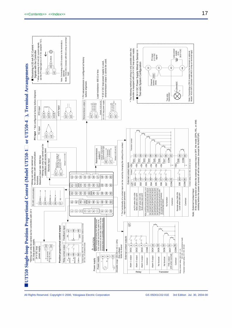
U
T55
0 Si
ngle
-loo
p P
osit
ion
Pro
port
iona
l C
ontr
ol (
Mod
el U
T55
0-1
or
UT
550-
4),
Ter
min
al A
rran
gem
ents
1 2 3 4 5 6 7 8 9 10
41 42 43 44 45 46 47 48 49 50
31 32 33 34 35 36 37 38 39 40
21 22 23 24 25 26 27 28 29 30
11 12 13 14 15 16 17 18 19 20
Fee
dbac
k in
put
Res
ista
nce:
100
to
2.5
k
Po
siti
on
pro
po
rtio
nal
co
ntr
ol o
utp
ut
48 49
Rel
ay c
onta
ct o
utpu
t
50
H(D
irect
)
L (R
ever
se)
CO
M
Con
tact
rat
ing:
250
V A
C, 3
A
30
V D
C, 3
A (
resi
stan
ce lo
ad)
8 9 10
L N
23 24
* W
iring
can
onl
y be
car
ried
out
fo
r co
ntro
llers
with
com
mun
icat
ion
fu
nctio
ns.
M
axim
um b
aud
rate
: 960
0 bp
s
25 26 27
SD
B(+
)
SD
A(-
)
RD
B(+
)
RD
A(-
)
SG
12 13
11 12 13 12 13 14 15 14 15
A b B
24 V
DC
loop
po
wer
sup
ply
*Wiri
ng c
an o
nly
be c
arrie
d ou
t for
con
trol
lers
with
24
V
D
C lo
op p
ower
sup
ply.
Pow
er s
uppl
y
Pow
er s
uppl
y C
AU
TIO
NB
efor
e ca
rryi
ng o
ut w
iring
, tur
n of
f the
pow
er
to th
e co
ntro
ller a
nd c
heck
that
cab
les
to b
e co
nnec
ted
are
not a
live
with
a te
ster
or t
he li
ke
beca
use
ther
e is
a p
ossi
bilit
y of
ele
ctric
sho
ck.
+ -
+ -
+ -+ -
Ret
rans
mis
sion
out
put 1
15
V D
C lo
op p
ower
sup
ply
14.5
-18.
0VD
C(2
1 m
A D
C m
ax.)
* P
V r
etra
nsm
issi
on is
con
figur
ed a
t fac
tory
be
fore
shi
pmen
t.
* If
15 V
DC
loop
pow
er s
uppl
y is
use
d,
ret
rans
mis
sion
out
put 1
can
not b
e us
ed.
21 22
Rem
ote
inpu
t
* W
iring
can
onl
y be
car
ried
out f
or
co
ntro
llers
with
rem
ote
inpu
t.
Spe
cify
in a
ran
ge o
f 1-
5 V
DC
, 0-2
V D
C,
or 0
-10
V D
C.
-+
RS
-485
com
mun
icat
ion
TC
inpu
tR
TD in
put
mV
/V in
put
21.6
-28.
0VD
C(3
0 m
A D
C m
ax.)
43 44
+ -
Def
ault:
1-5
V D
C
0%
100%
47 46 45
* T
he fu
nctio
nalit
y of
a c
onta
ct in
put c
an b
e va
ried
by c
hang
ing
the
setti
ng o
f the
con
tact
inpu
t reg
istr
atio
n pa
ram
eter
.
19 18
Ext
erna
l con
tact
inpu
ts
40 39 38 37 20 28 30
DI1
DI2
DI3
DI4
DI5
DI6
CO
M
CO
M
DI8
AU
TO
whe
n D
I1=
ON
MA
N w
hen
DI1
=O
FF
ST
OP
whe
n D
I2=
ON
R
UN
whe
n D
I2=
OF
F
DI3
DI4
1.SP
2.SP
3.SP
4.SP
ON
ON
OFF
OFF
ON
ON
OFF
OFF
5.SP
6.SP
7.SP
8.SP
ON
ON
OFF
OFF
ON
ON
OFF
OFF
DI5
DI6
OFF
OFF
OFF
OFF
OFF
OFF
ON
OFF
ON
OFF
ON
OFF
ON
OFF
OFF ON
Com
mon
Rem
ote
whe
n D
I8=
ON
Loc
al w
hen
DI8
=O
FF
Com
mon
Whe
n sw
itchi
ng a
mon
g ta
rget
set
poin
ts 1
to 8
:
19 18 40 39 38 37 20 28 30
DI1
DI2
DI3
DI4
DI5
DI6
CO
M
CO
M
DI8
+5V
+5V
+5V
+5V
+5V
+5V
36D
I736
DI7
+5V
+5V
Con
tact
T
rans
isto
r co
ntac
t
Con
tact
rat
ing:
12
V D
C, 1
0 m
A o
r m
ore
No
func
tion
UT
* If
all o
f the
con
tact
inpu
ts a
re s
et to
OFF
,
the
cont
rolle
r use
s th
e im
med
iate
ly
pr
eced
ing
targ
et s
etpo
int.
6 5
Ext
erna
l con
tact
out
puts
4 7 34 33
DO
1
DO
2
DO
3
CO
M
DO
4
DO
5
Relay Transistor
No
func
tion
Ala
rm 1
out
put
Ala
rm 2
out
put
Ala
rm 3
out
put
Com
mon
Ala
rm 4
out
put
32D
O6
31D
O7
35C
OM
No
func
tion
Com
mon
UT
FA
IL o
utpu
t(O
N w
hen
norm
al)
Rel
ay c
onta
ct r
atin
g: 2
40 V
AC
, 1 A
30 V
DC
, 1 A
(re
sist
ance
load
) T
rans
isto
r co
ntac
t rat
ing:
24
V D
C, 5
0 m
A
PV
inp
ut
Allo
wab
le r
ange
: 100
-240
V A
C (
10
%)
(fre
e vo
ltage
) 50
/60
Hz
shar
ed
* N
ot c
onfig
ured
at f
acto
ry b
efor
e sh
ipm
ent
12 13
Not
e: C
onne
ctin
g a
250
Ω r
esis
tor
to th
e te
rmin
als
is
o
ptio
nal.
Mod
el: X
010-
250-
2 (r
esis
tor
with
M3.
5 cr
imp-
on te
rmin
al
lugs
)
* W
hen
rece
ivin
g 4-
20 m
A D
C c
urre
nt s
igna
ls,
se
t the
PV
inpu
t typ
e to
1-5
V D
C (
setp
oint
“41
”).
R
ecei
ving
4-2
0 m
A D
C C
urre
nt
S
igna
ls w
ith th
e C
ontr
olle
r
250
Ω4-
20m
A
-+
16 17Ret
rans
mis
sion
ou
tput
2
Def
ault:
4-2
0 m
A D
C
0-20
mA
DC
,4-
20m
AD
C
Def
ault:
4-2
0 m
A D
C
4-20
mA
DC
,0-
20 m
A D
C
-+Def
ault:
Uns
peci
fied
retr
ansm
issi
on ty
pe
Load
res
ista
nce:
600
Ω o
r le
ss
2
4 V
DC
Pow
er S
uppl
y W
ired
to S
enso
r in
Tw
o-w
ire S
yste
m C
onfig
urat
ion
12 13 43 44
250
Tw
o-w
ire
tran
smitt
er
PV
inpu
t1-
5 V
DC
sign
al
Loop
pow
er
supp
ly 2
1.6-
28
.0 V
DC
Ext
erna
lre
sist
or (N
ote)
Not
e: C
onne
ctin
g a
250
r
esis
tor
to th
e te
rmin
als
is o
ptio
nal.
Mod
el: X
010-
250-
2 (r
esis
tor
with
M3.
5 cr
imp-
on te
rmin
al lu
gs)
* T
he fo
llow
ing
met
hod
of w
iring
is o
nly
poss
ible
whe
n th
e
cont
rolle
r is
equ
ippe
d w
ith a
24
V D
C lo
op p
ower
sup
ply.
4-20
mA
DC
Not
e: E
xter
nal C
onta
ct In
put
If
the
pow
er is
turn
ed o
n w
hen
the
exte
rnal
con
tact
inpu
t is
OF
F, t
he m
ode
(SP
N, R
/L, o
r A
/M)
ex
istin
g be
fore
the
pow
er is
turn
ed o
ff w
ill b
e co
ntin
ued.
(ex
cept
for
RU
N/S
TO
P)
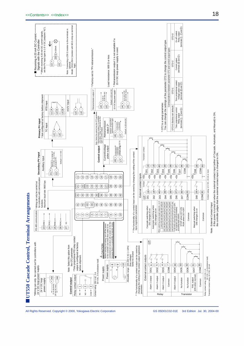
18
All Rights Reserved. Copyright © 2000, Yokogawa Electric Corporation
<<Contents>> <<Index>>
GS 05D01C02-01E 3rd Edition Jul. 30, 2004-00
U
T55
0 C
asca
de C
ontr
ol, T
erm
inal
Arr
ange
men
ts
1 2 3 4 5 6 7 8 9 10
41 42 43 44 45 46 47 48 49 50
31 32 33 34 35 36 37 38 39 40
21 22 23 24 25 26 27 28 29 30
11 12 13 14 15 16 17 18 19 20
8 9
Pow
er s
uppl
y 10
L N
Allo
wab
le r
ange
: 100
-240
V A
C (
10
%)
(fre
e vo
ltage
) 50
/60
Hz
shar
ed
Pow
er s
uppl
y
12 13
TC
inpu
t
11 12
RTD
inpu
t
13 12 13
mV
/V in
put
21 22
Aux
iliar
y in
put
Sec
on
dar
y P
V in
pu
t
Spe
cify
in a
ran
ge o
f 1-
5 V
DC
, 0-2
V D
C,
or 0
-10
V D
C.
23 24
RS
-485
com
mun
icat
ion
* W
iring
can
onl
y be
car
ried
out
fo
r con
trolle
rs w
ith c
omm
unic
atio
n
func
tions
.
Max
imum
bau
d ra
te: 9
600
bps
25 26 27
SD
B(+
)
SD
A(-
)
RD
B(+
)
RD
A(-
)
SG
* T
he fu
nctio
nalit
y of
a c
onta
ct in
put c
an b
e va
ried
by c
hang
ing
the
setti
ng o
f the
con
tact
inpu
t reg
istr
atio
n pa
ram
eter
.*
The
func
tiona
lity
of a
con
tact
out
put c
an b
e va
ried
by
ch
angi
ng th
e se
tting
of t
he c
onta
ct o
utpu
t reg
istr
atio
n
para
met
er.
* F
acto
ry-s
et to
“P
V r
etra
nsm
issi
on.”
* R
etra
nsm
issi
on o
utpu
t 1 is
not
ava
ilabl
e if
a
15 V
DC
loop
pow
er s
uppl
y is
use
d.
24 V
DC
loop
po
wer
sup
ply
*Wiri
ng c
an o
nly
be
carr
ied
out f
or c
ontr
olle
rs w
ith
24
V D
C lo
op p
ower
sup
ply.
1 2
Rel
ay c
onta
ct o
utpu
t
3
Co
ntr
ol o
utp
ut
NC
NO
CO
M
Con
tact
ratin
g: 2
50 V
AC
, 3 A
30
V D
C, 3
A (r
esis
tanc
e lo
ad)
*Ti
me
prop
ortio
nal P
ID re
lay
cont
act
out
put i
s co
nfig
ured
at f
acto
ry b
efor
e sh
ipm
ent.
Not
e: S
elec
t thi
s op
tion
from
the
OT2
par
amet
er.
CA
UT
ION
Bef
ore
carr
ying
out
wiri
ng, t
urn
off t
he p
ower
to
the
cont
rolle
r and
che
ck th
at c
able
s to
be
conn
ecte
d ar
e no
t aliv
e w
ith a
test
er o
r the
like
be
caus
e th
ere
is a
pos
sibi
lity
of e
lect
ric s
hock
.
A b B
-+
-+
-+
21.6
-28.
0VD
C(3
0 m
A D
C m
ax.)
43 44
+ -
Def
ault:
1-5
V D
C
OT
2=0
(fac
tory
-set
def
ault)
OT
2=1
Cor
resp
onde
nce
betw
een
para
met
er O
T2 a
nd c
ontro
l out
put t
ypes
OT
2=2
OT
2=3
* O
T2
is a
set
up p
aram
eter
.
You
can
cha
nge
the
setti
ngs
of th
e pa
ram
eter
OT
2 to
cha
nge
the
cont
rol o
utpu
t typ
e.
Tim
e pr
opor
tiona
l con
trol
Rel
ay o
utpu
t (te
rmin
als
,
and
)
12
3
Tim
e pr
opor
tiona
l con
trol
Vol
tage
pul
se o
utpu
t (te
rmin
als
a
nd
)
1617
Cur
rent
out
put
(ter
min
als
and
)16
17O
n-of
f con
trol
Rel
ay o
utpu
t (te
rmin
als
,
and
)
12
3
Pri
mar
y P
V in
pu
t*
Not
con
figur
ed a
t fac
tory
bef
ore
ship
men
t
19 18
Ext
erna
l con
tact
inpu
ts
40 39 38 37 20 28 30
DI1
DI2
DI3
DI4
DI5
DI6
CO
M
CO
M
DI8
Cas
cade
sw
itchi
ng w
hen
DI1
cha
nges
to o
n
Aut
omat
ic s
witc
hing
whe
n D
I2 c
hang
es to
on
DI3
DI4
1.SP
2.SP
3.SP
4.SP
ON
ON
OFF
OFF
ON
ON
OFF
OFF
5.SP
6.SP
7.SP
8.SP
ON
ON
OFF
OFF
ON
ON
OFF
OFF
DI5
DI6
OFF
OFF
OFF
OFF
OFF
OFF
ON
OFF
ON
OFF
ON
OFF
ON
OFF
OFF ON
Com
mon
Man
ual s
witc
hing
whe
n D
I8 c
hang
es to
on
Com
mon
Whe
n sw
itchi
ng a
mon
g ta
rget
set
poin
ts 1
to 8
:
19 18 40 39 38 37 20 28 30
DI1
DI2
DI3
DI4
DI5
DI6
CO
M
CO
M
DI8
+5V
+5V
+5V
+5V
+5V
+5V
36D
I736
DI7
+5V
+5V
Con
tact
T
rans
isto
r co
ntac
t
Con
tact
rat
ing:
12
V D
C, 1
0 m
A o
r m
ore
ST
OP
whe
n D
I7=
ON
RU
N w
hen
DI7
=O
FF
16 17
Cur
rent
/vol
tage
pu
lse
outp
ut
0-20
mA
DC
,4-
20m
AD
CV
olta
ge p
ulse
(12
V)
Co
ntr
ol o
utp
ut
14 15
Ret
rans
mis
sion
out
put 1
*
4-20
or
0-20
mA
DC
14 1515 V
DC
loop
pow
er s
uppl
y*
14.5
-18.
0 V
DC
(21
mA
DC
max
.)
* R
etra
nsm
issi
on o
utpu
t 2 is
ava
ilabl
e
only
whe
n “r
elay
” is
sel
ecte
d as
the
ty
pe o
f con
trol
out
put.
16 17Ret
rans
mis
sion
ou
tput
2*
Def
ault:
4-2
0 m
A D
C
Def
ault:
4-2
0 m
A D
C
0-20
mA
DC
,4-
20m
AD
C
UT
* If
all o
f the
con
tact
inpu
ts a
re s
et to
OFF
,
the
cont
rolle
r use
s th
e im
med
iate
ly
pr
eced
ing
targ
et s
etpo
int.
-+
-+
-+ -+
6 5
Ext
erna
l con
tact
out
puts
4 7 34 33
DO
1
DO
2
DO
3
CO
M
DO
4
DO
5
Relay Transistor
No
func
tion
Ala
rm 1
out
put
Ala
rm 2
out
put
Ala
rm 3
out
put
Com
mon
Ala
rm 4
out
put
32D
O6
31D
O7
35C
OM
No
func
tion
Com
mon
UT
FA
IL o
utpu
t(O
N w
hen
norm
al)
Rel
ay c
onta
ct r
atin
g: 2
40 V
AC
, 1 A
30 V
DC
, 1 A
(re
sist
ance
load
) T
rans
isto
r co
ntac
t rat
ing:
24
V D
C, 5
0 m
A
Load
res
ista
nce:
600
Ω o
r le
ss
12 13
Not
e: C
onne
ctin
g a
250
Ω r
esis
tor
to th
e te
rmin
als
is
o
ptio
nal.
Mod
el: X
010-
250-
2 (r
esis
tor
with
M3.
5 cr
imp-
on te
rmin
al
lugs
)
* W
hen
rece
ivin
g 4-
20 m
A D
C c
urre
nt s
igna
ls,
se
t the
PV
inpu
t typ
e to
1-5
V D
C (
setp
oint
“41
”).
R
ecei
ving
4-2
0 m
A D
C C
urre
nt
S
igna
ls w
ith th
e C
ontr
olle
r
250
Ω4-
20m
A
-+
Def
ault:
Uns
peci
fied
retr
ansm
issi
on ty
pe
Not
e: S
elec
t thi
s op
tion
from
the
OT2
par
amet
er.
Not
e: E
xter
nal C
onta
ct In
put
If
the
pow
er is
turn
ed o
n w
hen
the
exte
rnal
con
tact
inpu
t (ei
ther
of C
asca
de, A
utom
atic
, and
Man
ual)
is O
N,
th
e co
ntro
ller
judg
es th
at th
e ex
tern
al c
onta
ct in
put i
s ch
ange
d to
ON
.
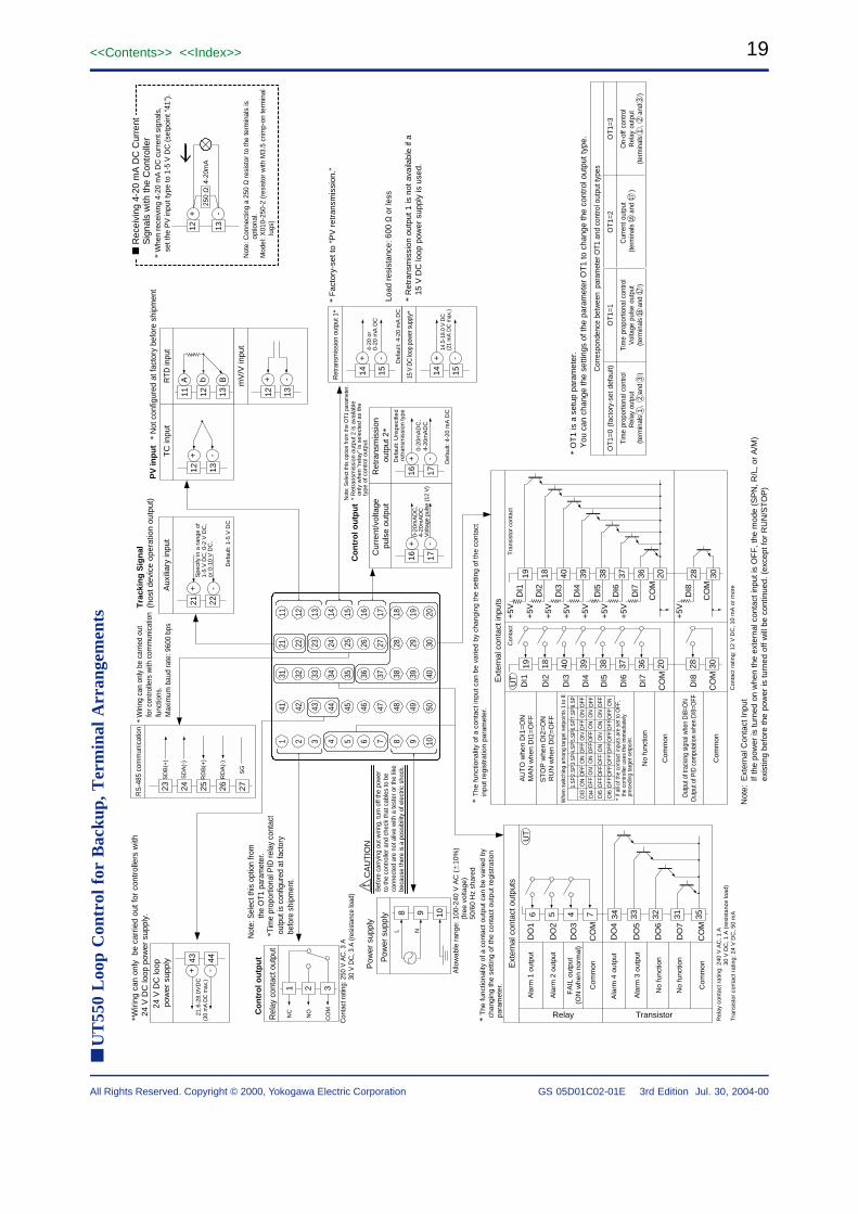
19<<Contents>> <<Index>>
All Rights Reserved. Copyright © 2000, Yokogawa Electric Corporation GS 05D01C02-01E 3rd Edition Jul. 30, 2004-00
U
T55
0 L
oop
Con
trol
for
Bac
kup,
Ter
min
al A
rran
gem
ents
1 2 3 4 5 6 7 8 9 10
41 42 43 44 45 46 47 48 49 50
31 32 33 34 35 36 37 38 39 40
21 22 23 24 25 26 27 28 29 30
11 12 13 14 15 16 17 18 19 20
8 9
Pow
er s
uppl
y 10
L N
Allo
wab
le r
ange
: 100
-240
V A
C (
10
%)
(fre
e vo
ltage
) 50
/60
Hz
shar
ed
Pow
er s
uppl
y
12 13
TC
inpu
t
11 12
RTD
inpu
t
13 12 13
mV
/V in
put
21 22
Aux
iliar
y in
put
Tra
ckin
g S
ign
al
(hos
t dev
ice
oper
atio
n ou
tput
)
Spe
cify
in a
ran
ge o
f 1-
5 V
DC
, 0-2
V D
C,
or 0
-10
V D
C.
23 24
RS
-485
com
mun
icat
ion
* W
iring
can
onl
y be
car
ried
out
fo
r con
trolle
rs w
ith c
omm
unic
atio
n
func
tions
.
Max
imum
bau
d ra
te: 9
600
bps
25 26 27
SD
B(+
)
SD
A(-
)
RD
B(+
)
RD
A(-
)
SG
* T
he fu
nctio
nalit
y of
a c
onta
ct in
put c
an b
e va
ried
by c
hang
ing
the
setti
ng o
f the
con
tact
inpu
t reg
istr
atio
n pa
ram
eter
. *
The
func
tiona
lity
of a
con
tact
out
put c
an b
e va
ried
by
ch
angi
ng th
e se
tting
of t
he c
onta
ct o
utpu
t reg
istr
atio
n
para
met
er.
* F
acto
ry-s
et to
“P
V r
etra
nsm
issi
on.”
* R
etra
nsm
issi
on o
utpu
t 1 is
not
ava
ilabl
e if
a
15 V
DC
loop
pow
er s
uppl
y is
use
d.
24 V
DC
loop
po
wer
sup
ply
*Wiri
ng c
an o
nly
be
carr
ied
out f
or c
ontr
olle
rs w
ith
24
V D
C lo
op p
ower
sup
ply.
1 2
Rel
ay c
onta
ct o
utpu
t
3
Co
ntr
ol o
utp
ut
NC
NO
CO
M
Con
tact
ratin
g: 2
50 V
AC
, 3 A
30
V D
C, 3
A (r
esis
tanc
e lo
ad)
*Ti
me
prop
ortio
nal P
ID re
lay
cont
act
out
put i
s co
nfig
ured
at f
acto
ry b
efor
e sh
ipm
ent.
Not
e: S
elec
t thi
s op
tion
from
the
OT1
par
amet
er.
CA
UT
ION
Bef
ore
carr
ying
out
wiri
ng, t
urn
off t
he p
ower
to
the
cont
rolle
r and
che
ck th
at c
able
s to
be
conn
ecte
d ar
e no
t aliv
e w
ith a
test
er o
r the
like
be
caus
e th
ere
is a
pos
sibi
lity
of e
lect
ric s
hock
.
A b B-+
-+
-+
21.6
-28.
0VD
C(3
0 m
A D
C m
ax.)
43 44
+ -
Def
ault:
1-5
V D
C
OT
1=0
(fac
tory
-set
def
ault)
OT
1=1
Cor
resp
onde
nce
betw
een
par
amet
er O
T1 a
nd c
ontro
l out
put t
ypes
OT
1=2
OT
1=3
* O
T1
is a
set
up p
aram
eter
.
You
can
cha
nge
the
setti
ngs
of th
e pa
ram
eter
OT
1 to
cha
nge
the
cont
rol o
utpu
t typ
e.
Tim
e pr
opor
tiona
l con
trol
Rel
ay o
utpu
t (te
rmin
als
,
and
)
12
3
Tim
e pr
opor
tiona
l con
trol
Vol
tage
pul
se o
utpu
t (te
rmin
als
a
nd
)
1617
Cur
rent
out
put
(ter
min
als
and
)16
17O
n-of
f con
trol
Rel
ay o
utpu
t (te
rmin
als
,
and
)
12
3
PV
inp
ut
* N
ot c
onfig
ured
at f
acto
ry b
efor
e sh
ipm
ent
19 18
Ext
erna
l con
tact
inpu
ts
40 39 38 37 20 28 30
DI1
DI2
DI3
DI4
DI5
DI6
CO
M
CO
M
DI8
AU
TO
whe
n D
I1=
ON
MA
N w
hen
DI1
=O
FF
ST
OP
whe
n D
I2=
ON
R
UN
whe
n D
I2=
OF
F
DI3
DI4
1.SP
2.SP
3.SP
4.SP
ON
ON
OFF
OFF
ON
ON
OFF
OFF
5.SP
6.SP
7.SP
8.SP
ON
ON
OFF
OFF
ON
ON
OFF
OFF
DI5
DI6
OFF
OFF
OFF
OFF
OFF
OFF
ON
OFF
ON
OFF
ON
OFF
ON
OFF
OFF ON
Com
mon
Out
put o
f tra
ckin
g sig
nal w
hen
DI8=
ON
Out
put o
f PID
com
puta
tion
when
DI8
=OFF
Com
mon
Whe
n sw
itchi
ng a
mon
g ta
rget
set
poin
ts 1
to 8
:
19 18 40 39 38 37 20 28 30
DI1
DI2
DI3
DI4
DI5
DI6
CO
M
CO
M
DI8
+5V
+5V
+5V
+5V
+5V
+5V
36D
I736
DI7
+5V
+5V
Con
tact
T
rans
isto
r co
ntac
t
Con
tact
rat
ing:
12
V D
C, 1
0 m
A o
r m
ore
No
func
tion
16 17
Cur
rent
/vol
tage
pu
lse
outp
ut
0-20
mA
DC
,4-
20m
AD
CV
olta
ge p
ulse
(12
V)
Co
ntr
ol o
utp
ut
14 15
Ret
rans
mis
sion
out
put 1
*
4-20
or
0-20
mA
DC
14 1515 V
DC
loop
pow
er s
uppl
y*
14.5
-18.
0 V
DC
(21
mA
DC
max
.)
* R
etra
nsm
issi
on o
utpu
t 2 is
ava
ilabl
e
only
whe
n “r
elay
” is
sel
ecte
d as
the
ty
pe o
f con
trol
out
put.
16 17Ret
rans
mis
sion
ou
tput
2*
Def
ault:
4-2
0 m
A D
C
Def
ault:
4-2
0 m
A D
C
0-20
mA
DC
,4-
20m
AD
C
UT
* If
all o
f the
con
tact
inpu
ts a
re s
et to
OFF
,
the
cont
rolle
r use
s th
e im
med
iate
ly
pr
eced
ing
targ
et s
etpo
int.
-+
-+
-+ -+
6 5
Ext
erna
l con
tact
out
puts
4 7 34 33
DO
1
DO
2
DO
3
CO
M
DO
4
DO
5
Relay Transistor
Ala
rm 3
out
put
Ala
rm 1
out
put
Ala
rm 2
out
put
FA
IL o
utpu
t (O
N w
hen
norm
al)
Com
mon
Ala
rm 4
out
put
32D
O6
31D
O7
35C
OM
No
func
tion
No
func
tion
Com
mon
UT
Rel
ay c
onta
ct r
atin
g: 2
40 V
AC
, 1 A
30 V
DC
, 1 A
(re
sist
ance
load
) T
rans
isto
r co
ntac
t rat
ing:
24
V D
C, 5
0 m
A
Load
res
ista
nce:
600
Ω o
r le
ss
12 13
Not
e: C
onne
ctin
g a
250
Ω r
esis
tor
to th
e te
rmin
als
is
o
ptio
nal.
Mod
el: X
010-
250-
2 (r
esis
tor
with
M3.
5 cr
imp-
on te
rmin
al
lugs
)
* W
hen
rece
ivin
g 4-
20 m
A D
C c
urre
nt s
igna
ls,
se
t the
PV
inpu
t typ
e to
1-5
V D
C (
setp
oint
“41
”).
R
ecei
ving
4-2
0 m
A D
C C
urre
nt
S
igna
ls w
ith th
e C
ontr
olle
r
250
Ω4-
20m
A
-+
Def
ault:
Uns
peci
fied
retr
ansm
issi
on ty
pe
Not
e: S
elec
t thi
s op
tion
from
the
OT1
par
amet
er.
Not
e: E
xter
nal C
onta
ct In
put
If
the
pow
er is
turn
ed o
n w
hen
the
exte
rnal
con
tact
inpu
t is
OF
F, t
he m
ode
(SP
N, R
/L, o
r A
/M)
ex
istin
g be
fore
the
pow
er is
turn
ed o
ff w
ill b
e co
ntin
ued.
(ex
cept
for
RU
N/S
TO
P)
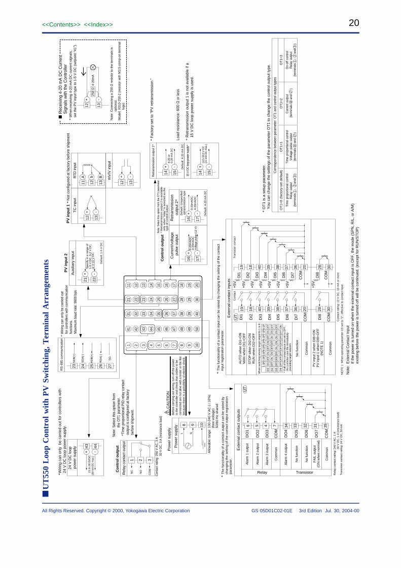
20
All Rights Reserved. Copyright © 2000, Yokogawa Electric Corporation
<<Contents>> <<Index>>
GS 05D01C02-01E 3rd Edition Jul. 30, 2004-00
U
T55
0 L
oop
Con
trol
wit
h P
V S
wit
chin
g, T
erm
inal
Arr
ange
men
ts
1 2 3 4 5 6 7 8 9 10
41 42 43 44 45 46 47 48 49 50
31 32 33 34 35 36 37 38 39 40
21 22 23 24 25 26 27 28 29 30
11 12 13 14 15 16 17 18 19 20
8 9
Pow
er s
uppl
y 10
L N
Allo
wab
le r
ange
: 100
-240
V A
C (
10
%)
(fre
e vo
ltage
) 50
/60
Hz
shar
ed
Pow
er s
uppl
y
12 13
TC
inpu
t
11 12
RTD
inpu
t
13 12 13
mV
/V in
put
21 22
Aux
iliar
y in
put
Spe
cify
in a
ran
ge o
f 1-
5 V
DC
, 0-2
V D
C,
or 0
-10
V D
C.
23 24
RS
-485
com
mun
icat
ion
* W
iring
can
onl
y be
car
ried
out
fo
r con
trolle
rs w
ith c
omm
unic
atio
n
func
tions
.
Max
imum
bau
d ra
te: 9
600
bps
25 26 27
SD
B(+
)
SD
A(-
)
RD
B(+
)
RD
A(-
)
SG
* T
he fu
nctio
nalit
y of
a c
onta
ct in
put c
an b
e va
ried
by c
hang
ing
the
setti
ng o
f the
con
tact
inpu
t reg
istr
atio
n pa
ram
eter
. *
The
func
tiona
lity
of a
con
tact
out
put c
an b
e va
ried
by
ch
angi
ng th
e se
tting
of t
he c
onta
ct o
utpu
t reg
istr
atio
n
para
met
er.
* F
acto
ry-s
et to
“P
V r
etra
nsm
issi
on.”
* R
etra
nsm
issi
on o
utpu
t 1 is
not
ava
ilabl
e if
a
15 V
DC
loop
pow
er s
uppl
y is
use
d.
24 V
DC
loop
po
wer
sup
ply
*Wiri
ng c
an o
nly
be
carr
ied
out f
or c
ontr
olle
rs w
ith
24
V D
C lo
op p
ower
sup
ply.
1 2
Rel
ay c
onta
ct o
utpu
t
3
Co
ntr
ol o
utp
ut
NC
NO
CO
M
Con
tact
ratin
g: 2
50 V
AC
, 3 A
30
V D
C, 3
A (r
esis
tanc
e lo
ad)
*Ti
me
prop
ortio
nal P
ID re
lay
cont
act
out
put i
s co
nfig
ured
at f
acto
ry b
efor
e sh
ipm
ent.
Not
e: S
elec
t thi
s op
tion
from
the
OT1
par
amet
er.
CA
UT
ION
Bef
ore
carr
ying
out
wiri
ng, t
urn
off t
he p
ower
to
the
cont
rolle
r and
che
ck th
at c
able
s to
be
conn
ecte
d ar
e no
t aliv
e w
ith a
test
er o
r the
like
be
caus
e th
ere
is a
pos
sibi
lity
of e
lect
ric s
hock
.
A b B
-+
-+
-+
21.6
-28.
0VD
C(3
0 m
A D
C m
ax.)
43 44
+ -
Def
ault:
1-5
V D
C
OT
1=0
(fac
tory
-set
def
ault)
OT
1=1
Cor
resp
onde
nce
betw
een
para
met
er O
T1 a
nd c
ontro
l out
put t
ypes
OT
1=2
OT
1=3
* O
T1
is a
set
up p
aram
eter
.
You
can
cha
nge
the
setti
ngs
of th
e pa
ram
eter
OT
1 to
cha
nge
the
cont
rol o
utpu
t typ
e.
Tim
e pr
opor
tiona
l con
trol
Rel
ay o
utpu
t (te
rmin
als
,
and
)
12
3
Tim
e pr
opor
tiona
l con
trol
Vol
tage
pul
se o
utpu
t (te
rmin
als
a
nd
)
1617
Cur
rent
out
put
(ter
min
als
and
)16
17O
n-of
f con
trol
Rel
ay o
utpu
t (te
rmin
als
,
and
)
12
3
PV
inp
ut
1P
V in
pu
t 2
* N
ot c
onfig
ured
at f
acto
ry b
efor
e sh
ipm
ent
19 18
Ext
erna
l con
tact
inpu
ts
40 39 38 37 20 28 30
DI1
DI2
DI3
DI4
DI5
DI6
CO
M
CO
M
DI8
AU
TO
whe
n D
I1=
ON
MA
N w
hen
DI1
=O
FF
ST
OP
whe
n D
I2=
ON
R
UN
whe
n D
I2=
OF
F
DI3
DI4
1.SP
2.SP
3.SP
4.SP
ON
ON
OFF
OFF
ON
ON
OFF
OFF
5.SP
6.SP
7.SP
8.SP
ON
ON
OFF
OFF
ON
ON
OFF
OFF
DI5
DI6
OFF
OFF
OFF
OFF
OFF
OFF
ON
OFF
ON
OFF
ON
OFF
ON
OFF
OFF ON
Com
mon
PV
inpu
t 2 w
hen
DI8
=O
N P
V in
put 1
whe
n D
I8=
OF
F(N
OT
E 1
)
Com
mon
Whe
n sw
itchi
ng a
mon
g ta
rget
set
poin
ts 1
to 8
:
19 18 40 39 38 37 20 28 30
DI1
DI2
DI3
DI4
DI5
DI6
CO
M
CO
M
DI8
+5V
+5V
+5V
+5V
+5V
+5V
36D
I736
DI7
+5V
+5V
Con
tact
T
rans
isto
r co
ntac
t
Con
tact
rat
ing:
12
V D
C, 1
0 m
A o
r m
ore
NO
TE
1: W
hen
oper
atin
g pa
ram
ter
U3
set t
o "2
", e
ffect
ive
to c
onta
ct in
put.
No
func
tion
16 17
Cur
rent
/vol
tage
pu
lse
outp
ut
0-20
mA
DC
,4-
20m
AD
CV
olta
ge p
ulse
(12
V)
Co
ntr
ol o
utp
ut
14 15
Ret
rans
mis
sion
out
put 1
*
4-20
or
0-20
mA
DC
14 1515 V
DC
loop
pow
er s
uppl
y*
14.5
-18.
0 V
DC
(21
mA
DC
max
.)
* R
etra
nsm
issi
on o
utpu
t 2 is
ava
ilabl
e
only
whe
n “r
elay
” is
sel
ecte
d as
the
ty
pe o
f con
trol
out
put.
16 17Ret
rans
mis
sion
ou
tput
2*
Def
ault:
4-2
0 m
A D
C
Def
ault:
4-2
0 m
A D
C
0-20
mA
DC
,4-
20m
AD
C
UT
* If
all o
f the
con
tact
inpu
ts a
re s
et to
OFF
,
the
cont
rolle
r use
s th
e im
med
iate
ly
pr
eced
ing
targ
et s
etpo
int.
-+
-+
-+ -+
6 5
Ext
erna
l con
tact
out
puts
4 7 34 33
DO
1
DO
2
DO
3
CO
M
DO
4
DO
5
Relay Transistor
No
func
tion
Ala
rm 1
out
put
Ala
rm 2
out
put
Ala
rm 3
out
put
Com
mon
Ala
rm 4
out
put
32D
O6
31D
O7
35C
OM
No
func
tion
Com
mon
UT
FA
IL o
utpu
t(O
N w
hen
norm
al)
Rel
ay c
onta
ct r
atin
g: 2
40 V
AC
, 1 A
30 V
DC
, 1 A
(re
sist
ance
load
) T
rans
isto
r co
ntac
t rat
ing:
24
V D
C, 5
0 m
A
Load
res
ista
nce:
600
Ω o
r le
ss
12 13
Not
e: C
onne
ctin
g a
250
Ω r
esis
tor
to th
e te
rmin
als
is
o
ptio
nal.
Mod
el: X
010-
250-
2 (r
esis
tor
with
M3.
5 cr
imp-
on te
rmin
al
lugs
)
* W
hen
rece
ivin
g 4-
20 m
A D
C c
urre
nt s
igna
ls,
se
t the
PV
inpu
t typ
e to
1-5
V D
C (
setp
oint
“41
”).
R
ecei
ving
4-2
0 m
A D
C C
urre
nt
S
igna
ls w
ith th
e C
ontr
olle
r
250
Ω4-
20m
A
-+
Def
ault:
Uns
peci
fied
retr
ansm
issi
on ty
pe
Not
e: S
elec
t thi
s op
tion
from
the
OT1
par
amet
er.
Not
e: E
xter
nal C
onta
ct In
put
If
the
pow
er is
turn
ed o
n w
hen
the
exte
rnal
con
tact
inpu
t is
OF
F, t
he m
ode
(SP
N, R
/L, o
r A
/M)
ex
istin
g be
fore
the
pow
er is
turn
ed o
ff w
ill b
e co
ntin
ued.
(ex
cept
for
RU
N/S
TO
P)
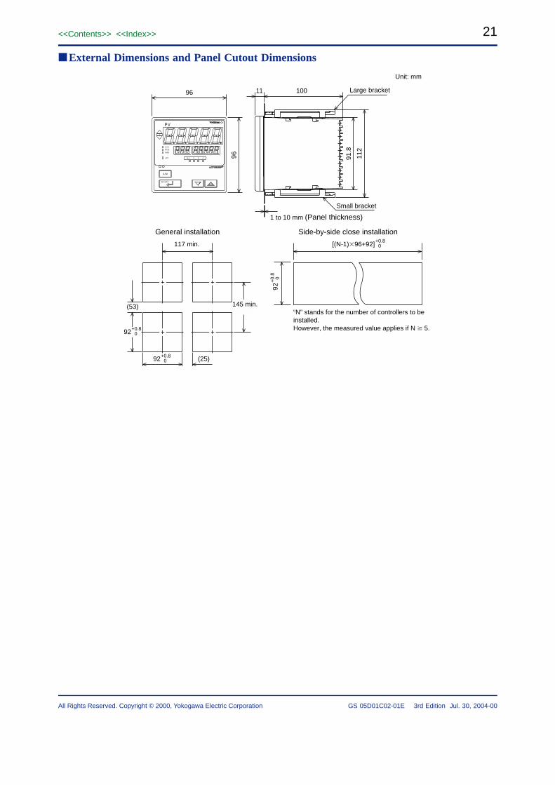
21<<Contents>> <<Index>>
All Rights Reserved. Copyright © 2000, Yokogawa Electric Corporation GS 05D01C02-01E 3rd Edition Jul. 30, 2004-00
External Dimensions and Panel Cutout Dimensions
PV
AL1 2 3 4
CAS
SET/ENT
A /M
REMMAN
LP2
(25)
(53)
[(N-1)96+92]117 min.
145 min.
+0.80
+0.
80
92
+0.8092
+0.8092
“N” stands for the number of controllers to be installed. However, the measured value applies if N 5.
10011
General installation Side-by-side close installation
1 to 10 mm (Panel thickness)
Small bracket
Large bracket
91.8
112
Unit: mm
96
96
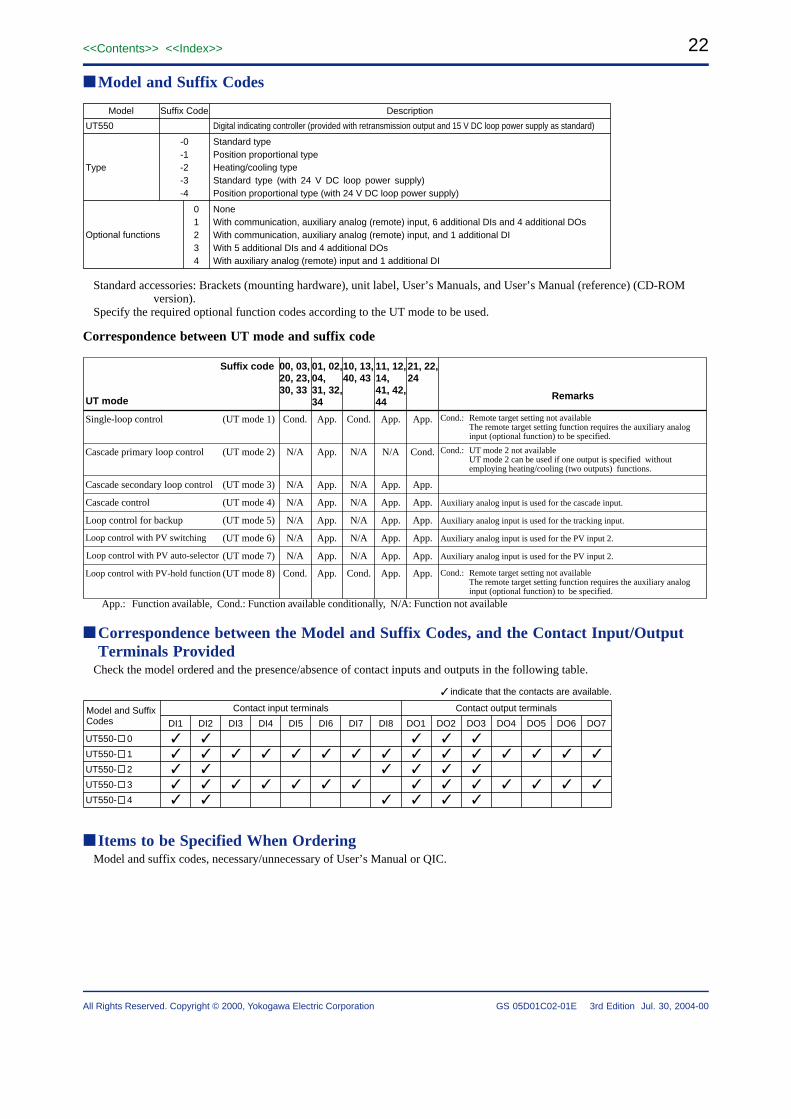
22
All Rights Reserved. Copyright © 2000, Yokogawa Electric Corporation
<<Contents>> <<Index>>
GS 05D01C02-01E 3rd Edition Jul. 30, 2004-00
Model and Suffix Codes
Model Suffix Code Description
UT550 Digital indicating controller (provided with retransmission output and 15 V DC loop power supply as standard)
-0 Standard type-1 Position proportional type-2 Heating/cooling type-3 Standard type (with 24 V DC loop power supply)
Type
-4 Position proportional type (with 24 V DC loop power supply)
0123
Optional functions
4
None With communication, auxiliary analog (remote) input, 6 additional DIs and 4 additional DOs With communication, auxiliary analog (remote) input, and 1 additional DI With 5 additional DIs and 4 additional DOs With auxiliary analog (remote) input and 1 additional DI
Standard accessories: Brackets (mounting hardware), unit label, User’s Manuals, and User’s Manual (reference) (CD-ROMversion).
Specify the required optional function codes according to the UT mode to be used.
Correspondence between UT mode and suffix code
UT mode
Suffix code 00, 03, 20, 23,30, 33
01, 02, 04,31, 32,34
10, 13,40, 43
11, 12, 14,41, 42,44
21, 22, 24
Remarks
Single-loop control
Cascade primary loop control
Cascade secondary loop control
Cascade control
Loop control for backup
Loop control with PV switching
Loop control with PV-hold function
Loop control with PV auto-selector
(UT mode 1)
(UT mode 2)
(UT mode 3)
(UT mode 4)
(UT mode 5)
(UT mode 6)
(UT mode 7)
(UT mode 8)
Cond.
N/A
N/A
N/A
N/A
N/A
Cond.
N/A
App. Cond.
App. N/A
App. N/A
App. N/A
App. N/A
App. N/A
App. Cond.
App. N/A
App.
App.
App.
App.
App.
App.
App.
N/A
App.
Cond.
App.
App.
App.
App.
App.
App.
Cond.: Remote target setting not available The remote target setting function requires the auxiliary analog input (optional function) to be specified.
Cond.: Remote target setting not available The remote target setting function requires the auxiliary analog input (optional function) to be specified.
Auxiliary analog input is used for the cascade input.
Cond.: UT mode 2 not available UT mode 2 can be used if one output is specified without employing heating/cooling (two outputs) functions.
Auxiliary analog input is used for the tracking input.
Auxiliary analog input is used for the PV input 2.
Auxiliary analog input is used for the PV input 2.
App.: Function available, Cond.: Function available conditionally, N/A: Function not available
Correspondence between the Model and Suffix Codes, and the Contact Input/OutputTerminals Provided
Check the model ordered and the presence/absence of contact inputs and outputs in the following table.
Contact input terminals Contact output terminals
indicate that the contacts are available.
Model and Suffix Codes DI1 DI2 DI3 DI4 DI5 DI6 DI7 DO1 DO2 DO3 DO4
UT550- 1
UT550- 0
UT550- 2
UT550- 3
UT550- 4
DI8 DO5 DO6 DO7
Items to be Specified When OrderingModel and suffix codes, necessary/unnecessary of User’s Manual or QIC.