Embed Size (px)
Citation preview
MIC5363/4 High-PSRR, 300mA, µCap LDO in 1.2mm × 1.2mm Thin MLF®
MLF and MicroLead Frame are registered trademarks of Amkor Technology, Inc.
Micrel Inc. • 2180 Fortune Drive • San Jose, CA 95131 • USA • tel +1 (408) 944-0800 • fax + 1 (408) 474-1000 • http://www.micrel.com
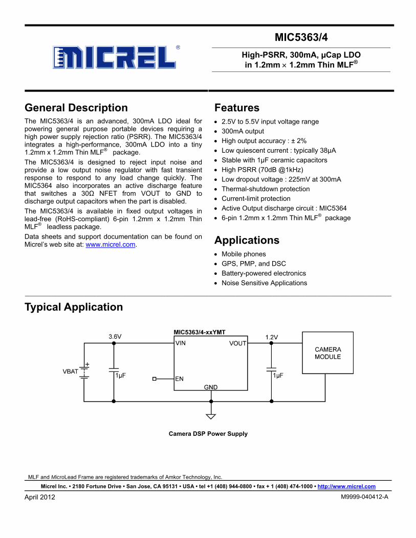
General Description The MIC5363/4 is an advanced, 300mA LDO ideal for powering general purpose portable devices requiring a high power supply rejection ratio (PSRR). The MIC5363/4 integrates a high-performance, 300mA LDO into a tiny 1.2mm x 1.2mm Thin MLF® package. The MIC5363/4 is designed to reject input noise and provide a low output noise regulator with fast transient response to respond to any load change quickly. The MIC5364 also incorporates an active discharge feature that switches a 30Ω NFET from VOUT to GND to discharge output capacitors when the part is disabled. The MIC5363/4 is available in fixed output voltages in lead-free (RoHS-compliant) 6-pin 1.2mm x 1.2mm Thin MLF® leadless package. Data sheets and support documentation can be found on Micrel’s web site at: www.micrel.com.
Features • 2.5V to 5.5V input voltage range • 300mA output • High output accuracy : ± 2% • Low quiescent current : typically 38µA • Stable with 1µF ceramic capacitors • High PSRR (70dB @1kHz) • Low dropout voltage : 225mV at 300mA • Thermal-shutdown protection • Current-limit protection • Active Output discharge circuit : MIC5364 • 6-pin 1.2mm x 1.2mm Thin MLF® package
Applications • Mobile phones • GPS, PMP, and DSC • Battery-powered electronics • Noise Sensitive Applications
_________________________________________________________________________________________________________________________
Typical Application
Camera DSP Power Supply
April 2012
M9999-040412-A
Micrel, Inc. MIC5363/4
April 2012 2 M9999-043012-A
Ordering Information Part Number Marking
Code Voltage(1) Junction Temperature Range Package(2) Lead Finish(3)
MIC5363-1.2YMT 34 1.2 –40°C to +125°C 6-Pin 1.2 mm × 1.2mm Thin MLF® Pb-Free
MIC5363-2.8YMT 3G 2.8 –40°C to +125°C 6-Pin 1.2 mm × 1.2mm Thin MLF® Pb-Free
MIC5363-3.3YMT 3S 3.3 –40°C to +125°C 6-Pin 1.2 mm × 1.2mm Thin MLF® Pb-Free
MIC5364-1.2YMT(4) 44 1.2 –40°C to +125°C 6-Pin 1.2 mm × 1.2mm Thin MLF® Pb-Free
MIC5364-2.8YMT(4) 4X 2.8 –40°C to +125°C 6-Pin 1.2 mm × 1.2mm Thin MLF® Pb-Free
MIC5364-3.3YMT(4) 4S 3.3 –40°C to +125°C 6-Pin 1.2 mm × 1.2mm Thin MLF® Pb-Free
Notes: 1. Other voltages available. Contact Micrel for details.
2. “” = Pin 1 identifier. 3. Green, RoHS-compliant. Level finish is NiPdAu. Mold compound is Halogen free. 4. MIC5364 offers Auto-Discharge function.
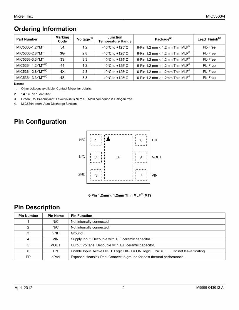
Pin Configuration
6-Pin 1.2mm × 1.2mm Thin MLF® (MT)
Pin Description Pin Number Pin Name Pin Function
1 N/C Not internally connected. 2 N/C Not internally connected. 3 GND Ground.
4 VIN Supply Input. Decouple with 1µF ceramic capacitor.
5 VOUT Output Voltage. Decouple with 1µF ceramic capacitor.
6 EN Enable Input. Active HIGH. Logic HIGH = ON, logic LOW = OFF. Do not leave floating. EP ePad Exposed Heatsink Pad. Connect to ground for best thermal performance.
Micrel, Inc. MIC5363/4
April 2012 3 M9999-043012-A
Absolute Maximum Ratings(1) Supply Voltage (VIN) ........................................ −0.3V to +6V Enable Voltage (VEN)...............................−0.3V to VIN +0.3V Power Dissipation (PD) ........................... Internally Limited(3) Lead Temperature (soldering, 10s)............................ 260°C Junction Temperature (TJ) ........................–40°C to +125°C Storage Temperature (TS).........................–65°C to +150°C ESD Rating(4).................................................................. 2kV
Operating Ratings(2) Supply Voltage (VIN)..................................... +2.5V to +5.5V Enable Voltage (VEN).............................................. 0V to VIN Junction Temperature (TJ) ........................–40°C to +125°C Junction Thermal Resistance 1.2mm × 1.2mm Thin MLF® (θJA).....................173°C/W
Electrical Characteristics(5) VIN = VEN = VOUT + 1V, 2.5V if VOUT ≤ 1.5V; IOUT = 100µA; COUT = 1µF; TJ = 25°C, bold values indicate –40°C to +125°C, unless noted.
Parameter Condition Min. Typ. Max. Units
Variation from nominal VOUT −2.0 2.0 Output Voltage Accuracy
Variation from nominal VOUT, –40°C to +125°C −3.0 3.0 %
Line Regulation(6) VIN = Max(VOUT + 1V, 2.5V) to 5.5V, IOUT =100µA 0.02 0.2 %/V
Load Regulation IOUT =100µA to 300mA 0.3 0.7 %
IOUT =50mA; VOUT ≥ 2.8V 35 65
IOUT =300mA; VOUT ≥ 2.8V 225 380
IOUT =50mA; 2.5V ≤ VOUT < 2.8V 55 100 Dropout Voltage
IOUT =300mA; 2.5V ≤ VOUT < 2.8V 300 600
mV
VEN = High; IOUT = 0mA 38 53 Ground Pin Current
VEN = High; IOUT = 300mA 55 70 µA
Shutdown Current VEN = 0V 0.1 1 µA
Supply Ripple Rejection f = 1kHz; COUT = 1µF 70 dB
Current Limit VOUT = 0V 325 520 680 mA
Output Voltage Noise COUT = 1µF; 10Hz to 100kHz 200 µVRMS
Auto-Discharge NFET Resistance MIC5364 only; VEN = 0V; VIN = 3.6V; IOUT = −3mA 30 Ω
Enable Inputs (EN)
Logic Low 0.2 Enable Input Voltage
Logic High 1.2 V
VIL ≤ 0.2V 0.01 1 Enable Input Current
VIH ≥ 1.2V 0.01 1 µA
Turn-On Time COUT = 1µF 60 150 µs
Notes: 1. Exceeding the absolute maximum rating may damage the device. 2. The device is not guaranteed to function outside its operating rating. 3. The maximum allowable power dissipation of any TA (ambient temperature) is PD(max) =(TJ(max) – TA) / θJA. Exceeding the maximum allowable power
dissipation will result in excessive die temperature, and the regulator will go into thermal shutdown. 4. Devices are ESD sensitive. Handling precautions recommended. Human body model, 1.5kΩ in series with 100pF. 5. Specification for packaged product only. 6. Regulation is measured at constant junction temperature using low duty cycle pulse testing; changes in output voltage due to heating effects are
covered by the thermal regulation specification. 7. Dropout voltage is defined as the input-to-output differential at which the output voltage drops 2% below its nominal value.
Micrel, Inc. MIC5363/4
April 2012 4 M9999-043012-A
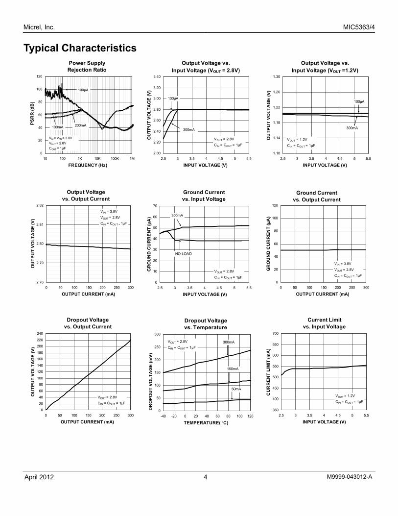
Typical Characteristics
Output Voltagevs. Output Current
2.78
2.79
2.80
2.81
2.82
0 50 100 150 200 250 300
OUTPUT CURRENT (mA)
OU
TPU
T VO
LTA
GE
(V)
VIN = 3.8VVOUT = 2.8VCIN = COUT = 1µF
Ground Current
vs. Output Current
20
40
60
80
100
120
00 50 100 150 200 250 300
GR
OU
ND
CU
RR
ENT
(µA
)
OUTPUT CURRENT (mA)
VIN = 3.8VVOUT = 2.8VCIN = COUT = 1µF
Dropout Voltagevs. Output Current
20
40
60
80
100
120
140
160
180
200
220
240
OU
TPU
T VO
LTA
GE
(V)
00 50 100 150 200 250 300
OUTPUT CURRENT (mA)
VOUT = 2.8VCIN = COUT = 1µF
Current Limit vs. Input Voltage
400
450
500
550
600
650
700
CU
RR
ENT
LIM
IT (m
A)
3502.5 3 3.5 4 4.5 5 5.5
INPUT VOLTAGE (V)
VOUT = 1.2VCIN = COUT = 1µF
Power Supply Rejection Ratio
0
20
40
60
80
100
120
10 100 1K 10K 100K 1M
FREQUENCY (Hz)
PSR
R (d
B)
VIN = VEN = 3.8VVOUT = 2.8VCOUT = 1µF
100µA
200mA100mA
Output Voltage vs. Input Voltage (VOUT = 2.8V)
2.00
2.20
2.40
2.60
2.80
3.00
3.20
3.40
2.5 3 3.5 4 4.5 5 5.5
INPUT VOLTAGE (V)
OU
TPU
T VO
LTA
GE
(V)
100µA
300mA
VOUT = 2.8VCIN = COUT = 1µF
Output Voltage vs. Input Voltage (VOUT =1.2V)
1.10
1.14
1.18
1.22
1.26
1.30
2.5 3 3.5 4 4.5 5 5.5
INPUT VOLTAGE (V)
OU
TPU
T VO
LTA
GE
(V)
100µA
300mA
VOUT = 1.2VCIN = COUT = 1µF
Ground Current vs. Input Voltage
0
10
20
30
40
50
60
70
2.5 3 3.5 4 4.5 5 5.5
INPUT VOLTAGE (V)
GR
OU
ND
CU
RR
ENT
(µA
) 300mA
NO LOAD
VOUT = 2.8VCIN = COUT = 1µF
Dropout Voltage vs. Temperature
0
50
100
150
200
250
300
-40 -20 0 20 40 60 80 100 120
TEMPERATURE( °C)
DR
OPO
UT
VOLT
AG
E (m
V)
300mA
150mA
50mA
VOUT = 2.8VCIN = COUT = 1µF
Micrel, Inc. MIC5363/4
April 2012 5 M9999-043012-A
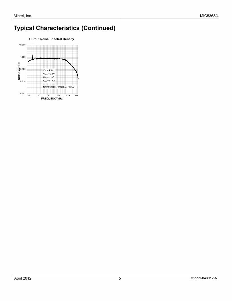
Typical Characteristics (Continued) Output Noise Spectral Density
0.010
0.100
1.000
10.000
NO
ISE
uV/√
Hz
0.001
FREQUENCY (Hz)
VIN = 4.5VVOUT = 2.8VCOUT = 1µFIOUT = 51mA
NOISE (10Hz - 100kHz) = 192µV
10 100 1K 10K 100K 1M
Micrel, Inc. MIC5363/4
April 2012 6 M9999-043012-A
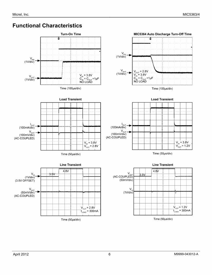
Functional Characteristics
Micrel, Inc. MIC5363/4
April 2012 7 M9999-043012-A
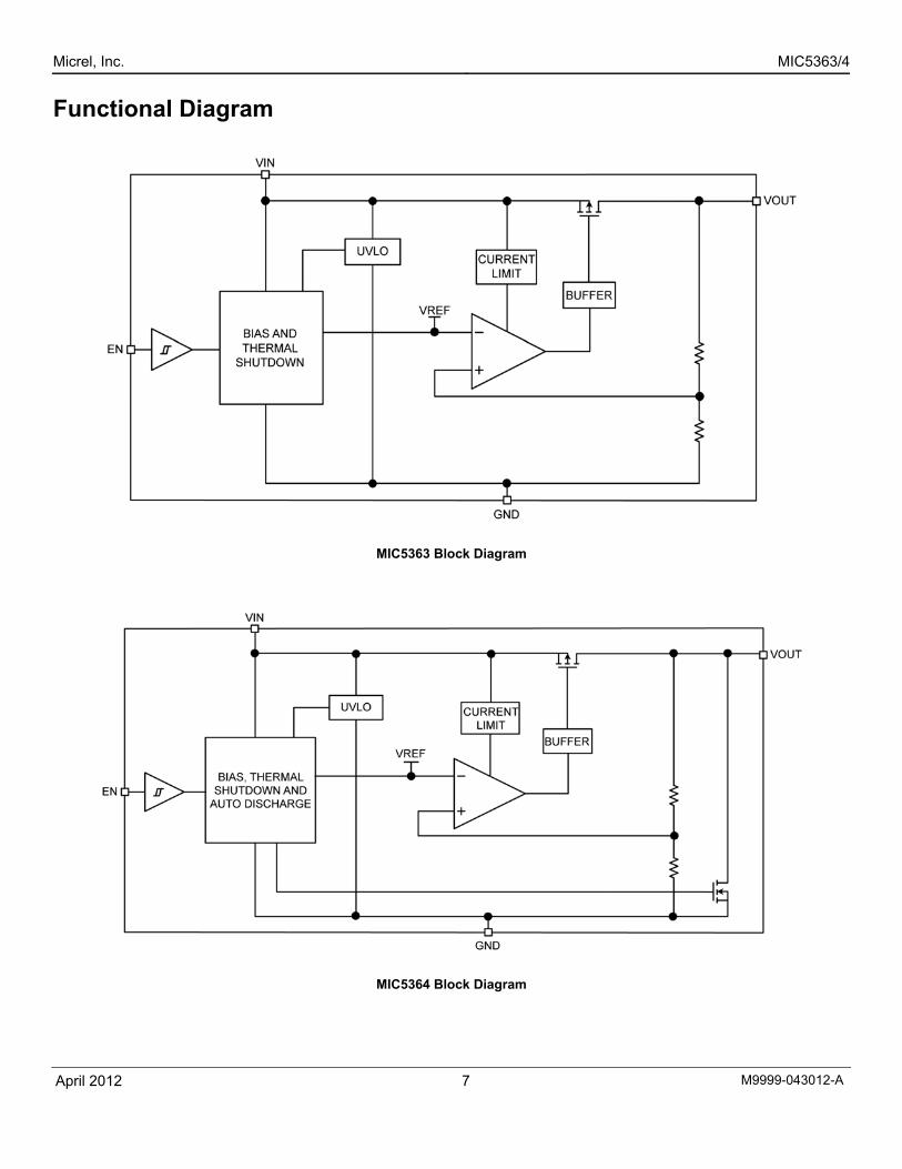
Functional Diagram
MIC5363 Block Diagram
MIC5364 Block Diagram
Micrel, Inc. MIC5363/4
April 2012 8 M9999-043012-A
Application Information The MIC5363/4 is a 300mA LDO, packaged in a 1.2mm x 1.2mm Thin MLF® package. The MIC5364 includes an auto-discharge feature which automatically discharges the output capacitor when the output is disabled. The MIC5363/4 consists of an internal reference, error amplifier, P-channel pass transistor, and internal feedback resistors. The error amplifier compares the feedback voltage with that of the reference. Depending upon whether the feedback is lower or higher than the reference determines whether the gate of the pass transistor is pulled low to allow more current and increase output voltage or pulled high to reduce current. The MIC5363/4 regulator is fully protected from damage due to fault conditions through linear current limiting and thermal shutdown.
Input Capacitor The MIC5363/4 is a high-performance, high-bandwidth device. An input capacitor of 1µF from the input pin to ground is required to provide stability. Low-ESR ceramic capacitors provide optimal performance in small board area. Additional high-frequency capacitors, such as small valued NPO dielectric type capacitors, help filter out high-frequency noise and are good practice in any RF-based circuit. X5R or X7R dielectrics are recommended for the input capacitor. Y5V dielectrics lose most of their capacitance over temperature and are therefore not recommended.
Output Capacitor The MIC5363/4 requires an output capacitor of 1µF or greater to maintain stability. The design is optimized for use with low-ESR ceramic chip capacitors. High-ESR capacitors may cause high-frequency oscillation. The output capacitor can be increased, but performance has been optimized for a 1µF ceramic output capacitor. X7R and X5R dielectric ceramic capacitors are recommended for their temperature performance. X7R capacitors change capacitance by 15% over their operating temperature range and are the most stable type of ceramic capacitors. Z5U and Y5V dielectric capacitors change value by as much as 50% and 60% respectively over their operating temperature ranges. To use a ceramic-chip capacitor with Y5V dielectric the value must be much higher than an X7R ceramic capacitor to ensure the same minimum capacitance over the equivalent operating temperature range.
No Load Stability The MIC5363/4 will remain stable and in regulation without the need of a minimum load. This reduces the amount and therefore cost of external components.
Enable/Shutdown The MIC5363/4 comes with an active-high enable pin that allows the regulator to be disabled. Forcing the enable pin low disables the regulator and sends it into an off-mode current state drawing virtually zero current. When disabled, the MIC5364 switches an internal 30Ω load on the regulator output to discharge the external capacitor. Forcing the enable pin high enables the output voltage. The active-high enable pin uses CMOS technology and cannot be left floating. A floating enable pin may cause an indeterminate state on the output.
Thermal Considerations The MIC5363/4 is designed to provide a 300mA continuous current output in a very-small package. Maximum operating temperature can be calculated based on the output currents and the voltage drop across the part. For example, if the input voltage is 3.6V, VOUT = 2.8V and the output current = 300mA. The actual power dissipation of the regulator circuit can be determined using the equation:
PD = (VIN − VOUT) IOUT + VIN IGND Because this is a CMOS device and the ground current is typically <60µA over the load range, the power dissipation contributed by the ground current is < 1% which can be ignored for this calculation:
PD = (3.6V − 2.8V) × 300mA PD = 0.24W
To determine the maximum ambient operating temperature of the package, use the junction to ambient thermal resistance of the device and the following basic equation:
⎟⎟
⎠
⎞
⎜⎜
⎝
⎛=
JA
AJ(MAX)D(MAX) θ
T - T P
TJ(MAX) = 125°C θJA = 173°C/W
Micrel, Inc. MIC5363/4
April 2012 9 M9999-043012-A
Substituting PD for PD(MAX) and solving for the ambient operating temperature will give the maximum operating conditions for the regulator circuit. The junction-to- ambient thermal resistance for the standard footprint is 173°C/W. The maximum power dissipation must not be exceeded for proper operation. For example, when operating a 2.8V application with an input voltage of 3.6V and 300mA output with a standard footprint layout, the maximum ambient operating temperature TA can be determined as follows:
0.24W = (125°C − TA) / (173°C/W) TA = 83°C
Therefore, a MIC5363-2.8YMT application with a 300mA output current can accept an ambient operating temperature of 83°C in a 1.2mm x 1.2mm Thin MLF® package. For a full discussion of heat sinking and thermal effects on voltage regulators refer to the “Regulator Thermals” section of Micrel’s Designing with Low-Dropout Voltage Regulators handbook. This information can be found on Micrel's website at: http://www.micrel.com/_PDF/other/LDOBk_ds.pdf
Micrel, Inc. MIC5363/4
April 2012 10 M9999-043012-A
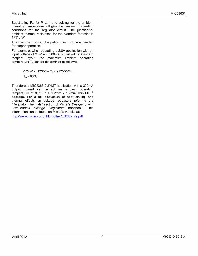
Evaluation Board Schematic
Bill of Materials Item Part Number Manufacturer Description Qty. C1, C2 GRM155R61A105KE15D Murata(1) 1µF/6.3V ceramic capacitor, X5R, size 0402 2 R1 CRCW04021003FKED Vishay(2) Resistor, 100k (0403 size), 1% 1 U1 MIC5363/4-xxYMT Micrel, Inc.(3) 300mA µCap LDO in 1.2mm × 1.2mm Thin MLF® 1
Notes: 1. Murata Tel: www.murata.com. 2. Vishay: www.vishay.com. 3. Micrel, Inc.: www.micrel.com.
Micrel, Inc. MIC5363/4
April 2012 11 M9999-043012-A
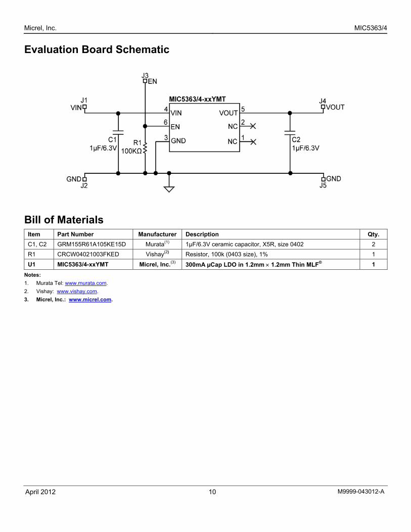
PCB Layout Recommendations
Top Layer
Bottom Layer
Micrel, Inc. MIC5363/4
April 2012 12 M9999-043012-A
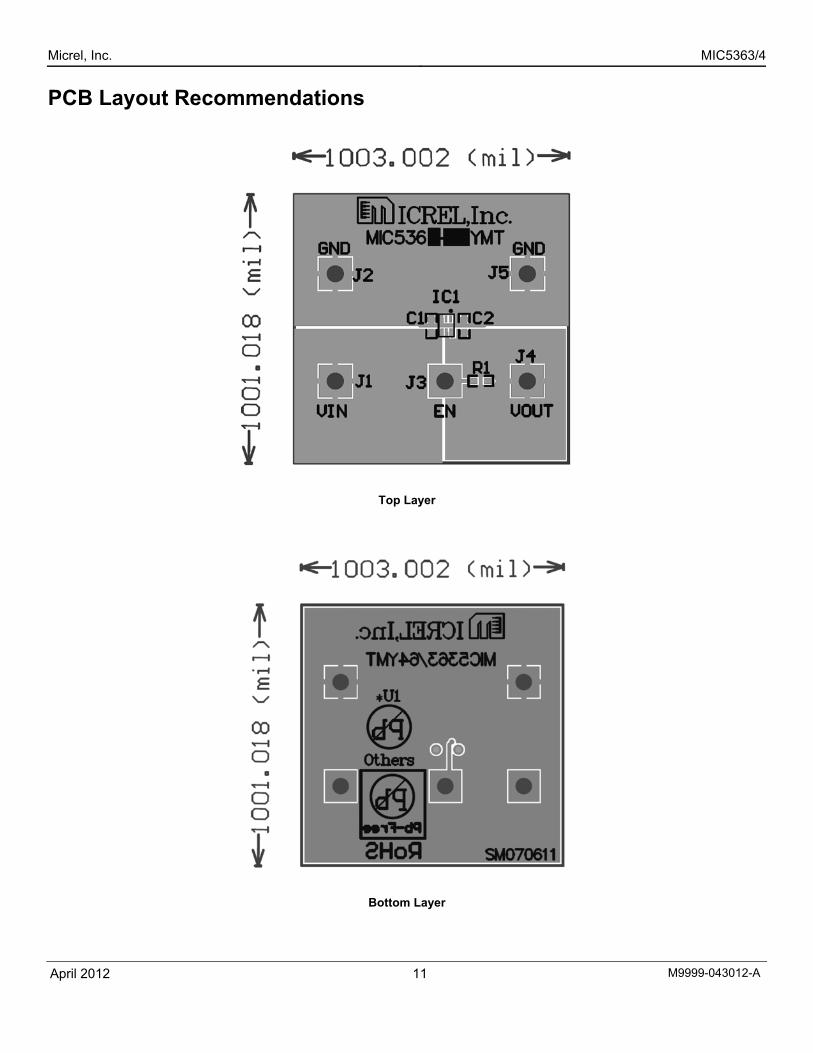
Package Information
6-Pin 1.2mm × 1.2mm Thin MLF®
MICREL, INC. 2180 FORTUNE DRIVE SAN JOSE, CA 95131 USA TEL +1 (408) 944-0800 FAX +1 (408) 474-1000 WEB http://www.micrel.com
Micrel makes no representations or warranties with respect to the accuracy or completeness of the information furnished in this data sheet. This
information is not intended as a warranty and Micrel does not assume responsibility for its use. Micrel reserves the right to change circuitry, specifications and descriptions at any time without notice. No license, whether express, implied, arising by estoppel or otherwise, to any intellectual
property rights is granted by this document. Except as provided in Micrel’s terms and conditions of sale for such products, Micrel assumes no liability whatsoever, and Micrel disclaims any express or implied warranty relating to the sale and/or use of Micrel products including liability or warranties
relating to fitness for a particular purpose, merchantability, or infringement of any patent, copyright or other intellectual property right.
Micrel Products are not designed or authorized for use as components in life support appliances, devices or systems where malfunction of a product can reasonably be expected to result in personal injury. Life support devices or systems are devices or systems that (a) are intended for surgical
implant into the body or (b) support or sustain life, and whose failure to perform can be reasonably expected to result in a significant injury to the user. A Purchaser’s use or sale of Micrel Products for use in life support appliances, devices or systems is a Purchaser’s own risk and Purchaser agrees to
fully indemnify Micrel for any damages resulting from such use or sale.
© 2012 Micrel, Incorporated.