Embed Size (px)
Citation preview

IN-GATE-2015 PAPER| www.gateforum.com
© All rights reserved by GATE Forum Educational Services Pvt. Ltd. No part of this booklet may be reproduced or utilized
in any form without the written permission. Discuss this questions paper at www.gatementor.com.
1
General Aptitude
Q. No. 1 – 5 Carry One Mark Each
1. Five teams have to compete in a league, with every team playing every other team exactly
once before going to the next round. How many matches will have to be held to complete
the league round of matches?
(A) 20 (B) 10 (C) 8 (D) 5
Answer: (B)
Exp: For a match to be played, we need 2 teams
No. of matches = No. of ways of selections 2 teams out of 5 5
2C 10
2. Fill in the blank with the correct idiom/phrase.
That boy from the town was a _____ in the sleepy village.
(A) dog out of herd (B) sheep from the heap
(C) fish out of water (D) bird from the flock
Answer: (C)
Exp: From the statement, it appears that boy found it tough to adapt to a very different
situation.
3. Choose the statement where underlined word is used correctly.
(A) When the teacher eludes to different authors, he is being elusive.
(B) When the thief keeps eluding the police, he is being elusive.
(C) Matters that are difficult to understand, indentify or remember are allusive.
(D) Mirages can be allusive, but a better way to express them is illusory.
Ans: (B)
Exp: Elusive: Difficult to answer.
4. Tanya is older than Eric. Cliff is older than Tanya. Eric is older than Cliff.
If the first two statements are true, then the third statement is:
(A) True (B) False (C) Uncertain (D) Data insufficient
Ans: (B)
5. Choose the appropriate word/phrase, out of the four options given below, to complete the
following sentence:
Apparent lifelessness ___________ dormant life.
(A) harbours (B) leads to (C) supports (D) affects
Answer: (A)
Exp: Apparent: looks like
dormant: hidden
Harbour: give shelter
Effect (verb): results in

IN-GATE-2015 PAPER| www.gateforum.com
© All rights reserved by GATE Forum Educational Services Pvt. Ltd. No part of this booklet may be reproduced or utilized
in any form without the written permission. Discuss this questions paper at www.gatementor.com.
2
Q. No. 6 – 10 Carry Two Marks Each
6. A coin tossed thrice. Let X be the event that head occurs in each of the first two tosses.
Let Y be the event that a tail occurs on the third toss. Let Z be the event that two tails
occurs in three tosses.
Based on the above information, which one of the following statements is TRUE?
(A) X and Y are not independent (B) Y and Z are dependent
(C) Y and Z are independent (D) X and Z are independent
Answer: (B)
Exp: Let y as tail occurred in third toss
and z as two tails in third toss which can be {TTH, THT, HTT}
y = {TTH, TTT}
∴ both y and z are dependent.
7. Given below are two statements followed by two conclusions. Assuming these statements
to be true, decide which one logically follows.
Statements:
I. No manager is a leader.
II. All leaders are executives.
Conclusions:
I. No manager is an executive.
II. No executive is a manager.
(A) Only conclusion I follows. (B) Only conclusion II follows.
(C) Neither conclusion I nor II follows. (D) Both conclusions I and II follow.
Answer: (C)
Exp:
Therefore concluding diagram can be
It can be manager that is manager can be executive also.
Some executives are also leaders that is not a manager
Executive
L NL

IN-GATE-2015 PAPER| www.gateforum.com
© All rights reserved by GATE Forum Educational Services Pvt. Ltd. No part of this booklet may be reproduced or utilized
in any form without the written permission. Discuss this questions paper at www.gatementor.com.
3
8. In the given figure angle Q is a right angle, PS:QS=3:1, RT:QT=5:2 and PU:UR=1:1. If
area of triangle QTS is 20 cm2, then the area of triangle PQR in cm
2 is ________.
Answer: 280
Exp: Let area of triangle PQR be „A‟
le
SQ 1 1
PQ 1 3 4
QT 2 2
QR 2 5 7
1Area of QTS SQ QT
2
1 1 2
PQ QR2 4 7
1 2 1
PQ QR4 7 2
le1Area of PQR
14
2
2
1given 20cm A
14
A 14 20 280cm
9. Select the appropriate option in place of underlined part of the sentence.
Increased productivity necessary reflects greater efforts made by the employees.
(A) Increase in productivity necessary (B) Increase productivity is necessary
(C) Increase in productivity necessarily (D) No improvement required
Answer: (C)
10. Right triangle PQR is to be constructed in the xy-plane so that the right angle is at P and
line PR is parallel to the x-axis. The x and y coordinates of P, Q, and R are to be integers
that satisfy the inequalities: 4 x 5 and 6 y 16. How many different triangles could
be constructed with these properties?
(A) 110 (B) 1,100 (C) 9,900 (D) 10,000
Answer: (C)
R
TU
P S Q

IN-GATE-2015 PAPER| www.gateforum.com
© All rights reserved by GATE Forum Educational Services Pvt. Ltd. No part of this booklet may be reproduced or utilized
in any form without the written permission. Discuss this questions paper at www.gatementor.com.
4
Exp:
1 1
1 1
2 1 2
2 1 2
X 4 X 5
Y 6 Y 16
X 9 chairs X X
Y 10 chairs Y Y
Total triangles 10 11 9 10 9900
Instrumentation Engineering
Q. No. 1 – 25 Carry One Mark Each
1. The capacitor shown in the figure is initially charged to +10 V. The switch closes at time
t=0. Then the value of cV (t) in volts at time t=10 ms is _____ V.
Answer: 3.67
Exp: It is a source free network where capacitor voltage
3
t
c 0
100t
100 10 103
c
V t V e ; t 0
10e
V 10 10 10e 3.67V
1
RC100
2. The voltage 0(E ) developed across a glass electrode for pH measurement is related to the
temperature (T) by the relation
(A) 0 2
1E
T (B) o
1E
T (C) 0E T (D) 2
0E T
Answer: (C)
3. Let 3+4j be a zero of a fourth order linear –phase FIR filter. The complex number which
is NOT a zero of this filter is
(A) 3 4j (B) 3 4
j25 25
(C) 3 4
j25 25
(D) 1 1
j3 4
Answer: (D)
Exp: The property of a FIR filter is that if Zo is a zero then the remaining zeros are
t 0
R 10k C 1 F
cV (t)

IN-GATE-2015 PAPER| www.gateforum.com
© All rights reserved by GATE Forum Educational Services Pvt. Ltd. No part of this booklet may be reproduced or utilized
in any form without the written permission. Discuss this questions paper at www.gatementor.com.
5
0
0 0
1 1, Z *, *
Z Z
3 4 3 4j , 3 4j , j
25 25 25 25
So option (D) is not matching with any of this.
4. The bridge most suited for measurement of a four-terminal resistance in the range of
0.001 to 0.1 is
(A) Wien‟s bridge (B) Kelvin double bridge
(C) Maxwell‟s bridge (D) Schering bridge
Answer: (B)
5. A load resistor RL is connected to a battery of voltage E with internal resistance Ri
through a resistance Rs as shown in the figure. For fixed values of L iR and R , the value
of SR 0 for maximum power transfer to RL is
(A) 0 (B) L iR R (C) LR (D) L iR R
Answer: (A)
Exp: When load is constant, we should see for what value of resistance current will be
maximum and LRP max .
6. A mass-spring-damper system with force as input and displacement of the mass as output
has a transfer function 2G(s) 1/ s 24s 900 . A force input F(t)=10 sin(70t) Newtons
is applied at time t = 0s. A beam from an optical stroboscope is focused on the mass. In
steady state, the strobe frequency in hertz at which the mass appears to be stationary is
(A) 5 / (B) 15 / (C) 35 / (D) 50 /
Answer: (C)
iR
ELR
sR
IN-GATE-2015 PAPER| www.gateforum.com
© All rights reserved by GATE Forum Educational Services Pvt. Ltd. No part of this booklet may be reproduced or utilized
in any form without the written permission. Discuss this questions paper at www.gatementor.com.
6
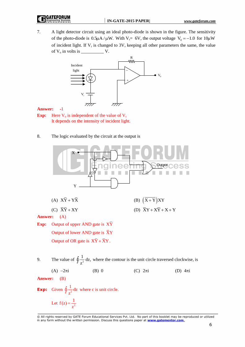
7. A light detector circuit using an ideal photo-diode is shown in the figure. The sensitivity
of the photo-diode is 0.5 A / W. With Vr= 6V, the output voltage 0V 1.0 for 10 W
of incident light. If Vr is changed to 3V, keeping all other parameters the same, the value
of Vo in volts is __________ V.
Answer: -1
Exp: Here Vo is independent of the value of Vr
It depends on the intensity of incident light.
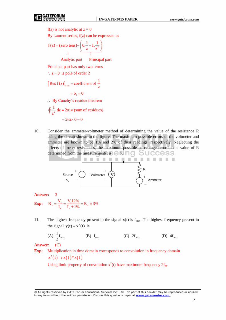
8. The logic evaluated by the circuit at the output is
(A) XY YX (B) X Y XY
(C) XY XY (D) XY XY X Y
Answer: (A)
Exp: Output of upper AND gate is XY
Output of lower AND gate is XY
Output of OR gate is XY XY .
9. The value of 2
1dz,
z where the contour is the unit circle traversed clockwise, is
(A) 2 i (B) 0 (C) 2 i (D) 4 i
Answer: (B)
Exp: Given 2
1dz
z where c is unit circle.
Let 2
1f (z)
z
rV
0V
R
Incident
light
X
Y
Output
IN-GATE-2015 PAPER| www.gateforum.com
© All rights reserved by GATE Forum Educational Services Pvt. Ltd. No part of this booklet may be reproduced or utilized
in any form without the written permission. Discuss this questions paper at www.gatementor.com.
7
f(z) is not analytic at z = 0
By Laurent series, f(z) can be expressed as
2
1 1f (z) (zero tens) 0. 1.
z z
Analytic part Principal part
Principal part has only two terms
z 0 is pole of order 2
z 0
1Res f (z) coefficient of
z
1b 0
By Cauchy‟s residue theorem
2
1dz 2 i (sum of residues)
z
2 i 0 0
10. Consider the ammeter-voltmeter method of determining the value of the resistance R
using the circuit shown in the figure. The maximum possible errors of the voltmeter and
ammeter are known to be 1% and 2% of their readings, respectively. Neglecting the
effects of meter resistances, the maximum possible percentage error in the value of R
determined from the measurements, is ___ %.
Answer: 3
Exp: x xx x
x x
V V I2%R R 3%
I I 1%
11. The highest frequency present in the signal x(t) is fmax. The highest frequency present in
the signal 2y(t) x (t) is
(A) max
1f
2 (B) maxf (C) max2f (D) max4f
Answer: (C)
Exp: Multiplication in time domain corresponds to convolution in frequency domain
2x t x f *x f
Using limit property of convolution x2(t) have maximum frequency 2fm.
i
Source
V
R
Voltmeter
Ammeter
V
IN-GATE-2015 PAPER| www.gateforum.com
© All rights reserved by GATE Forum Educational Services Pvt. Ltd. No part of this booklet may be reproduced or utilized
in any form without the written permission. Discuss this questions paper at www.gatementor.com.
8
12. Let A be an n×n matrix with the rank r 0 r n . Then Ax=0 has p independent
solutions, where p is
(A) r (B) n (C) n-r (D) n+r
Answer: (C)
Exp: Given AX=0
n nA r 0 r n
p = no. of independent solution
i.e nullity = p
We know that rank + nullity = n
r p n
p n r
13. The double integral a y
0 0f (x, y) dxdy is equivalent to
(A) x y
0 0f (x, y) dxdy (B)
a y
0 xf (x, y) dxdy
(C) a a
0 xf (x, y) dxdy (D)
a a
0 0f (x, y) dxdy
Answer: (C)
Exp: Given double integral a y
0 0f (x, y)dx. dy
and x=0 to x=y, y=0 to y=a
the diagram is
By applying change of order of integration
a a
x 0 y xf (x,y)dydx
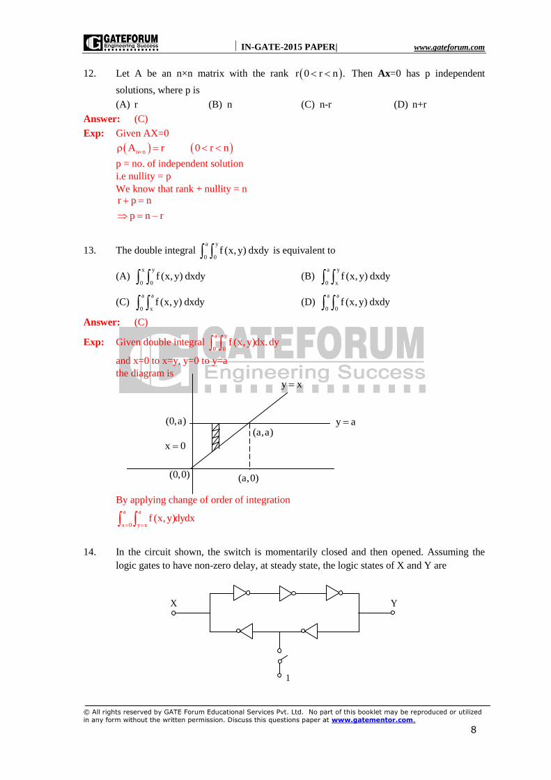
14. In the circuit shown, the switch is momentarily closed and then opened. Assuming the
logic gates to have non-zero delay, at steady state, the logic states of X and Y are
X Y
1
(0,a)
x 0
(0,0) (a,0)
(a,a)
y x
y a

IN-GATE-2015 PAPER| www.gateforum.com
© All rights reserved by GATE Forum Educational Services Pvt. Ltd. No part of this booklet may be reproduced or utilized
in any form without the written permission. Discuss this questions paper at www.gatementor.com.
9
(A) X is latched, Y toggles continuously (B) X and Y are both latched
(C) Y is latched, X toggles continuously (D) X and Y both toggle continuously
Answer: (D)
Exp: The above circuit is a stable multivibrator circuit, where odd numbers of inverter are there
in the loop. In such a circuit, irrespective of the position of output, it always toggles.
Latching means X and Y will be fixed to same value, in this case it is not possible.
15. Consider the logic circuit with input signal TEST shown in the figure. All gates in the
figure shown have identical non-zero delay. The signal TEST which was at logic LOW is
switched to logic HIGH and maintained at logic HIGH. The output
(A) stays HIGH throughout (B) stays LOW throughout
(C) pulses from LOW to HIGH to LOW (D) pulses from HIGH to LOW to HIGH
Answer: (D)
Exp: For analysis point of view, assume delay of each gate is 10 msec. However we can take
any value.
By referring the circuit the upper input to the NAND gate is direct test signal.
The lower input to NAND gate is TEST but with a delay of 30 nsec.
Assuming the delay of NAND gate is 0. First draw output waveform (ideal case) then
shift that by 10 msec. i.e. introduce the delay.
TEST Output
Test
Test
with delay 30nsec
Output with
delay 0
30 nsec0
0
0
Output with
NAND gate
delay 10 n sec40 nsec0 10 nsec

IN-GATE-2015 PAPER| www.gateforum.com
© All rights reserved by GATE Forum Educational Services Pvt. Ltd. No part of this booklet may be reproduced or utilized
in any form without the written permission. Discuss this questions paper at www.gatementor.com.
10
So we can clearly say that initial output change from high to low, then it changes from
low to high and then finally at steady state output is 1.
Note: Saying output is high (option A) will be wrong here. We are not interested to find
steady state output.
16. A p-type semiconductor strain gauge has a nominal resistance of 1000 and a gauge
factor of +200 at o25 C. The resistance of the strain gauge in ohms when subjected to a
strain of 410 m m at the same temperature is _________ .
Answer: 1020
Exp:
1
4R R
GF R 200 10 1000
20
p-type semiconductor have a positive gauge factor
i.e., Resistance with in strain
∴ Rstrained = 1000+20 = 1020
17. A system with transfer function 2
1G s
s 1
has zero initial conditions. The percentage
overshoot in its step response is _________ %.
Answer: 100
Exp: Comparing the denominator, 0
21
% Overshoot e 100 100
18. Liquid flow rate is measured using
(A) a Pirani gauge (B) a pyrometer
(C) an orifice plate (D) a Bourdon tube
Answer: (C)
19. The magnitude of the directional derivative of the function 2 2f x,y x 3y in a
direction normal to the circle 2 2x y 2, at the point (1, 1) , is
(A) 4 2 (B) 5 2 (C) 7 2 (D) 9 2
Answer: (A)
Exp: Let 2 2f (x,y) x 3y
Let 2 2x y 2 and P is (1,1)
Normal to the surface
i j
x y
2xi 2yj
IN-GATE-2015 PAPER| www.gateforum.com
© All rights reserved by GATE Forum Educational Services Pvt. Ltd. No part of this booklet may be reproduced or utilized
in any form without the written permission. Discuss this questions paper at www.gatementor.com.
11
at (1,1)
2i 2j
Le a 2i 2j
We need to calculate magnitude of directional derivatives of f along a at (1,1)
Magnitude of directional deviations ˆf .a
(1,1)
f ff i j 2xi 6yj
x y
f 2i 6j
a 4 4 2 2
2i 2j i ja
2 2 2
Magnitude of direction derivative i j
2i 6j .2
2 6 8
4 22 2
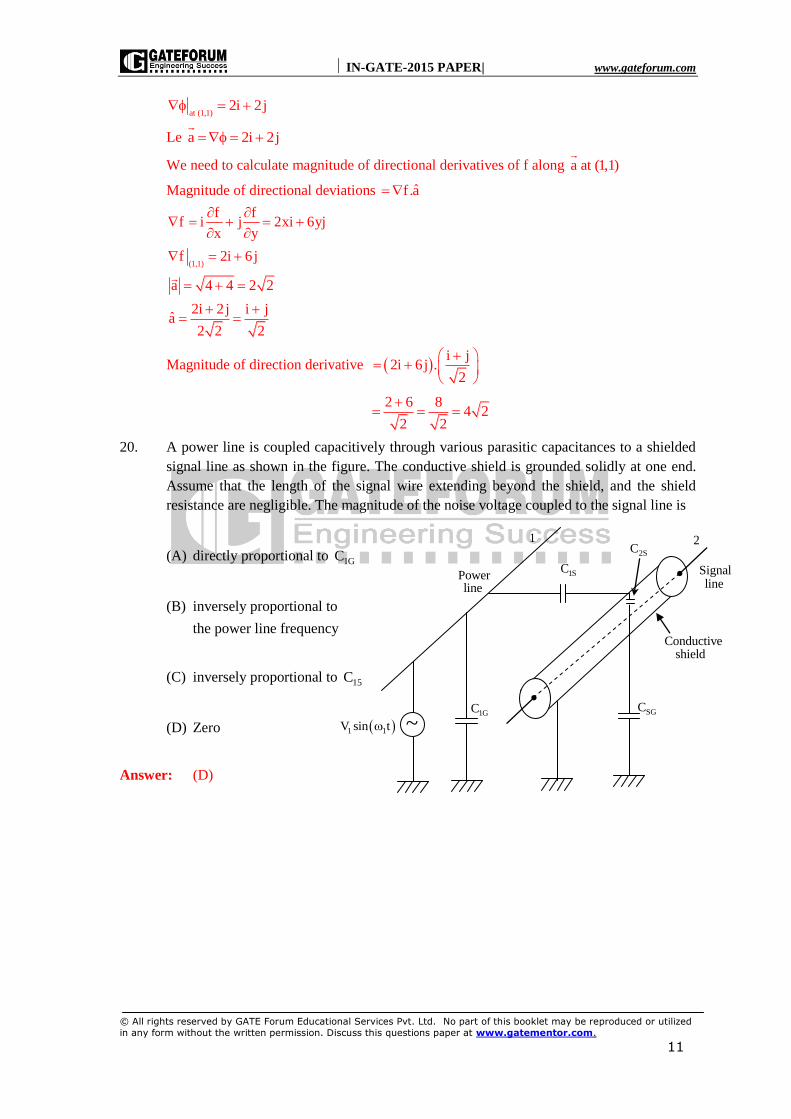
20. A power line is coupled capacitively through various parasitic capacitances to a shielded
signal line as shown in the figure. The conductive shield is grounded solidly at one end.
Assume that the length of the signal wire extending beyond the shield, and the shield
resistance are negligible. The magnitude of the noise voltage coupled to the signal line is
(A) directly proportional to 1GC
(B) inversely proportional to
the power line frequency
(C) inversely proportional to 15C
(D) Zero
Answer: (D)
~ 1 1V sin t1GC
1SC
SGC
2SC2
Signalline
Conductiveshield
Powerline
1
IN-GATE-2015 PAPER| www.gateforum.com
© All rights reserved by GATE Forum Educational Services Pvt. Ltd. No part of this booklet may be reproduced or utilized
in any form without the written permission. Discuss this questions paper at www.gatementor.com.
12
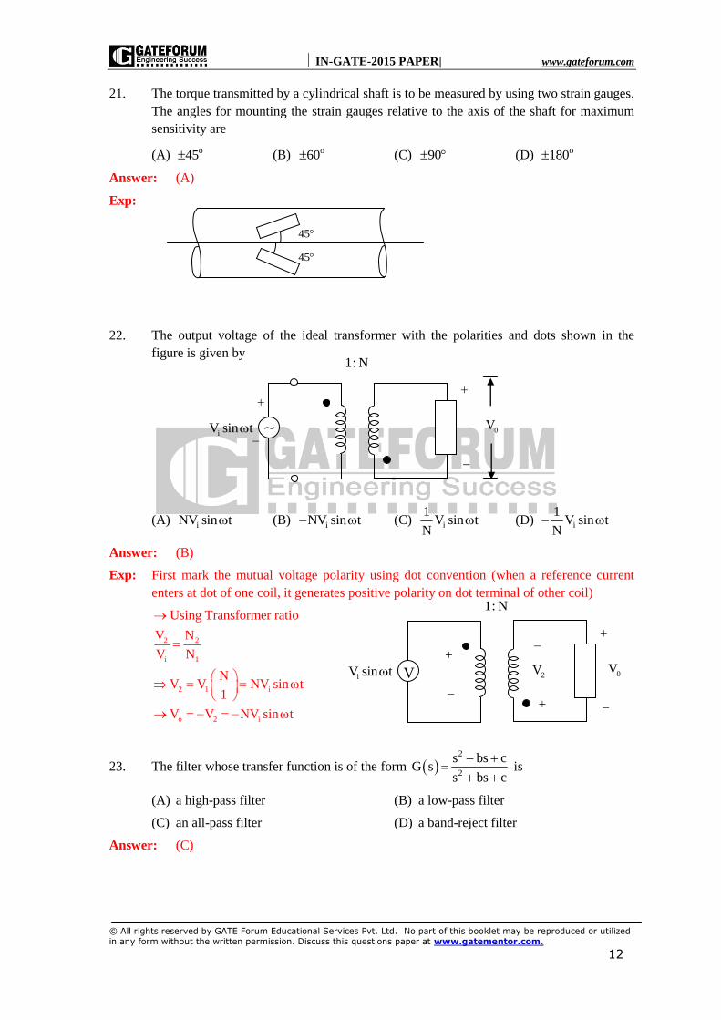
21. The torque transmitted by a cylindrical shaft is to be measured by using two strain gauges.
The angles for mounting the strain gauges relative to the axis of the shaft for maximum
sensitivity are
(A) o45 (B) o60 (C) 90 (D) o180
Answer: (A)
Exp:
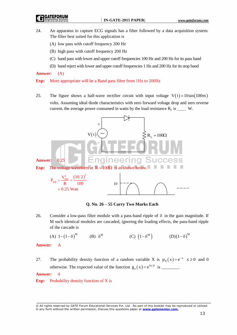
22. The output voltage of the ideal transformer with the polarities and dots shown in the
figure is given by
(A) iNV sin t (B) iNV sin t (C) i
1V sin t
N (D) i
1V sin t
N
Answer: (B)
Exp: First mark the mutual voltage polarity using dot convention (when a reference current
enters at dot of one coil, it generates positive polarity on dot terminal of other coil)
2 2
i 1
2 1 i
o 2 i
Using Transformer ratio
V N
V N
NV V NV sin t
1
V V NV sin t
23. The filter whose transfer function is of the form 2
2
s bs cG s
s bs c
is
(A) a high-pass filter (B) a low-pass filter
(C) an all-pass filter (D) a band-reject filter
Answer: (C)
0ViV sin t
1: N
0ViV sin t
1: N
2VV
45
45
IN-GATE-2015 PAPER| www.gateforum.com
© All rights reserved by GATE Forum Educational Services Pvt. Ltd. No part of this booklet may be reproduced or utilized
in any form without the written permission. Discuss this questions paper at www.gatementor.com.
13
24. An apparatus to capture ECG signals has a filter followed by a data acquisition system.
The filter best suited for this application is
(A) low pass with cutoff frequency 200 Hz
(B) high pass with cutoff frequency 200 Hz
(C) band pass with lower and upper cutoff frequencies 100 Hz and 200 Hz for its pass band
(D) band reject with lower and upper cutoff frequencies 1 Hz and 200 Hz for its stop band
Answer: (A)
Exp: More appropriate will be a Band pass filter from 1Hz to 200Hz
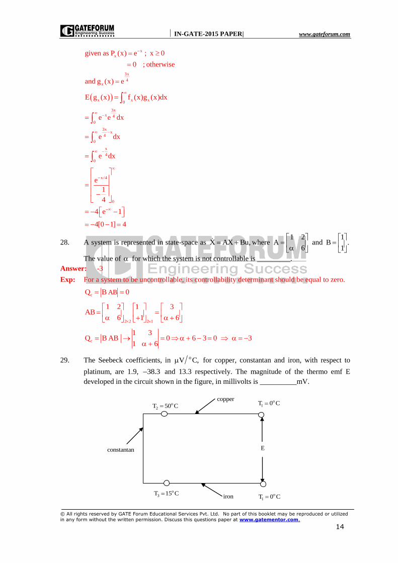
25. The figure shows a half-wave rectifier circuit with input voltage V t 10sin 100 t
volts. Assuming ideal diode characteristics with zero forward voltage drop and zero reverse
current, the average power consumed in watts by the load resistance RL is ____ W.
Answer: 0.25
Exp: The voltage waveform at R 100 is as shown below.
22
rmsavg
10 2VP
R 100
0.25 Watt
Q. No. 26 – 55 Carry Two Marks Each
26. Consider a low-pass filter module with a pass-band ripple of in the gain magnitude. If
M such identical modules are cascaded, ignoring the loading effects, the pass-band ripple
of the cascade is
(A) M
1 1 (B) M (C) M1 (D) M
1
Answer: A
27. The probability density function of a random variable X is xXp x e x 0 and 0
otherwise. The expected value of the function 3x 4xg x e is ________.
Answer: 4
Exp: Probability density function of X is
V t
LR 100
10
IN-GATE-2015 PAPER| www.gateforum.com
© All rights reserved by GATE Forum Educational Services Pvt. Ltd. No part of this booklet may be reproduced or utilized
in any form without the written permission. Discuss this questions paper at www.gatementor.com.
14
x
x
3x
4x
given as P (x) e ; x 0
0 ; otherwise
and g (x) e
x x x0
E g (x) f (x)g (x)dx
3x
x 4
0
3xx
4
0
x
4
0
e e dx
e dx
e dx
x /4
0
e
1
4
4 e 1
4[0 1] 4
28. A system is represented in state-space as X AX Bu, where 1 2
A6
and
1B .
1
The value of for which the system is not controllable is _________.
Answer: -3
Exp: For a system to be uncontrollable, its controllability determinant should be equal to zero.
c ABQ B 0
2 2 2 1
1 2 1 3AB
6 1 6
c
1 3Q B AB 0 6 3 0 3
1 6
29. The Seebeck coefficients, in oV C, for copper, constantan and iron, with respect to
platinum, are 1.9, 38.3 and 13.3 respectively. The magnitude of the thermo emf E
developed in the circuit shown in the figure, in millivolts is __________mV.
constantan
o2T 50 C
copper o1T 0 C
E
o3T 15 C
iron o1T 0 C
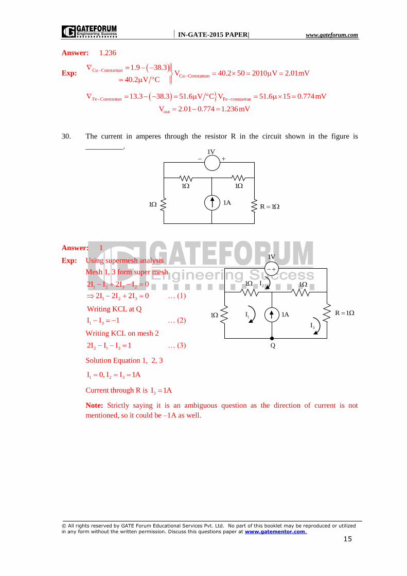
IN-GATE-2015 PAPER| www.gateforum.com
© All rights reserved by GATE Forum Educational Services Pvt. Ltd. No part of this booklet may be reproduced or utilized
in any form without the written permission. Discuss this questions paper at www.gatementor.com.
15
Answer: 1.236
Exp: Cu Constantan
Cu Constantan
1.9 38.3V 40.2 50 2010 V 2.01mV
40.2 V C
Fe Constantan Fe constantan
out
13.3 38.3 51.6 V C V 51.6 15 0.774mV
V 2.01 0.774 1.236mV
30. The current in amperes through the resistor R in the circuit shown in the figure is
__________.
Answer: 1
Exp: Using supermesh analysis
Mesh 1, 3 form super mesh
1 2 3 2
1 2 3
2I I 2I I 0
2I 2I 2I 0
… (1)
1 3
Writing KCL at Q
I I 1 … (2)
Writing KCL on mesh 2
2 1 32I I I 1 … (3)
Solution Equation 1, 2, 3
1 2 3I 0, I I 1A
Current through R is 3I 1A
Note: Strictly saying it is an ambiguous question as the direction of current is not
mentioned, so it could be –1A as well.
1 R 1
1 1
1V
1A
R 1 1A
1 1
1V
1I
3I
Q
2I
1
IN-GATE-2015 PAPER| www.gateforum.com
© All rights reserved by GATE Forum Educational Services Pvt. Ltd. No part of this booklet may be reproduced or utilized
in any form without the written permission. Discuss this questions paper at www.gatementor.com.
16
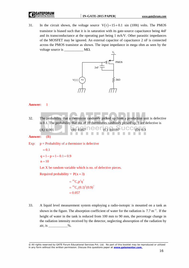
31. In the circuit shown, the voltage source V t 15 0.1 sin (100t) volts. The PMOS
transistor is biased such that it is in saturation with its gate-source capacitance being 4nF
and its transconductance at the operating part being 1 mA/V. Other parasitic impedances
of the MOSFET may be ignored. An external capacitor of capacitance 2 nF is connected
across the PMOS transistor as shown. The input impedance in mega ohm as seen by the
voltage source is ___________ M .
Answer: 1
32. The probability that a thermistor randomly picked up from a production unit is defective
is 0.1. The probability that out of 10 thermistors randomly picked up, 3 are defective is
(A) 0.001 (B) 0.057 (C) 0.0107 (D) 0.3
Answer: (B)
Exp: p = Probability of a thermister is defective
0.1
q 1 p 1 0.1 0.9
n 10
Let X be random variable which is no. of defective pieces.
Required probability = P(x 3)
10 3 7
3
10 3 7
3
C p q
C (0.1) (0.9)
0.057
33. A liquid level measurement system employing a radio-isotopic is mounted on a tank as
shown in the figure. The absorption coefficient of water for the radiation is 17.7 m . If the
height of water in the tank is reduced from 100 mm to 90 mm, the percentage change in
the radiation intensity received by the detector, neglecting abosroption of the radiation by
air, is ___________%.
V t ~
2nF
SV
PMOS
2k

IN-GATE-2015 PAPER| www.gateforum.com
© All rights reserved by GATE Forum Educational Services Pvt. Ltd. No part of this booklet may be reproduced or utilized
in any form without the written permission. Discuss this questions paper at www.gatementor.com.
17
Answer: 8
Exp: General formula for the amount of intensity received , xoI I e
I0 Intensity when absorbing material is nill or empty
absorption coefficient
density of the absorption material
x thickness (or) height of the absorbing, material
By considering the given parameters and neglecting others
Intensity received,
(a) When xheight = 100 mm = 0.1 m
7.7 0.1 0.77
1I e e
(b) When x = 90 mm = 0.9 m
7.7 0.09 0.693
2I e e
So, 2 1
1
I Ichange%change 100 100 8%
Initial I
34. A beam of monochromatic light passes through two glass slabs of the same geometrical
thickness at normal incidence. The refractive index of the first slab is 1.5 and that of the
second, 2.0. The ratio of the time of passage of the beam through the first to the second
slab is _________.
Answer: 0.75
Exp: We know, distance d
timevelocity v
Detector
Source
Water
IN-GATE-2015 PAPER| www.gateforum.com
© All rights reserved by GATE Forum Educational Services Pvt. Ltd. No part of this booklet may be reproduced or utilized
in any form without the written permission. Discuss this questions paper at www.gatementor.com.
18
∴ The ratio of the time for 2 slabs 1
2
t
t
1 21 1 1 2
2 2 1 2
2
1
2 2
1 1
1
2
d d becauseof samed v d v
d v v d geometrical thickness
v
v
v
v
1.5
2.0
0.75
NOTE: If a light of velocity “v” is passing through a matter of R.I = 0.7 (say)
Then the final output velocity will be v
0.7
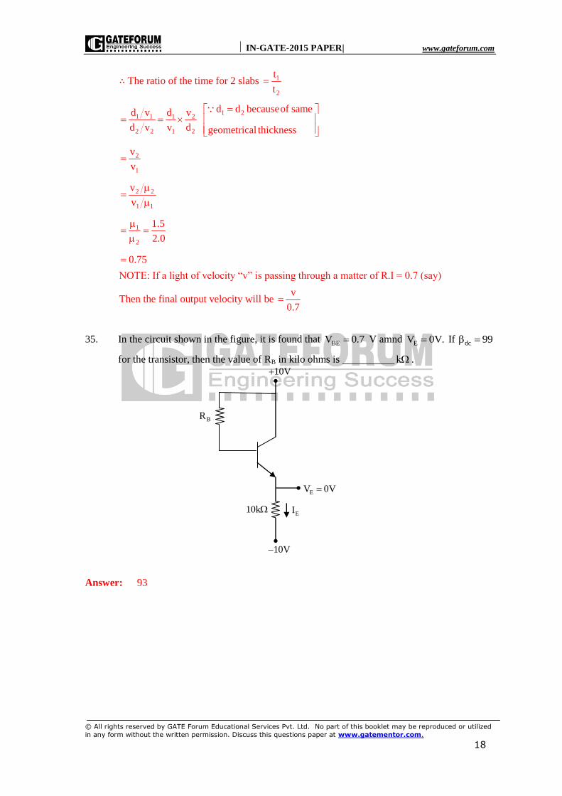
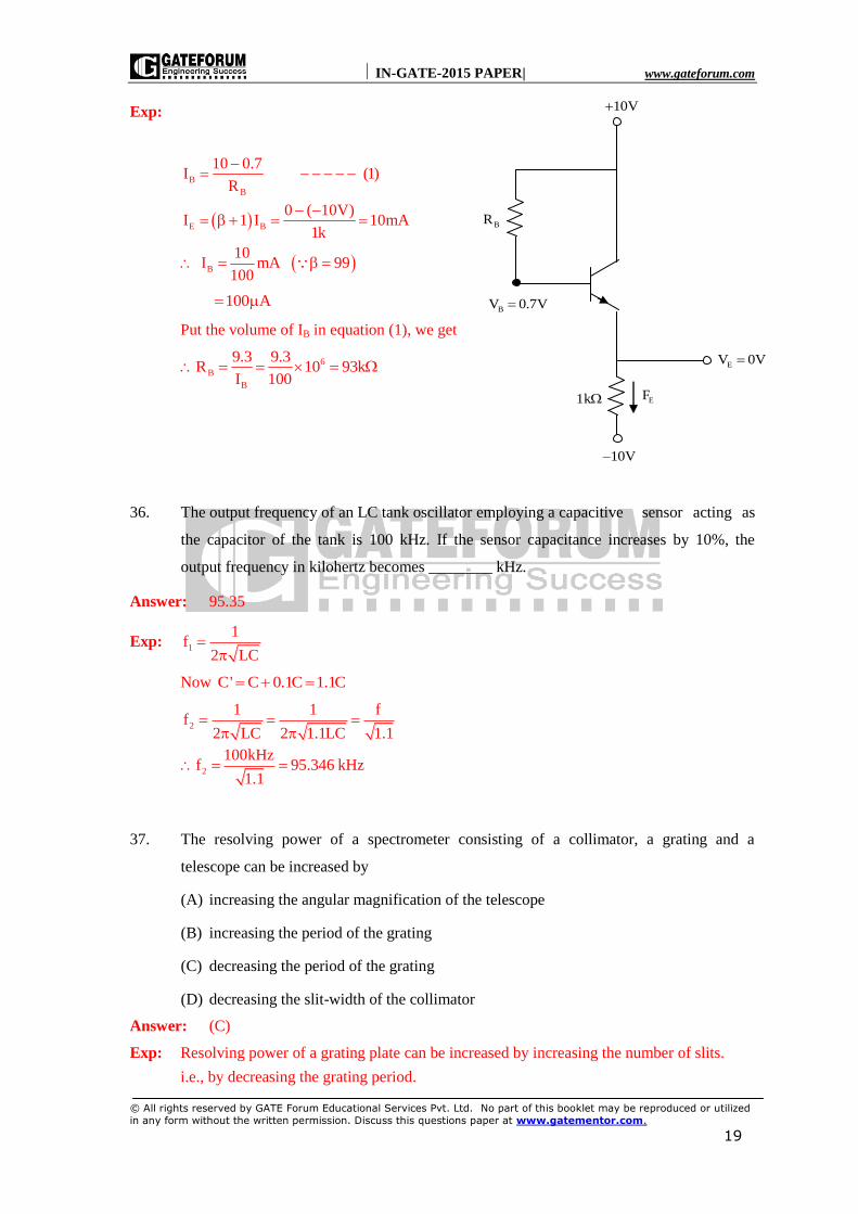
35. In the circuit shown in the figure, it is found that BEV 0.7 V amnd EV 0V. If dc 99
for the transistor, then the value of RB in kilo ohms is __________ k .
Answer: 93
BR
10kEI
10V
EV 0V
10V
IN-GATE-2015 PAPER| www.gateforum.com
© All rights reserved by GATE Forum Educational Services Pvt. Ltd. No part of this booklet may be reproduced or utilized
in any form without the written permission. Discuss this questions paper at www.gatementor.com.
19
Exp:
B
B
E B
B
10 0.7I (1)
R
0 ( 10V)I 1 I 10mA
1k
10I mA 99
100
100 A
Put the volume of IB in equation (1), we get
6
B
B
9.3 9.3R 10 93k
I 100
36. The output frequency of an LC tank oscillator employing a capacitive sensor acting as
the capacitor of the tank is 100 kHz. If the sensor capacitance increases by 10%, the
output frequency in kilohertz becomes ________ kHz.
Answer: 95.35
Exp: 1
1f
2 LC
Now C' C 0.1C 1.1C
2
2
1 1 ff
2 LC 2 1.1LC 1.1
100kHzf 95.346 kHz
1.1
37. The resolving power of a spectrometer consisting of a collimator, a grating and a
telescope can be increased by
(A) increasing the angular magnification of the telescope
(B) increasing the period of the grating
(C) decreasing the period of the grating
(D) decreasing the slit-width of the collimator
Answer: (C)
Exp: Resolving power of a grating plate can be increased by increasing the number of slits.
i.e., by decreasing the grating period.
10V
1k EF
EV 0V
BV 0.7V
BR
10V
IN-GATE-2015 PAPER| www.gateforum.com
© All rights reserved by GATE Forum Educational Services Pvt. Ltd. No part of this booklet may be reproduced or utilized
in any form without the written permission. Discuss this questions paper at www.gatementor.com.
20
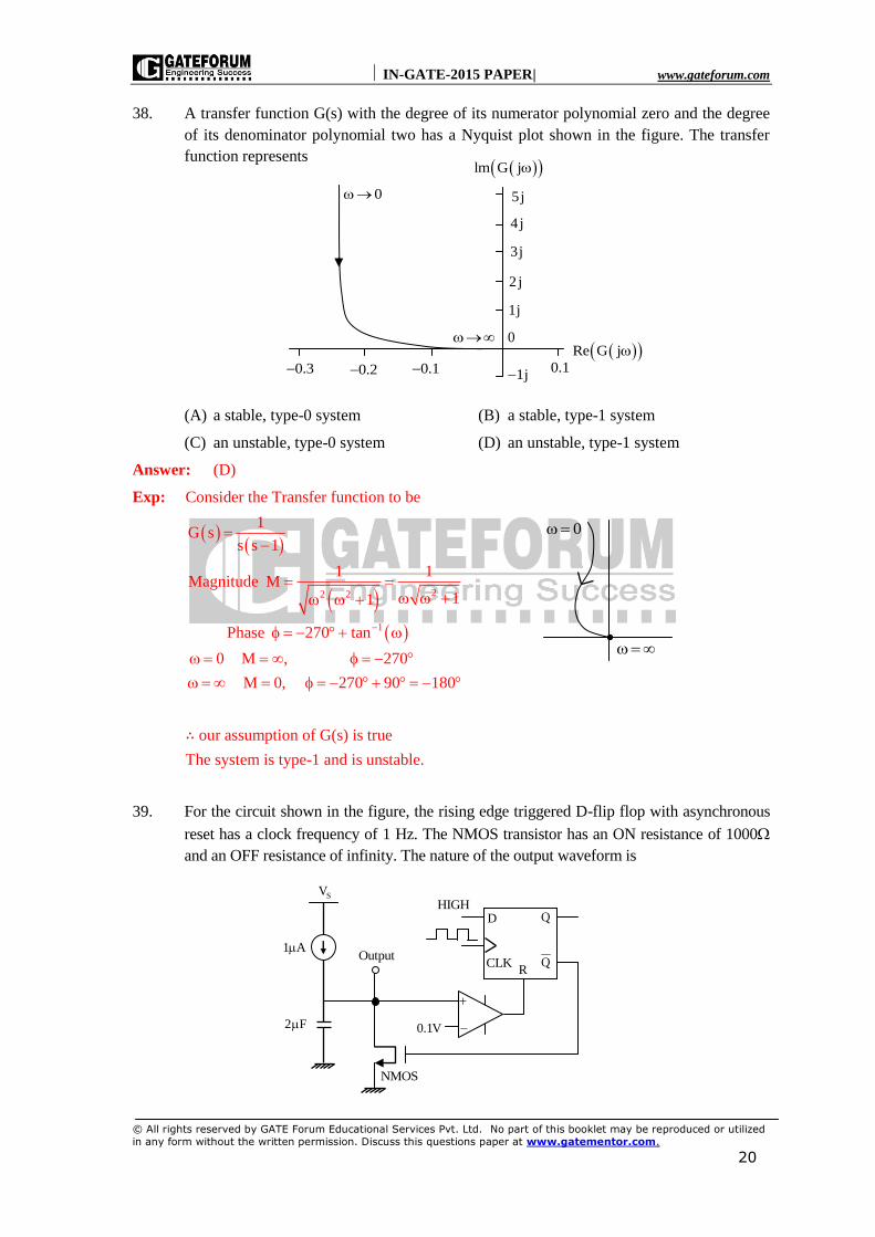
38. A transfer function G(s) with the degree of its numerator polynomial zero and the degree
of its denominator polynomial two has a Nyquist plot shown in the figure. The transfer
function represents
(A) a stable, type-0 system (B) a stable, type-1 system
(C) an unstable, type-0 system (D) an unstable, type-1 system
Answer: (D)
Exp: Consider the Transfer function to be
22 2
1
1G s
s s 1
1 1Magnitude M
11
Phase 270 tan
0 M , 270
M 0, 270 90 180
∴ our assumption of G(s) is true
The system is type-1 and is unstable.
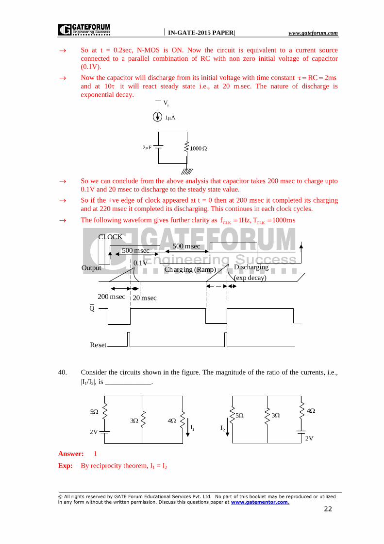
39. For the circuit shown in the figure, the rising edge triggered D-flip flop with asynchronous
reset has a clock frequency of 1 Hz. The NMOS transistor has an ON resistance of 1000
and an OFF resistance of infinity. The nature of the output waveform is
0
lm G j
5j
4 j
3j
2 j
1j
1j0.20.3 0.1 0.1
0 Re G j
1 A
2 F 0.1V
SVHIGH
CLKR
Q
QD
Output
NMOS
0

IN-GATE-2015 PAPER| www.gateforum.com
© All rights reserved by GATE Forum Educational Services Pvt. Ltd. No part of this booklet may be reproduced or utilized
in any form without the written permission. Discuss this questions paper at www.gatementor.com.
21
A
B
C
D
Answer: (A)
Exp: Before solving the problem, consider the following fact.
clock is +ve edge triggered and input to D flip-flop is constant i.e logic 1.
Reset pin of Flip flip is active high and it can function at any moment of time
independent to clock. Also note that reset will be triggered when V terminal voltage just
crosses 0.1 V.
N-MOS behave as open switch (off state, R ) when Q 0 and it will behave as a
resistance of 1000 when Q 1 (as ON resistance is specified).
Now for analysis, assume capacitor is initially uncharged and a +ve edge is triggered
to D-flipflop, as its input is high. Then Q=1 and Q 0 .
* When Q 0 , N-MOS is off, assuming the input resistance of comparator infinite. Then
the source current can flow only through the capacitor. Now we have to see how much
time the capacitor will take to reach 0.1 V. So that V V and R will change from 0 to 1
and as the reset terminal will be triggered the state of flip-flop changes i.e. Q 0, Q 1 .
and N-MOS gets ON. As the integration of step is ramp if we integrate the constant
current voltage will be ramp.
For this use the capacitor voltage equation.
t
c c0
t6
6 0
1V (t) i d
C
10.1V 1 10 d
2 10
t0.1 t 0.2sec 200 millisec
2
0V
1 A
2 F
0V
IN-GATE-2015 PAPER| www.gateforum.com
© All rights reserved by GATE Forum Educational Services Pvt. Ltd. No part of this booklet may be reproduced or utilized
in any form without the written permission. Discuss this questions paper at www.gatementor.com.
22
So at t = 0.2sec, N-MOS is ON. Now the circuit is equivalent to a current source
connected to a parallel combination of RC with non zero initial voltage of capacitor
(0.1V).
Now the capacitor will discharge from its initial voltage with time constant RC 2ms
and at 10 it will react steady state i.e., at 20 m.sec. The nature of discharge is
exponential decay.
So we can conclude from the above analysis that capacitor takes 200 msec to charge upto
0.1V and 20 msec to discharge to the steady state value.
So if the +ve edge of clock appeared at t = 0 then at 200 msec it completed its charging
and at 220 msec it completed its discharging. This continues in each clock cycles.
The following waveform gives further clarity as CLK CLKf 1Hz, T 1000ms
40. Consider the circuits shown in the figure. The magnitude of the ratio of the currents, i.e.,
|I1/I2|, is _____________.
Answer: 1
Exp: By reciprocity theorem, I1 = I2
5
2V2V
5 34
43
2I1I
1 A
2 F
sV
1000
500 msec500 msec
CLOCK
Output
200 msec 20 msec
Charging (Ramp) Discharging
(exp decay)
Q
0.1V
Reset
IN-GATE-2015 PAPER| www.gateforum.com
© All rights reserved by GATE Forum Educational Services Pvt. Ltd. No part of this booklet may be reproduced or utilized
in any form without the written permission. Discuss this questions paper at www.gatementor.com.
23
So 1
2
I1
I
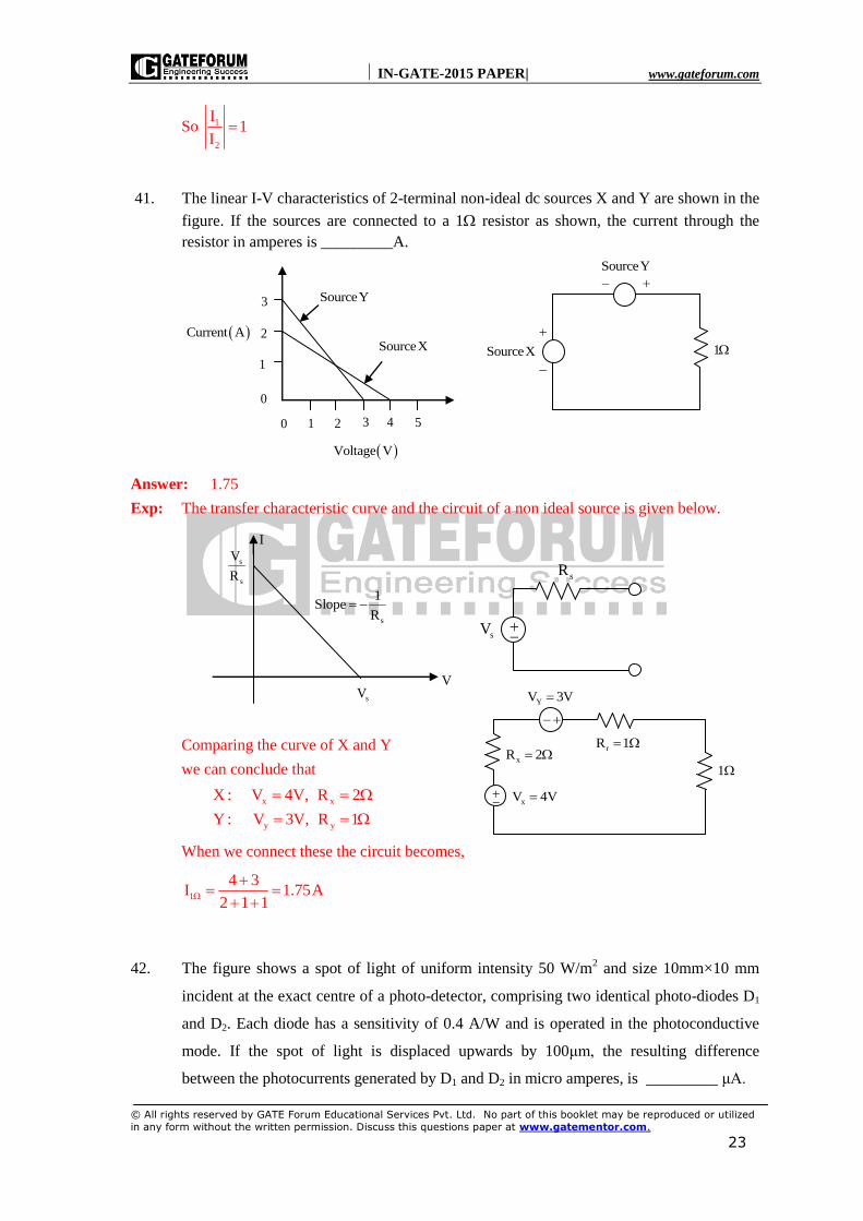
41. The linear I-V characteristics of 2-terminal non-ideal dc sources X and Y are shown in the
figure. If the sources are connected to a 1 resistor as shown, the current through the
resistor in amperes is _________A.
Answer: 1.75
Exp: The transfer characteristic curve and the circuit of a non ideal source is given below.
Comparing the curve of X and Y
we can conclude that
x x
y y
X : V 4V, R 2
Y : V 3V, R 1
When we connect these the circuit becomes,
1
4 3I 1.75A
2 1 1
42. The figure shows a spot of light of uniform intensity 50 W/m2 and size 10mm×10 mm
incident at the exact centre of a photo-detector, comprising two identical photo-diodes D1
and D2. Each diode has a sensitivity of 0.4 A/W and is operated in the photoconductive
mode. If the spot of light is displaced upwards by 100μm, the resulting difference
between the photocurrents generated by D1 and D2 in micro amperes, is _________ μA.
SourceY
SourceX
Voltage V
Current A
1
2
3
0
0 1 2 3 54
SourceX
SourceY
1
1
xV 4V
YV 3V
rR 1 xR 2
sV
s
s
V
R
s
1Slope
R
V
I
sV
sR

IN-GATE-2015 PAPER| www.gateforum.com
© All rights reserved by GATE Forum Educational Services Pvt. Ltd. No part of this booklet may be reproduced or utilized
in any form without the written permission. Discuss this questions paper at www.gatementor.com.
24
Answer: 40
Exp: Total illuminated Area = 10×10×10-6
m2 = 10
-4m
2
Light power = 50×10-4
W = 5mW
Output from both diodes = 0.4×5mA = 2mA
So output from each diode = 1mA
In second case,
Area of one diode (D1) = 10×5.1×10-6
= 0.51×10⁻⁴
m2
Light output (D1) = 0.51×10-4
×50W
= 2.55 mW
Current in D1 = 2.55×0.4 = 1.02 mA
Current in D2 = Total current – ID1
= 2-1.02 = 0.98 mA
D1 D2I I 1.02 0.98 mA 0.04mA 40 A
1D
2D
Photo-
detector
10mm
10mm
Spot of
light
IN-GATE-2015 PAPER| www.gateforum.com
© All rights reserved by GATE Forum Educational Services Pvt. Ltd. No part of this booklet may be reproduced or utilized
in any form without the written permission. Discuss this questions paper at www.gatementor.com.
25
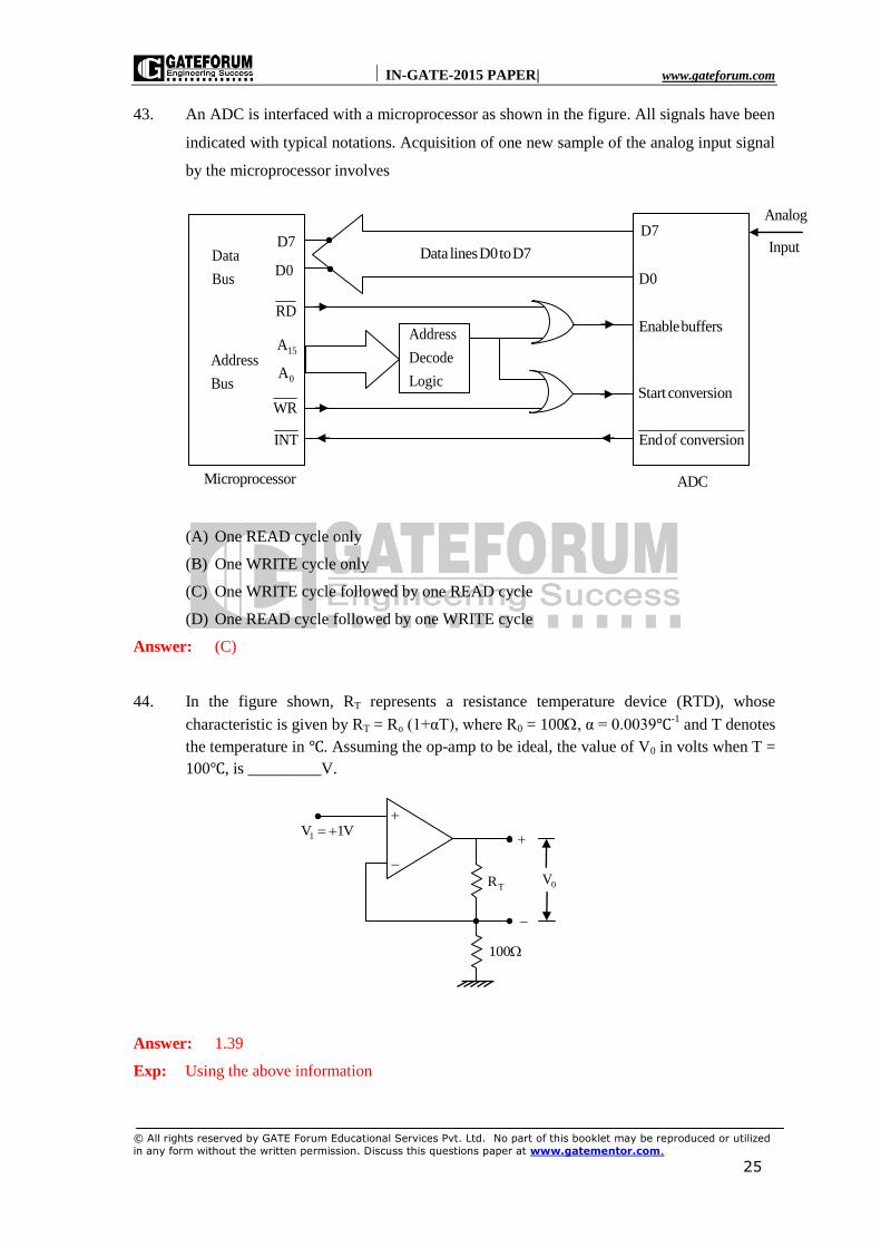
43. An ADC is interfaced with a microprocessor as shown in the figure. All signals have been
indicated with typical notations. Acquisition of one new sample of the analog input signal
by the microprocessor involves
(A) One READ cycle only
(B) One WRITE cycle only
(C) One WRITE cycle followed by one READ cycle
(D) One READ cycle followed by one WRITE cycle
Answer: (C)
44. In the figure shown, RT represents a resistance temperature device (RTD), whose
characteristic is given by RT = Ro (1+αT), where R0 = 100, α = 0.0039℃-1 and T denotes
the temperature in ℃. Assuming the op-amp to be ideal, the value of V0 in volts when T =
100℃, is _________V.
Answer: 1.39
Exp: Using the above information
1V 1V
TR
100
0V
Data linesD0toD7
Address
Decode
Logic
D7
D0
Enablebuffers
Start conversion
Endof conversion
Data
Bus
Address
Bus
D7
D0
RD
15A
0A
WR
INT
Analog
Input
ADCMicroprocessor

IN-GATE-2015 PAPER| www.gateforum.com
© All rights reserved by GATE Forum Educational Services Pvt. Ltd. No part of this booklet may be reproduced or utilized
in any form without the written permission. Discuss this questions paper at www.gatementor.com.
26
T oR R 1 T
100 1 0.0039 100 139
Since it is a non inverting amplifier its output voltage w.r.t ground is
fi
i
R 1391 V 1 2.39V
R 100
But here Vo is not w.r.t ground, it is across RT
So oV 2.39 1 1.39V
45. The signal x[n] = sin(πn/6)/(πn) is processed through a linear filter with the impulse
response h[n] = sin(cn)/(πn) where c>π/6. The output of the filter is
(A) sin(2cn)/(πn) (2) sin(πn/3)/(πn)
(C) [sin(πn/6)/(πn)]2
(D) [sin(πn/6)/(πn)]
Answer: (D)
Exp:
sin n sin n sin n
n n n
where min ,
Output g n x n *h n
In frequency domain they will be multiplied.
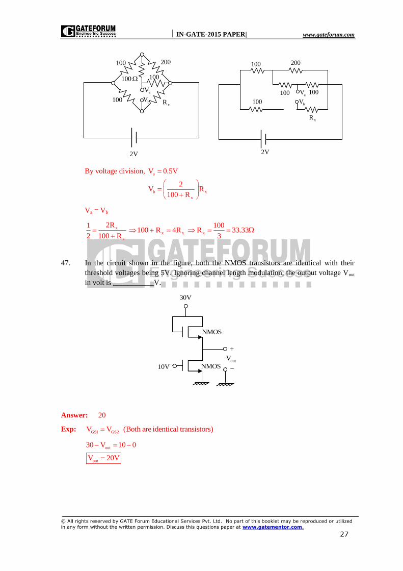
46. If the deflection of the galvanometer in the bridge circuit shown in the figure is zero, then
the value of Rx in ohms is ________ . .
Answer: 33.33
Exp: When the current through galvanometer is 0 then its 2 end voltage are same or we can say
the open circuit voltage across galvanometer is 0.
100 200
100 xR
100
G50
2V
100
IN-GATE-2015 PAPER| www.gateforum.com
© All rights reserved by GATE Forum Educational Services Pvt. Ltd. No part of this booklet may be reproduced or utilized
in any form without the written permission. Discuss this questions paper at www.gatementor.com.
27
By voltage division, a
b x
x
V 0.5V
2V R
100 R
Va = Vb
x
x x x
x
2R1 100100 R 4R R 33.33
2 100 R 3
47. In the circuit shown in the figure, both the NMOS transistors are identical with their
threshold voltages being 5V. Ignoring channel length modulation, the output voltage Vout
in volt is ___________V.
Answer: 20
Exp: GS1 GS2V V (Both are identical transistors)
out
out
30 V 10 0
V 20V
30V
10V
NMOS
NMOSoutV
100 200
100xR
100
2V
aV
bV
100
100
100
200
100
xR
100
aV
bV
2V
IN-GATE-2015 PAPER| www.gateforum.com
© All rights reserved by GATE Forum Educational Services Pvt. Ltd. No part of this booklet may be reproduced or utilized
in any form without the written permission. Discuss this questions paper at www.gatementor.com.
28
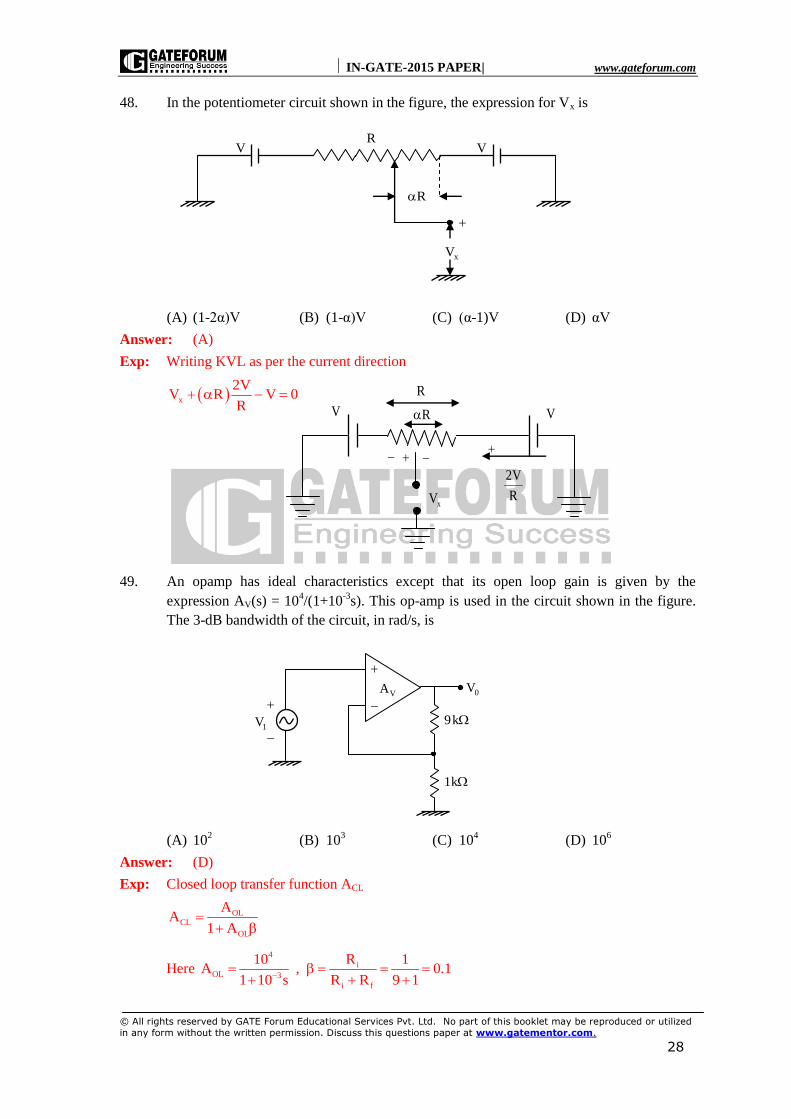
48. In the potentiometer circuit shown in the figure, the expression for Vx is
(A) (1-2α)V (B) (1-α)V (C) (α-1)V (D) αV
Answer: (A)
Exp: Writing KVL as per the current direction
x
2VV R V 0
R
49. An opamp has ideal characteristics except that its open loop gain is given by the
expression AV(s) = 104/(1+10
-3s). This op-amp is used in the circuit shown in the figure.
The 3-dB bandwidth of the circuit, in rad/s, is
(A) 102 (B) 10
3 (C) 10
4 (D) 10
6
Answer: (D)
Exp: Closed loop transfer function ACL
OLCL
OL
AA
1 A
Here 4
iOL 3
i f
R10 1A , 0.1
1 10 s R R 9 1
1V
0V
9k
1k
VA
V VR
R
xV
R
R
xV
V
V
2V
R

IN-GATE-2015 PAPER| www.gateforum.com
© All rights reserved by GATE Forum Educational Services Pvt. Ltd. No part of this booklet may be reproduced or utilized
in any form without the written permission. Discuss this questions paper at www.gatementor.com.
29
4
43
CL 4 3 3
3
3 6
6
10
101 10 sA10 0.1 1 10 s 10
11 10 s
10 10
s10 10 s 11
10
In a first order transfer function k
1 s
the bandwidth of system is given by 1
6B.W 10
50. A signal is band-limited to 0 to 12 kHz. The signal spectrum is corrupted by additive
noise which is band-limited to 10 to 12 kHz. Theoretically, the minimum rate in kilohertz
at which the noisy signal must be sampled so that the UNCORRUPTED PART of the
signal spectrum can be recovered, is _________ kHz.
Answer: 22
Exp:
The signal is corrupted from 10 to 12 kHz. So the ideal sampling,
s s
n
X (f ) X f nf
If Fs= 20 kHz then the spectrum will be
So the overlapping is starting from 8 kHz onwards, but we want it should be from 10 kHz
onward because the uncorrupted is up to 10 kHz.
So the sampling frequency should increase by 2kHz.
So sf 20 2 22kHz, the spectrum.
32 8 8 1212 32
12 10 10 12
IN-GATE-2015 PAPER| www.gateforum.com
© All rights reserved by GATE Forum Educational Services Pvt. Ltd. No part of this booklet may be reproduced or utilized
in any form without the written permission. Discuss this questions paper at www.gatementor.com.
30
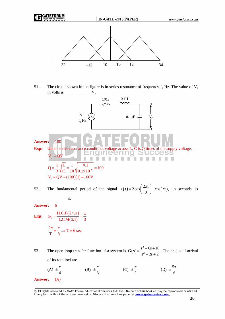
51. The circuit shown in the figure is in series resonance of frequency fc Hz. The value of Vc
in volts is _____________V.
Answer: 100
Exp: Under series resonance condition, voltage across L, C is Q times of the supply voltage.
CV QV
6
c
1 L 1 0.1Q 100
R C 10 0.1 10
V QV 100 1 100V
52. The fundamental period of the signal 2 t
x t 2cos cos t ,3
in seconds, is
__________s.
Answer: 6
Exp:
0
H.C.F 2 ,
L.C.M 3,1 3
2
T 6 secT 3
53. The open loop transfer function of a system is 2
2
s 6s 10G s .
s 2s 2
The angles of arrival
of its root loci are
(A) 4
(B)
3
(C)
2
(D)
5
6
Answer: (A)
10 0.1H
0.1 F CV
c
1V
f Hz
32 10 1212 3410

IN-GATE-2015 PAPER| www.gateforum.com
© All rights reserved by GATE Forum Educational Services Pvt. Ltd. No part of this booklet may be reproduced or utilized
in any form without the written permission. Discuss this questions paper at www.gatementor.com.
31
Exp: Angle of arrival is calculated on a complex zero and it is given by,
a 180 GH at a ve imaginary zero
s 3 i s 3 iG s
s 1 i s 1 i
3 i 3 i 3 i 3 i 2iG 3 i
3 i 1 i 3 i 1 i 2 2i 2
o o 1 o
o o o o o
2G 3 i 90 180 tan 180
2
90 180 45 180 135
a 180 135 454
Other angle will be same with opposite sign 4
54. The z-transform of x[n] = a|n|
, 0<|α|<1, is X(z). The region of convergence of X(z) is
(A) 1
z
(B) |z|>a
(C) 1
z
(D) 1
z min ,
Answer: (A)
Exp: n
n n 1x n u n u n 1
1z ; z
x x 1
IN-GATE-2015 PAPER| www.gateforum.com
© All rights reserved by GATE Forum Educational Services Pvt. Ltd. No part of this booklet may be reproduced or utilized
in any form without the written permission. Discuss this questions paper at www.gatementor.com.
32
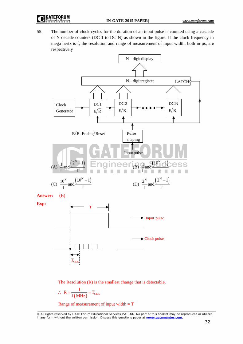
55. The number of clock cycles for the duration of an input pulse is counted using a cascade
of N decade counters (DC 1 to DC N) as shown in the figure. If the clock frequency in
mega hertz is f, the resolution and range of measurement of input width, both in μs, are
respectively
(A) N2 11
andf f
(B)
N10 11and
f f
(C) NN 10 110
andf f
(D)
NN 2 12and
f f
Answer: (B)
Exp:
The Resolution (R) is the smallest change that is detectable.
CLK
1R T
f MHz
Range of measurement of input width = T
N digitdisplay
N digit register LATCH
Clock
Generator
DC1
E R
DC2
E R
DC N
E R
Pulse
shaping
Input pulse
E R :Enable Reset
CLKT
T
Input pulse
Clock pulse

IN-GATE-2015 PAPER| www.gateforum.com
© All rights reserved by GATE Forum Educational Services Pvt. Ltd. No part of this booklet may be reproduced or utilized
in any form without the written permission. Discuss this questions paper at www.gatementor.com.
33
NCLK
N
T 10 1 T
10 1T
f