Embed Size (px)
Citation preview
Deep Sea Electronics plc,Highfield House,Hunmanby Industrial Estate,North Yorkshire YO14 0PH,England
Deep Sea Electronics plc reserve the right to change the GenComm standard at any time and without notice.Deep Sea Electronics plc own the copyright for the GenComm standard.All rights reserved.
GenComm standard for use with generating set control equipment
Author: G. MiddletonVersion: 2.14 Revision date: 16/04/2012 by DJRFilename: GenComm.docx
Table of contents
1. Changes from previous version 22. Introduction 43. General Definitions and Requirements 44. Hubs and Protocol Conversions 55. Multiple Masters 56. Exception Responses67. Modbus Functions Used 88. Description of Each Function 8
8.1 Function 3 - Read Multiple Registers 88.2 Function 16 - Write Multiple Registers 10
9. Language Codes 1110. Modbus Registers Defined 15
10.1 Index of Register Pages 1510.2 Page 0 - Communications Status Information 1710.3 Page 1 - Communications Configuration 2010.4 Page 2 - Modem Configuration 2210.5 Page 3 - Generating Set Status Information 2310.6 Page 4 - Basic Instrumentation 2610.7 Page 5 - Extended Instrumentation 2910.8 Page 6 - Derived Instrumentation 3310.9 Page 7 - Accumulated Instrumentation 3610.10 Page 8 - Alarm Conditions 3810.11 Page 9 – Total Harmonic Distortion 4210.12 Page 11 - Diagnostic - General 4310.13 Page 12 - Diagnostic - Digital Inputs 4310.14 Page 13 - Diagnostic - Digital Outputs 4510.15 Page 14 - Diagnostic - LEDs 4610.16 Page 16 - Control Registers 4810.17 Page 17 - J1939 active diagnostic trouble codes in decoded format 5010.18 Page 18 - J1939 active diagnostic trouble codes in raw format 5210.19 Page 20 - Various Strings 5310.20 Page 22- Auxiliary sender strings 5310.21 Page 24 - Identity Strings 5310.22 Page 26 - State Machine Name Strings 5410.23 Page 28 - State Machine State Strings 5410.24 Pages 32 to 95 - Alarm Strings (Old alarm system) 5510.25 Pages 32-36 - 2131 Expansion module name strings 61
Page 1
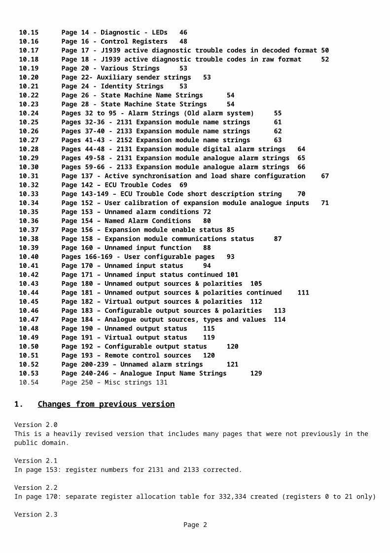
10.26 Pages 37-40 - 2133 Expansion module name strings 6210.27 Pages 41-43 - 2152 Expansion module name strings 6310.28 Pages 44-48 - 2131 Expansion module digital alarm strings 6410.29 Pages 49-58 - 2131 Expansion module analogue alarm strings 6510.30 Pages 59-66 - 2133 Expansion module analogue alarm strings 6610.31 Page 137 - Active synchronisation and load share configuration 6710.32 Page 142 – ECU Trouble Codes 6910.33 Page 143-149 – ECU Trouble Code short description string7010.34 Page 152 – User calibration of expansion module analogue inputs 7110.35 Page 153 – Unnamed alarm conditions 7210.36 Page 154 – Named Alarm Conditions 8010.37 Page 156 – Expansion module enable status 8510.38 Page 158 – Expansion module communications status 8710.39 Page 160 – Unnamed input function 8810.40 Pages 166-169 - User configurable pages 9310.41 Page 170 – Unnamed input status 9410.42 Page 171 – Unnamed input status continued 10110.43 Page 180 – Unnamed output sources & polarities 10510.44 Page 181 – Unnamed output sources & polarities continued 11110.45 Page 182 – Virtual output sources & polarities 11210.46 Page 183 – Configurable output sources & polarities 11310.47 Page 184 – Analogue output sources, types and values 11410.48 Page 190 – Unnamed output status 11510.49 Page 191 – Virtual output status 11910.50 Page 192 – Configurable output status 12010.51 Page 193 – Remote control sources 12010.52 Page 200-239 – Unnamed alarm strings 12110.53 Page 240-246 – Analogue Input Name Strings 12910.54 Page 250 – Misc strings 131
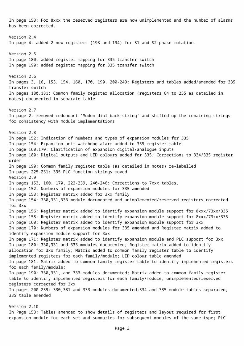
1. Changes from previous version
Version 2.0This is a heavily revised version that includes many pages that were not previously in the public domain.
Version 2.1In page 153: register numbers for 2131 and 2133 corrected.
Version 2.2In page 170: separate register allocation table for 332,334 created (registers 0 to 21 only)
Version 2.3In page 153: For 8xxx the reserved registers are now unimplemented and the number of alarms has been corrected.
Version 2.4In page 4: added 2 new registers (193 and 194) for S1 and S2 phase rotation.
Version 2.5In page 180: added register mapping for 335 transfer switchIn page 190: added register mapping for 335 transfer switch
Version 2.6In pages 3, 16, 153, 154, 160, 170, 190, 200-249: Registers and tables added/amended for 335 transfer switchIn pages 180,181: Common family register allocation (registers 64 to 255 as detailed in notes) documented in separate table
Version 2.7In page 2: removed redundant ‘Modem dial back string’ and shifted up the remaining strings for consistency with module implementations
Version 2.8In page 152: Indication of numbers and types of expansion modules for 335In page 154: Expansion unit watchdog alarm added to 335 register tableIn page 160,170: Clarification of expansion digital/analogue inputsIn page 180: Digital outputs and LED colours added for 335; Corrections to 334/335 register order
Page 2
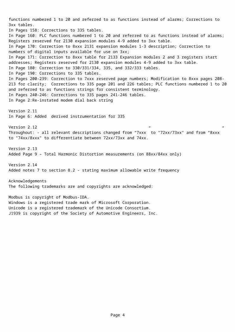
In page 190: Common family register table (as detailed in notes) re-labelled In pages 225-231: 335 PLC function strings movedVersion 2.9In pages 153, 160, 170, 222-239, 240-246: Corrections to 7xxx tables.In page 152: Numbers of expansion modules for 335 amendedIn page 153: Register matrix added for 3xx familyIn page 154: 330,331,333 module documented and unimplemented/reserved registers corrected for 3xxIn page 156: Register matrix added to identify expansion module support for 8xxx/73xx/335In page 158: Register matrix added to identify expansion module support for 8xxx/73xx/335In page 160: Register matrix added to identify expansion module support for 3xxIn page 170: Numbers of expansion modules for 335 amended and Register matrix added to identify expansion module support for 3xxIn page 171: Register matrix added to identify expansion module and PLC support for 3xxIn page 180: 330,331 and 333 modules documented; Register matrix added to identify allocation for 3xx family; Matrix added to common family register table to identify implemented registers for each family/module; LED colour table amendedIn page 181: Matrix added to common family register table to identify implemented registers for each family/module;In page 190: 330,331, and 333 modules documented; Matrix added to common family register table to identify implemented registers for each family/module; unimplemented/reserved registers corrected for 3xxIn pages 200-239: 330,331 and 333 modules documented;334 and 335 module tables separated; 335 table amended
Version 2.10In Page 153: Tables amended to show details of registers and layout required for first expansion module for each set and summaries for subsequent modules of the same type; PLC functions numbered 1 to 20 and referred to as functions instead of alarms; Corrections to 3xx tables.In Pages 158: Corrections to 335 tables.In Page 160: PLC functions numbered 1 to 20 and referred to as functions instead of alarms; Registers reserved for 2130 expansion modules 4-9 added to 3xx table.In Page 170: Correction to 8xxx 2131 expansion modules 1-3 description; Correction to numbers of digital inputs available for use on 3xx; In Page 171: Correction to 8xxx table for 2133 Expansion modules 2 and 3 registers start addresses; Registers reserved for 2130 expansion modules 4-9 added to 3xx table.In Page 180: Correction to 330/331/334, 335, and 332/333 tables.In Page 190: Corrections to 335 tables.In Pages 200-239: Correction to 7xxx reserved page numbers; Modification to 8xxx pages 208-213 for clarity; Corrections to 335 page 201 and 226 tables; PLC functions numbered 1 to 20 and referred to as functions strings for consistent terminology.In Pages 240-246: Corrections to 335 pages 241-246 tables.In Page 2:Re-instated modem dial back string
Version 2.11In Page 6: Added derived instrumentation for 335
Version 2.12Throughout: - all relevant descriptions changed from “7xxx” to "72xx/73xx" and from “8xxx” to "74xx/8xxx" to differentiate between 72xx/73xx and 74xx.
Version 2.13Added Page 9 – Total Harmonic Distortion measurements (on 88xx/84xx only)
Version 2.14Added notes 7 to section 8.2 - stating maximum allowable write frequency
AcknowledgementsThe following trademarks are and copyrights are acknowledged:
Modbus is copyright of Modbus-IDA.Windows is a registered trade mark of Microsoft Corporation.Unicode is a registered trademark of the Unicode Consortium.J1939 is copyright of the Society of Automotive Engineers, Inc.
Page 3
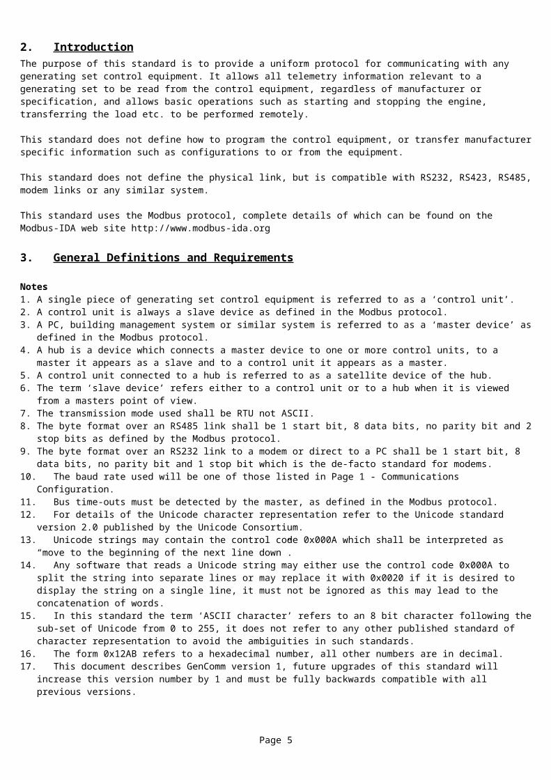
2. Introduction The purpose of this standard is to provide a uniform protocol for communicating with any generating set control equipment. It allows all telemetry information relevant to a generating set to be read from the control equipment, regardless of manufacturer or specification, and allows basic operations such as starting and stopping the engine, transferring the load etc. to be performed remotely.
This standard does not define how to program the control equipment, or transfer manufacturer specific information such as configurations to or from the equipment.
This standard does not define the physical link, but is compatible with RS232, RS423, RS485, modem links or any similar system.
This standard uses the Modbus protocol, complete details of which can be found on the Modbus-IDA web site http://www.modbus-ida.org
3. General Definitions and Requirements
Notes1. A single piece of generating set control equipment is referred to as a ‘control unit’.2. A control unit is always a slave device as defined in the Modbus protocol.3. A PC, building management system or similar system is referred to as a ‘master device’ as defined in the Modbus protocol.4. A hub is a device which connects a master device to one or more control units, to a master it appears as a slave and to a control unit
it appears as a master.5. A control unit connected to a hub is referred to as a satellite device of the hub.6. The term ‘slave device’ refers either to a control unit or to a hub when it is viewed from a masters point of view.7. The transmission mode used shall be RTU not ASCII.8. The byte format over an RS485 link shall be 1 start bit, 8 data bits, no parity bit and 2 stop bits as defined by the Modbus protocol.9. The byte format over an RS232 link to a modem or direct to a PC shall be 1 start bit, 8 data bits, no parity bit and 1 stop bit which is
the de-facto standard for modems.10. The baud rate used will be one of those listed in Page 1 - Communications Configuration.11. Bus time-outs must be detected by the master, as defined in the Modbus protocol.12. For details of the Unicode character representation refer to the Unicode standard version 2.0 published by the Unicode Consortium.13. Unicode strings may contain the control code 0x000A which shall be interpreted as “move to the beginning of the next line down”.14. Any software that reads a Unicode string may either use the control code 0x000A to split the string into separate lines or may replace
it with 0x0020 if it is desired to display the string on a single line, it must not be ignored as this may lead to the concatenation of words.
15. In this standard the term ‘ASCII character’ refers to an 8 bit character following the sub-set of Unicode from 0 to 255, it does not refer to any other published standard of character representation to avoid the ambiguities in such standards.
16. The form 0x12AB refers to a hexadecimal number, all other numbers are in decimal.17. This document describes GenComm version 1, future upgrades of this standard will increase this version number by 1 and must be
fully backwards compatible with all previous versions.18. Any software written to interface with a GenComm version n slave device will be able to interface with a GenComm version n+1,
n+2 etc. slave device without modification, and will be able to perform any operation defined in version n, but will not, of course, be able to perform functions added in later versions.
19. Any software written to interface with a GenComm version n slave devices will recognise a GenComm version n-1 slave device (from the ‘Communications Status Information’ page) and perform all operations defined in version n-1 on that slave device, it will not attempt to perform any operations added in later versions of GenComm on that slave device.
Page 4
4. Hubs and Protocol Conversions A hub may be designed to connect to satellite devices of one of 3 types, ones that recognise the GenComm protocol directly, ones that recognise another Modbus based protocol, or ones that use an entirely unrelated protocol. In the second and third cases the hub must provide protocol conversion which is not defined in this standard.
Notes1. A hub recognises queries from a master device for a range of slave addresses, e.g. a hub with its own slave address set to 20 and 8
satellite sockets will recognise slave addresses 20 to 28. Address 20 corresponds to the hub itself, 21 to its first satellite socket, 22 to its second satellite socket, etc. The hub will respond to all these slave addresses even if there is no satellite connected to a particular satellite socket.
2. A hub will accept queries to its own slave address where appropriate, for example a hub may have some auxiliary digital inputs and outputs.
3. A valid password must be entered into a hub (at its own slave address) before any of its satellite devices or its own registers can be accessed in any way, thus the hub provides security for the entire installation via a single password.
4. A hub designed for GenComm satellites recognises a query from a master that has a slave address corresponding to one of its satellites, checks that the password privilege level is adequate for the specified operation, passes this query on to the satellite, and then returns any response back to the master.
5. A hub designed for other Modbus satellites recognises a query from a master that has a slave address corresponding to one of its satellites, checks that the password privilege level is adequate for the specified operation, converts the protocol as necessary, passes the query on to the satellite, and then returns any response with appropriate conversion. Note that such a hub may not be able to provide security for the satellite as it may not fully understand the satellites protocol, in which case it simply passes the message on regardless of password levels and delegates security to the satellite.
6. A hub designed for non-Modbus satellites must provide complete protocol conversion and must emulate the GenComm registers so that it appears to the master as a GenComm satellite. All security will also appear to work in exactly the same way as for a GenComm satellite.
7. For a description of password privilege levels refer to the Password status register in Page 1 - Communications configuration and status.
8. A hub designed for GenComm satellites will set the slave addresses of all satellites when it initialises, or of a particular satellite when it does not respond. For example a hub with slave address 20 will set its satellites to slave addresses 21, 22 etc. This is achieved without knowing the satellites current slave address by sending broadcast messages (slave address 0) to the satellite to set its slave address. This ensures that the hub will not have to convert the slave addresses in queries from a master or in responses from a satellite. This process can only function if the satellites passwords are completely disabled, which is normally the case for a satellite.
9. A hub designed for Modbus satellites may not be able to set the satellites slave address in this way, the addresses may have to be set manually on each satellite or the hub may have to convert the addresses in each query and response.
10. Although this standard talks about 'satellite sockets' the connection between a hub and satellite may be of any form, a single socket for each satellite, an RS485 bus with the hub as the master, or some other method.
5. Multiple Masters GenComm is based on Modbus which is a protocol that is only intended for a simple single master network, therefore it does not support multiple masters accessing a slave simultaneously.
If a slave device has more than one interface that can act as a master, it must only serve one master at once. Whenever it changes masters it must completely re-initialise the status of the port, in particular it must clear the password status to 0 (Invalid) and the extended exception information to 0 (No error), thus ensuring that there can be no interaction between masters of any kind. Any master that makes a query while its port is not being served must either be answered by exception 6 (Slave device busy) whatever the query was, or not answered at all.
The mechanism used by a slave device to decide which master to serve is not defined in this standard, it may be a physical switch, a configuration option or an automatic switch using some mechanism to decide which master to serve. An example of an automatic switch would be a slave device that had an RS485 port to a building management system and an RS232 port to a modem, in this case it might be decided that whenever a modem link is established the RS485 port will be disabled and when the modem link was broken the RS485 port was re-enabled. In such a case it would have to be accepted that the RS485 port would be unavailable whenever the modem link was in use.
GenComm does not support multiple communications configurations for multiple master ports.
Page 5
6. Exception Responses Any function may return an exception response if it does not complete successfully, as define in the Modbus protocol.
Notes1. The Modbus Protocol Reference Guide defines the meanings of exception codes 1 to 8 and the Open Modbus/TCP Specification
defines error codes 10 and 11, but unfortunately these meanings are ambiguous, so cannot convey accurate information about the error. This standard, therefore, defines an extended exception code and exception address which can be read from the slave device at registers 0 and 1 respectively.
2. A slave device will only return exception code 1, 2 or 6 if a function fails, in the case of exceptions 1 and 2 the extended exception code and address should then be read to find more information about the exception.
3. The extended exception code will be set to the result of the last message, which implies that a successful read of this register will clear it, this occurs after the read has been performed.
4. The extended exception address will be set to the address of the register that caused the exception, or to 0 if inappropriate. This allows precise identification of the cause when reading or writing multiple registers.
5. The extended exception code and address must both be read by a single message, reading them individually would meaningless as they would each refer to different messages.
6. Extended exception codes 1-255 can be generated by any slave device but codes above 256 can only be generated by a hub. 7. Exception code 6 (Slave device busy) will be returned whenever a slave device is completely unable to reply to a query because it is
occupied, in this case the extended exception codes cannot necessarily be read. An example of this is when a slave device is serving a master of a higher priority than the one that made the query.
8. In the case of a hub the extended exception registers contain the result of a query to the hub, they are not changed by a query to a satellite. The corresponding registers in the satellite must be read to obtain the result of such a query.
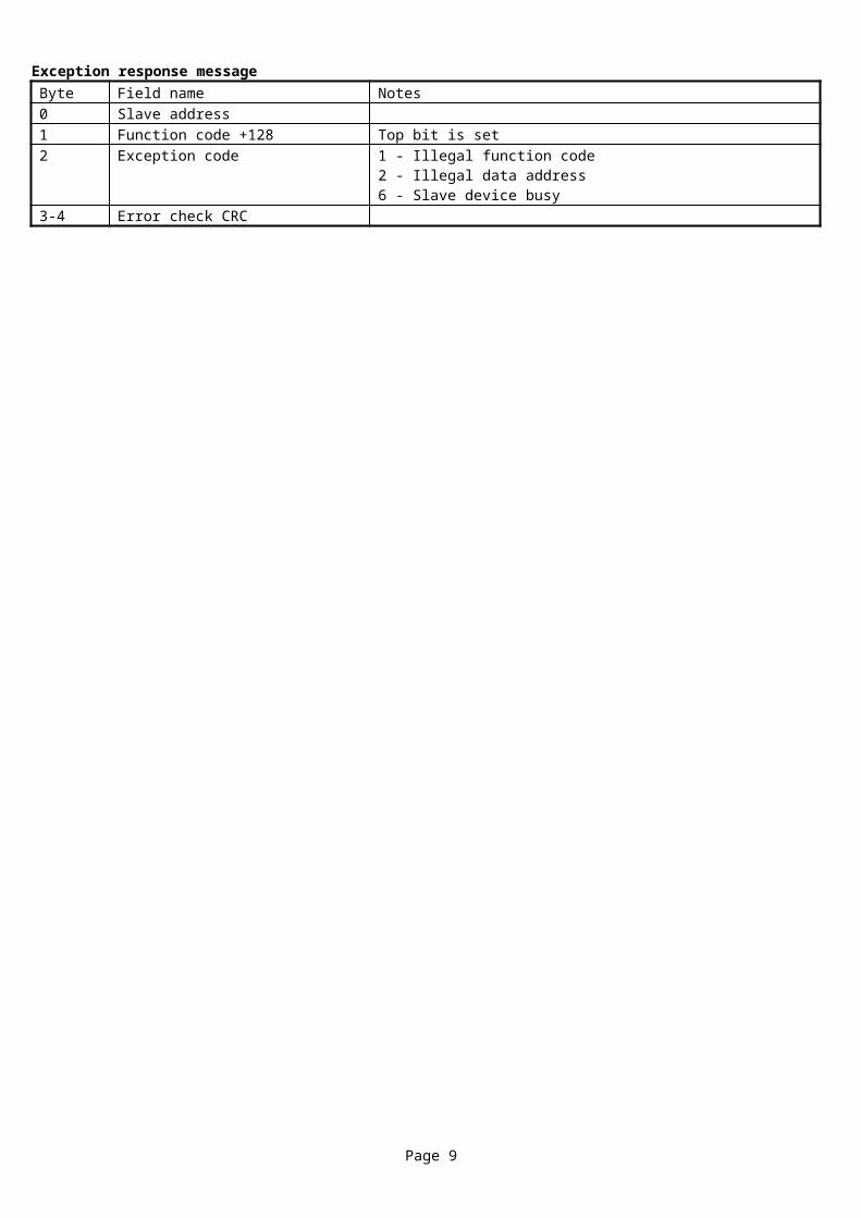
Exception response messageByte Field name Notes0 Slave address1 Function code +128 Top bit is set2 Exception code 1 - Illegal function code
2 - Illegal data address6 - Slave device busy
3-4 Error check CRC
Page 6
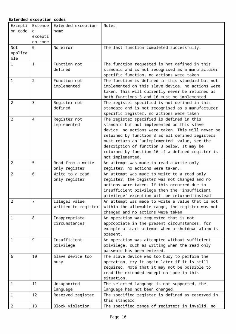
Extended exception codesException code
Extended exception code
Extended exception name Notes
Not applicable
0 No error The last function completed successfully.
1 1 Function not defined The function requested is not defined in this standard and is not recognised as a manufacturer specific function, no actions were taken
1 2 Function not implemented The function is defined in this standard but not implemented on this slave device, no actions were taken. This will currently never be returned as both functions 3 and 16 must be implemented.
2 3 Register not defined The register specified is not defined in this standard and is not recognised as a manufacturer specific register, no actions were taken
2 4 Register not implemented The register specified is defined in this standard but not implemented on this slave device, no actions were taken. This will never be returned by function 3 as all defined registers must return an ‘unimplemented’ value, see the description of function 3 below. It may be returned by function 16 if a defined register is not implemented.
2 5 Read from a write only register
An attempt was made to read a write only register, no actions were taken..
2 6 Write to a read only register An attempt was made to write to a read only register, the register was not changed and no actions were taken. If this occurred due to insufficient privilege then the ‘insufficient privilege’ exception will be returned instead
2 7 Illegal value written to register
An attempt was made to write a value that is not within the allowable range, the register was not changed and no actions were taken
1 8 Inappropriate circumstances An operation was requested that is not appropriate in the present circumstances, for example a start attempt when a shutdown alarm is present.
1 9 Insufficient privilege An operation was attempted without sufficient privilege, such as writing when the read only password has been entered.
6 10 Slave device too busy The slave device was too busy to perform the operation, try it again later if it is still required. Note that it may not be possible to read the extended exception code in this situation.
1 11 Unsupported language The selected language is not supported, the language has not been changed.
1 12 Reserved register The specified register is defined as reserved in this standard2 13 Block violation The specified range of registers in invalid, no actions were taken. An
attempt to read part of a state string would cause this error for example.14-255 Reserved Reserved for future use in this standard
1 256 No satellite socket Returned by a hub only. The specified satellite state is ‘No socket’.1 257 Satellite disabled Returned by a hub only. The specified satellite state is ‘Disabled’.1 258 Satellite error Returned by a hub only. The specified satellite state is ‘Error’.
259-32767
Reserved Reserved for future use in this standard
1/2 32767-65535
Manufacturer specific error An error occurred in a manufacturer specific operation either using register pages 128-255 or functions other than 3 and 16. The meaning of these exception codes is manufacturer specific, any software not knowing the meaning for a particular slave must print the message ‘Manufacturer specific error n’ where n is the exception code.
Page 7
7. Modbus Functions Used This standard only uses Modbus functions 3 and 16 as recommended in the Open Modbus/TCP Specification draft 2.
Notes:1. Any other functions may be implemented if required, for example for configuration of the slave device, but are not defined in this
standard.2. Any device which requires other functions to be implemented in order to perform a task which can be performed by function 3 or 16
is deemed to be non-compliant with this standard.
Functions usedFunction number
Function name Defined by Modicon
Notes
03 Read multiple registers Yes Reads one or more registers.16 Write multiple registers Yes Writes one or more registers.
8. Description of Each Function 8.1 Function 3 - Read Multiple Registers Reads one or more 16 bit registers from the slave device.
Notes:1. The limit of 125 registers is to comply with the Modbus specification which requires that a message must not exceed 256 bytes
including all fields.2. Any request for a register that is defined in this standard must return a normal response, if the register is not implemented by a
particular product it must return the unimplemented value from the table below to indicate this fact, it must not return an exception.3. A request for a register that is defined in this standard as contain some unimplemented bits must return a normal response, the
unimplemented bits will contain the unimplemented value from the table below.4. A request for a register that is defined in this standard as unimplemented will return the unimplemented value from the table below.5. A request for a register that is defined as reserved in this standard will return extended exception code 12 (Reserved register).6. A read from a multi-register value such as a 32 bit value or a string must be performed by a single message, not by multiple ones.
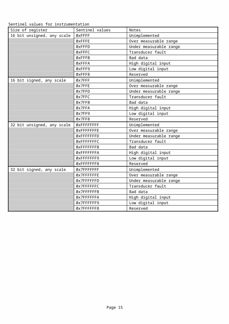
This avoids the possibility of a value being partly current and partly old data.7. The instrumentation values can return the sentinel values described in the table below to indicate a value that is over or under the
measurable range, that a transducer is faulty, that the data is bad for some other reason or that the transducer is actually a digital type.8. The sentinel value ‘high digital input’ means that the instrumentation value is high (high oil pressure, high temp, etc), similarly 'Low
digital input' means the instrumentation value is low. They do not refer to voltage levels on the inputs.
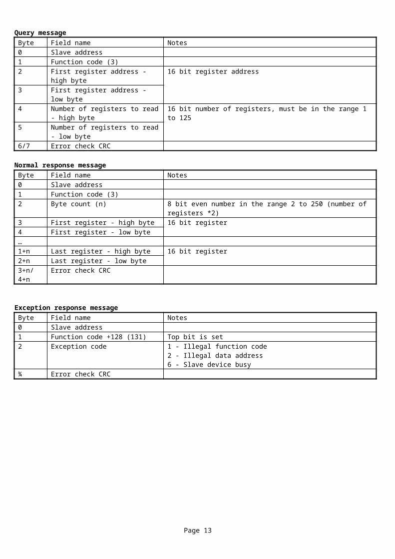
Query messageByte Field name Notes0 Slave address1 Function code (3)2 First register address - high byte 16 bit register address3 First register address - low byte4 Number of registers to read - high byte 16 bit number of registers, must be in the range 1 to 1255 Number of registers to read - low byte6/7 Error check CRC
Normal response messageByte Field name Notes0 Slave address1 Function code (3)2 Byte count (n) 8 bit even number in the range 2 to 250 (number of registers *2)3 First register - high byte 16 bit register4 First register - low byte…1+n Last register - high byte 16 bit register2+n Last register - low byte3+n/4+n Error check CRC
Page 8
Exception response messageByte Field name Notes0 Slave address1 Function code +128 (131) Top bit is set2 Exception code 1 - Illegal function code
2 - Illegal data address6 - Slave device busy
¾ Error check CRC
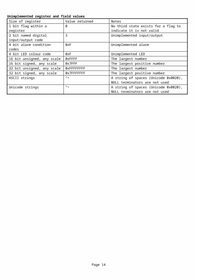
Unimplemented register and field valuesSize of register Value returned Notes1 bit flag within a register 0 No third state exists for a flag to indicate it is not valid2 bit named digital input/output code 3 Unimplemented input/output4 bit alarm condition codes 0xF Unimplemented alarm4 bit LED colour code 0xF Unimplemented LED16 bit unsigned, any scale 0xFFFF The largest number16 bit signed, any scale 0x7FFF The largest positive number32 bit unsigned, any scale 0xFFFFFFFF The largest number32 bit signed, any scale 0x7FFFFFFF The largest positive numberASCII strings “ ” A string of spaces (Unicode 0x0020), NULL
terminators are not usedUnicode strings “ ” A string of spaces (Unicode 0x0020), NULL
terminators are not used
Sentinel values for instrumentationSize of register Sentinel values Notes16 bit unsigned, any scale 0xFFFF Unimplemented
0xFFFE Over measurable range0xFFFD Under measurable range0xFFFC Transducer fault0xFFFB Bad data0xFFFA High digital input0xFFF9 Low digital input0xFFF8 Reserved
16 bit signed, any scale 0x7FFF Unimplemented0x7FFE Over measurable range0x7FFD Under measurable range0x7FFC Transducer fault0x7FFB Bad data0x7FFA High digital input0x7FF9 Low digital input0x7FF8 Reserved
32 bit unsigned, any scale 0xFFFFFFFF Unimplemented0xFFFFFFFE Over measurable range0xFFFFFFFD Under measurable range0xFFFFFFFC Transducer fault0xFFFFFFFB Bad data0xFFFFFFFA High digital input0xFFFFFFF9 Low digital input0xFFFFFFF8 Reserved
32 bit signed, any scale 0x7FFFFFFF Unimplemented0x7FFFFFFE Over measurable range0x7FFFFFFD Under measurable range0x7FFFFFFC Transducer fault0x7FFFFFFB Bad data0x7FFFFFFA High digital input0x7FFFFFF9 Low digital input0x7FFFFFF8 Reserved
Page 9
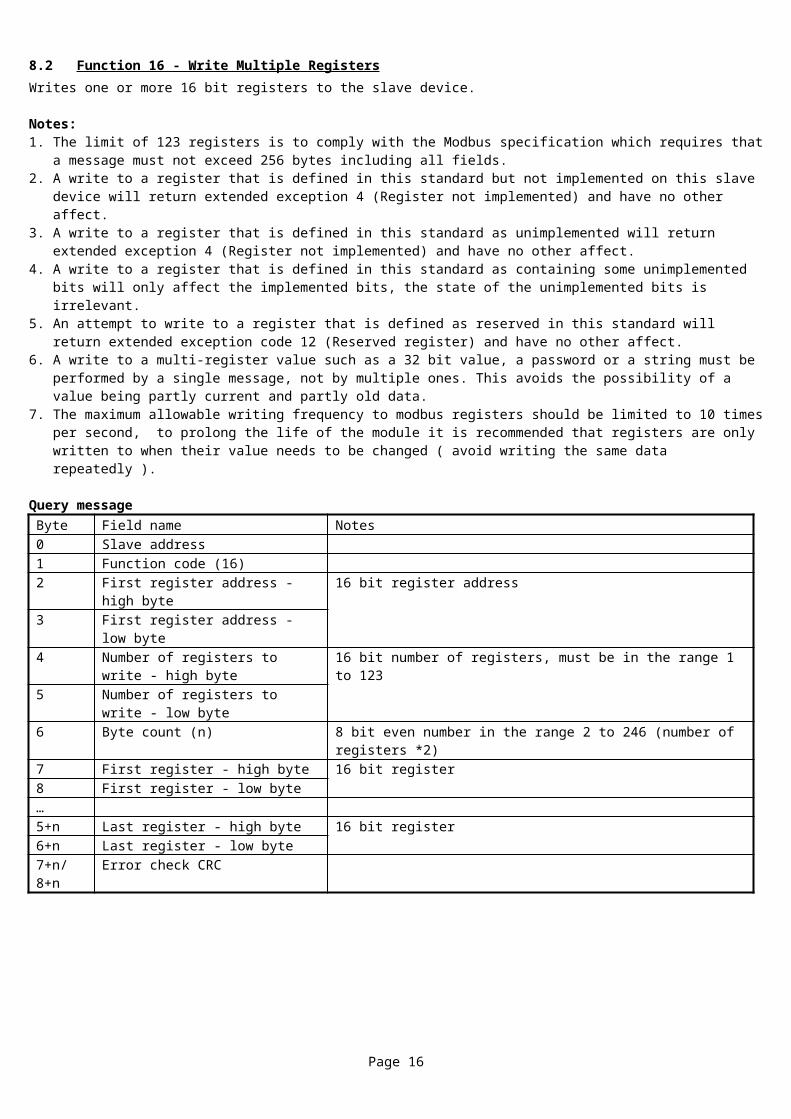
8.2 Function 16 - Write Multiple Registers Writes one or more 16 bit registers to the slave device.
Notes:1. The limit of 123 registers is to comply with the Modbus specification which requires that a message must not exceed 256 bytes
including all fields.2. A write to a register that is defined in this standard but not implemented on this slave device will return extended exception 4
(Register not implemented) and have no other affect.3. A write to a register that is defined in this standard as unimplemented will return extended exception 4 (Register not implemented)
and have no other affect.4. A write to a register that is defined in this standard as containing some unimplemented bits will only affect the implemented bits, the
state of the unimplemented bits is irrelevant.5. An attempt to write to a register that is defined as reserved in this standard will return extended exception code 12 (Reserved
register) and have no other affect.6. A write to a multi-register value such as a 32 bit value, a password or a string must be performed by a single message, not by
multiple ones. This avoids the possibility of a value being partly current and partly old data.7. The maximum allowable writing frequency to modbus registers should be limited to 10 times per second, to prolong the life of the
module it is recommended that registers are only written to when their value needs to be changed ( avoid writing the same data repeatedly ).
Query messageByte Field name Notes0 Slave address1 Function code (16)2 First register address - high byte 16 bit register address3 First register address - low byte4 Number of registers to write - high byte 16 bit number of registers, must be in the range 1 to 1235 Number of registers to write - low byte6 Byte count (n) 8 bit even number in the range 2 to 246 (number of registers *2)7 First register - high byte 16 bit register8 First register - low byte…5+n Last register - high byte 16 bit register6+n Last register - low byte7+n/8+n Error check CRC
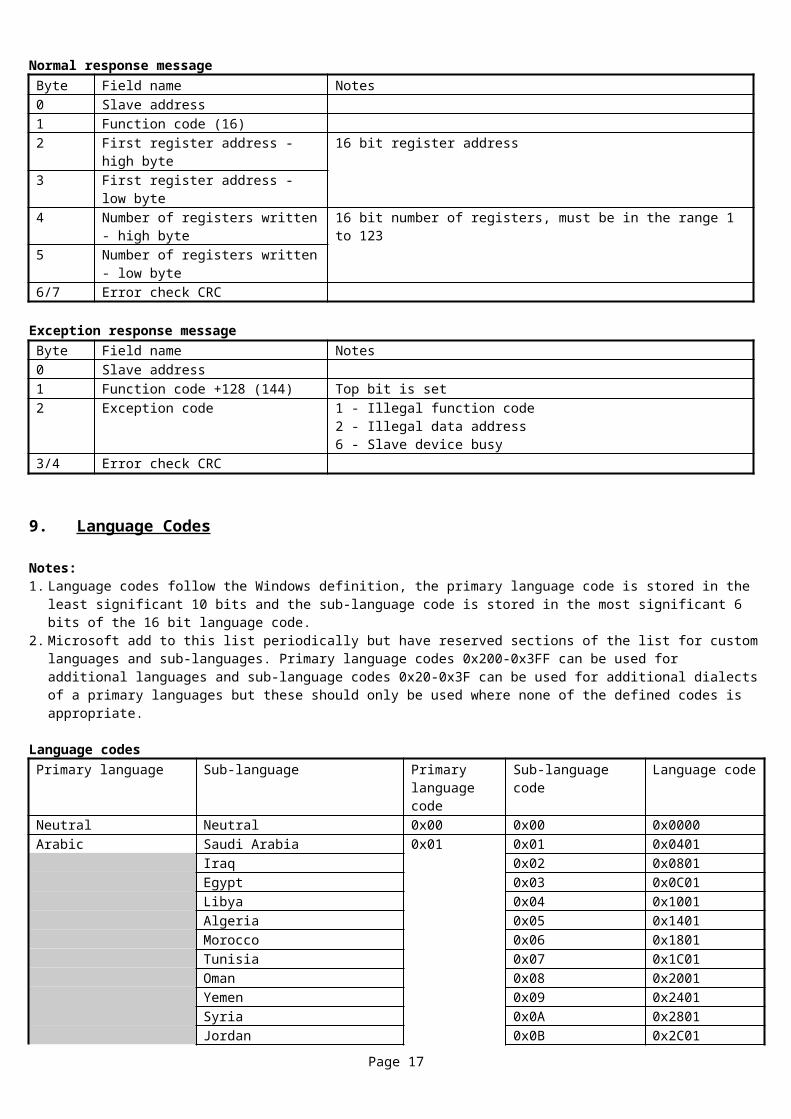
Normal response messageByte Field name Notes0 Slave address1 Function code (16)2 First register address - high byte 16 bit register address3 First register address - low byte4 Number of registers written - high byte 16 bit number of registers, must be in the range 1 to 1235 Number of registers written - low byte6/7 Error check CRC
Exception response messageByte Field name Notes0 Slave address1 Function code +128 (144) Top bit is set2 Exception code 1 - Illegal function code
2 - Illegal data address6 - Slave device busy
3/4 Error check CRC
Page 10
9. Language Codes
Notes:1. Language codes follow the Windows definition, the primary language code is stored in the least significant 10 bits and the sub-
language code is stored in the most significant 6 bits of the 16 bit language code.2. Microsoft add to this list periodically but have reserved sections of the list for custom languages and sub-languages. Primary language
codes 0x200-0x3FF can be used for additional languages and sub-language codes 0x20-0x3F can be used for additional dialects of a primary languages but these should only be used where none of the defined codes is appropriate.
Language codesPrimary language Sub-language Primary
language codeSub-language code Language code
Neutral Neutral 0x00 0x00 0x0000Arabic Saudi Arabia 0x01 0x01 0x0401
Iraq 0x02 0x0801Egypt 0x03 0x0C01Libya 0x04 0x1001Algeria 0x05 0x1401Morocco 0x06 0x1801Tunisia 0x07 0x1C01Oman 0x08 0x2001Yemen 0x09 0x2401Syria 0x0A 0x2801Jordan 0x0B 0x2C01Lebanon 0x0C 0x3001Kuwait 0x0E 0x3401United Arab Emerates 0x0E 0x3801Bahrain 0x0F 0x3C01Qatar 0x10 0x4001
Bulgarian Standard 0x02 0x01 0x0402Catalan Standard 0x03 0x01 0x0403Chinese Taiwan 0x04 0x01 0x0404
Peoples Republic 0x02 0x0804Hong Kong 0x03 0x0C04Singapore 0x04 0x1004Macau 0x05 0x1405
Czech Standard 0x05 0x01 0x0405Danish Standard 0x06 0x01 0x0406German Standard 0x07 0x01 0x0407
Swiss 0x02 0x0807Austrian 0x03 0x0C07Luxembourg 0x04 0x1007Liechtenstein 0x05 0x1407
Greek Standard 0x08 0x01 0x0408
Page 11
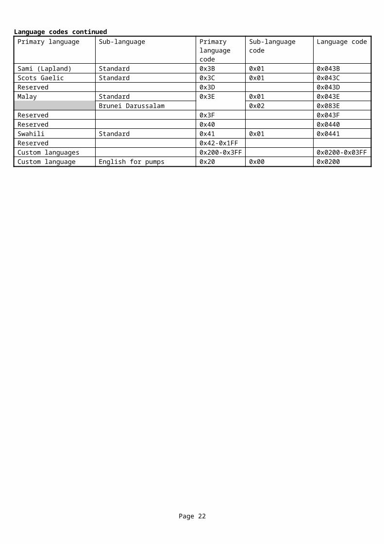
Language codes continuedPrimary language Sub-language Primary
language codeSub-language code Language code
English United states 0x09 0x01 0x0409United kingdom 0x02 0x0809Australia 0x03 0x0C09Canada 0x04 0x1009New Zealand 0x05 0x1409Ireland 0x06 0x1809South Africa 0x07 0x1C09Jamaica 0x08 0x2009Caribbean 0x09 0x2409Belize 0x0A 0x2809Trinidad 0x0B 0x2C09Zimbabwe 0x0C 0x3009Philippines 0x0D 0x3409
Spanish Traditional 0x0A 0x01 0x040AMexican 0x02 0x080AModern 0x03 0x0C0AGuatemala 0x04 0x100ACosta Rica 0x05 0x140APanama 0x06 0x180ADominican Republic 0x07 0x1C0AVenezuela 0x08 0x200AColombia 0x09 0x240APeru 0x0A 0x280AArgentina 0x0B 0x2C0AEcuador 0x0C 0x300AChile 0x0D 0x340AUruguay 0x0E 0x380AParaguay 0x0F 0x3C0ABolivia 0x10 0x400AEl Salvador 0x11 0x440AHonduras 0x12 0x480ANicaragua 0x13 0x4C0APuerto Rico 0x14 0x500A
Finnish Standard 0x0B 0x01 0x040BFrench Standard 0x0C 0x01 0x040C
Belgian 0x02 0x080CCanadian 0x03 0x0C0CSwiss 0x04 0x100CLuxembourg 0x05 0x140CMonaco 0x06 0x180C
Hebrew Standard 0x0D 0x01 0x040DHungarian Standard 0x0E 0x01 0x040EIcelandic Standard 0x0F 0x01 0x040FItalian Standard 0x10 0x01 0x0410
Swiss 0x02 0x0810Japanese Standard 0x11 0x01 0x0411Korean Extended Wansung 0x12 0x01 0x0412
Johab 0x02 0x0812Dutch Standard 0x13 0x01 0x0413
Belgian 0x02 0x0813Norwegian Bokmal 0x14 0x01 0x0414
Nynorsk 0x02 0x0814
Page 12
Language codes continuedPrimary language Sub-language Primary
language codeSub-language code Language code
Polish Standard 0x15 0x01 0x0415Portuguese Brazilian 0x16 0x01 0x0416
Standard 0x02 0x0816Rhaeto-romanic Standard 0x17 0x01 0x0417Romanian Standard 0x18 0x01 0x0418
Moldavia 0x02 0x0818Russian Standard 0x19 0x01 0x0419
Moldavia 0x02 0x0819Croatian Standard 0x1A 0x01 0x041ASerbian Latin 0x1A 0x02 0x081A
Cyrillic 0x03 0x0C1ASlovak Standard 0x1B 0x01 0x041BAlbanian Standard 0x1C 0x01 0x041CSwedish Standard 0x1D 0x01 0x041D
Finland 0x02 0x081DThai Standard 0x1E 0x01 0x041ETurkish Standard 0x1F 0x01 0x041FUrdu Standard 0x20 0x01 0x0420Indonesian Standard 0x21 0x01 0x0421Ukrainian Standard 0x22 0x01 0x0422Byelorusian Standard 0x23 0x01 0x0423Slovenian Standard 0x24 0x01 0x0424Estonian Standard 0x25 0x01 0x0425Latvian Standard 0x26 0x01 0x0426Lithuanian Standard 0x27 0x01 0x0427
Classic 0x02 0x0827Reserved 0x28 0x0428Farsi Standard 0x29 0x01 0x0429Vietnamese Standard 0x2A 0x01 0x042AReserved 0x2B 0x042BReserved 0x2C 0x042CBasque Standard 0x2D 0x01 0x042DSorbian Standard 0x2E 0x01 0x042EMacedonian Standard 0x2F 0x01 0x042FSutu Standard 0x30 0x01 0x0430Tsonga Standard 0x31 0x01 0x0431Tswana Standard 0x32 0x01 0x0432Venda Standard 0x33 0x01 0x0433Xhosa Standard 0x34 0x01 0x0434Zulu Standard 0x35 0x01 0x0435Afrikaans Standard 0x36 0x01 0x0436Reserved 0x37 0x3700Faeroese Standard 0x38 0x01 0x0438Hindi Standard 0x39 0x01 0x0439Maltese Standard 0x3A 0x01 0x043A
Page 13
Language codes continuedPrimary language Sub-language Primary
language codeSub-language code Language code
Sami (Lapland) Standard 0x3B 0x01 0x043BScots Gaelic Standard 0x3C 0x01 0x043CReserved 0x3D 0x043DMalay Standard 0x3E 0x01 0x043E
Brunei Darussalam 0x02 0x083EReserved 0x3F 0x043FReserved 0x40 0x0440Swahili Standard 0x41 0x01 0x0441Reserved 0x42-0x1FFCustom languages 0x200-0x3FF 0x0200-0x03FFCustom language English for pumps 0x20 0x00 0x0200
Page 14
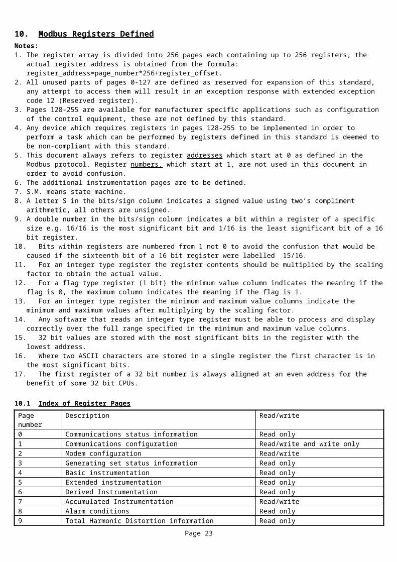
10. Modbus Registers Defined Notes:1. The register array is divided into 256 pages each containing up to 256 registers, the actual register address is obtained from the
formula: register_address=page_number*256+register_offset.2. All unused parts of pages 0-127 are defined as reserved for expansion of this standard, any attempt to access them will result in an
exception response with extended exception code 12 (Reserved register).3. Pages 128-255 are available for manufacturer specific applications such as configuration of the control equipment, these are not
defined by this standard.4. Any device which requires registers in pages 128-255 to be implemented in order to perform a task which can be performed by
registers defined in this standard is deemed to be non-compliant with this standard.5. This document always refers to register addresses which start at 0 as defined in the Modbus protocol. Register numbers, which start
at 1, are not used in this document in order to avoid confusion.6. The additional instrumentation pages are to be defined.7. S.M. means state machine.8. A letter S in the bits/sign column indicates a signed value using two’s compliment arithmetic, all others are unsigned.9. A double number in the bits/sign column indicates a bit within a register of a specific size e.g. 16/16 is the most significant bit and
1/16 is the least significant bit of a 16 bit register.10. Bits within registers are numbered from 1 not 0 to avoid the confusion that would be caused if the sixteenth bit of a 16 bit register
were labelled 15/16.11. For an integer type register the register contents should be multiplied by the scaling factor to obtain the actual value.12. For a flag type register (1 bit) the minimum value column indicates the meaning if the flag is 0, the maximum column indicates the
meaning if the flag is 1.13. For an integer type register the minimum and maximum value columns indicate the minimum and maximum values after multiplying
by the scaling factor.14. Any software that reads an integer type register must be able to process and display correctly over the full range specified in the
minimum and maximum value columns.15. 32 bit values are stored with the most significant bits in the register with the lowest address.16. Where two ASCII characters are stored in a single register the first character is in the most significant bits.17. The first register of a 32 bit number is always aligned at an even address for the benefit of some 32 bit CPUs.
10.1 Index of Register Pages Page number Description Read/write0 Communications status information Read only1 Communications configuration Read/write and write only2 Modem configuration Read/write3 Generating set status information Read only4 Basic instrumentation Read only5 Extended instrumentation Read only6 Derived Instrumentation Read only7 Accumulated Instrumentation Read/write8 Alarm conditions Read only9 Total Harmonic Distortion information Read only10 Reserved11 Diagnostic - general Read only12 Diagnostic - digital inputs Read only13 Diagnostic - digital outputs Read only and read write14 Diagnostic - LEDs Read only and read write15 Diagnostic - Reserved16 Control registers Read only and write only17 J1939 active diagnostic trouble codes in decoded format Read only18 J1939 active diagnostic trouble codes in raw format Read only19 Reserved20 Various strings Read only24 Identity strings Read/write26 State machine name strings Read only28 State machine state strings Read only29-31 Reserved
Page 15
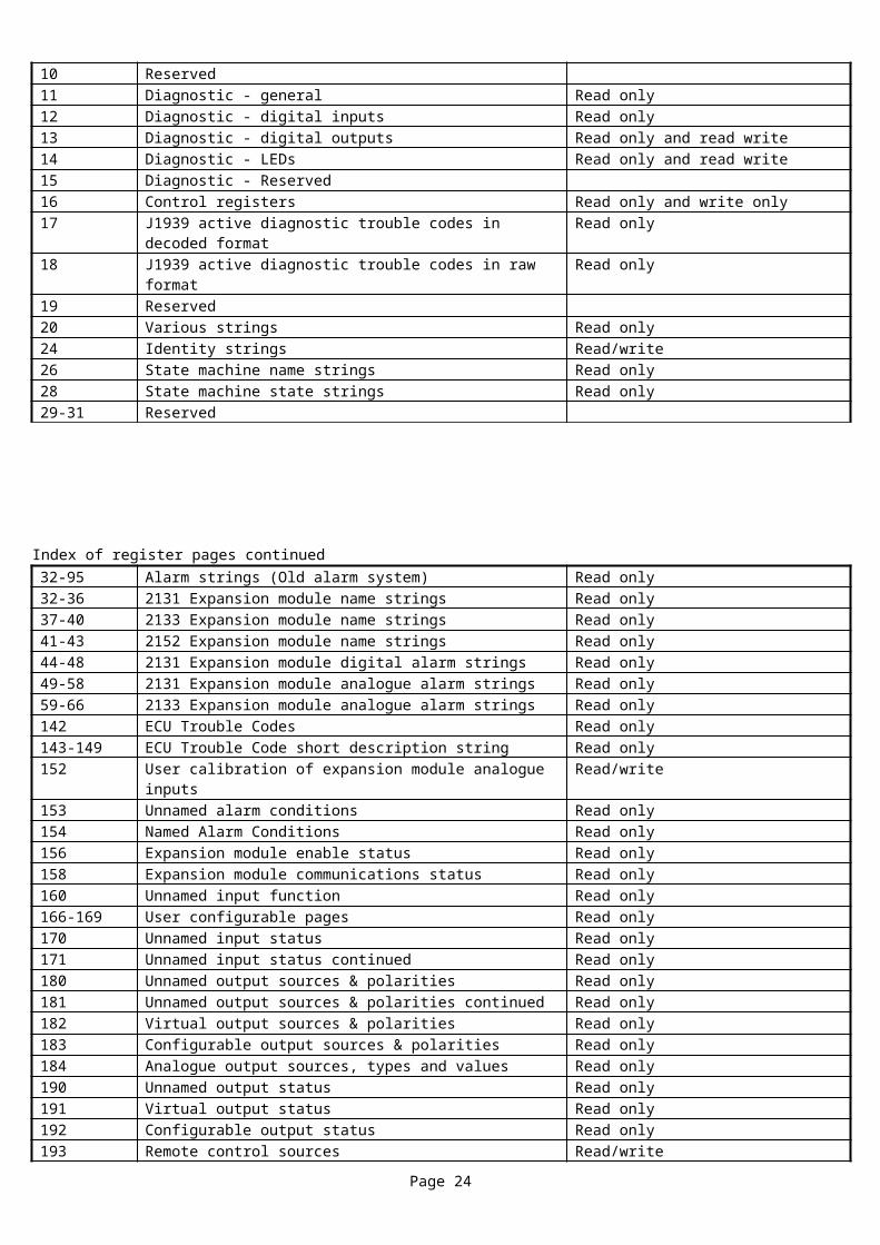
Index of register pages continued32-95 Alarm strings (Old alarm system) Read only32-36 2131 Expansion module name strings Read only37-40 2133 Expansion module name strings Read only41-43 2152 Expansion module name strings Read only44-48 2131 Expansion module digital alarm strings Read only49-58 2131 Expansion module analogue alarm strings Read only59-66 2133 Expansion module analogue alarm strings Read only142 ECU Trouble Codes Read only143-149 ECU Trouble Code short description string Read only152 User calibration of expansion module analogue inputs Read/write153 Unnamed alarm conditions Read only154 Named Alarm Conditions Read only156 Expansion module enable status Read only158 Expansion module communications status Read only160 Unnamed input function Read only166-169 User configurable pages Read only170 Unnamed input status Read only171 Unnamed input status continued Read only180 Unnamed output sources & polarities Read only181 Unnamed output sources & polarities continued Read only182 Virtual output sources & polarities Read only183 Configurable output sources & polarities Read only184 Analogue output sources, types and values Read only190 Unnamed output status Read only191 Virtual output status Read only192 Configurable output status Read only193 Remote control sources Read/write200-239 Unnamed alarm strings Read only240-246 Analogue Input Name Strings Read only250 Misc strings Read only251-255 Reserved
Page 16
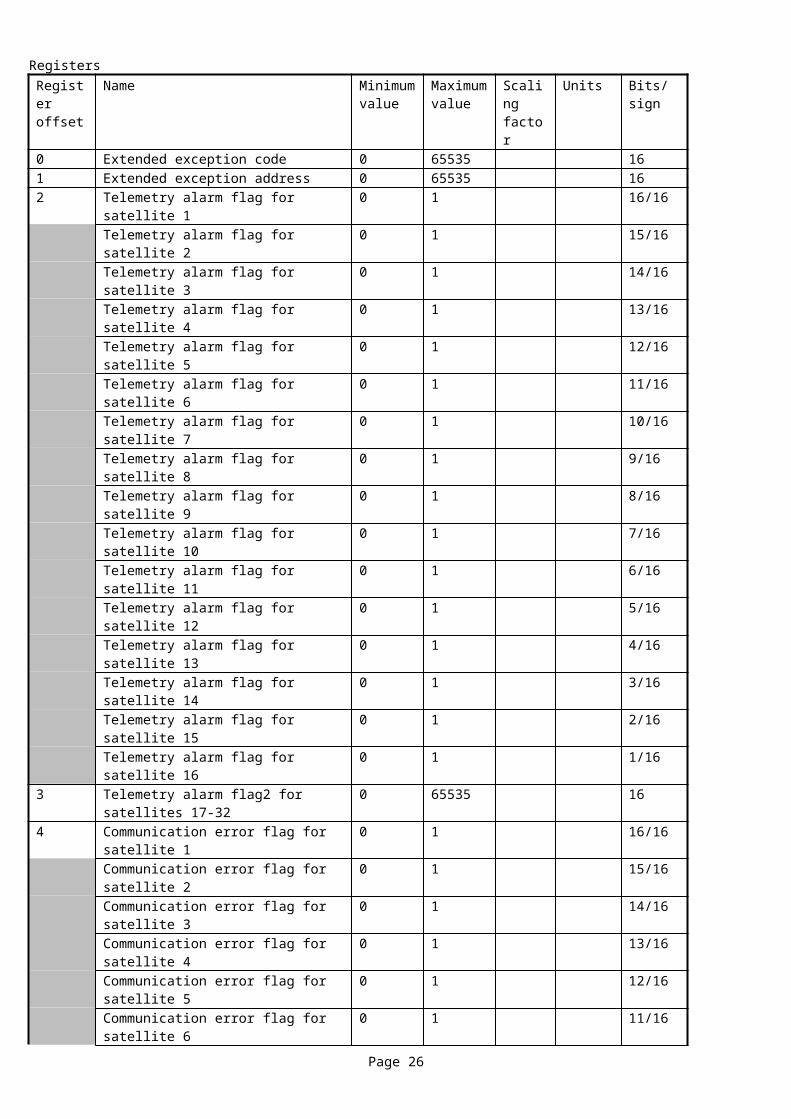
10.2 Page 0 - Communications Status Information Notes:1. These are read only registers.2. Registers 0 and 1 must both be read with a single message for them to be meaningful since they are set after each message.3. Registers 2 and 3 contain copies of the telemetry alarm flags of all satellites so that the satellite that caused a dial out can be
ascertained without reading the telemetry alarm flags from all the satellites individually. This register is not latched, clearing the telemetry alarm flag of a satellite will clear the corresponding bit in these registers when the hub updates them. The hub will not assume that sending a system control message to a satellite to clear its telemetry alarm flag will necessarily succeed, instead it builds registers 2 and 3 by reading the state of all the satellites telemetry alarm flags periodically.
4. Registers 4 and 5 contain communication error flags for all the satellites. A flag is set if, and only if, the corresponding satellite socket is fitted, it is enabled by the corresponding ‘satellite socket enable flag’ in page 1 - Communications Configuration, and the hub is not able to communicate successfully with the satellite for any reason.
5. If any communication error flag changes from 0 to 1 the hub’s telemetry alarm flag will be set and so cause a dial out if a modem is connected with dial out enabled, the satellites telemetry alarm flag in register 2 or 3 will not be set since this would contradict its non-latching operation as described in note 3 above. A system control function must be used to clear the hub’s telemetry alarm flag before the connection is broken or the dial out will be repeated.
6. The meaning of the password status is shown in the table below.7. If the password status is 0 (no valid password) then it is not possible to read the extended exception information..8. If the number of satellite sockets is 1-32 the unit is a hub, otherwise it is not. A hub with 8 sockets, for example, returns a value of 8
regardless of what is actually plugged into the sockets or what the satellites state is, and will always respond to 8 consecutive slave addresses starting with its own slave address +1.
9. The GenComm version number allows a master to recognise the version of GenComm supported by a slave device and act accordingly. 72xx/73xx modules are identified by the GenComm version of 2, 53xx/55xx etc modules have a GenComm version of 1.
10. Registers 10 and 11 contain flags that indicate the available baud rates, bit 1 corresponds to baud rate code 0 etc. If a bit is set the corresponding Baud rate is available.
11. The list of language codes that are available on a particular slave device can be obtained by first reading the number of languages available and then reading that number of registers from the beginning of the list of language codes available. Reading any further registers from the list will return the unimplemented register value 0xFFFF. The order of the language codes in the list has no significance and no assumptions should be made.
Page 17
RegistersRegister offset
Name Minimum value
Maximum value
Scaling factor
Units Bits/ sign
0 Extended exception code 0 65535 161 Extended exception address 0 65535 162 Telemetry alarm flag for satellite 1 0 1 16/16
Telemetry alarm flag for satellite 2 0 1 15/16Telemetry alarm flag for satellite 3 0 1 14/16Telemetry alarm flag for satellite 4 0 1 13/16Telemetry alarm flag for satellite 5 0 1 12/16Telemetry alarm flag for satellite 6 0 1 11/16Telemetry alarm flag for satellite 7 0 1 10/16Telemetry alarm flag for satellite 8 0 1 9/16Telemetry alarm flag for satellite 9 0 1 8/16Telemetry alarm flag for satellite 10 0 1 7/16Telemetry alarm flag for satellite 11 0 1 6/16Telemetry alarm flag for satellite 12 0 1 5/16Telemetry alarm flag for satellite 13 0 1 4/16Telemetry alarm flag for satellite 14 0 1 3/16Telemetry alarm flag for satellite 15 0 1 2/16Telemetry alarm flag for satellite 16 0 1 1/16
3 Telemetry alarm flag2 for satellites 17-32 0 65535 164 Communication error flag for satellite 1 0 1 16/16
Communication error flag for satellite 2 0 1 15/16Communication error flag for satellite 3 0 1 14/16Communication error flag for satellite 4 0 1 13/16Communication error flag for satellite 5 0 1 12/16Communication error flag for satellite 6 0 1 11/16Communication error flag for satellite 7 0 1 10/16Communication error flag for satellite 8 0 1 9/16Communication error flag for satellite 9 0 1 8/16Communication error flag for satellite 10 0 1 7/16Communication error flag for satellite 11 0 1 6/16Communication error flag for satellite 12 0 1 5/16Communication error flag for satellite 13 0 1 4/16Communication error flag for satellite 14 0 1 3/16Communication error flag for satellite 15 0 1 2/16Communication error flag for satellite 16 0 1 1/16
5 Communication error flags for satellites 17-32
0 65535 16
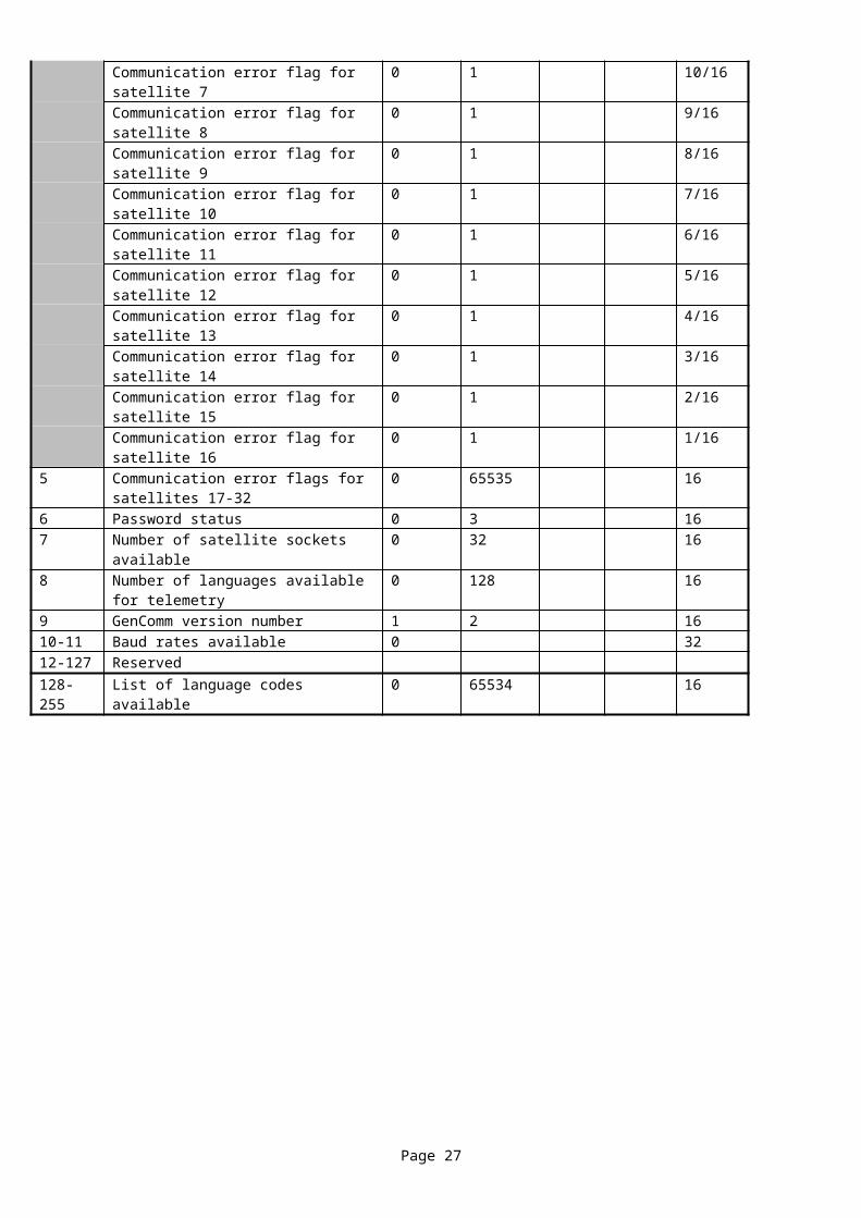
6 Password status 0 3 167 Number of satellite sockets available 0 32 168 Number of languages available for telemetry 0 128 169 GenComm version number 1 2 1610-11 Baud rates available 0 3212-127 Reserved128-255 List of language codes available 0 65534 16
Page 18
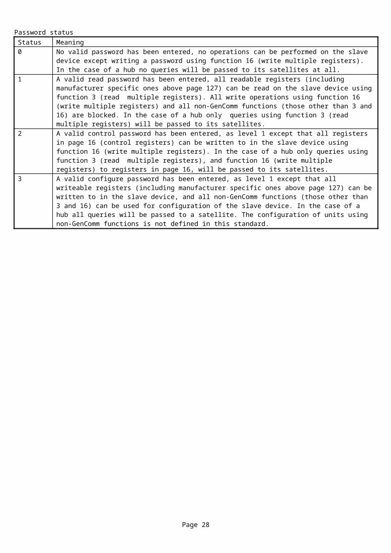
Password statusStatus Meaning0 No valid password has been entered, no operations can be performed on the slave device except writing a password
using function 16 (write multiple registers). In the case of a hub no queries will be passed to its satellites at all.1 A valid read password has been entered, all readable registers (including manufacturer specific ones above page 127)
can be read on the slave device using function 3 (read multiple registers). All write operations using function 16 (write multiple registers) and all non-GenComm functions (those other than 3 and 16) are blocked. In the case of a hub only queries using function 3 (read multiple registers) will be passed to its satellites.
2 A valid control password has been entered, as level 1 except that all registers in page 16 (control registers) can be written to in the slave device using function 16 (write multiple registers). In the case of a hub only queries using function 3 (read multiple registers), and function 16 (write multiple registers) to registers in page 16, will be passed to its satellites.
3 A valid configure password has been entered, as level 1 except that all writeable registers (including manufacturer specific ones above page 127) can be written to in the slave device, and all non-GenComm functions (those other than 3 and 16) can be used for configuration of the slave device. In the case of a hub all queries will be passed to a satellite. The configuration of units using non-GenComm functions is not defined in this standard.
Page 19
10.3 Page 1 - Communications Configuration
Notes:1. These are a mixture of read/write and write only registers (except on 72xx/73xx where registers 0-9 are read-only, not read/write).2. The current slave address is fixed at 10 in the case of an RS232 link to a modem, or direct to a PC, since there is no point in changing
a slave address on a 1 to 1 link. Address 10 was chosen so that that satellite 1 has slave address 1 etc. Register 0 specifies the current slave address in all other cases.
3. The site identity code is user definable and is used to identify a site.4. The device identity code is user definable and is used to identify a device within a site.5. The meaning of the baud rate is shown in the table below, a slave device may not necessarily support all baud rates, writing an
unsupported value will return extended exception 7 (Illegal value written to register) and will not change the Baud rate. Some systems may not allow the Baud rate to be changed at all, it may be set by switches or from a user interface for example. The baud rates available on a particular slave can be obtained by reading a register in the communications status page.
6. The current language applies only to strings read by telemetry, it is quite separate from the language selected for any user interface on the unit. The meaning of the code is defined in the language codes section.
7. The satellite socket enable flags allow each satellite socket to be enabled or disabled, a socket that is fitted but not in use must be disabled or the hub will think that the lack of response indicates a problem and set the corresponding satellite error flag and telemetry alarm flag. The enable flag for a socket that is not fitted will always be 0, any attempt to set it will be ignored.
8. The master inactivity time-out is used to detect the loss of communication from the master, if a query is not received for this period the slave device assumes the link to the master has been lost. The link is assumed to have been established as soon as a query arrives from the master.
9. The password time-out is used to disable the password automatically, if a valid password is not written for this period the password status will be set to 0 (invalid) or the highest disabled password level.
10. The display unit connected to module indicates which type of unit is connected to the 8700. A zero value indicates there is no display unit connected and the module is locked.
Notes on passwords:1. Passwords are intended to control access to control equipment via telemetry, they are not necessarily the same as passwords used to
access the same equipment from a user interface. Such user interfaces are not defined in this standard in any way.2. Passwords are 4 digit numbers similar to ‘PIN numbers’ which are widely accepted and easier to enter via a limited user interface
than alphanumeric strings.3. One of the 3 valid passwords is written into register 32 and its ones-compliment written into register 33 with a single function 16
(write multiple registers) to set the current password status. 4. The password status in the communications status information page indicates which level of access has been granted, when the
password times out the status becomes 0 (invalid) or the highest disabled password level.5. Entering a password that does not match one of the 3 valid passwords will cause the password status to be set to 0 (invalid) or the
highest disabled password level and return extended exception 7 (Illegal value written to register)6. The password status can be cleared to 0 (invalid) or the highest disabled password level either by writing a password that is known to
be invalid or by writing any value to register 32 without writing to register 33.7. If an invalid password is entered 3 times the slave device will then reject any further attempt to enter a password for a 1 minute
lockout period, returning extended exception 8 (Inappropriate circumstances) at the third attempt (so it is immediately clear what has happened) and whenever a further attempt is made to enter a password during the lockout period. The password lockout period will double after every 3 unsuccessful attempts to enter a password, up to a maximum of 64 minutes, thus minimising the risk of a deliberate attack being able to find a valid password. When a valid password is entered the count of invalid entries will be reset to 0. The count of invalid entries and the current lockout timer will not be reset by loss of the communication link as it would be possible for an attacker to drop the link to reset them and then immediately re-establish the link.
8. When the link to a master is lost (a phone line is dropped or the master inactivity timer expires for example) the password status is set to 0 (invalid) or the highest disabled password level.
9. The ‘read only’ password is changed by writing the new value to register 34 and its ones-compliment to register 35 with a single function 16 (write multiple registers), any other operation will fail to change the password and return extended exception 7 (Illegal value written to register). The ‘control’ and ‘configure’ passwords are changed in the same way using the appropriate registers. The current ‘configure’ password must have been entered before any passwords can be changed.
10. If a password is changed to 0000 then that password level will be disabled, the password status will then default to the highest level that is disabled rather than 0 when an invalid password is entered, the password times out or the link to the master is lost. Even if one or more of the passwords has been changed to 0000, any attempt to write a password of 0000 to register 32 and 33 will be treated exactly as if an invalid password was entered.
11. A hub is intended to provide security for all its satellites using its own passwords, thus avoiding the complexity of managing passwords in every satellite separately, to facilitate this each satellite must have all its passwords disabled by setting them to 0000. If this is not done it is not possible to enter any password into a satellite unless the configure password is entered into the hub first, this is necessary to simplify the message filtering mechanism needed in the hub but is not a problem if the hub is used to provide security to the satellites as intended.
Page 20
RegistersRegister offset
Name Minimum value
Maximum value
Scaling factor
Units Bits/ sign Read/write
0 Current slave address 1 247 16 Read/write1 Site identity code 0 65534 16 Read/write2 Device identity code 0 65534 16 Read/write3 Baud rate 0 12 16 Read/write4 Current language code 0 65534 16 Read/write5 Unimplemented 0xFFFF 0xFFFF 16 Read only6 Satellite socket 1 enable flag 0 1 16/16 Read/write
Satellite socket 2 enable flag 0 1 15/16 Read/writeSatellite socket 3 enable flag 0 1 14/16 Read/writeSatellite socket 4 enable flag 0 1 13/16 Read/writeSatellite socket 5 enable flag 0 1 12/16 Read/writeSatellite socket 6 enable flag 0 1 11/16 Read/writeSatellite socket 7 enable flag 0 1 10/16 Read/writeSatellite socket 8 enable flag 0 1 9/16 Read/writeSatellite socket 9 enable flag 0 1 8/16 Read/writeSatellite socket 10 enable flag 0 1 7/16 Read/writeSatellite socket 11 enable flag 0 1 6/16 Read/writeSatellite socket 12 enable flag 0 1 5/16 Read/writeSatellite socket 13 enable flag 0 1 4/16 Read/writeSatellite socket 14 enable flag 0 1 3/16 Read/writeSatellite socket 15 enable flag 0 1 2/16 Read/writeSatellite socket 16 enable flag 0 1 1/16 Read/write
7 Satellite socket 17-32 enable flags 0 65535 16 Read/write8 Master inactivity time-out, 0 means never
time-out0 36,000 0.1 Seconds 16 Read/write
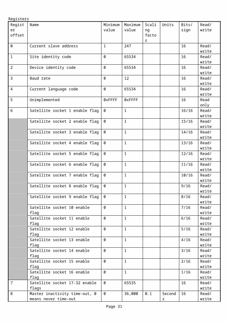
9 Password time-out, 0 means never time-out 0 36,000 0.1 Seconds 16 Read/write10-31 Reserved32 Current password 0 9999 1 16 Write only33 Compliment of current password 55536 65535 1 16 Write only34 Set new read only password 0 9999 1 16 Write only35 Compliment of new read only password 55536 65535 1 16 Write only36 Set new control password 0 9999 1 16 Write only37 Compliment of new control password 55536 65535 1 16 Write only38 Set new configure password 0 9999 1 16 Write only39 Compliment of new configure password 55536 65535 1 16 Write only40 Display unit type connected to module 0 65535 1 16 Read only41-255 Reserved
Baud rateCode Rate0 1101 1502 3003 6004 12005 24006 48007 96008 144009 1920010 2880011 3840012 5760013 11520014-99 Reserved
Page 21
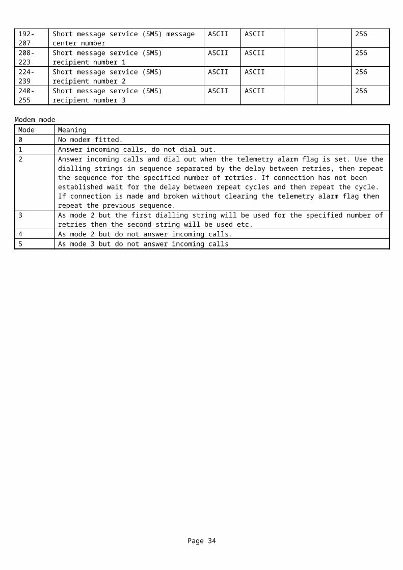
10.4 Page 2 - Modem Configuration
Notes1. These are read/write registers (except on 72xx/73xx where they are read-only & only updated by writing a configuration file).2. Modem control strings can contain any ASCII characters and are padded with spaces (ASCII 0x20), NULL terminators are not used.3. Each string is automatically suffixed with <CR><LF> so these should not be included in the string, strings are not automatically
prefixed with ‘AT’ so these must be included when required.4. A string may contain a meta character consisting of 3 tildes (~~~) which indicates that a pause of 1 second should be introduced
before the rest of the string is sent to the modem. This meta character may be repeated if longer delays are required. The tildes will not be sent to the modem.
5. If a dialling string contains only spaces (ASCII 0x20) it will not be used in the dialling sequence.6. The meaning of the modem’s mode is described in the table below.7. The modem dial back string can be used by a master to call the slave device, it is never used by the slave device..8. The SMS enable flag enables the transmission of SMS messages over a GSM modem, the method of transmission, circumstances
that trigger a transmission and contents of the messages are not defined in this standard.9. The SMS message centre number and recipient number are in the same format as the other modem control strings and are only used
when the SMS system is activated by the SMS enable flag, their use is not defined in this standard.
RegistersRegister offset
Name Minimum value
Maximum value
Scaling factor
Units Bits/ sign
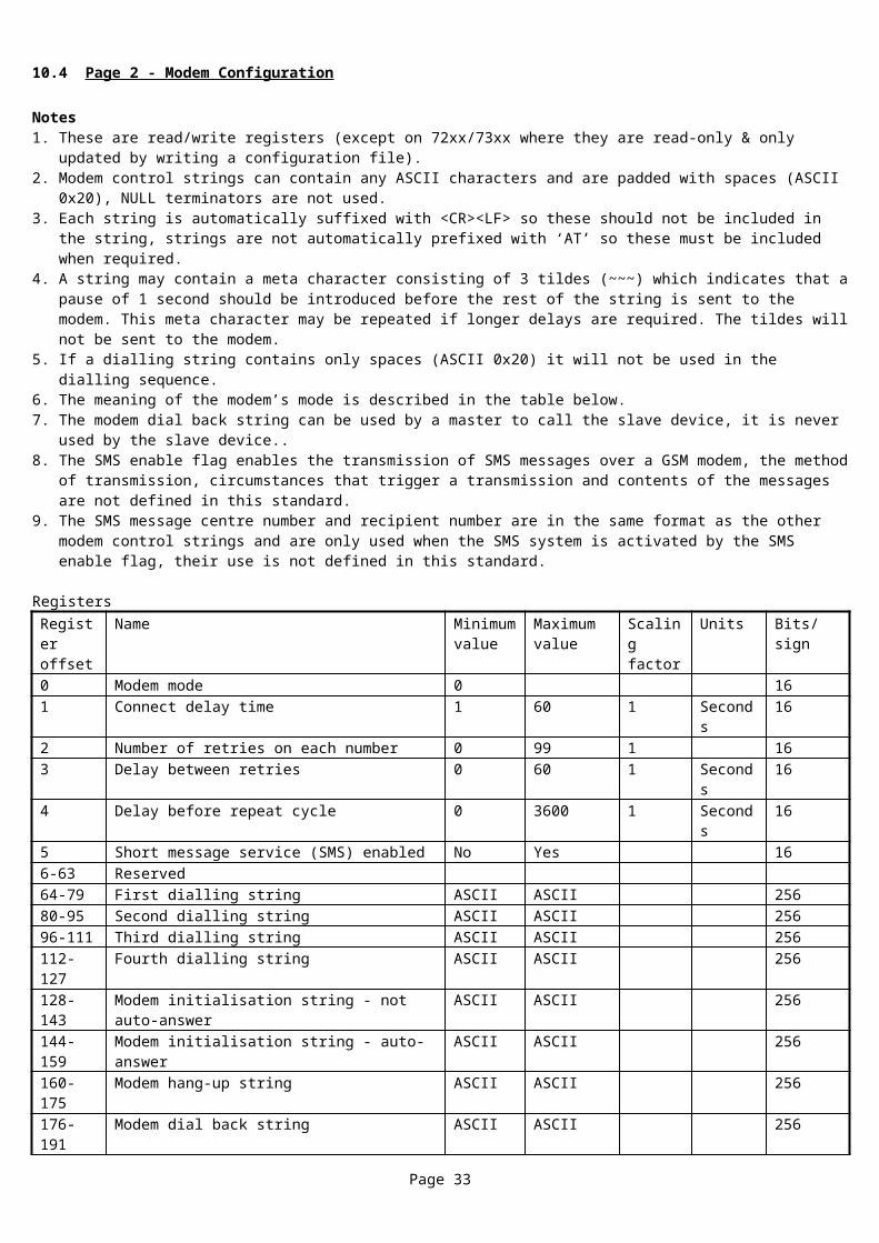
0 Modem mode 0 161 Connect delay time 1 60 1 Seconds 162 Number of retries on each number 0 99 1 163 Delay between retries 0 60 1 Seconds 164 Delay before repeat cycle 0 3600 1 Seconds 165 Short message service (SMS) enabled No Yes 166-63 Reserved64-79 First dialling string ASCII ASCII 25680-95 Second dialling string ASCII ASCII 25696-111 Third dialling string ASCII ASCII 256112-127 Fourth dialling string ASCII ASCII 256128-143 Modem initialisation string - not auto-answer ASCII ASCII 256144-159 Modem initialisation string - auto-answer ASCII ASCII 256160-175 Modem hang-up string ASCII ASCII 256176-191 Modem dial back string ASCII ASCII 256192-207 Short message service (SMS) message center number ASCII ASCII 256208-223 Short message service (SMS) recipient number 1 ASCII ASCII 256224-239 Short message service (SMS) recipient number 2 ASCII ASCII 256240-255 Short message service (SMS) recipient number 3 ASCII ASCII 256
Modem modeMode Meaning0 No modem fitted.1 Answer incoming calls, do not dial out.2 Answer incoming calls and dial out when the telemetry alarm flag is set. Use the dialling strings in sequence separated
by the delay between retries, then repeat the sequence for the specified number of retries. If connection has not been established wait for the delay between repeat cycles and then repeat the cycle. If connection is made and broken without clearing the telemetry alarm flag then repeat the previous sequence.
3 As mode 2 but the first dialling string will be used for the specified number of retries then the second string will be used etc.
4 As mode 2 but do not answer incoming calls.5 As mode 3 but do not answer incoming calls
Page 22
10.5 Page 3 - Generating Set Status Information Notes:1. These are read only registers.2. A unique manufacturer code is assigned to each manufacturer.3. The meaning of the model number is manufacturer specific, e.g. two manufacturers may have a model 100.4. The manufacturer code and model number must be used together to identify a particular product unambiguously.5. The meaning of the control mode is shown in the table below.6. The shutdown flag on a control unit indicates that one or more of the alarm codes has been set to ‘shutdown alarm’, it will clear
automatically when no alarm codes are set to shutdown alarm. A system control function is used to clear shutdown alarms. In some situations it may not be possible to set one of the alarm codes to indicate the type of shutdown alarm because the type is not known, in this case only the shutdown flag will be set and the master should consider it an undefined shutdown alarm.
7. The shutdown alarm flag on a hub indicate that state of the hub itself, not the state of any satellite. The state of a satellite must be read from the satellite itself.
8. The electrical trip and warning alarm flags operate in the same way as the shutdown alarm flag but for the corresponding alarm codes.
9. The telemetry alarm flag on a control unit is set when the control unit decides that a dial-out is required, the logic behind this is product specific. It can only be cleared by a system control function.
10. The telemetry alarm flag on a hub is only set if the hub itself has a problem, and can only be cleared by a system control function. It is edge triggered i.e. once it is cleared it will not be set unless the internal error is cleared and then happens again. An example of a situation that will set this flag is if the hub loses communication with a satellite.
11. The satellite telemetry alarm flag is the OR of all the satellite telemetry alarm flags in the ‘telemetry status and configuration’ page and indicates that one or more satellites requires servicing.
12. Whenever the telemetry alarm flag (or one of the satellite telemetry alarm flags in the case of a hub) is set it will cause continual dial outs if a modem is fitted and dial out is enabled.
13. The meaning of the state machine status is described in the table below.14. The string checksum is the sum of every character in every fixed string in the slave device, it is used to detect the substitution of a
slave device that differs only in its strings and thus check the validity of any copies of these strings held by a master. This number must not change during the normal operation of the slave device. The exact method of calculating the checksum must not be assumed and it must not be compared with a checksum generated my a master, it must only be compared with a previously read checksum to determine change.
15. The state machine state (registers 18-25) indicate the current state of each state machine, the conversion between state code and string is specific to each model and not covered in this document, refer to DSE for documentation.
Page 23
RegistersRegister offset
Name Minimum value
Maximum value
Scaling factor
Units Bits/ sign
0 Manufacturer code 0 65534 1 161 Model number 0 65534 1 162-3 Serial number 0 999999999 1 324 Control mode 0 65535 1 165 Control mode selection
(330/331/334/335)0 65535 1 16
6 Control unit not configured No Yes 16/16Unimplemented 0 0 15/16Control unit failure No Yes 14/16Shutdown alarm active No Yes 13/16Electrical trip alarm active No Yes 12/16Warning alarm active No Yes 11/16Telemetry alarm flag Not active Active 10/16Satellite telemetry alarm flag Not active Active 9/16No font file No Yes 8/16Unimplemented 0 0 1/16-7/16
7 S.M. 1 status 0 3 16/16-15/16S.M. 2 status 0 3 14/16-13/16S.M. 3 status 0 3 12/16-11/16S.M. 4 status 0 3 10/16-9/16S.M. 5 status 0 3 8/16-7/16S.M. 6 status 0 3 6/16-5/16S.M. 7 status 0 3 4/16-3/16S.M. 8 status 0 3 2/16-1/16
8-9 String checksum 0 0xFFFFFFFF 3210 S.M. 1 timer 0 65534 1 Seconds 1611 S.M. 2 timer 0 65534 1 Seconds 1612 S.M. 3 timer 0 65534 1 Seconds 1613 S.M. 4 timer 0 65534 1 Seconds 1614 S.M. 5 timer 0 65534 1 Seconds 1615 S.M. 6 timer 0 65534 1 Seconds 1616 S.M. 7 timer 0 65534 1 Seconds 1617 S.M. 8 timer 0 65534 1 Seconds 1618 S.M. 1 state 0 65535 1 1619 S.M. 2 state 0 65535 1 1620 S.M. 3 state 0 65535 1 1621 S.M. 4 state 0 65535 1 1622 S.M. 5 state 0 65535 1 1623 S.M. 6 state 0 65535 1 1624 S.M. 7 state 0 65535 1 1625 S.M. 8 state 0 65535 1 1626 Change in event log contents No Yes27-255 Reserved
Page 24
Control modesMode Description0 Stop mode1 Auto mode2 Manual mode3 Test on load mode4 Auto with manual restore mode/Prohibit Return5 User configuration mode6 Test off load mode7-65534 Reserved65535 Unimplemented
Notes on control modes:1. ‘Stop mode’ means stop the engine (generator) and in the case of ‘automatic mains failure units’ transfer the load to the mains if
possible.2. ‘Auto mode’ means automatically start the engine (generator) in the event of a remote start signal or a mains-failure, and in the case
of ‘automatic mains failure units’ transfer the load to the generator when available. When the remote start signal is removed or the mains returns, stop the engine (generator) and in the case of ‘automatic mains failure units’ transfer the load back to the mains.
3. ‘Manual mode’ means start the engine (generator) With some control units it will also be necessary to press the start button before such a manual start is initiated. In the case of ‘automatic mains failure units’ do not transfer the load to the generator unless the mains fails.
4. ‘Test on load mode’ means start the engine (generator) With some control units it will also be necessary to press the start button before such a manual start is initiated. Transfer the load to the generator when it is available, regardless of the mains condition. This mode is only provided on automatic mains failure units.
5. ‘Auto with manual restore mode’ means the same as 2 above but when the remote start signal is removed or the mains returns, the engine (generator) will not stop and the load will not be transferred back to the mains. This mode is only provided on automatic mains failure units.
6. ‘User configuration mode’ means that the unit is being configured from its user interface and is not available for normal operation, there is no method of entering or leaving this mode by telemetry, it must be done from the user interface.
7. Any control unit that does not have a control mode will return the unimplemented value.8. Register 5 is used to select control modes for use with SCADA mimic screens on modules that have a single mode button (currently
330/331/334/335) in conjunction with page 16. System control code 35714 causes this value to scroll though the available control mode values. System control code 35715 causes the selected control mode to be applied. If neither of these two control modes are received for a period of two minutes then the value will revert to the value stored in register 4.
9. ‘Test off load mode’ means start the engine (generator/S2). The load will not be transferred to S2.
State machine statusStatus Description0 Implemented but not changed since last read of state string1 Implemented and changed since last read of state string2 Reserved3 Unimplemented
Notes on state machine status:1. A state machine that is implemented (status 0 or 1) has a fixed name string in page 27 that can be used in a status display, the name
strings for unimplemented state machines will contain 32 spaces (Unicode 0x0020).2. A state machine that is implemented has a state string in page 28 which may be used in a status display. The contents of this string
will change when the state machine changes state and this is indicated by the status changing from 0 to 1, when the state string is read the status will change back from 1 to 0. This means that the string only has to be read when there is a change in state, thus minimising the volume of traffic.
State machine statesState Description0-65534 Reserved65535 Unimplemented
Page 25
10.6 Page 4 - Basic Instrumentation Notes:1. These are read only registers.2. The meaning of the mains, generator and bus phase rotation codes is given in the table below.3. Registers 95-123 have been added to support the 8680 although not all will be implemented initially.4. Registers 180 to 192 added to allow mimics of either S1 or S2 load/watts/lead-lag registers according to which side is on load.
Register offset
Name Minimum value
Maximum value
Scaling factor
Units Bits/ sign
0 Oil pressure 0 10000 1 KPa 161 Coolant temperature -50 200 1 Degrees C 16 S2 Oil temperature -50 200 1 Degrees C 16 S3 Fuel level 0 130 1 % 164 Charge alternator voltage 0 40 0.1 V 165 Battery voltage 0 40 0.1 V 166 Engine speed 0 6000 1 RPM 167 Generator frequency 0 70 0.1 Hz 168-9 Generator L1-N voltage 0 18,000 0.1 V 3210-11 Generator L2-N voltage 0 18,000 0.1 V 3212-13 Generator L3-N voltage 0 18,000 0.1 V 3214-15 Generator L1-L2 voltage 0 30,000 0.1 V 3216-17 Generator L2-L3 voltage 0 30,000 0.1 V 3218-19 Generator L3-L1 voltage 0 30,000 0.1 V 3220-21 Generator L1 current 0 99,999.9 0.1 A 3222-23 Generator L2 current 0 99,999.9 0.1 A 3224-25 Generator L3 current 0 99,999.9 0.1 A 3226-27 Generator earth current 0 99,999.9 0.1 A 3228-29 Generator L1 watts -99,999,999 99,999,999 1 W 32 S30-31 Generator L2 watts -99,999,999 99,999,999 1 W 32 S32-33 Generator L3 watts -99,999,999 99,999,999 1 W 32 S34 Generator current lag/lead -180 +180 1 degrees 16 S35 Mains frequency 0 70 0.1 Hz 1636-37 Mains L1-N voltage 0 18,000 0.1 V 3238-39 Mains L2-N voltage 0 18,000 0.1 V 3240-41 Mains L3-N voltage 0 18,000 0.1 V 3242-43 Mains L1-L2 voltage 0 30,000 0.1 V 3244-45 Mains L2-L3 voltage 0 30,000 0.1 V 3246-47 Mains L3-L1 voltage 0 30,000 0.1 V 3248 Mains voltage phase lag/lead -180 +180 1 degrees 16 S49 Generator phase rotation 0 3 1650 Mains phase rotation 0 3 1651 Mains current lag/lead -180 +180 1 degrees 16 S52-53 Mains L1 current 0 99,999.9 0.1 A 3254-55 Mains L2 current 0 99,999.9 0.1 A 3256-57 Mains L3 current 0 99,999.9 0.1 A 3258-59 Mains earth current 0 99,999.9 0.1 A 3260-61 Mains L1 watts -99,999,999 99,999,999 1 W 32 S62-63 Mains L2 watts -99,999,999 99,999,999 1 W 32 S64-65 Mains L3 watts -99,999,999 99,999,999 1 W 32 S66 Bus current lag/lead -180 +180 1 degrees 16 S67 Bus frequency 0 70 0.1 Hz 1668-69 Bus L1-N voltage 0 18,000 0.1 V 3270-71 Bus L2-N voltage 0 18,000 0.1 V 3272-73 Bus L3-N voltage 0 18,000 0.1 V 3274-75 Bus L1-L2 voltage 0 30,000 0.1 V 3276-77 Bus L2-L3 voltage 0 30,000 0.1 V 3278-79 Bus L3-L1 voltage 0 30,000 0.1 V 32
Page 26
Basic instrumentation continued
Page 27
Register offset
Name Minimum value
Maximum value
Scaling factor
Units Bits/ sign
80-81 Bus L1 current 0 99,999.9 0.1 A 3282-83 Bus L2 current 0 99,999.9 0.1 A 3284-85 Bus L3 current 0 99,999.9 0.1 A 3286-87 Bus earth current 0 99,999.9 0.1 A 3288-89 Bus L1 watts -999,999,999 999,999,999 1 W 32 S90-91 Bus L2 watts -999,999,999 999,999,999 1 W 32 S92-93 Bus L3 watts -999,999,999 999,999,999 1 W 32 S94 Bus phase rotation 0 3 1695 Bus 2 frequency 0 70 0.1 Hz 1696-97 Bus 2 L1-N voltage 0 18,000 0.1 V 3298-99 Bus 2 L2-N voltage 0 18,000 0.1 V 32100-101 Bus 2 L3-N voltage 0 18,000 0.1 V 32102-103 Bus 2 L1-L2 voltage 0 30,000 0.1 V 32104-105 Bus 2 L2-L3 voltage 0 30,000 0.1 V 32106-107 Bus 2 L3-L1 voltage 0 30,000 0.1 V 32108-109 Bus 2 L1 current 0 99,999.9 0.1 A 32110-111 Bus 2 L2 current 0 99,999.9 0.1 A 32112-113 Bus 2 L3 current 0 99,999.9 0.1 A 32114-115 Bus 2 earth current 0 99,999.9 0.1 A 32116-117 Bus 2 L1 watts -999,999,999 999,999,999 1 W 32 S118-119 Bus 2 L2 watts -999,999,999 999,999,999 1 W 32 S120-121 Bus 2 L3 watts -999,999,999 999,999,999 1 W 32 S122 Bus 2 phase rotation 0 3 16123 Bus 2 current lag/lead -180 +180 1 degrees 16 S124 S1 frequency 0 70 0.1 Hz 16125-126 S1 L1-N voltage 0 18,000 0.1 V 32127-128 S1 L2-N voltage 0 18,000 0.1 V 32129-130 S1 L3-N voltage 0 18,000 0.1 V 32131-132 S1 L1-L2 voltage 0 30,000 0.1 V 32133-134 S1 L2-L3 voltage 0 30,000 0.1 V 32135-136 S1 L3-L1 voltage 0 30,000 0.1 V 32137-138 S1 L1 current 0 99,999.9 0.1 A 32139-140 S1 L2 current 0 99,999.9 0.1 A 32141-142 S1 L3 current 0 99,999.9 0.1 A 32143-144 S1 earth current 0 99,999.9 0.1 A 32145-146 S1 L1 watts -99,999,999 99,999,999 1 W 32 S147-148 S1 L2 watts -99,999,999 99,999,999 1 W 32 S149-150 S1 L3 watts -99,999,999 99,999,999 1 W 32 S151 S1 current lag/lead -180 +180 1 degrees 16 S152 S2 frequency 0 70 0.1 Hz 16153-154 S2 L1-N voltage 0 18,000 0.1 V 32155-156 S2 L2-N voltage 0 18,000 0.1 V 32157-158 S2 L3-N voltage 0 18,000 0.1 V 32159-160 S2 L1-L2 voltage 0 30,000 0.1 V 32161-162 S2 L2-L3 voltage 0 30,000 0.1 V 32163-164 S2 L3-L1 voltage 0 30,000 0.1 V 32165-166 S2 L1 current 0 99,999.9 0.1 A 32167-168 S2 L2 current 0 99,999.9 0.1 A 32169-170 S2 L3 current 0 99,999.9 0.1 A 32171-172 S2 earth current 0 99,999.9 0.1 A 32173-174 S2 L1 watts -99,999,999 99,999,999 1 W 32 S175-176 S2 L2 watts -99,999,999 99,999,999 1 W 32 S177-178 S2 L3 watts -99,999,999 99,999,999 1 W 32 S179 S2 current lag/lead -180 +180 1 degrees 16 S180-181 Load L1 current 0 99,999.9 0.1 A 32182-183 Load L2 current 0 99,999.9 0.1 A 32184-185 Load L3 current 0 99,999.9 0.1 A 32186-187 Load L1 watts -99,999,999 99,999,999 1 W 32 S
Page 28
188-189 Load L2 watts -99,999,999 99,999,999 1 W 32 S190-191 Load L3 watts -99,999,999 99,999,999 1 W 32 S192 Load current lag/lead -180 +180 1 degrees 16 S193 S1 phase rotation 0 3 16194 S2 phase rotation 0 3 16195-255 Reserved
Phase rotation codesCode Meaning0 Indeterminate - the voltage on one or more phase is insufficient
to measure the rotation1 L1 leads L2 which leads L32 L3 leads L2 which leads L13 Phase error - two or more phase inputs are in phase4-65534 Reserved65535 Unimplemented
Page 29
Page 30
10.7 Page 5 - Extended Instrumentation Notes:1. These are read only registers.2. Each auxiliary sender has a register describing it's type as shown in the table below.3. Auxiliary sender values are always signed regardless of the category.4. An unused auxiliary sender should return the appropriate unimplemented sentinel in both the category and value registers, however,
some products may return a 0 value in the category register to indicate that it is unimplemented.5. Registers 12-15 have been added to 55xx from version 9 upwards6. Registers 16-17 have been added to 8xxx from version 2 upwards
Page 31
Register offset
Name Minimum value
Maximum value
Scaling factor
Units Bits/ Sign
0 Coolant pressure 1 0 10000 1 KPa 161 Coolant pressure 2 0 10000 1 KPa 162 Fuel pressure 1 0 10000 1 KPa 163 Fuel pressure 2 0 10000 1 KPa 164 Turbo pressure 1 0 10000 1 KPa 165 Turbo pressure 2 0 10000 1 KPa 166 Inlet manifold temperature 1 -50 10000 1 Degrees C 16 S7 Inlet manifold temperature 2 -50 10000 1 Degrees C 16 S8 Exhaust temperature 1 -50 10000 1 Degrees C 16 S9 Exhaust temperature 2 -50 10000 1 Degrees C 16 S10-11 Fuel consumption 0 10000 0.01 L/hour 3212 Water in Fuel 1613 CAN BIT data 1614 Atmospheric pressure 0 10000 1 KPa 1615 Fuel temperature -50 10000 1 Degrees C 16 S16-17 Fuel level (Units) <8xxx phase 2> 0 999,999,999 1 Litre/Imp
Gal/US Gal32
18 Selected units for fuel level <8xxx phase 2>
0 2 16
19-47 Reserved48 Auxiliary sender 1 category 0 3 1649 Auxiliary sender 1 value See table below 16 S50 Auxiliary sender 2 category 0 3 1651 Auxiliary sender 2 value See table below 16 S52 Auxiliary sender 3 category 0 3 1653 Auxiliary sender 3 value See table below 16 S54 Auxiliary sender 4 category 0 3 1655 Auxiliary sender 4 value See table below 16 S56-63 Reserved64-65 Exhaust after treatment fuel used 0 2105 1 Litres 32 U66 After treatment temperature T1 0 1734 1 Degrees C 16 S67 After treatment temperature T3 0 1734 1 Degrees C 16 S68-69 Engine reference torque 0 6425 1 Nm 32U70-71 Engine percentage torque -125 125 1 % 32S72-73 Engine demand torque -125 125 1 % 32S74 Percentage load at speed 0 250 1 % 16 U75 Accelerator position 0 100 1 % 16 U76 Nominal friction percentage
torque-125 125 1 % 16 S
77 Oil level 0 100 1 % 16 U78 Crank case pressure -25000 25000 0.01 kPa 16 S79 Coolant level 0 100 1 % 16 U80 Injector Rail 1 pressure 0 2509 1 MPa 16 U81 Injector Rail 2 pressure 0 2509 1 MPa 16 U82 Engine EGR flow 0 3212 1 kg/h 16 U83 Pre filter oil pressure 0 1000 1 kPa 16 U84-85 Instant break power 0 3212 1 kW 32 U86 -101 Exhaust gas port 1-16 temperature -273 1734 1 Degrees C 16 S102 Intercooler temperature -40 210 1 Degrees C 16 S103 Turbo oil temperature -273 1734 1 Degrees C 16 S104 ECU temperature -273 1734 1 Degrees C 16 S105 Fan speed 0 8031 1 rpm 16 U106-107 Total engine revolutions 0 4211 0.001 32 U108 Air inlet pressure 0 500 1 kPa 16 U109 Air filter differential pressure 0 125 0.1 kPa 16 U110 Air trap inlet pressure 0 125 1 kPa 16 U111 Turbo pressure 3 0 8031 1 kPa 16 U112 Turbo pressure 4 0 8031 1 kPa 16 U113 Inlet manifold temperature 3 -40 210 1 Degrees C 16 S
Page 32
114 Inlet manifold temperature 4 -40 210 1 Degrees C 16 S
115 Inlet manifold temperature 5 -40 210 1 Degrees C 16 S116 Inlet manifold temperature 6 -40 210 1 Degrees C 16 S117-118 Trip fuel 0 2105 1 Litres 32 U119 Electrical potential 0.1 V 16 U120 PGI Engine type 16 U121 PGI Engine version number 16 U122 DPTC filter lamp command 0 7 See table 16 U123 Exhaust system high temperature
lamp0 7 16 U
124 DPTC Action regeneration forced 0 7 See table 16 U125 Shutdown wait to start 16 U126 Shutdown protection 16 U127 Shutdown Approaching 16 U128 Engine operating state 0 15 See table 16 U129 Shutdown coolant override 16 U130 Battle short override 16 U131 Module engine hours 16 U132 Module oil pressure 16 U133 Module coolant temperature 16 U134 Module engine RPM 16 U135 Module charge alternator 16 U136 Module speed feed 16 U137 Frequency adjust 16 U138 Engine operating state 16 U139 Engine alarm warning 16 U140 Engine alarm shutdown 16 U141 Engine alarm electrical trip 16 U142 CAN amber stop lamp 16 U143 CAN amber lamp flash 16 U144 CAN Red stop lamp 16 U145 CAN red lamp flash 16 U146 CAN protect lamp 16 U147 CAN protect lamp flash 16 U148 Malfunction Lamp 16 U149 Malfunction lamp flash 16 U150 Electrical potential 16 U151 Battery potential 0.1 V 16 U152 Charging potential 0.1 V 16 U153 Charge alternator current 1 A 16 U154 Battery current 1 A 16 S155 Engine torque mode 16 U156 Engine starter mode 16 U157 CAN CI status 16 U158 Demand speed 16 U159 Speed up 16 U160 Speed down 16 U161 Speed fail 16 U162 Current SD source 16 U163 Feedback SD CAN 16 U164 Feedback SD analogue 16 U165 Failure codes 16 U166 Actual droop 16 U167 Start status 16 U168 Protection override status 16 U169 MTU running state 16 U170 Cylinder cut off 16 U171 Load gen status 16 U172 Extended stop status 16 U173 Current operating mode 16 U
Page 33
174 MTU required torque 16 U175 Trip average fuel 0.01 L/hour 16 U176 ECU rated power 1 kW 16 U177 ECU rated speed 1 RPM 16 U178 ECU idle speed 1 RPM 16 U179 ECU desired speed 1 RPM 16 U180 ECU preheat status 16 U181 Manifold pressure 1 kPa 16 U182 Intercooler level 1 % 16 U183 CAN link status 16U184-255 Reserved 16S
Auxiliary & Flexible sender category codesType code
Type Minimum value
Maximum value
Scaling factor
Units
0 Unused 0 01 Pressure 0 10000 1 KPa2 Temperature -50 10000 1 Degrees C3 Level 0 200 1 %4-65535 Reserved
Fuel Level codesType code
Type
0 Litres1 Imperial Gallons2 US Gallons3-65535 Reserved
Engine operating stateType code
Type
0 Engine stopped1 Pre-Start2 Warming up3 Running4 Cooling down5 Engine Stopped6 Post run78-13 Available for SAE assignment14 Reserved15 Not available
DPTC filter lamp commandType code
Type
0 Off1 On - solid2-3 Reserved for SAE assignment4 On Fast blink (1Hz)5-6 Reserved for SAE assignment7 Not available
Exhaust system high temperature lamp
Page 34
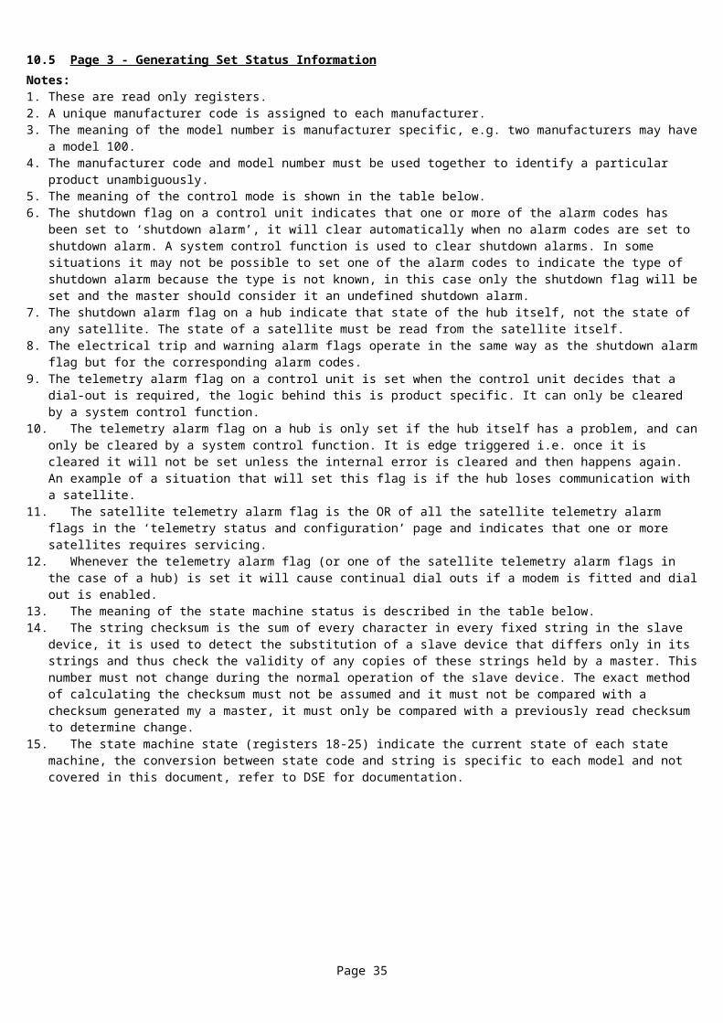
Type code
Type
0 Engine stopped1 Pre-Start2-6 Available for SAE assignment7 Not available
DPTC Action regeneration forcedType code
Type
0 Not active1 Active forced by switch2 Active forced by service tool3-6 Not Available7 Not available
CAN link status codesType code
Type
0 Link OK1 Link Lost2 Link Unknown65535 Unimplemented3-65534 Reserved
Page 35
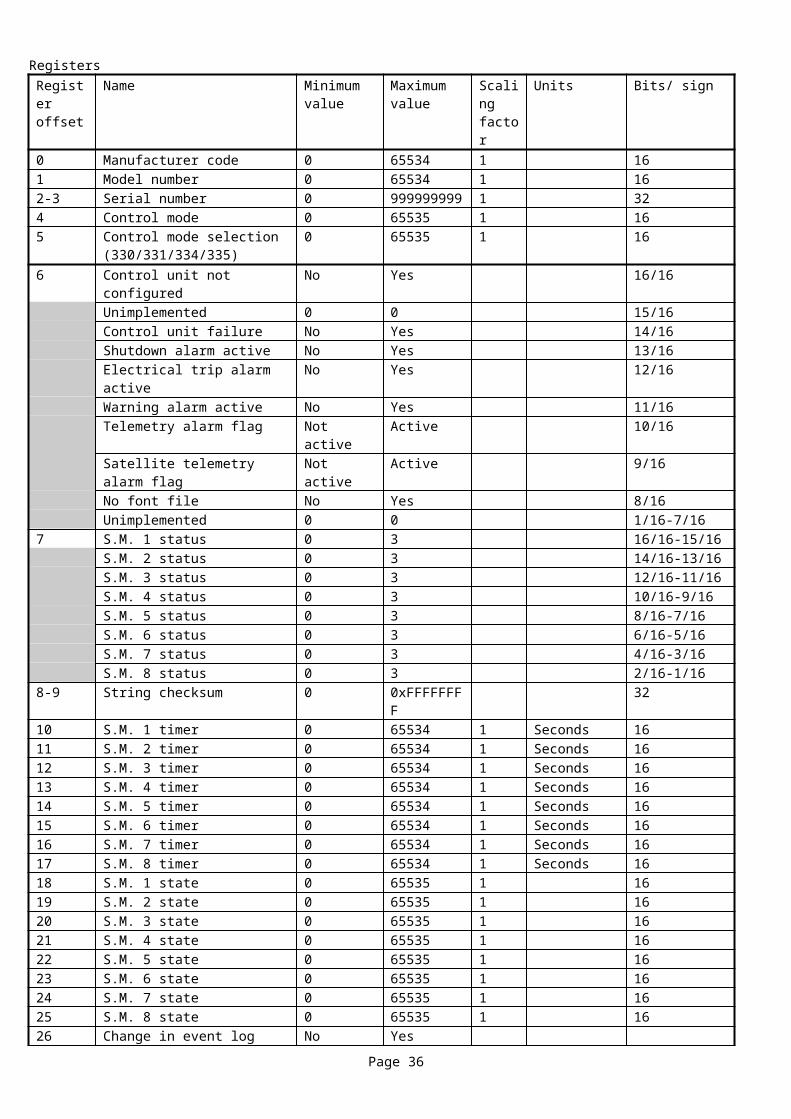
10.8 Page 6 - Derived Instrumentation Notes:1. These are read only registers.2. Registers 22, 23, 46, 47, 70 and 71 do indeed have limits of +/- 999.9%3. Registers 78-81 return 0 for leading, 1 for indeterminate, 2 for lagging (72xx/73xx only)4. Registers 85-108 have been added to support the 8680 although not all will be implemented initially.8xxx/74xx register allocation
Register offset
Name Minimum value
Maximum value
Scaling factor
Units Bits/ Sign
0-1 Generator total watts -99,999,999 99,999,999 1 W 32S2-3 Generator L1 VA 0 99,999,999 1 VA 324-5 Generator L2 VA 0 99,999,999 1 VA 32 6-7 Generator L3 VA 0 99,999,999 1 VA 328-9 Generator total VA 0 99,999,999 1 VA 32 10-11 Generator L1 VAr 0 99,999,999 1 VAr 3212-13 Generator L2 VAr 0 99,999,999 1 VAr 32 14-15 Generator L3 VAr 0 99,999,999 1 VAr 3216-17 Generator total VAr 0 99,999,999 1 VAr 32 18 Generator power factor L1 -1 1 0.01 16S19 Generator power factor L2 -1 1 0.01 16S20 Generator power factor L3 -1 1 0.01 16S21 Generator average power factor -1 1 0.01 16S22 Generator percentage of full
power-999.9 +999.9 0.1 % 16S
23 Generator percentage of full VAr -999.9 +999.9 0.1 % 16S24-25 Mains total watts -99,999,999 999,999,999 1 W 32S26-27 Mains L1 VA 0 99,999,999 1 VA 3228-29 Mains L2 VA 0 99,999,999 1 VA 32 30-31 Mains L3 VA 0 99,999,999 1 VA 3232-33 Mains total VA 0 999,999,999 1 VA 32 34-35 Mains L1 VAr 0 99,999,999 1 VAr 3236-37 Mains L2 VAr 0 99,999,999 1 VAr 32 38-39 Mains L3 VAr 0 99,999,999 1 VAr 3240-41 Mains total VAr 0 999,999,999 1 VAr 32 42 Mains power factor L1 -1 1 0.01 16S43 Mains power factor L2 -1 1 0.01 16S44 Mains power factor L3 -1 1 0.01 16S45 Mains average power factor -1 1 0.01 16S46 Mains percentage of full power -999.9 +999.9 0.1 % 16S47 Mains percentage of full VAr -999.9 +999.9 0.1 % 16S48-49 Bus total watts -999,999,999 999,999,999 1 W 32S50-51 Bus L1 VA 0 99,999,999 1 VA 3252-53 Bus L2 VA 0 99,999,999 1 VA 32 54-55 Bus L3 VA 0 99,999,999 1 VA 3256-57 Bus total VA 0 999,999,999 1 VA 32 58-59 Bus L1 VAr 0 99,999,999 1 VAr 3260-61 Bus L2 VAr 0 99,999,999 1 VAr 32 62-63 Bus L3 VAr 0 99,999,999 1 VAr 3264-65 Bus total VAr 0 999,999,999 1 VAr 32 66 Bus power factor L1 -1 1 0.01 16S67 Bus power factor L2 -1 1 0.01 16S68 Bus power factor L3 -1 1 0.01 16S69 Bus average power factor -1 1 0.01 16S70 Bus percentage of full power -999.9 +999.9 0.1 % 16S71 Bus percentage of full VAr -999.9 +999.9 0.1 % 16S72-73 Load total watts -999,999,999 999,999,999 1 W 32S74-75 Load total VAr 0 999,999,999 1 VAr 32
Page 36
Derived Instrumentation Continued76 Mains R.O.C.O.F. 0 10.00 0.01 Hz/s 1677 Mains vector shift 0 360.0 0.1 Degrees 1678 Gen L1 lead /lag 0 2 1679 Gen L2 lead /lag 0 2 1680 Gen L3 lead /lag 0 2 1681 Gen total lead /lag 0 2 1682 Gen L1 percentage of full power -999.9 +999.9 0.1 % 16S83 Gen L2 percentage of full power -999.9 +999.9 0.1 % 16S84 Gen L3 percentage of full power -999.9 +999.9 0.1 % 16S85 Bus 2 average power factor -1 1 0.01 16S86-87 Bus 2 total watts -999,999,999 999,999,999 1 W 32S88-89 Bus 2 L1 VA 0 99,999,999 1 VA 3290-91 Bus 2 L2 VA 0 99,999,999 1 VA 32 92-93 Bus 2 L3 VA 0 99,999,999 1 VA 3294-95 Bus 2 total VA 0 999,999,999 1 VA 32 96-97 Bus 2 L1 VAr 0 99,999,999 1 VAr 3298-99 Bus 2 L2 VAr 0 99,999,999 1 VAr 32 100-101 Bus 2 L3 VAr 0 99,999,999 1 VAr 32102-103 Bus 2 total VAr 0 999,999,999 1 VAr 32 104 Bus 2 power factor L1 -1 1 0.01 16S105 Bus 2 power factor L2 -1 1 0.01 16S106 Bus 2 power factor L3 -1 1 0.01 16S107 Bus 2 percentage of full power -999.9 +999.9 0.1 % 16S108 Bus 2 percentage of full VAr -999.9 +999.9 0.1 % 16S109 Mains L1 lead/lag 0 2 16110 Mains L2 lead/lag 0 2 16111 Mains L3 lead/lag 0 2 16112 Mains total lead/lag 0 2 16113-255 Reserved
Page 37
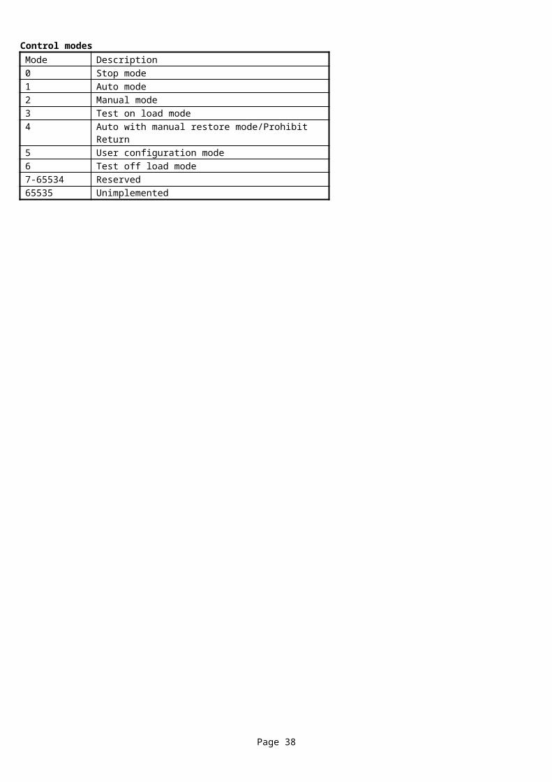
3xx register allocationRegister offset
Name Minimum value
Maximum value
Scaling factor
Units Bits/ Sign
0-1 S2 total watts -99,999,999 99,999,999 1 W 32S2-3 S2 L1 VA 0 99,999,999 1 VA 324-5 S2 L2 VA 0 99,999,999 1 VA 32 6-7 S2 L3 VA 0 99,999,999 1 VA 328-9 S2 total VA 0 99,999,999 1 VA 32 10-11 S2 L1 VAr 0 99,999,999 1 VAr 3212-13 S2 L2 VAr 0 99,999,999 1 VAr 32 14-15 S2 L3 VAr 0 99,999,999 1 VAr 3216-17 S2 total VAr 0 99,999,999 1 VAr 32 18 S2 power factor L1 -1 1 0.01 16S19 S2 power factor L2 -1 1 0.01 16S20 S2 power factor L3 -1 1 0.01 16S21 S2 average power factor -1 1 0.01 16S22 S2 percentage of full power -999.9 +999.9 0.1 % 16S23 S2 percentage of full VAr -999.9 +999.9 0.1 % 16S24-25 S1 total watts -99,999,999 999,999,999 1 W 32S26-27 S1 L1 VA 0 99,999,999 1 VA 3228-29 S1 L2 VA 0 99,999,999 1 VA 32 30-31 S1 L3 VA 0 99,999,999 1 VA 3232-33 S1 total VA 0 999,999,999 1 VA 32 34-35 S1 L1 VAr 0 99,999,999 1 VAr 3236-37 S1 L2 VAr 0 99,999,999 1 VAr 32 38-39 S1 L3 VAr 0 99,999,999 1 VAr 3240-41 S1 total VAr 0 999,999,999 1 VAr 32 42 S1 power factor L1 -1 1 0.01 16S43 S1 power factor L2 -1 1 0.01 16S44 S1 power factor L3 -1 1 0.01 16S45 S1 average power factor -1 1 0.01 16S46 S1 percentage of full power -999.9 +999.9 0.1 % 16S47 S1 percentage of full VAr -999.9 +999.9 0.1 % 16S48-49 Unimplemented (signed 32) 32S50-65 Unimplemented (unsigned 32) 3266-71 Unimplemented (signed 16) 16S72-73 Unimplemented (signed 32) 32S74-75 Unimplemented (unsigned 32) 3276-77 Unimplemented (unsigned 16) 1678 S2 L1 lead /lag 0 2 1679 S2 L2 lead /lag 0 2 1680 S2 L3 lead /lag 0 2 1681 S2 total lead /lag 0 2 1682 S2 L1 percentage of full power -999.9 +999.9 0.1 % 16S83 S2 L2 percentage of full power -999.9 +999.9 0.1 % 16S84 S2 L3 percentage of full power -999.9 +999.9 0.1 % 16S85 Unimplemented (signed 16) 16S86-87 Unimplemented (signed 32) 32S88-103 Unimplemented (unsigned 32) 32104-108 Unimplemented (signed 16) 16S109 S1L1 lead/lag 0 2 16110 S1L2 lead/lag 0 2 16111 S1L3 lead/lag 0 2 16112 S1total lead/lag 0 2 16113-255 Reserved
Page 38
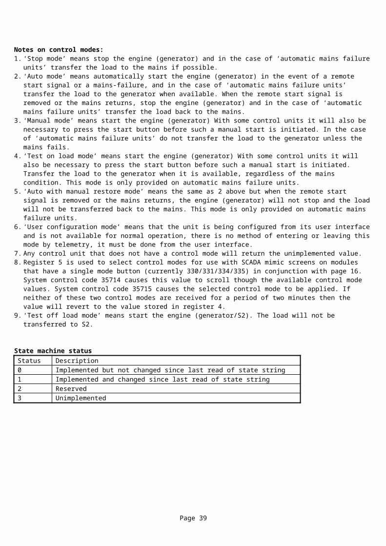
10.9 Page 7 - Accumulated Instrumentation Notes:1. These are read/write registers though some systems may not support writing to some registers.
8xxx/74xx register allocationRegister offset
Name Minimum value
Maximum value
Scaling factor
Units Bits/ Sign
0-1 Current time since 1/1/70 0 4.29 x10⁹ 1 Seconds 322-3 Time to next maintenance -2.14 x10⁹ 2.14 x10⁹ 1 Seconds 32S4-5 Time of next maintenance since 1/1/70 0 4.29 x10⁹ 1 Seconds 326-7 Engine run time 0 4.29 x10⁹ 1 Seconds 328-9 Generator positive KW hours 0 4.29 x10⁹ 0.1 KW hour 3210-11 Generator negative KW hours 0 4.29 x10⁹ 0.1 KW hour 3212-13 Generator KVA hours 0 4.29 x10⁹ 0.1 KVA hour 3214-15 Generator KVAr hours 0 4.29 x10⁹ 0.1 KVAr hour 3216-17 Number of starts 0 99999 3218-19 Mains positive KW hours 0 4.29 x10⁹ 0.1 KW hour 3220-21 Mains negative KW hours 0 4.29 x10⁹ 0.1 KW hour 3222-23 Mains KVA hours 0 4.29 x10⁹ 0.1 KVA hour 3224-25 Mains KVAr hours 0 4.29 x10⁹ 0.1 KVAr hour 3226-27 Bus positive KW hours 0 4.29 x10⁹ 0.1 KW hour 3228-29 Bus negative KW hours 0 4.29 x10⁹ 0.1 KW hour 3230-31 Bus KVA hours 0 4.29 x10⁹ 0.1 KVA hour 3232-33 Bus KVAr hours 0 4.29 x10⁹ 0.1 KVAr hour 3234-35 Fuel used 0 4.29 x10⁹ 1 Litre 3236-37 Maximum positive mains R.O.C.O.F. 0 10.00 0.01 Hz/s 3238-39 Maximum negative mains R.O.C.O.F. 0 10.00 0.01 Hz/s 3240-41 Maximum positive mains vector shift 0 360.0 0.1 Degrees 3242-43 Maximum negative mains vector shift 0 360.0 0.1 Degrees 3244-45 Time to next maintenance alarm 1 -2.14 x10⁹ 2.14 x10⁹ 1 Seconds 32S46-47 Time of next maintenance alarm 1 since
1/1/700 4.29 x10⁹ 1 Seconds 32
48-49 Time to next maintenance alarm 2 -2.14 x10⁹ 2.14 x10⁹ 1 Seconds 32S50-51 Time of next maintenance alarm 2 since
1/1/700 4.29 x10⁹ 1 Seconds 32
52-53 Time to next maintenance alarm 3 -2.14 x10⁹ 2.14 x10⁹ 1 Seconds 32S54-55 Time of next maintenance alarm 3 since
1/1/700 4.29 x10⁹ 1 Seconds 32
56-255 Reserved
Page 39
3xx register allocationRegister offset
Name Minimum value
Maximum value
Scaling factor
Units Bits/ Sign
0-1 Current time since 1/1/70 0 4.29 x10⁹ 1 Seconds 322-7 Unimplemented (Reserved for future use) 328-9 S2 positive KW hours 0 4.29 x10⁹ 0.1 KW hour 3210-11 Unimplemented (Reserved for future use) 3212-13 S2 KVA hours 0 4.29 x10⁹ 0.1 KVA hour 3214-15 S2 KVAr hours 0 4.29 x10⁹ 0.1 KVAr hour 3216-17 Unimplemented (Reserved for future use) 2318-19 S1 positive KW hours 0 4.29 x10⁹ 0.1 KW hour 3220-21 Unimplemented (Reserved for future use) 2322-23 S1 KVA hours 0 4.29 x10⁹ 0.1 KVA hour 3224-25 S1 KVAr hours 0 4.29 x10⁹ 0.1 KVAr hour 3226-55 Unimplemented (Reserved for future use) 3256-255 Reserved
Page 40
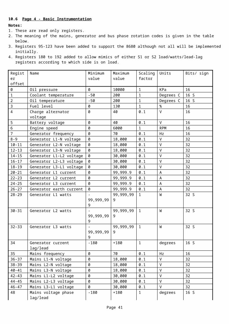
10.10 Page 8 - Alarm Conditions Notes:1. These are read only registers.2. This is the old alarm system, for 72x/73xx and 8xxx/74xx families page 154 should be used instead.3. Each alarm can be in one of 15 conditions as shown in the table below.4. Registers 1-32 contain the status of named, internally generated, alarms and indications. These may be extended by future versions
of GenComm and any software that reads them must be able to cope with such extensions. This is possible because register 0 specifies the number of pre-defined internal alarm conditions that are implemented on a slave device, the software should read and process the specified number. The software does not need to know the definitions of any new alarms since it can read the alarms strings and display them as specified by the alarm condition. All unimplemented pre-defined alarms return the unimplemented value 15, not an exception.
5. Registers 129-160 contain the status of unnamed digital inputs. Register 128 specifies the number of unnamed digital inputs and any software that reads them must be able to cope with all 128 in the same way as for the pre-defined alarms. All unimplemented digital inputs up to 128 will return the unimplemented value 15, not an exception.
6. Each alarm has 2 strings in pages 32-95 which can be displayed on a PC for example, the alarm code specifies which string it is appropriate to display.
7. The contents of alarm strings will never change while the slave device is operating so a copy can be held by the master to minimise traffic.
RegistersRegister offset
Name Minimum value Maximum value Bits/ Sign
0 Number of named alarms 97 128 161 Emergency stop 0 15 13/16-16/16
Low oil pressure 0 15 9/16-12/16High coolant temperature 0 15 5/16-8/16High oil temperature 0 15 1/16-4/16
2 Under speed 0 15 13/16-16/16Over speed 0 15 9/16-12/16Fail to start 0 15 5/16-8/16Fail to come to rest 0 15 1/16-4/16
3 Loss of speed sensing 0 15 13/16-16/16Generator low voltage 0 15 9/16-12/16Generator high voltage 0 15 5/16-8/16Generator low frequency 0 15 1/16-4/16
4 Generator high frequency 0 15 13/16-16/16Generator high current 0 15 9/16-12/16Generator earth fault 0 15 5/16-8/16Generator reverse power 0 15 1/16-4/16
5 Air flap 0 15 13/16-16/16Oil pressure sender fault 0 15 9/16-12/16Coolant temperature sender fault 0 15 5/16-8/16Oil temperature sender fault 0 15 1/16-4/16
6 Fuel level sender fault 0 15 13/16-16/16Magnetic pickup fault 0 15 9/16-12/16Loss of AC speed signal 0 15 5/16-8/16Charge alternator failure 0 15 1/16-4/16
7 Low battery voltage 0 15 13/16-16/16High battery voltage 0 15 9/16-12/16Low fuel level 0 15 5/16-8/16High fuel level 0 15 1/16-4/16
Page 41
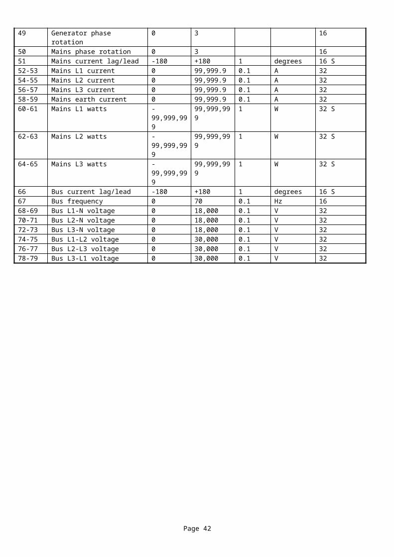
Page 8 registers continued8 Generator failed to close 0 15 13/16-16/16
Mains failed to close 0 15 9/16-12/16Generator failed to open 0 15 5/16-8/16Mains failed to open 0 15 1/16-4/16
9 Mains low voltage 0 15 13/16-16/16Mains high voltage 0 15 9/16-12/16Bus failed to close 0 15 5/16-8/16Bus failed to open 0 15 1/16-4/16
10 Mains low frequency 0 15 13/16-16/16Mains high frequency 0 15 9/16-12/16Mains failed 0 15 5/16-8/16Mains phase rotation wrong 0 15 1/16-4/16
11 Generator phase rotation wrong 0 15 13/16-16/16Maintenance due 0 15 9/16-12/16Clock not set 0 15 5/16-8/16Local LCD configuration lost 0 15 1/16-4/16
12 Local telemetry configuration lost 0 15 13/16-16/16Control unit not calibrated 0 15 9/16-12/16Modem power fault 0 15 5/16-8/16Generator short circuit 0 15 1/16-4/16
13 Failure to synchronise 0 15 13/16-16/16Bus live 0 15 9/16-12/16Scheduled run 0 15 5/16-8/16Bus phase rotation wrong 0 15 1/16-4/16
14 Priority selection error 0 15 13/16-16/16Multiset communications (MSC) data error 0 15 9/16-12/16Multiset communications (MSC) ID error 0 15 5/16-8/16Multiset communications (MSC) failure 0 15 1/16-4/16
15 Multiset communications (MSC) too few sets 0 15 13/16-16/16Multiset communications (MSC) alarms inhibited 0 15 9/16-12/16Multiset communications (MSC) old version units 0 15 5/16-8/16Mains reverse power 0 15 1/16-4/16
16 Minimum sets not reached 0 15 13/16-16/16Insufficient capacity available 0 15 9/16-12/16Expansion input unit not calibrated 0 15 5/16-8/16Expansion input unit failure 0 15 1/16-4/16
17 Auxiliary sender 1 low 0 15 13/16-16/16Auxiliary sender 1 high 0 15 9/16-12/16Auxiliary sender 1 fault 0 15 5/16-8/16Auxiliary sender 2 low 0 15 1/16-4/16
18 Auxiliary sender 2 high 0 15 13/16-16/16Auxiliary sender 2 fault 0 15 9/16-12/16Auxiliary sender 3 low 0 15 5/16-8/16Auxiliary sender 3 high 0 15 1/16-4/16
19 Auxiliary sender 3 fault 0 15 13/16-16/16Auxiliary sender 4 low 0 15 9/16-12/16Auxiliary sender 4 high 0 15 5/16-8/16Auxiliary sender 4 fault 0 15 1/16-4/16
20 Engine control unit (ECU) link lost 0 15 13/16-16/16Engine control unit (ECU) failure 0 15 9/16-12/16Engine control unit (ECU) error 0 15 5/16-8/16Low coolant temperature 0 15 1/16-4/16
21 Out of sync 0 15 13/16-16/16Low Oil Pressure Switch 0 15 9/16-12/16Alternative Auxiliary Mains Fail 0 15 5/16-8/16Loss of excitation 0 15 1/16-4/16
Page 42

Page 8 registers continued22 Mains kW Limit 0 15 13/16-16/16
Negative phase sequence 0 15 9/16-12/16Mains ROCOF 0 15 5/16-8/16Mains vector shift 0 15 1/16-4/16
23 Mains G59 low frequency 0 15 13/16-16/16Mains G59 high frequency 0 15 9/16-12/16Mains G59 low voltage 0 15 5/16-8/16Mains G59 high voltage 0 15 1/16-4/16
24 Mains G59 trip 0 15 13/16-16/16Generator kW Overload 0 15 9/16-12/16Engine Inlet Temperature high 0 15 5/16-8/16Bus 1 live 0 15 1/16-4/16
25 Bus 1 phase rotation wrong 0 15 13/16-16/16Bus 2 live 0 15 9/16-12/16Bus 2 phase rotation wrong 0 15 5/16-8/16Reserved 0 15 1/16-4/16
26-32 Unimplemented33-127 Reserved
Page 43
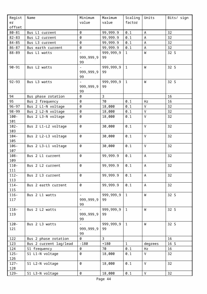
Page 8 registers continued128 Number of unnamed digital inputs 0 128 16129 Unnamed digital input 1 0 15 13/16-16/16
Unnamed digital input 2 0 15 9/16-12/16Unnamed digital input 3 0 15 5/16-8/16Unnamed digital input 4 0 15 1/16-4/16
130 Unnamed digital input 5 0 15 13/16-16/16Unnamed digital input 6 0 15 9/16-12/16Unnamed digital input 7 0 15 5/16-8/16Unnamed digital input 8 0 15 1/16-4/16
131 Unnamed digital input 9 0 15 13/16-16/16Unnamed digital input 10 0 15 9/16-12/16Unnamed digital input 11 0 15 5/16-8/16Unnamed digital input 12 0 15 1/16-4/16
132 Unnamed digital input 13 0 15 13/16-16/16Unnamed digital input 14 0 15 9/16-12/16Unnamed digital input 15 0 15 5/16-8/16Unnamed digital input 16 0 15 1/16-4/16
133 Unnamed digital inputs 17-20 0 15 16134 Unnamed digital inputs 21-24 0 15 16135 Unnamed digital inputs 25-28 0 15 16136 Unnamed digital inputs 29-32 0 15 16137 Unnamed digital inputs 33-36 0 15 16138 Unnamed digital inputs 37-40 0 15 16139 Unnamed digital inputs 41-44 0 15 16140 Unnamed digital inputs 45-48 0 15 16141 Unnamed digital inputs 49-52 0 15 16142 Unnamed digital inputs 53-56 0 15 16143 Unnamed digital inputs 57-60 0 15 16144 Unnamed digital inputs 61-64 0 15 16145 Unnamed digital inputs 65-68 0 15 16146 Unnamed digital inputs 69-72 0 15 16147 Unnamed digital inputs 73-76 0 15 16148 Unnamed digital inputs 77-80 0 15 16149 Unnamed digital inputs 81-84 0 15 16150 Unnamed digital inputs 85-88 0 15 16151 Unnamed digital inputs 89-92 0 15 16152 Unnamed digital inputs 93-96 0 15 16153 Unnamed digital inputs 97-100 0 15 16154 Unnamed digital inputs 101-104 0 15 16155 Unnamed digital inputs 105-108 0 15 16156 Unnamed digital inputs 109-112 0 15 16157 Unnamed digital inputs 113-116 0 15 16158 Unnamed digital inputs 117-120 0 15 16159 Unnamed digital inputs 121-124 0 15 16160 Unnamed digital inputs 125-128 0 15 16161-255 Reserved
Page 44
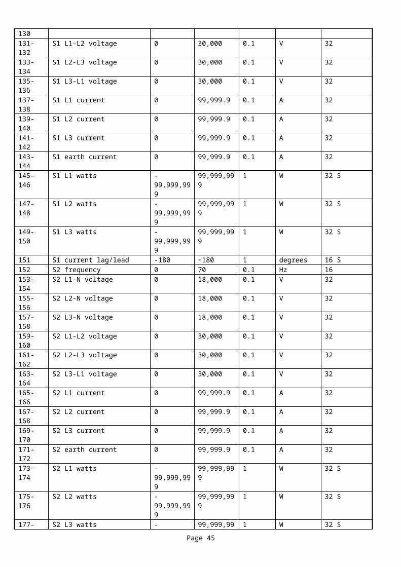
Alarm condition codesCondition Meaning Displayed string0 Disabled digital input None1 Not active alarm None2 Warning alarm Active string3 Shutdown alarm Active string4 Electrical trip alarm Active string5-7 Reserved8 Inactive indication (no string) None9 Inactive indication (displayed string) Inactive string10 Active indication Active string11-14 Reserved15 Unimplemented alarm None
Notes on alarm codes1. An alarm that is fitted but disabled by the configuration of the slave device returns code 0.2. An alarm that is not implemented on a particular control unit returns code 15.3. An indication that does not require a message to be displayed when inactive returns either code 8 or 10.4. An indication that does require a message to be displayed when inactive returns either code 9 or 10. 5. The inactive strings are only required for indications, in all other cases they will contain 32 spaces.
10.11 Page 9 – Total Harmonic Distortion Notes:1. These are read only registers.2. Only supported on 88xx/84xx modules at present (introduced at version 1.0 of these modules)3. 8810/8410 don’t support registers 120-131 – they will return Unimplemented (sentinel value)
RegistersRegister offset
Name Minimum value
Maximum value
Scaling factor
Units Bits/ Sign
0 V1 Voltage L1 THD 0 10000 0.01 % 161 V1 Voltage L1 Fundamental level 0 100 1 162 V1 Voltage L1 3rd harmonic level 0 100 1 163 V1 Voltage L1 5th harmonic level 0 100 1 164 V1 Voltage L1 7th harmonic level 0 100 1 165 V1 Voltage L1 9th harmonic level 0 100 1 166 V1 Voltage L1 11th harmonic level 0 100 1 167 V1 Voltage L1 13th harmonic level 0 100 1 168 V1 Voltage L1 15th harmonic level 0 100 1 169 V1 Voltage L1 17th harmonic level 0 100 1 1610 V1 Voltage L1 19th harmonic level 0 100 1 1611 V1 Voltage L1 21st harmonic level 0 100 1 1612-23 V1 Voltage L2 THD etc24-35 V1 Voltage L3 THD etc36-47 V2 Voltage L1 THD etc48-59 V2 Voltage L2 THD etc60-71 V2 Voltage L3 THD etc72-83 Current L1 THD etc84-95 Current L2 THD etc96-107 Current L3 THD etc108-119 Current Neutral/Earth THD etc120-131 Current 5th CT THD etc132-255 Reserved
Page 45
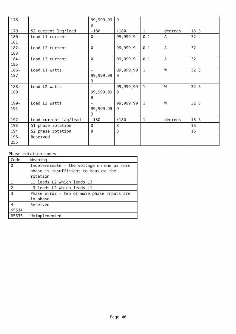
10.12 Page 11 - Diagnostic - General Notes:4. These are read only registers.5. Register 0 gives the version as major/minor, with the major version in the upper 8 bits, the minor version in the lower 8 bits.
RegistersRegister offset
Name Minimum value
Maximum value
Scaling factor
Units Bits/ Sign
0 Software version 0 9999 0.01 161 CPU power usage 0 200 1 % 162 Button number pressed, 0=none 0 255 1 163 Backup supply voltage 0 40 0.1 V 164-255 Reserved
10.13 Page 12 - Diagnostic - Digital Inputs Notes1. These are read only registers.2. These registers represent the state of the actual inputs to the control unit before the application of any time delays or other processing
and are intended for diagnostic purposes only.3. The number of named digital inputs may be increased in future versions of GenComm. Manufacturers may not add their own to the
list of named inputs as there are no corresponding strings to identify them. Any inputs that are required but not named must be included in the list of unnamed digital inputs.
4. The meaning of the named digital input codes is shown in the table below.5. Register 16 indicates the number of unnamed digital inputs that are supported, any software that displays these must cope with any
number up to 128. Each is represented by only one bit as there is no need to indicate that it is unimplemented.6. Unimplemented inputs (including totally unimplemented registers) return 3, not an exception.
Page 46

RegistersRegister offset
Name Minimum value
Maximum value
Scaling factor
Units Bits/ Sign
0 Emergency stop input 0 3 15/16-16/16Low oil pressure switch input 0 3 13/16-14/16High engine temp. switch input 0 3 11/16-12/16Remote start input 0 3 9/16-10/16Remote fuel on input 0 3 7/16-8/16Lamp test input 0 3 5/16-6/16Reset input 0 3 3/16-4/16Panel lock input 0 3 1/16-2/16
1 Start button input 0 3 15/16-16/16Stop button input 0 3 13/16-14/16Transfer to generator button input 0 3 11/16-12/16Transfer to mains button input 0 3 9/16-10/16Unimplemented 3 3 7/16-8/16Unimplemented 3 3 5/16-6/16Unimplemented 3 3 3/16-4/16Unimplemented 3 3 1/16-2/16
2-15 Reserved 1616 Number of unnamed digital inputs 0 128 1617 Unnamed digital input 1 Open Closed 16/16
Unnamed digital input 2 Open Closed 15/16Unnamed digital input 3 Open Closed 14/16Unnamed digital input 4 Open Closed 13/16Unnamed digital input 5 Open Closed 12/16Unnamed digital input 6 Open Closed 11/16Unnamed digital input 7 Open Closed 10/16Unnamed digital input 8 Open Closed 9/16Unnamed digital input 9 Open Closed 8/16Unnamed digital input 10 Open Closed 7/16Unnamed digital input 11 Open Closed 6/16Unnamed digital input 12 Open Closed 5/16Unnamed digital input 13 Open Closed 4/16Unnamed digital input 14 Open Closed 3/16Unnamed digital input 15 Open Closed 2/16Unnamed digital input 16 Open Closed 1/16
18 Unnamed digital input 17-32 Open Closed 1619 Unnamed digital input 33-48 Open Closed 1620 Unnamed digital input 49-64 Open Closed 1621 Unnamed digital input 65-80 Open Closed 1622 Unnamed digital input 81-96 Open Closed 1623 Unnamed digital input 97-112 Open Closed 1624 Unnamed digital input 113-128 Open Closed 1625-255 Reserved
Named digital input codesCode Meaning0 Open1 Closed2 Reserved3 Unimplemented
Page 47
10.14 Page 13 - Diagnostic - Digital Outputs Notes:1. Generally these are read only registers to avoid conflict between the slave devices chosen output state and commands from a master.
However, in some cases a slave device may accept write commands to these registers, e.g. a hub may have digital outputs which are not controlled by the hub itself but from a master device. A slave device may only accept write commands to these registers if this does not cause a conflict with internally generated controls of the outputs.
2. These registers represent the state of the actual digital outputs of the control unit after any internal processing and are primarily intended for diagnostic purposes only (but see note 1).
3. The number of named outputs may be increased in future versions of GenComm. Manufacturers may not add their own to the list of named outputs as there are no corresponding strings to identify them. Any outputs that are required but not named must be included in the list of unnamed digital outputs.
4. The meaning of the named digital output codes is shown in the table below.5. Register 16 indicates the number of unnamed digital outputs that are supported, any software that displays these must cope with any
number up to 128. Each is represented by only one bit as there is no need to indicate that it is unimplemented.6. Unimplemented outputs (including totally unimplemented registers) return 3, not an exception.
RegistersRegister offset
Name Minimum value
Maximum value
Scaling factor
Units Bits/ Sign
0 Fuel relay 0 3 15/16-16/16Start relay 0 3 13/16-14/16Mains loading relay 0 3 11/16-12/16Generator loading relay 0 3 9/16-10/16Modem power relay 0 3 7/16-8/16Unimplemented 3 3 5/16-6/16Unimplemented 3 3 3/16-4/16Unimplemented 3 3 1/16-2/16
1-15 Reserved 3 3 1616 Number of unnamed digital outputs 0 128 1617 Unnamed digital output 1 De-energised Energised 16/16
Unnamed digital output 2 De-energised Energised 15/16Unnamed digital output 3 De-energised Energised 14/16Unnamed digital output 4 De-energised Energised 13/16Unnamed digital output 5 De-energised Energised 12/16Unnamed digital output 6 De-energised Energised 11/16Unnamed digital output 7 De-energised Energised 10/16Unnamed digital output 8 De-energised Energised 9/16Unnamed digital output 9 De-energised Energised 8/16Unnamed digital output 10 De-energised Energised 7/16Unnamed digital output 11 De-energised Energised 6/16Unnamed digital output 12 De-energised Energised 5/16Unnamed digital output 13 De-energised Energised 4/16Unnamed digital output 14 De-energised Energised 3/16Unnamed digital output 15 De-energised Energised 2/16Unnamed digital output 16 De-energised Energised 1/16
18 Unnamed digital output 17-32 De-energised Energised 1619 Unnamed digital output 33-48 De-energised Energised 1620 Unnamed digital output 49-64 De-energised Energised 1621 Unnamed digital output 65-80 De-energised Energised 1622 Unnamed digital output 81-96 De-energised Energised 1623 Unnamed digital output 97-112 De-energised Energised 1624 Unnamed digital output 113-128 De-energised Energised 1625-255 Reserved
Named digital output codesCode Meaning0 De-energised1 Energised2 Reserved3 Unimplemented
Page 48
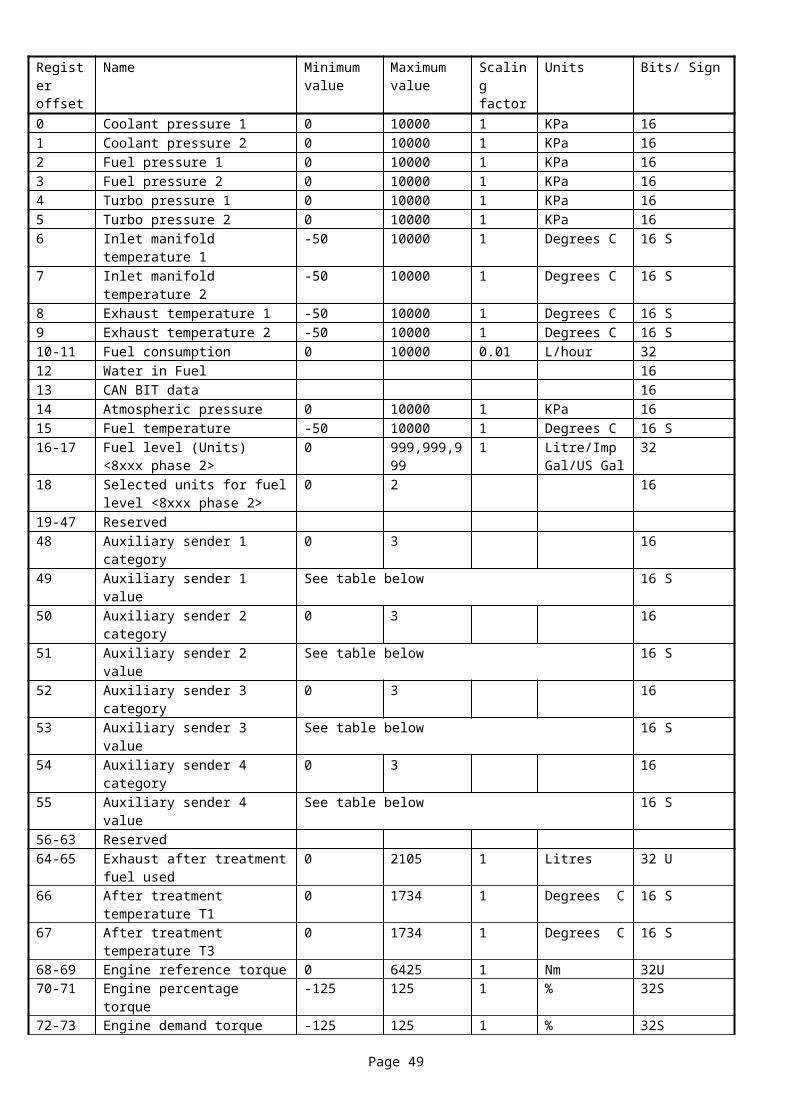
10.15 Page 14 - Diagnostic - LEDs Notes:1. Generally these are read only registers to avoid conflict between the slave devices chosen LED state and commands from a master.
However, in some cases a slave device may accept write commands to these registers, e.g. a hub may have LEDs which are not controlled by the hub itself but from a master device. A slave device may only accept write commands to these registers if this does not cause a conflict with internally generated controls of the outputs.
2. These registers represent the state of the actual LEDs on the control unit after any internal processing and are primarily intended for diagnostic purposes only (but see note 1).
3. Register 0 indicates the number of LEDs that are supported, any software that displays these must cope with any number up to 128.4. Unimplemented LEDs (including totally unimplemented registers) return 15, not an exception.
RegistersRegister offset
Name Minimum value
Maximum value
Scaling factor
Units Bits/ Sign
0 Number of LEDs 0 128 161 LED 1 colour (see table below) 0 15 13/16-16/16
LED 2 colour 0 15 9/16-12/16LED 3 colour 0 15 5/16-8/16LED 4 colour 0 15 1/16-4/16
2 LEDs 5-8 colour 0 15 163 LEDs 9-12 colour 0 15 164 LEDs 13-16 colour 0 15 165 LEDs 17-20 colour 0 15 166 LEDs 21-24 colour 0 15 167 LEDs 25-28 colour 0 15 168 LEDs 29-32 colour 0 15 169 LEDs 33-36 colour 0 15 1610 LEDs 37-40 colour 0 15 1611 LEDs 41-44 colour 0 15 1612 LEDs 45-48 colour 0 15 1613 LEDs 49-52 colour 0 15 1614 LEDs 53-56 colour 0 15 1615 LEDs 57-60 colour 0 15 1616 LEDs 61-64 colour 0 15 1617 LEDs 65-68 colour 0 15 1618 LEDs 69-72 colour 0 15 1619 LEDs 73-76 colour 0 15 1620 LEDs 77-80 colour 0 15 1621 LEDs 81-84 colour 0 15 1622 LEDs 85-88 colour 0 15 1623 LEDs 89-92 colour 0 15 1624 LEDs 93-96 colour 0 15 1625 LEDs 97-100 colour 0 15 1626 LEDs 101-104 colour 0 15 1627 LEDs 105-108 colour 0 15 1628 LEDs 109-112 colour 0 15 1629 LEDs 113-116 colour 0 15 1630 LEDs 117-120 colour 0 15 1631 LEDs 121-124 colour 0 15 1632 LEDs 125-128 colour 0 15 1633-255 Reserved
Page 49
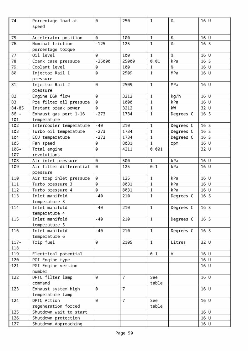
LED coloursCode Colour 0 Not lit1 Reserved2 Red3 Orange4 Yellow5 Green6 Blue7 Purple8 Reserved9 White10 Reserved11 Reserved12 Reserved13 Reserved14 Reserved15 Unimplemented LED
Page 50
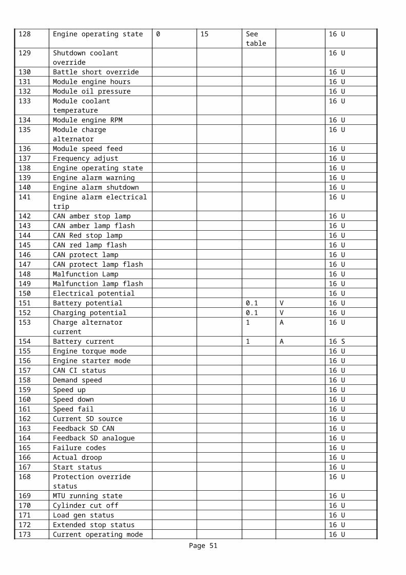
10.16 Page 16 - Control Registers Notes:1. These are a mixture of read only and write only registers.2. Registers 0 to 7 contain flags that indicate the available system control functions. If a bit is set the corresponding function code is
available.3. One of the system control keys from the table below must be written into register 8 and its ones-compliment written into register 9
with a single function 16 (write multiple registers) to perform the specified system control function.4. Writing any other value or using a function that is not available will return extended exception code 7 (Illegal value written to
register) and have no affect.5. Function codes 0 to 31 perform exactly the same function as pressing the equivalent button on the control unit.6. Function 34 ‘reset alarms’ is not the same as function 7. The former resets any alarm condition codes that can be reset. The latter
simulates a button which may or may not exist on the control unit, if it does not exist it will have no affect. If all alarm condition codes are able to be reset the shutdown, electrical trip and warning alarm active flags (as appropriate) in page 3 will consequently reset.
7. Function 34 does not under any circumstances reset the telemetry alarm flag in page 3, function 35 must be used for this.8. Locking the user controls stops the buttons corresponding to function codes 0-31 from operating and stops any attempt to configure
the unit from the user controls. It does not stop the user from viewing status information and instrumentation values.9. Function 38 resets the Page 7 values ‘Time to next maintenance’ and ‘Time of next maintenance since 1/1/70’. The reset values are
manufacturer specific, if it is desired to set one of these two items to a specific value then they can be directly written to in Page 7.10. Function 10 resets only those alarms associated with the detection of mains failure while running in parallel with the mains, i.e. G59
alarms and ROCOF and vector shift.11. Function 43 is used to register an 8721 display unit with an 8700 module.12. Function 44 is used to register an 8711 display unit with an 8700 module.13. Function 45 is used to register an 8716 display unit with an 8700 module.14. Functions 46,47 & 48 are used as part of the data logging functionality (of the 8xxx/74xx family)
RegistersRegister offset
Name Minimum value
Maximum value
Scaling factor
Units Bits/ Sign Read/write
0 System control function 0 supported 0 1 16/16 Read onlySystem control function 1 supported 0 1 15/16 Read onlySystem control function 2 supported 0 1 14/16 Read onlySystem control function 3 supported 0 1 13/16 Read onlySystem control function 4 supported 0 1 12/16 Read onlySystem control function 5 supported 0 1 11/16 Read onlySystem control function 6 supported 0 1 10/16 Read onlySystem control function 7 supported 0 1 9/16 Read onlySystem control function 8 supported 0 1 8/16 Read onlySystem control function 9 supported 0 1 7/16 Read onlySystem control function 10 supported 0 1 6/16 Read onlySystem control function 11 supported 0 1 5/16 Read onlySystem control function 12 supported 0 1 4/16 Read onlySystem control function 13 supported 0 1 3/16 Read onlySystem control function 14 supported 0 1 2/16 Read onlySystem control function 15 supported 0 1 1/16 Read only
1 System control function 16-31 supported 0 65535 16 Read only2 System control function 32-47 supported 0 65535 16 Read only3 System control function 48-63 supported 0 65535 16 Read only4 System control function 64-79 supported 0 65535 16 Read only5 System control function 80-95 supported 0 65535 16 Read only6 System control function 96-111supported 0 65535 16 Read only7 System control function 112-127
supported0 65535 16 Read only
8 System control key 0 65535 16 Write only9 Compliment of system control key 0 65535 16 Write only10-255 Reserved
Page 51
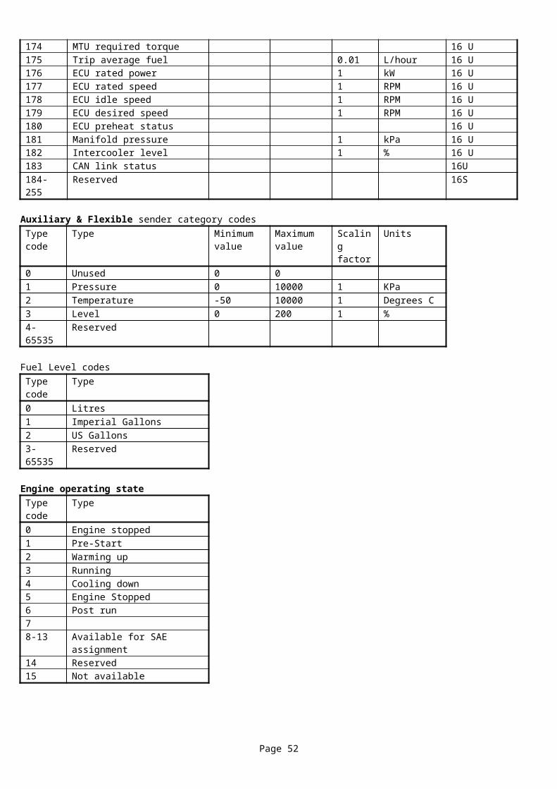
System control keysFunction code
System control function System control key
0 Select Stop mode 357001 Select Auto mode 357012 Select Manual mode 357023 Select Test on load mode 357034 Select Auto with manual restore mode 357045 Start engine if in manual or test modes 357056 Mute alarm 357067 Reset alarms 357078 Transfer to generator 357089 Transfer to mains 3570910 Reset mains failure 3571011 Close Bus (Bus Tie Controller) 3571112 Open Bus (Bus Tie Controller) 3571213 Toggle Bus Open/Closed (Bus Tie Controller) 3571314 Scroll through mode selections (mode button on 330/331/334/335) 3571415 Enable selected mode (scroll button on 330/331/334/335) 3571516-31 Reserved 35716-3573132 Telemetry start if in auto mode 3573233 Cancel telemetry start in auto mode 3573334 Reset alarms 3573435 Clear telemetry alarm flag 3573536 Lock the user controls 3573637 Unlock the user controls 3573738 Reset the maintenance alarm 1 due times 3573839 MSC alarm inhibit on 3573940 MSC alarm inhibit off 3574041 Reset the maintenance alarm 2 due times 3574142 Reset the maintenance alarm 3 due times 3574243 8721 Display unit registered/alive 3574344 8711 Display unit registered/alive 3574445 8716 Display unit registered/alive 3574546 Start data logging (temporarily overrides the module state) 3574647 Stop data logging (temporarily overrides the module state) 3574748 Erase all data log files internal to the module (NOT on USB) 3574849 Force USB drive to stop logging, ready to eject 3574950-65535 Reserved
Page 52
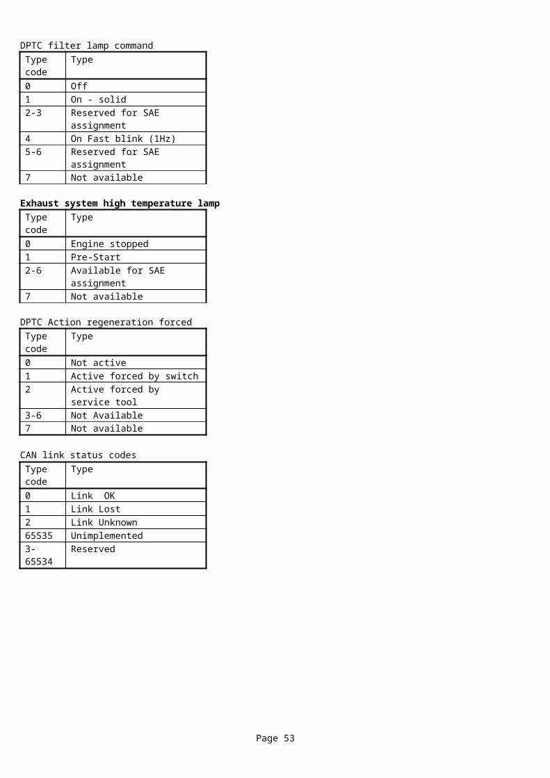
10.17 Page 17 - J1939 active diagnostic trouble codes in decoded format Notes:1. These are read only registers.2. Some Engine Control Units (ECUs) do not comply with J1939 with respect to trouble codes, the trouble code type must be read to
determine the interpretation of the codes.3. For an ECU that is fully compliant with J1939 this page contains the status as indicated by the last DM1 message, refer to J1939-73
section 5.7.1.4. For an ECU that is not fully compliant with J1939 this page contains trouble codes as read by the mechanism appropriate to the
ECU.5. The meaning of the lamp status codes is shown in the table below.6. For details of the Suspect Parameter Number (SPN) refer to J1939-04 Appendix C.7. For details of the Failure Mode Indicator (FMI) refer to J1939-73 Appendix A.8. For details of the Occurrence Count (OC) refer to J1939-73 section 5.7.1, a value of 127 indicates that no OC is available.9. For details of the Fault Code Number, Status of Fault Code and Number of Occurrences refer to the Scania document 'Fault codes
EMS S6'.10. For details of the Fault Code Number refer to the MTU document “Part 3 Maintenance and repair E531 711 / 01 E”
RegistersRegister offset
Name Minimum value
Maximum value
Scaling factor
Units Bits/ Sign
0 Number of active trouble codes 0 63 161 Malfunction indicator lamp status 0 3 15/16-16/16
Red stop lamp status 0 3 13/16-14/16Amber warning lamp status 0 3 11/16-12/16Protect lamp status 0 3 9/16-10/16Reserved for SAE assignment 0 3 7/16-8/16Reserved for SAE assignment 0 3 5/16-6/16Reserved for SAE assignment 0 3 3/16-4/16Reserved for SAE assignment 0 3 1/16-2/16
2-6 Trouble code 1 807-11 Trouble code 2 8012-16 Trouble code 3 8017-21 Trouble code 4 8022-246 Trouble codes 5-49247-251 Trouble code 50 80
Lamp status codesCode System control function0 Lamp off1 Lamp on2 Undefined3 Unimplemented
Trouble code typeCode Format0 J19391 Scania Keyword 2000 (KW2K)2 MTU3 Cummins Modbus4-99 Reserved
Page 53
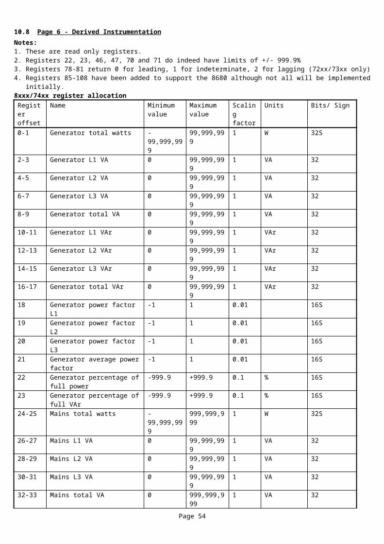
J1939 type trouble codeRegister offset
Name Minimum value
Maximum value
Scaling factor
Units Bits/ Sign
0--1 SPN 0 524287 322 FMI 0 31 163 OC 0 127 164 Trouble code type 0 0 16
Scania Keyword 2000 (KW2K) type trouble codeRegister offset
Name Minimum value
Maximum value
Scaling factor
Units Bits/ Sign
0-1 Fault code Number 0 65535 322 Status of Fault Code 0 255 163 Number of Occurrences 0 255 164 Trouble code type 1 1 16
MTU type trouble codeRegister offset
Name Minimum value
Maximum value
Scaling factor
Units Bits/ Sign
0-1 Fault code Number 0 400 322 Status of Fault Code 0 255 163 Number of Occurrences 0 255 164 Trouble code type 2 2 16
Page 54
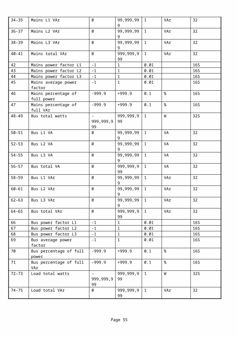
10.18 Page 18 - J1939 active diagnostic trouble codes in raw format Notes:1. These are read only registers.2. This page contains the status as indicated by the last DM1 message, refer to J1939-73 section 5.7.1.3. The meaning of the lamp status codes is shown in the table below.4. For details of the Suspect Parameter Number (SPN) refer to J1939-04 Appendix C.5. For details of the Failure Mode Indicator (FMI) refer to J1939-73 Appendix A.6. For details of the Occurrence Count (OC) refer to J1939-73 section 5.7.1, a value of 127 indicates that no OC is available.7. For details of the Conversion Method (CM) refer to J1939-73 section 5.7.1
RegistersRegister offset
Name Minimum value
Maximum value
Scaling factor
Units Bits/ Sign
0 Number of active trouble codes 0 126 161 Reserved 0 0 162 Reserved 0 0 163 Reserved for SAE assignment 0 3 15/16-16/16
Reserved for SAE assignment 0 3 13/16-14/16Reserved for SAE assignment 0 3 11/16-12/16Reserved for SAE assignment 0 3 9/16-10/16Protect lamp status 0 3 7/16-8/16Amber warning lamp status 0 3 5/16-6/16Red stop lamp status 0 3 3/16-4/16Malfunction indicator lamp status 0 3 1/16-2/16
4 Trouble code 1: Least significant 16 bits of SPN
0 65535 16
5 Trouble code 1: CM 0 1 16/16Trouble code 1: OC 0 127 9/16-15/16Trouble code 1: FMI 0 31 4/16-8/16Trouble code 1: Most significant 3 bits of SPN
0 7 1/16-3/16
6-7 Trouble code 2 as above 8-9 Trouble code 3 as above 10-255 Trouble codes 4-126 as above
Lamp status codesCode System control function0 Lamp off1 Lamp on2 Undefined3 Unimplemented
Page 55
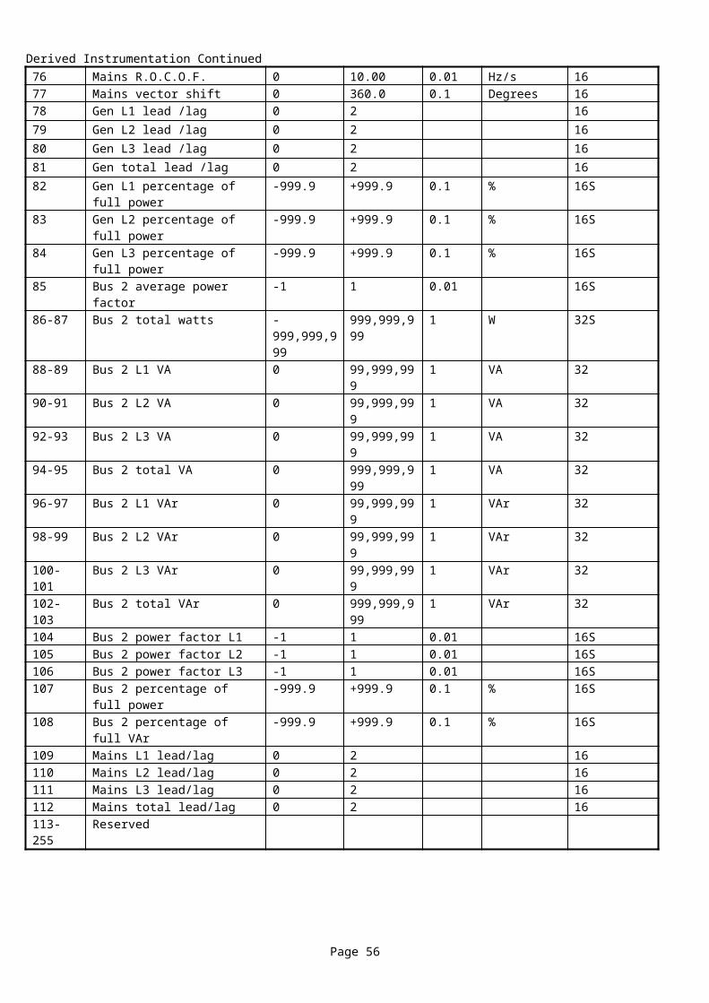
10.19 Page 20 - Various Strings Notes:1. These are read only registers.2. Each string consists of 32 Unicode characters with the first character at the lowest register address, NULL terminators are not used.3. The manufacturer string and model string must not be used to identify a particular product as they may change from one unit to the
next, e.g. a manufacturer may change its name in some way.4. The remaining strings can be used in a status display.5. The contents of these strings will never change while the slave device is operating so a copy can be held by the master to minimise
traffic.
RegistersRegister offset
Name Minimum value
Maximum value
Bits
0 Manufacturer string UNICODE UNICODE 51232 Model string UNICODE UNICODE 51264 Control unit not configured string UNICODE UNICODE 51296 Module variant UNICODE UNICODE 512128 Control unit failure string UNICODE UNICODE 512160 Shutdown alarm string UNICODE UNICODE 512192 Electrical trip alarm string UNICODE UNICODE 512224 Warning alarm string UNICODE UNICODE 512
10.20 Page 22- Auxiliary sender strings Notes:1. These are read only registers.2. Each string consists of 32 Unicode characters with the first character at the lowest register address, NULL terminators are not used.3. The strings can be used in a status display.4. The contents of these strings will never change while the slave device is operating so a copy can be held by the master to minimise
traffic.5. Reading the string for an unimplemented sender will return 32 spaces (Unicode 0x0020).
RegistersRegister offset
Name Minimum value
Maximum value
Bits
0 Auxiliary sender 1 string UNICODE UNICODE 51232 Auxiliary sender 2 string UNICODE UNICODE 51264 Auxiliary sender 3 string UNICODE UNICODE 51296 Auxiliary sender 4 string UNICODE UNICODE 512128-255 Reserved UNICODE UNICODE 512
10.21 Page 24 - Identity Strings Notes:1. These may be read/write or read only registers depending on the product.2. Each string consists of 32 Unicode characters with the first character at the lowest register address, NULL terminators are not used.3. The strings are user defined but are intended to allow the site and unit to be identified.4. The contents of these strings will never change while the slave device is operating so a copy can be held by the master to minimise
traffic.
RegistersRegister offset
Name Minimum value
Maximum value
Bits
0 Identity string 1 UNICODE UNICODE 51232 Identity string 2 UNICODE UNICODE 51264 Identity string 3 UNICODE UNICODE 51296 Identity string 4 UNICODE UNICODE 512128 Identity string 5 UNICODE UNICODE 512160 Identity string 6 UNICODE UNICODE 512192 Identity string 7 UNICODE UNICODE 512224 Identity string 8 UNICODE UNICODE 512
Page 56

10.22 Page 26 - State Machine Name Strings Notes:1. These are read only registers.2. Each string consists of 32 Unicode characters with the first character at the lowest register address, NULL terminators are not used.3. The strings contain the names of the state machines that are implemented in a particular slave device.4. The contents of these strings will never change while the slave device is operating so a copy can be held by the master to minimise
traffic.5. Reading the string for a unimplemented state machine will return 32 spaces (Unicode 0x0020).
RegistersRegister offset
Name Minimum value
Maximum value
Bits
0 S.M. 1 name string UNICODE UNICODE 51232 S.M. 2 name string UNICODE UNICODE 51264 S.M. 3 name string UNICODE UNICODE 51296 S.M. 4 name string UNICODE UNICODE 512128 S.M. 5 name string UNICODE UNICODE 512160 S.M. 6 name string UNICODE UNICODE 512192 S.M. 7 name string UNICODE UNICODE 512224 S.M. 8 name string UNICODE UNICODE 512
10.23 Page 28 - State Machine State Strings Notes:1. These are read only registers.2. Each string consists of 32 Unicode characters with the first character at the lowest register address, NULL terminators are not used.3. The contents of these strings may change at any time when the corresponding state machine changes state, refer to the ‘generating set
status information’ page for details.4. A complete string must be read with a single query to avoid the possibility of reading parts from different strings, any attempt to read
part of a string will return extended exception 13 (Block violation).5. Up to 3 complete consecutive strings can be read with a single query, limited only by the packet size limitations of Modbus.6. Reading a string causes the corresponding state machine status code in the ‘generating set status information’ page to change to 0.7. A string can be read regardless of the state machine status code.8. Reading the string for a unimplemented state machine will return 32 spaces (Unicode 0x0020).9. This page is not implemented on the 72xx/73xx and 8xxx/74xx families.
RegistersRegister offset
Name Minimum value
Maximum value
Bits
0 S.M. 1 state string UNICODE UNICODE 51232 S.M. 2 state string UNICODE UNICODE 51264 S.M. 3 state string UNICODE UNICODE 51296 S.M. 4 state string UNICODE UNICODE 512128 S.M. 5 state string UNICODE UNICODE 512160 S.M. 6 state string UNICODE UNICODE 512192 S.M. 7 state string UNICODE UNICODE 512224 S.M. 8 state string UNICODE UNICODE 512
Page 57
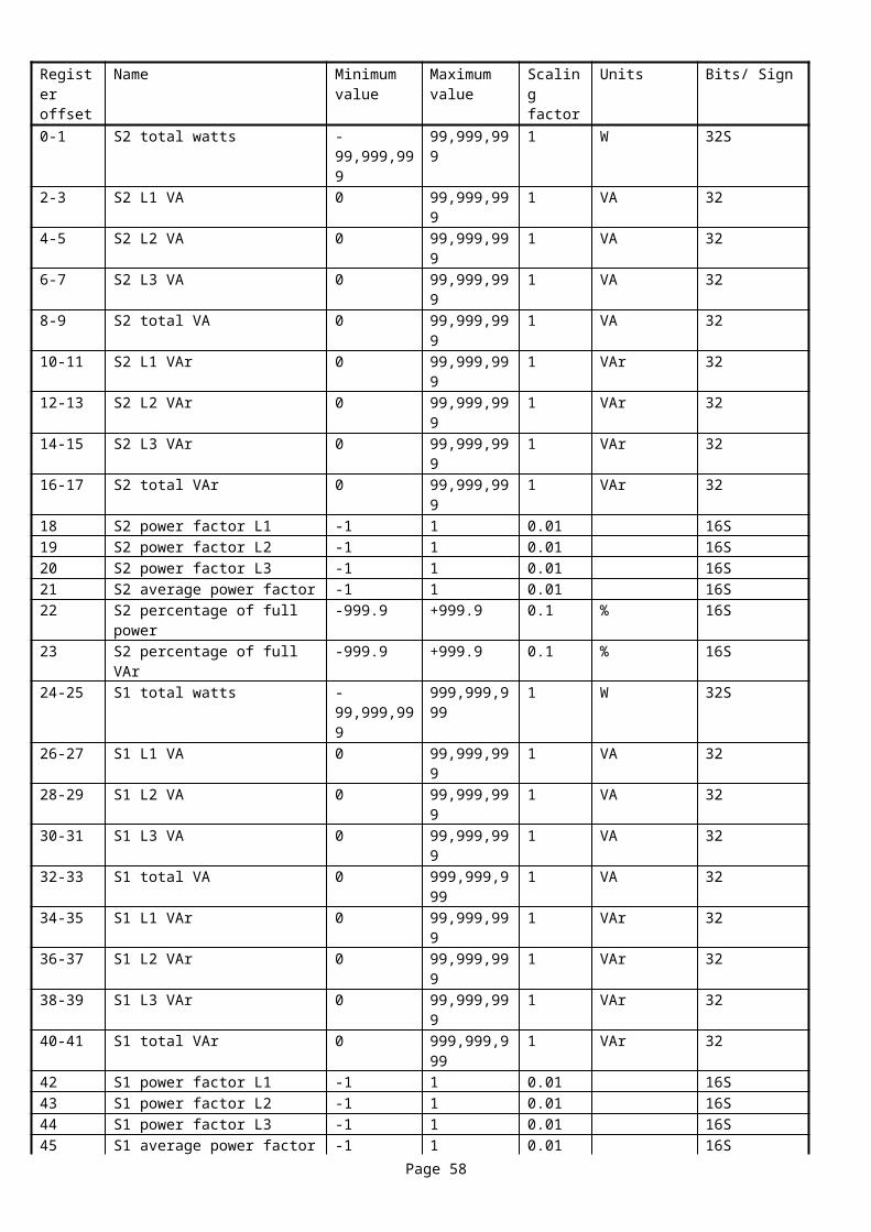
10.24 Pages 32 to 95 - Alarm Strings (Old alarm system) Notes:1. These are read only registers.2. Each string consists of 32 Unicode characters with the first character at the lowest register address, NULL terminators are not used.3. There are 2 strings corresponding to each alarm, refer to the alarm conditions page for details of their use.4. The contents of these strings will never change while the slave device is operating so a copy can be held by the master to minimise
traffic.5. Reading the string for an unimplemented alarm will return 32 spaces (Unicode 0x0020).6. The inactive string for an alarm may not be used, in which case it will return 32 spaces (Unicode 0x0020).7. The old alarm system is not implemented on the 72xx/73xx and 8xxx/74xx families.
RegistersPage Register
offsetName Minimum
valueMaximum value
Bits
32 0 Emergency stop inactive string UNICODE UNICODE 51232 Emergency stop active string UNICODE UNICODE 51264 Low oil pressure inactive string UNICODE UNICODE 51296 Low oil pressure active string UNICODE UNICODE 512128 High coolant temperature inactive string UNICODE UNICODE 512160 High coolant temperature active string UNICODE UNICODE 512192 High oil temperature inactive string UNICODE UNICODE 512224 High oil temperature active string UNICODE UNICODE 512
33 0 Under speed inactive string UNICODE UNICODE 51232 Under speed active string UNICODE UNICODE 51264 Over speed inactive string UNICODE UNICODE 51296 Over speed active string UNICODE UNICODE 512128 Fail to start inactive string UNICODE UNICODE 512160 Fail to start active string UNICODE UNICODE 512192 Fail to come to rest inactive string UNICODE UNICODE 512224 Fail to come to rest active string UNICODE UNICODE 512
34 0 Loss of speed sensing inactive string UNICODE UNICODE 51232 Loss of speed sensing active string UNICODE UNICODE 51264 Generator low voltage inactive string UNICODE UNICODE 51296 Generator low voltage active string UNICODE UNICODE 512128 Generator high voltage inactive string UNICODE UNICODE 512160 Generator high voltage active string UNICODE UNICODE 512192 Generator low frequency inactive string UNICODE UNICODE 512224 Generator low frequency active string UNICODE UNICODE 512
35 0 Generator high frequency inactive string UNICODE UNICODE 51232 Generator high frequency active string UNICODE UNICODE 51264 Generator high current inactive string UNICODE UNICODE 51296 Generator high current active string UNICODE UNICODE 512128 Generator earth fault inactive string UNICODE UNICODE 512160 Generator earth fault active string UNICODE UNICODE 512192 Generator reverse power inactive string UNICODE UNICODE 512224 Generator reverse power active string UNICODE UNICODE 512
36 0 Air flap inactive string UNICODE UNICODE 51232 Air flap active string UNICODE UNICODE 51264 Oil pressure sender fault inactive string UNICODE UNICODE 51296 Oil pressure sender fault active string UNICODE UNICODE 512128 Coolant temperature sender fault inactive string UNICODE UNICODE 512160 Coolant temperature sender fault active string UNICODE UNICODE 512192 Oil temperature sender fault inactive string UNICODE UNICODE 512224 Oil temperature sender fault active string UNICODE UNICODE 512
Page 58
Alarm strings continuedPage Register
offsetName Minimum
valueMaximum value
Bits
37 0 Fuel level sender fault inactive string UNICODE UNICODE 51232 Fuel level sender fault active string UNICODE UNICODE 51264 Magnetic pickup fault inactive string UNICODE UNICODE 51296 Magnetic pickup fault active string UNICODE UNICODE 512128 Loss of AC speed signal inactive string UNICODE UNICODE 512160 Loss of AC speed signal active string UNICODE UNICODE 512192 Charge alternator failure inactive string UNICODE UNICODE 512224 Charge alternator failure active string UNICODE UNICODE 512
38 0 Low battery voltage inactive string UNICODE UNICODE 51232 Low battery voltage active string UNICODE UNICODE 51264 High battery voltage inactive string UNICODE UNICODE 51296 High battery voltage active string UNICODE UNICODE 512128 Low fuel level inactive string UNICODE UNICODE 512160 Low fuel level active string UNICODE UNICODE 512192 High fuel level inactive string UNICODE UNICODE 512224 High fuel level active string UNICODE UNICODE 512
39 0 Generator failed to close inactive string UNICODE UNICODE 51232 Generator failed to close active string UNICODE UNICODE 51264 Mains failed to close inactive string UNICODE UNICODE 51296 Mains failed to close active string UNICODE UNICODE 512128 Generator failed to open inactive string UNICODE UNICODE 512160 Generator failed to open active string UNICODE UNICODE 512192 Mains failed to open inactive string UNICODE UNICODE 512224 Mains failed to open active string UNICODE UNICODE 512
40 0 Mains low voltage inactive string UNICODE UNICODE 51232 Mains low voltage active string UNICODE UNICODE 51264 Mains high voltage inactive string UNICODE UNICODE 51296 Mains high voltage active string UNICODE UNICODE 512128 Bus failed to close inactive string UNICODE UNICODE 512160 Bus failed to close active string UNICODE UNICODE 512192 Bus failed to open inactive string UNICODE UNICODE 512224 Bus failed to open active string UNICODE UNICODE 512
41 0 Mains low frequency inactive string UNICODE UNICODE 51232 Mains low frequency active string UNICODE UNICODE 51264 Mains high frequency inactive string UNICODE UNICODE 51296 Mains high frequency active string UNICODE UNICODE 512128 Mains failed inactive string UNICODE UNICODE 512160 Mains failed active string UNICODE UNICODE 512192 Mains phase rotation wrong inactive string UNICODE UNICODE 512224 Mains phase rotation wrong active string UNICODE UNICODE 512
42 0 Generator phase rotation wrong inactive string UNICODE UNICODE 51232 Generator phase rotation wrong active string UNICODE UNICODE 51264 Maintenance due inactive string UNICODE UNICODE 51296 Maintenance due active string UNICODE UNICODE 512128 Clock not set inactive string UNICODE UNICODE 512160 Clock not set active string UNICODE UNICODE 512192 Local LCD configuration lost inactive string UNICODE UNICODE 512224 Local LCD configuration lost inactive string UNICODE UNICODE 512
Page 59
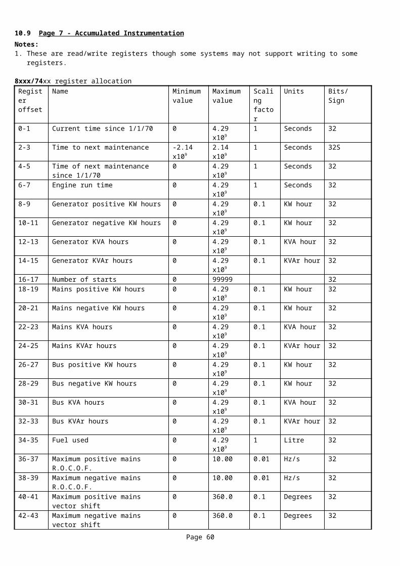
Alarm strings continuedPage Register
offsetName Minimum
valueMaximum value
Bits
43 0 Local telemetry configuration lost inactive string UNICODE UNICODE 51232 Local telemetry configuration lost active string UNICODE UNICODE 51264 Calibration lost inactive string UNICODE UNICODE 51296 Calibration lost active string UNICODE UNICODE 512128 Modem power fault inactive string UNICODE UNICODE 512160 Modem power fault active string UNICODE UNICODE 512192 Generator short circuit inactive string UNICODE UNICODE 512224 Generator short circuit active string UNICODE UNICODE 512
44 0 Failure to synchronise inactive string UNICODE UNICODE 51232 Failure to synchronise active string UNICODE UNICODE 51264 Bus live inactive string UNICODE UNICODE 51296 Bus live active string UNICODE UNICODE 512128 Scheduled run inactive string UNICODE UNICODE 512160 Scheduled run active string UNICODE UNICODE 512192 Bus phase rotation wrong inactive string UNICODE UNICODE 512224 Bus phase rotation wrong active string UNICODE UNICODE 512
45 0 Priority selection error inactive string UNICODE UNICODE 51232 Priority selection error active string UNICODE UNICODE 51264 MSC data error inactive string UNICODE UNICODE 51296 MSC data error active string UNICODE UNICODE 512128 MSC ID error inactive string UNICODE UNICODE 512160 MSC ID error active string UNICODE UNICODE 512192 MSC failure inactive string UNICODE UNICODE 512224 MSC failure active string UNICODE UNICODE 512
46 0 MSC too few sets inactive string UNICODE UNICODE 51232 MSC too few sets active string UNICODE UNICODE 51264 MSC alarms inhibited inactive string UNICODE UNICODE 51296 MSC alarms inhibited active string UNICODE UNICODE 512128 MSC old version units inactive string UNICODE UNICODE 512160 MSC old version units active string UNICODE UNICODE 512192 Mains reverse power inactive string UNICODE UNICODE 512224 Mains reverse power active string UNICODE UNICODE 512
47 0 Minimum sets not reached inactive string UNICODE UNICODE 51232 Minimum sets not reached active string UNICODE UNICODE 51264 Insufficient capacity available inactive string UNICODE UNICODE 51296 Insufficient capacity available active string UNICODE UNICODE 512128 Expansion input unit not calibrated inactive string UNICODE UNICODE 512160 Expansion input unit not calibrated active string UNICODE UNICODE 512192 Expansion input unit failure inactive string UNICODE UNICODE 512224 Expansion input unit failure active string UNICODE UNICODE 512
Page 60
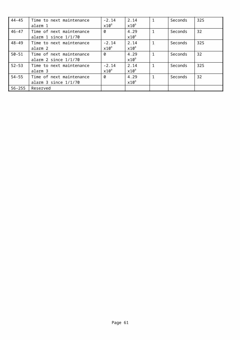
Alarm strings continuedPage Register
offsetName Minimum
valueMaximum value
Bits
48 0 Auxiliary sender 1 low inactive string UNICODE UNICODE 51232 Auxiliary sender 1 low active string UNICODE UNICODE 51264 Auxiliary sender 1 high inactive string UNICODE UNICODE 51296 Auxiliary sender 1 high active string UNICODE UNICODE 512128 Auxiliary sender 1 fault inactive string UNICODE UNICODE 512160 Auxiliary sender 1 fault active string UNICODE UNICODE 512192 Auxiliary sender 2 low inactive string UNICODE UNICODE 512224 Auxiliary sender 2 low active string UNICODE UNICODE 512
49 0 Auxiliary sender 2 high inactive string UNICODE UNICODE 51232 Auxiliary sender 2 high active string UNICODE UNICODE 51264 Auxiliary sender 2 fault inactive string UNICODE UNICODE 51296 Auxiliary sender 2 fault active string UNICODE UNICODE 512128 Auxiliary sender 3 low inactive string UNICODE UNICODE 512160 Auxiliary sender 3 low active string UNICODE UNICODE 512192 Auxiliary sender 3 high inactive string UNICODE UNICODE 512224 Auxiliary sender 3 high active string UNICODE UNICODE 512
50 0 Auxiliary sender 3 fault inactive string UNICODE UNICODE 51232 Auxiliary sender 3 fault active string UNICODE UNICODE 51264 Auxiliary sender 4 low inactive string UNICODE UNICODE 51296 Auxiliary sender 4 low active string UNICODE UNICODE 512128 Auxiliary sender 4 high inactive string UNICODE UNICODE 512160 Auxiliary sender 4 high active string UNICODE UNICODE 512192 Auxiliary sender 4 high inactive string UNICODE UNICODE 512224 Auxiliary sender 4 high active string UNICODE UNICODE 512
51 0 Engine control unit (ECU) link lost inactive string UNICODE UNICODE 51232 Engine control unit (ECU) link lost active string UNICODE UNICODE 51264 Engine control unit (ECU) failure inactive string UNICODE UNICODE 51296 Engine control unit (ECU) failure active string UNICODE UNICODE 512128 Engine control unit (ECU) error inactive string UNICODE UNICODE 512160 Engine control unit (ECU) error active string UNICODE UNICODE 512192 Low coolant temperature inactive string UNICODE UNICODE 512224 Low coolant temperature active string UNICODE UNICODE 512
52 0 Out of sync inactive string UNICODE UNICODE 51232 Out of sync active string UNICODE UNICODE 51264 Low Oil Pressure Switch inactive string UNICODE UNICODE 51296 Low Oil Pressure Switch active string UNICODE UNICODE 512128 Alternative Aux Mains Fail inactive string UNICODE UNICODE 512160 Alternative Aux Mains Fail active string UNICODE UNICODE 512192 Loss of excitation inactive string UNICODE UNICODE 512224 Loss of excitation active string UNICODE UNICODE 512
Page 61
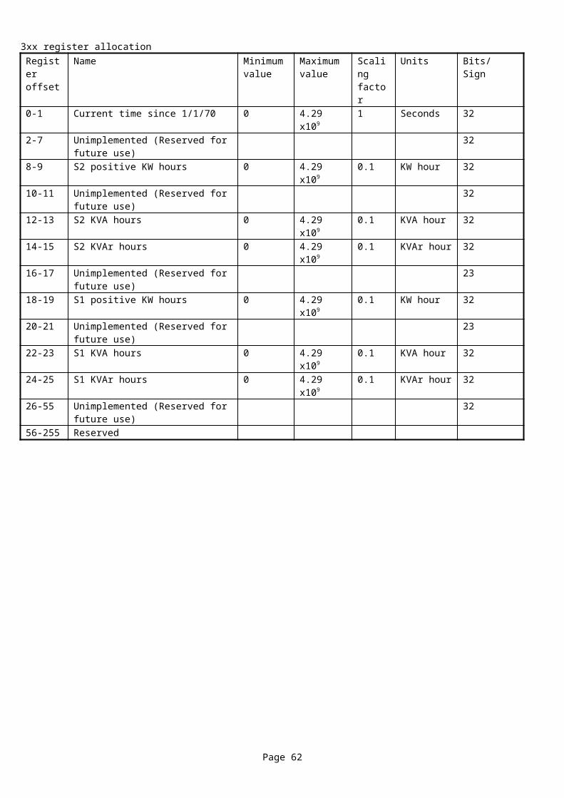
Alarm strings continuedPage Register
offsetName Minimum
valueMaximum value
Bits
53 0 Mains kW Limit inactive string UNICODE UNICODE 51232 Mains kW Limit active string UNICODE UNICODE 51264 Negative phase sequence inactive string UNICODE UNICODE 51296 Negative phase sequence active string UNICODE UNICODE 512128 Mains ROCOF inactive string UNICODE UNICODE 512160 Mains ROCOF active string UNICODE UNICODE 512192 Mains vector shift inactive string UNICODE UNICODE 512224 Mains vector shift active string UNICODE UNICODE 512
54 0 Mains G59 low frequency inactive string UNICODE UNICODE 51232 Mains G59 low frequency active string UNICODE UNICODE 51264 Mains G59 high frequency inactive string UNICODE UNICODE 51296 Mains G59 high frequency active string UNICODE UNICODE 512128 Mains G59 low voltage inactive string UNICODE UNICODE 512160 Mains G59 low voltage active string UNICODE UNICODE 512192 Mains G59 high voltage inactive string UNICODE UNICODE 512224 Mains G59 high voltage active string UNICODE UNICODE 512
55 0 Mains G59 trip inactive string UNICODE UNICODE 51232 Mains G59 trip active string UNICODE UNICODE 51264 Generator kW Overload inactive string UNICODE UNICODE 51296 Generator kW Overload active string UNICODE UNICODE 512128 Engine Inlet Temp High inactive string UNICODE UNICODE 512160 Engine Inlet Temp High inactive string UNICODE UNICODE 512192 Bus 1 live inactive string UNICODE UNICODE 512224 Bus 1 live active string UNICODE UNICODE 512
56 0 Bus 1 phase rotation wrong inactive string UNICODE UNICODE 51232 Bus 1 phase rotation wrong active string UNICODE UNICODE 51264 Bus 2 live inactive string UNICODE UNICODE 51296 Bus 2 live active string UNICODE UNICODE 512128 Bus 2 phase rotation wrong inactive string UNICODE UNICODE 512160 Bus 2 phase rotation wrong active string UNICODE UNICODE 512192 Reserved UNICODE UNICODE 512224 Reserved UNICODE UNICODE 512
57-63 Reserved
Page 62

Alarm strings continuedPage Register
offsetName Minimum
valueMaximum value
Bits
64 0 Unnamed digital input 1 inactive string UNICODE UNICODE 51232 Unnamed digital input 1 active string UNICODE UNICODE 51264 Unnamed digital input 2 inactive string UNICODE UNICODE 51296 Unnamed digital input 2 active string UNICODE UNICODE 512128 Unnamed digital input 3 inactive string UNICODE UNICODE 512160 Unnamed digital input 3 active string UNICODE UNICODE 512192 Unnamed digital input 4 inactive string UNICODE UNICODE 512224 Unnamed digital input 4 active string UNICODE UNICODE 512
65 Unnamed digital input 5-8 strings66 Unnamed digital input 9-12 strings67 Unnamed digital input 13-16 strings68 Unnamed digital input 17-20 strings69 Unnamed digital input 21-24 strings70 Unnamed digital input 25-28 strings71 Unnamed digital input 29-32 strings72 Unnamed digital input 33-36 strings73 Unnamed digital input 37-40 strings74 Unnamed digital input 41-44 strings75 Unnamed digital input 45-48 strings76 Unnamed digital input 49-52 strings77 Unnamed digital input 53-56 strings78 Unnamed digital input 57-60 strings79 Unnamed digital input 61-64 strings80 Unnamed digital input 65-68 strings81 Unnamed digital input 69-72 strings82 Unnamed digital input 73-76 strings83 Unnamed digital input 77-80 strings84 Unnamed digital input 81-84 strings85 Unnamed digital input 85-88 strings86 Unnamed digital input 89-92 strings87 Unnamed digital input 93-96 strings88 Unnamed digital input 97-100 strings89 Unnamed digital input 101-104 strings90 Unnamed digital input 105-108 strings91 Unnamed digital input 109-112 strings92 Unnamed digital input 113-116 strings93 Unnamed digital input 117-120 strings94 Unnamed digital input 121-124 strings95 Unnamed digital input 125-128 strings
Page 63
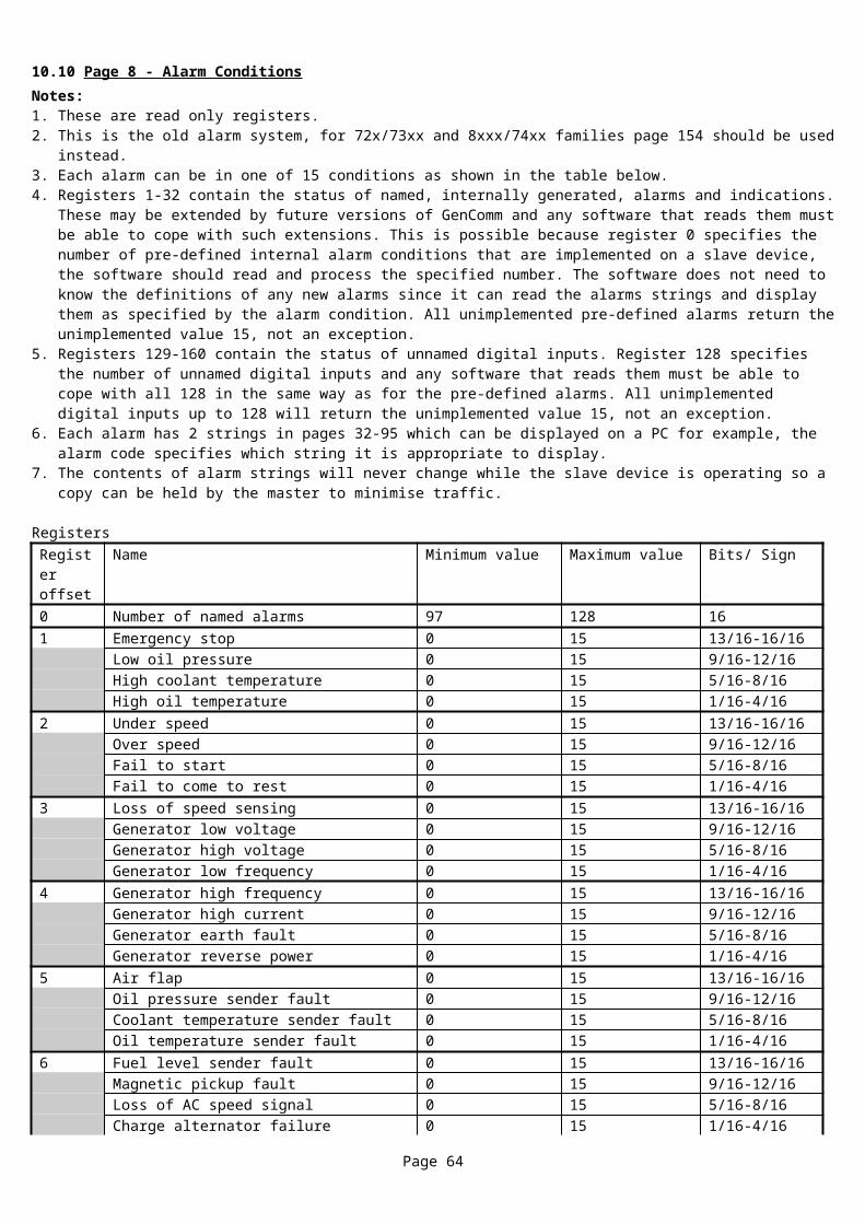
10.25 Pages 32-36 - 2131 Expansion module name strings 1. These registers provide the user defined names of each channel of each expansion module.2. These pages are implemented on the 72xx/73xx, 8xxx/74xx and later families and replace the alarm strings from the old alarm
system.
32 0 2131 Expansion module 0 input A name string UNICODE UNICODE 51232 2131 Expansion module 0 input B name string UNICODE UNICODE 51264 2131 Expansion module 0 input C name string UNICODE UNICODE 51296 2131 Expansion module 0 input D name string UNICODE UNICODE 512128 2131 Expansion module 0 input E name string UNICODE UNICODE 512160 2131 Expansion module 0 input F name string UNICODE UNICODE 512192 2131 Expansion module 0 input G name string UNICODE UNICODE 512224 2131 Expansion module 0 input H name string UNICODE UNICODE 512
33 0 2131 Expansion module 0 input I name string UNICODE UNICODE 51232 2131 Expansion module 0 input J name string UNICODE UNICODE 51264 2131 Expansion module 1 input A name string UNICODE UNICODE 51296 2131 Expansion module 1 input B name string UNICODE UNICODE 512128 2131 Expansion module 1 input C name string UNICODE UNICODE 512160 2131 Expansion module 1 input D name string UNICODE UNICODE 512192 2131 Expansion module 1 input E name string UNICODE UNICODE 512224 2131 Expansion module 1 input F name string UNICODE UNICODE 512
34 0 2131 Expansion module 1 input G name string UNICODE UNICODE 51232 2131 Expansion module 1 input H name string UNICODE UNICODE 51264 2131 Expansion module 1 input I name string UNICODE UNICODE 51296 2131 Expansion module 1 input J name string UNICODE UNICODE 512128 2131 Expansion module 2 input A name string UNICODE UNICODE 512160 2131 Expansion module 2 input B name string UNICODE UNICODE 512192 2131 Expansion module 2 input C name string UNICODE UNICODE 512224 2131 Expansion module 2 input D name string UNICODE UNICODE 512
35 0 2131 Expansion module 2 input E name string UNICODE UNICODE 51232 2131 Expansion module 2 input F name string UNICODE UNICODE 51264 2131 Expansion module 2 input G name string UNICODE UNICODE 51296 2131 Expansion module 2 input H name string UNICODE UNICODE 512128 2131 Expansion module 2 input I name string UNICODE UNICODE 512160 2131 Expansion module 2 input J name string UNICODE UNICODE 512192 2131 Expansion module 3 input A name string UNICODE UNICODE 512224 2131 Expansion module 3 input B name string UNICODE UNICODE 512
36 0 2131 Expansion module 3 input C name string UNICODE UNICODE 51232 2131 Expansion module 3 input D name string UNICODE UNICODE 51264 2131 Expansion module 3 input E name string UNICODE UNICODE 51296 2131 Expansion module 3 input F name string UNICODE UNICODE 512128 2131 Expansion module 3 input G name string UNICODE UNICODE 512160 2131 Expansion module 3 input H name string UNICODE UNICODE 512192 2131 Expansion module 3 input I name string UNICODE UNICODE 512224 2131 Expansion module 3 input J name string UNICODE UNICODE 512
Page 64
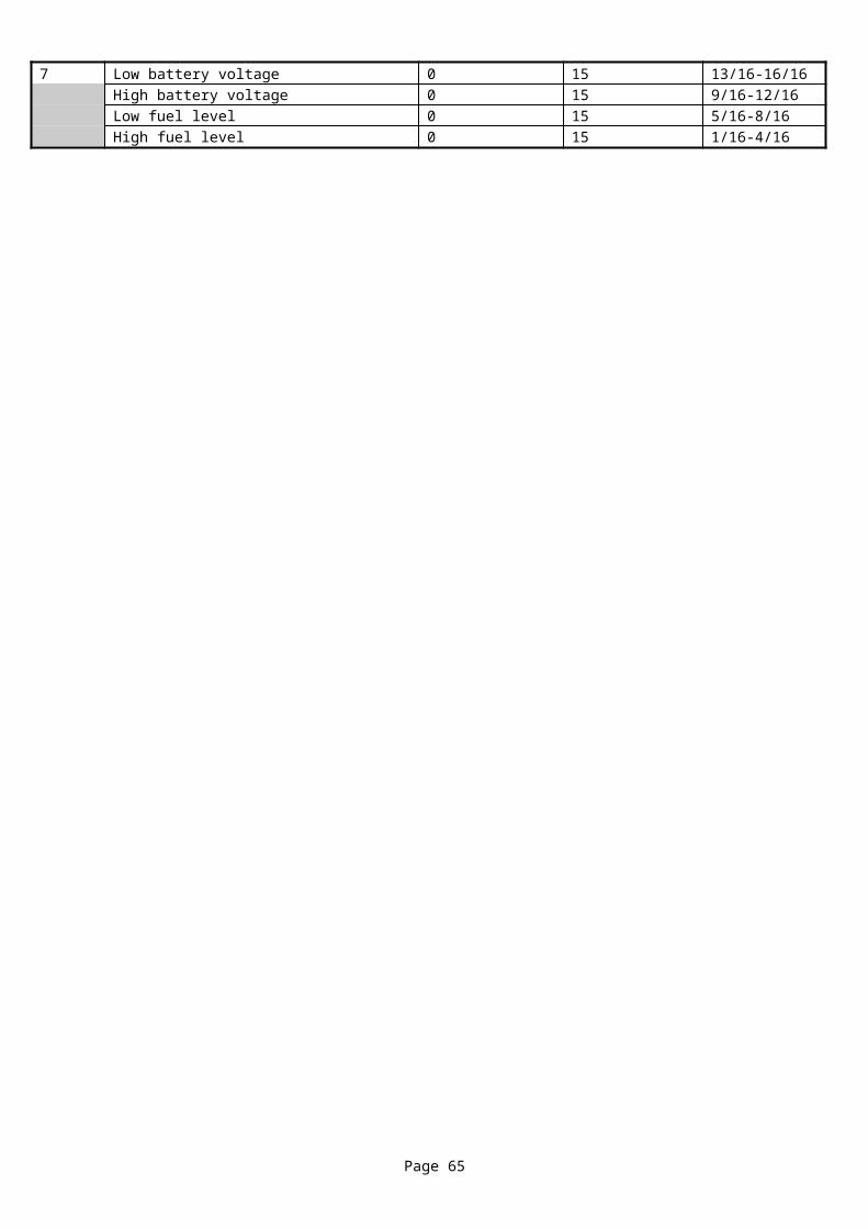
10.26 Pages 37-40 - 2133 Expansion module name strings 1. These registers provide the user defined names of each channel of each expansion module.2. These pages are implemented on the 72xx/73xx, 8xxx/74xx and later families and replace the alarm strings from the old alarm
system.
37 0 2133 Expansion module 0 input A name string UNICODE UNICODE 51232 2133 Expansion module 0 input B name string UNICODE UNICODE 51264 2133 Expansion module 0 input C name string UNICODE UNICODE 51296 2133 Expansion module 0 input D name string UNICODE UNICODE 512128 2133 Expansion module 0 input E name string UNICODE UNICODE 512160 2133 Expansion module 0 input F name string UNICODE UNICODE 512192 2133 Expansion module 0 input G name string UNICODE UNICODE 512224 2133 Expansion module 0 input H name string UNICODE UNICODE 512
38 0 2133 Expansion module 1 input A name string UNICODE UNICODE 51232 2133 Expansion module 1 input B name string UNICODE UNICODE 51264 2133 Expansion module 1 input C name string UNICODE UNICODE 51296 2133 Expansion module 1 input D name string UNICODE UNICODE 512128 2133 Expansion module 1 input E name string UNICODE UNICODE 512160 2133 Expansion module 1 input F name string UNICODE UNICODE 512192 2133 Expansion module 1 input G name string UNICODE UNICODE 512224 2133 Expansion module 2 input G name string UNICODE UNICODE 512
39 0 2133 Expansion module 2 input A name string UNICODE UNICODE 51232 2133 Expansion module 2 input B name string UNICODE UNICODE 51264 2133 Expansion module 2 input C name string UNICODE UNICODE 51296 2133 Expansion module 2 input D name string UNICODE UNICODE 512128 2133 Expansion module 2 input E name string UNICODE UNICODE 512160 2133 Expansion module 2 input F name string UNICODE UNICODE 512192 2133 Expansion module 2 input G name string UNICODE UNICODE 512224 2133 Expansion module 2 input H name string UNICODE UNICODE 512
40 0 2133 Expansion module 3 input A name string UNICODE UNICODE 51232 2133 Expansion module 3 input B name string UNICODE UNICODE 51264 2133 Expansion module 3 input C name string UNICODE UNICODE 51296 2133 Expansion module 3 input D name string UNICODE UNICODE 512128 2133 Expansion module 3 input E name string UNICODE UNICODE 512160 2133 Expansion module 3 input F name string UNICODE UNICODE 512192 2133 Expansion module 3 input G name string UNICODE UNICODE 512224 2133 Expansion module 3 input H name string UNICODE UNICODE 512
Page 65
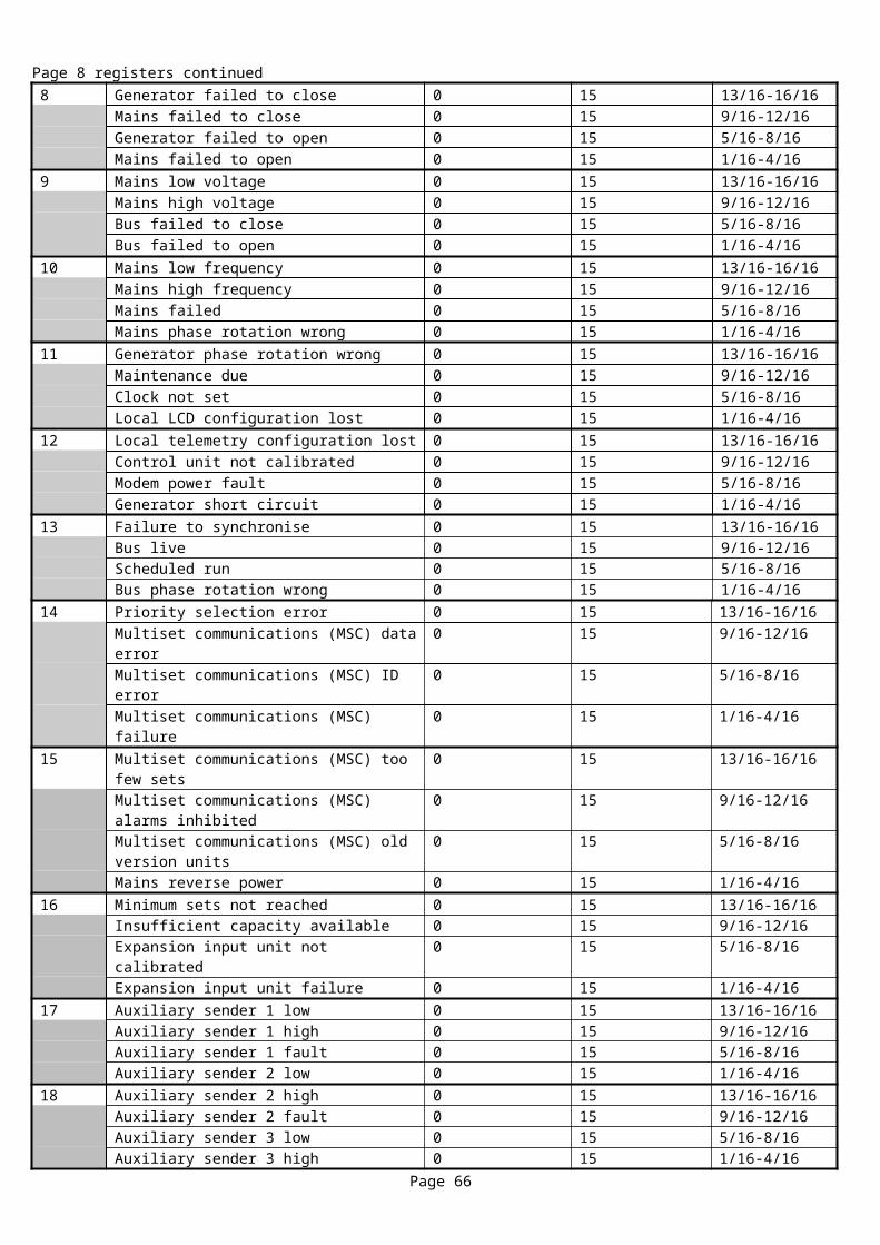
10.27 Pages 41-43 - 2152 Expansion module name strings 1. These registers provide the user defined names of each channel of each expansion module.2. These pages are implemented on the 72xx/73xx, 8xxx/74xx and later families and replace the alarm strings from the old alarm
system.
41 0 2152 Expansion module 0 input A name string UNICODE UNICODE 51232 2152 Expansion module 0 input B name string UNICODE UNICODE 51264 2152 Expansion module 0 input C name string UNICODE UNICODE 51296 2152 Expansion module 0 input D name string UNICODE UNICODE 512128 2152 Expansion module 0 input E name string UNICODE UNICODE 512160 2152 Expansion module 0 input F name string UNICODE UNICODE 512192 2152 Expansion module 1 input A name string UNICODE UNICODE 512224 2152 Expansion module 1 input B name string UNICODE UNICODE 512
42 0 2152 Expansion module 1 input C name string UNICODE UNICODE 51232 2152 Expansion module 1 input D name string UNICODE UNICODE 51264 2152 Expansion module 1 input E name string UNICODE UNICODE 51296 2152 Expansion module 1 input F name string UNICODE UNICODE 512128 2152 Expansion module 2 input A name string UNICODE UNICODE 512160 2152 Expansion module 2 input B name string UNICODE UNICODE 512192 2152 Expansion module 2 input C name string UNICODE UNICODE 512224 2152 Expansion module 2 input D name string UNICODE UNICODE 512
43 0 2152 Expansion module 2 input E name string UNICODE UNICODE 51232 2152 Expansion module 2 input F name string UNICODE UNICODE 51264 2152 Expansion module 3 input A name string UNICODE UNICODE 51296 2152 Expansion module 3 input B name string UNICODE UNICODE 512128 2152 Expansion module 3 input C name string UNICODE UNICODE 512160 2152 Expansion module 3 input D name string UNICODE UNICODE 512192 2152 Expansion module 3 input E name string UNICODE UNICODE 512224 2152 Expansion module 3 input F name string UNICODE UNICODE 512
Page 66
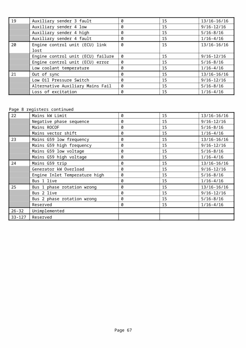
10.28 Pages 44-48 - 2131 Expansion module digital alarm strings 1. These registers provide the user defined alarm names of each channel of each expansion module when configured as a digital
input.2. These pages are implemented on the 72xx/73xx, 8xxx/74xx and later families and replace the alarm strings from the old alarm
system.
44 0 2131 Expansion module 0 digital input A string UNICODE UNICODE 51232 2131 Expansion module 0 digital input B string UNICODE UNICODE 51264 2131 Expansion module 0 digital input C string UNICODE UNICODE 51296 2131 Expansion module 0 digital input D string UNICODE UNICODE 512128 2131 Expansion module 0 digital input E string UNICODE UNICODE 512160 2131 Expansion module 0 digital input F string UNICODE UNICODE 512192 2131 Expansion module 0 digital input G String UNICODE UNICODE 512224 2131 Expansion module 0 digital input H string UNICODE UNICODE 512
45 0 2131 Expansion module 0 digital input I string UNICODE UNICODE 51232 2131 Expansion module 0 digital input J string UNICODE UNICODE 51264 2131 Expansion module 1 digital input A string UNICODE UNICODE 51296 2131 Expansion module 1 digital input B string UNICODE UNICODE 512128 2131 Expansion module 1 digital input C string UNICODE UNICODE 512160 2131 Expansion module 1 digital input D string UNICODE UNICODE 512192 2131 Expansion module 1 digital input E string UNICODE UNICODE 512224 2131 Expansion module 1 digital input F string UNICODE UNICODE 512
46 0 2131 Expansion module 1 digital input G string UNICODE UNICODE 51232 2131 Expansion module 1 digital input H string UNICODE UNICODE 51264 2131 Expansion module 1 digital input I string UNICODE UNICODE 51296 2131 Expansion module 1 digital input J string UNICODE UNICODE 512128 2131 Expansion module 2 digital input A string UNICODE UNICODE 512160 2131 Expansion module 2 digital input B string UNICODE UNICODE 512192 2131 Expansion module 2 digital input C string UNICODE UNICODE 512224 2131 Expansion module 2 digital input D string UNICODE UNICODE 512
47 0 2131 Expansion module 2 digital input E string UNICODE UNICODE 51232 2131 Expansion module 2 digital input F string UNICODE UNICODE 51264 2131 Expansion module 2 digital input G string UNICODE UNICODE 51296 2131 Expansion module 2 digital input H string UNICODE UNICODE 512128 2131 Expansion module 2 digital input I string UNICODE UNICODE 512160 2131 Expansion module 2 digital input J string UNICODE UNICODE 512192 2131 Expansion module 3 digital input A string UNICODE UNICODE 512224 2131 Expansion module 3 digital input B string UNICODE UNICODE 512
48 0 2131 Expansion module 3 digital input C string UNICODE UNICODE 51232 2131 Expansion module 3 digital input D string UNICODE UNICODE 51264 2131 Expansion module 3 digital input E string UNICODE UNICODE 51296 2131 Expansion module 3 digital input F string UNICODE UNICODE 512128 2131 Expansion module 3 digital input G string UNICODE UNICODE 512160 2131 Expansion module 3 digital input H string UNICODE UNICODE 512192 2131 Expansion module 3 digital input I string UNICODE UNICODE 512224 2131 Expansion module 3 digital input J string UNICODE UNICODE 512
Page 67
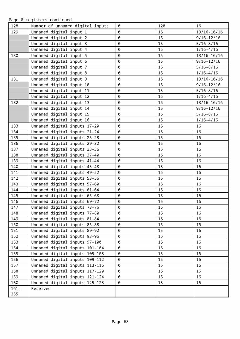
10.29 Pages 49-58 - 2131 Expansion module analogue alarm strings 1. These registers provide the user defined alarm names of each channel of each expansion module when configured as an
analogue input.2. These pages are implemented on the 72xx/73xx, 8xxx/74xx and later families and replace the alarm strings from the old alarm
system.
49 0 2131 Expansion module 0 input A (low) string UNICODE UNICODE 51232 2131 Expansion module 0 input A (high) string UNICODE UNICODE 51264 2131 Expansion module 0 input B (low) string UNICODE UNICODE 51296 2131 Expansion module 0 input B (high) string UNICODE UNICODE 512128 2131 Expansion module 0 input C (low) string UNICODE UNICODE 512160 2131 Expansion module 0 input C (high) string UNICODE UNICODE 512192 2131 Expansion module 0 input D (low) string UNICODE UNICODE 512224 2131 Expansion module 0 input D (high) string UNICODE UNICODE 512
50 0 2131 Expansion module 0 input E (low) string UNICODE UNICODE 51232 2131 Expansion module 0 input E (high) string UNICODE UNICODE 51264 2131 Expansion module 0 input F (low) string UNICODE UNICODE 51296 2131 Expansion module 0 input F (high) string UNICODE UNICODE 512128 2131 Expansion module 0 input G (low) string UNICODE UNICODE 512160 2131 Expansion module 0 input G (high) string UNICODE UNICODE 512192 2131 Expansion module 0 input H (low) string UNICODE UNICODE 512224 2131 Expansion module 0 input H (high) string UNICODE UNICODE 512
51 0 2131 Expansion module 0 input I (low) string UNICODE UNICODE 51232 2131 Expansion module 0 input I (high) string UNICODE UNICODE 51264 2131 Expansion module 0 input J (low) string UNICODE UNICODE 51296 2131 Expansion module 0 input J (high) string UNICODE UNICODE 512128 2131 Expansion module 1 input A (low) string UNICODE UNICODE 512160 2131 Expansion module 1 input A (high) string UNICODE UNICODE 512192 2131 Expansion module 1 input B (low) string UNICODE UNICODE 512224 2131 Expansion module 1 input B (high) string UNICODE UNICODE 512
52 0 2131 Expansion module 1 input C (low) string UNICODE UNICODE 51232 2131 Expansion module 1 input C (high) string UNICODE UNICODE 51264 2131 Expansion module 1 input D (low) string UNICODE UNICODE 51296 2131 Expansion module 1 input D (high) string UNICODE UNICODE 512128 2131 Expansion module 1 input E (low) string UNICODE UNICODE 512160 2131 Expansion module 1 input E (high) string UNICODE UNICODE 512192 2131 Expansion module 1 input F (low) string UNICODE UNICODE 512224 2131 Expansion module 1 input F (high) string UNICODE UNICODE 512
53 0 2131 Expansion module 1 input G (low) string UNICODE UNICODE 51232 2131 Expansion module 1 input G (high) string UNICODE UNICODE 51264 2131 Expansion module 1 input H (low) string UNICODE UNICODE 51296 2131 Expansion module 1 input H (high) string UNICODE UNICODE 512128 2131 Expansion module 1 input I (low) string UNICODE UNICODE 512160 2131 Expansion module 1 input I (high) string UNICODE UNICODE 512192 2131 Expansion module 1 input J (low) string UNICODE UNICODE 512224 2131 Expansion module 1 input J (high) string UNICODE UNICODE 512
54-58 2131 Expansion module 2-3 inputs A-J strings UNICODE UNICODE 512
Page 68
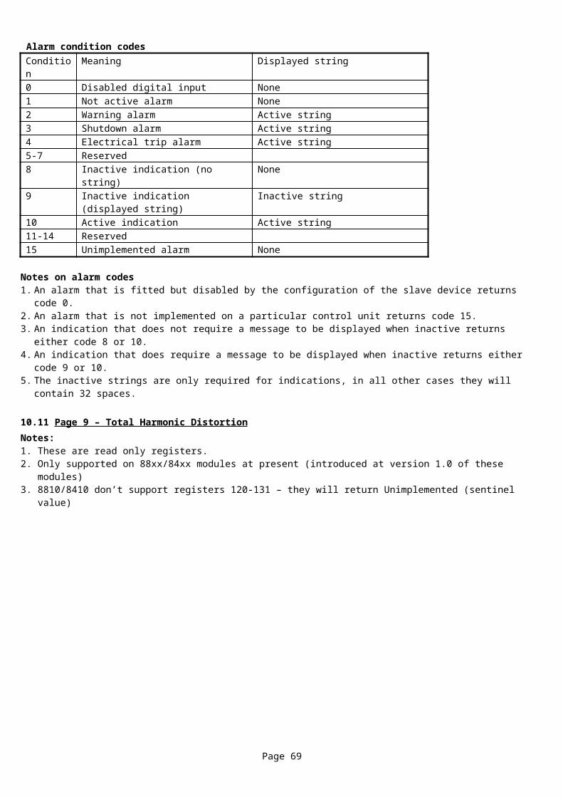
10.30 Pages 59-66 - 2133 Expansion module analogue alarm strings 1. These registers provide the user defined alarm names of each channel of each expansion module when configured as an
analogue input.2. These pages are implemented on the 72xx/73xx, 8xxx/74xx and later families and replace the alarm strings from the old alarm
system.
59 0 2133 Expansion module 0 input A (low) string UNICODE UNICODE 51232 2133 Expansion module 0 input A (high) string UNICODE UNICODE 51264 2133 Expansion module 0 input B (low) string UNICODE UNICODE 51296 2133 Expansion module 0 input B (high) string UNICODE UNICODE 512128 2133 Expansion module 0 input C (low) string UNICODE UNICODE 512160 2133 Expansion module 0 input C (high) string UNICODE UNICODE 512192 2133 Expansion module 0 input D (low) string UNICODE UNICODE 512224 2133 Expansion module 0 input D (high) string UNICODE UNICODE 512
60 0 2133 Expansion module 0 input E (low) string UNICODE UNICODE 51232 2133 Expansion module 0 input E (high) string UNICODE UNICODE 51264 2133 Expansion module 0 input F (low) string UNICODE UNICODE 51296 2133 Expansion module 0 input F (high) string UNICODE UNICODE 512128 2133 Expansion module 0 input G (low) string UNICODE UNICODE 512160 2133 Expansion module 0 input G (high) string UNICODE UNICODE 512192 2133 Expansion module 0 input H (low) string UNICODE UNICODE 512224 2133 Expansion module 0 input H (high) string UNICODE UNICODE 512
61-62 2133 Expansion module 1 input A-H strings UNICODE UNICODE 51263-64 2133 Expansion module 1 input A-H strings UNICODE UNICODE 51265-66 2133 Expansion module 1 input A-H strings UNICODE UNICODE 512
Page 69
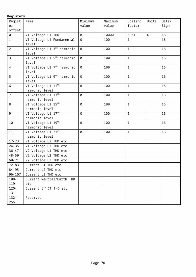
10.31 Page 137 - Active synchronisation and load share configuration
1. These registers may be individually read and written at any time.2. The 72xx/73xx family only supports registers 128-130.
Register offset
Name Minimum value
Maximum value
Scaling factor
Units Bits/ Sign
Read/Write
Local bus control (CAN port 0)0 Device identifier 0 15 1 1 16 Read/Write1-31 Reserved
Miscellaneous 32 Generating set run priority 1 16 1 1 16 Read/Write33 Frequency control offset 0 1.0 0.01 Hz 16 Read/Write34 Reserved 0 0 16 Read/Write35 Reserved 0 0 16 Read/Write36 Load level setting (minimum) 0 100 1 % 16 Read/Write37 Load level setting (maximum) 0 100 1 % 16 Read/Write38 Reserved 0 0 16S Read/Write39 VAr level setting (maximum) -100 100 1 % 16 S Read/Write40 Bus / Mains load setting Bus Mains 16 Read/Write41 Internal governor IF gain 0 10 0.001 V 16 Read/Write42 Internal governor IF offset -10 10 0.001 V 16 S Read/Write43 Internal AVR IF gain 0 10 0.001 V 16 Read/Write44 Internal AVR IF offset -10 10 0.001 V 16 S Read/Write45 Commissioning screens enable flag 0 (no) 1 (yes) 16 Read/Write46-47 Reserved 0 0 16 Read/Write
Frequency synchroniser48 Reserved 0 0 16 Read/Write49 Relay pulse rate 0.5 2.5 0.01 Hz 16 Read/Write50 Relay pulse length 0.1 1.6 0.1 Sec 16 Read/Write51 Gain (proportional gain) 0 0 % 16 Read/Write52 Compensation (integral gain) 0 100 1 % 16 Read/Write52-63 Reserved
Phase synchroniser64-79 Reserved 0 0 16 Read/Write
Page 70
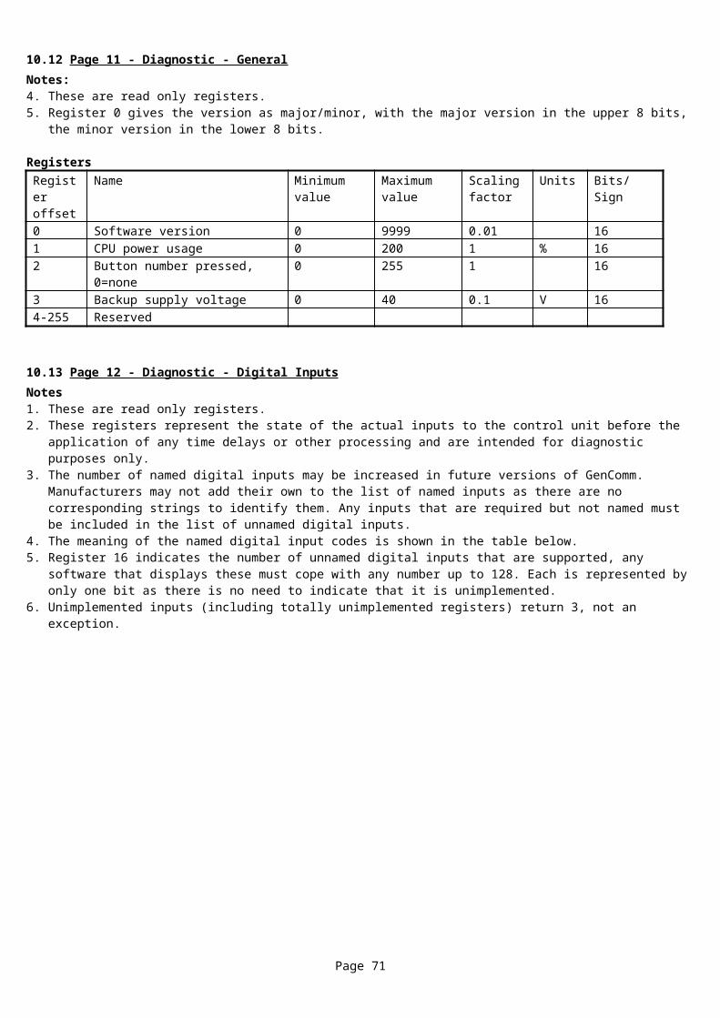
Page 137 registers continuedLoad share
80 Reserved 0 0 16 Read/Write81 Relay pulse rate 0.5 2.5 0.01 Hz 16 Read/Write82 Relay pulse length 0.1 1.6 0.1 Sec 16 Read/Write83 Gain (proportional gain) 0 100 1 % 16 Read/Write84 Compensation (integral gain) 0 100 16 Read/Write85-95 Reserved
Voltage matcher96 Reserved 0 0 16 Read/Write97 Relay pulse rate 0.5 2.5 0.01 Hz 16 Read/Write98 Relay pulse length 0.1 1.6 0.1 Sec 16 Read/Write99 Gain (proportional gain) 0 0 1 % 16 Read/Write100 Compensation (integral gain) 0 100 1 % 16 Read/Write101-111 Reserved
Reactive load control112 Reserved 0 0 16 Read/Write113 Relay pulse rate 0.5 2.5 0.01 Hz 16 Read/Write114 Relay pulse length 0.1 1.6 0.1 Sec 16 Read/Write115 Gain (proportional gain) 0 100 1 % 16 Read/Write116 Compensation (integral gain) 0 0 16 Read/Write117-127 Reserved
Manual frequency trim128 Manual frequency trim -5.0 5.0 0.1 Hz 16S Read/Write129 Minimum frequency trim -5.0 5.0 0.1 Hz 16S Read130 Maximum frequency trim -5.0 5.0 0.1 Hz 16S Read131-136 Reserved136-255 Reserved
Page 71
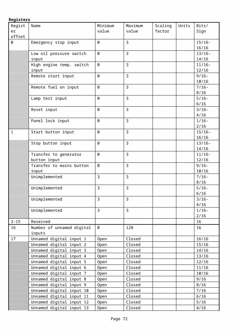
10.32 Page 142 – ECU Trouble Codes
1. Reading register 0 effectively latches a copy of the trouble code list at that time and so allows the list to be read without risk of the contents changing until register 0 is re-read. This also applies to reading the short descriptive strings for the trouble codes (see following pages), so that the list of trouble codes can be read in one or more sections and then the associated strings read as needed. To see any updates to the list, the PC needs to re-read register 0 and so latch the list once more.
RegistersRegister offset
Name Minimum value
Maximum value
Scaling factor
Units Bits/ sign Read/write
0 Number of trouble codes 0 50 16 Read only1 Amber warning lamp status 0 1 1/16 Read only
Red stop lamp status 0 1 2/16 Read onlyReserved for SAE assignment 3-16/16 Read only
2-5 Trouble Code 1 64 Read only6-9 Trouble Code 2 64 Read only10-13 Trouble Code 3 64 Read only14-201 Trouble Codes 4-50 Read only202-255 Reserved Read only
Trouble code formatRegister offset
Name Minimum value
Maximum value
Scaling factor
Units Bits/ Sign
0--1 Trouble code value 0 524287 9-32/32Additional trouble code status 0 255 1-8/32
2 Engine type code 0 31 163 reserved 0 0 16
Page 72
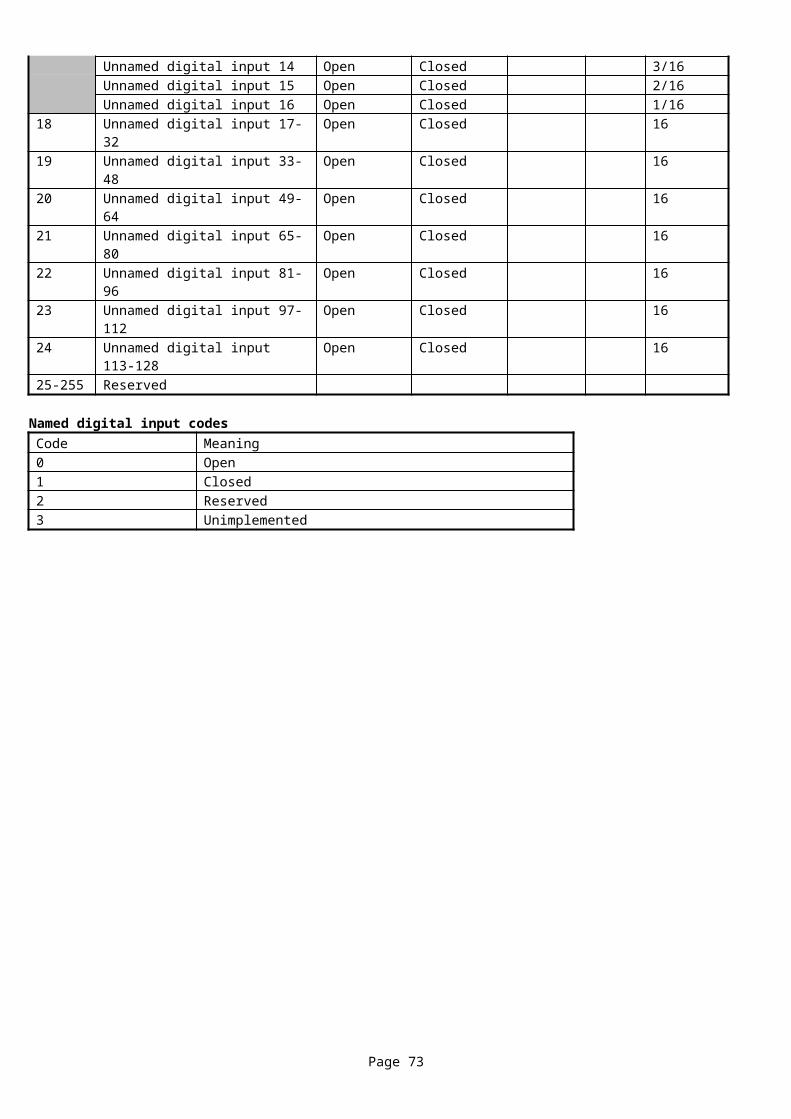
10.33 Page 143-149 – ECU Trouble Code short description string
1. Each short description string is provided with 32x 16 bit registers, one Unicode-16 character in each register. The order of the strings is directly related to the trouble code number position in the list, so trouble code 1 from page 142 will occupy registers 0-31 in page 143, trouble code 2 will occupy registers 32-63 and so on.
2. For now, only page 143 has been implemented to prove the idea, but if it’s acceptable then the extra 6 pages to support a maximum of 50 trouble code strings can be added.
3. A point for discussion is whether we need to add similar look-up facilities for the additional trouble code status strings (FMI for J1939 errors, ACTIVE/PASSIVE indication for Keyword 2000 ECUs etc) for the cases where the PC software isn’t able to locate the required engine module strings on disc as this would require another 7 GenComm pages to provide the look-up for all 50 entries in the list.
4. The reading of the strings is only required when the PC doesn’t have access to its own long version of the strings (such as when the PC doesn’t have the equivalent engine module on disc). The contents of the trouble code list is “frozen” when page 142 register 0 is read so that the PC can read all the trouble code list entries and any strings without the list changing.
Page 73
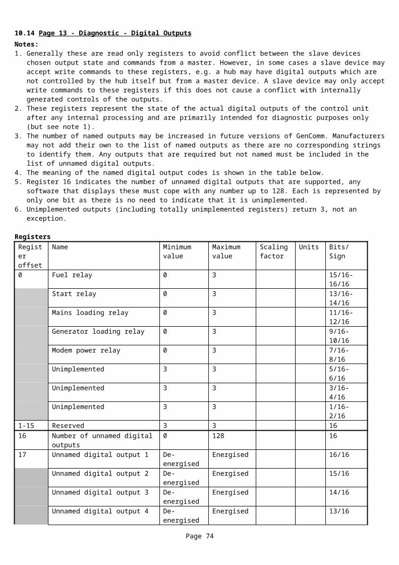
10.34 Page 152 – User calibration of expansion module analogue inputs
1. This provides a similar interface to page 132 but for DSENet expansion modules.2. The 8xxx/74xx family now supports 4x 2130, 10x 2157, 10x 2548, 4x 2131, 4x 2133 and 4x 2152.3. The 335 module supports 2x 2130, 2x 2157, 2x 25484. No provision is made for more than these quantities of each type.
RegistersRegister offset
Name Minimum value
Maximum value
Scaling factor
Units Bits/ sign
Read/write
0-1 2130 Expansion Module 0 input E user scale 0 200 0.1 % 32 Read / write2-3 2130 Expansion Module 0 input F user scale 0 200 0.1 % 32 Read / write4-5 2130 Expansion Module 0 input G user scale 0 200 0.1 % 32 Read / write6-7 2130 Expansion Module 0 input H user scale 0 200 0.1 % 32 Read / write8-15 2130 Expansion Module 1 inputs E-H user scale Read / write16-23 2130 Expansion Module 2 inputs E-H user scale Read / write24-31 2130 Expansion Module 3 inputs E-H user scale Read / write32-33 2131 Expansion Module 0 input A user scale 0 200 0.1 % 32 Read / write34-35 2131 Expansion Module 0 input B user scale 0 200 0.1 % 32 Read / write36-37 2131 Expansion Module 0 input C user scale 0 200 0.1 % 32 Read / write38-39 2131 Expansion Module 0 input D user scale 0 200 0.1 % 32 Read / write40-41 2131 Expansion Module 0 input E user scale 0 200 0.1 % 32 Read / write42-43 2131 Expansion Module 0 input F user scale 0 200 0.1 % 32 Read / write44-45 2131 Expansion Module 0 input G user scale 0 200 0.1 % 32 Read / write46-47 2131 Expansion Module 0 input H user scale 0 200 0.1 % 32 Read / write48-49 2131 Expansion Module 0 input I user scale 0 200 0.1 % 32 Read / write50-51 2131 Expansion Module 0 input J user scale 0 200 0.1 % 32 Read / write52-71 2131 Expansion Module 1 inputs A-J user scale Read / write72-91 2131 Expansion Module 2 inputs A-J user scale Read / write92-111 2131 Expansion Module 3 inputs A-J user scale Read / write112-113 2133 Expansion Module 0 input A user scale 0 200 0.1 % 32 Read / write114-115 2133 Expansion Module 0 input B user scale 0 200 0.1 % 32 Read / write116-117 2133 Expansion Module 0 input C user scale 0 200 0.1 % 32 Read / write118-119 2133 Expansion Module 0 input D user scale 0 200 0.1 % 32 Read / write120-121 2133 Expansion Module 0 input E user scale 0 200 0.1 % 32 Read / write122-123 2133 Expansion Module 0 input F user scale 0 200 0.1 % 32 Read / write124-125 2133 Expansion Module 0 input G user scale 0 200 0.1 % 32 Read / write126-127 2133 Expansion Module 0 input H user scale 0 200 0.1 % 32 Read / write128-143 2133 Expansion Module 1 inputs A-H user scale Read / write144-159 2133 Expansion Module 2 inputs A-H user scale Read / write160-175 2133 Expansion Module 3 inputs A-H user scale Read / write176-255 Reserved
Page 74
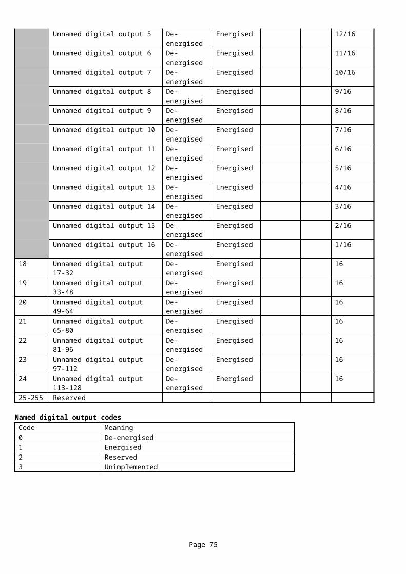
10.35 Page 153 – Unnamed alarm conditions 1. This indicates to the PC the current condition/status of all the unnamed alarm sources, including expansion modules.2. Its operation is very similar to that of page 8 registers 128 & upwards except that the maximum number of supported sources has
been increased to reflect the much larger number of inputs available.3. The 8xxx/74xx family now supports 4x 2130, 10x 2157, 10x 2548, 4x 2131, 4x 2133 and 4x 2152.4. No provision is made for more than these quantities of each type.5. An alarm that is fitted but disabled by the configuration of the slave device returns code 0.6. An alarm that is not implemented on a particular control unit returns code 15.7. An indication that does not require a message to be displayed when inactive returns either code 8 or 10.8. An indication that does require a message to be displayed when inactive returns either code 9 or 10.
72xx/73xx family register allocationRegister offset
Name Minimum value
Maximum value Bits/ Sign
0 Number of unnamed alarm sources 0 256 161 Unnamed digital input 1 0 15 13/16-16/16
Unnamed digital input 2 0 15 9/16-12/16Unnamed digital input 3 0 15 5/16-8/16Unnamed digital input 4 0 15 1/16-4/16
2 Unnamed digital input 5 0 15 13/16-16/16Unnamed digital input 6 0 15 9/16-12/16Unnamed digital input 7 0 15 5/16-8/16Unnamed digital input 8 0 15 1/16-4/16
3 Unnamed digital input 9 0 15 13/16-16/16Reserved for digital input 10 0 15 9/16-12/16Reserved for digital input 11 0 15 5/16-8/16Reserved for digital input 12 0 15 1/16-4/16
4 Reserved for digital inputs 13-165 2130 expansion module 0 digital input A 0 15 13/16-16/16
2130 expansion module 0 digital input B 0 15 9/16-12/162130 expansion module 0 digital input C 0 15 5/16-8/162130 expansion module 0 digital input D 0 15 1/16-4/16
6 2130 expansion module 0 digital input E 0 15 13/16-16/162130 expansion module 0 digital input F 0 15 9/16-12/162130 expansion module 0 digital input G 0 15 5/16-8/162130 expansion module 0 digital input H 0 15 1/16-4/16
7-8 2130 expansion module 1 digital input A-H9-10 2130 expansion module 2 digital input A-H11-12 2130 expansion module 3 digital input A-H13-24 Reserved for expansion modules 4-925 2130 expansion module 0 analogue input E low 0 15 13/16-16/16
2130 expansion module 0 analogue input E high 0 15 9/16-12/162130 expansion module 0 analogue input F low 0 15 5/16-8/162130 expansion module 0 analogue input F high 0 15 1/16-4/16
26 2130 expansion module 0 analogue input G low 0 15 13/16-16/162130 expansion module 0 analogue input G high 0 15 9/16-12/162130 expansion module 0 analogue input H low 0 15 5/16-8/162130 expansion module 0 analogue input H high 0 15 1/16-4/16
27-28 2130 expansion module 1 analogue inputs E-H29-30 2130 expansion module 2 analogue inputs E-H31-32 2130 expansion module 3 analogue inputs E-H33-44 Reserved for 2130 expansion module 4-9 analogue inputs E-H
Page 75
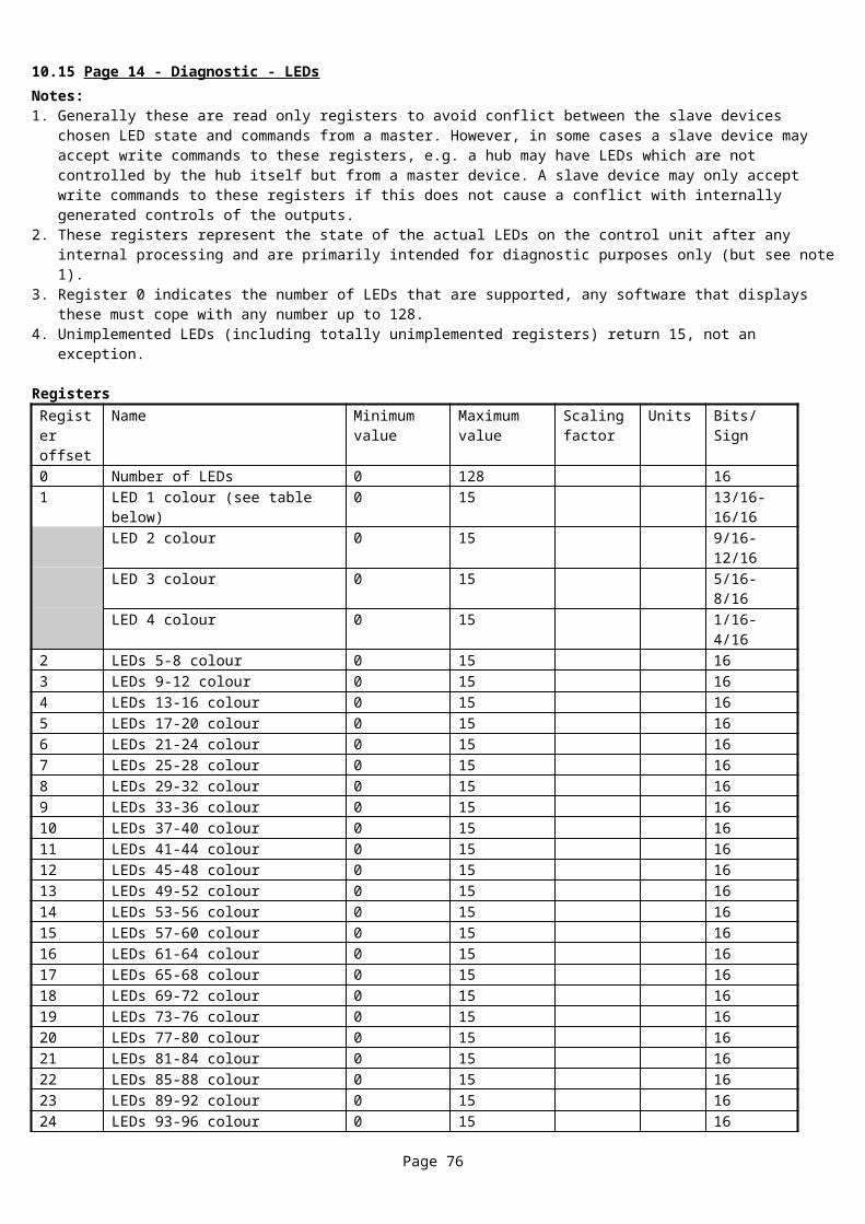
72xx/73xx family register allocation continued45 Internal flexible sender analogue input low 0 15 13/16-16/16
Internal flexible sender analogue input high 0 15 9/16-12/16Maintenance alarm 1 0 15 5/16-8/16Maintenance alarm 2 0 15 1/16-4/16
46 Maintenance alarm 3 0 15 13/16-16/16PLC function 1 0 15 9/16-12/16PLC function 2 0 15 5/16-8/16PLC function 3 0 15 1/16-4/16
47 PLC function 4 0 15 13/16-16/16PLC function 5 0 15 9/16-12/16PLC function 6 0 15 5/16-8/16PLC function 7 0 15 1/16-4/16
48 PLC function 8 0 15 13/16-16/16PLC function 9 0 15 9/16-12/16PLC function 10 0 15 5/16-8/16PLC function 11 0 15 1/16-4/16
49 PLC function 12 0 15 13/16-16/16PLC function 13 0 15 9/16-12/16PLC function 14 0 15 5/16-8/16PLC function 15 0 15 1/16-4/16
50 PLC function 16 0 15 13/16-16/16PLC function 17 0 15 9/16-12/16PLC function 18 0 15 5/16-8/16PLC function 19 0 15 1/16-4/16
51 PLC function 20 0 15 13/16-16/16Unimplemented alarm 0 15 9/16-12/16Unimplemented alarm 0 15 5/16-8/16Unimplemented alarm 0 15 1/16-4/16
47-64 Unimplemented 0 15 1665-255 Reserved
Page 76
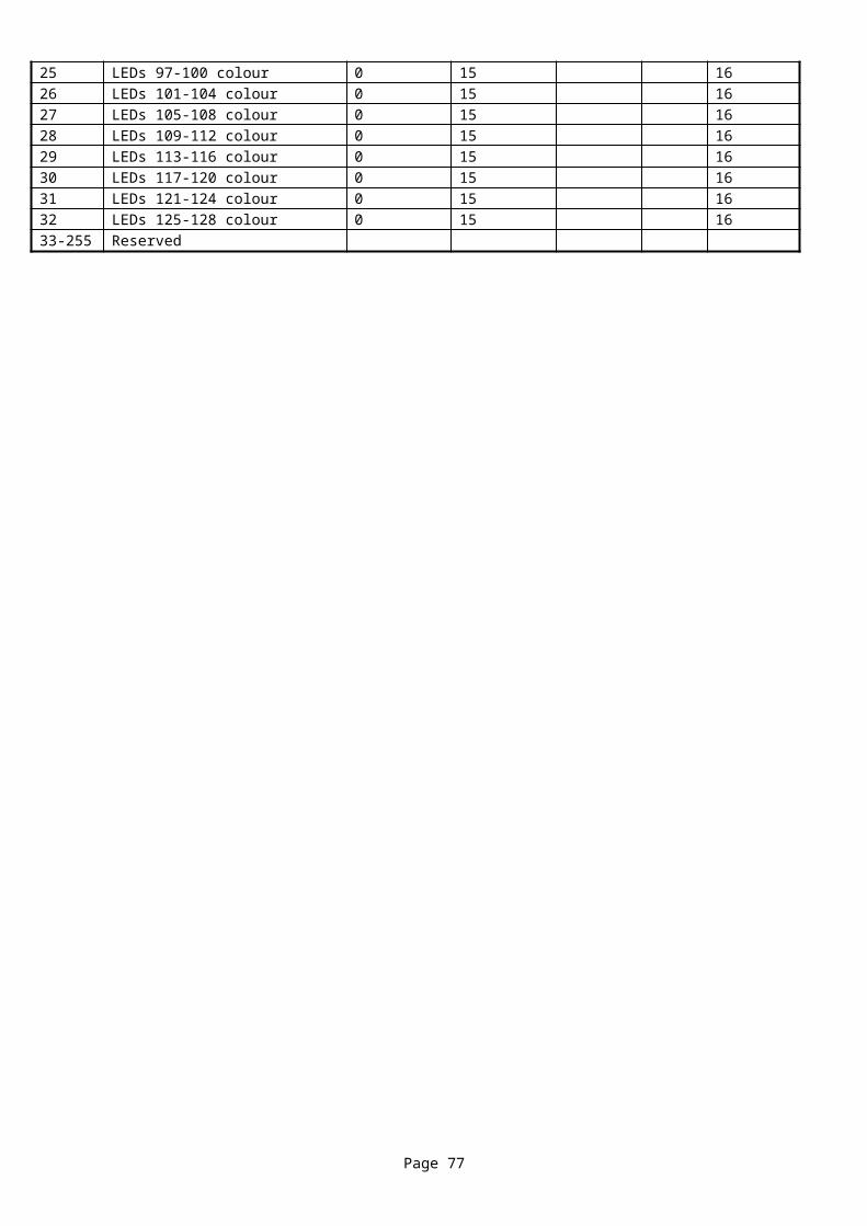
8xxx /74xx family register allocationRegister offset
Name Minimum value Maximum value Bits/ Sign
0 Number of unnamed alarm sources 396 396 161 Unnamed digital input 1 0 15 13/16-16/16
Unnamed digital input 2 0 15 9/16-12/16Unnamed digital input 3 0 15 5/16-8/16Unnamed digital input 4 0 15 1/16-4/16
2 Unnamed digital input 5 0 15 13/16-16/16Unnamed digital input 6 0 15 9/16-12/16Unnamed digital input 7 0 15 5/16-8/16Unnamed digital input 8 0 15 1/16-4/16
3 Unnamed digital input 9 0 15 13/16-16/16Unnamed digital input 10 0 15 9/16-12/16Unnamed digital input 11 0 15 5/16-8/16Unnamed digital input 12 0 15 1/16-4/16
4 Unnamed digital input 13 0 15 13/16-16/16Unnamed digital input 14 0 15 9/16-12/16Unnamed digital input 15 0 15 5/16-8/16Unnamed digital input 16 0 15 1/16-4/16
5 Unnamed digital input 17 0 15 13/16-16/16Unnamed digital input 18 0 15 9/16-12/16Unnamed digital input 19 0 15 5/16-8/16Unnamed digital input 20 0 15 1/16-4/16
6 Unnamed digital input 21 0 15 13/16-16/16Unnamed digital input 22 0 15 9/16-12/16Unnamed digital input 23 0 15 5/16-8/16Unnamed digital input 24 0 15 1/16-4/16
7 Unnamed digital input 25 0 15 13/16-16/16Unnamed digital input 26 0 15 9/16-12/16Unnamed digital input 27 0 15 5/16-8/16Unnamed digital input 28 0 15 1/16-4/16
8 Unnamed digital input 29 0 15 13/16-16/16Unnamed digital input 30 0 15 9/16-12/16Unnamed digital input 31 0 15 5/16-8/16Unnamed digital input 32 0 15 1/16-4/16
9 2130 expansion module 0 digital input A 0 15 13/16-16/162130 expansion module 0 digital input B 0 15 9/16-12/162130 expansion module 0 digital input C 0 15 5/16-8/162130 expansion module 0 digital input D 0 15 1/16-4/16
10 2130 expansion module 0 digital input E 0 15 13/16-16/162130 expansion module 0 digital input F 0 15 9/16-12/162130 expansion module 0 digital input G 0 15 5/16-8/162130 expansion module 0 digital input H 0 15 1/16-4/16
11-12 2130 expansion module 1 digital input A-H13-14 2130 expansion module 2 digital input A-H15-16 2130 expansion module 3 digital input A-H
Page 77
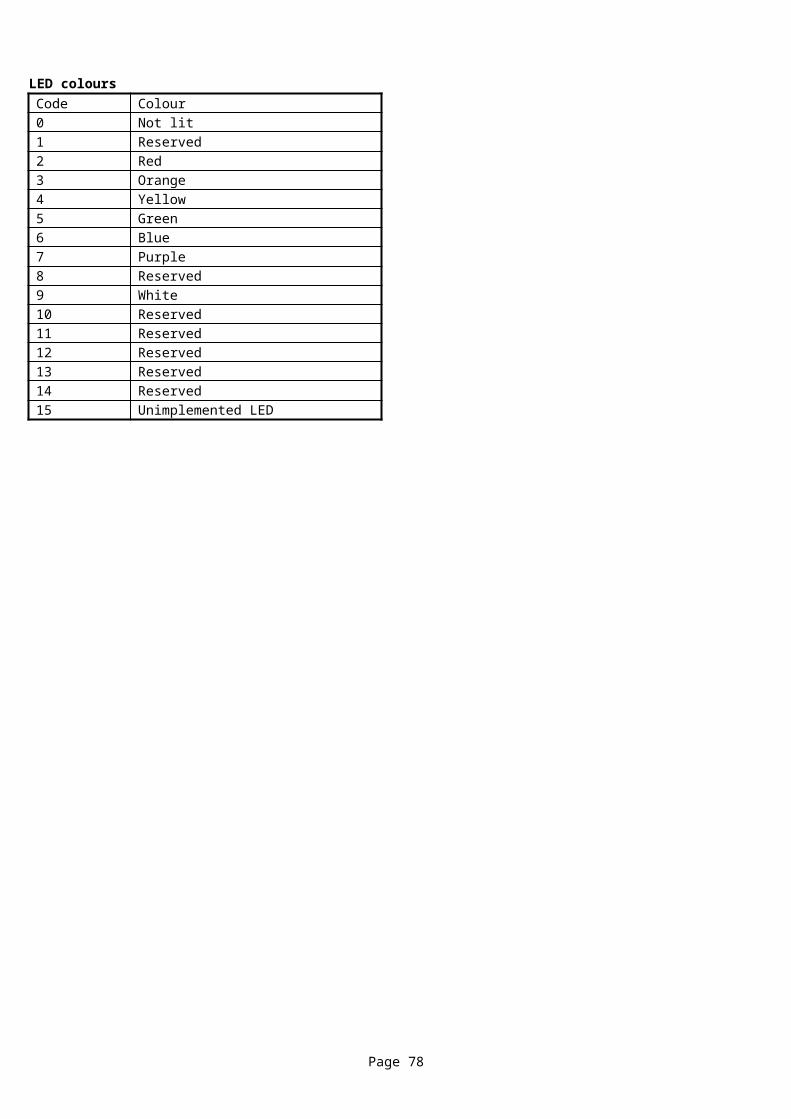
8xxx / 74xx family register allocation continued17 2131 expansion module 0 digital input A 0 15 13/16-16/16
2131 expansion module 0 digital input B 0 15 9/16-12/162131 expansion module 0 digital input C 0 15 5/16-8/162131 expansion module 0 digital input D 0 15 1/16-4/16
18 2131 expansion module 0 digital input E 0 15 13/16-16/162131 expansion module 0 digital input F 0 15 9/16-12/162131 expansion module 0 digital input G 0 15 5/16-8/162131 expansion module 0 digital input H 0 15 1/16-4/16
19 2131 expansion module 0 digital input I 0 15 13/16-16/162131 expansion module 0 digital input J 0 15 9/16-12/162131 expansion module 1 digital input A 0 15 5/16-8/162131 expansion module 1 digital input B 0 15 1/16-4/16
20 2131 expansion module 1 digital input C 0 15 13/16-16/162131 expansion module 1 digital input D 0 15 9/16-12/162131 expansion module 1 digital input E 0 15 5/16-8/162131 expansion module 1 digital input F 0 15 1/16-4/16
21 2131 expansion module 1 digital input G 0 15 13/16-16/162131 expansion module 1 digital input H 0 15 9/16-12/162131 expansion module 1 digital input I 0 15 5/16-8/162131 expansion module 1 digital input J 0 15 1/16-4/16
22 2131 expansion module 2 digital input A 0 15 13/16-16/162131 expansion module 2 digital input B 0 15 9/16-12/162131 expansion module 2 digital input C 0 15 5/16-8/162131 expansion module 2 digital input D 0 15 1/16-4/16
23 2131 expansion module 2 digital input E 0 15 13/16-16/162131 expansion module 2 digital input F 0 15 9/16-12/162131 expansion module 2 digital input G 0 15 5/16-8/162131 expansion module 2 digital input H 0 15 1/16-4/16
24 2131 expansion module 2 digital input I 0 15 13/16-16/162131 expansion module 2 digital input J 0 15 9/16-12/162131 expansion module 3 digital input A 0 15 5/16-8/162131 expansion module 3 digital input B 0 15 1/16-4/16
25 2131 expansion module 3 digital input C 0 15 13/16-16/162131 expansion module 3 digital input D 0 15 9/16-12/162131 expansion module 3 digital input E 0 15 5/16-8/162131 expansion module 3 digital input F 0 15 1/16-4/16
26 2131 expansion module 3 digital input G 0 15 13/16-16/162131 expansion module 3 digital input H 0 15 9/16-12/162131 expansion module 3 digital input I 0 15 5/16-8/162131 expansion module 3 digital input J 0 15 1/16-4/16
27-28 Unimplemented 15 15
Page 78
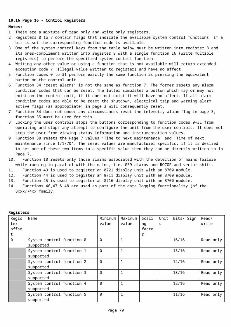
8xxx / 74xx family register allocation continued29 2130 expansion module 0 analogue input E low 0 15 13/16-16/16
2130 expansion module 0 analogue input E high 0 15 9/16-12/162130 expansion module 0 analogue input F low 0 15 5/16-8/162130 expansion module 0 analogue input F high 0 15 1/16-4/16
30 2130 expansion module 0 analogue input G low 0 15 13/16-16/162130 expansion module 0 analogue input G high 0 15 9/16-12/162130 expansion module 0 analogue input H low 0 15 5/16-8/162130 expansion module 0 analogue input H high 0 15 1/16-4/16
31-32 2130 expansion module 1 analogue inputs E-H33-34 2130 expansion module 2 analogue inputs E-H35-36 2130 expansion module 3 analogue inputs E-H37-48 Unimplemented 15 15 1649 Internal flexible sender 1 analogue input low 0 15 13/16-16/16
Internal flexible sender 1 analogue input high 0 15 9/16-12/16Internal flexible sender 2 analogue input low 0 15 5/16-8/16Internal flexible sender 2 analogue input high 0 15 1/16-4/16
50 Internal flexible sender 3 analogue input low 0 15 13/16-16/16Internal flexible sender 3 analogue input high 0 15 9/16-12/16Internal flexible sender 4 analogue input low 0 15 5/16-8/16Internal flexible sender 4 analogue input high 0 15 1/16-4/16
51 Internal flexible sender 5 analogue input low 0 15 13/16-16/16Internal flexible sender 5 analogue input high 0 15 9/16-12/16Maintenance alarm 1 0 15 5/16-8/16Maintenance alarm 2 0 15 1/16-4/16
52 Maintenance alarm 3 0 15 13/16-16/16PLC function 1 0 15 9/16-12/16PLC function 2 0 15 5/16-8/16PLC function 3 0 15 1/16-4/16
53 PLC function 4 0 15 13/16-16/16PLC function 5 0 15 9/16-12/16PLC function 6 0 15 5/16-8/16PLC function 7 0 15 1/16-4/16
54 PLC function 8 0 15 13/16-16/16PLC function 9 0 15 9/16-12/16PLC function 10 0 15 5/16-8/16PLC function 11 0 15 1/16-4/16
55 PLC function 12 0 15 13/16-16/16PLC function 13 0 15 9/16-12/16PLC function 14 0 15 5/16-8/16PLC function 15 0 15 1/16-4/16
56 PLC function 16 0 15 13/16-16/16PLC function 17 0 15 9/16-12/16PLC function 18 0 15 5/16-8/16PLC function 19 0 15 1/16-4/16
57 PLC function 20 0 15 13/16-16/16Unimplemented 0 15 9/16-12/16Unimplemented 0 15 5/16-8/16Unimplemented 0 15 1/16-4/16
58-63 Unimplemented 0 15 16
Page 79
8xxx / 74xx family register allocation continued64 2131 expansion module 0 analogue input A low 0 15 13/16-16/16
2131 expansion module 0 analogue input A high 0 15 9/16-12/162131 expansion module 0 analogue input B low 0 15 5/16-8/162131 expansion module 0 analogue input B high 0 15 1/16-4/16
65 2131 expansion module 0 analogue input C low 0 15 13/16-16/162131 expansion module 0 analogue input C high 0 15 9/16-12/162131 expansion module 0 analogue input D low 0 15 5/16-8/162131 expansion module 0 analogue input D high 0 15 1/16-4/16
66 2131 expansion module 0 analogue input E low 0 15 13/16-16/162131 expansion module 0 analogue input E high 0 15 9/16-12/162131 expansion module 0 analogue input F low 0 15 5/16-8/162131 expansion module 0 analogue input F high 0 15 1/16-4/16
67 2131 expansion module 0 analogue input G low 0 15 13/16-16/162131 expansion module 0 analogue input G high 0 15 9/16-12/162131 expansion module 0 analogue input H low 0 15 5/16-8/162131 expansion module 0 analogue input H high 0 15 1/16-4/16
68 2131 expansion module 0 analogue input I low 0 15 13/16-16/162131 expansion module 0 analogue input I high 0 15 9/16-12/162131 expansion module 0 analogue input J low 0 15 5/16-8/162131 expansion module 0 analogue input J high 0 15 1/16-4/16
69 - 74 2131 expansion module 1 analogue input A – J74 - 78 2131 expansion module 2 analogue input A – J 79 - 83 2131 expansion module 3 analogue input A – J 84 2133 expansion module 0 analogue input A low 0 15 13/16-16/16
2133 expansion module 0 analogue input A high 0 15 9/16-12/162133 expansion module 0 analogue input B low 0 15 5/16-8/162133 expansion module 0 analogue input B high 0 15 1/16-4/16
85 2133 expansion module 0 analogue input C low 0 15 13/16-16/162133 expansion module 0 analogue input C high 0 15 9/16-12/162133 expansion module 0 analogue input D low 0 15 5/16-8/162133 expansion module 0 analogue input D high 0 15 1/16-4/16
86 2133 expansion module 0 analogue input E low 0 15 13/16-16/162133 expansion module 0 analogue input E high 0 15 9/16-12/162133 expansion module 0 analogue input F low 0 15 5/16-8/162133 expansion module 0 analogue input F high 0 15 1/16-4/16
87 2133 expansion module 0 analogue input G low 0 15 13/16-16/162133 expansion module 0 analogue input G high 0 15 9/16-12/162133 expansion module 0 analogue input H low 0 15 5/16-8/162133 expansion module 0 analogue input H high 0 15 1/16-4/16
88 – 91 2133 expansion module 1 analogue input A – H 92 – 95 2133 expansion module 2 analogue input A - H96 – 99 2133 expansion module 3 analogue input A – H 100-255 Reserved
Page 80
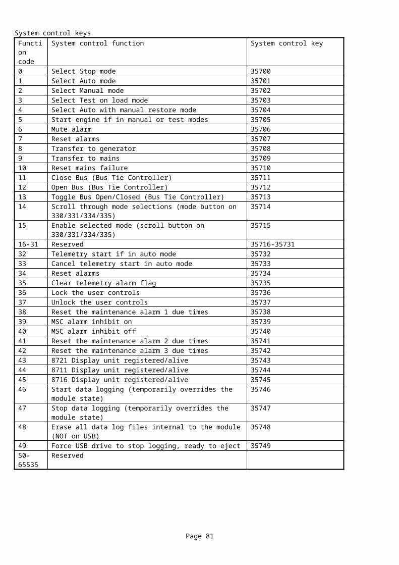
3xx family register allocation1. Unimplemented registers within a family/module are shaded
Register offset
Name Min value
Max value
Bits/ Sign 330
331
332
333
334
335
0 Number of unnamed alarm sources 0 256 16
1 Unnamed digital input A 0 15 13/16-16/16
Unnamed digital input B 0 15 9/16-12/16
Unnamed digital input C 0 15 5/16-8/16
Unnamed digital input D 0 15 1/16-4/16
2 Unnamed digital input E 0 15 13/16-16/16
Unnamed digital input F 0 15 9/16-12/16
Unnamed digital input G 0 15 5/16-8/16
Unnamed digital input H 0 15 1/16-4/16
3 Unnamed digital input I 0 15 13/16-16/16
Unnamed digital input J 0 15 9/16-12/16
Unnamed digital input K 0 15 5/16-8/16
Unnamed digital input L 0 15 1/16-4/16
4 Unimplemented (Reserved for future digital inputs)5 2130 expansion module 0 digital input A 0 15 13/16-16/16
2130 expansion module 0 digital input B 0 15 9/16-12/16
2130 expansion module 0 digital input C 0 15 5/16-8/16
2130 expansion module 0 digital input D 0 15 1/16-4/16
6 2130 expansion module 0 digital input E 0 15 13/16-16/16
2130 expansion module 0 digital input F 0 15 9/16-12/16
2130 expansion module 0 digital input G 0 15 5/16-8/16
2130 expansion module 0 digital input H 0 15 1/16-4/16
7 – 8 2130 expansion module 1 digital inputs A-H
9 – 10 2130 expansion module 2 digital inputs A-H11-12 2130 expansion module 3 digital inputs A-H13-24 Reserved for expansion modules 4-9 digital inputs25 2130 expansion module 0 analogue input E low 0 15 13/16-16/16
2130 expansion module 0 analogue input E high 0 15 9/16-12/16
2130 expansion module 0 analogue input F low 0 15 5/16-8/16
2130 expansion module 0 analogue input F high 0 15 1/16-4/16
26 2130 expansion module 0 analogue input G low 0 15 13/16-16/16
2130 expansion module 0 analogue input G high 0 15 9/16-12/16
2130 expansion module 0 analogue input H low 0 15 5/16-8/16
2130 expansion module 0 analogue input H high 0 15 1/16-4/16
Page 81
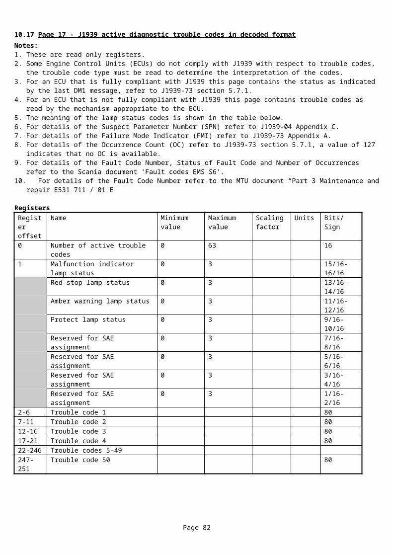
3xx family register allocation continuedRegister offset
Name Min value
Max value
Bits/ Sign 330
331
332
333
334
335
27 - 28 2130 expansion module 1 analogue inputs E-H
29-30 2130 expansion module 2 analogue inputs E-H31-32 2130 expansion module 3 analogue inputs E-H33-44 Unimplemented (Reserved for 2130 expansion
module 4-9 analogue inputs E-H)45 PLC function 1 0 15 13/16-16/16
PLC function 2 0 15 9/16-12/16
PLC function 3 0 15 5/16-8/16
PLC function 4 0 15 1/16-4/16
46 PLC function 5 0 15 13/16-16/16
PLC function 6 0 15 9/16-12/16
PLC function 7 0 15 5/16-8/16
PLC function 8 0 15 1/16-4/16
47 PLC function 9 0 15 13/16-16/16
PLC function 10 0 15 9/16-12/16
PLC function 11 0 15 5/16-8/16
PLC function 12 0 15 1/16-4/16
48 PLC function 13 0 15 13/16-16/16
PLC function 14 0 15 9/16-12/16
PLC function 15 0 15 5/16-8/16
PLC function 16 0 15 1/16-4/16
49 PLC function 17 0 15 13/16-16/16
PLC function 18 0 15 9/16-12/16
PLC function 19 0 15 5/16-8/16
PLC function 20 0 15 1/16-4/16
50-64 Unimplemented 0 15 1665-255 Reserved
Alarm condition codesCondition Meaning Displayed string0 Disabled input None1 Not active alarm None2 Warning alarm Active string3 Shutdown alarm Active string4 Electrical trip alarm Active string5-7 Reserved8 Inactive indication (no string) None9 Inactive indication (displayed string) Inactive string10 Active indication Active string11-14 Reserved15 Unimplemented alarm None
Page 82
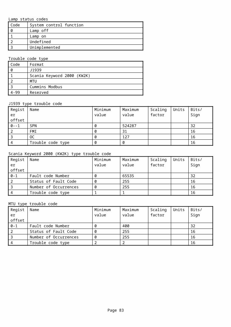
10.36 Page 154 – Named Alarm Conditions
1. This is part of the new alarm system from the 72xx/73xx onwards and replaces page 8.2. Its operation is very similar to that of page 8 registers 0 to 127 except that the supported sources have been re-ordered and are
family specific.3. These are read only registers.4. Each alarm can be in one of 15 conditions as shown in the table below.5. All unimplemented pre-defined alarms return the unimplemented value 15, not an exception.6. Each family has a different list of registers.7. An alarm that is fitted but disabled by the configuration of the slave device returns code 0.8. An alarm that is not implemented on a particular control unit returns code 15.9. An indication that does not require a message to be displayed when inactive returns either code 8 or 10.10. An indication that does require a message to be displayed when inactive returns either code 9 or 10.
72xx/73xx family register allocationRegister offset
Name Minimum value Maximum value Bits/ Sign
0 Number of named alarms 30 256 161 Emergency stop 0 15 13/16-16/16
Low oil pressure 0 15 9/16-12/16High coolant temperature 0 15 5/16-8/16Low coolant temperature 0 15 1/16-4/16
2 Under speed 0 15 13/16-16/16Over speed 0 15 9/16-12/16Generator Under frequency 0 15 5/16-8/16Generator Over frequency 0 15 1/16-4/16
3 Generator low voltage 0 15 13/16-16/16Generator high voltage 0 15 9/16-12/16Battery low voltage 0 15 5/16-8/16Battery high voltage 0 15 1/16-4/16
4 Charge alternator failure 0 15 13/16-16/16Fail to start 0 15 9/16-12/16Fail to stop 0 15 5/16-8/16Generator fail to close 0 15 1/16-4/16
5 Mains fail to close 0 15 13/16-16/16Oil pressure sender fault 0 15 9/16-12/16Loss of magnetic pick up 0 15 5/16-8/16Magnetic pick up open circuit 0 15 1/16-4/16
6 Generator high current 0 15 13/16-16/16Calibration lost 0 15 9/16-12/16Low fuel level 0 15 5/16-8/16CAN ECU Warning 0 15 1/16-4/16
7 CAN ECU Shutdown 0 15 13/16-16/16CAN ECU Data fail 0 15 9/16-12/16Low oil level switch 0 15 5/16-8/16High temperature switch 0 15 1/16-4/16
8 Low fuel level switch 0 15 13/16-16/16Expansion unit watchdog alarm 0 15 9/16-12/16kW overload alarm 0 15 5/16-8/16Negative phase sequence current alarm 0 15 1/16-4/16
9 Earth fault trip alarm 0 15 13/16-16/16Generator phase rotation alarm 0 15 9/16-12/16Auto Voltage Sense Fail 0 15 5/16-8/16Maintenance alarm 0 15 1/16-4/16
Page 83
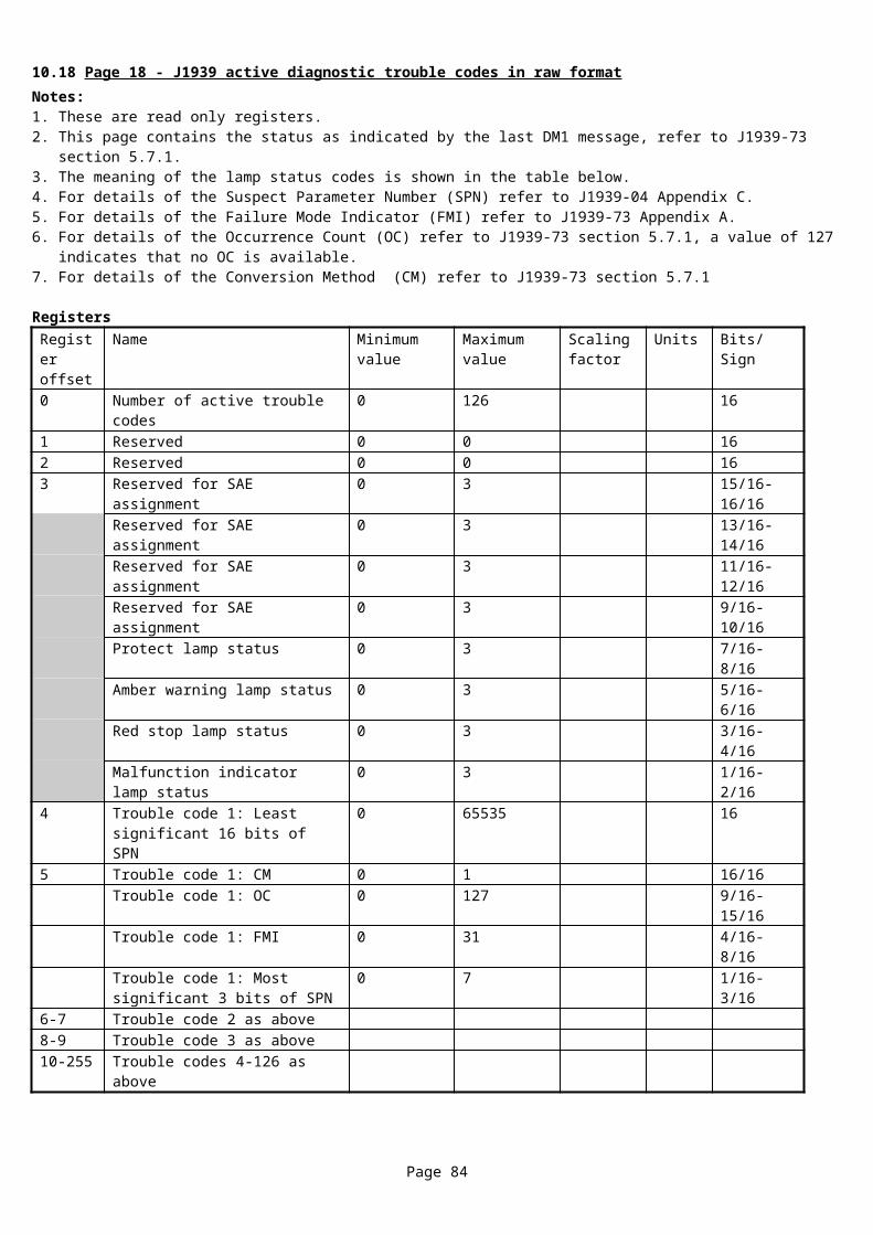
72xx/73xx family register allocation continued10 Loading frequency alarm 0 15 13/16-16/16
Loading voltage alarm 0 15 9/16-12/16Fuel usage running 0 15 5/16-8/16Fuel usage stopped 0 15 1/16-4/16
11 Protections disabled 0 15 13/16-16/16Protections blocked 0 15 9/16-12/16Generator Short Circuit 0 15 5/16-8/16Mains High Current 0 15 1/16-4/16
12 Mains Earth Fault 0 15 13/16-16/16Mains Short Circuit 0 15 9/16-12/16ECU protect 0 15 5/16-8/16ECU Malfunction 0 15 1/16-4/16
13 ECU Information 0 15 13/16-16/16ECU Shutdown 0 15 9/16-12/16ECU Warning 0 15 5/16-8/16ECU Electrical Trip 0 15 1/16-4/16
14 ECU After treatment 0 15 13/16-16/16ECU Water In Fuel 0 15 9/16-12/16Generator Reverse Power 0 15 5/16-8/16Unimplemented 0 15 1/16-4/16
65-255 Reserved
Page 84
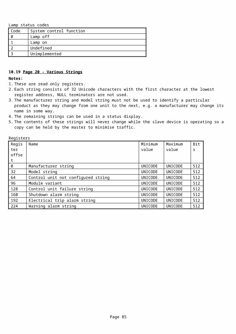
8xxx / 74xx family register allocationRegister offset
Name Minimum value Maximum value Bits/ Sign
0 Number of named alarms 99 256 161 Emergency stop 0 15 13/16-16/16
Low oil pressure 0 15 9/16-12/16High coolant temperature 0 15 5/16-8/16Low coolant temperature 0 15 1/16-4/16
2 Under speed 0 15 13/16-16/16Over speed 0 15 9/16-12/16Generator Under frequency 0 15 5/16-8/16Generator Over frequency 0 15 1/16-4/16
3 Generator low voltage 0 15 13/16-16/16Generator high voltage 0 15 9/16-12/16Battery low voltage 0 15 5/16-8/16Battery high voltage 0 15 1/16-4/16
4 Charge alternator failure 0 15 13/16-16/16Fail to start 0 15 9/16-12/16Fail to stop 0 15 5/16-8/16Generator fail to close 0 15 1/16-4/16
5 Mains fail to close 0 15 13/16-16/16Oil pressure sender fault 0 15 9/16-12/16Loss of magnetic pick up 0 15 5/16-8/16Magnetic pick up open circuit 0 15 1/16-4/16
6 Generator high current 0 15 13/16-16/16Calibration lost 0 15 9/16-12/16Low fuel level 0 15 5/16-8/16CAN ECU Warning 0 15 1/16-4/16
7 CAN ECU Shutdown 0 15 13/16-16/16CAN ECU Data fail 0 15 9/16-12/16Low oil level switch 0 15 5/16-8/16High temperature switch 0 15 1/16-4/16
8 Low fuel level switch 0 15 13/16-16/16Expansion unit watchdog alarm 0 15 9/16-12/16kW overload alarm 0 15 5/16-8/16Negative phase sequence current alarm 0 15 1/16-4/16
9 Earth fault trip alarm 0 15 13/16-16/16Generator phase rotation alarm 0 15 9/16-12/16Auto Voltage Sense Fail 0 15 5/16-8/16Maintenance alarm 0 15 1/16-4/16
10 Loading frequency alarm 0 15 13/16-16/16Loading voltage alarm 0 15 9/16-12/16Fuel usage running 0 15 5/16-8/16Fuel usage stopped 0 15 1/16-4/16
11 Protections disabled 0 15 13/16-16/16Protections blocked 0 15 9/16-12/16Generator breaker failed to open 0 15 5/16-8/16Mains breaker failed to open 0 15 1/16-4/16
12 Bus breaker failed to close 0 15 13/16-16/16Bus breaker failed to open 0 15 9/16-12/16Generator reverse power alarm 0 15 5/16-8/16Short circuit alarm 0 15 1/16-4/16
13 Air flap closed alarm 0 15 13/16-16/16Failure to sync 0 15 9/16-12/16Bus live 0 15 5/16-8/16Bus not live 0 15 1/16-4/16
Page 85
8xxx / 74xx family register allocations continued14 Bus phase rotation 0 15 13/16-16/16
Priority selection error 0 15 9/16-12/16MSC data error 0 15 5/16-8/16MSC ID error 0 15 1/16-4/16
15 Bus low voltage 0 15 13/16-16/16Bus high voltage 0 15 9/16-12/16Bus low frequency 0 15 5/16-8/16Bus high frequency 0 15 1/16-4/16
16 MSC failure 0 15 13/16-16/16MSC too few sets 0 15 9/16-12/16MSC alarms inhibited 0 15 5/16-8/16MSC old version units on the bus 0 15 1/16-4/16
17 Mains reverse power alarm/mains export alarm 0 15 13/16-16/16Minimum sets not reached 0 15 9/16-12/16Insufficient capacity 0 15 5/16-8/16Out of sync 0 15 1/16-4/16
18 Alternative aux mains fail 0 15 13/16-16/16Loss of excitation 0 15 9/16-12/16Mains ROCOF 0 15 5/16-8/16Mains vector shift 0 15 1/16-4/16
19 Mains decoupling low frequency 0 15 13/16-16/16Mains decoupling high frequency 0 15 9/16-12/16Mains decoupling low voltage 0 15 5/16-8/16Mains decoupling high voltage 0 15 1/16-4/16
20 Mains decoupling combined alarm 0 15 13/16-16/16Charge air temperature 0 15 9/16-12/16Mains phase rotation alarm identifier 0 15 5/16-8/16AVR Max Trim Limit alarm 0 15 1/16-4/16
21 High coolant temperature electrical trip alarm 0 15 13/16-16/16Temperature sender open circuit alarm 0 15 9/16-12/16Out of sync Bus 0 15 5/16-8/16Out of sync Mains 0 15 1/16-4/16
22 Bus 1 live 0 15 13/16-16/16Bus 1 phase rotation 0 15 9/16-12/16Bus 2 live 0 15 5/16-8/16Bus 2 phase rotation 0 15 1/16-4/16
23 Out of sync Mains (Aux Mains Fail) 0 15 13/16-16/16ECU Protect 0 15 9/16-12/16ECU Malfunction 0 15 5/16-8/16ECU Information 0 15 1/16-4/16
24 ECU Shutdown 0 15 13/16-16/16ECU Warning 0 15 9/16-12/16ECU Electrical Trip 0 15 5/16-8/16ECU After-treatment 0 15 1/16-4/16
25 Water In Fuel 0 15 13/16-16/16ECU Heater 0 15 9/16-12/16ECU Cooler 0 15 5/16-8/16Unimplemented 0 15 1/16-4/16
26-64 Unimplemented65-255 Reserved
Page 86
332/333 register allocationRegister offset
Name Minimum value Maximum value Bits/ Sign
0 Number of named alarms 0 256 161 Battery High Voltage 0 15 13/16-16/16
Battery Low Voltage 0 15 9/16-12/16Generator Failure Latched 0 15 5/16-8/16Generator Failure Unlatched 0 15 1/16-4/16
2 Mains Failure Latched 0 15 13/16-16/16Mains Failure Unlatched 0 15 9/16-12/16Fail to start 0 15 5/16-8/16Fail to stop 0 15 1/16-4/16
3 Failed to reach loading voltage 0 15 13/16-16/16Failed to reach loading frequency 0 15 9/16-12/16Unimplemented 0 15 5/16-8/16Unimplemented 0 15 1/16-4/16
4-64 Unimplemented65-255 Reserved
330/331/334/335 register allocationRegister offset
Name Minimum value Maximum value Bits/ Sign
0 Number of named alarms 0 256 161 Battery High Voltage 0 15 13/16-16/16
Battery Low Voltage 0 15 9/16-12/16S2 Failure Latched 0 15 5/16-8/16S2 Failure Unlatched 0 15 1/16-4/16
2 S1 Failure Latched 0 15 13/16-16/16S1 Failure Unlatched 0 15 9/16-12/16Fail to start 0 15 5/16-8/16Fail to stop 0 15 1/16-4/16
3 Failed to reach loading voltage 0 15 13/16-16/16Failed to reach loading frequency 0 15 9/16-12/16Expansion unit watchdog alarm (335 only) 0 15 5/16-8/16Unimplemented 0 15 1/16-4/16
4-64 Unimplemented65-255 Reserved
Alarm condition codesCondition Meaning Displayed string0 Disabled input None1 Not active alarm None2 Warning alarm Active string3 Shutdown alarm Active string4 Electrical trip alarm Active string5-7 Reserved8 Inactive indication (no string) None9 Inactive indication (displayed string) Inactive string10 Active indication Active string11-14 Reserved15 Unimplemented alarm None
Page 87
10.37 Page 156 – Expansion module enable status 1. This page indicates which expansion modules are currently included in the configuration.2. The 72xx does not support expansion modules so all registers return false.3. The 73xx currently only supports the 2130, 2157 and 2548.4. The 335 currently only supports the 2130, 2157 and 2548.5. False = 0, True =1.6. These registers are Read-Only7. Unimplemented registers within a family/module are shaded
Page 88
RegistersRegister offset
Name Minimum value
Maximum value
Scaling factor
Units Bits/ sign 8xxx/ 74xx
73xx
335
0 2130 Expansion module 0 enable False True 16
1 2130 Expansion module 1 enable False True 16
2 2130 Expansion module 2 enable False True 16
3 2130 Expansion module 3 enable False True 16
4 2130 Expansion module 4 enable False True 16
5 2130 Expansion module 5 enable False True 166 2130 Expansion module 6 enable False True 167 2130 Expansion module 7 enable False True 168 2130 Expansion module 8 enable False True 169 2130 Expansion module 9 enable False True 1610 2157 Expansion module 0 enable False True 16
11 2157 Expansion module 1 enable False True 16
12 2157 Expansion module 2 enable False True 16
13 2157 Expansion module 3 enable False True 16
14 2157 Expansion module 4 enable False True 16
15 2157 Expansion module 5 enable False True 16
16 2157 Expansion module 6 enable False True 16
17 2157 Expansion module 7 enable False True 16
18 2157 Expansion module 8 enable False True 16
19 2157 Expansion module 9 enable False True 16
20 2548 Expansion module 0 enable False True 16
21 2548 Expansion module 1 enable False True 16
22 2548 Expansion module 2 enable False True 16
23 2548 Expansion module 3 enable False True 16
24 2548 Expansion module 4 enable False True 16
25 2548 Expansion module 5 enable False True 16
26 2548 Expansion module 6 enable False True 16
27 2548 Expansion module 7 enable False True 16
28 2548 Expansion module 8 enable False True 16
29 2548 Expansion module 9 enable False True 16
30 2131 Expansion module 0 enable False True 16
31 2131 Expansion module 1 enable False True 16
32 2131 Expansion module 2 enable False True 16
33 2131 Expansion module 3 enable False True 16
34 2133 Expansion module 0 enable False True 16
35 2133 Expansion module 1 enable False True 16
36 2133 Expansion module 2 enable False True 16
37 2133 Expansion module 3 enable False True 16
38 2152 Expansion module 0 enable False True 16
39 2152 Expansion module 1 enable False True 16
40 2152 Expansion module 2 enable False True 16
41 2152 Expansion module 3 enable False True 16
42 2510/20 Expansion module 0 enable NO YES 16
43 2510/20 Expansion module 1 enable NO YES 16
44 2510/20 Expansion module 2 enable NO YES 16
45-255 Reserved
Page 89
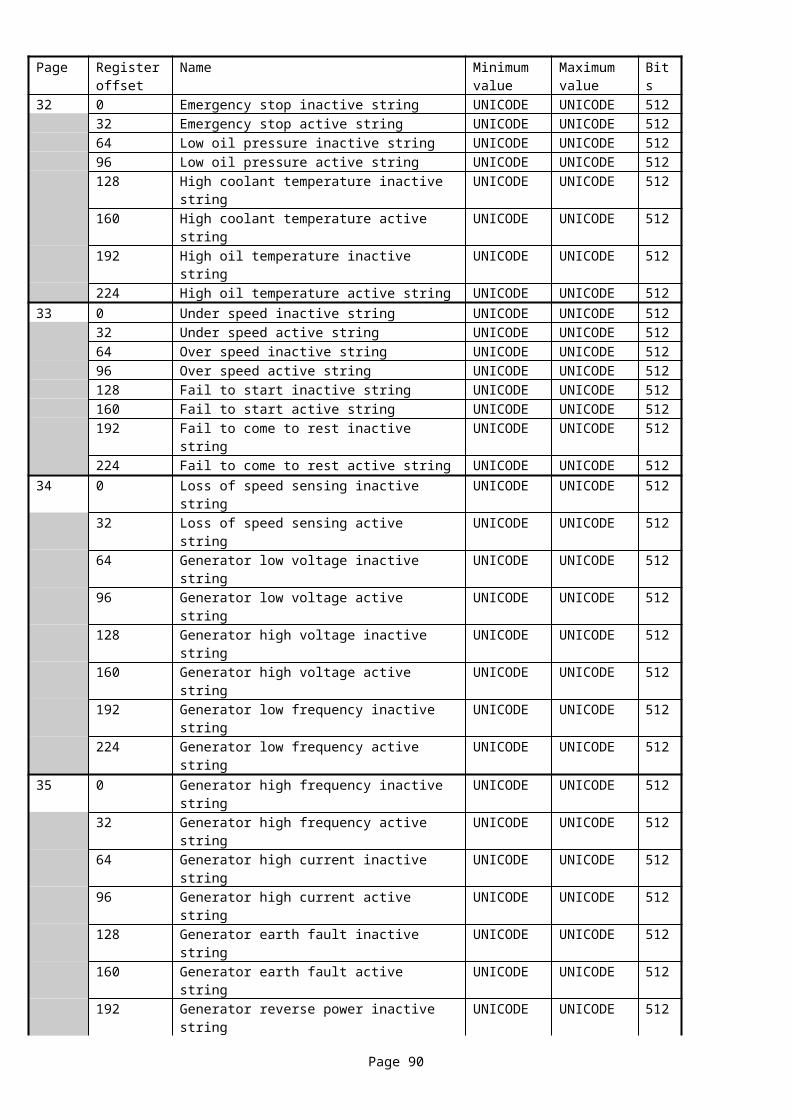
10.38 Page 158 – Expansion module communications status 2. This indicates which expansion modules are failing to communicate with the host module.3. If an expansion module is not enabled in the configuration, it will not report a failure to communicate.4. False = 0, True =1.5. These registers are Read-Only6. Unimplemented registers within a family/module are shaded
Page 90
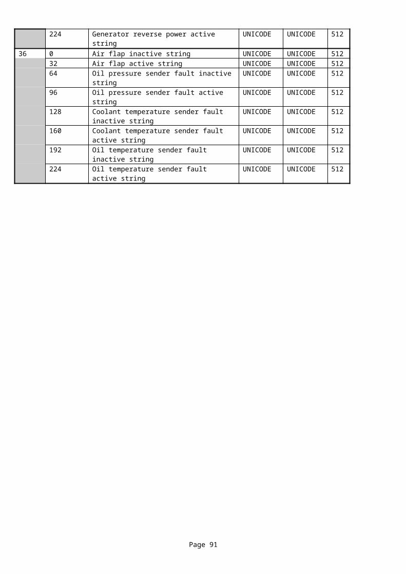
RegistersRegister offset
Name Minimum value
Maximum value
Scaling factor
Units Bits/ sign 8xxx/ 74xx
73xx
335
0 2130 Expansion module 0 comms failure False True 16
1 2130 Expansion module 1 comms failure False True 16
2 2130 Expansion module 2 comms failure False True 16
3 2130 Expansion module 3 comms failure False True 16
4 2130 Expansion module 4 comms failure False True 16
5 2130 Expansion module 5 comms failure False True 166 2130 Expansion module 6 comms failure False True 167 2130 Expansion module 7 comms failure False True 168 2130 Expansion module 8 comms failure False True 169 2130 Expansion module 9 comms failure False True 1610 2157 Expansion module 0 comms failure False True 16
11 2157 Expansion module 1 comms failure False True 16
12 2157 Expansion module 2 comms failure False True 16
13 2157 Expansion module 3 comms failure False True 16
14 2157 Expansion module 4 comms failure False True 16
15 2157 Expansion module 5 comms failure False True 16
16 2157 Expansion module 6 comms failure False True 16
17 2157 Expansion module 7 comms failure False True 16
18 2157 Expansion module 8 comms failure False True 16
19 2157 Expansion module 9 comms failure False True 16
20 2548 Expansion module 0 comms failure False True 16
21 2548 Expansion module 1 comms failure False True 16
22 2548 Expansion module 2 comms failure False True 16
23 2548 Expansion module 3 comms failure False True 16
24 2548 Expansion module 4 comms failure False True 16
25 2548 Expansion module 5 comms failure False True 16
26 2548 Expansion module 6 comms failure False True 16
27 2548 Expansion module 7 comms failure False True 16
28 2548 Expansion module 8 comms failure False True 16
29 2548 Expansion module 9 comms failure False True 16
30 2131 Expansion module 0 comms failure False True 16
31 2131 Expansion module 1 comms failure False True 16
32 2131 Expansion module 2 comms failure False True 16
33 2131 Expansion module 3 comms failure False True 16
34 2133 Expansion module 0 comms failure False True 16
35 2134 Expansion module 1 comms failure False True 16
36 2135 Expansion module 2 comms failure False True 16
37 2136 Expansion module 3 comms failure False True 16
38 2152 Expansion module 0 comms failure False True 16
39 2152 Expansion module 1 comms failure False True 16
40 2152 Expansion module 2 comms failure False True 16
41 2152 Expansion module 3 comms failure False True 16
42-255 Reserved
Page 91

10.39 Page 160 – Unnamed input function
1. This indicates to the PC software how each digital input, both built in and in the expansion modules, is configured.2. A digital input function is the function field from the alarm block.3. Each family has different register allocations.4. Registers 112-159 return unimplemented on the 8xxx/74xx.5. Registers 192-197 on the 8xxx/74xx actually return the function from the digital alarm blocks for the flexible senders; they
duplicate the values returned in registers 16-18. 6. Registers 205-224 were not in this document but are in the 8xxx/74xx code, they need checking.7. These registers are Read-Only.
Page 92
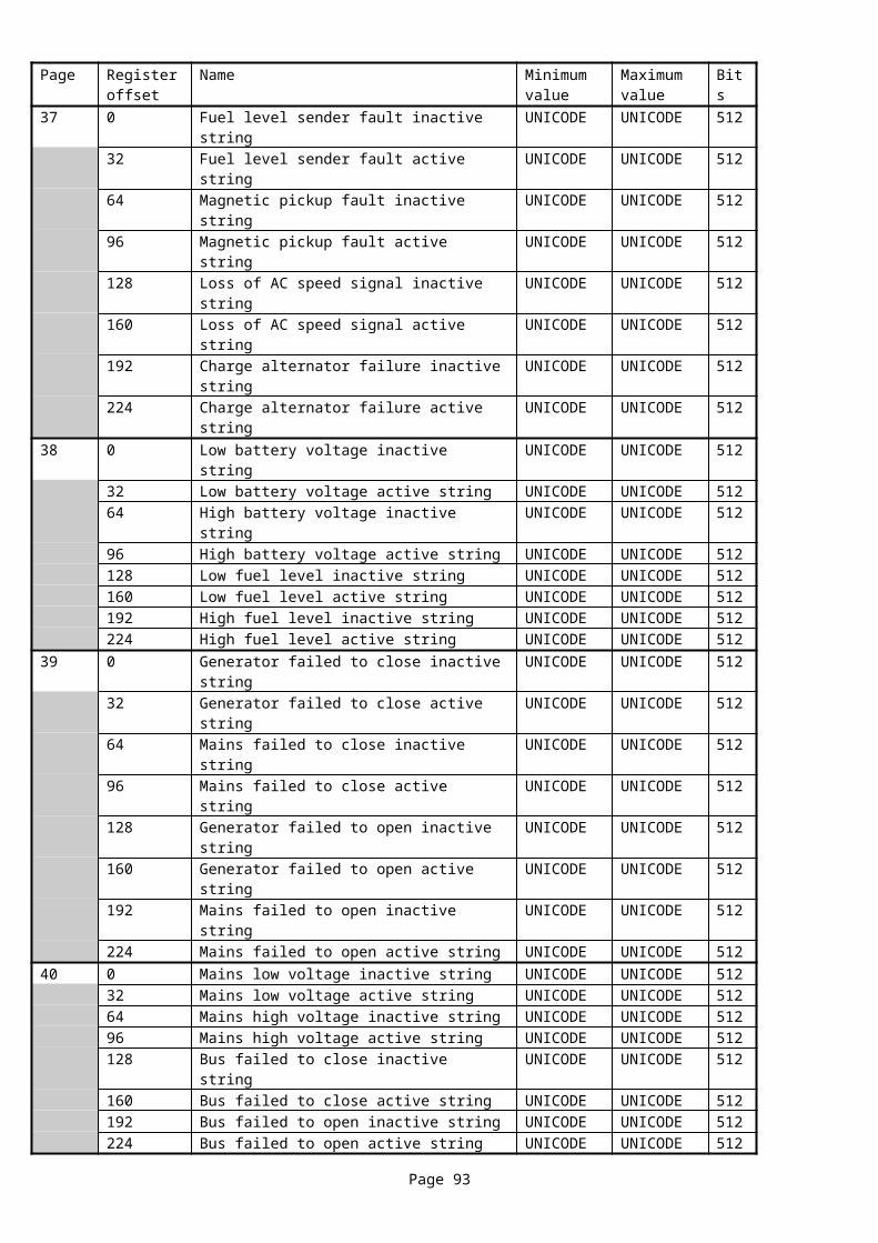
72xx/73xx family register allocationRegister offset
Name Minimum value
Maximum value
Bits/ sign
0 Digital input A function 0 65535 161 Digital input B function 0 65535 162 Digital input C function 0 65535 163 Digital input D function 0 65535 164 Digital input E function 0 65535 165 Digital input F function 0 65535 166 Digital input G function 0 65535 167 Digital input H function 0 65535 168 Digital input I function 0 65535 169-15 Reserved16 2130 Expansion module 0 digital input A 0 65535 1617 2130 Expansion module 0 digital input B 0 65535 1618 2130 Expansion module 0 digital input C 0 65535 1619 2130 Expansion module 0 digital input D 0 65535 1620 2130 Expansion module 0 digital input E 0 65535 1621 2130 Expansion module 0 digital input F 0 65535 1622 2130 Expansion module 0 digital input G 0 65535 1623 2130 Expansion module 0 digital input H 0 65535 1624-31 2130 Expansion module 1 digital inputs A-H32-39 2130 Expansion module 2 digital inputs A-H40-47 2130 Expansion module 3 digital inputs A-H48-95 Reserved for 2130 expansion module 4-9 inputs A-H96 2130 Expansion module 0 analogue input E (low) 0 65535 1697 2130 Expansion module 0 analogue input E (high) 0 65535 1698 2130 Expansion module 0 analogue input F (low) 0 65535 1699 2130 Expansion module 0 analogue input F (high) 0 65535 16100 2130 Expansion module 0 analogue input G (low) 0 65535 16101 2130 Expansion module 0 analogue input G (high) 0 65535 16102 2130 Expansion module 0 analogue input H (low) 0 65535 16103 2130 Expansion module 0 analogue input H (high) 0 65535 16104-111 2130 Expansion module 1 analogue inputs E-H112-119 2130 Expansion module 2 analogue inputs E-H120-127 2130 Expansion module 3 analogue inputs E-H128-175 2130 Expansion module 4-9 analogue inputs E-H176 Internal flexible sender input (low) 0 65535 16177 Internal flexible sender input (high) 0 65535 16178 Maintenance alarm 1 0 65535 16179 Maintenance alarm 2 0 65535 16180 Maintenance alarm 3 0 65535 16181 PLC function 1 0 65535 16182 PLC function 2 0 65535 16183 PLC function 3 0 65535 16184 PLC function 4 0 65535 16185 PLC function 5 0 65535 16186 PLC function 6 0 65535 16187 PLC function 7 0 65535 16188 PLC function 8 0 65535 16189 PLC function 9 0 65535 16190 PLC function 10 0 65535 16191 PLC function 11 0 65535 16192 PLC function 12 0 65535 16193 PLC function 13 0 65535 16194 PLC function 14 0 65535 16195 PLC function 15 0 65535 16196 PLC function 16 0 65535 16197 PLC function 17 0 65535 16
Page 93
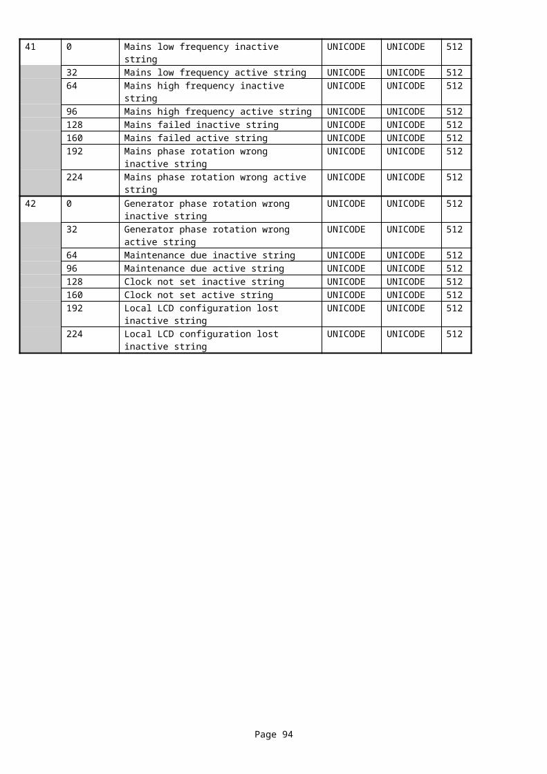
72xx/73xx family register allocation continued198 PLC function 18 0 65535 16199 PLC function 19 0 65535 16200 PLC function 20 0 65535 16201-255 Reserved
8xxx / 74xx family register allocationRegister offset
Name Min value Max value Bits/ sign
0 Digital input A function 0 65535 161 Digital input B function 0 65535 162 Digital input C function 0 65535 163 Digital input D function 0 65535 164 Digital input E function 0 65535 165 Digital input F function 0 65535 166 Digital input G function 0 65535 167 Digital input H function 0 65535 168 Digital input I function 0 65535 169 Digital input J function 0 65535 1610 Digital input K function 0 65535 1611 Digital input L function 0 65535 1612 Digital input M function 0 65535 1613 Digital input N function 0 65535 1614 Digital input O function 0 65535 1615 Digital input P function 0 65535 1616 Digital input Q function 0 65535 1617 Digital input R function 0 65535 1618 Digital input S function 0 65535 1619 Digital input T function 0 65535 1620 Digital input U function 0 65535 1621 Digital input V function 0 65535 1622 Digital input W function 0 65535 1623 Digital input X function 0 65535 1624 Digital input Y function 0 65535 1625 Digital input Z function 0 65535 1626 Digital input AA function 0 65535 1627 Digital input AB function 0 65535 1628 Digital input AC function 0 65535 1629 Digital input AD function 0 65535 1630 Digital input AE function 0 65535 1631 Digital input AF function 0 65535 1632 2130 Expansion module 0 digital input A function 0 65535 1633 2130 Expansion module 0 digital input B function 0 65535 1634 2130 Expansion module 0 digital input C function 0 65535 1635 2130 Expansion module 0 digital input D function 0 65535 1636 2130 Expansion module 0 digital input E function 0 65535 1637 2130 Expansion module 0 digital input F function 0 65535 1638 2130 Expansion module 0 digital input G function 0 65535 1639 2130 Expansion module 0 digital input H function 0 65535 1640-47 2130 Expansion module 1 digital inputs A-H functions48-55 2130 Expansion module 2 digital inputs A-H functions56-63 2130 Expansion module 3 digital inputs A-H functions
Page 94

8xxx / 74xx family register allocation continued64 2131 Expansion module 0 digital input A function 0 65535 1665 2131 Expansion module 0 digital input B function 0 65535 1666 2131 Expansion module 0 digital input C function 0 65535 1667 2131 Expansion module 0 digital input D function 0 65535 1668 2131 Expansion module 0 digital input E function 0 65535 1669 2131 Expansion module 0 digital input F function 0 65535 1670 2131 Expansion module 0 digital input G function 0 65535 1671 2131 Expansion module 0 digital input H function 0 65535 1672 2131 Expansion module 0 digital input I function 0 65535 1673 2131 Expansion module 0 digital input J function 0 65535 1674-83 2131 Expansion module 1 digital inputs A-J functions84-93 2131 Expansion module 2 digital inputs A-J functions94-103 2131 Expansion module 3 digital inputs A-J functions104-111 Reserved112 2130 Expansion module 0 analogue input E (low) 0 65535 16113 2130 Expansion module 0 analogue input E (high) 0 65535 16114 2130 Expansion module 0 analogue input F (low) 0 65535 16115 2130 Expansion module 0 analogue input F (high) 0 65535 16116 2130 Expansion module 0 analogue input G (low) 0 65535 16117 2130 Expansion module 0 analogue input G (high) 0 65535 16118 2130 Expansion module 0 analogue input H (low) 0 65535 16119 2130 Expansion module 0 analogue input H (high) 0 65535 16120-127 2130 Expansion module 1 analogue inputs E-H128-135 2130 Expansion module 2 analogue inputs E-H136-143 2130 Expansion module 3 analogue inputs E-H144-159 Reserved for 2130 Expansion module 4-9 analogue
inputs E-H192 Internal flexible sender 1 input (low) 0 65535 16193 Internal flexible sender 1 input (high) 0 65535 16194 Internal flexible sender 2 input (low) 0 65535 16195 Internal flexible sender 2 input (high) 0 65535 16196 Internal flexible sender 3 input (low) 0 65535 16197 Internal flexible sender 3 input (high) 0 65535 16198 Internal flexible sender 4 input (low) 0 65535 16199 Internal flexible sender 4 input (high) 0 65535 16200 Internal flexible sender 5 input (low) 0 65535 16201 Internal flexible sender 5 input (high) 0 65535 16202 Maintenance alarm 1 function 0 65535 16203 Maintenance alarm 2 function 0 65535 16204 Maintenance alarm 3 function 0 65535 16205 PLC function 1 0 65535 16206 PLC function 2 0 65535 16207 PLC function 3 0 65535 16208 PLC function 4 0 65535 16209 PLC function 5 0 65535 16210 PLC function 6 0 65535 16211 PLC function 7 0 65535 16212 PLC function 8 0 65535 16213 PLC function 9 0 65535 16214 PLC function 10 0 65535 16215 PLC function 11 0 65535 16216 PLC function 12 0 65535 16217 PLC function 13 0 65535 16218 PLC function 14 0 65535 16219 PLC function 15 0 65535 16220 PLC function 16 0 65535 16221 PLC function 17 0 65535 16222 PLC function 18 0 65535 16223 PLC function 19 0 65535 16
Page 95
8xxx/74xx family register allocation continued224 PLC function 20 0 65535 16225-255 Reserved
3xx family register allocation
1. The 335 module supports expansion units (2130, 2157 and 2548) and PLC facilities.2. Unimplemented registers within a family/module are shaded
Register offset
Name Min value
Max value
Bits/ sign
330
331
332
333
334
335
0 Digital input A function 0 65535 16
1 Digital input B function 0 65535 16
2 Digital input C function 0 65535 16
3 Digital input D function 0 65535 16
4 Digital input E function 0 65535 16
5 Digital input F function 0 65535 16
6 Digital input G function 0 65535 16
7 Digital input H function 0 65535 16
8 Digital input I function 0 65535 16
9 Digital input J function 0 65535 16
10 Digital input K function 0 65535 16
11 Digital input L function 0 65535 16
12-15 Unimplemented (reserved for future digital inputs)16 2130 Expansion module 0 digital input A function 0 65535 16
17 2130 Expansion module 0 digital input B function 0 65535 16
18 2130 Expansion module 0 digital input C function 0 65535 16
19 2130 Expansion module 0 digital input D function 0 65535 16
20 2130 Expansion module 0 digital input E function 0 65535 16
21 2130 Expansion module 0 digital input F function 0 65535 16
22 2130 Expansion module 0 digital input G function 0 65535 16
23 2130 Expansion module 0 digital input H function 0 65535 16
24-31 2130 Expansion module 1 digital inputs A-H functions 0 65535 16
32-39 Reserved for 2130 Expansion module 2 digital inputs40-47 Reserved for 2130 Expansion module 3 digital inputs48-95 Reserved for 2130 expansion module 4-9 inputs A-H96 2130 Expansion module 0 analogue input E (low) 0 65535 16
97 2130 Expansion module 0 analogue input E (high) 0 65535 16
98 2130 Expansion module 0 analogue input F (low) 0 65535 16
99 2130 Expansion module 0 analogue input F (high) 0 65535 16
100 2130 Expansion module 0 analogue input G (low) 0 65535 16
101 2130 Expansion module 0 analogue input G (high) 0 65535 16
102 2130 Expansion module 0 analogue input H (low) 0 65535 16
103 2130 Expansion module 0 analogue input H (high) 0 65535 16
104-111 2130 Expansion module 1 analogue inputs E-H 0 65535 16
112-119 Reserved for 2130 Expansion module 2 analogue inputs120-127 Reserved for 2130 Expansion module 3 analogue inputs128-175 Reserved for 2130 Expansion module 4-9 analogue
inputs
Page 96
3xx family register allocation continuedRegister offset
Name Min value
Max value
Bits/ sign
330
331
332
333
334
335
176 PLC function 1 0 65535 16
177 PLC function 2 0 65535 16
178 PLC function 3 0 65535 16
179 PLC function 4 0 65535 16
180 PLC function 5 0 65535 16
181 PLC function 6 0 65535 16
182 PLC function 7 0 65535 16
183 PLC function 8 0 65535 16
184 PLC function 9 0 65535 16
185 PLC function 10 0 65535 16
186 PLC function 11 0 65535 16
187 PLC function 12 0 65535 16
188 PLC function 13 0 65535 16
189 PLC function 14 0 65535 16
190 PLC function 15 0 65535 16
191 PLC function 16 0 65535 16
192 PLC function 17 0 65535 16
193 PLC function 18 0 65535 16
194 PLC function 19 0 65535 16
195 PLC function 20 0 65535 16
196-255 Reserved
10.40 Pages 166-169 - User configurable pages Refer to DSE for documentation of these pages.
Page 97
10.41 Page 170 – Unnamed input status
1. This indicates to the PC software the current status of each digital input and the current value and units of each analogue input.2. For digital inputs the raw status is the state of the physical input to the module and the processed status allows for configurable
inversion. 3. For analogue inputs the ‘sender category’ indicates the units needed for the input and the value is the processed reading of the
input, the category codes and corresponding reading ranges are shown in the table below.4. Maintenance alarms return unimplemented on the 8xxx/74xx family.5. Each input E-G of 2130 expansion modules appears twice, once as a digital and once as an analogue, because they can be
configured as either.6. Flexible sender inputs appear as both analogues and as digital inputs Q-S.7. Refer to DSE for documentation on the PLC registers.8. The 2133 inputs can only measure temperature so there is no requirement for sender category registers9. The 2130 sender category and input reading registers are indeed all duplicated, no one knows why.10. The 8xxx/74xx family now supports 4x 2130, 10x 2157, 10x 2548, 4x 2131, 4x 2133 and 4x 2152.11. The 335 supports 2x2130, 2x2157, 2x254812. No provision is made for more than these quantities of each type.13. Each family has different register allocations.14. This is continued on page 171.15. These registers are read-only
Page 98
72xx/73xx family register allocationRegister offset
Name Min value Max value Bits/ sign
0 Digital input A raw status 0 1 161 Digital input A processed status 0 1 162 Digital input B raw status 0 1 163 Digital input B processed status 0 1 164 Digital input C raw status 0 1 165 Digital input C processed status 0 1 166 Digital input D raw status 0 1 167 Digital input D processed status 0 1 168 Digital input E raw status 0 1 169 Digital input E processed status 0 1 1610 Digital input F raw status 0 1 1611 Digital input F processed status 0 1 1612 Digital input G raw status 0 1 1613 Digital input G processed status 0 1 1614 Digital input H raw status 0 1 1615 Digital input H processed status 0 1 1616 Digital input I raw status 0 1 1617 Digital input I processed status 0 1 1618-31 Reserved32 2130 Expansion module 0 digital input A raw status 0 1 1633 2130 Expansion module 0 digital input A processed status 0 1 1634 2130 Expansion module 0 digital input B raw status 0 1 1635 2130 Expansion module 0 digital input B processed status 0 1 1636 2130 Expansion module 0 digital input C raw status 0 1 1637 2130 Expansion module 0 digital input C processed status 0 1 1638 2130 Expansion module 0 digital input D raw status 0 1 1639 2130 Expansion module 0 digital input D processed status 0 1 1640 2130 Expansion module 0 digital input E raw status 0 1 1641 2130 Expansion module 0 digital input E processed status 0 1 1642 2130 Expansion module 0 digital input F raw status 0 1 1643 2130 Expansion module 0 digital input F processed status 0 1 1644 2130 Expansion module 0 digital input G raw status 0 1 1645 2130 Expansion module 0 digital input G processed status 0 1 1646 2130 Expansion module 0 digital input H raw status 0 1 1647 2130 Expansion module 0 digital input H processed status 0 1 16
Page 99
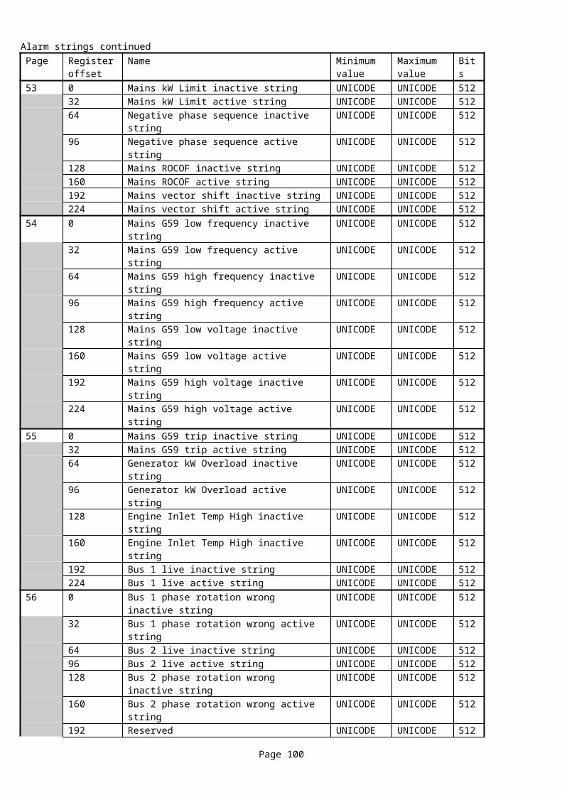
72xx/73xx family register allocation continued48-63 2130 Expansion module 1 digital inputs A-H raw & processed status64-79 2130 Expansion module 2 digital inputs A-H raw & processed status80-95 2130 Expansion module 3 digital inputs A-H raw & processed status96-191 Reserved for 2130 Expansion module 4-9 192 2130 Expansion module 0 analogue input E sender category 0 3 16193 2130 Expansion module 0 analogue input E input reading 16S194 2130 Expansion module 0 analogue input E sender category 0 3 16195 2130 Expansion module 0 analogue input E input reading 16S196 2130 Expansion module 0 analogue input F sender category 0 3 16197 2130 Expansion module 0 analogue input F input reading 16S198 2130 Expansion module 0 analogue input F sender category 0 3 16199 2130 Expansion module 0 analogue input F input reading 16S200 2130 Expansion module 0 analogue input G sender category 0 3 16201 2130 Expansion module 0 analogue input G input reading 16S202 2130 Expansion module 0 analogue input G sender category 0 3 16203 2130 Expansion module 0 analogue input G input reading 16S204 2130 Expansion module 0 analogue input H sender category 0 3 16205 2130 Expansion module 0 analogue input H input reading 16S206 2130 Expansion module 0 analogue input H sender category 0 3 16207 2130 Expansion module 0 analogue input H input reading 16S208-223 2130 Expansion module 1 inputs E-H224-239 2130 Expansion module 2 inputs E-H240-255 2130 Expansion module 3 inputs E-H
8xxx / 74xx family register allocationRegister offset
Name Min value Max value
Bits/ sign
0 Digital input A raw status 0 1 161 Digital input A processed status 0 1 162 Digital input B raw status 0 1 163 Digital input B processed status 0 1 164 Digital input C raw status 0 1 165 Digital input C processed status 0 1 166 Digital input D raw status 0 1 167 Digital input D processed status 0 1 168 Digital input E raw status 0 1 169 Digital input E processed status 0 1 1610 Digital input F raw status 0 1 1611 Digital input F processed status 0 1 1612 Digital input G raw status 0 1 1613 Digital input G processed status 0 1 1614 Digital input H raw status 0 1 1615 Digital input H processed status 0 1 1616 Digital input I raw status 0 1 1617 Digital input I processed status 0 1 1618 Digital input J raw status 0 1 1619 Digital input J processed status 0 1 1620 Digital input K raw status 0 1 1621 Digital input K processed status 0 1 1622 Digital input L raw status 0 1 1623 Digital input L processed status 0 1 1624 Digital input M raw status 0 1 1625 Digital input M processed status 0 1 1626 Digital input N raw status 0 1 1627 Digital input N processed status 0 1 1628 Digital input O raw status 0 1 1629 Digital input O processed status 0 1 1630 Digital input P raw status 0 1 1631 Digital input P processed status 0 1 16
Page 100
8xxx / 74xx family register allocation continued32 Digital input Q raw status 0 1 1633 Digital input Q processed status 0 1 1634 Digital input R raw status 0 1 1635 Digital input R processed status 0 1 1636 Digital input S raw status 0 1 1637 Digital input S processed status 0 1 1638 Digital input T raw status 0 1 1639 Digital input T processed status 0 1 1640 Digital input U raw status 0 1 1641 Digital input U processed status 0 1 1642 Digital input V raw status 0 1 1643 Digital input V processed status 0 1 1644 Digital input W raw status 0 1 1645 Digital input W processed status 0 1 1646 Digital input X raw status 0 1 1647 Digital input X processed status 0 1 1648 Digital input Y raw status 0 1 1649 Digital input Y processed status 0 1 1650 Digital input Z raw status 0 1 1651 Digital input Z processed status 0 1 1652 Digital input AA raw status 0 1 1653 Digital input AA processed status 0 1 1654 Digital input AB raw status 0 1 1655 Digital input AB processed status 0 1 1656 Digital input AC raw status 0 1 1657 Digital input AC processed status 0 1 1658 Digital input AD raw status 0 1 1659 Digital input AD processed status 0 1 1660 Digital input AE raw status 0 1 1661 Digital input AE processed status 0 1 1662 Digital input AF raw status 0 1 1663 Digital input AF processed status 0 1 1664 2130 Expansion module 0 digital input A raw status 0 1 1665 2130 Expansion module 0 digital input A processed status 0 1 1666 2130 Expansion module 0 digital input B raw status 0 1 1667 2130 Expansion module 0 digital input B processed status 0 1 1668 2130 Expansion module 0 digital input C raw status 0 1 1669 2130 Expansion module 0 digital input C processed status 0 1 1670 2130 Expansion module 0 digital input D raw status 0 1 1671 2130 Expansion module 0 digital input D processed status 0 1 1672 2130 Expansion module 0 digital input E raw status 0 1 1673 2130 Expansion module 0 digital input E processed status 0 1 1674 2130 Expansion module 0 digital input F raw status 0 1 1675 2130 Expansion module 0 digital input F processed status 0 1 1676 2130 Expansion module 0 digital input G raw status 0 1 1677 2130 Expansion module 0 digital input G processed status 0 1 1678 2130 Expansion module 0 digital input H raw status 0 1 1679 2130 Expansion module 0 digital input H processed status 0 1 1680-95 2130 Expansion module 1 digital inputs A-H status96-111 2130 Expansion module 2 digital inputs A-H status112-127 2130 Expansion module 3 digital inputs A-H status
Page 101
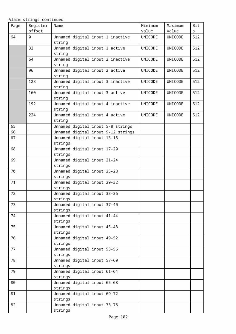
8xxx /74xx family register allocation continued128 2131Expansion module 0 digital input A raw status 0 1 16129 2131Expansion module 0 digital input A processed status 0 1 16130 2131Expansion module 0 digital input B raw status 0 1 16131 2131Expansion module 0 digital input B processed status 0 1 16132 2131Expansion module 0 digital input C raw status 0 1 16133 2131Expansion module 0 digital input C processed status 0 1 16134 2131Expansion module 0 digital input D raw status 0 1 16135 2131Expansion module 0 digital input D processed status 0 1 16136 2131Expansion module 0 digital input E raw status 0 1 16137 2131Expansion module 0 digital input E processed status 0 1 16138 2131Expansion module 0 digital input F raw status 0 1 16139 2131Expansion module 0 digital input F processed status 0 1 16140 2131Expansion module 0 digital input G raw status 0 1 16141 2131Expansion module 0 digital input G processed status 0 1 16142 2131Expansion module 0 digital input H raw status 0 1 16143 2131Expansion module 0 digital input H processed status 0 1 16144 2131Expansion module 0 digital input I raw status 0 1 16145 2131Expansion module 0 digital input I processed status 0 1 16146 2131Expansion module 0 digital input J raw status 0 1 16147 2131Expansion module 0 digital input J processed status 0 1 16148-167 2131Expansion module 1 digital inputs A-J status168-187 2131Expansion module 2 digital inputs A-J status188-207 2131Expansion module 3 digital inputs A-J status208-223 Reserved224 2130 Expansion module 0 analogue input E sender category 0 3 16225 2130 Expansion module 0 analogue input E input reading 16S226 2130 Expansion module 0 analogue input E sender category 0 3 16227 2130 Expansion module 0 analogue input E input reading 16S228 2130 Expansion module 0 analogue input F sender category 0 3 16229 2130 Expansion module 0 analogue input F input reading 16S230 2130 Expansion module 0 analogue input F sender category 0 3 16231 2130 Expansion module 0 analogue input F input reading 16S232 2130 Expansion module 0 analogue input G sender category 0 3 16233 2130 Expansion module 0 analogue input G input reading 16S234 2130 Expansion module 0 analogue input G sender category 0 3 16235 2130 Expansion module 0 analogue input G input reading 16S236 2130 Expansion module 0 analogue input H sender category 0 3 16237 2130 Expansion module 0 analogue input H input reading 16S238 2130 Expansion module 0 analogue input H sender category 0 3 16239 2130 Expansion module 0 analogue input H input reading 16S240-255 2130 Expansion module 1 analogue inputs E-H
Page 102
3xx family register allocationRegister offset
Name Min value
Max value
Bits/ sign
330
331
332
333
334
335
0 Digital input A raw status 0 1 16
1 Digital input A processed status 0 1 16
2 Digital input B raw status 0 1 16
3 Digital input B processed status 0 1 16
4 Digital input C raw status 0 1 16
5 Digital input C processed status 0 1 16
6 Digital input D raw status 0 1 16
7 Digital input D processed status 0 1 16
8 Digital input E raw status 0 1 16
9 Digital input E processed status 0 1 16
10 Digital input F raw status 0 1 16
11 Digital input F processed status 0 1 16
12 Digital input G raw status 0 1 16
13 Digital input G processed status 0 1 16
14 Digital input H raw status 0 1 16
15 Digital input H processed status 0 1 16
16 Digital input I raw status 0 1 16
17 Digital input I processed status 0 1 16
18 Digital input J raw status 0 1 16
19 Digital input J processed status 0 1 16
20 Digital input K raw status 0 1 16
21 Digital input K processed status 0 1 16
22 Digital input L raw status 0 1 16
23 Digital input L processed status 0 1 16
24-31 Unimplemented (reserved for future digital inputs)32 2130 Expansion module 0 digital input A raw status 0 1 16
33 2130 Expansion module 0 digital input A processed status 0 1 16
34 2130 Expansion module 0 digital input B raw status 0 1 16
35 2130 Expansion module 0 digital input B processed status 0 1 16
36 2130 Expansion module 0 digital input C raw status 0 1 16
37 2130 Expansion module 0 digital input C processed status 0 1 16
38 2130 Expansion module 0 digital input D raw status 0 1 16
39 2130 Expansion module 0 digital input D processed status 0 1 16
40 2130 Expansion module 0 digital input E raw status 0 1 16
41 2130 Expansion module 0 digital input E processed status 0 1 16
42 2130 Expansion module 0 digital input F raw status 0 1 16
43 2130 Expansion module 0 digital input F processed status 0 1 16
44 2130 Expansion module 0 digital input G raw status 0 1 16
45 2130 Expansion module 0 digital input G processed status 0 1 16
46 2130 Expansion module 0 digital input H raw status 0 1 16
47 2130 Expansion module 0 digital input H processed status 0 1 16
48-63 2130 Expansion module 1 digital inputs A-H status
64-79 Reserved for 2130 Expansion module 2 digital inputs A-H status)
80-95 Reserved for 2130 Expansion module 3 digital inputs A-H status)
96-191 Reserved for 2130 Expansion module 4-9192 2130 Expansion module 0 analogue input E sender category 0 3 16
193 2130 Expansion module 0 analogue input E input reading 16S
194 2130 Expansion module 0 analogue input E sender category 0 3 16
195 2130 Expansion module 0 analogue input E input reading 16S
196 2130 Expansion module 0 analogue input F sender category 0 3 16
197 2130 Expansion module 0 analogue input F input reading 16S
198 2130 Expansion module 0 analogue input F sender category 0 3 16
199 2130 Expansion module 0 analogue input F input reading 16S
Page 103
3xx family register allocation continuedRegister offset
Name Min value
Maxi value
Bits/ sign
330
331
332
333
334
335
200 2130 Expansion module 0 analogue input G sender category 0 3 16
201 2130 Expansion module 0 analogue input G input reading 16S
202 2130 Expansion module 0 analogue input G sender category 0 3 16
203 2130 Expansion module 0 analogue input G input reading 16S
204 2130 Expansion module 0 analogue input H sender category 0 3 16
205 2130 Expansion module 0 analogue input H input reading 16S
206 2130 Expansion module 0 analogue input H sender category 0 3 16
207 2130 Expansion module 0 analogue input H input reading 16S
208-223 2130 Expansion module 1 analogue inputs E-H
224-239 Reserved for 2130 Expansion module 2 analogue inputs E-H240-255 Reserved for 2130 Expansion module 3 analogue inputs E-H
Sender category codes and value rangesType code
Type Minimum value
Maximum value
Scaling factor
Units
0 Unused 0 01 Pressure 0 10000 1 KPa2 Temperature -200 10000 1 Degrees C3 Level 0 200 1 %4-65535 Reserved
Page 104
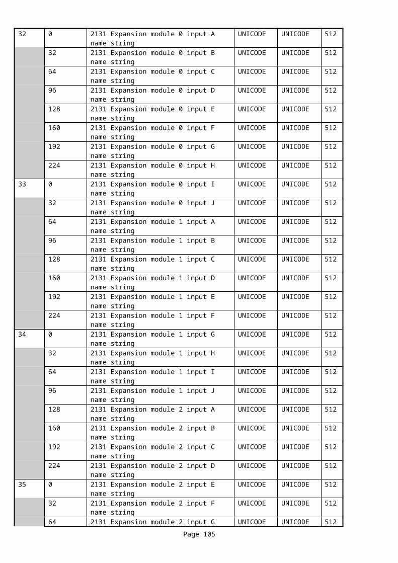
10.42 Page 171 – Unnamed input status continued
1. This page is a continuation of page 170; refer to that page for notes.2. Each family has different register allocations.3. These registers are Read-Only
72xx/73xx family register allocation continuedRegister offset
Name Minimum value
Maximum value
Bits/ sign
0-95 Reserved for 2130 Expansion module 4-9 inputs E-H96 Internal flexible sender analogue input sender category 0 1 1697 Internal flexible sender analogue input reading 0 1 1698 Internal flexible sender analogue input sender category 0 1 1699 Internal flexible sender analogue input reading 0 1 16100 Maintenance alarm 1 (raw) 0 1 16101 Maintenance alarm 1 (processed) 0 1 16102 Maintenance alarm 2 (raw) 0 1 16103 Maintenance alarm 2 (processed) 0 1 16104 Maintenance alarm 3 (raw) 0 1 16105 Maintenance alarm 3 (processed) 0 1 16106-255 Reserved
8xxx / 74xx family register allocation continuedRegister offset
Name Minimum value
Maximum value
Bits/ sign
0-15 2130 Expansion module 2 analogue inputs E-H16-31 2130 Expansion module 3 analogue inputs E-H32 2131 Expansion module 0 analogue input A sender category 0 3 1633 2131 Expansion module 0 analogue input A input reading 16S34 2131 Expansion module 0 analogue input B sender category 0 3 1635 2131 Expansion module 0 analogue input B input reading 16S36 2131 Expansion module 0 analogue input C sender category 0 3 1637 2131 Expansion module 0 analogue input C input reading 16S38 2131 Expansion module 0 analogue input D sender category 0 3 1639 2131 Expansion module 0 analogue input D input reading 16S40 2131 Expansion module 0 analogue input E sender category 0 3 1641 2131 Expansion module 0 analogue input E input reading 16S42 2131 Expansion module 0 analogue input F sender category 0 3 1643 2131 Expansion module 0 analogue input F input reading 16S44 2131 Expansion module 0 analogue input G sender category 0 3 1645 2131 Expansion module 0 analogue input G input reading 16S46 2131 Expansion module 0 analogue input H sender category 0 3 1647 2131 Expansion module 0 analogue input H input reading 16S48 2131 Expansion module 0 analogue input I sender category 0 3 1649 2131 Expansion module 0 analogue input I input reading 16S50 2131 Expansion module 0 analogue input J sender category 0 3 1651 2131 Expansion module 0 analogue input J input reading 16S52-71 2131 Expansion module 1 analogue inputs A-J72-91 2131 Expansion module 2 analogue inputs A-J92-111 2131 Expansion module 3 analogue inputs A-J112-127 Reserved
Page 105
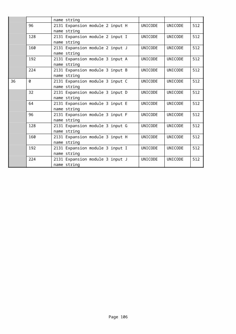
8xxx / 74xx family register allocation continued128 Internal flexible sender 1 analogue input sender category 0 1 16129 Internal flexible sender 1 analogue input reading 0 1 16130 Internal flexible sender 1 analogue input sender category 0 1 16131 Internal flexible sender 1 analogue input reading 0 1 16132 Internal flexible sender 2 analogue input sender category 0 1 16133 Internal flexible sender 2 analogue input reading 0 1 16134 Internal flexible sender 2 analogue input sender category 0 1 16135 Internal flexible sender 2 analogue input reading 0 1 16136 Internal flexible sender 3 analogue input sender category 0 1 16137 Internal flexible sender 3 analogue input reading 0 1 16138 Internal flexible sender 3 analogue input sender category 0 1 16139 Internal flexible sender 3 analogue input reading 0 1 16140 Internal flexible sender 4 analogue input sender category 0 1 16141 Internal flexible sender 4 analogue input reading 0 1 16142 Internal flexible sender 4 analogue input sender category 0 1 16143 Internal flexible sender 4 analogue input reading 0 1 16144 Internal flexible sender 5 analogue input sender category 0 1 16145 Internal flexible sender 5 analogue input reading 0 1 16146 Internal flexible sender 5 analogue input sender category 0 1 16147 Internal flexible sender 5 analogue input reading 0 1 16148 Maintenance alarm 1 (raw) 0 1 16149 Maintenance alarm 1 (processed) 0 1 16150 Maintenance alarm 2 (raw) 0 1 16151 Maintenance alarm 2 (processed) 0 1 16152 Maintenance alarm 3 (raw) 0 1 16153 Maintenance alarm 3 (processed) 0 1 16154 PLC alarm 1 trigger 16155 PLC alarm 1 condition 16156 PLC alarm 2 trigger 16157 PLC alarm 2 condition 16158 PLC alarm 3 trigger 16159 PLC alarm 3 condition 16160 PLC alarm 4 trigger 16161 PLC alarm 4 condition 16162 PLC alarm 5 trigger 16163 PLC alarm 5 condition 16164 PLC alarm 6 trigger 16165 PLC alarm 6 condition 16166 PLC alarm 7 trigger 16167 PLC alarm 7 condition 16168 PLC alarm 8 trigger 16169 PLC alarm 8 condition 16170 PLC alarm 9 trigger 16171 PLC alarm 9 condition 16172 PLC alarm 10 trigger 16173 PLC alarm 10 condition 16174 PLC alarm 11 trigger 16175 PLC alarm 11 condition 16176 PLC alarm 12 trigger 16177 PLC alarm 12 condition 16178 PLC alarm 13 trigger 16179 PLC alarm 13 condition 16180 PLC alarm 14 trigger 16181 PLC alarm 14 condition 16182 PLC alarm 15 trigger 16183 PLC alarm 15 condition 16184 PLC alarm 16 trigger 16185 PLC alarm 16 condition 16
Page 106
8xxx / 74xx family register allocation continued186 PLC alarm 17 trigger 16187 PLC alarm 17 condition 16188 PLC alarm 18 trigger 16189 PLC alarm 18 condition 16190 PLC alarm 19 trigger 16191 PLC alarm 19 condition 16192 PLC alarm 20 trigger 16193 PLC alarm 20 condition 16194 2133 Expansion module 0 analogue input A input reading 16S195 2133 Expansion module 0 analogue input B input reading 16S196 2133 Expansion module 0 analogue input C input reading 16S197 2133 Expansion module 0 analogue input D input reading 16S198 2133 Expansion module 0 analogue input E input reading 16S199 2133 Expansion module 0 analogue input F input reading 16S200 2133 Expansion module 0 analogue input G input reading 16S201 2133 Expansion module 0 analogue input H input reading 16S202-209 2133 Expansion module 1 analogue inputs A-H input readings 16S210-217 2133 Expansion module 2 analogue inputs A-H input readings 16S218-225 2133 Expansion module 3 analogue inputs A-H input readings 16S226-255 Reserved
Page 107

3xx family register allocation continuedRegister offset
Name Minimum value
Maximum value
Bits/ sign
330
331
332
333
334
335
0-95 Reserved for 2130 Expansion modules 4-9analogue inputs E-H96 PLC alarm 1 trigger 16
97 PLC alarm 1 condition 16
98 PLC alarm 2 trigger 16
99 PLC alarm 2 condition 16
100 PLC alarm 3 trigger 16
101 PLC alarm 3 condition 16
102 PLC alarm 4 trigger 16
103 PLC alarm 4 condition 16
104 PLC alarm 5 trigger 16
105 PLC alarm 5 condition 16
106 PLC alarm 6 trigger 16
107 PLC alarm 6 condition 16
108 PLC alarm 7 trigger 16
109 PLC alarm 7 condition 16
110 PLC alarm 8 trigger 16
111 PLC alarm 8 condition 16
112 PLC alarm 9 trigger 16
113 PLC alarm 9 condition 16
114 PLC alarm 10 trigger 16
115 PLC alarm 10 condition 16
116 PLC alarm 11 trigger 16
117 PLC alarm 11 condition 16
118 PLC alarm 12 trigger 16
119 PLC alarm 12 condition 16
120 PLC alarm 13 trigger 16
121 PLC alarm 13 condition 16
122 PLC alarm 14 trigger 16
123 PLC alarm 14 condition 16
124 PLC alarm 15 trigger 16
125 PLC alarm 15 condition 16
126 PLC alarm 16 trigger 16
127 PLC alarm 16 condition 16
3xx family register allocation continuedRegister offset
Name Minimum value
Maximum value
Bits/ sign
330
331
332
333
334
335
128 PLC alarm 17 trigger 16
129 PLC alarm 17 condition 16
130 PLC alarm 18 trigger 16
131 PLC alarm 18 condition 16
132 PLC alarm 19 trigger 16
133 PLC alarm 19 condition 16
134 PLC alarm 20 trigger 16
135 PLC alarm 20 condition 16
136-255 Reserved
Page 108

10.43 Page 180 – Unnamed output sources & polarities
1. This page indicates the control source and polarity settings for every digital output and LED, taken directly from the configuration.
2. Each family has different register allocations for registers 0-63 but common ones for the remainder of the page.3. This is continued on page 181.4. These registers are Read-Only
72xx/73xx family register allocations 0-63Register offset
Name Minimum value
Maximum value
Bits/ sign
Read/write
0 Digital output A source (Fuel) 0 65535 16 Read only1 Digital output A polarity (Fuel) 0 1 16 Read only2 Digital output B source (Crank) 0 65535 16 Read only3 Digital output B polarity (Crank) 0 1 16 Read only4 Digital output E source 0 65535 16 Read only5 Digital output E polarity 0 1 16 Read only6 Digital output F source 0 65535 16 Read only7 Digital output F polarity 0 1 16 Read only8 Digital output G source 0 65535 16 Read only9 Digital output G polarity 0 1 16 Read only10 Digital output H source 0 65535 16 Read only11 Digital output H polarity 0 1 16 Read only12 Digital output D source (Generator) 0 65535 16 Read only13 Digital output D polarity (Generator) 0 1 16 Read only14 Digital output C source (Mains) 0 65535 16 Read only15 Digital output C polarity (Mains) 0 1 16 Read only16 STOP LED source (STOP) 0 65535 16 Read only17 STOP LED polarity (STOP) 0 1 16 Read only18 MANUAL LED source (MANUAL) 0 65535 16 Read only19 MANUAL LED polarity (MANUAL) 0 1 16 Read only20 TEST LED source (TEST) 0 65535 16 Read only21 TEST LED polarity (TEST) 0 1 16 Read only22 AUTO LED source (AUTO) 0 65535 16 Read only23 AUTO LED polarity (AUTO) 0 1 16 Read only24 MAINS LED source (MAINS) 0 65535 16 Read only25 MAINS LED polarity (MAINS) 0 1 16 Read only26 MAINS BREAKER LED source (MAINS BREAKER) 0 65535 16 Read only27 MAINS BREAKER LED polarity (MAINS BREAKER) 0 1 16 Read only28 GEN BREAKER LED source (GEN BREAKER) 0 65535 16 Read only29 GEN BREAKER LED polarity (GEN BREAKER) 0 1 16 Read only30 GEN LED source (GEN) 0 65535 16 Read only31 GEN LED polarity (GEN) 0 1 16 Read only32 USER LED 1 source (USER LED 1) 0 65535 16 Read only33 USER LED 1 polarity (USER LED 1) 0 1 16 Read only34 USER LED 2 source (USER LED 2) 0 65535 16 Read only35 USER LED 2 polarity (USER LED 2) 0 1 16 Read only36 USER LED 3 source (USER LED 3) 0 65535 16 Read only37 USER LED 3 polarity (USER LED 3) 0 1 16 Read only38 USER LED 4 source (USER LED 4) 0 65535 16 Read only39 USER LED 4 polarity (USER LED 4) 0 1 16 Read only40-63 Reserved
Page 109

8xxx /74xx family register allocations 0-63Register offset
Name Minimum value
Maximum value
Bits/ sign
Read/write
0 Digital output A source (Fuel) 0 65535 16 Read only1 Digital output A polarity (Fuel) 0 1 16 Read only2 Digital output B source (Crank) 0 65535 16 Read only3 Digital output B polarity (Crank) 0 1 16 Read only4 Digital output E source 0 65535 16 Read only5 Digital output E polarity 0 1 16 Read only6 Digital output F source 0 65535 16 Read only7 Digital output F polarity 0 1 16 Read only8 Digital output G source 0 65535 16 Read only9 Digital output G polarity 0 1 16 Read only10 Digital output H source 0 65535 16 Read only11 Digital output H polarity 0 1 16 Read only12 Digital output I source 0 65535 16 Read only13 Digital output I polarity 0 1 16 Read only14 Digital output J source 0 65535 16 Read only15 Digital output J polarity 0 1 16 Read only16 Digital output K source 0 65535 16 Read only17 Digital output K polarity 0 1 16 Read only18 Digital output L source 0 65535 16 Read only19 Digital output L polarity 0 1 16 Read only20 Digital output M source 0 65535 16 Read only21 Digital output M polarity 0 1 16 Read only22 Digital output N source 0 65535 16 Read only23 Digital output N polarity 0 1 16 Read only24 Digital output D source (Generator) 0 65535 16 Read only25 Digital output D polarity (Generator) 0 1 16 Read only26 Digital output C source (Mains) 0 65535 16 Read only27 Digital output C polarity (Mains) 0 1 16 Read only28 STOP LED source (STOP) 0 65535 16 Read only29 STOP LED polarity (STOP) 0 1 16 Read only30 MANUAL LED source (MANUAL) 0 65535 16 Read only31 MANUAL LED polarity (MANUAL) 0 1 16 Read only32 TEST LED source (TEST) 0 65535 16 Read only33 TEST LED polarity (TEST) 0 1 16 Read only34 AUTO LED source (AUTO) 0 65535 16 Read only35 AUTO LED polarity (AUTO) 0 1 16 Read only36 MAINS LED source (MAINS) 0 65535 16 Read only37 MAINS LED polarity (MAINS) 0 1 16 Read only38 MAINS BREAKER LED source (MAINS BREAKER) 0 65535 16 Read only39 MAINS BREAKER LED polarity (MAINS BREAKER) 0 1 16 Read only40 GEN BREAKER LED source (GEN BREAKER) 0 65535 16 Read only41 GEN BREAKER LED polarity (GEN BREAKER) 0 1 16 Read only42 GEN LED source (GEN) 0 65535 16 Read only43 GEN LED polarity (GEN) 0 1 16 Read only44 USER LED 1 source (USER LED 1) 0 65535 16 Read only45 USER LED 1 polarity (USER LED 1) 0 1 16 Read only46 USER LED 2 source (USER LED 2) 0 65535 16 Read only47 USER LED 2 polarity (USER LED 2) 0 1 16 Read only48 USER LED 3 source (USER LED 3) 0 65535 16 Read only49 USER LED 3 polarity (USER LED 3) 0 1 16 Read only50 USER LED 4 source (USER LED 4) 0 65535 16 Read only51 USER LED 4 polarity (USER LED 4) 0 1 16 Read only52-63 Reserved
Page 110
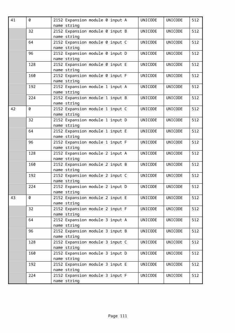
332/333 register allocationRegister offset
Name Minimum value
Maximum value
Bits/ sign Read/write
0 Mains breaker output source 0 65535 16 Read only1 Mains breaker output polarity 0 1 16 Read only2 Generator breaker output source 0 65535 16 Read only3 Generator breaker output polarity 0 1 16 Read only4 Digital output C source 0 65535 16 Read only5 Digital output C polarity 0 1 16 Read only6 Digital output D source 0 65535 16 Read only7 Digital output D polarity 0 1 16 Read only8 Digital output E source 0 65535 16 Read only9 Digital output E polarity 0 1 16 Read only10-15 Reserved for future outputs16 Exercise LED source 0 65535 16 Read only17 Exercise LED polarity 0 1 16 Read only18 Manual LED source 0 65535 16 Read only19 Manual LED source 0 1 16 Read only20 Prohibit Return LED source 0 65535 16 Read only21 Prohibit Return LED source 0 1 16 Read only22 Auto LED source 0 65535 16 Read only23 Auto LED source 0 1 16 Read only24 Generator breaker LED source 0 65535 16 Read only25 Generator breaker LED source 0 1 16 Read only26 Mains breaker LED source 0 65535 16 Read only27 Mains breaker LED source 0 1 16 Read only28 Generator available LED source 0 65535 16 Read only29 Generator available LED source 0 1 16 Read only28 Mains available LED source 0 65535 16 Read only29 Mains available LED source 0 1 16 Read only28 Warning LED source 0 65535 16 Read only29 Warning LED polarity 0 1 16 Read only30 LCD Indicator 1 source (USER LED 1) 0 65535 16 Read only31 LCD Indicator 1 polarity (USER LED 1) 0 1 16 Read only32 LCD Indicator 2 source (USER LED 2) 0 65535 16 Read only33 LCD Indicator 2 polarity (USER LED 2) 0 1 16 Read only34 LCD Indicator 3 source (USER LED 3) 0 65535 16 Read only35 LCD Indicator 3 polarity (USER LED 3) 0 1 16 Read only36-63 Reserved
Page 111
330/331/334 Register allocations 0 - 63Register offset
Name Minimum value
Maximum value
Bits/ sign 330
331
334
0 Digital output A source 0 65535 16
1 Digital output A polarity 0 1 16
2 Digital output B source 0 65535 16
3 Digital output B polarity 0 1 16
4 Digital output C source 0 65535 16
5 Digital output C polarity 0 1 16
6 Digital output D source 0 65535 16
7 Digital output D polarity 0 1 16
8 Digital output E source 0 65535 16
9 Digital output E polarity 0 1 16
10 Digital output F source 0 65535 16
11 Digital output F polarity 0 1 16
12 Digital output G source 0 65535 16
13 Digital output G polarity 0 1 16
14 Digital output H source 0 65535 16
15 Digital output H polarity 0 1 16
16 Stop LED source 0 65535 16
17 Stop LED polarity 0 1 16
18 Manual LED source 0 65535 16
19 Manual LED polarity 0 1 16
20 Auto LED source 0 65535 16
21 Auto LED polarity 0 1 16
22 Mode LED source 0 65535 16
23 Mode LED polarity 0 1 16
24 S2 breaker LED source 0 65535 16
25 S2 breaker LED polarity 0 1 16
26 S1breaker LED source 0 65535 16
27 S1 breaker LED polarity 0 1 16
28 S2 available LED source 0 65535 16
29 S2 available LED polarity 0 1 16
30 S1 available LED source 0 65535 16
31 S1 available LED polarity 0 1 16
32 Warning LED source 0 65535 16
33 Warning LED polarity 0 1 16
34 USER LED / LCD Indicator 1 source (USER LED 1) 0 65535 16
35 USER LED / LCD Indicator 1 polarity (USER LED 1)
0 1 16
36 USER LED / LCD Indicator 2 source (USER LED 2) 0 65535 16
37 USER LED / LCD Indicator 2 polarity (USER LED 2)
0 1 16
38 USER LED / LCD Indicator 3 source (USER LED 3) 0 65535 16
39 USER LED / LCD Indicator 3 polarity (USER LED 3)
0 1 16
40-63 Reserved
Page 112
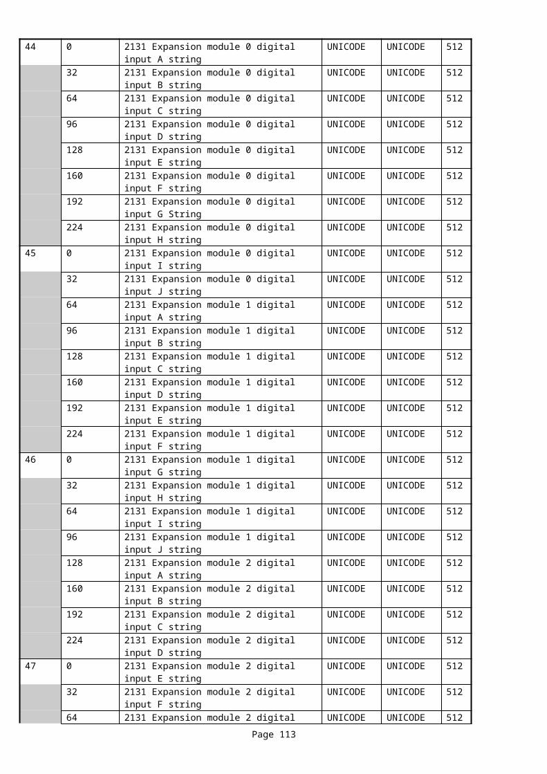
335 Register allocations 0 - 63Register offset
Name Minimum value
Maximum value
Bits/ sign Read/write
0 Digital output A source 0 65535 16 Read only1 Digital output A polarity 0 1 16 Read only2 Digital output B source 0 65535 16 Read only3 Digital output B polarity 0 1 16 Read only4 Digital output C source 0 65535 16 Read only5 Digital output C polarity 0 1 16 Read only6 Digital output D source 0 65535 16 Read only7 Digital output D polarity 0 1 16 Read only8 Digital output E source 0 65535 16 Read only9 Digital output E polarity 0 1 16 Read only10 Digital output F source 0 65535 16 Read only11 Digital output F polarity 0 1 16 Read only12 Digital output G source 0 65535 16 Read only13 Digital output G polarity 0 1 16 Read only14 Digital output H source 0 65535 16 Read only15 Digital output H polarity 0 1 16 Read only16 Digital output I source 0 65535 16 Read only17 Digital output I polarity 0 1 16 Read only18 Digital output J source 0 65535 16 Read only19 Digital output J polarity 0 1 16 Read only20 Digital output K source 0 65535 16 Read only21 Digital output K polarity 0 1 16 Read only22 Digital output L source 0 65535 16 Read only23 Digital output L polarity 0 1 16 Read only24 Stop LED source 0 65535 16 Read only25 Stop LED polarity 0 1 16 Read only26 Manual LED source 0 65535 16 Read only27 Manual LED polarity 0 1 16 Read only28 Mode LED source 0 65535 16 Read only29 Mode LED polarity 0 1 16 Read only30 Auto LED source 0 65535 16 Read only31 Auto LED polarity 0 1 16 Read only32 S2 breaker LED source 0 65535 16 Read only33 S2 breaker LED polarity 0 1 16 Read only34 S1breaker LED source 0 65535 16 Read only35 S1 breaker LED polarity 0 1 16 Read only36 S2 available LED source 0 65535 16 Read only37 S2 available LED polarity 0 1 16 Read only38 S1 available LED source 0 65535 16 Read only39 S1 available LED polarity 0 1 16 Read only40 USER LED 1 source 0 65535 16 Read only41 USER LED 1 polarity 0 1 16 Read only42 USER LED 2 source 0 65535 16 Read only43 USER LED 2 polarity 0 1 16 Read only44 USER LED 3 source 0 65535 16 Read only45 USER LED 3 polarity 0 1 16 Read only46 USER LED 4 source 0 65535 16 Read only47 USER LED 4 polarity 0 1 16 Read only48 USER LED 1 colour 0 1 16 Read only49 USER LED 2 colour 0 1 16 Read only50 USER LED 3 colour 0 1 16 Read only51 USER LED 4 colour 0 1 16 Read only52-63 Reserved
Page 113
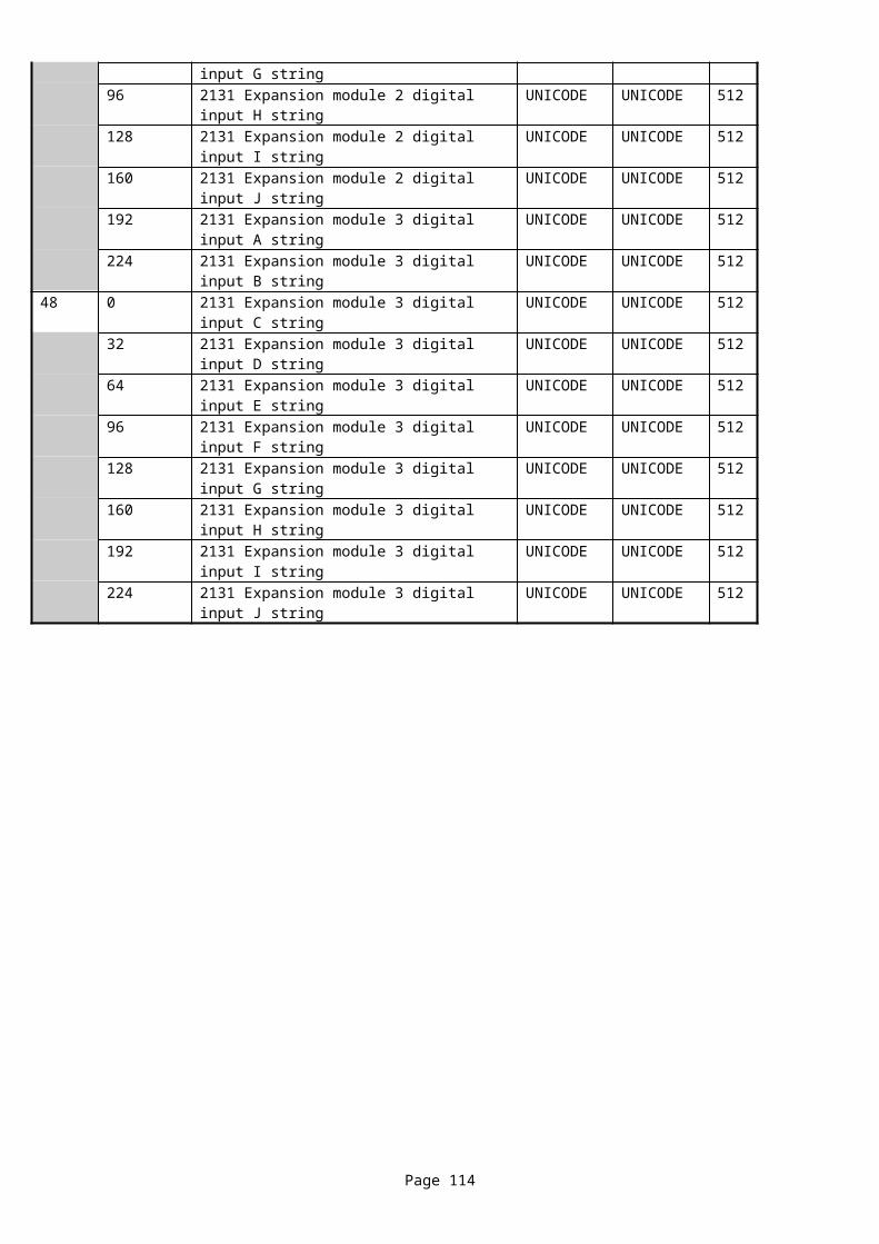
8xxx/74xx/72xx/73xx/3xx Common family register allocations 64-255 Register offset
Name Minimum value
Maximum value
Bits/ sign
8xxx/ 74xx
72xx/73xx
335
64 2157 expansion module 0 output A source 0 65535 16
65 2157 expansion module 0 output A polarity 0 1 16
66 2157 expansion module 0 output B source 0 65535 16
67 2157 expansion module 0 output B polarity 0 1 16
68 2157 expansion module 0 output C source 0 65535 16
69 2157 expansion module 0 output C polarity 0 1 16
70 2157 expansion module 0 output D source 0 65535 16
71 2157 expansion module 0 output D polarity 0 1 16
72 2157 expansion module 0 output E source 0 65535 16
73 2157 expansion module 0 output E polarity 0 1 16
74 2157 expansion module 0 output F source 0 65535 16
75 2157 expansion module 0 output F polarity 0 1 16
76 2157 expansion module 0 output G source 0 65535 16
77 2157 expansion module 0 output G polarity 0 1 16
78 2157 expansion module 0 output H source 0 65535 16
79 2157 expansion module 0 output H polarity 0 1 16
80-95 2157 expansion module 1 outputs A-H 0 65535 16
96-111 2157 expansion module 2 outputs A-H 0 1 16
112-127 2157 expansion module 3 outputs A-H 0 65535 16
128-223 2157 expansion module 4-9 outputs A-H 0 1 16
224 2548 expansion module 0 output A source 0 65535 16
225 2548 expansion module 0 output A polarity 0 1 16
226 2548 expansion module 0 output B source 0 65535 16
227 2548 expansion module 0 output B polarity 0 1 16
228 2548 expansion module 0 output C source 0 65535 16
229 2548 expansion module 0 output C polarity 0 1 16
230 2548 expansion module 0 output D source 0 65535 16
231 2548 expansion module 0 output D polarity 0 1 16
232 2548 expansion module 0 output E source 0 65535 16
233 2548 expansion module 0 output E polarity 0 1 16
234 2548 expansion module 0 output F source 0 65535 16
235 2548 expansion module 0 output F polarity 0 1 16
236 2548 expansion module 0 output G source 0 65535 16
237 2548 expansion module 0 output G polarity 0 1 16
238 2548 expansion module 0 output H source 0 65535 16
239 2548 expansion module 0 output H polarity 0 1 16
240 2548 expansion module 0 sounder output Source 0 65535 16
241 2548 expansion module 0 sounder output polarity 0 1 16
242-255 2548 expansion module 1 outputs A-G
LED coloursType code
Type
0 Red1 Green
Page 114
10.44 Page 181 – Unnamed output sources & polarities continued
1. This page is a continuation of page 180; refer to that page for notes.
8xxx/74xx/72xx/73xx/3xx Common family register allocations 0-255 continuedRegister offset
Name Minimum value
Maximum value
Bits/ sign
8xxx/ 74xx
72xx/73xx
335
0 2548 expansion module 1 output H source 0 65535 16
1 2548 expansion module 1 output H polarity 0 1 16
2 2548 expansion module 1 sounder output Source 0 65535 16
3 2548 expansion module 1 sounder output polarity 0 1 16
4-21 2548 expansion module 2 outputs A-H & sounder
22-39 2548 expansion module 3 outputs A-H & sounder
40-57 2548 expansion module 4 outputs A-H & sounder
58-75 2548 expansion module 5 outputs A-H & sounder
76-93 2548 expansion module 6 outputs A-H & sounder
94-111 2548 expansion module 7 outputs A-H & sounder
112-129 2548 expansion module 8 outputs A-H & sounder
130-147 2548 expansion module 9 outputs A-H & sounder
148-255 Reserved
Page 115
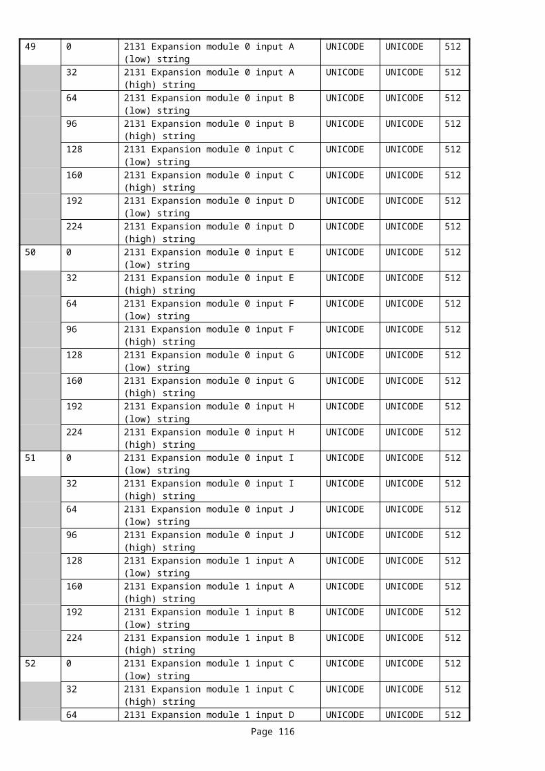
10.45 Page 182 – Virtual output sources & polarities
1. This page indicates the control source and polarity settings for every virtual output, taken directly from the configuration.
RegistersRegister offset
Name Minimum value
Maximum value
Scaling factor
Units Bits/ sign Read/write
0 Virtual output 1 source 0 65535 16 Read only1 Virtual output 1 polarity 0 1 16 Read only2 Virtual output 2 source 0 65535 16 Read only3 Virtual output 2 polarity 0 1 16 Read only4 Virtual output 3 source 0 65535 16 Read only5 Virtual output 3 polarity 0 1 16 Read only6 Virtual output 4 source 0 65535 16 Read only7 Virtual output 4 polarity 0 1 16 Read only8 Virtual output 5 source 0 65535 16 Read only9 Virtual output 5 polarity 0 1 16 Read only10 Virtual output 6 source 0 65535 16 Read only11 Virtual output 6 polarity 0 1 16 Read only12 Virtual output 7 source 0 65535 16 Read only13 Virtual output 7 polarity 0 1 16 Read only14 Virtual output 8 source 0 65535 16 Read only15 Virtual output 8 polarity 0 1 16 Read only16 Virtual output 9 source 0 65535 16 Read only17 Virtual output 9 polarity 0 1 16 Read only18 Virtual output 10 source 0 65535 16 Read only19 Virtual output 10 polarity 0 1 16 Read only20 Virtual output 11 source 0 65535 16 Read only21 Virtual output 11 polarity 0 1 16 Read only22 Virtual output 12 source 0 65535 16 Read only23 Virtual output 12 polarity 0 1 16 Read only24 Virtual output 13 source 0 65535 16 Read only25 Virtual output 13 polarity 0 1 16 Read only26 Virtual output 14 source 0 65535 16 Read only27 Virtual output 14 polarity 0 1 16 Read only28 Virtual output 15 source 0 65535 16 Read only29 Virtual output 15 polarity 0 1 16 Read only30 Virtual output 16 source 0 65535 16 Read only31 Virtual output 16 polarity 0 1 16 Read only32 Virtual output 17 source 0 65535 16 Read only33 Virtual output 17 polarity 0 1 16 Read only34 Virtual output 18 source 0 65535 16 Read only35 Virtual output 18 polarity 0 1 16 Read only36 Virtual output 19 source 0 65535 16 Read only37 Virtual output 19 polarity 0 1 16 Read only38 Virtual output 20 source 0 65535 16 Read only39 Virtual output 20 polarity 0 1 16 Read only40-255 Reserved
Page 116
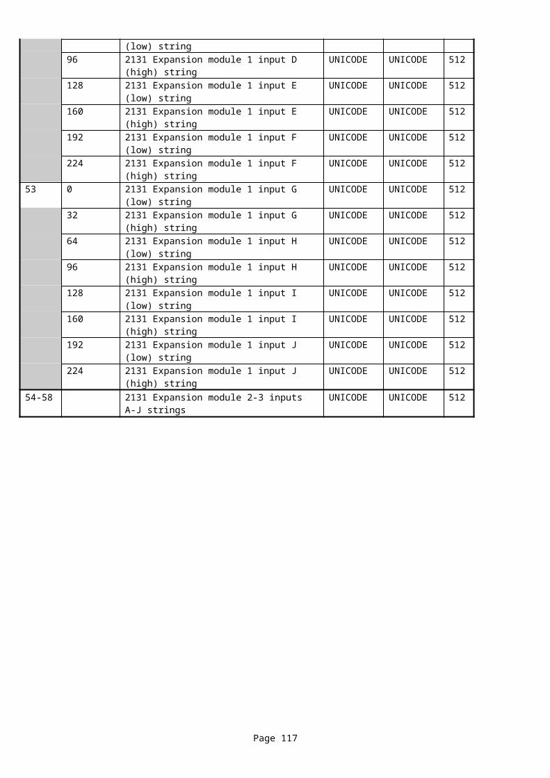
10.46 Page 183 – Configurable output sources & polarities
1. This page indicates the control source and polarity settings for every configurable output, taken directly from the configuration.
RegistersRegister offset
Name Minimum value
Maximum value
Scaling factor
Units Bits/ sign Read/write
0 configurable output 1 item A source 0 65535 16 Read only1 configurable output 1 item A polarity 0 1 16 Read only2 configurable output 1 item B source 0 65535 16 Read only3 configurable output 1 item B polarity 0 1 16 Read only4 configurable output 1 item C source 0 65535 16 Read only5 configurable output 1 item C polarity 0 1 16 Read only6 configurable output 2 item A source 0 65535 16 Read only7 configurable output 2 item A polarity 0 1 16 Read only8 configurable output 2 item B source 0 65535 16 Read only9 configurable output 2 item B polarity 0 1 16 Read only10 configurable output 2 item C source 0 65535 16 Read only11 configurable output 2 item C polarity 0 1 16 Read only12 configurable output 3 item A source 0 65535 16 Read only13 configurable output 3 item A polarity 0 1 16 Read only14 configurable output 3 item B source 0 65535 16 Read only15 configurable output 3 item B polarity 0 1 16 Read only16 configurable output 3 item C source 0 65535 16 Read only17 configurable output 3 item C polarity 0 1 16 Read only18-255 Reserved
Page 117
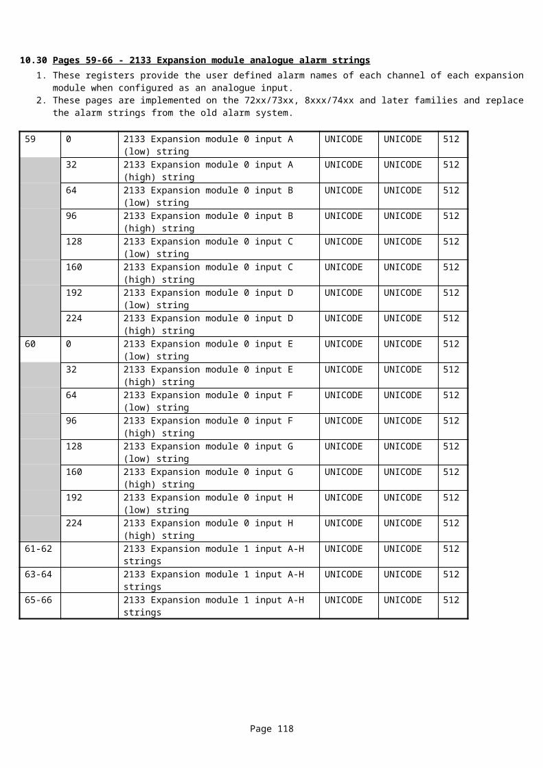
10.47 Page 184 – Analogue output sources, types and values
1. The analogue output source list is the same as the list in the expansion configuration and is not duplicated here.2. The analogue output type is described in the table below.3. The analogue output value for an output configured for voltage is in millivolts.4. The analogue output value for an output configured for current is in microamps but should be displayed in milliamps.
RegistersRegister offset
Name Minimum value
Maximum value
Bits/ sign Read/write
0 2152 expansion module 0 analogue output A source 0 65535 16 Read only1 2152 expansion module 0 analogue output A type 0 1 16 Read only2 2152 expansion module 0 analogue output B source 0 65535 16 Read only3 2152 expansion module 0 analogue output B type 0 1 16 Read only4 2152 expansion module 0 analogue output C source 0 65535 16 Read only5 2152 expansion module 0 analogue output C type 0 1 16 Read only6 2152 expansion module 0 analogue output D source 0 65535 16 Read only7 2152 expansion module 0 analogue output D type 0 1 16 Read only8 2152 expansion module 0 analogue output E source 0 65535 16 Read only9 2152 expansion module 0 analogue output E type 0 1 16 Read only10 2152 expansion module 0 analogue output F source 0 65535 16 Read only11 2152 expansion module 0 analogue output F type 0 1 16 Read only12-23 2152 expansion module 1 analogue outputs A-F Read only24-35 2152 expansion module 2 analogue outputs A-F Read only36-47 2152 expansion module 3 analogue outputs A-F Read only48 2152 expansion module 0 analogue output A value See table below 16S Read only49 2152 expansion module 0 analogue output B value See table below 16S Read only50 2152 expansion module 0 analogue output C value See table below 16S Read only51 2152 expansion module 0 analogue output D value See table below 16S Read only52 2152 expansion module 0 analogue output E value See table below 16S Read only53 2152 expansion module 0 analogue output F value See table below 16S Read only54-59 2152 expansion module 1 analogue outputs A-F value Read only60-65 2152 expansion module 2 analogue outputs A-F value Read only66-71 2152 expansion module 3 analogue outputs A-F value Read only72-255 Reserved
Output types and value rangesType code
Type Minimum value
Maximum value
Scaling factor
Units
0 Voltage 0 10000 0.001 V1 Current 0 20000 0.001 mA2-65535 Reserved
Page 118
10.48 Page 190 – Unnamed output status
1. This page indicates the current status of each output from the module, both digital outputs and LEDs.2. LED outputs are affected by lamp test.3. LED and button allocations vary by model and are shown in the table below.4. Each family has different allocations for registers 0-31 but common ones for the remainder of the page.5. These registers are Read-Only6. Unimplemented registers within a family/module are shaded.
72xx/73xx family register allocation 0-31Register offset
Name Minimum value
Maximum value
Bits/ sign
0 Digital output A status (Fuel) 0 1 161 Digital output B status (Crank) 0 1 162 Digital output E status 0 1 163 Digital output F status 0 1 164 Digital output G status 0 1 165 Digital output H status 0 1 166 Digital output D status (Gen) 0 1 167 Digital output C status (Mains) 0 1 168 STOP LED status(STOP) 0 1 169 MANUAL LED status (MANUAL) 0 1 1610 TEST LED status (TEST) 0 1 1611 AUTO LED status (AUTO) 0 1 1612 MAINS LED status (MAINS) 0 1 1613 MAINS BREAKER LED status (MAINS
BREAKER)0 1 16
14 GEN BREAKER LED status (GEN BREAKER) 0 1 1615 GEN LED status (GEN) 0 1 1616 USER LED 1 status (USER LED 1) 0 1 1617 USER LED 2 status (USER LED 2) 0 1 1618 USER LED 3 status (USER LED 3) 0 1 1619 USER LED 4 status (USER LED 4) 0 1 1620-31 Reserved
332/333 register allocation 0-31Register offset
Name Minimum value
Maximum value
Bits/ sign
0 Digital output A 0 1 161 Digital output B 0 1 162 Digital output C 0 1 163 Digital output D 0 1 164 Digital output E 0 1 165-15 Reserved for future outputs 0 1 1616 Exercise LED 0 1 1617 Manual LED 0 1 1618 Prohibit Return LED 0 1 1619 Auto LED 0 1 1620 Generator breaker LED 0 1 1621 Mains breaker LED 0 1 1622 Generator available LED 0 1 1623 Mains available LED 0 1 1624 Warning LED 0 1 1625 LCD Indicator 1 (USER LED 1) 0 1 1626 LCD Indicator 2 (USER LED 2) 0 1 1627 LCD Indicator 3 (USER LED 3) 0 1 1628-31 Reserved
Page 119
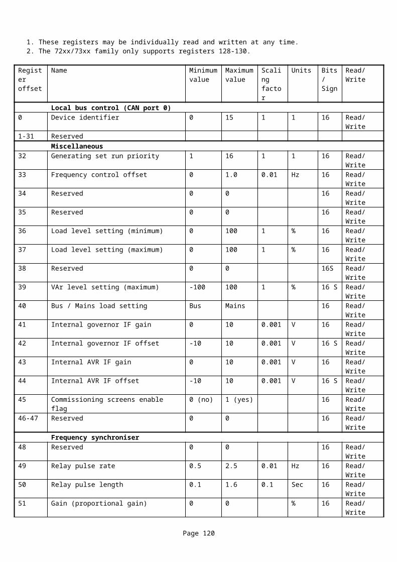
330/331/334 register allocation 0-31Register offset
Name Minimum value
Maximum value
Bits/ sign 330
331
334
0 Digital output A 0 1 16
1 Digital output B 0 1 16
2 Digital output C 0 1 16
3 Digital output D 0 1 16
4 Digital output E 0 1 16
5 Digital output F 0 1 16
6 Digital output G 0 1 16
7 Digital output H 0 1 16
8-15 Unimplemented - Reserved for future outputs 0 1 1616 Stop LED 0 1 16
17 Manual LED 0 1 16
18 Mode LED 0 1 16
19 Auto LED 0 1 16
20 S2 breaker LED 0 1 16
21 S1 breaker LED 0 1 16
22 S2 available LED 0 1 16
23 S1 available LED 0 1 16
24 Warning LED 0 1 16
25 USER / LCD Indicator 1 (USER LED 1) 0 1 16
26 USER / LCD Indicator 2 (USER LED 2) 0 1 16
27 USER / LCD Indicator 3 (USER LED 3) 0 1 16
28-31 Reserved
335 register allocation 0-31Register offset
Name Minimum value
Maximum value
Bits/ sign
0 Digital output A status 0 1 161 Digital output B status 0 1 162 Digital output C status 0 1 163 Digital output D status 0 1 164 Digital output E status 0 1 165 Digital output F status 0 1 166 Digital output G status 0 1 167 Digital output H status 0 1 168 Digital output I status 0 1 169 Digital output J status 0 1 1610 Digital output K status 0 1 1611 Digital output L status 0 1 1612-15 Unimplemented - Reserved for future outputs 0 1 1616 Stop LED 0 1 1617 Manual LED 0 1 1618 Mode LED 0 1 1619 Auto LED 0 1 1620 S2 breaker LED 0 1 1621 S1 breaker LED 0 1 1622 S2 available LED 0 1 1623 S1 available LED 0 1 1624 USER LED 1 0 1 1625 USER LED 2 0 1 1626 USER LED 3 0 1 1627 USER LED 4 0 1 1628-31 Reserved
Page 120
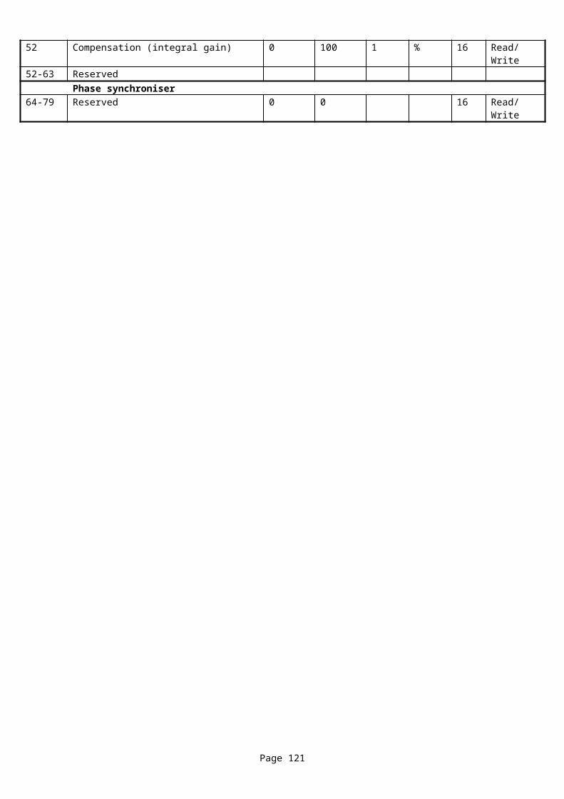
8xxx / 74xx family register allocation 0-255Register offset
Name Minimum value
Maximum value
Bits/ sign
0 Digital output A status (Fuel) 0 1 161 Digital output B status (Crank) 0 1 162 Digital output E status 0 1 163 Digital output F status 0 1 164 Digital output G status 0 1 165 Digital output H status 0 1 166 Digital output I status 0 1 167 Digital output J status 0 1 168 Digital output K status 0 1 169 Digital output L status 0 1 1610 Digital output M status 0 1 1611 Digital output N status 0 1 1612 Digital output D status (Gen) 0 1 1613 Digital output C status (Mains) 0 1 1614 STOP LED status(STOP) 0 1 1615 MANUAL LED status (MANUAL) 0 1 1616 TEST LED status (TEST) 0 1 1617 AUTO LED status (AUTO) 0 1 1618 MAINS LED status (MAINS) 0 1 1619 MAINS BREAKER LED status (MAINS
BREAKER)0 1 16
20 GEN BREAKER LED status (GEN BREAKER) 0 1 1621 GEN LED status (GEN) 0 1 1622 USER LED 1 status (USER LED 1) 0 1 1623 USER LED 2 status (USER LED 2) 0 1 1624 USER LED 3 status (USER LED 3) 0 1 1625 USER LED 4 status (USER LED 4) 0 1 1626-31 Reserved
Page 121
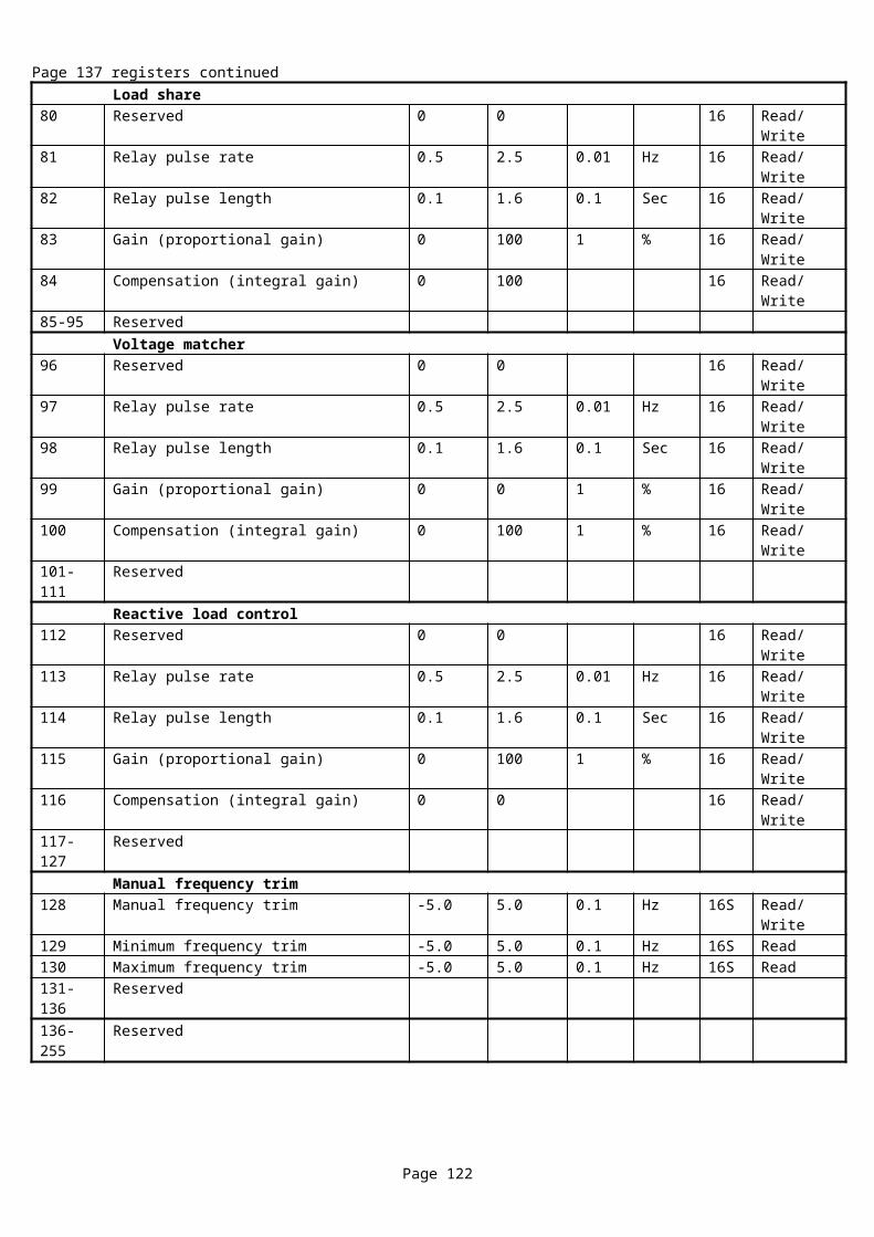
Common register allocation 32-255 Register offset
Name Minimum value
Maximum value
Bits/ sign 8xxx/ 74xx
73xx
335
32 2157 expansion module 0 output A 0 1 16
33 2157 expansion module 0 output B 0 1 16
34 2157 expansion module 0 output C 0 1 16
35 2157 expansion module 0 output D 0 1 16
36 2157 expansion module 0 output E 0 1 16
37 2157 expansion module 0 output F 0 1 16
38 2157 expansion module 0 output G 0 1 16
39 2157 expansion module 0 output H 0 1 16
40-47 2157 expansion module 1 outputs A-H
48-55 2157 expansion module 2 outputs A-H
56-63 2157 expansion module 3 outputs A-H
64-71 2157 expansion module 4 outputs A-H
72-79 2157 expansion module 5 outputs A-H
80-87 2157 expansion module 6 outputs A-H
88-95 2157 expansion module 7 outputs A-H
96-103 2157 expansion module 8 outputs A-H
104-111 2157 expansion module 9 outputs A-H
112 2548 expansion module 0 output A 0 1 16
113 2548 expansion module 0 output B 0 1 16
114 2548 expansion module 0 output C 0 1 16
115 2548 expansion module 0 output D 0 1 16
116 2548 expansion module 0 output E 0 1 16
117 2548 expansion module 0 output F 0 1 16
118 2548 expansion module 0 output G 0 1 16
119 2548 expansion module 0 output H 0 1 16
120 2548 expansion module 0 sounder output 0 1 16
121-129 2548 expansion module 1 outputs A-H & sounder
130-138 2548 expansion module 2 outputs A-H & sounder
139-147 2548 expansion module 3 outputs A-H & sounder
148-156 2548 expansion module 4 outputs A-H & sounder
157-165 2548 expansion module 5 outputs A-H & sounder
166-174 2548 expansion module 6 outputs A-H & sounder
175-183 2548 expansion module 7 outputs A-H & sounder
184-192 2548 expansion module 8 outputs A-H & sounder
193-201 2548 expansion module 9 outputs A-H & sounder
202-255 Reserved
8xxx / 74xx LED allocation by modelRegister Model 8x10/7410 Model 8x60 Model 868014 Stop mode LED Stop mode LED 0xFFFF15 Manual mode LED Manual mode LED 0xFFFF16 0x0000 Test mode LED Manual mode LED17 Auto mode LED Auto mode LED Auto mode LED18 0x0000 Mains available LED Bus 1 live LED19 Bus breaker LED Mains breaker LED Bus breaker LED20 0x0000 Bus breaker LED 0xFFFF21 Gen available LED Bus available LED Bus 2 live LED
Page 122
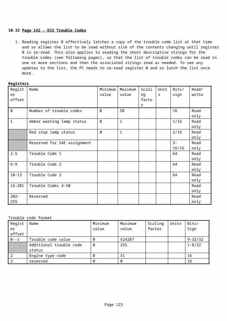
10.49 Page 191 – Virtual output status
1. This page indicates the status of each virtual output.
RegistersRegister offset
Name Minimum value
Maximum value
Scaling factor
Units Bits/ sign Read/write
0 Virtual output 1 status 0 1 16 Read only1 Virtual output 2 status 0 1 16 Read only2 Virtual output 3 status 0 1 16 Read only3 Virtual output 4 status 0 1 16 Read only4 Virtual output 5 status 0 1 16 Read only5 Virtual output 6 status 0 1 16 Read only6 Virtual output 7 status 0 1 16 Read only7 Virtual output 8 status 0 1 16 Read only8 Virtual output 9 status 0 1 16 Read only9 Virtual output 10 status 0 1 16 Read only10 Virtual output 11 status 0 1 16 Read only11 Virtual output 12 status 0 1 16 Read only12 Virtual output 13 status 0 1 16 Read only13 Virtual output 14 status 0 1 16 Read only14 Virtual output 15 status 0 1 16 Read only15 Virtual output 16 status 0 1 16 Read only16 Virtual output 17 status 0 1 16 Read only17 Virtual output 18 status 0 1 16 Read only18 Virtual output 19 status 0 1 16 Read only19 Virtual output 20 status 0 1 16 Read only20-255 Reserved
Page 123
10.50 Page 192 – Configurable output status
1. This page indicates the status of each virtual output.
RegistersRegister offset
Name Minimum value
Maximum value
Scaling factor
Units Bits/ sign Read/write
0 configurable output 1 item A status 0 1 16 Read only1 configurable output 1 item B status 0 1 16 Read only2 configurable output 1 item C status 0 1 16 Read only3 configurable output 2 item A status 0 1 16 Read only4 configurable output 2 item B status 0 1 16 Read only5 configurable output 2 item C status 0 1 16 Read only6 configurable output 3 item A status 0 1 16 Read only7 configurable output 3 item B status 0 1 16 Read only8 configurable output 3 item C status 0 1 16 Read only9-255 Reserved
10.51 Page 193 – Remote control sources
1. This page allows remote control flags to read or written, these can be used to drive outputs, LED’s or the elements of the control logic.
RegistersRegister offset
Name Minimum value
Maximum value
Scaling factor
Units Bits/ sign Read/write
0 Remote control source 1 0 1 16 Read/write1 Remote control source 2 0 1 16 Read/write2 Remote control source 3 0 1 16 Read/write3 Remote control source 4 0 1 16 Read/write4 Remote control source 5 0 1 16 Read/write5 Remote control source 6 0 1 16 Read/write6 Remote control source 7 0 1 16 Read/write7 Remote control source 8 0 1 16 Read/write8 Remote control source 9 0 1 16 Read/write9 Remote control source 10 0 1 16 Read/write10-255 Reserved
Page 124
10.52 Page 200-239 – Unnamed alarm strings
1. This is implemented for 86xx/87xx modules to provide the various unnamed alarm strings (including internal and external digital and analogue inputs).
2. They are used in place of pages 64-95 in the old alarm system, the inactive strings are not implemented to reduce the register count required to support the large number of expansion inputs.
3. The order of the strings is the same as for the input functions and input status pages to simplify the look-up process for the PC software.
4. Reading from the reserved pages will return spaces.5. The register allocation is different for each family.
72xx/73xx family register allocationPage Register offset Name Minimum
valueMaximum value
Bits
200 0 Digital input A active string UNICODE UNICODE 51232 Digital input B active string UNICODE UNICODE 51264 Digital input C active string UNICODE UNICODE 51296 Digital input D active string UNICODE UNICODE 512128 Digital input E active string UNICODE UNICODE 512160 Digital input F active string UNICODE UNICODE 512192 Digital input G active string UNICODE UNICODE 512224 Digital input H active string UNICODE UNICODE 512
201 0 Digital input I active string UNICODE UNICODE 51232 Reserved (for digital input J-P strings)
202 0 2130 expansion module 0 digital input A string UNICODE UNICODE 51232 2130 expansion module 0 digital input B string UNICODE UNICODE 51264 2130 expansion module 0 digital input C string UNICODE UNICODE 51296 2130 expansion module 0 digital input D string UNICODE UNICODE 512128 2130 expansion module 0 digital input E string UNICODE UNICODE 512160 2130 expansion module 0 digital input F string UNICODE UNICODE 512192 2130 expansion module 0 digital input G string UNICODE UNICODE 512224 2130 expansion module 0 digital input H string UNICODE UNICODE 512
203 0-255 2130 expansion module 1 digital input A-H string UNICODE UNICODE 512204 0-255 2130 expansion module 2 digital input A-H string UNICODE UNICODE 512205 0-255 2130 expansion module 3 digital input A-H string UNICODE UNICODE 512206-211 0-255 Reserved for 2130 expansion module 4-9 digital input A-H
stringUNICODE UNICODE 512
212 0 2130 Expansion module 0 input E (low) string UNICODE UNICODE 51232 2130 Expansion module 0 input E (high) string UNICODE UNICODE 51264 2130 Expansion module 0 input F (low) string UNICODE UNICODE 51296 2130 Expansion module 0 input F (high) string UNICODE UNICODE 512128 2130 Expansion module 0 input G (low) string UNICODE UNICODE 512160 2130 Expansion module 0 input G (high) string UNICODE UNICODE 512192 2130 Expansion module 0 input H (low) string UNICODE UNICODE 512224 2130 Expansion module 0 input H (high) string UNICODE UNICODE 512
213 2130 Expansion module 1 inputs E-H strings UNICODE UNICODE 512214 2130 Expansion module 2 inputs E-H strings UNICODE UNICODE 512215 2130 Expansion module 3 inputs E-H strings UNICODE UNICODE 512216-221 Reserved for 2130 Expansion modules 4-9 inputs E-H
stringsUNICODE UNICODE 512
Page 125
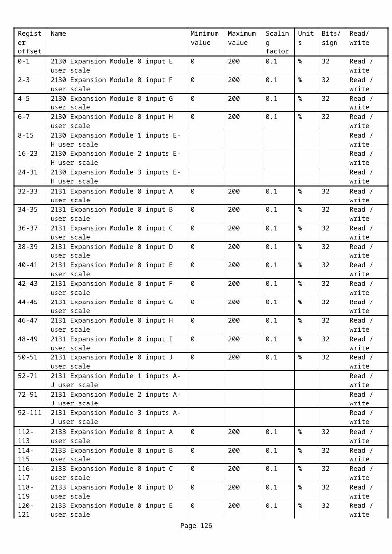
72xx/73xx family register allocation continued222 0 Internal flexible sender input (low) string UNICODE UNICODE 512
32 Internal flexible sender input (high) string UNICODE UNICODE 51264 Maintenance alarm 1 string UNICODE UNICODE 51296 Maintenance alarm 2 string UNICODE UNICODE 512128 Maintenance alarm 3 string UNICODE UNICODE 512160 PLC function 1 string UNICODE UNICODE 512192 PLC function 2 string UNICODE UNICODE 512224 PLC function 3 string UNICODE UNICODE 512
223 0 PLC function 4 string UNICODE UNICODE 51232 PLC function 5 string UNICODE UNICODE 51264 PLC function 6 string UNICODE UNICODE 51296 PLC function 7 string UNICODE UNICODE 512128 PLC function 8 string UNICODE UNICODE 512160 PLC function 9 string UNICODE UNICODE 512192 PLC function 10 string UNICODE UNICODE 512224 PLC function 11 string UNICODE UNICODE 512
224 0 PLC function 12 string UNICODE UNICODE 51232 PLC function 13 string UNICODE UNICODE 51264 PLC function 14 string UNICODE UNICODE 51296 PLC function 15 string UNICODE UNICODE 512128 PLC function 16 string UNICODE UNICODE 512160 PLC function 17 string UNICODE UNICODE 512192 PLC function 18 string UNICODE UNICODE 512224 PLC function 19 string UNICODE UNICODE 512
225 0 PLC function 20 string UNICODE UNICODE 51232 Reserved UNICODE UNICODE 51264 Reserved UNICODE UNICODE 51296 Reserved UNICODE UNICODE 512128 Reserved UNICODE UNICODE 512160 Reserved UNICODE UNICODE 512192 Reserved UNICODE UNICODE 512224 Reserved UNICODE UNICODE 512
226-239 Reserved
Page 126
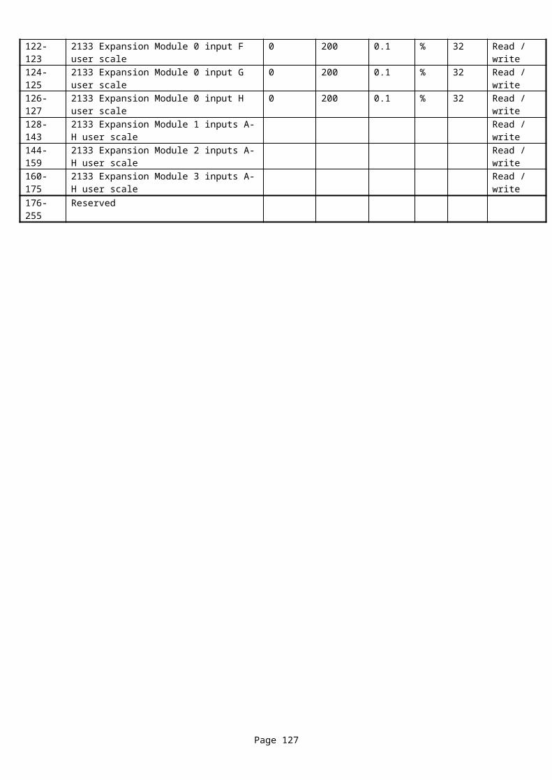
8xxx / 74xx family register allocationPage Register
offsetName Minimum
valueMaximum value
Bits
200 0 Digital input A active string UNICODE UNICODE 51232 Digital input B active string UNICODE UNICODE 51264 Digital input C active string UNICODE UNICODE 51296 Digital input D active string UNICODE UNICODE 512128 Digital input E active string UNICODE UNICODE 512160 Digital input F active string UNICODE UNICODE 512192 Digital input G active string UNICODE UNICODE 512224 Digital input H active string UNICODE UNICODE 512
201 0 Digital input I active string UNICODE UNICODE 51232 Digital input J active string UNICODE UNICODE 51264 Digital input K active string UNICODE UNICODE 51296 Digital input L active string UNICODE UNICODE 512128 Digital input M active string UNICODE UNICODE 512160 Digital input N active string UNICODE UNICODE 512192 Digital input O active string UNICODE UNICODE 512224 Digital input P active string UNICODE UNICODE 512
202 0 Digital input Q active string UNICODE UNICODE 51232 Digital input R active string UNICODE UNICODE 51264 Digital input S active string UNICODE UNICODE 51296 Digital input T active string UNICODE UNICODE 512128 Digital input U active string UNICODE UNICODE 512160 Digital input V active string UNICODE UNICODE 512192 Digital input W active string UNICODE UNICODE 512224 Digital input X active string UNICODE UNICODE 512
203 0 Digital input Y active string UNICODE UNICODE 51232 Digital input Z active string UNICODE UNICODE 51264 Digital input AA active string UNICODE UNICODE 51296 Digital input AB active string UNICODE UNICODE 512128 Digital input AC active string UNICODE UNICODE 512160 Digital input AD active string UNICODE UNICODE 512192 Digital input AE active string UNICODE UNICODE 512224 Digital input AF active string UNICODE UNICODE 512
204 0 2130 expansion module 0 digital input A string UNICODE UNICODE 51232 2130 expansion module 0 digital input B string UNICODE UNICODE 51264 2130 expansion module 0 digital input C string UNICODE UNICODE 51296 2130 expansion module 0 digital input D string UNICODE UNICODE 512128 2130 expansion module 0 digital input E string UNICODE UNICODE 512160 2130 expansion module 0 digital input F string UNICODE UNICODE 512192 2130 expansion module 0 digital input G string UNICODE UNICODE 512224 2130 expansion module 0 digital input H string UNICODE UNICODE 512
205 0-255 2130 expansion module 1 digital input A-H string UNICODE UNICODE 512206 0-255 2130 expansion module 2 digital input A-H string UNICODE UNICODE 512207 0-255 2130 expansion module 3 digital input A-H string UNICODE UNICODE 512208-213 0-255 Reserved for 2130 expansion module 4-9 digital
input A-H stringUNICODE UNICODE 512
214 0 2130 Expansion module 0 input E (low) string UNICODE UNICODE 51232 2130 Expansion module 0 input E (high) string UNICODE UNICODE 51264 2130 Expansion module 0 input F (low) string UNICODE UNICODE 51296 2130 Expansion module 0 input F (high) string UNICODE UNICODE 512128 2130 Expansion module 0 input G (low) string UNICODE UNICODE 512160 2130 Expansion module 0 input G (high) string UNICODE UNICODE 512192 2130 Expansion module 0 input H (low) string UNICODE UNICODE 512224 2130 Expansion module 0 input H (high) string UNICODE UNICODE 512
Page 127
8xxx / 74xx family register allocation215 2130 Expansion module 1 inputs E-H strings UNICODE UNICODE 512216 2130 Expansion module 2 inputs E-H strings UNICODE UNICODE 512217 2130 Expansion module 3 inputs E-H strings UNICODE UNICODE 512218-223 Reserved for 2130 Expansion modules 4-9 inputs E-
H strings224 0 Internal flexible sender 1 input (low) string UNICODE UNICODE 512
32 Internal flexible sender 1 input (high) string UNICODE UNICODE 51264 Internal flexible sender 2 input (low) string UNICODE UNICODE 51296 Internal flexible sender 2 input (high) string UNICODE UNICODE 512128 Internal flexible sender 3 input (low) string UNICODE UNICODE 512160 Internal flexible sender 3 input (high) string UNICODE UNICODE 512192 Internal flexible sender 4 input (low) string UNICODE UNICODE 512224 Internal flexible sender 4 input (high) string UNICODE UNICODE 512
225 0 Internal flexible sender 5 input (low) string UNICODE UNICODE 51232 Internal flexible sender 5 input (high) string UNICODE UNICODE 51264 Maintenance alarm 1 string UNICODE UNICODE 51296 Maintenance alarm 2 string UNICODE UNICODE 512128 Maintenance alarm 3 string UNICODE UNICODE 512160 PLC function 1 string UNICODE UNICODE 512192 PLC function 2 string UNICODE UNICODE 512224 PLC function 3 string UNICODE UNICODE 512
226 0 PLC function 4 string UNICODE UNICODE 51232 PLC function 5 string UNICODE UNICODE 51264 PLC function 6 string UNICODE UNICODE 51296 PLC function 7 string UNICODE UNICODE 512128 PLC function 8 string UNICODE UNICODE 512160 PLC function 9 string UNICODE UNICODE 512192 PLC function 10 string UNICODE UNICODE 512224 PLC function 11 string UNICODE UNICODE 512
227 0 PLC function 12 string UNICODE UNICODE 51232 PLC function 13 string UNICODE UNICODE 51264 PLC function 14 string UNICODE UNICODE 51296 PLC function 15 string UNICODE UNICODE 512128 PLC function 16 string UNICODE UNICODE 512160 PLC function 17 string UNICODE UNICODE 512192 PLC function 18 string UNICODE UNICODE 512224 PLC function 19 string UNICODE UNICODE 512
228 0 PLC function 20 string UNICODE UNICODE 51232 Reserved UNICODE UNICODE 51264 Reserved UNICODE UNICODE 51296 Reserved UNICODE UNICODE 512128 Reserved UNICODE UNICODE 512160 Reserved UNICODE UNICODE 512192 Reserved UNICODE UNICODE 512224 Reserved UNICODE UNICODE 512
229-239 Reserved
Page 128
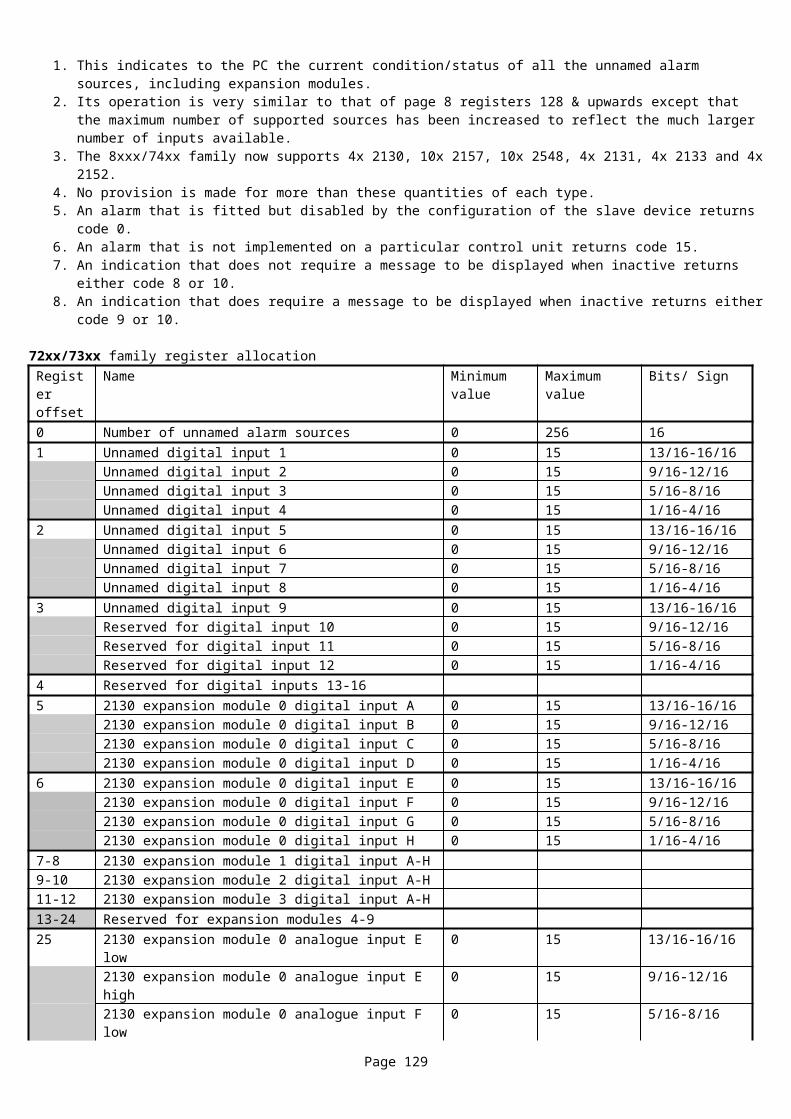
332/333 register allocationPage Register
offsetName Minimum
valueMaximum value
Bits
200 0 Digital input A active string UNICODE UNICODE 51232 Digital input B active string UNICODE UNICODE 51264 Digital input C active string UNICODE UNICODE 51296 Digital input D active string UNICODE UNICODE 512128 Digital input E active string UNICODE UNICODE 512160 Digital input F active string UNICODE UNICODE 512192 Digital input G active string UNICODE UNICODE 512224 Digital input H active string UNICODE UNICODE 512
201 0 Digital input I active string UNICODE UNICODE 51232 Digital input J active string UNICODE UNICODE 51264 Digital input K active string96-255 Reserved for future outputs
202 0 Module description 1 UNICODE UNICODE 51232 Module description 2 UNICODE UNICODE 51264 Site ID UNICODE UNICODE 51296 Generator ID UNICODE UNICODE 512128-255 Reserved for future use
203 0 LCD indicator 1 UNICODE UNICODE 51232 LCD indicator 2 UNICODE UNICODE 51264 LCD indicator 3 UNICODE UNICODE 51296-255 Reserved
204-231 0 Reserved
Page 129
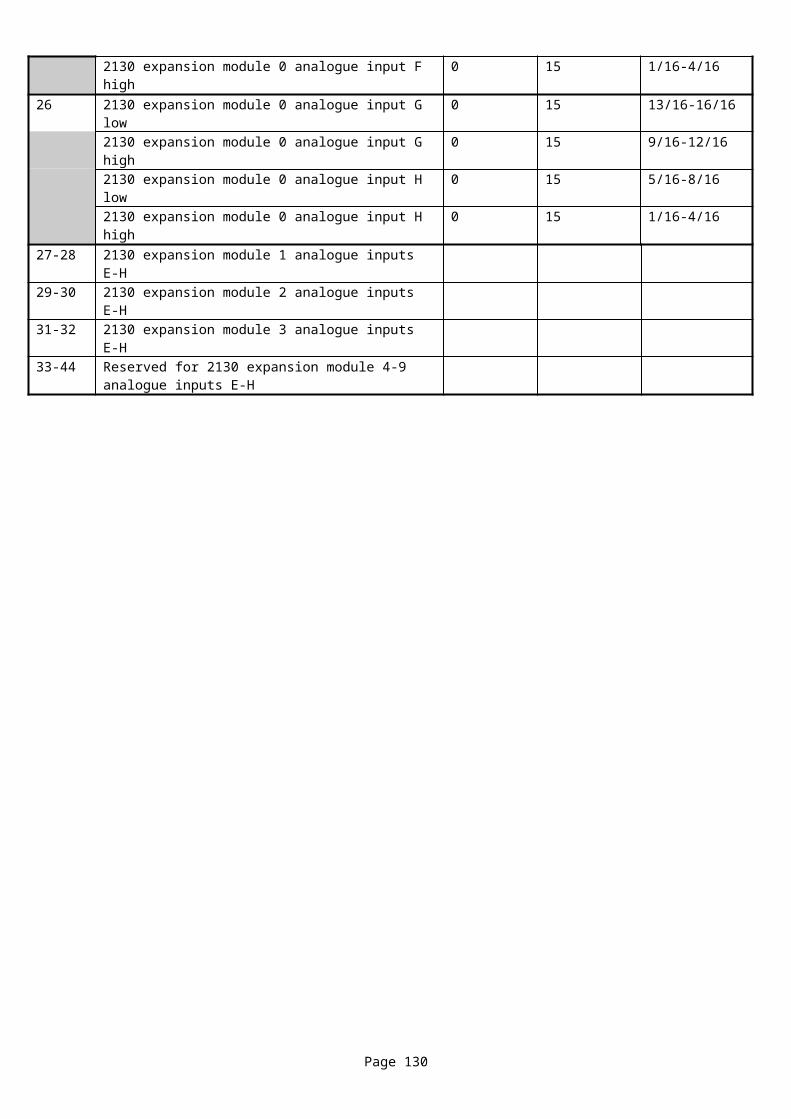
330/331 register allocationPage Register
offsetName Minimum
valueMaximum value
Bits
200 Reserved201 Reserved202 0 Module description 1 UNICODE UNICODE 512
32 Module description 2 UNICODE UNICODE 51264-255 Reserved for future use
203 Reserved204-231 Reserved
334 register allocationPage Register
offsetName Minimum
valueMaximum value
Bits
200 0 Digital input A active string UNICODE UNICODE 51232 Digital input B active string UNICODE UNICODE 51264 Digital input C active string UNICODE UNICODE 51296 Digital input D active string UNICODE UNICODE 512128 Digital input E active string UNICODE UNICODE 512160 Digital input F active string UNICODE UNICODE 512192 Digital input G active string UNICODE UNICODE 512224 Digital input H active string UNICODE UNICODE 512
201 0 Digital input I active string UNICODE UNICODE 51232 Digital input J active string UNICODE UNICODE 51264 Digital input K active string UNICODE UNICODE 51296-255 Reserved for future outputs
202 0 Module description 1 UNICODE UNICODE 51232 Module description 2 UNICODE UNICODE 51264 Site ID (note 1) UNICODE UNICODE 51296 S2 ID (note 1) UNICODE UNICODE 512128-255 Reserved for future use
203 0 LCD indicator / Insert 1 UNICODE UNICODE 51232 LCD indicator / Insert 2 UNICODE UNICODE 51264 LCD indicator / Insert 3 UNICODE UNICODE 51296-255 Reserved
204-231 Reserved
Page 130
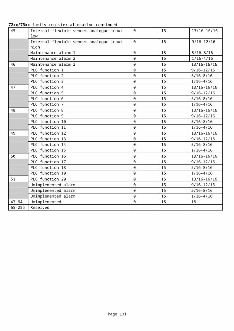
335 register allocationPage Register
offsetName Minimum
valueMaximum value
Bits
200 0 Digital input A active string UNICODE UNICODE 51232 Digital input B active string UNICODE UNICODE 51264 Digital input C active string UNICODE UNICODE 51296 Digital input D active string UNICODE UNICODE 512128 Digital input E active string UNICODE UNICODE 512160 Digital input F active string UNICODE UNICODE 512192 Digital input G active string UNICODE UNICODE 512224 Digital input H active string UNICODE UNICODE 512
201 0 Digital input I active string UNICODE UNICODE 51232 Digital input J active string UNICODE UNICODE 51264 Digital input K active string UNICODE UNICODE 51296 Digital input L active string UNICODE UNICODE 512128-255 Reserved for future outputs
202 0 2130 expansion module 0 digital input A string UNICODE UNICODE 51232 2130 expansion module 0 digital input B string UNICODE UNICODE 51264 2130 expansion module 0 digital input C string UNICODE UNICODE 51296 2130 expansion module 0 digital input D string UNICODE UNICODE 512128 2130 expansion module 0 digital input E string UNICODE UNICODE 512160 2130 expansion module 0 digital input F string UNICODE UNICODE 512192 2130 expansion module 0 digital input G string UNICODE UNICODE 512224 2130 expansion module 0 digital input H string UNICODE UNICODE 512
203 0-255 2130 expansion module 1 digital input A-H string UNICODE UNICODE 512204-211 0-255 Reserved for 2130 expansion module 2-9 digital
input A-H stringUNICODE UNICODE 512
212 0 2130 Expansion module 0 input E (low) string UNICODE UNICODE 51232 2130 Expansion module 0 input E (high) string UNICODE UNICODE 51264 2130 Expansion module 0 input F (low) string UNICODE UNICODE 51296 2130 Expansion module 0 input F (high) string UNICODE UNICODE 512128 2130 Expansion module 0 input G (low) string UNICODE UNICODE 512160 2130 Expansion module 0 input G (high) string UNICODE UNICODE 512192 2130 Expansion module 0 input H (low) string UNICODE UNICODE 512224 2130 Expansion module 0 input H (high) string UNICODE UNICODE 512
213 2130 Expansion module 1 inputs E-H strings UNICODE UNICODE 512214-221 Reserved for 2130 Expansion modules 2-9 inputs
E-H strings
Page 131
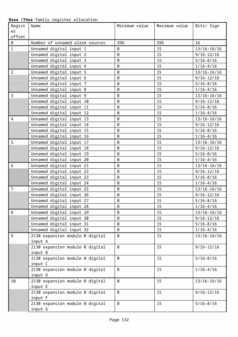
335 register allocation continued222 0 PLC function 1 string UNICODE UNICODE 512
32 PLC function 2 string UNICODE UNICODE 51264 PLC function 3 string UNICODE UNICODE 51296 PLC function 4 string UNICODE UNICODE 512128 PLC function 5 string UNICODE UNICODE 512160 PLC function 6 string UNICODE UNICODE 512192 PLC function 7 string UNICODE UNICODE 512224 PLC function 8 string UNICODE UNICODE 512
223 0 PLC function 9 string UNICODE UNICODE 51232 PLC function 10 string UNICODE UNICODE 51264 PLC function 11 string UNICODE UNICODE 51296 PLC function 12 string UNICODE UNICODE 512128 PLC function 13 string UNICODE UNICODE 512160 PLC function 14 string UNICODE UNICODE 512192 PLC function 15 string UNICODE UNICODE 512224 PLC function 16 string UNICODE UNICODE 512
224 0 PLC function 17 string UNICODE UNICODE 51232 PLC function 18 string UNICODE UNICODE 51264 PLC function 19 string UNICODE UNICODE 51296 PLC function 20 string UNICODE UNICODE 512128-255 Reserved
225 0 Module description 1 UNICODE UNICODE 51232 Module description 2 UNICODE UNICODE 51264 Site ID (note 1) UNICODE UNICODE 51296 S2 ID (note 1) UNICODE UNICODE 512128-255 Reserved for future use
226-239 0 Reserved
Page 132
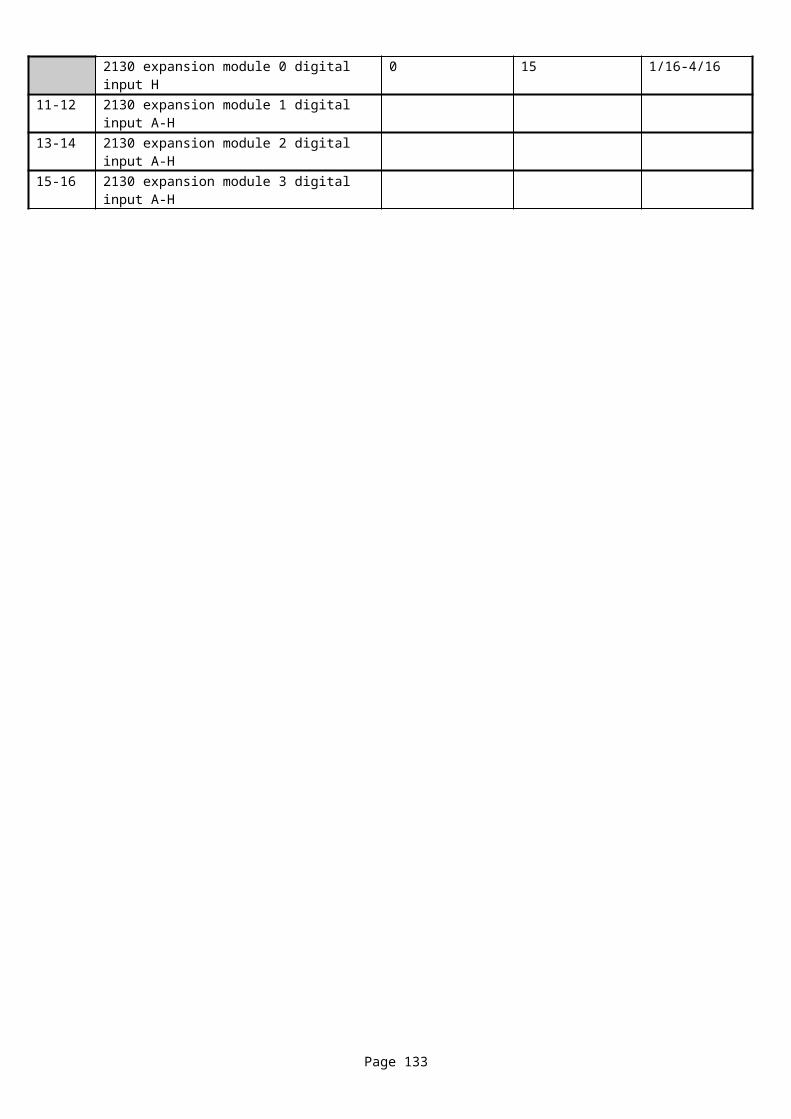
10.53 Page 240-246 – Analogue Input Name Strings
1. This page provides the name strings for user configurable analogue inputs.2. The order of the strings is the same as for the input functions and input status pages to simplify the look-up process for the PC
software.3. The register allocation is different for each family.
72xx/73xx family register allocationPage Register
offsetName Minimum
valueMaximum value
Bits
240 0 2130 Expansion module 0 input E name string UNICODE UNICODE 51232 2130 Expansion module 0 input F name string UNICODE UNICODE 51264 2130 Expansion module 0 input G name string UNICODE UNICODE 51296 2130 Expansion module 0 input H name string UNICODE UNICODE 512128 2130 Expansion module 1 input E name string UNICODE UNICODE 512160 2130 Expansion module 1 input F name string UNICODE UNICODE 512192 2130 Expansion module 1 input G name string UNICODE UNICODE 512224 2130 Expansion module 1 input H name string UNICODE UNICODE 512
241 0 2130 Expansion module 2 input E name string UNICODE UNICODE 51232 2130 Expansion module 2 input F name string UNICODE UNICODE 51264 2130 Expansion module 2 input G name string UNICODE UNICODE 51296 2130 Expansion module 2 input H name string UNICODE UNICODE 512128 2130 Expansion module 3 input E name string UNICODE UNICODE 512160 2130 Expansion module 3 input F name string UNICODE UNICODE 512192 2130 Expansion module 3 input G name string UNICODE UNICODE 512224 2130 Expansion module 3 input H name string UNICODE UNICODE 512
242-244 Reserved for 2130 expansion module 4-9 input E-H name strings
245 0 Internal Flexible sender name string UNICODE UNICODE 51232 Reserved64 Reserved96 Reserved128 Reserved160 Reserved192 Reserved224 Reserved
246 0 Reserved32 Reserved64 Reserved96 Reserved128 Reserved160 Reserved192 Reserved224 Reserved
Page 133

8xxx/74xx family register allocationPage Register
offsetName Minimum
valueMaximum value
Bits
240 0 2130 Expansion module 0 input E name string UNICODE UNICODE 51232 2130 Expansion module 0 input F name string UNICODE UNICODE 51264 2130 Expansion module 0 input G name string UNICODE UNICODE 51296 2130 Expansion module 0 input H name string UNICODE UNICODE 512128 2130 Expansion module 1 input E name string UNICODE UNICODE 512160 2130 Expansion module 1 input F name string UNICODE UNICODE 512192 2130 Expansion module 1 input G name string UNICODE UNICODE 512224 2130 Expansion module 1 input H name string UNICODE UNICODE 512
241 0 2130 Expansion module 2 input E name string UNICODE UNICODE 51232 2130 Expansion module 2 input F name string UNICODE UNICODE 51264 2130 Expansion module 2 input G name string UNICODE UNICODE 51296 2130 Expansion module 2 input H name string UNICODE UNICODE 512128 2130 Expansion module 3 input E name string UNICODE UNICODE 512160 2130 Expansion module 3 input F name string UNICODE UNICODE 512192 2130 Expansion module 3 input G name string UNICODE UNICODE 512224 2130 Expansion module 3 input H name string UNICODE UNICODE 512
242-244 Reserved245 0 Internal Flexible sender 1 name string UNICODE UNICODE 512
32 Internal Flexible sender 2 name string UNICODE UNICODE 51264 Internal Flexible sender 3 name string UNICODE UNICODE 51296 Internal Flexible sender 4 name string UNICODE UNICODE 512128 Internal Flexible sender 5 name string UNICODE UNICODE 512160 Configurable output 1 string UNICODE UNICODE 512192 Configurable output 2 string UNICODE UNICODE 512224 Configurable output 3 string UNICODE UNICODE 512
246 0 Reserved32 Reserved64 Reserved96 Reserved128 Reserved160 Reserved192 Reserved224 Reserved
335 register allocationPage Register
offsetName Minimum
valueMaximum value
Bits
240 0 2130 Expansion module 0 input E name string UNICODE UNICODE 51232 2130 Expansion module 0 input F name string UNICODE UNICODE 51264 2130 Expansion module 0 input G name string UNICODE UNICODE 51296 2130 Expansion module 0 input H name string UNICODE UNICODE 512128 2130 Expansion module 1 input E name string UNICODE UNICODE 512160 2130 Expansion module 1 input F name string UNICODE UNICODE 512192 2130 Expansion module 1 input G name string UNICODE UNICODE 512224 2130 Expansion module 1 input H name string UNICODE UNICODE 512
241-244 Reserved for 2130 Expansion modules 2-9 inputs E-H strings
245-246 Reserved
Page 134
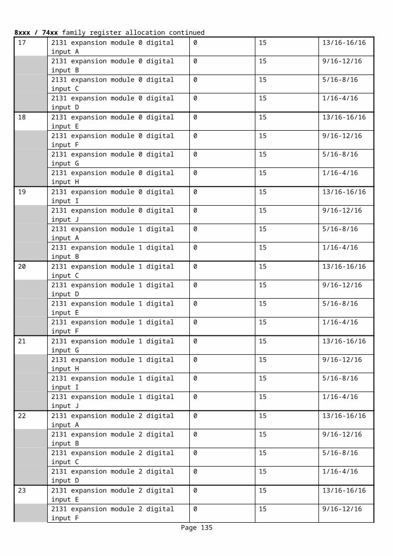
10.54 Page 250 – Misc strings
1. This page provides the strings for the insert card.
RegistersPage Register
offsetName Minimum
valueMaximum value
Bits
250 0 LED Insert card string 1 UNICODE UNICODE 51232 LED Insert card string 2 UNICODE UNICODE 51264 LED Insert card string 3 UNICODE UNICODE 51296 LED Insert card string 4 UNICODE UNICODE 512128 Reserved UNICODE UNICODE 512160 Reserved UNICODE UNICODE 512192 Reserved UNICODE UNICODE 512224 Reserved UNICODE UNICODE 512
Page 135
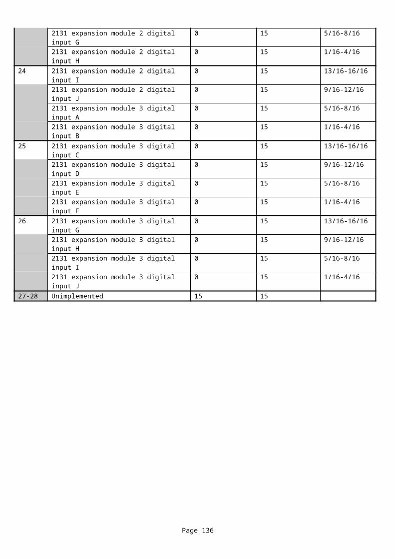
_________________________________________________________________________________________________________
Page 136