Embed Size (px)
Citation preview
Software revision: 5.2x
GE Digital Energy part number: 1601-0152-AB
GE publication code: GEK-106491K
GE Digital Energy
650 Markland Street
Markham, Ontario
Canada L6C 0M1
Tel: +1 905 927 7070 Fax: +1 905 927 5098
Internet: http://www.gedigitalenergy.comGE Digital Energy's Quality
Management System is registered to ISO9001:2008
QMI # 005094*1601-0152-AB*
GE Digital Energy
469 Motor Management Relay
Communications Guide
© 2013 GE Multilin Incorporated. All rights reserved.
GE Digital Energy — 750/760 Feeder Management Relay instruction manual for revision5.2x
750/760 Feeder Management Relay, is a registered trademark of GE Multilin Inc.
The contents of this manual are the property of GE Multilin Inc. This documentation isfurnished on license and may not be reproduced in whole or in part without the permissionof GE Multilin Inc. The content of this manual is for informational use only and is subject tochange without notice.
Part numbers contained in this manual are subject to change without notice, and shouldtherefore be verified by GE Multilin Inc. before ordering.
Part number: 1601-0152-AB (January 2013)
CHAPTER TOC:
469 MOTOR MANAGEMENT RELAY – COMMUNICATIONS GUIDE TOC-2
Table of Contents
MODBUS PROTOCOL Electrical Interface ...........................................................................................................................................1Modbus RTU Protocol .....................................................................................................................................1Data Frame Format and Data Rate.........................................................................................................2Data Packet Format ........................................................................................................................................2CRC-16 Algorithm.............................................................................................................................................3Timing ....................................................................................................................................................................4
MODBUS FUNCTIONS Supported Functions ......................................................................................................................................5Read Relay Coil / Digital Input Status .....................................................................................................5Read Setpoints and Actual Values ...........................................................................................................7Execute Operation ...........................................................................................................................................8Store Single Setpoint.......................................................................................................................................8Read Device Status..........................................................................................................................................9Loopback Test................................................................................................................................................. 10Store Multiple Setpoints.............................................................................................................................. 10Performing Commands .............................................................................................................................. 11Error Responses ............................................................................................................................................. 12
MODBUS MEMORY MAP
Memory Map Information ......................................................................................................................... 13User-Definable Memory Map Area ....................................................................................................... 13Event Recorder ...............................................................................................................................................15Waveform Capture....................................................................................................................................... 15469 Memory Map .......................................................................................................................................... 19Format Codes............................................................................................................................................... 109
DEVICENET PROTOCOL
Overview......................................................................................................................................................... 124Poll Data.......................................................................................................................................................... 124Change of State (COS) .............................................................................................................................. 124DeviceNet Objects...................................................................................................................................... 125469 Specific Objects.................................................................................................................................. 131DeviceNet Data Formats ........................................................................................................................ 140

TOC-2 469 MOTOR MANAGEMENT RELAY – COMMUNICATIONS GUIDE
CHAPTER TOC:
469 MOTOR MANAGEMENT RELAY – COMMUNICATIONS GUIDE 1
469 Motor Management Relay
Communications Guide
GE Digital Energy
Communications Guide
Modbus Protocol
Electrical Interface
The hardware or electrical interface is one of the following: one of two 2-wire RS485 ports from the rear terminal connector or the RS232 from the front panel connector. In a 2-wire RS485 link, data flow is bidirectional. Data flow is half duplex for both the RS485 and the RS232 ports. That is, data is never transmitted and received at the same time. RS485 lines should be connected in a daisy chain configuration (avoid star connections) with a terminating network installed at each end of the link, i.e. at the master end and at the slave farthest from the master. The terminating network should consist of a 120 Ω resistor in series with a 1 nF ceramic capacitor when used with Belden 9841 RS485 wire. The value of the terminating resistors should be equal to the characteristic impedance of the line. This is approximately 120 Ω for standard #22 AWG twisted pair wire. Shielded wire should always be used to minimize noise. Polarity is important in RS485 communications. Each ‘+’ terminal of every 469 must be connected together for the system to operate. See Chapter 2 of the 469 manual for details on correct serial port wiring.
Modbus RTU Protocol
The 469 implements a subset of the AEG Modicon Modbus RTU serial communication standard. Many popular programmable controllers support this protocol directly with a suitable interface card allowing direct connection of relays. Although the Modbus protocol is hardware independent, the 469 interfaces include two 2-wire RS485 ports and one RS232 port. Modbus is a single master, multiple slave protocol suitable for a multi-drop configuration as provided by RS485 hardware. In this configuration up to 32 slaves can be daisy-chained together on a single communication channel.
The 469 is always a slave. It cannot be programmed as a master. Computers or PLCs are commonly programmed as masters. The Modbus protocol exists in two versions: Remote Terminal Unit (RTU, binary) and ASCII. Only the RTU version is supported by the 469. Monitoring, programming and control functions are possible using read and write register commands.
2 469 MOTOR MANAGEMENT RELAY – COMMUNICATIONS GUIDE
COMMUNICATIONS GUIDE
Data Frame Format and Data Rate
One data frame of an asynchronous transmission to or from an 469 is default to 1 start bit, 8 data bits, and 1 stop bit . This produces a 10 bit data frame. This is important for transmission through modems at high bit rates (11-bit data frames are not supported by Hayes modems at bit rates of greater than 300 bps). The parity bit is optional as odd or even. If it is programmed as odd or even, the data frame consists of 1 start bit, 8 data bits, 1 parity bit, and 1 stop bit.
Modbus protocol can be implemented at any standard communication speed. The 469 RS485/RS232 ports support operation at 1200, 2400, 4800, 9600, and 19200 baud.
Data Packet Format
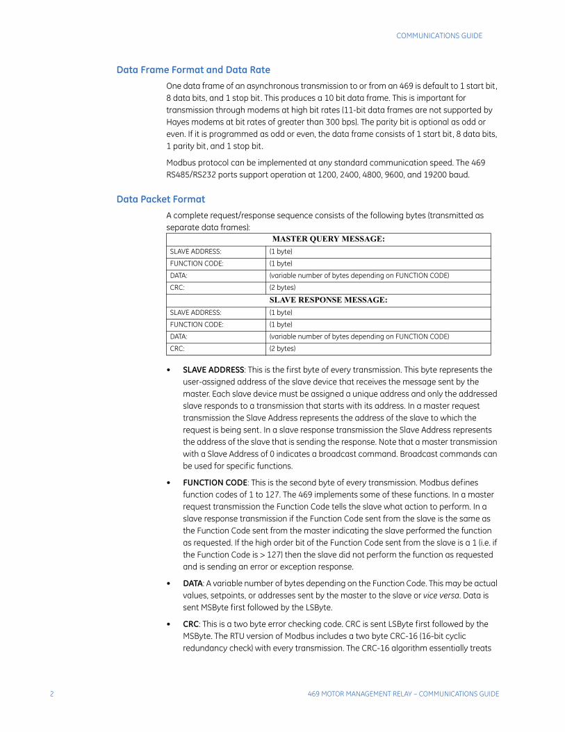
A complete request/response sequence consists of the following bytes (transmitted as separate data frames):
• SLAVE ADDRESS: This is the first byte of every transmission. This byte represents the user-assigned address of the slave device that receives the message sent by the master. Each slave device must be assigned a unique address and only the addressed slave responds to a transmission that starts with its address. In a master request transmission the Slave Address represents the address of the slave to which the request is being sent. In a slave response transmission the Slave Address represents the address of the slave that is sending the response. Note that a master transmission with a Slave Address of 0 indicates a broadcast command. Broadcast commands can be used for specific functions.
• FUNCTION CODE: This is the second byte of every transmission. Modbus defines function codes of 1 to 127. The 469 implements some of these functions. In a master request transmission the Function Code tells the slave what action to perform. In a slave response transmission if the Function Code sent from the slave is the same as the Function Code sent from the master indicating the slave performed the function as requested. If the high order bit of the Function Code sent from the slave is a 1 (i.e. if the Function Code is > 127) then the slave did not perform the function as requested and is sending an error or exception response.
• DATA: A variable number of bytes depending on the Function Code. This may be actual values, setpoints, or addresses sent by the master to the slave or vice versa. Data is sent MSByte first followed by the LSByte.
• CRC: This is a two byte error checking code. CRC is sent LSByte first followed by the MSByte. The RTU version of Modbus includes a two byte CRC-16 (16-bit cyclic redundancy check) with every transmission. The CRC-16 algorithm essentially treats
MASTER QUERY MESSAGE:
SLAVE ADDRESS: (1 byte)
FUNCTION CODE: (1 byte)
DATA: (variable number of bytes depending on FUNCTION CODE)
CRC: (2 bytes)
SLAVE RESPONSE MESSAGE:
SLAVE ADDRESS: (1 byte)
FUNCTION CODE: (1 byte)
DATA: (variable number of bytes depending on FUNCTION CODE)
CRC: (2 bytes)
COMMUNICATIONS GUIDE
469 MOTOR MANAGEMENT RELAY – COMMUNICATIONS GUIDE 3
the entire data stream (data bits only; start, stop and parity ignored) as one continuous binary number. This number is first shifted left 16 bits and then divided by a characteristic polynomial (11000000000000101B). The 16-bit remainder of the division is appended to the end of the transmission, LSByte first. The resulting message including CRC, when divided by the same polynomial at the receiver will give a zero remainder if no transmission errors have occurred.
If an 469 Modbus slave device receives a transmission in which an error is indicated by the CRC-16 calculation, the slave device will not respond to the transmission. A CRC-16 error indicates than one or more bytes of the transmission were received incorrectly and thus the entire transmission should be ignored in order to avoid the 469 performing any incorrect operation. The CRC-16 calculation is an industry standard method used for error detection. An algorithm is included here to assist programmers in situations where no standard CRC-16 calculation routines are available.
CRC-16 Algorithm
Once the following algorithm is complete, the working register “A” will contain the CRC value to be transmitted. Note that this algorithm requires the characteristic polynomial to be reverse bit ordered. The MSbit of the characteristic polynomial is dropped since it does not affect the value of the remainder.
The symbols used in the algorithm are shown below:
--> data transfer
A; Alow; Ahigh 16-bit working register; low and high order bytes of A (the 16-bit working register)
CRC 16 bit CRC-16 result
i, j loop counters
(+) logical EXCLUSIVE-OR operator
N total number of data bytes
Di i-th data byte (i = 0 to N – 1)
G 16 bit characteristic polynomial = 1010000000000001 (binary) with MSbit dropped and bit order reversed
shr (x) right shift operator (the LSbit of x is shifted into a carry flag, a '0' is shifted into the MSbit of x, all other bits are shifted right one location)
The CRC algorithm is shown below:
1. FFFF (hex) --> A
2. 0 --> i
3. 0 --> j
4. Di (+) Alow --> Alow5. j + 1 --> j
6. shr (A)
7. Is there a carry?No: go to step 8.
Yes: G (+) A --> A and continue.
8. Is j = 8? No: go to 5.
Yes: continue.
4 469 MOTOR MANAGEMENT RELAY – COMMUNICATIONS GUIDE
COMMUNICATIONS GUIDE
9. i + 1 --> i
10.Is i = N? No: go to 3.
Yes: continue.
11.A --> CRC
Timing
Data packet synchronization is maintained by timing constraints. The receiving device must measure the time between the reception of characters. If three and one half character times elapse without a new character or completion of the packet, then the communication link must be reset (i.e. all slaves start listening for a new transmission from the master). Thus at 9600 baud a delay of greater than 3.5 × 1 / 9600 × 10 = 3.65 ms will cause the communication link to be reset.
COMMUNICATIONS GUIDE
469 MOTOR MANAGEMENT RELAY – COMMUNICATIONS GUIDE 5
Modbus Functions
Supported Functions
The following functions are supported by the 469:
Modbus Function Code 01: Read Relay CoilModbus Function Code 02: Read Digital Input StatusModbus Function Code 03: Read Setpoints and Actual ValuesModbus Function Code 04: Read Setpoints and Actual ValuesModbus Function Code 05: Execute OperationModbus Function Code 06: Store Single SetpointModbus Function Code 07: Read Device StatusModbus Function Code 08: Loopback TestModbus Function Code 16: Store Multiple Setpoints
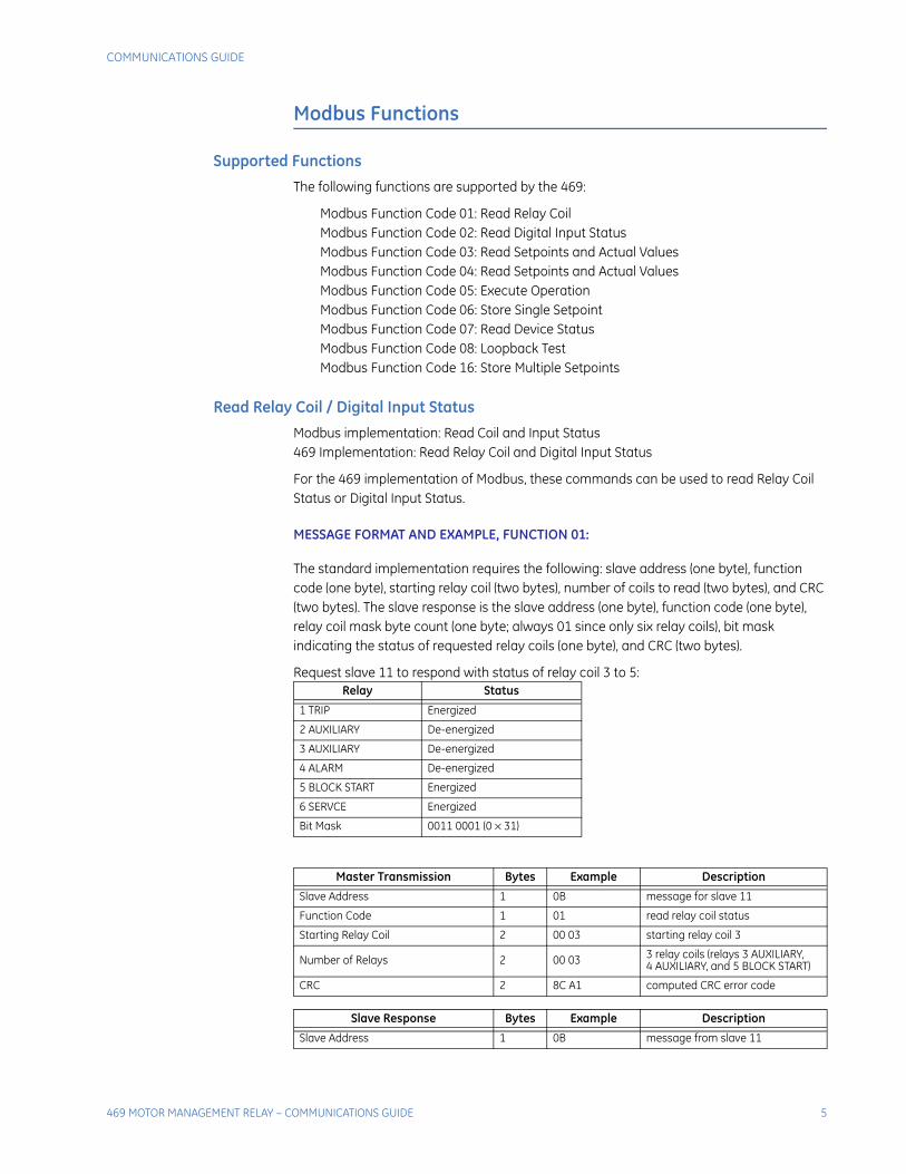
Read Relay Coil / Digital Input Status
Modbus implementation: Read Coil and Input Status469 Implementation: Read Relay Coil and Digital Input Status
For the 469 implementation of Modbus, these commands can be used to read Relay Coil Status or Digital Input Status.
MESSAGE FORMAT AND EXAMPLE, FUNCTION 01:
The standard implementation requires the following: slave address (one byte), function code (one byte), starting relay coil (two bytes), number of coils to read (two bytes), and CRC (two bytes). The slave response is the slave address (one byte), function code (one byte), relay coil mask byte count (one byte; always 01 since only six relay coils), bit mask indicating the status of requested relay coils (one byte), and CRC (two bytes).
Request slave 11 to respond with status of relay coil 3 to 5:Relay Status
1 TRIP Energized
2 AUXILIARY De-energized
3 AUXILIARY De-energized
4 ALARM De-energized
5 BLOCK START Energized
6 SERVCE Energized
Bit Mask 0011 0001 (0 × 31)
Master Transmission Bytes Example Description
Slave Address 1 0B message for slave 11
Function Code 1 01 read relay coil status
Starting Relay Coil 2 00 03 starting relay coil 3
Number of Relays 2 00 03 3 relay coils (relays 3 AUXILIARY, 4 AUXILIARY, and 5 BLOCK START)
CRC 2 8C A1 computed CRC error code
Slave Response Bytes Example Description
Slave Address 1 0B message from slave 11
6 469 MOTOR MANAGEMENT RELAY – COMMUNICATIONS GUIDE
COMMUNICATIONS GUIDE
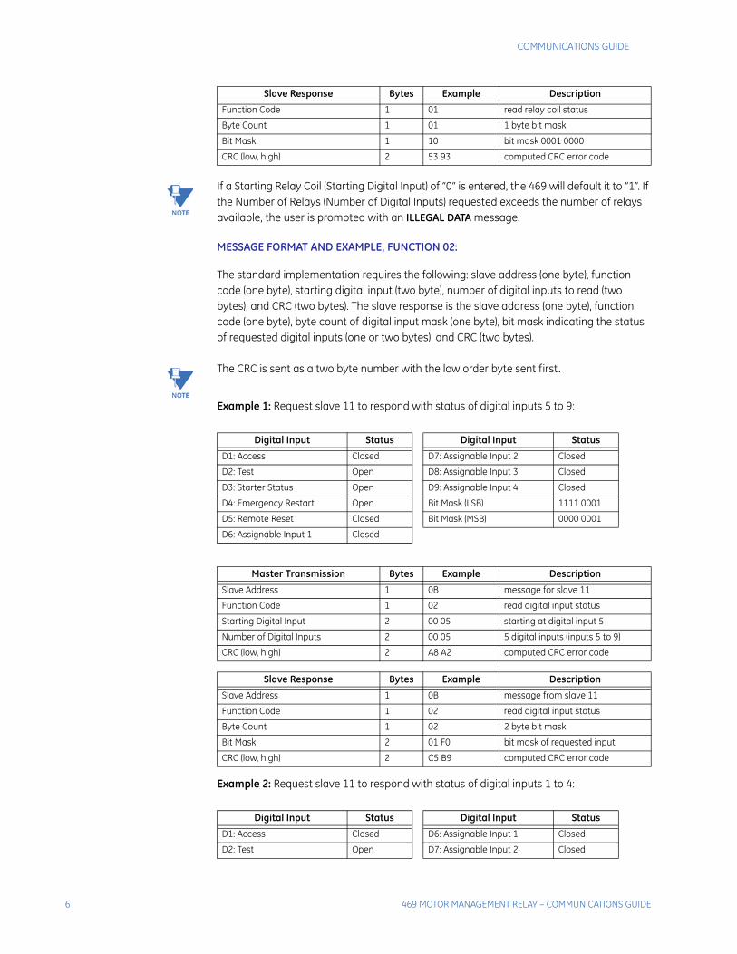
Note If a Starting Relay Coil (Starting Digital Input) of “0” is entered, the 469 will default it to “1”. If the Number of Relays (Number of Digital Inputs) requested exceeds the number of relays available, the user is prompted with an ILLEGAL DATA message.
MESSAGE FORMAT AND EXAMPLE, FUNCTION 02:
The standard implementation requires the following: slave address (one byte), function code (one byte), starting digital input (two byte), number of digital inputs to read (two bytes), and CRC (two bytes). The slave response is the slave address (one byte), function code (one byte), byte count of digital input mask (one byte), bit mask indicating the status of requested digital inputs (one or two bytes), and CRC (two bytes).
Note The CRC is sent as a two byte number with the low order byte sent first.
Example 1: Request slave 11 to respond with status of digital inputs 5 to 9:
Example 2: Request slave 11 to respond with status of digital inputs 1 to 4:
Function Code 1 01 read relay coil status
Byte Count 1 01 1 byte bit mask
Bit Mask 1 10 bit mask 0001 0000
CRC (low, high) 2 53 93 computed CRC error code
Slave Response Bytes Example Description
Digital Input Status Digital Input Status
D1: Access Closed D7: Assignable Input 2 Closed
D2: Test Open D8: Assignable Input 3 Closed
D3: Starter Status Open D9: Assignable Input 4 Closed
D4: Emergency Restart Open Bit Mask (LSB) 1111 0001
D5: Remote Reset Closed Bit Mask (MSB) 0000 0001
D6: Assignable Input 1 Closed
Master Transmission Bytes Example Description
Slave Address 1 0B message for slave 11
Function Code 1 02 read digital input status
Starting Digital Input 2 00 05 starting at digital input 5
Number of Digital Inputs 2 00 05 5 digital inputs (inputs 5 to 9)
CRC (low, high) 2 A8 A2 computed CRC error code
Slave Response Bytes Example Description
Slave Address 1 0B message from slave 11
Function Code 1 02 read digital input status
Byte Count 1 02 2 byte bit mask
Bit Mask 2 01 F0 bit mask of requested input
CRC (low, high) 2 C5 B9 computed CRC error code
Digital Input Status Digital Input Status
D1: Access Closed D6: Assignable Input 1 Closed
D2: Test Open D7: Assignable Input 2 Closed
COMMUNICATIONS GUIDE
469 MOTOR MANAGEMENT RELAY – COMMUNICATIONS GUIDE 7
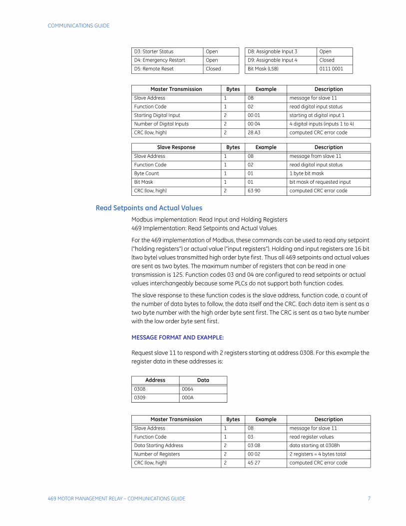
Read Setpoints and Actual Values
Modbus implementation: Read Input and Holding Registers469 Implementation: Read Setpoints and Actual Values
For the 469 implementation of Modbus, these commands can be used to read any setpoint (“holding registers”) or actual value (“input registers”). Holding and input registers are 16 bit (two byte) values transmitted high order byte first. Thus all 469 setpoints and actual values are sent as two bytes. The maximum number of registers that can be read in one transmission is 125. Function codes 03 and 04 are configured to read setpoints or actual values interchangeably because some PLCs do not support both function codes.
The slave response to these function codes is the slave address, function code, a count of the number of data bytes to follow, the data itself and the CRC. Each data item is sent as a two byte number with the high order byte sent first. The CRC is sent as a two byte number with the low order byte sent first.
MESSAGE FORMAT AND EXAMPLE:
Request slave 11 to respond with 2 registers starting at address 0308. For this example the register data in these addresses is:
D3: Starter Status Open D8: Assignable Input 3 Open
D4: Emergency Restart Open D9: Assignable Input 4 Closed
D5: Remote Reset Closed Bit Mask (LSB) 0111 0001
Master Transmission Bytes Example Description
Slave Address 1 0B message for slave 11
Function Code 1 02 read digital input status
Starting Digital Input 2 00 01 starting at digital input 1
Number of Digital Inputs 2 00 04 4 digital inputs (inputs 1 to 4)
CRC (low, high) 2 28 A3 computed CRC error code
Slave Response Bytes Example Description
Slave Address 1 0B message from slave 11
Function Code 1 02 read digital input status
Byte Count 1 01 1 byte bit mask
Bit Mask 1 01 bit mask of requested input
CRC (low, high) 2 63 90 computed CRC error code
Address Data
0308 0064
0309 000A
Master Transmission Bytes Example Description
Slave Address 1 0B message for slave 11
Function Code 1 03 read register values
Data Starting Address 2 03 08 data starting at 0308h
Number of Registers 2 00 02 2 registers = 4 bytes total
CRC (low, high) 2 45 27 computed CRC error code
8 469 MOTOR MANAGEMENT RELAY – COMMUNICATIONS GUIDE
COMMUNICATIONS GUIDE
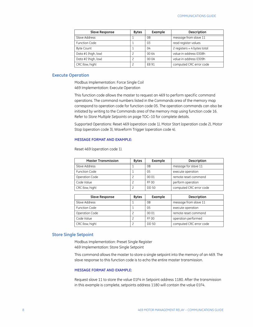
Execute Operation
Modbus Implementation: Force Single Coil469 Implementation: Execute Operation
This function code allows the master to request an 469 to perform specific command operations. The command numbers listed in the Commands area of the memory map correspond to operation code for function code 05. The operation commands can also be initiated by writing to the Commands area of the memory map using function code 16. Refer to Store Multiple Setpoints on page TOC–10 for complete details.
Supported Operations: Reset 469 (operation code 1), Motor Start (operation code 2), Motor Stop (operation code 3), Waveform Trigger (operation code 4).
MESSAGE FORMAT AND EXAMPLE:
Reset 469 (operation code 1).
Store Single Setpoint
Modbus Implementation: Preset Single Register469 Implementation: Store Single Setpoint
This command allows the master to store a single setpoint into the memory of an 469. The slave response to this function code is to echo the entire master transmission.
MESSAGE FORMAT AND EXAMPLE:
Request slave 11 to store the value 01F4 in Setpoint address 1180. After the transmission in this example is complete, setpoints address 1180 will contain the value 01F4.
Slave Response Bytes Example Description
Slave Address 1 0B message from slave 11
Function Code 1 03 read register values
Byte Count 1 04 2 registers = 4 bytes total
Data #1 (high, low) 2 00 64 value in address 0308h
Data #2 (high, low) 2 00 0A value in address 0309h
CRC (low, high) 2 EB 91 computed CRC error code
Master Transmission Bytes Example Description
Slave Address 1 0B message for slave 11
Function Code 1 05 execute operation
Operation Code 2 00 01 remote reset command
Code Value 2 FF 00 perform operation
CRC (low, high) 2 DD 50 computed CRC error code
Slave Response Bytes Example Description
Slave Address 1 0B message from slave 11
Function Code 1 05 execute operation
Operation Code 2 00 01 remote reset command
Code Value 2 FF 00 operation performed
CRC (low, high) 2 DD 50 computed CRC error code
COMMUNICATIONS GUIDE
469 MOTOR MANAGEMENT RELAY – COMMUNICATIONS GUIDE 9
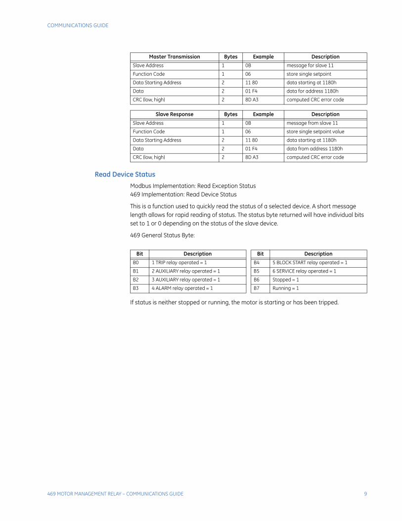
Read Device Status
Modbus Implementation: Read Exception Status469 Implementation: Read Device Status
This is a function used to quickly read the status of a selected device. A short message length allows for rapid reading of status. The status byte returned will have individual bits set to 1 or 0 depending on the status of the slave device.
469 General Status Byte:
If status is neither stopped or running, the motor is starting or has been tripped.
Master Transmission Bytes Example Description
Slave Address 1 0B message for slave 11
Function Code 1 06 store single setpoint
Data Starting Address 2 11 80 data starting at 1180h
Data 2 01 F4 data for address 1180h
CRC (low, high) 2 8D A3 computed CRC error code
Slave Response Bytes Example Description
Slave Address 1 0B message from slave 11
Function Code 1 06 store single setpoint value
Data Starting Address 2 11 80 data starting at 1180h
Data 2 01 F4 data from address 1180h
CRC (low, high) 2 8D A3 computed CRC error code
Bit Description Bit Description
B0 1 TRIP relay operated = 1 B4 5 BLOCK START relay operated = 1
B1 2 AUXILIARY relay operated = 1 B5 6 SERVICE relay operated = 1
B2 3 AUXILIARY relay operated = 1 B6 Stopped = 1
B3 4 ALARM relay operated = 1 B7 Running = 1
10 469 MOTOR MANAGEMENT RELAY – COMMUNICATIONS GUIDE
COMMUNICATIONS GUIDE
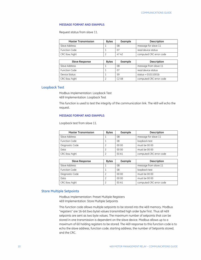
MESSAGE FORMAT AND EXAMPLE:
Request status from slave 11.
Loopback Test
Modbus Implementation: Loopback Test469 Implementation: Loopback Test
This function is used to test the integrity of the communication link. The 469 will echo the request.
MESSAGE FORMAT AND EXAMPLE:
Loopback test from slave 11.
Store Multiple Setpoints
Modbus Implementation: Preset Multiple Registers469 Implementation: Store Multiple Setpoints
This function code allows multiple setpoints to be stored into the 469 memory. Modbus “registers” are 16-bit (two byte) values transmitted high order byte first. Thus all 469 setpoints are sent as two byte values. The maximum number of setpoints that can be stored in one transmission is dependent on the slave device. Modbus allows up to a maximum of 60 holding registers to be stored. The 469 response to this function code is to echo the slave address, function code, starting address, the number of Setpoints stored, and the CRC.
Master Transmission Bytes Example Description
Slave Address 1 0B message for slave 11
Function Code 1 07 read device status
CRC (low, high) 2 47 42 computed CRC error code
Slave Response Bytes Example Description
Slave Address 1 0B message from slave 11
Function Code 1 07 read device status
Device Status 1 59 status = 01011001b
CRC (low, high) 2 C2 08 computed CRC error code
Master Transmission Bytes Example Description
Slave Address 1 0B message for slave 11
Function Code 1 08 loopback test
Diagnostic Code 2 00 00 must be 00 00
Data 2 00 00 must be 00 00
CRC (low, high) 2 E0 A1 computed CRC error code
Slave Response Bytes Example Description
Slave Address 1 0B message from slave 11
Function Code 1 08 loopback test
Diagnostic Code 2 00 00 must be 00 00
Data 2 00 00 must be 00 00
CRC (low, high) 2 E0 A1 computed CRC error code
COMMUNICATIONS GUIDE
469 MOTOR MANAGEMENT RELAY – COMMUNICATIONS GUIDE 11
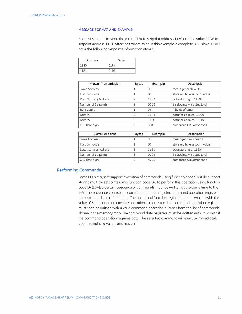
MESSAGE FORMAT AND EXAMPLE:
Request slave 11 to store the value 01F4 to setpoint address 1180 and the value 01DE to setpoint address 1181. After the transmission in this example is complete, 469 slave 11 will have the following Setpoints information stored:
Performing Commands
Some PLCs may not support execution of commands using function code 5 but do support storing multiple setpoints using function code 16. To perform this operation using function code 16 (10H), a certain sequence of commands must be written at the same time to the 469. The sequence consists of: command function register, command operation register and command data (if required). The command function register must be written with the value of 5 indicating an execute operation is requested. The command operation register must then be written with a valid command operation number from the list of commands shown in the memory map. The command data registers must be written with valid data if the command operation requires data. The selected command will execute immediately upon receipt of a valid transmission.
Address Data
1180 01F4
1181 01DE
Master Transmission Bytes Example Description
Slave Address 1 0B message for slave 11
Function Code 1 10 store multiple setpoint value
Data Starting Address 2 11 80 data starting at 1180h
Number of Setpoints 2 00 02 2 setpoints = 4 bytes total
Byte Count 1 04 4 bytes of data
Data #1 2 01 F4 data for address 1180h
Data #2 2 01 DE data for address 1181h
CRC (low, high) 2 DB B1 computed CRC error code
Slave Response Bytes Example Description
Slave Address 1 0B message from slave 11
Function Code 1 10 store multiple setpoint value
Data Starting Address 2 11 80 data starting at 1180h
Number of Setpoints 2 00 02 2 setpoints = 4 bytes total
CRC (low, high) 2 45 B6 computed CRC error code
12 469 MOTOR MANAGEMENT RELAY – COMMUNICATIONS GUIDE
COMMUNICATIONS GUIDE
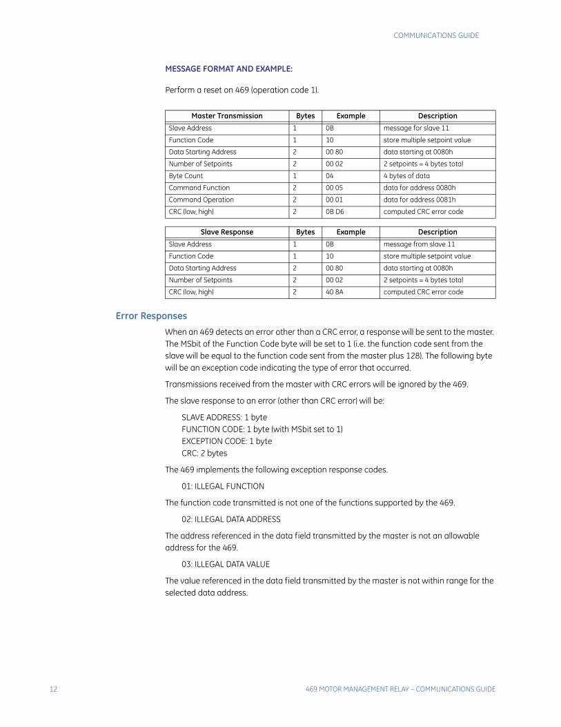
MESSAGE FORMAT AND EXAMPLE:
Perform a reset on 469 (operation code 1).
Error Responses
When an 469 detects an error other than a CRC error, a response will be sent to the master. The MSbit of the Function Code byte will be set to 1 (i.e. the function code sent from the slave will be equal to the function code sent from the master plus 128). The following byte will be an exception code indicating the type of error that occurred.
Transmissions received from the master with CRC errors will be ignored by the 469.
The slave response to an error (other than CRC error) will be:
SLAVE ADDRESS: 1 byteFUNCTION CODE: 1 byte (with MSbit set to 1)EXCEPTION CODE: 1 byteCRC: 2 bytes
The 469 implements the following exception response codes.
01: ILLEGAL FUNCTION
The function code transmitted is not one of the functions supported by the 469.
02: ILLEGAL DATA ADDRESS
The address referenced in the data field transmitted by the master is not an allowable address for the 469.
03: ILLEGAL DATA VALUE
The value referenced in the data field transmitted by the master is not within range for the selected data address.
Master Transmission Bytes Example Description
Slave Address 1 0B message for slave 11
Function Code 1 10 store multiple setpoint value
Data Starting Address 2 00 80 data starting at 0080h
Number of Setpoints 2 00 02 2 setpoints = 4 bytes total
Byte Count 1 04 4 bytes of data
Command Function 2 00 05 data for address 0080h
Command Operation 2 00 01 data for address 0081h
CRC (low, high) 2 0B D6 computed CRC error code
Slave Response Bytes Example Description
Slave Address 1 0B message from slave 11
Function Code 1 10 store multiple setpoint value
Data Starting Address 2 00 80 data starting at 0080h
Number of Setpoints 2 00 02 2 setpoints = 4 bytes total
CRC (low, high) 2 40 8A computed CRC error code
COMMUNICATIONS GUIDE
469 MOTOR MANAGEMENT RELAY – COMMUNICATIONS GUIDE 13
Modbus Memory Map
Memory Map Information
The data stored in the 469 is grouped as setpoints and actual values. Setpoints can be read and written by a master computer. Actual Values are read only. All Setpoints and actual values are stored as two-byte values. That is, each register address is the address of a two-byte value. Addresses are listed in hexadecimal. Data values (setpoint ranges, increments, factory values) are in decimal.
Note Many Modbus communications drivers add 40001d to the actual address of the register addresses. For example: if address 0h was to be read, 40001d would be the address required by the Modbus communications driver; if address 320h (800d) was to be read, 40801d would be the address required by the Modbus communications driver.
User-Definable Memory Map Area
The 469 has a powerful feature, called the User Definable Memory Map, which allows a computer to read up to 125 non-consecutive data registers (setpoints or actual values) by using one Modbus packet. It is often necessary for a master computer to continuously poll various values in each of the connected slave relays. If these values are scattered throughout the memory map, reading them would require numerous transmissions and would burden the communication link. The User Definable Memory Map can be programmed to join any memory map address to one in the block of consecutive User Map locations, so that they can be accessed by reading these consecutive locations.
The User Definable area has two sections:
1. User-Definable Addresses 1 to 125 (memory map registers 0180h to 01FCh) that contain 125 actual values or setpoints register addresses.
2. User-Definable Values 1 to 125 (memory map registers 0100h to 017Ch) that contains the data in the corresponding user-definable addresses.
Register data that is separated in the rest of the memory map may be remapped to adjacent register addresses in the values area. This is accomplished by writing to register addresses in the user-definable address area. This improves data throughput and can eliminate the need for multiple read command sequences.
For example, if the values of Average Phase Current (register address 0306h) and Hottest Stator RTD Temperature (register address 0320h) are required to be read from an 469, their addresses may be remapped as follows:
1. Write 0306h to address 0180h (User Definable Address #1) using function code 06 or 16.
2. Write 0307h to address 0181h (User Definable Address #2) using function code 06 or 16 (Average Phase Current is a double register number).
3. Write 0320h to address 0182h (User Definable Address #3) using function code 06 or 16.
A read (function code 03 or 04) of registers 0100h (User Definable Address #1) and 0101h (User Definable Address #2) will return the Phase A Current and register 0102h (User Definable Address #3) will return Hottest Stator RTD Temperature.
14 469 MOTOR MANAGEMENT RELAY – COMMUNICATIONS GUIDE
COMMUNICATIONS GUIDE
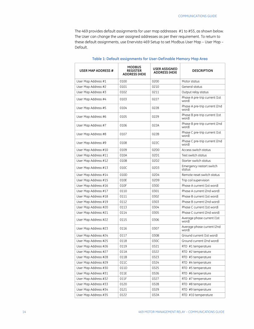
The 469 provides default assignments for user map addresses #1 to #55, as shown below. The User can change the user assigned addresses as per their requirement. To return to these default assignments, use Enervista 469 Setup to set Modbus User Map – User Map – Default.
Table 1: Default assignments for User-Definable Memory Map Area
USER MAP ADDRESS #MODBUS REGISTER
ADDRESS (HEX)
USER ASSIGNED ADDRESS (HEX) DESCRIPTION
User Map Address #1 0100 0200 Motor status
User Map Address #2 0101 0210 General status
User Map Address #3 0102 0211 Output relay status
User Map Address #4 0103 0227 Phase A pre-trip current (1st word)
User Map Address #5 0104 0228 Phase A pre-trip current (2nd word)
User Map Address #6 0105 0229 Phase B pre-trip current (1st word)
User Map Address #7 0106 022A Phase B pre-trip current (2nd word)
User Map Address #8 0107 022B Phase C pre-trip current (1st word)
User Map Address #9 0108 022C Phase C pre-trip current (2nd word)
User Map Address #10 0109 02D0 Access switch status
User Map Address #11 010A 02D1 Test switch status
User Map Address #12 010B 02D2 Starter switch status
User Map Address #13 010C 02D3 Emergency restart switch status
User Map Address #14 010D 02D4 Remote reset switch status
User Map Address #15 010E 02D9 Trip coil supervision
User Map Address #16 010F 0300 Phase A current (1st word)
User Map Address #17 0110 0301 Phase A current (2nd word)
User Map Address #18 0111 0302 Phase B current (1st word)
User Map Address #19 0112 0303 Phase B current (2nd word)
User Map Address #20 0113 0304 Phase C current (1st word)
User Map Address #21 0114 0305 Phase C current (2nd word)
User Map Address #22 0115 0306 Average phase current (1st word)
User Map Address #23 0116 0307 Average phase current (2nd word)
User Map Address #24 0117 030B Ground current (1st word)
User Map Address #25 0118 030C Ground current (2nd word)
User Map Address #26 0119 0321 RTD #1 temperature
User Map Address #27 011A 0322 RTD #2 temperature
User Map Address #28 011B 0323 RTD #3 temperature
User Map Address #29 011C 0324 RTD #4 temperature
User Map Address #30 011D 0325 RTD #5 temperature
User Map Address #31 011E 0326 RTD #6 temperature
User Map Address #32 011F 0327 RTD #7 temperature
User Map Address #33 0120 0328 RTD #8 temperature
User Map Address #34 0121 0329 RTD #9 temperature
User Map Address #35 0122 032A RTD #10 temperature
COMMUNICATIONS GUIDE
469 MOTOR MANAGEMENT RELAY – COMMUNICATIONS GUIDE 15
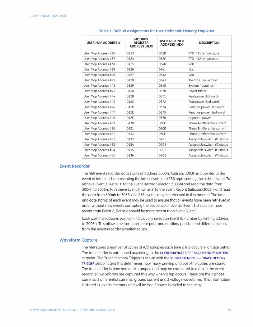
Event Recorder
The 469 event recorder data starts at address 3000h. Address 3003h is a pointer to the event of interest (1 representing the latest event and 256 representing the oldest event). To retrieve Event 1, write ‘1’ to the Event Record Selector (3003h) and read the data from 3004h to 3035h. To retrieve Event 2, write ‘2’ to the Event Record Selector (3003h) and read the data from 3004h to 3035h. All 256 events may be retrieved in this manner. The time and date stamp of each event may be used to ensure that all events have been retrieved in order without new events corrupting the sequence of events (Event 1 should be more recent than Event 2, Event 2 should be more recent than Event 3, etc.).
Each communications port can individually select an Event ID number by writing address to 3003h. This allows the front port, rear port, and auxiliary port to read different events from the event recorder simultaneously.
Waveform Capture
The 469 stores a number of cycles of A/D samples each time a trip occurs in a trace buffer. The trace buffer is partitioned according to the S1 PREFERENCES TRACE MEMORY BUFFERS setpoint. The Trace Memory Trigger is set up with the S1 PREFERENCES TRACE MEMORY
TRIGGER setpoint and this determines how many pre-trip and post-trip cycles are stored. The trace buffer is time and date stamped and may be correlated to a trip in the event record. 10 waveforms are captured this way when a trip occurs. These are the 3 phase currents, 3 differential currents, ground current and 3 voltage waveforms. This information is stored in volatile memory and will be lost if power is cycled to the relay.
User Map Address #36 0123 032B RTD #11 temperature
User Map Address #37 0124 032C RTD #12 temperature
User Map Address #38 0125 0340 Vab
User Map Address #39 0126 0341 Vbc
User Map Address #40 0127 0342 Vca
User Map Address #41 0128 0343 Average line voltage
User Map Address #42 0129 0348 System frequency
User Map Address #43 012A 0370 Power factor
User Map Address #44 012B 0371 Real power (1st word)
User Map Address #45 012C 0372 Real power (2nd word)
User Map Address #46 012D 0374 Reactive power (1st word)
User Map Address #47 012E 0375 Reactive power (2nd word)
User Map Address #48 012F 0376 Apparent power
User Map Address #49 0130 030D Phase A differential current
User Map Address #50 0131 030E Phase B differential current
User Map Address #51 0132 030F Phase C differential current
User Map Address #52 0133 02D5 Assignable switch #1 status
User Map Address #53 0134 02D6 Assignable switch #2 status
User Map Address #54 0135 02D7 Assignable switch #3 status
User Map Address #55 0136 02D8 Assignable switch #4 status
Table 1: Default assignments for User-Definable Memory Map Area
USER MAP ADDRESS #MODBUS REGISTER
ADDRESS (HEX)
USER ASSIGNED ADDRESS (HEX) DESCRIPTION
16 469 MOTOR MANAGEMENT RELAY – COMMUNICATIONS GUIDE
COMMUNICATIONS GUIDE
To access the captured waveforms, select the waveform of interest by writing its trace memory channel (see following table) to the Trace Memory Channel Selector (address 30F1h). Then read the trace memory data from address 3100h to 3700h. There are 720 samples per second when the nominal system frequency (modbus address 11C0) has been set to 60 Hz or set to Variable. There are 600 samples per second when the nominal system frequency has been set to 50 Hz. Sample rate may vary within 5% when 469 is tracking the frequency of the input voltage. The actual sample rate for a trace is 12 x Trace Memory Sampling Frequency, modbus address 30F9. The values read are in actual amperes or volts.
Address 30F8h shows the number of traces taken. To access the latest use the value at address 30F0h. To access more than 1 trace, reduce this value to access the older traces.
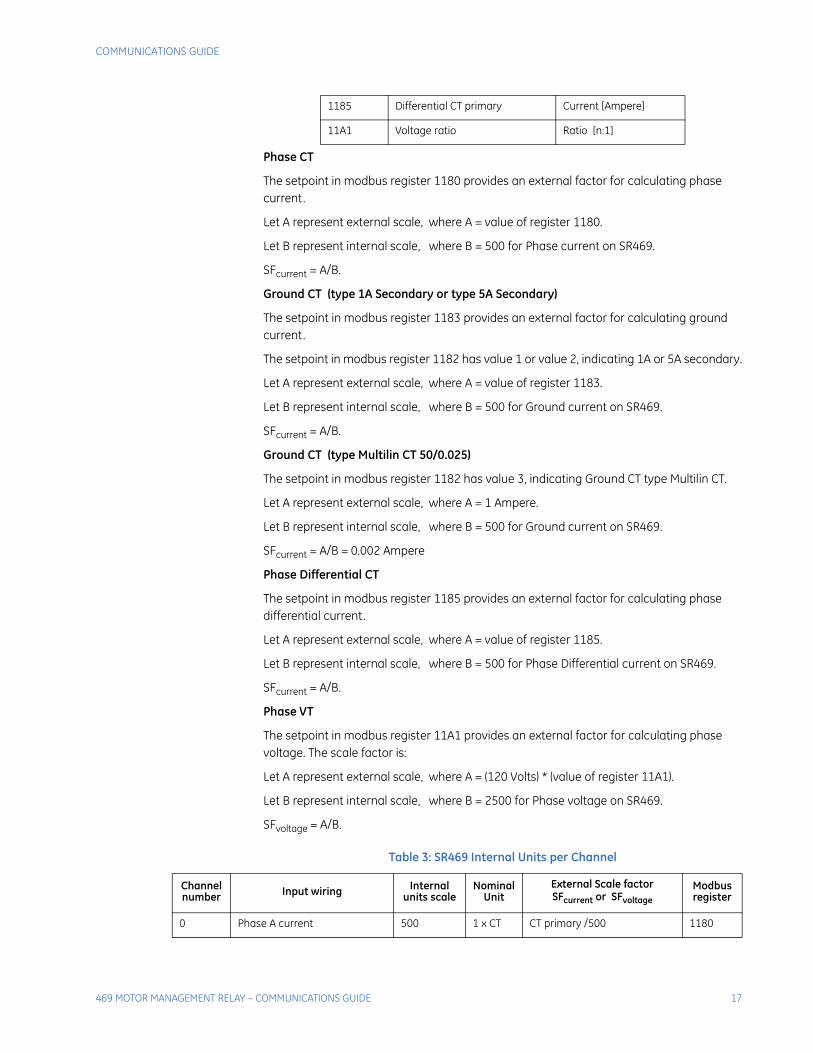
INTERNAL UNITS SCALE
SR 469 presents modbus values for trace data in internal units. The scale of internal units for currents is 1 x CT = 500. The scale of internal units for voltage is 1 x VT = 2500.
Let SFcurrent represent scale factor for phase current or ground current.
Let SFvoltage represent scale factor for phase voltage.
SFcurrent = (CT primary )/ (500 )
SFvoltage= (120 V )* (VT ratio) / (2500 )
To calculate a value in units of Ampere from a waveform trace sample for Current:
Phase current [ Ampere ] = (trace sample value) * SFcurrent
To calculate a value in units of Volt from a waveform trace sample for Voltage:
Phase voltage [ Volt ] = (trace sample value) * SFvoltage
Table 2: Modbus registers related to trace value scale factor
TRACE MEMORY CHANNEL WAVEFORM
0 Phase A current
1 Phase B current
2 Phase C current
3 Differential phase A current
4 Differential phase B current
5 Differential phase C current
6 Ground current
7 Phase A voltage
8 Phase B voltage
9 Phase C voltage
10 Relay output states
Setpoint Description Units of measure
1180 CT primary Current [Ampere]
1182 Ground CT Type Current [Ampere]
1183 Ground CT primary Current [Ampere]
COMMUNICATIONS GUIDE
469 MOTOR MANAGEMENT RELAY – COMMUNICATIONS GUIDE 17
Phase CT
The setpoint in modbus register 1180 provides an external factor for calculating phase current.
Let A represent external scale, where A = value of register 1180.
Let B represent internal scale, where B = 500 for Phase current on SR469.
SFcurrent = A/B.
Ground CT (type 1A Secondary or type 5A Secondary)
The setpoint in modbus register 1183 provides an external factor for calculating ground current.
The setpoint in modbus register 1182 has value 1 or value 2, indicating 1A or 5A secondary.
Let A represent external scale, where A = value of register 1183.
Let B represent internal scale, where B = 500 for Ground current on SR469.
SFcurrent = A/B.
Ground CT (type Multilin CT 50/0.025)
The setpoint in modbus register 1182 has value 3, indicating Ground CT type Multilin CT.
Let A represent external scale, where A = 1 Ampere.
Let B represent internal scale, where B = 500 for Ground current on SR469.
SFcurrent = A/B = 0.002 Ampere
Phase Differential CT
The setpoint in modbus register 1185 provides an external factor for calculating phase differential current.
Let A represent external scale, where A = value of register 1185.
Let B represent internal scale, where B = 500 for Phase Differential current on SR469.
SFcurrent = A/B.
Phase VT
The setpoint in modbus register 11A1 provides an external factor for calculating phase voltage. The scale factor is:
Let A represent external scale, where A = (120 Volts) * (value of register 11A1).
Let B represent internal scale, where B = 2500 for Phase voltage on SR469.
SFvoltage = A/B.
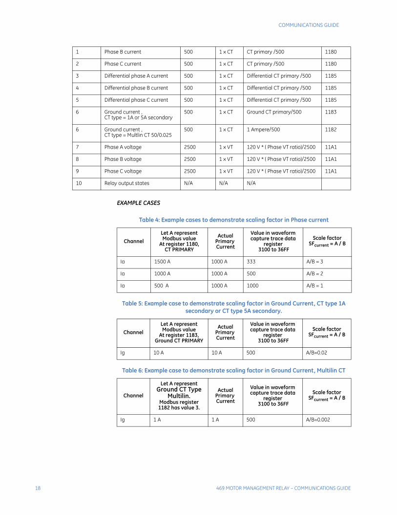
Table 3: SR469 Internal Units per Channel
1185 Differential CT primary Current [Ampere]
11A1 Voltage ratio Ratio [n:1]
Channelnumber Input wiring Internal
units scaleNominal
UnitExternal Scale factorSFcurrent or SFvoltage
Modbus register
0 Phase A current 500 1 x CT CT primary /500 1180
18 469 MOTOR MANAGEMENT RELAY – COMMUNICATIONS GUIDE
COMMUNICATIONS GUIDE
EXAMPLE CASES
Table 4: Example cases to demonstrate scaling factor in Phase current
Table 5: Example case to demonstrate scaling factor in Ground Current, CT type 1A secondary or CT type 5A secondary.
Table 6: Example case to demonstrate scaling factor in Ground Current, Multilin CT
1 Phase B current 500 1 x CT CT primary /500 1180
2 Phase C current 500 1 x CT CT primary /500 1180
3 Differential phase A current 500 1 x CT Differential CT primary /500 1185
4 Differential phase B current 500 1 x CT Differential CT primary /500 1185
5 Differential phase C current 500 1 x CT Differential CT primary /500 1185
6 Ground current , CT type = 1A or 5A secondary
500 1 x CT Ground CT primary/500 1183
6 Ground current , CT type = Multlin CT 50/0.025
500 1 x CT 1 Ampere/500 1182
7 Phase A voltage 2500 1 x VT 120 V * ( Phase VT ratio)/2500 11A1
8 Phase B voltage 2500 1 x VT 120 V * ( Phase VT ratio)/2500 11A1
9 Phase C voltage 2500 1 x VT 120 V * ( Phase VT ratio)/2500 11A1
10 Relay output states N/A N/A N/A
Channel
Let A representModbus value
At register 1180,CT PRIMARY
ActualPrimary Current
Value in waveform capture trace data
register 3100 to 36FF
Scale factorSFcurrent = A / B
Ia 1500 A 1000 A 333 A/B = 3
Ia 1000 A 1000 A 500 A/B = 2
Ia 500 A 1000 A 1000 A/B = 1
Channel
Let A representModbus value
At register 1183,Ground CT PRIMARY
ActualPrimary Current
Value in waveform capture trace data
register 3100 to 36FF
Scale factorSFcurrent = A / B
Ig 10 A 10 A 500 A/B=0.02
Channel
Let A representGround CT Type
Multilin.Modbus register 1182 has value 3.
ActualPrimary Current
Value in waveform capture trace data
register 3100 to 36FF
Scale factorSFcurrent = A / B
Ig 1 A 1 A 500 A/B=0.002
COMMUNICATIONS GUIDE
469 MOTOR MANAGEMENT RELAY – COMMUNICATIONS GUIDE 19
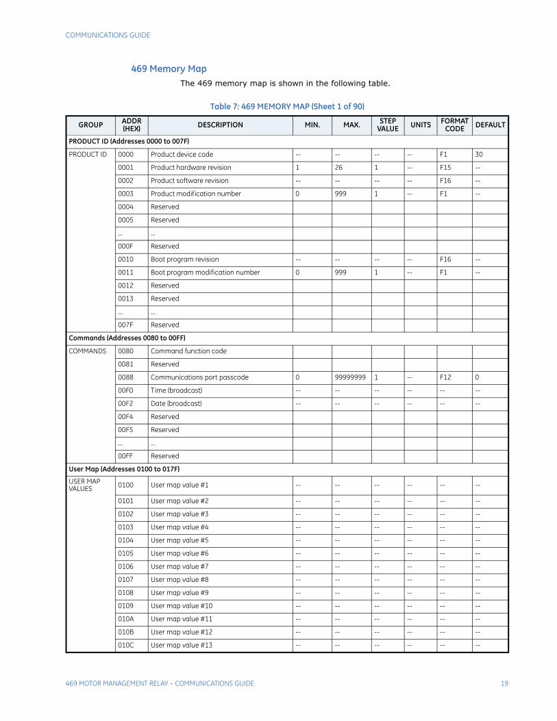
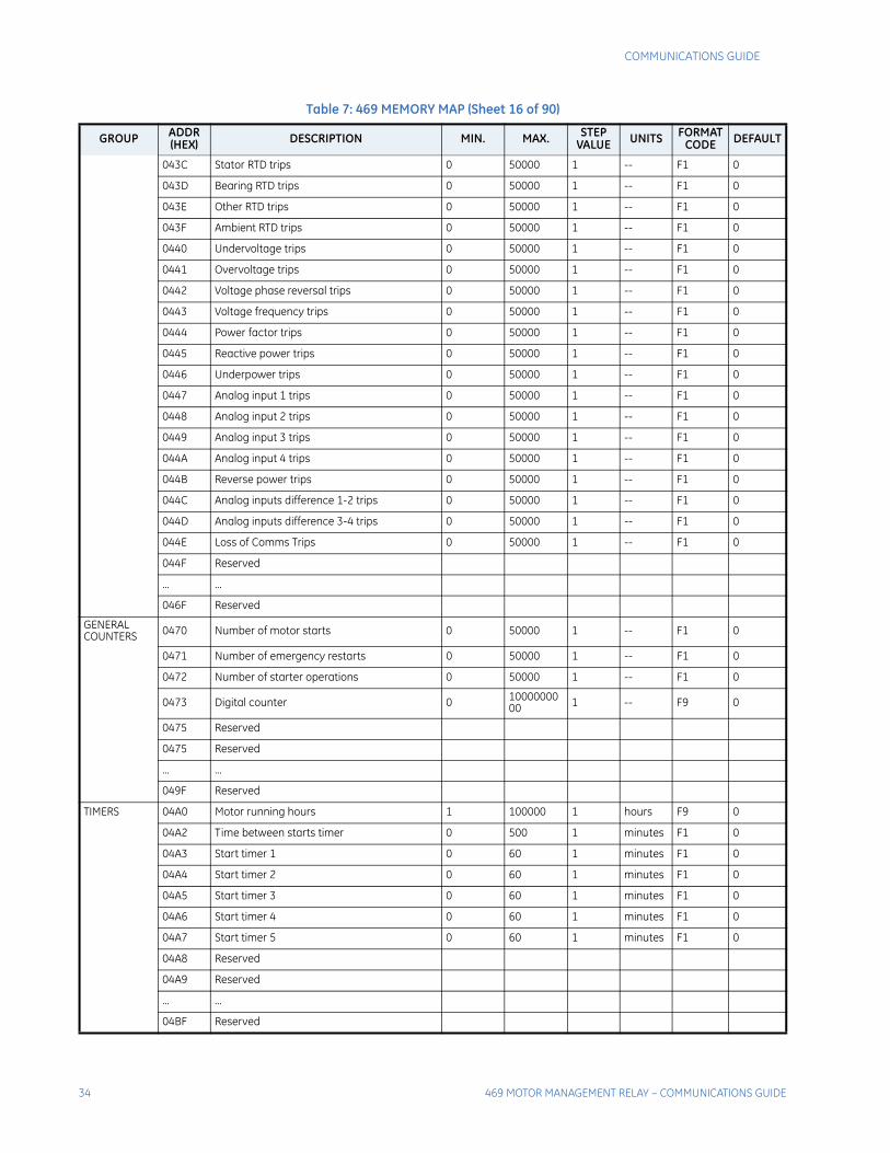
469 Memory MapThe 469 memory map is shown in the following table.
Table 7: 469 MEMORY MAP (Sheet 1 of 90)
GROUP ADDR(HEX) DESCRIPTION MIN. MAX. STEP
VALUE UNITS FORMATCODE DEFAULT
PRODUCT ID (Addresses 0000 to 007F)
PRODUCT ID 0000 Product device code -- -- -- -- F1 30
0001 Product hardware revision 1 26 1 -- F15 --
0002 Product software revision -- -- -- -- F16 --
0003 Product modification number 0 999 1 -- F1 --
0004 Reserved
0005 Reserved
... ...
000F Reserved
0010 Boot program revision -- -- -- -- F16 --
0011 Boot program modification number 0 999 1 -- F1 --
0012 Reserved
0013 Reserved
... ...
007F Reserved
Commands (Addresses 0080 to 00FF)
COMMANDS 0080 Command function code
0081 Reserved
0088 Communications port passcode 0 99999999 1 -- F12 0
00F0 Time (broadcast) -- -- -- -- -- --
00F2 Date (broadcast) -- -- -- -- -- --
00F4 Reserved
00F5 Reserved
... ...
00FF Reserved
User Map (Addresses 0100 to 017F)
USER MAP VALUES 0100 User map value #1 -- -- -- -- -- --
0101 User map value #2 -- -- -- -- -- --
0102 User map value #3 -- -- -- -- -- --
0103 User map value #4 -- -- -- -- -- --
0104 User map value #5 -- -- -- -- -- --
0105 User map value #6 -- -- -- -- -- --
0106 User map value #7 -- -- -- -- -- --
0107 User map value #8 -- -- -- -- -- --
0108 User map value #9 -- -- -- -- -- --
0109 User map value #10 -- -- -- -- -- --
010A User map value #11 -- -- -- -- -- --
010B User map value #12 -- -- -- -- -- --
010C User map value #13 -- -- -- -- -- --

20 469 MOTOR MANAGEMENT RELAY – COMMUNICATIONS GUIDE
COMMUNICATIONS GUIDE
010D User map value #14 -- -- -- -- -- --
010E User map value #15 -- -- -- -- -- --
010F User map value #16 -- -- -- -- -- --
0110 User map value #17 -- -- -- -- -- --
0111 User map value #18 -- -- -- -- -- --
0112 User map value #19 -- -- -- -- -- --
0113 User map value #20 -- -- -- -- -- --
0114 User map value #21 -- -- -- -- -- --
0115 User map value #22 -- -- -- -- -- --
0116 User map value #23 -- -- -- -- -- --
0117 User map value #24 -- -- -- -- -- --
0118 User map value #25 -- -- -- -- -- --
0119 User map value #26 -- -- -- -- -- --
011A User map value #27 -- -- -- -- -- --
011B User map value #28 -- -- -- -- -- --
011C User map value #29 -- -- -- -- -- --
011D User map value #30 -- -- -- -- -- --
011E User map value #31 -- -- -- -- -- --
011F User map value #32 -- -- -- -- -- --
0120 User map value #33 -- -- -- -- -- --
0121 User map value #34 -- -- -- -- -- --
0122 User map value #35 -- -- -- -- -- --
0123 User map value #36 -- -- -- -- -- --
0124 User map value #37 -- -- -- -- -- --
0125 User map value #38 -- -- -- -- -- --
0126 User map value #39 -- -- -- -- -- --
0127 User map value #40 -- -- -- -- -- --
0128 User map value #41 -- -- -- -- -- --
0129 User map value #42 -- -- -- -- -- --
012A User map value #43 -- -- -- -- -- --
012B User map value #44 -- -- -- -- -- --
012C User map value #45 -- -- -- -- -- --
012D User map value #46 -- -- -- -- -- --
012E User map value #47 -- -- -- -- -- --
012F User map value #48 -- -- -- -- -- --
0130 User map value #49 -- -- -- -- -- --
0131 User map value #50 -- -- -- -- -- --
0132 User map value #51 -- -- -- -- -- --
0133 User map value #52 -- -- -- -- -- --
0134 User map value #53 -- -- -- -- -- --
0135 User map value #54 -- -- -- -- -- --
0136 User map value #55 -- -- -- -- -- --
Table 7: 469 MEMORY MAP (Sheet 2 of 90)
GROUP ADDR(HEX) DESCRIPTION MIN. MAX. STEP
VALUE UNITS FORMATCODE DEFAULT
COMMUNICATIONS GUIDE
469 MOTOR MANAGEMENT RELAY – COMMUNICATIONS GUIDE 21
0137 User map value #56 -- -- -- -- -- --
0138 User map value #57 -- -- -- -- -- --
0139 User map value #58 -- -- -- -- -- --
013A User map value #59 -- -- -- -- -- --
013B User map value #60 -- -- -- -- -- --
013C User map value #61 -- -- -- -- -- --
013D User map value #62 -- -- -- -- -- --
013E User map value #63 -- -- -- -- -- --
013F User map value #64 -- -- -- -- -- --
0140 User map value #65 -- -- -- -- -- --
0141 User map value #66 -- -- -- -- -- --
0142 User map value #67 -- -- -- -- -- --
0143 User map value #68 -- -- -- -- -- --
0144 User map value #69 -- -- -- -- -- --
0145 User map value #70 -- -- -- -- -- --
0146 User map value #71 -- -- -- -- -- --
0147 User map value #72 -- -- -- -- -- --
0148 User map value #73 -- -- -- -- -- --
0149 User map value #74 -- -- -- -- -- --
014A User map value #75 -- -- -- -- -- --
014B User map value #76 -- -- -- -- -- --
014C User map value #77 -- -- -- -- -- --
014D User map value #78 -- -- -- -- -- --
014E User map value #79 -- -- -- -- -- --
014F User map value #80 -- -- -- -- -- --
0150 User map value #81 -- -- -- -- -- --
0151 User map value #82 -- -- -- -- -- --
0152 User map value #83 -- -- -- -- -- --
0153 User map value #84 -- -- -- -- -- --
0154 User map value #85 -- -- -- -- -- --
0155 User map value #86 -- -- -- -- -- --
0156 User map value #87 -- -- -- -- -- --
0157 User map value #88 -- -- -- -- -- --
0158 User map value #89 -- -- -- -- -- --
0159 User map value #90 -- -- -- -- -- --
015A User map value #91 -- -- -- -- -- --
015B User map value #92 -- -- -- -- -- --
015C User map value #93 -- -- -- -- -- --
015D User map value #94 -- -- -- -- -- --
015E User map value #95 -- -- -- -- -- --
015F User map value #96 -- -- -- -- -- --
0160 User map value #97 -- -- -- -- -- --
Table 7: 469 MEMORY MAP (Sheet 3 of 90)
GROUP ADDR(HEX) DESCRIPTION MIN. MAX. STEP
VALUE UNITS FORMATCODE DEFAULT
22 469 MOTOR MANAGEMENT RELAY – COMMUNICATIONS GUIDE
COMMUNICATIONS GUIDE
0161 User map value #98 -- -- -- -- -- --
0162 User map value #99 -- -- -- -- -- --
0163 User map value #100 -- -- -- -- -- --
0164 User map value #101 -- -- -- -- -- --
0165 User map value #102 -- -- -- -- -- --
0166 User map value #103 -- -- -- -- -- --
0167 User map value #104 -- -- -- -- -- --
0168 User map value #105 -- -- -- -- -- --
0169 User map value #106 -- -- -- -- -- --
016A User map value #107 -- -- -- -- -- --
016B User map value #108 -- -- -- -- -- --
016C User map value #109 -- -- -- -- -- --
016D User map value #110 -- -- -- -- -- --
016E User map value #111 -- -- -- -- -- --
016F User map value #112 -- -- -- -- -- --
0170 User map value #113 -- -- -- -- -- --
0171 User map value #114 -- -- -- -- -- --
0172 User map value #115 -- -- -- -- -- --
0173 User map value #116 -- -- -- -- -- --
0174 User map value #117 -- -- -- -- -- --
0175 User map value #118 -- -- -- -- -- --
0176 User map value #119 -- -- -- -- -- --
0177 User map value #120 -- -- -- -- -- --
0178 User map value #121 -- -- -- -- -- --
0179 User map value #122 -- -- -- -- -- --
017A User map value #123 -- -- -- -- -- --
017B User map value #124 -- -- -- -- -- --
017C User map value #125 -- -- -- -- -- --
017D Reserved
017E Reserved
017F Reserved
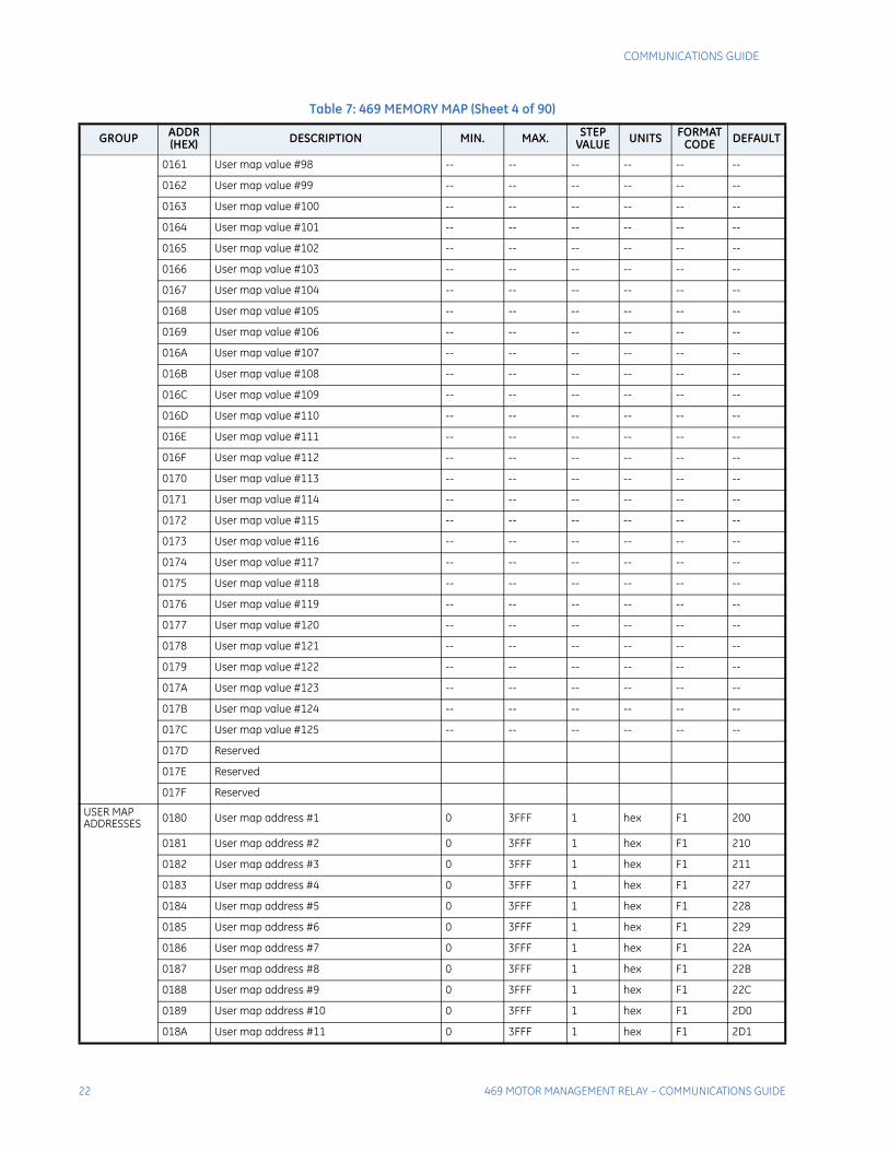
USER MAP ADDRESSES 0180 User map address #1 0 3FFF 1 hex F1 200
0181 User map address #2 0 3FFF 1 hex F1 210
0182 User map address #3 0 3FFF 1 hex F1 211
0183 User map address #4 0 3FFF 1 hex F1 227
0184 User map address #5 0 3FFF 1 hex F1 228
0185 User map address #6 0 3FFF 1 hex F1 229
0186 User map address #7 0 3FFF 1 hex F1 22A
0187 User map address #8 0 3FFF 1 hex F1 22B
0188 User map address #9 0 3FFF 1 hex F1 22C
0189 User map address #10 0 3FFF 1 hex F1 2D0
018A User map address #11 0 3FFF 1 hex F1 2D1
Table 7: 469 MEMORY MAP (Sheet 4 of 90)
GROUP ADDR(HEX) DESCRIPTION MIN. MAX. STEP
VALUE UNITS FORMATCODE DEFAULT
COMMUNICATIONS GUIDE
469 MOTOR MANAGEMENT RELAY – COMMUNICATIONS GUIDE 23
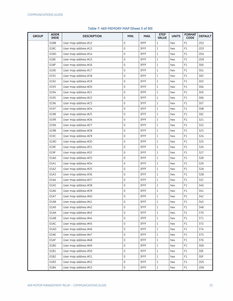
018B User map address #12 0 3FFF 1 hex F1 2D2
018C User map address #13 0 3FFF 1 hex F1 2D3
018D User map address #14 0 3FFF 1 hex F1 2D4
018E User map address #15 0 3FFF 1 hex F1 2D9
018F User map address #16 0 3FFF 1 hex F1 300
0190 User map address #17 0 3FFF 1 hex F1 301
0191 User map address #18 0 3FFF 1 hex F1 302
0192 User map address #19 0 3FFF 1 hex F1 303
0193 User map address #20 0 3FFF 1 hex F1 304
0194 User map address #21 0 3FFF 1 hex F1 305
0195 User map address #22 0 3FFF 1 hex F1 306
0196 User map address #23 0 3FFF 1 hex F1 307
0197 User map address #24 0 3FFF 1 hex F1 30B
0198 User map address #25 0 3FFF 1 hex F1 30C
0199 User map address #26 0 3FFF 1 hex F1 321
019A User map address #27 0 3FFF 1 hex F1 322
019B User map address #28 0 3FFF 1 hex F1 323
019C User map address #29 0 3FFF 1 hex F1 324
019D User map address #30 0 3FFF 1 hex F1 325
019E User map address #31 0 3FFF 1 hex F1 326
019F User map address #32 0 3FFF 1 hex F1 327
01A0 User map address #33 0 3FFF 1 hex F1 328
01A1 User map address #34 0 3FFF 1 hex F1 329
01A2 User map address #35 0 3FFF 1 hex F1 32A
01A3 User map address #36 0 3FFF 1 hex F1 32B
01A4 User map address #37 0 3FFF 1 hex F1 32C
01A5 User map address #38 0 3FFF 1 hex F1 340
01A6 User map address #39 0 3FFF 1 hex F1 341
01A7 User map address #40 0 3FFF 1 hex F1 342
01A8 User map address #41 0 3FFF 1 hex F1 343
01A9 User map address #42 0 3FFF 1 hex F1 348
01AA User map address #43 0 3FFF 1 hex F1 370
01AB User map address #44 0 3FFF 1 hex F1 371
01AC User map address #45 0 3FFF 1 hex F1 372
01AD User map address #46 0 3FFF 1 hex F1 374
01AE User map address #47 0 3FFF 1 hex F1 375
01AF User map address #48 0 3FFF 1 hex F1 376
01B0 User map address #49 0 3FFF 1 hex F1 30D
01B1 User map address #50 0 3FFF 1 hex F1 30E
01B2 User map address #51 0 3FFF 1 hex F1 30F
01B3 User map address #52 0 3FFF 1 hex F1 2D5
01B4 User map address #53 0 3FFF 1 hex F1 2D6
Table 7: 469 MEMORY MAP (Sheet 5 of 90)
GROUP ADDR(HEX) DESCRIPTION MIN. MAX. STEP
VALUE UNITS FORMATCODE DEFAULT
24 469 MOTOR MANAGEMENT RELAY – COMMUNICATIONS GUIDE
COMMUNICATIONS GUIDE
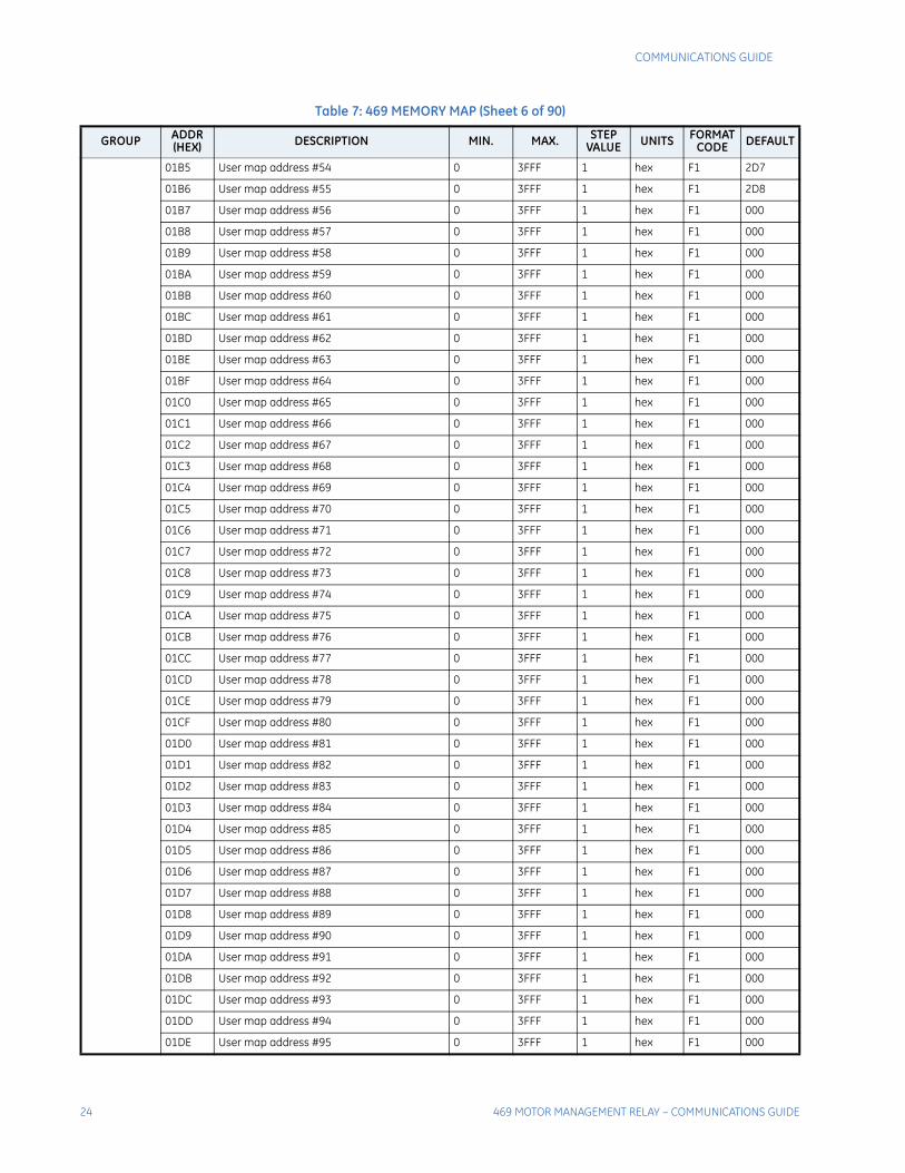
01B5 User map address #54 0 3FFF 1 hex F1 2D7
01B6 User map address #55 0 3FFF 1 hex F1 2D8
01B7 User map address #56 0 3FFF 1 hex F1 000
01B8 User map address #57 0 3FFF 1 hex F1 000
01B9 User map address #58 0 3FFF 1 hex F1 000
01BA User map address #59 0 3FFF 1 hex F1 000
01BB User map address #60 0 3FFF 1 hex F1 000
01BC User map address #61 0 3FFF 1 hex F1 000
01BD User map address #62 0 3FFF 1 hex F1 000
01BE User map address #63 0 3FFF 1 hex F1 000
01BF User map address #64 0 3FFF 1 hex F1 000
01C0 User map address #65 0 3FFF 1 hex F1 000
01C1 User map address #66 0 3FFF 1 hex F1 000
01C2 User map address #67 0 3FFF 1 hex F1 000
01C3 User map address #68 0 3FFF 1 hex F1 000
01C4 User map address #69 0 3FFF 1 hex F1 000
01C5 User map address #70 0 3FFF 1 hex F1 000
01C6 User map address #71 0 3FFF 1 hex F1 000
01C7 User map address #72 0 3FFF 1 hex F1 000
01C8 User map address #73 0 3FFF 1 hex F1 000
01C9 User map address #74 0 3FFF 1 hex F1 000
01CA User map address #75 0 3FFF 1 hex F1 000
01CB User map address #76 0 3FFF 1 hex F1 000
01CC User map address #77 0 3FFF 1 hex F1 000
01CD User map address #78 0 3FFF 1 hex F1 000
01CE User map address #79 0 3FFF 1 hex F1 000
01CF User map address #80 0 3FFF 1 hex F1 000
01D0 User map address #81 0 3FFF 1 hex F1 000
01D1 User map address #82 0 3FFF 1 hex F1 000
01D2 User map address #83 0 3FFF 1 hex F1 000
01D3 User map address #84 0 3FFF 1 hex F1 000
01D4 User map address #85 0 3FFF 1 hex F1 000
01D5 User map address #86 0 3FFF 1 hex F1 000
01D6 User map address #87 0 3FFF 1 hex F1 000
01D7 User map address #88 0 3FFF 1 hex F1 000
01D8 User map address #89 0 3FFF 1 hex F1 000
01D9 User map address #90 0 3FFF 1 hex F1 000
01DA User map address #91 0 3FFF 1 hex F1 000
01DB User map address #92 0 3FFF 1 hex F1 000
01DC User map address #93 0 3FFF 1 hex F1 000
01DD User map address #94 0 3FFF 1 hex F1 000
01DE User map address #95 0 3FFF 1 hex F1 000
Table 7: 469 MEMORY MAP (Sheet 6 of 90)
GROUP ADDR(HEX) DESCRIPTION MIN. MAX. STEP
VALUE UNITS FORMATCODE DEFAULT
COMMUNICATIONS GUIDE
469 MOTOR MANAGEMENT RELAY – COMMUNICATIONS GUIDE 25
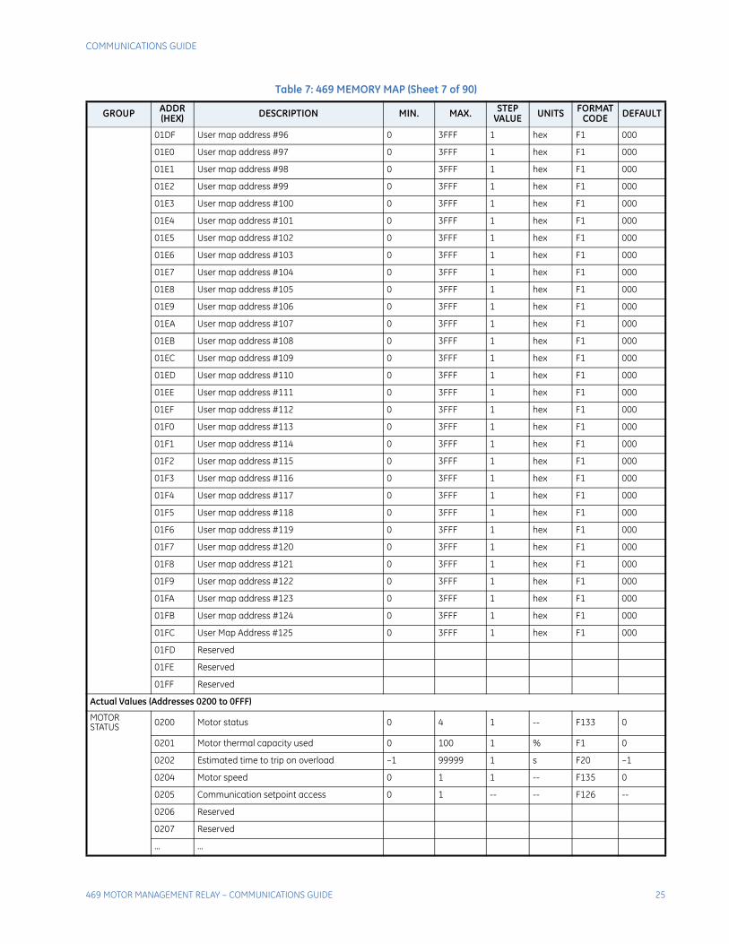
01DF User map address #96 0 3FFF 1 hex F1 000
01E0 User map address #97 0 3FFF 1 hex F1 000
01E1 User map address #98 0 3FFF 1 hex F1 000
01E2 User map address #99 0 3FFF 1 hex F1 000
01E3 User map address #100 0 3FFF 1 hex F1 000
01E4 User map address #101 0 3FFF 1 hex F1 000
01E5 User map address #102 0 3FFF 1 hex F1 000
01E6 User map address #103 0 3FFF 1 hex F1 000
01E7 User map address #104 0 3FFF 1 hex F1 000
01E8 User map address #105 0 3FFF 1 hex F1 000
01E9 User map address #106 0 3FFF 1 hex F1 000
01EA User map address #107 0 3FFF 1 hex F1 000
01EB User map address #108 0 3FFF 1 hex F1 000
01EC User map address #109 0 3FFF 1 hex F1 000
01ED User map address #110 0 3FFF 1 hex F1 000
01EE User map address #111 0 3FFF 1 hex F1 000
01EF User map address #112 0 3FFF 1 hex F1 000
01F0 User map address #113 0 3FFF 1 hex F1 000
01F1 User map address #114 0 3FFF 1 hex F1 000
01F2 User map address #115 0 3FFF 1 hex F1 000
01F3 User map address #116 0 3FFF 1 hex F1 000
01F4 User map address #117 0 3FFF 1 hex F1 000
01F5 User map address #118 0 3FFF 1 hex F1 000
01F6 User map address #119 0 3FFF 1 hex F1 000
01F7 User map address #120 0 3FFF 1 hex F1 000
01F8 User map address #121 0 3FFF 1 hex F1 000
01F9 User map address #122 0 3FFF 1 hex F1 000
01FA User map address #123 0 3FFF 1 hex F1 000
01FB User map address #124 0 3FFF 1 hex F1 000
01FC User Map Address #125 0 3FFF 1 hex F1 000
01FD Reserved
01FE Reserved
01FF Reserved
Actual Values (Addresses 0200 to 0FFF)
MOTORSTATUS 0200 Motor status 0 4 1 -- F133 0
0201 Motor thermal capacity used 0 100 1 % F1 0
0202 Estimated time to trip on overload –1 99999 1 s F20 –1
0204 Motor speed 0 1 1 -- F135 0
0205 Communication setpoint access 0 1 -- -- F126 --
0206 Reserved
0207 Reserved
... ...
Table 7: 469 MEMORY MAP (Sheet 7 of 90)
GROUP ADDR(HEX) DESCRIPTION MIN. MAX. STEP
VALUE UNITS FORMATCODE DEFAULT
26 469 MOTOR MANAGEMENT RELAY – COMMUNICATIONS GUIDE
COMMUNICATIONS GUIDE
020F Reserved
SYSTEMSTATUS 0210 General status 0 65535 1 -- F140 0
0211 Output relay status 0 63 1 -- F141 0
0212 Reserved
0213 Reserved
... ...
021F Reserved
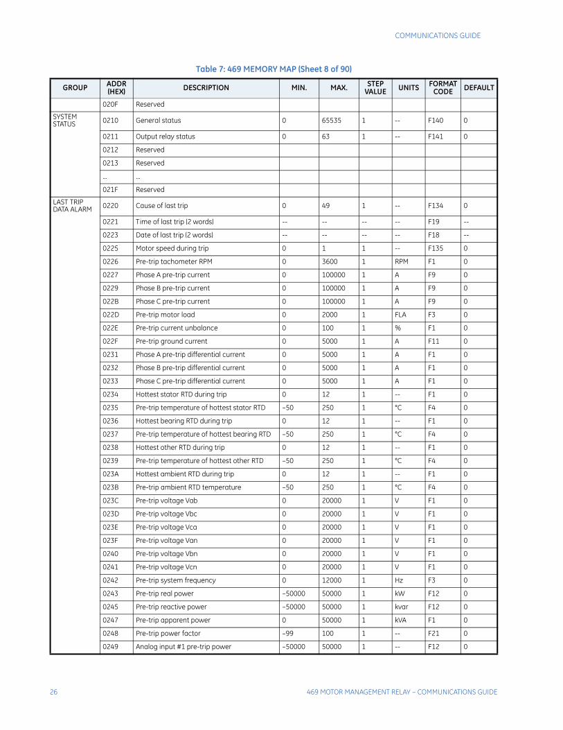
LAST TRIP DATA ALARM 0220 Cause of last trip 0 49 1 -- F134 0
0221 Time of last trip (2 words) -- -- -- -- F19 --
0223 Date of last trip (2 words) -- -- -- -- F18 --
0225 Motor speed during trip 0 1 1 -- F135 0
0226 Pre-trip tachometer RPM 0 3600 1 RPM F1 0
0227 Phase A pre-trip current 0 100000 1 A F9 0
0229 Phase B pre-trip current 0 100000 1 A F9 0
022B Phase C pre-trip current 0 100000 1 A F9 0
022D Pre-trip motor load 0 2000 1 FLA F3 0
022E Pre-trip current unbalance 0 100 1 % F1 0
022F Pre-trip ground current 0 5000 1 A F11 0
0231 Phase A pre-trip differential current 0 5000 1 A F1 0
0232 Phase B pre-trip differential current 0 5000 1 A F1 0
0233 Phase C pre-trip differential current 0 5000 1 A F1 0
0234 Hottest stator RTD during trip 0 12 1 -- F1 0
0235 Pre-trip temperature of hottest stator RTD –50 250 1 °C F4 0
0236 Hottest bearing RTD during trip 0 12 1 -- F1 0
0237 Pre-trip temperature of hottest bearing RTD –50 250 1 °C F4 0
0238 Hottest other RTD during trip 0 12 1 -- F1 0
0239 Pre-trip temperature of hottest other RTD –50 250 1 °C F4 0
023A Hottest ambient RTD during trip 0 12 1 -- F1 0
023B Pre-trip ambient RTD temperature –50 250 1 °C F4 0
023C Pre-trip voltage Vab 0 20000 1 V F1 0
023D Pre-trip voltage Vbc 0 20000 1 V F1 0
023E Pre-trip voltage Vca 0 20000 1 V F1 0
023F Pre-trip voltage Van 0 20000 1 V F1 0
0240 Pre-trip voltage Vbn 0 20000 1 V F1 0
0241 Pre-trip voltage Vcn 0 20000 1 V F1 0
0242 Pre-trip system frequency 0 12000 1 Hz F3 0
0243 Pre-trip real power –50000 50000 1 kW F12 0
0245 Pre-trip reactive power –50000 50000 1 kvar F12 0
0247 Pre-trip apparent power 0 50000 1 kVA F1 0
0248 Pre-trip power factor –99 100 1 -- F21 0
0249 Analog input #1 pre-trip power –50000 50000 1 -- F12 0
Table 7: 469 MEMORY MAP (Sheet 8 of 90)
GROUP ADDR(HEX) DESCRIPTION MIN. MAX. STEP
VALUE UNITS FORMATCODE DEFAULT
COMMUNICATIONS GUIDE
469 MOTOR MANAGEMENT RELAY – COMMUNICATIONS GUIDE 27
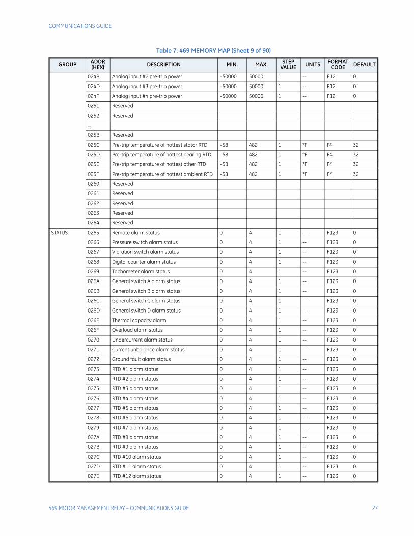
024B Analog input #2 pre-trip power –50000 50000 1 -- F12 0
024D Analog input #3 pre-trip power –50000 50000 1 -- F12 0
024F Analog input #4 pre-trip power –50000 50000 1 -- F12 0
0251 Reserved
0252 Reserved
... ...
025B Reserved
025C Pre-trip temperature of hottest stator RTD –58 482 1 °F F4 32
025D Pre-trip temperature of hottest bearing RTD –58 482 1 °F F4 32
025E Pre-trip temperature of hottest other RTD –58 482 1 °F F4 32
025F Pre-trip temperature of hottest ambient RTD –58 482 1 °F F4 32
0260 Reserved
0261 Reserved
0262 Reserved
0263 Reserved
0264 Reserved
STATUS 0265 Remote alarm status 0 4 1 -- F123 0
0266 Pressure switch alarm status 0 4 1 -- F123 0
0267 Vibration switch alarm status 0 4 1 -- F123 0
0268 Digital counter alarm status 0 4 1 -- F123 0
0269 Tachometer alarm status 0 4 1 -- F123 0
026A General switch A alarm status 0 4 1 -- F123 0
026B General switch B alarm status 0 4 1 -- F123 0
026C General switch C alarm status 0 4 1 -- F123 0
026D General switch D alarm status 0 4 1 -- F123 0
026E Thermal capacity alarm 0 4 1 -- F123 0
026F Overload alarm status 0 4 1 -- F123 0
0270 Undercurrent alarm status 0 4 1 -- F123 0
0271 Current unbalance alarm status 0 4 1 -- F123 0
0272 Ground fault alarm status 0 4 1 -- F123 0
0273 RTD #1 alarm status 0 4 1 -- F123 0
0274 RTD #2 alarm status 0 4 1 -- F123 0
0275 RTD #3 alarm status 0 4 1 -- F123 0
0276 RTD #4 alarm status 0 4 1 -- F123 0
0277 RTD #5 alarm status 0 4 1 -- F123 0
0278 RTD #6 alarm status 0 4 1 -- F123 0
0279 RTD #7 alarm status 0 4 1 -- F123 0
027A RTD #8 alarm status 0 4 1 -- F123 0
027B RTD #9 alarm status 0 4 1 -- F123 0
027C RTD #10 alarm status 0 4 1 -- F123 0
027D RTD #11 alarm status 0 4 1 -- F123 0
027E RTD #12 alarm status 0 4 1 -- F123 0
Table 7: 469 MEMORY MAP (Sheet 9 of 90)
GROUP ADDR(HEX) DESCRIPTION MIN. MAX. STEP
VALUE UNITS FORMATCODE DEFAULT
28 469 MOTOR MANAGEMENT RELAY – COMMUNICATIONS GUIDE
COMMUNICATIONS GUIDE
027F Open RTD sensor alarm status 0 4 1 -- F123 0
0280 Short sensor / low temperature alarm status 0 4 1 -- F123 0
0281 Undervoltage alarm status 0 4 1 -- F123 0
0282 Overvoltage alarm status 0 4 1 -- F123 0
0283 System frequency alarm status 0 4 1 -- F123 0
0284 Power factor alarm status 0 4 1 -- F123 0
0285 Reactive power alarm status 0 4 1 -- F123 0
0286 Underpower alarm status 0 4 1 -- F123 0
0287 Trip counter alarm status 0 4 1 -- F123 0
0288 Starter failure alarm 0 4 1 -- F123 0
0289 Current demand alarm status 0 4 1 -- F123 0
028A kW demand alarm status 0 4 1 -- F123 0
028B kvar demand alarm status 0 4 1 -- F123 0
028C kVA demand alarm status 0 4 1 -- F123 0
028D Analog input 1 alarm status 0 4 1 -- F123 0
028E Analog input 2 alarm status 0 4 1 -- F123 0
028F Analog input 3 alarm status 0 4 1 -- F123 0
0290 Analog input 4 alarm status 0 4 1 -- F123 0
0291 Reverse power alarm status 0 4 1 -- F123 0
0292 RTD #1 high alarm status 0 4 1 -- F123 0
0293 RTD #2 high alarm status 0 4 1 -- F123 0
0294 RTD #3 high alarm status 0 4 1 -- F123 0
0295 RTD #4 high alarm status 0 4 1 -- F123 0
0296 RTD #5 high alarm status 0 4 1 -- F123 0
0297 RTD #6 high alarm status 0 4 1 -- F123 0
0298 RTD #7 high alarm status 0 4 1 -- F123 0
0299 RTD #8 high alarm status 0 4 1 -- F123 0
029A RTD #9 high alarm status 0 4 1 -- F123 0
029B RTD #10 high alarm status 0 4 1 -- F123 0
029C RTD #11 high alarm status 0 4 1 -- F123 0
029D RTD #12 high alarm status 0 4 1 -- F123 0
029E Analog difference 1-2 alarm status 0 4 1 -- F123 0
029F Analog difference 3-4 alarm status 0 4 1 -- F123 0
02A0 Overtorque alarm status 0 4 1 -- F123 0
02A1 Reserved
02A2 Reserved
...
02AE Loss of Comms Alarm Status 0 4 1 -- F123 0
02AF Self test alarm 0 FFFF 1 -- -- 0
START BLOCKS 02B0 Overload lockout block 0 500 1 minutes F1 0
02B1 Start inhibit block lockout time 0 500 1 minutes F1 0
02B2 Starts/hour block lockout time 0 60 1 minutes F1 0
Table 7: 469 MEMORY MAP (Sheet 10 of 90)
GROUP ADDR(HEX) DESCRIPTION MIN. MAX. STEP
VALUE UNITS FORMATCODE DEFAULT
COMMUNICATIONS GUIDE
469 MOTOR MANAGEMENT RELAY – COMMUNICATIONS GUIDE 29
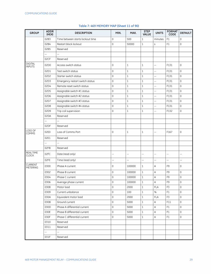
02B3 Time between starts lockout time 0 500 1 minutes F1 0
02B4 Restart block lockout 0 50000 1 s F1 0
02B5 Reserved
-- --
02CF Reserved
DIGITAL INPUTS 02D0 Access switch status 0 1 1 -- F131 0
02D1 Test switch status 0 1 1 -- F131 0
02D2 Starter switch status 0 1 1 -- F131 0
02D3 Emergency restart switch status 0 1 1 -- F131 0
02D4 Remote reset switch status 0 1 1 -- F131 0
02D5 Assignable switch #1 status 0 1 1 -- F131 0
02D6 Assignable switch #2 status 0 1 1 -- F131 0
02D7 Assignable switch #3 status 0 1 1 -- F131 0
02D8 Assignable switch #4 status 0 1 1 -- F131 0
02D9 Trip coil supervision 0 1 1 -- F132 0
02DA Reserved
-- --
02DF Reserved
LOSS OF COMMS 02E0 Loss of Comms Port 0 1 1 -- F167 0
02E1 Reserved
-- --
02FB Reserved
REAL TIME CLOCK 02FC Date (read only) -- -- -- -- -- --
02FE Time (read only) -- -- -- -- -- --
CURRENT METERING 0300 Phase A current 0 100000 1 A F9 0
0302 Phase B current 0 100000 1 A F9 0
0304 Phase C current 0 100000 1 A F9 0
0306 Average phase current 0 100000 1 A F9 0
0308 Motor load 0 2000 1 FLA F3 0
0309 Current unbalance 0 100 1 % F1 0
030A Equivalent motor load 0 2000 1 FLA F3 0
030B Ground current 0 5000 1 A F11 0
030D Phase A differential current 0 5000 1 A F1 0
030E Phase B differential current 0 5000 1 A F1 0
030F Phase C differential current 0 5000 1 A F1 0
0310 Reserved
0311 Reserved
-- --
031F Reserved
Table 7: 469 MEMORY MAP (Sheet 11 of 90)
GROUP ADDR(HEX) DESCRIPTION MIN. MAX. STEP
VALUE UNITS FORMATCODE DEFAULT
30 469 MOTOR MANAGEMENT RELAY – COMMUNICATIONS GUIDE
COMMUNICATIONS GUIDE
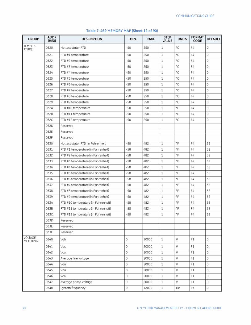
TEMPER-ATURE 0320 Hottest stator RTD –50 250 1 °C F4 0
0321 RTD #1 temperature –50 250 1 °C F4 0
0322 RTD #2 temperature –50 250 1 °C F4 0
0323 RTD #3 temperature –50 250 1 °C F4 0
0324 RTD #4 temperature –50 250 1 °C F4 0
0325 RTD #5 temperature –50 250 1 °C F4 0
0326 RTD #6 temperature –50 250 1 °C F4 0
0327 RTD #7 temperature –50 250 1 °C F4 0
0328 RTD #8 temperature –50 250 1 °C F4 0
0329 RTD #9 temperature –50 250 1 °C F4 0
032A RTD #10 temperature –50 250 1 °C F4 0
032B RTD #11 temperature –50 250 1 °C F4 0
032C RTD #12 temperature –50 250 1 °C F4 0
032D Reserved
032E Reserved
032F Reserved
0330 Hottest stator RTD (in Fahrenheit) –58 482 1 °F F4 32
0331 RTD #1 temperature (in Fahrenheit) –58 482 1 °F F4 32
0332 RTD #2 temperature (in Fahrenheit) –58 482 1 °F F4 32
0333 RTD #3 temperature (in Fahrenheit) –58 482 1 °F F4 32
0334 RTD #4 temperature (in Fahrenheit) –58 482 1 °F F4 32
0335 RTD #5 temperature (in Fahrenheit) –58 482 1 °F F4 32
0336 RTD #6 temperature (in Fahrenheit) –58 482 1 °F F4 32
0337 RTD #7 temperature (in Fahrenheit) –58 482 1 °F F4 32
0338 RTD #8 temperature (in Fahrenheit) –58 482 1 °F F4 32
0339 RTD #9 temperature (in Fahrenheit) –58 482 1 °F F4 32
033A RTD #10 temperature (in Fahrenheit) –58 482 1 °F F4 32
033B RTD #11 temperature (in Fahrenheit) –58 482 1 °F F4 32
033C RTD #12 temperature (in Fahrenheit) –58 482 1 °F F4 32
033D Reserved
033E Reserved
033F Reserved
VOLTAGE METERING 0340 Vab 0 20000 1 V F1 0
0341 Vbc 0 20000 1 V F1 0
0342 Vca 0 20000 1 V F1 0
0343 Average line voltage 0 20000 1 V F1 0
0344 Van 0 20000 1 V F1 0
0345 Vbn 0 20000 1 V F1 0
0346 Vcn 0 20000 1 V F1 0
0347 Average phase voltage 0 20000 1 V F1 0
0348 System frequency 0 12000 1 Hz F3 0
Table 7: 469 MEMORY MAP (Sheet 12 of 90)
GROUP ADDR(HEX) DESCRIPTION MIN. MAX. STEP
VALUE UNITS FORMATCODE DEFAULT
COMMUNICATIONS GUIDE
469 MOTOR MANAGEMENT RELAY – COMMUNICATIONS GUIDE 31
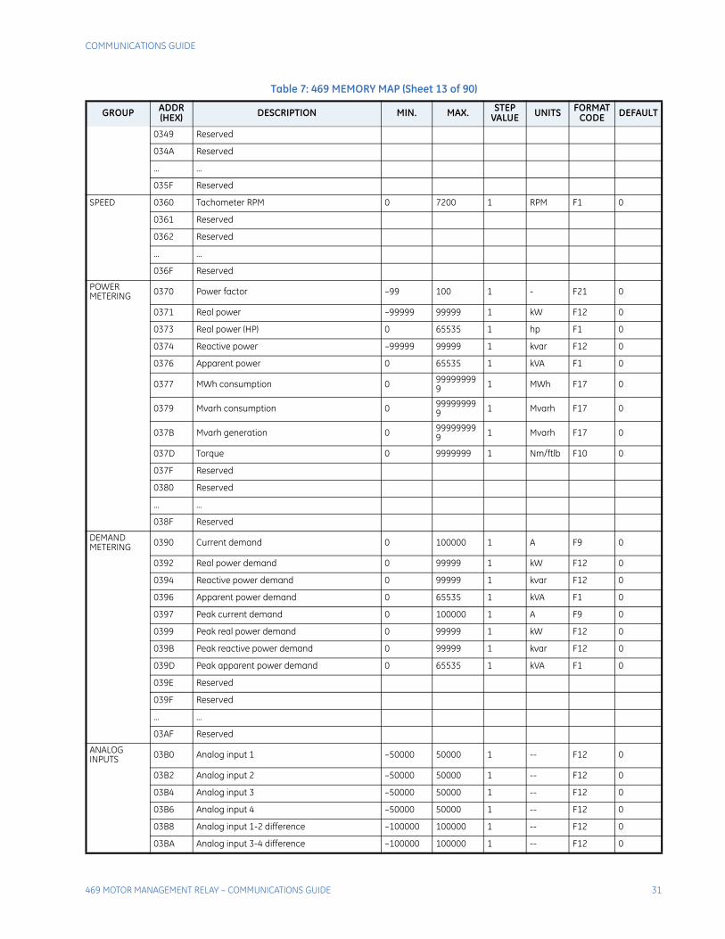
0349 Reserved
034A Reserved
... ...
035F Reserved
SPEED 0360 Tachometer RPM 0 7200 1 RPM F1 0
0361 Reserved
0362 Reserved
... ...
036F Reserved
POWER METERING 0370 Power factor –99 100 1 - F21 0
0371 Real power –99999 99999 1 kW F12 0
0373 Real power (HP) 0 65535 1 hp F1 0
0374 Reactive power –99999 99999 1 kvar F12 0
0376 Apparent power 0 65535 1 kVA F1 0
0377 MWh consumption 0 999999999 1 MWh F17 0
0379 Mvarh consumption 0 999999999 1 Mvarh F17 0
037B Mvarh generation 0 999999999 1 Mvarh F17 0
037D Torque 0 9999999 1 Nm/ftlb F10 0
037F Reserved
0380 Reserved
... ...
038F Reserved
DEMAND METERING 0390 Current demand 0 100000 1 A F9 0
0392 Real power demand 0 99999 1 kW F12 0
0394 Reactive power demand 0 99999 1 kvar F12 0
0396 Apparent power demand 0 65535 1 kVA F1 0
0397 Peak current demand 0 100000 1 A F9 0
0399 Peak real power demand 0 99999 1 kW F12 0
039B Peak reactive power demand 0 99999 1 kvar F12 0
039D Peak apparent power demand 0 65535 1 kVA F1 0
039E Reserved
039F Reserved
... ...
03AF Reserved
ANALOG INPUTS 03B0 Analog input 1 –50000 50000 1 -- F12 0
03B2 Analog input 2 –50000 50000 1 -- F12 0
03B4 Analog input 3 –50000 50000 1 -- F12 0
03B6 Analog input 4 –50000 50000 1 -- F12 0
03B8 Analog input 1-2 difference –100000 100000 1 -- F12 0
03BA Analog input 3-4 difference –100000 100000 1 -- F12 0
Table 7: 469 MEMORY MAP (Sheet 13 of 90)
GROUP ADDR(HEX) DESCRIPTION MIN. MAX. STEP
VALUE UNITS FORMATCODE DEFAULT
32 469 MOTOR MANAGEMENT RELAY – COMMUNICATIONS GUIDE
COMMUNICATIONS GUIDE
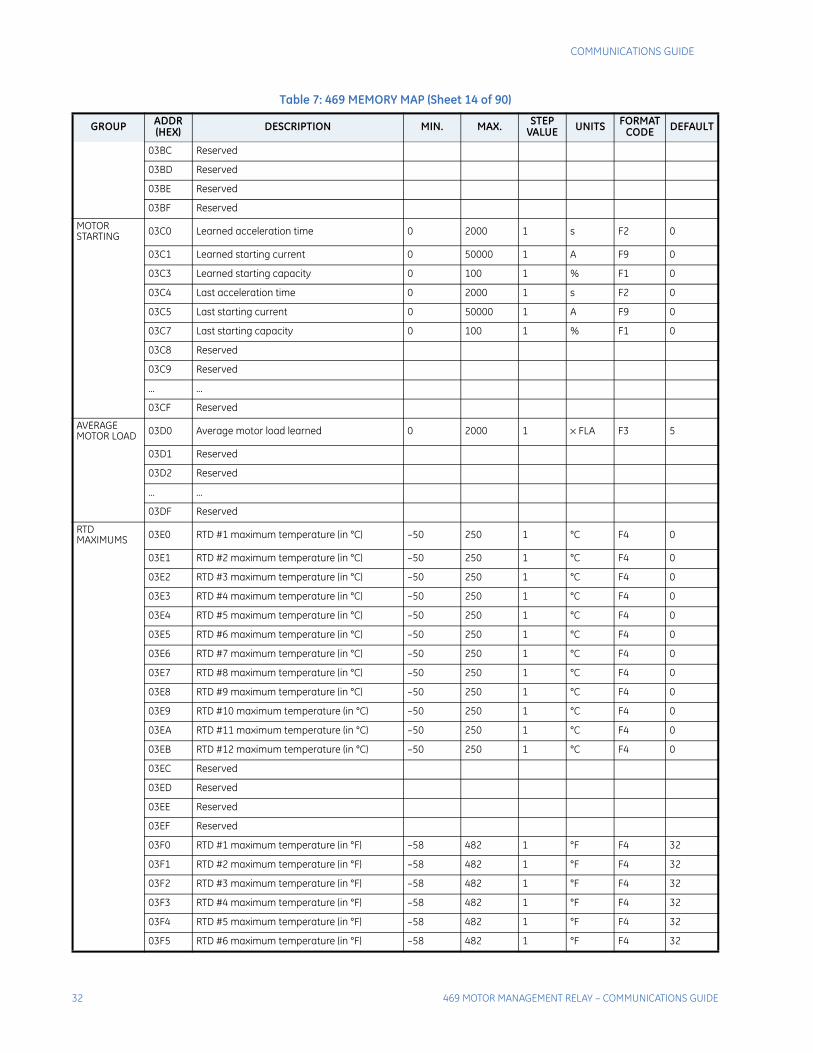
03BC Reserved
03BD Reserved
03BE Reserved
03BF Reserved
MOTOR STARTING 03C0 Learned acceleration time 0 2000 1 s F2 0
03C1 Learned starting current 0 50000 1 A F9 0
03C3 Learned starting capacity 0 100 1 % F1 0
03C4 Last acceleration time 0 2000 1 s F2 0
03C5 Last starting current 0 50000 1 A F9 0
03C7 Last starting capacity 0 100 1 % F1 0
03C8 Reserved
03C9 Reserved
... ...
03CF Reserved
AVERAGE MOTOR LOAD 03D0 Average motor load learned 0 2000 1 × FLA F3 5
03D1 Reserved
03D2 Reserved
... ...
03DF Reserved
RTDMAXIMUMS 03E0 RTD #1 maximum temperature (in °C) –50 250 1 °C F4 0
03E1 RTD #2 maximum temperature (in °C) –50 250 1 °C F4 0
03E2 RTD #3 maximum temperature (in °C) –50 250 1 °C F4 0
03E3 RTD #4 maximum temperature (in °C) –50 250 1 °C F4 0
03E4 RTD #5 maximum temperature (in °C) –50 250 1 °C F4 0
03E5 RTD #6 maximum temperature (in °C) –50 250 1 °C F4 0
03E6 RTD #7 maximum temperature (in °C) –50 250 1 °C F4 0
03E7 RTD #8 maximum temperature (in °C) –50 250 1 °C F4 0
03E8 RTD #9 maximum temperature (in °C) –50 250 1 °C F4 0
03E9 RTD #10 maximum temperature (in °C) –50 250 1 °C F4 0
03EA RTD #11 maximum temperature (in °C) –50 250 1 °C F4 0
03EB RTD #12 maximum temperature (in °C) –50 250 1 °C F4 0
03EC Reserved
03ED Reserved
03EE Reserved
03EF Reserved
03F0 RTD #1 maximum temperature (in °F) –58 482 1 °F F4 32
03F1 RTD #2 maximum temperature (in °F) –58 482 1 °F F4 32
03F2 RTD #3 maximum temperature (in °F) –58 482 1 °F F4 32
03F3 RTD #4 maximum temperature (in °F) –58 482 1 °F F4 32
03F4 RTD #5 maximum temperature (in °F) –58 482 1 °F F4 32
03F5 RTD #6 maximum temperature (in °F) –58 482 1 °F F4 32
Table 7: 469 MEMORY MAP (Sheet 14 of 90)
GROUP ADDR(HEX) DESCRIPTION MIN. MAX. STEP
VALUE UNITS FORMATCODE DEFAULT
COMMUNICATIONS GUIDE
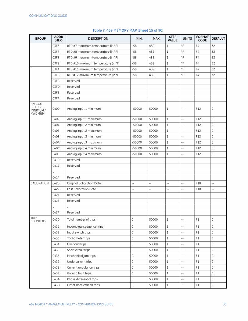
469 MOTOR MANAGEMENT RELAY – COMMUNICATIONS GUIDE 33
03F6 RTD #7 maximum temperature (in °F) –58 482 1 °F F4 32
03F7 RTD #8 maximum temperature (in °F) –58 482 1 °F F4 32
03F8 RTD #9 maximum temperature (in °F) –58 482 1 °F F4 32
03F9 RTD #10 maximum temperature (in °F) –58 482 1 °F F4 32
03FA RTD #11 maximum temperature (in °F) –58 482 1 °F F4 32
03FB RTD #12 maximum temperature (in °F) –58 482 1 °F F4 32
03FC Reserved
03FD Reserved
03FE Reserved
03FF Reserved
ANALOG INPUTSMINIMUM / MAXIMUM
0400 Analog input 1 minimum –50000 50000 1 -- F12 0
0402 Analog input 1 maximum –50000 50000 1 -- F12 0
0404 Analog input 2 minimum –50000 50000 1 -- F12 0
0406 Analog input 2 maximum –50000 50000 1 -- F12 0
0408 Analog input 3 minimum –50000 50000 1 -- F12 0
040A Analog input 3 maximum –50000 50000 1 -- F12 0
040C Analog input 4 minimum –50000 50000 1 -- F12 0
040E Analog input 4 maximum –50000 50000 1 -- F12 0
0410 Reserved
0411 Reserved
...
041F Reserved
CALIBRATION 0420 Original Calibration Date -- -- -- -- F18 --
0422 Last Calibration Date -- -- -- -- F18 --
0424 Reserved
0425 Reserved
... ...
042F Reserved
TRIP COUNTERS 0430 Total number of trips 0 50000 1 -- F1 0
0431 Incomplete sequence trips 0 50000 1 -- F1 0
0432 Input switch trips 0 50000 1 -- F1 0
0433 Tachometer trips 0 50000 1 -- F1 0
0434 Overload trips 0 50000 1 -- F1 0
0435 Short circuit trips 0 50000 1 -- F1 0
0436 Mechanical jam trips 0 50000 1 -- F1 0
0437 Undercurrent trips 0 50000 1 -- F1 0
0438 Current unbalance trips 0 50000 1 -- F1 0
0439 Ground fault trips 0 50000 1 -- F1 0
043A Phase differential trips 0 50000 1 -- F1 0
043B Motor acceleration trips 0 50000 1 -- F1 0
Table 7: 469 MEMORY MAP (Sheet 15 of 90)
GROUP ADDR(HEX) DESCRIPTION MIN. MAX. STEP
VALUE UNITS FORMATCODE DEFAULT
34 469 MOTOR MANAGEMENT RELAY – COMMUNICATIONS GUIDE
COMMUNICATIONS GUIDE
043C Stator RTD trips 0 50000 1 -- F1 0
043D Bearing RTD trips 0 50000 1 -- F1 0
043E Other RTD trips 0 50000 1 -- F1 0
043F Ambient RTD trips 0 50000 1 -- F1 0
0440 Undervoltage trips 0 50000 1 -- F1 0
0441 Overvoltage trips 0 50000 1 -- F1 0
0442 Voltage phase reversal trips 0 50000 1 -- F1 0
0443 Voltage frequency trips 0 50000 1 -- F1 0
0444 Power factor trips 0 50000 1 -- F1 0
0445 Reactive power trips 0 50000 1 -- F1 0
0446 Underpower trips 0 50000 1 -- F1 0
0447 Analog input 1 trips 0 50000 1 -- F1 0
0448 Analog input 2 trips 0 50000 1 -- F1 0
0449 Analog input 3 trips 0 50000 1 -- F1 0
044A Analog input 4 trips 0 50000 1 -- F1 0
044B Reverse power trips 0 50000 1 -- F1 0
044C Analog inputs difference 1-2 trips 0 50000 1 -- F1 0
044D Analog inputs difference 3-4 trips 0 50000 1 -- F1 0
044E Loss of Comms Trips 0 50000 1 -- F1 0
044F Reserved
... ...
046F Reserved
GENERAL COUNTERS 0470 Number of motor starts 0 50000 1 -- F1 0
0471 Number of emergency restarts 0 50000 1 -- F1 0
0472 Number of starter operations 0 50000 1 -- F1 0
0473 Digital counter 0 1000000000 1 -- F9 0
0475 Reserved
0475 Reserved
... ...
049F Reserved
TIMERS 04A0 Motor running hours 1 100000 1 hours F9 0
04A2 Time between starts timer 0 500 1 minutes F1 0
04A3 Start timer 1 0 60 1 minutes F1 0
04A4 Start timer 2 0 60 1 minutes F1 0
04A5 Start timer 3 0 60 1 minutes F1 0
04A6 Start timer 4 0 60 1 minutes F1 0
04A7 Start timer 5 0 60 1 minutes F1 0
04A8 Reserved
04A9 Reserved
... ...
04BF Reserved
Table 7: 469 MEMORY MAP (Sheet 16 of 90)
GROUP ADDR(HEX) DESCRIPTION MIN. MAX. STEP
VALUE UNITS FORMATCODE DEFAULT
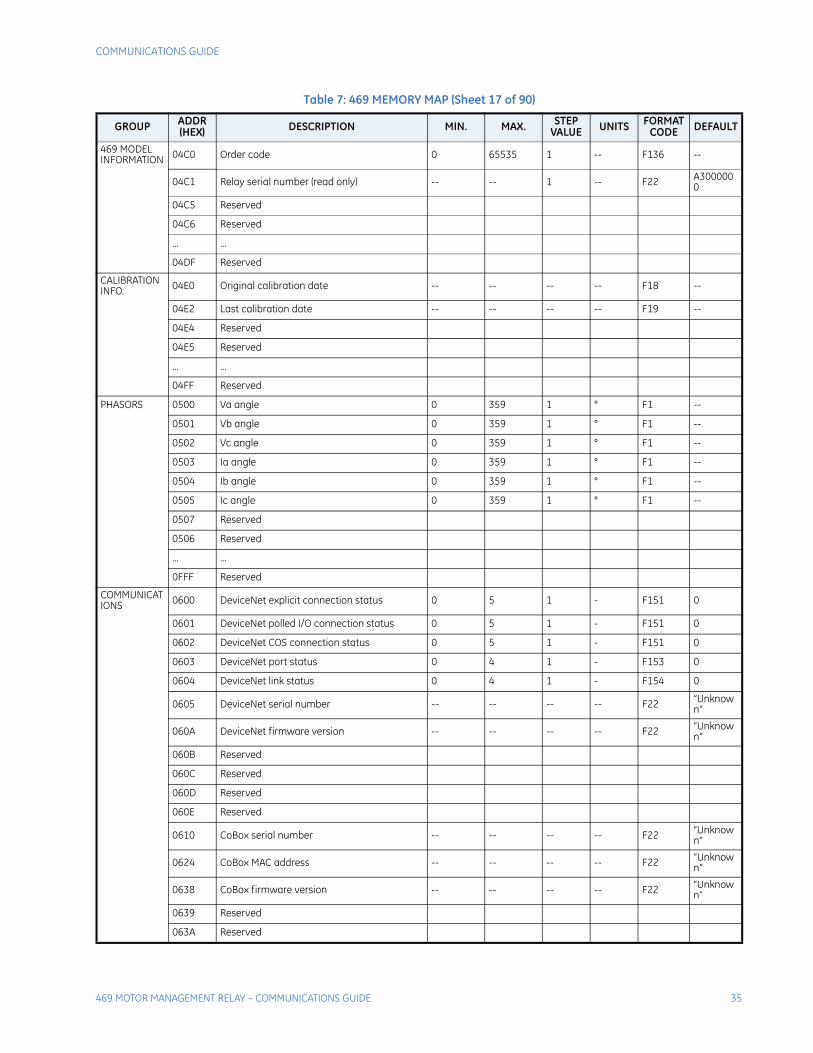
COMMUNICATIONS GUIDE
469 MOTOR MANAGEMENT RELAY – COMMUNICATIONS GUIDE 35
469 MODEL INFORMATION 04C0 Order code 0 65535 1 -- F136 --
04C1 Relay serial number (read only) -- -- 1 -- F22 A3000000
04C5 Reserved
04C6 Reserved
... ...
04DF Reserved
CALIBRATIONINFO. 04E0 Original calibration date -- -- -- -- F18 --
04E2 Last calibration date -- -- -- -- F19 --
04E4 Reserved
04E5 Reserved
... ...
04FF Reserved
PHASORS 0500 Va angle 0 359 1 ° F1 --
0501 Vb angle 0 359 1 ° F1 --
0502 Vc angle 0 359 1 ° F1 --
0503 Ia angle 0 359 1 ° F1 --
0504 Ib angle 0 359 1 ° F1 --
0505 Ic angle 0 359 1 ° F1 --
0507 Reserved
0506 Reserved
... ...
0FFF Reserved
COMMUNICATIONS 0600 DeviceNet explicit connection status 0 5 1 - F151 0
0601 DeviceNet polled I/O connection status 0 5 1 - F151 0
0602 DeviceNet COS connection status 0 5 1 - F151 0
0603 DeviceNet port status 0 4 1 - F153 0
0604 DeviceNet link status 0 4 1 - F154 0
0605 DeviceNet serial number -- -- -- -- F22 “Unknown”
060A DeviceNet firmware version -- -- -- -- F22 “Unknown”
060B Reserved
060C Reserved
060D Reserved
060E Reserved
0610 CoBox serial number -- -- -- -- F22 “Unknown”
0624 CoBox MAC address -- -- -- -- F22 “Unknown”
0638 CoBox firmware version -- -- -- -- F22 “Unknown”
0639 Reserved
063A Reserved
Table 7: 469 MEMORY MAP (Sheet 17 of 90)
GROUP ADDR(HEX) DESCRIPTION MIN. MAX. STEP
VALUE UNITS FORMATCODE DEFAULT
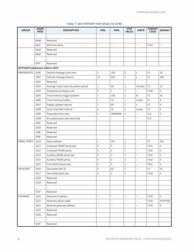
36 469 MOTOR MANAGEMENT RELAY – COMMUNICATIONS GUIDE
COMMUNICATIONS GUIDE
... ...
064B Reserved
064C Ethernet status -- -- -- -- F152 --
064D Reserved
064E Reserved
... ...
0FFF Reserved
SETPOINTS (Addresses 1000 to 1FFF)
PREFERENCES 1000 Default message cycle time 5 100 5 s F2 20
1001 Default message timeout 10 900 1 s F1 300
1002 Reserved
1003 Average motor load calculation period 1 90 1 minutes F1 15
1004 Temperature display units 0 1 1 -- F100 0
1005 Trace memory trigger position 1 100 1 % F1 25
1006 Trace memory buffers 1 16 1 cycles F1 8
1007 Display update interval 1 60 1 s F2 4
1008 Cyclic load filter interval 0 32 1 cycles F1 0
1009 Passcode (write only) 0 99999999 1 -- F12 0
100B Encrypted passcode (read only) -- -- -- -- F12 --
100C Reserved
100D Reserved
100E Reserved
100F Reserved
SERIAL PORTS 1010 Slave address 1 254 1 -- F1 254
1011 Computer RS485 baud rate 0 5 1 -- F101 4
1012 Computer RS485 parity 0 2 1 -- F102 0
1013 Auxiliary RS485 baud rate 0 5 1 -- F101 4
1014 Auxiliary RS485 parity 0 2 1 -- F102 0
1015 Front RS232 baud rate 0 5 1 -- F101 5
DEVICENET 1016 DeviceNet MAC ID 0 63 1 -- F1 32
1017 DeviceNet baud rate 0 2 1 -- F149 2
1018 Reserved
1019 Reserved
.... ...
101F Reserved
ETHERNET 1020 Ethernet IP address -- -- -- -- F150 0
1022 Ethernet subnet mask -- -- -- -- F150 FFFFFF00
1024 Ethernet gateway address -- -- -- -- F150 0
1025 Reserved
1026 Reserved
... ...
102F Reserved
Table 7: 469 MEMORY MAP (Sheet 18 of 90)
GROUP ADDR(HEX) DESCRIPTION MIN. MAX. STEP
VALUE UNITS FORMATCODE DEFAULT
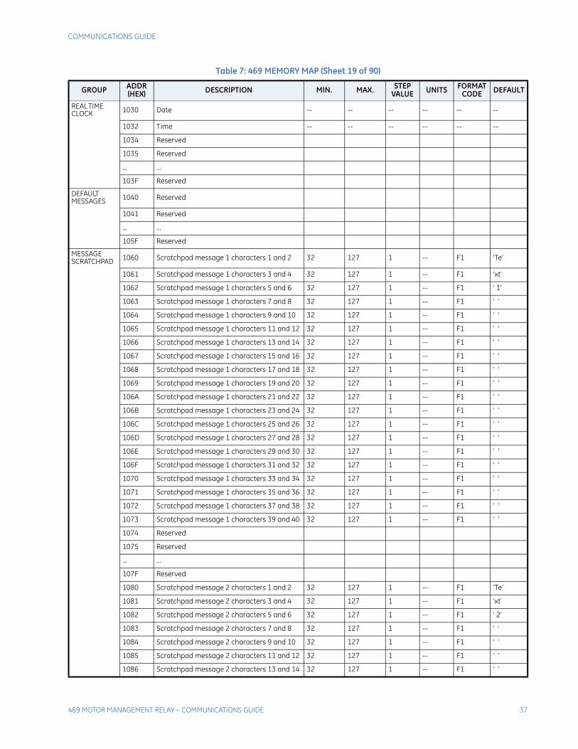
COMMUNICATIONS GUIDE
469 MOTOR MANAGEMENT RELAY – COMMUNICATIONS GUIDE 37
REAL TIME CLOCK 1030 Date -- -- -- -- -- --
1032 Time -- -- -- -- -- --
1034 Reserved
1035 Reserved
... ...
103F Reserved
DEFAULT MESSAGES 1040 Reserved
1041 Reserved
... ...
105F Reserved
MESSAGE SCRATCHPAD 1060 Scratchpad message 1 characters 1 and 2 32 127 1 -- F1 ‘Te’
1061 Scratchpad message 1 characters 3 and 4 32 127 1 -- F1 ‘xt’
1062 Scratchpad message 1 characters 5 and 6 32 127 1 -- F1 ‘ 1’
1063 Scratchpad message 1 characters 7 and 8 32 127 1 -- F1 ‘ ’
1064 Scratchpad message 1 characters 9 and 10 32 127 1 -- F1 ‘ ’
1065 Scratchpad message 1 characters 11 and 12 32 127 1 -- F1 ‘ ’
1066 Scratchpad message 1 characters 13 and 14 32 127 1 -- F1 ‘ ’
1067 Scratchpad message 1 characters 15 and 16 32 127 1 -- F1 ‘ ’
1068 Scratchpad message 1 characters 17 and 18 32 127 1 -- F1 ‘ ’
1069 Scratchpad message 1 characters 19 and 20 32 127 1 -- F1 ‘ ’
106A Scratchpad message 1 characters 21 and 22 32 127 1 -- F1 ‘ ’
106B Scratchpad message 1 characters 23 and 24 32 127 1 -- F1 ‘ ’
106C Scratchpad message 1 characters 25 and 26 32 127 1 -- F1 ‘ ’
106D Scratchpad message 1 characters 27 and 28 32 127 1 -- F1 ‘ ’
106E Scratchpad message 1 characters 29 and 30 32 127 1 -- F1 ‘ ’
106F Scratchpad message 1 characters 31 and 32 32 127 1 -- F1 ‘ ’
1070 Scratchpad message 1 characters 33 and 34 32 127 1 -- F1 ‘ ’
1071 Scratchpad message 1 characters 35 and 36 32 127 1 -- F1 ‘ ’
1072 Scratchpad message 1 characters 37 and 38 32 127 1 -- F1 ‘ ’
1073 Scratchpad message 1 characters 39 and 40 32 127 1 -- F1 ‘ ’
1074 Reserved
1075 Reserved
... ...
107F Reserved
1080 Scratchpad message 2 characters 1 and 2 32 127 1 -- F1 ‘Te’
1081 Scratchpad message 2 characters 3 and 4 32 127 1 -- F1 ‘xt’
1082 Scratchpad message 2 characters 5 and 6 32 127 1 -- F1 ‘ 2’
1083 Scratchpad message 2 characters 7 and 8 32 127 1 -- F1 ‘ ’
1084 Scratchpad message 2 characters 9 and 10 32 127 1 -- F1 ‘ ’
1085 Scratchpad message 2 characters 11 and 12 32 127 1 -- F1 ‘ ’
1086 Scratchpad message 2 characters 13 and 14 32 127 1 -- F1 ‘ ’
Table 7: 469 MEMORY MAP (Sheet 19 of 90)
GROUP ADDR(HEX) DESCRIPTION MIN. MAX. STEP
VALUE UNITS FORMATCODE DEFAULT
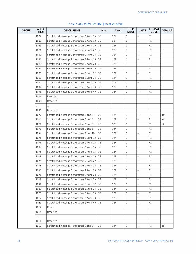
38 469 MOTOR MANAGEMENT RELAY – COMMUNICATIONS GUIDE
COMMUNICATIONS GUIDE
1087 Scratchpad message 2 characters 15 and 16 32 127 1 -- F1 ‘ ’
1088 Scratchpad message 2 characters 17 and 18 32 127 1 -- F1 ‘ ’
1089 Scratchpad message 2 characters 19 and 20 32 127 1 -- F1 ‘ ’
108A Scratchpad message 2 characters 21 and 22 32 127 1 -- F1 ‘ ’
108B Scratchpad message 2 characters 23 and 24 32 127 1 -- F1 ‘ ’
108C Scratchpad message 2 characters 25 and 26 32 127 1 -- F1 ‘ ’
108D Scratchpad message 2 characters 27 and 28 32 127 1 -- F1 ‘ ’
108E Scratchpad message 2 characters 29 and 30 32 127 1 -- F1 ‘ ’
108F Scratchpad message 2 characters 31 and 32 32 127 1 -- F1 ‘ ’
1090 Scratchpad message 2 characters 33 and 34 32 127 1 -- F1 ‘ ’
1091 Scratchpad message 2 characters 35 and 36 32 127 1 -- F1 ‘ ’
1092 Scratchpad message 2 characters 37 and 38 32 127 1 -- F1 ‘ ’
1093 Scratchpad message 2 characters 39 and 40 32 127 1 -- F1 ‘ ’
1094 Reserved
1095 Reserved
... ...
109F Reserved
10A0 Scratchpad message 3 characters 1 and 2 32 127 1 -- F1 ‘Te’
10A1 Scratchpad message 3 characters 3 and 4 32 127 1 -- F1 ‘xt’
10A2 Scratchpad message 3 characters 5 and 6 32 127 1 -- F1 ‘ 3’
10A3 Scratchpad message 3 characters 7 and 8 32 127 1 -- F1 ‘ ’
10A4 Scratchpad message 3 characters 9 and 10 32 127 1 -- F1 ‘ ’
10A5 Scratchpad message 3 characters 11 and 12 32 127 1 -- F1 ‘ ’
10A6 Scratchpad message 3 characters 13 and 14 32 127 1 -- F1 ‘ ’
10A7 Scratchpad message 3 characters 15 and 16 32 127 1 -- F1 ‘ ’
10A8 Scratchpad message 3 characters 17 and 18 32 127 1 -- F1 ‘ ’
10A9 Scratchpad message 3 characters 19 and 20 32 127 1 -- F1 ‘ ’
10AA Scratchpad message 3 characters 21 and 22 32 127 1 -- F1 ‘ ’
10AB Scratchpad message 3 characters 23 and 24 32 127 1 -- F1 ‘ ’
10AC Scratchpad message 3 characters 25 and 26 32 127 1 -- F1 ‘ ’
10AD Scratchpad message 3 characters 27 and 28 32 127 1 -- F1 ‘ ’
10AE Scratchpad message 3 characters 29 and 30 32 127 1 -- F1 ‘ ’
10AF Scratchpad message 3 characters 31 and 32 32 127 1 -- F1 ‘ ’
10B0 Scratchpad message 3 characters 33 and 34 32 127 1 -- F1 ‘ ’
10B1 Scratchpad message 3 characters 35 and 36 32 127 1 -- F1 ‘ ’
10B2 Scratchpad message 3 characters 37 and 38 32 127 1 -- F1 ‘ ’
10B3 Scratchpad message 3 characters 39 and 40 32 127 1 -- F1 ‘ ’
10B4 Reserved
10B5 Reserved
... ...
10BF Reserved
10C0 Scratchpad message 4 characters 1 and 2 32 127 1 -- F1 ‘Te’
Table 7: 469 MEMORY MAP (Sheet 20 of 90)
GROUP ADDR(HEX) DESCRIPTION MIN. MAX. STEP
VALUE UNITS FORMATCODE DEFAULT
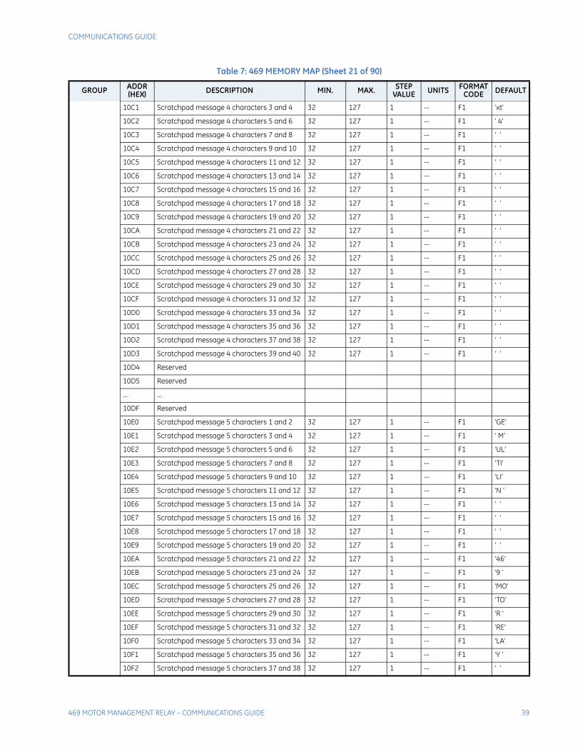
COMMUNICATIONS GUIDE
469 MOTOR MANAGEMENT RELAY – COMMUNICATIONS GUIDE 39
10C1 Scratchpad message 4 characters 3 and 4 32 127 1 -- F1 ‘xt’
10C2 Scratchpad message 4 characters 5 and 6 32 127 1 -- F1 ‘ 4’
10C3 Scratchpad message 4 characters 7 and 8 32 127 1 -- F1 ‘ ’
10C4 Scratchpad message 4 characters 9 and 10 32 127 1 -- F1 ‘ ’
10C5 Scratchpad message 4 characters 11 and 12 32 127 1 -- F1 ‘ ’
10C6 Scratchpad message 4 characters 13 and 14 32 127 1 -- F1 ‘ ’
10C7 Scratchpad message 4 characters 15 and 16 32 127 1 -- F1 ‘ ’
10C8 Scratchpad message 4 characters 17 and 18 32 127 1 -- F1 ‘ ’
10C9 Scratchpad message 4 characters 19 and 20 32 127 1 -- F1 ‘ ’
10CA Scratchpad message 4 characters 21 and 22 32 127 1 -- F1 ‘ ’
10CB Scratchpad message 4 characters 23 and 24 32 127 1 -- F1 ‘ ’
10CC Scratchpad message 4 characters 25 and 26 32 127 1 -- F1 ‘ ’
10CD Scratchpad message 4 characters 27 and 28 32 127 1 -- F1 ‘ ’
10CE Scratchpad message 4 characters 29 and 30 32 127 1 -- F1 ‘ ’
10CF Scratchpad message 4 characters 31 and 32 32 127 1 -- F1 ‘ ’
10D0 Scratchpad message 4 characters 33 and 34 32 127 1 -- F1 ‘ ’
10D1 Scratchpad message 4 characters 35 and 36 32 127 1 -- F1 ‘ ’
10D2 Scratchpad message 4 characters 37 and 38 32 127 1 -- F1 ‘ ’
10D3 Scratchpad message 4 characters 39 and 40 32 127 1 -- F1 ‘ ’
10D4 Reserved
10D5 Reserved
... ...
10DF Reserved
10E0 Scratchpad message 5 characters 1 and 2 32 127 1 -- F1 ‘GE’
10E1 Scratchpad message 5 characters 3 and 4 32 127 1 -- F1 ‘ M’
10E2 Scratchpad message 5 characters 5 and 6 32 127 1 -- F1 ‘UL’
10E3 Scratchpad message 5 characters 7 and 8 32 127 1 -- F1 ‘TI’
10E4 Scratchpad message 5 characters 9 and 10 32 127 1 -- F1 ‘LI’
10E5 Scratchpad message 5 characters 11 and 12 32 127 1 -- F1 ‘N ’
10E6 Scratchpad message 5 characters 13 and 14 32 127 1 -- F1 ‘ ’
10E7 Scratchpad message 5 characters 15 and 16 32 127 1 -- F1 ‘ ’
10E8 Scratchpad message 5 characters 17 and 18 32 127 1 -- F1 ‘ ’
10E9 Scratchpad message 5 characters 19 and 20 32 127 1 -- F1 ‘ ’
10EA Scratchpad message 5 characters 21 and 22 32 127 1 -- F1 ‘46’
10EB Scratchpad message 5 characters 23 and 24 32 127 1 -- F1 ‘9 ’
10EC Scratchpad message 5 characters 25 and 26 32 127 1 -- F1 ‘MO’
10ED Scratchpad message 5 characters 27 and 28 32 127 1 -- F1 ‘TO’
10EE Scratchpad message 5 characters 29 and 30 32 127 1 -- F1 ‘R ’
10EF Scratchpad message 5 characters 31 and 32 32 127 1 -- F1 ‘RE’
10F0 Scratchpad message 5 characters 33 and 34 32 127 1 -- F1 ‘LA’
10F1 Scratchpad message 5 characters 35 and 36 32 127 1 -- F1 ‘Y ’
10F2 Scratchpad message 5 characters 37 and 38 32 127 1 -- F1 ‘ ’
Table 7: 469 MEMORY MAP (Sheet 21 of 90)
GROUP ADDR(HEX) DESCRIPTION MIN. MAX. STEP
VALUE UNITS FORMATCODE DEFAULT
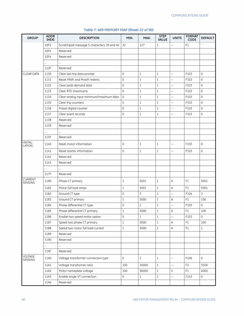
40 469 MOTOR MANAGEMENT RELAY – COMMUNICATIONS GUIDE
COMMUNICATIONS GUIDE
10F3 Scratchpad message 5 characters 39 and 40 32 127 1 -- F1 ‘ ’
10F4 Reserved
10F4 Reserved
... ...
112F Reserved
CLEAR DATA 1130 Clear last trip data prompt 0 1 1 -- F103 0
1131 Reset MWh and Mvarh meters 0 1 1 -- F103 0
1132 Clear peak demand data 0 1 1 -- F103 0
1133 Clear RTD maximums 0 1 1 -- F103 0
1134 Clear analog input minimum/maximum data 0 1 1 -- F103 0
1135 Clear trip counters 0 1 1 -- F103 0
1136 Preset digital counter 0 1 1 -- F103 0
1137 Clear event records 0 1 1 -- F103 0
1138 Reserved
1139 Reserved
... ...
113F Reserved
INSTAL-LATION 1140 Reset motor information 0 1 1 -- F103 0
1141 Reset starter information 0 1 1 -- F103 0
1142 Reserved
1143 Reserved
... ...
117F Reserved
CURRENT SENSING 1180 Phase CT primary 1 5001 1 A F1 5001
1181 Motor full load amps 1 5001 1 A F1 5001
1182 Ground CT type 0 3 1 -- F104 3
1183 Ground CT primary 1 5000 1 A F1 100
1184 Phase differential CT type 0 2 1 -- F105 0
1185 Phase differential CT primary 1 5000 1 A F1 100
1186 Enable two speed motor option 0 1 1 -- F103 0
1187 Speed two phase CT primary 1 5000 1 A F1 100
1188 Speed two motor full load current 1 5000 1 A F1 1
1189 Reserved
1190 Reserved
... ...
119F Reserved
VOLTAGE SENSING 11A0 Voltage transformer connection type 0 2 1 -- F106 0
11A1 Voltage transformer ratio 100 30000 1 -- F3 3500
11A2 Motor nameplate voltage 100 36000 1 V F1 4000
11A3 Enable single VT connection 0 1 1 -- F143 0
11A4 Reserved
Table 7: 469 MEMORY MAP (Sheet 22 of 90)
GROUP ADDR(HEX) DESCRIPTION MIN. MAX. STEP
VALUE UNITS FORMATCODE DEFAULT
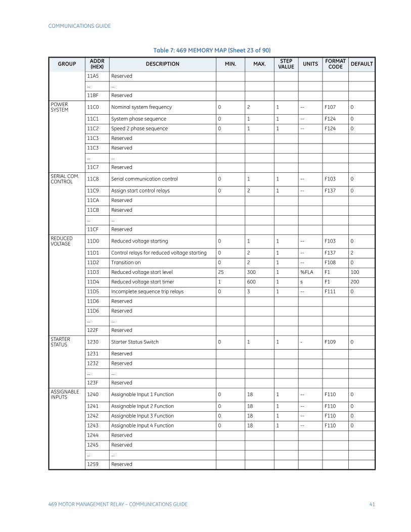
COMMUNICATIONS GUIDE
469 MOTOR MANAGEMENT RELAY – COMMUNICATIONS GUIDE 41
11A5 Reserved
... ...
11BF Reserved
POWERSYSTEM 11C0 Nominal system frequency 0 2 1 -- F107 0
11C1 System phase sequence 0 1 1 -- F124 0
11C2 Speed 2 phase sequence 0 1 1 -- F124 0
11C3 Reserved
11C3 Reserved
... ...
11C7 Reserved
SERIAL COM.CONTROL 11C8 Serial communication control 0 1 1 -- F103 0
11C9 Assign start control relays 0 2 1 -- F137 0
11CA Reserved
11CB Reserved
... ...
11CF Reserved
REDUCED VOLTAGE 11D0 Reduced voltage starting 0 1 1 -- F103 0
11D1 Control relays for reduced voltage starting 0 2 1 -- F137 2
11D2 Transition on 0 2 1 -- F108 0
11D3 Reduced voltage start level 25 300 1 %FLA F1 100
11D4 Reduced voltage start timer 1 600 1 s F1 200
11D5 Incomplete sequence trip relays 0 3 1 -- F111 0
11D6 Reserved
11D6 Reserved
... ...
122F Reserved
STARTER STATUS 1230 Starter Status Switch 0 1 1 - F109 0
1231 Reserved
1232 Reserved
... ...
123F Reserved
ASSIGNABLE INPUTS 1240 Assignable Input 1 Function 0 18 1 -- F110 0
1241 Assignable Input 2 Function 0 18 1 -- F110 0
1242 Assignable Input 3 Function 0 18 1 -- F110 0
1243 Assignable Input 4 Function 0 18 1 -- F110 0
1244 Reserved
1245 Reserved
... ...
1259 Reserved
Table 7: 469 MEMORY MAP (Sheet 23 of 90)
GROUP ADDR(HEX) DESCRIPTION MIN. MAX. STEP
VALUE UNITS FORMATCODE DEFAULT
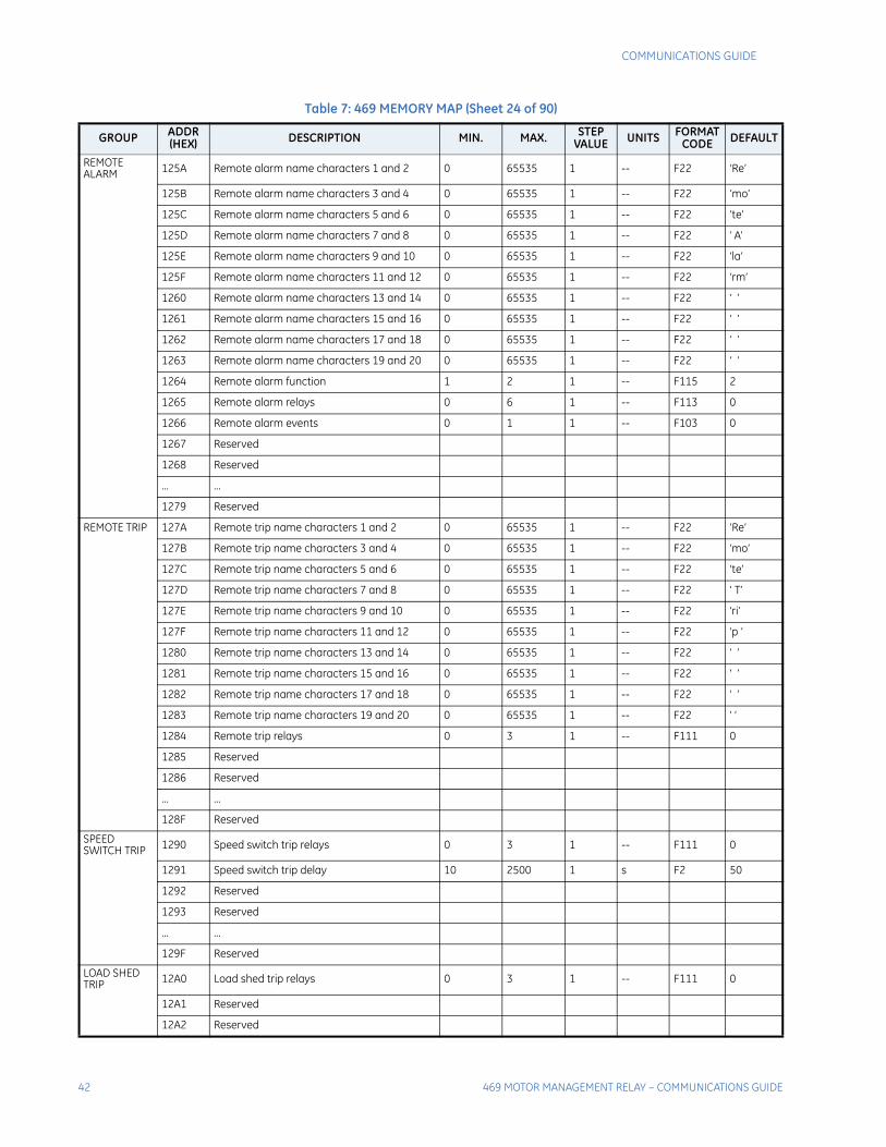
42 469 MOTOR MANAGEMENT RELAY – COMMUNICATIONS GUIDE
COMMUNICATIONS GUIDE
REMOTE ALARM 125A Remote alarm name characters 1 and 2 0 65535 1 -- F22 ‘Re’
125B Remote alarm name characters 3 and 4 0 65535 1 -- F22 ‘mo’
125C Remote alarm name characters 5 and 6 0 65535 1 -- F22 ‘te’
125D Remote alarm name characters 7 and 8 0 65535 1 -- F22 ‘ A’
125E Remote alarm name characters 9 and 10 0 65535 1 -- F22 ‘la’
125F Remote alarm name characters 11 and 12 0 65535 1 -- F22 ‘rm’
1260 Remote alarm name characters 13 and 14 0 65535 1 -- F22 ‘ ’
1261 Remote alarm name characters 15 and 16 0 65535 1 -- F22 ‘ ’
1262 Remote alarm name characters 17 and 18 0 65535 1 -- F22 ‘ ’
1263 Remote alarm name characters 19 and 20 0 65535 1 -- F22 ‘ ’
1264 Remote alarm function 1 2 1 -- F115 2
1265 Remote alarm relays 0 6 1 -- F113 0
1266 Remote alarm events 0 1 1 -- F103 0
1267 Reserved
1268 Reserved
... ...
1279 Reserved
REMOTE TRIP 127A Remote trip name characters 1 and 2 0 65535 1 -- F22 ‘Re’
127B Remote trip name characters 3 and 4 0 65535 1 -- F22 ‘mo’
127C Remote trip name characters 5 and 6 0 65535 1 -- F22 ‘te’
127D Remote trip name characters 7 and 8 0 65535 1 -- F22 ‘ T’
127E Remote trip name characters 9 and 10 0 65535 1 -- F22 ‘ri’
127F Remote trip name characters 11 and 12 0 65535 1 -- F22 ‘p ’
1280 Remote trip name characters 13 and 14 0 65535 1 -- F22 ‘ ’
1281 Remote trip name characters 15 and 16 0 65535 1 -- F22 ‘ ’
1282 Remote trip name characters 17 and 18 0 65535 1 -- F22 ‘ ’
1283 Remote trip name characters 19 and 20 0 65535 1 -- F22 ‘ ’
1284 Remote trip relays 0 3 1 -- F111 0
1285 Reserved
1286 Reserved
... ...
128F Reserved
SPEED SWITCH TRIP 1290 Speed switch trip relays 0 3 1 -- F111 0
1291 Speed switch trip delay 10 2500 1 s F2 50
1292 Reserved
1293 Reserved
... ...
129F Reserved
LOAD SHED TRIP 12A0 Load shed trip relays 0 3 1 -- F111 0
12A1 Reserved
12A2 Reserved
Table 7: 469 MEMORY MAP (Sheet 24 of 90)
GROUP ADDR(HEX) DESCRIPTION MIN. MAX. STEP
VALUE UNITS FORMATCODE DEFAULT
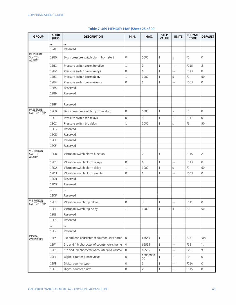
COMMUNICATIONS GUIDE
469 MOTOR MANAGEMENT RELAY – COMMUNICATIONS GUIDE 43
... ...
12AF Reserved
PRESSURE SWITCH ALARM
12B0 Block pressure switch alarm from start 0 5000 1 s F1 0
12B1 Pressure switch alarm function 1 2 1 -- F115 2
12B2 Pressure switch alarm relays 0 6 1 -- F113 0
12B3 Pressure switch alarm delay 1 1000 1 s F2 50
12B4 Pressure switch alarm events 0 1 1 -- F103 0
12B5 Reserved
12B6 Reserved
... ...
12BF Reserved
PRESSURE SWITCH TRIP 12C0 Block pressure switch trip from start 0 5000 1 s F1 0
12C1 Pressure switch trip relays 0 3 1 -- F111 0
12C2 Pressure switch trip delay 1 1000 1 s F2 50
12C3 Reserved
12CD Reserved
12CE Reserved
12CF Reserved
VIBRATION SWITCH ALARM
12D0 Vibration switch alarm function 1 2 1 -- F115 2
12D1 Vibration switch alarm relays 0 6 1 -- F113 0
12D2 Vibration switch alarm delay 1 1000 1 s F2 50
12D3 Vibration switch alarm events 0 1 1 -- F103 0
12D4 Reserved
12D5 Reserved
... ...
12DF Reserved
VIBRATION SWITCH TRIP 12E0 Vibration switch trip relays 0 3 1 -- F111 0
12E1 Vibration switch trip delay 1 1000 1 s F2 50
12E2 Reserved
12E3 Reserved
... ...
12F2 Reserved
DIGITAL COUNTERS 12F3 1st and 2nd character of counter units name 0 65535 1 -- F22 ‘Un’
12F4 3rd and 4th character of counter units name 0 65535 1 -- F22 ‘it’
12F5 5th and 6th character of counter units name 0 65535 1 -- F22 ‘s ’
12F6 Digital counter preset value 0 1000000000 1 -- F9 0
12F8 Digital counter type 0 1 1 -- F114 0
12F9 Digital counter alarm 0 2 1 -- F115 0
Table 7: 469 MEMORY MAP (Sheet 25 of 90)
GROUP ADDR(HEX) DESCRIPTION MIN. MAX. STEP
VALUE UNITS FORMATCODE DEFAULT
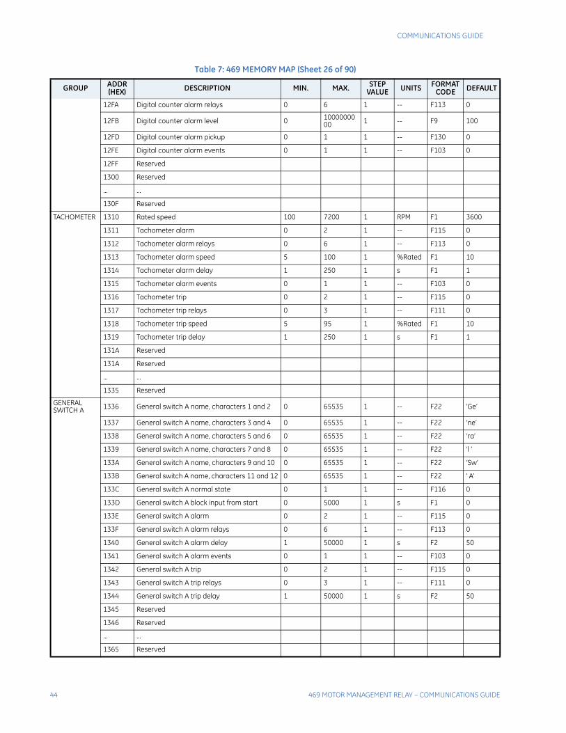
44 469 MOTOR MANAGEMENT RELAY – COMMUNICATIONS GUIDE
COMMUNICATIONS GUIDE
12FA Digital counter alarm relays 0 6 1 -- F113 0
12FB Digital counter alarm level 0 1000000000 1 -- F9 100
12FD Digital counter alarm pickup 0 1 1 -- F130 0
12FE Digital counter alarm events 0 1 1 -- F103 0
12FF Reserved
1300 Reserved
... ...
130F Reserved
TACHOMETER 1310 Rated speed 100 7200 1 RPM F1 3600
1311 Tachometer alarm 0 2 1 -- F115 0
1312 Tachometer alarm relays 0 6 1 -- F113 0
1313 Tachometer alarm speed 5 100 1 %Rated F1 10
1314 Tachometer alarm delay 1 250 1 s F1 1
1315 Tachometer alarm events 0 1 1 -- F103 0
1316 Tachometer trip 0 2 1 -- F115 0
1317 Tachometer trip relays 0 3 1 -- F111 0
1318 Tachometer trip speed 5 95 1 %Rated F1 10
1319 Tachometer trip delay 1 250 1 s F1 1
131A Reserved
131A Reserved
... ...
1335 Reserved
GENERAL SWITCH A 1336 General switch A name, characters 1 and 2 0 65535 1 -- F22 ‘Ge’
1337 General switch A name, characters 3 and 4 0 65535 1 -- F22 ‘ne’
1338 General switch A name, characters 5 and 6 0 65535 1 -- F22 ‘ra’
1339 General switch A name, characters 7 and 8 0 65535 1 -- F22 ‘l ’
133A General switch A name, characters 9 and 10 0 65535 1 -- F22 ‘Sw’
133B General switch A name, characters 11 and 12 0 65535 1 -- F22 ‘ A’
133C General switch A normal state 0 1 1 -- F116 0
133D General switch A block input from start 0 5000 1 s F1 0
133E General switch A alarm 0 2 1 -- F115 0
133F General switch A alarm relays 0 6 1 -- F113 0
1340 General switch A alarm delay 1 50000 1 s F2 50
1341 General switch A alarm events 0 1 1 -- F103 0
1342 General switch A trip 0 2 1 -- F115 0
1343 General switch A trip relays 0 3 1 -- F111 0
1344 General switch A trip delay 1 50000 1 s F2 50
1345 Reserved
1346 Reserved
... ...
1365 Reserved
Table 7: 469 MEMORY MAP (Sheet 26 of 90)
GROUP ADDR(HEX) DESCRIPTION MIN. MAX. STEP
VALUE UNITS FORMATCODE DEFAULT
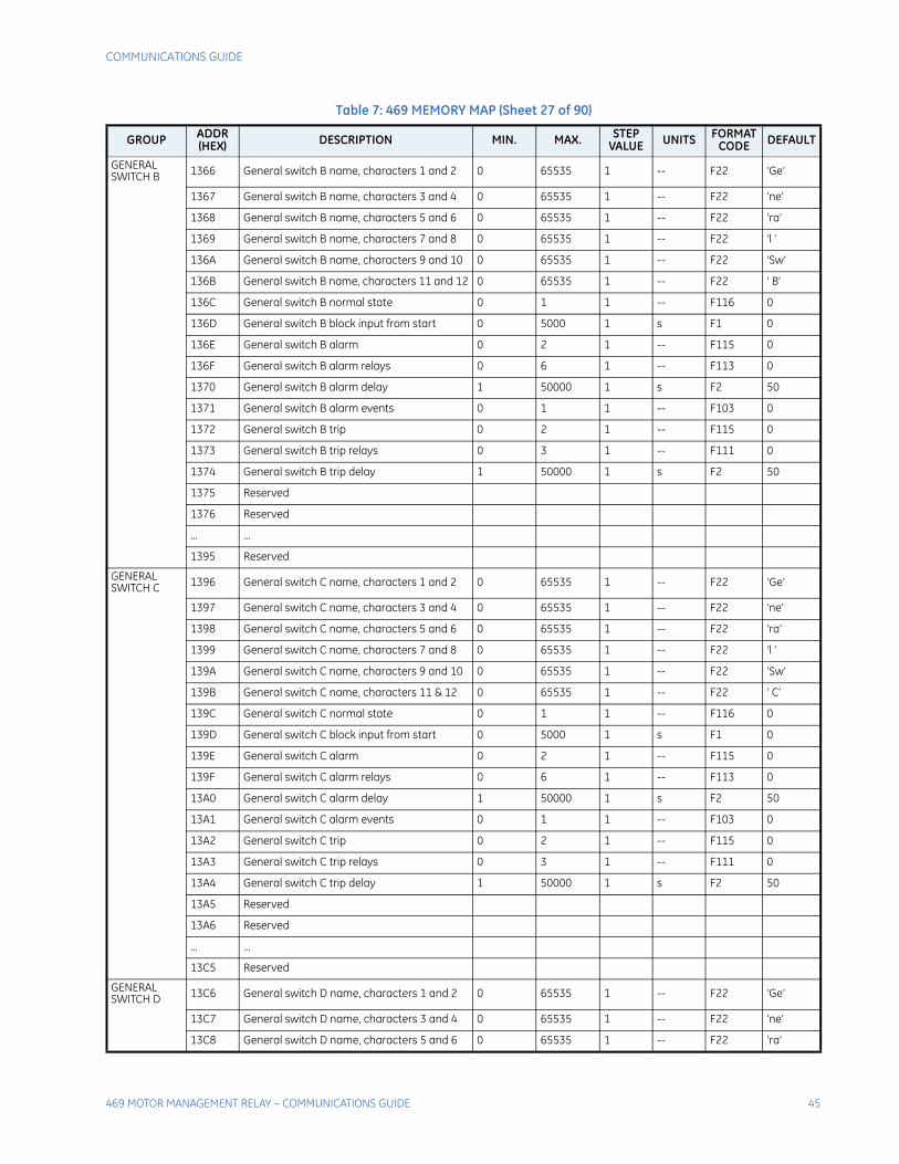
COMMUNICATIONS GUIDE
469 MOTOR MANAGEMENT RELAY – COMMUNICATIONS GUIDE 45
GENERAL SWITCH B 1366 General switch B name, characters 1 and 2 0 65535 1 -- F22 ‘Ge’
1367 General switch B name, characters 3 and 4 0 65535 1 -- F22 ‘ne’
1368 General switch B name, characters 5 and 6 0 65535 1 -- F22 ‘ra’
1369 General switch B name, characters 7 and 8 0 65535 1 -- F22 ‘l ’
136A General switch B name, characters 9 and 10 0 65535 1 -- F22 ‘Sw’
136B General switch B name, characters 11 and 12 0 65535 1 -- F22 ‘ B’
136C General switch B normal state 0 1 1 -- F116 0
136D General switch B block input from start 0 5000 1 s F1 0
136E General switch B alarm 0 2 1 -- F115 0
136F General switch B alarm relays 0 6 1 -- F113 0
1370 General switch B alarm delay 1 50000 1 s F2 50
1371 General switch B alarm events 0 1 1 -- F103 0
1372 General switch B trip 0 2 1 -- F115 0
1373 General switch B trip relays 0 3 1 -- F111 0
1374 General switch B trip delay 1 50000 1 s F2 50
1375 Reserved
1376 Reserved
... ...
1395 Reserved
GENERAL SWITCH C 1396 General switch C name, characters 1 and 2 0 65535 1 -- F22 ‘Ge’
1397 General switch C name, characters 3 and 4 0 65535 1 -- F22 ‘ne’
1398 General switch C name, characters 5 and 6 0 65535 1 -- F22 ‘ra’
1399 General switch C name, characters 7 and 8 0 65535 1 -- F22 ‘l ’
139A General switch C name, characters 9 and 10 0 65535 1 -- F22 ‘Sw’
139B General switch C name, characters 11 & 12 0 65535 1 -- F22 ‘ C’
139C General switch C normal state 0 1 1 -- F116 0
139D General switch C block input from start 0 5000 1 s F1 0
139E General switch C alarm 0 2 1 -- F115 0
139F General switch C alarm relays 0 6 1 -- F113 0
13A0 General switch C alarm delay 1 50000 1 s F2 50
13A1 General switch C alarm events 0 1 1 -- F103 0
13A2 General switch C trip 0 2 1 -- F115 0
13A3 General switch C trip relays 0 3 1 -- F111 0
13A4 General switch C trip delay 1 50000 1 s F2 50
13A5 Reserved
13A6 Reserved
... ...
13C5 Reserved
GENERAL SWITCH D 13C6 General switch D name, characters 1 and 2 0 65535 1 -- F22 ‘Ge’
13C7 General switch D name, characters 3 and 4 0 65535 1 -- F22 ‘ne’
13C8 General switch D name, characters 5 and 6 0 65535 1 -- F22 ‘ra’
Table 7: 469 MEMORY MAP (Sheet 27 of 90)
GROUP ADDR(HEX) DESCRIPTION MIN. MAX. STEP
VALUE UNITS FORMATCODE DEFAULT
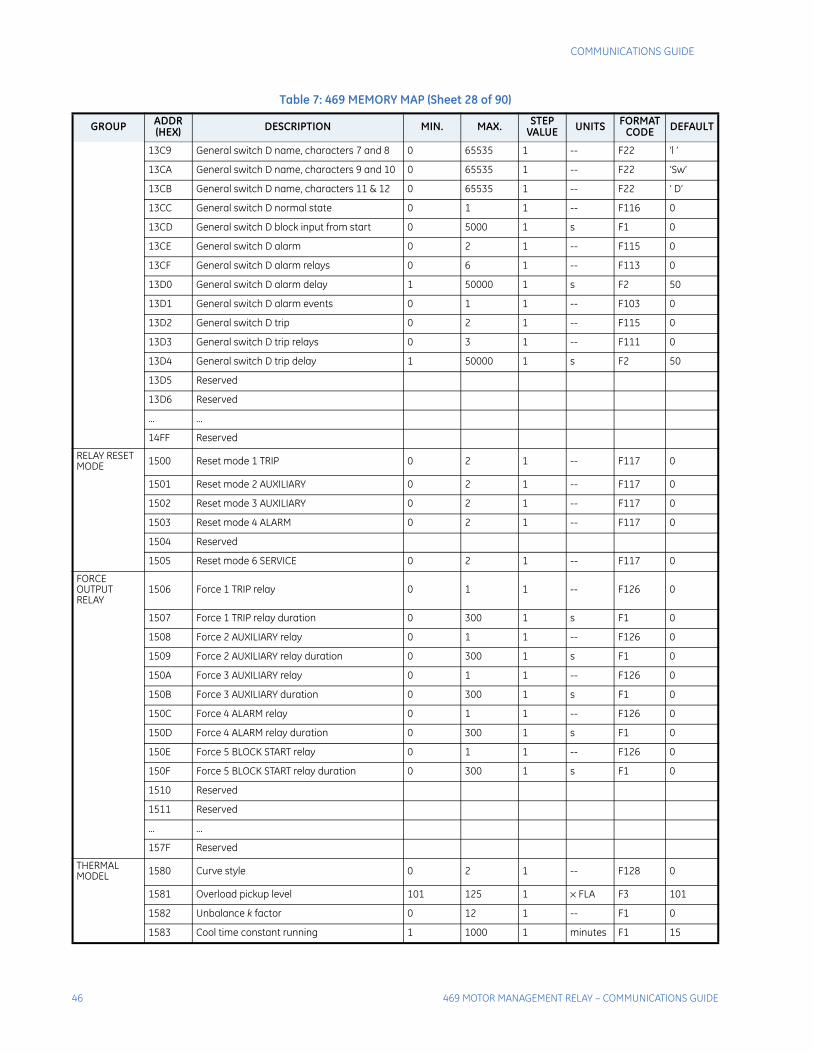
46 469 MOTOR MANAGEMENT RELAY – COMMUNICATIONS GUIDE
COMMUNICATIONS GUIDE
13C9 General switch D name, characters 7 and 8 0 65535 1 -- F22 ‘l ’
13CA General switch D name, characters 9 and 10 0 65535 1 -- F22 ‘Sw’
13CB General switch D name, characters 11 & 12 0 65535 1 -- F22 ‘ D’
13CC General switch D normal state 0 1 1 -- F116 0
13CD General switch D block input from start 0 5000 1 s F1 0
13CE General switch D alarm 0 2 1 -- F115 0
13CF General switch D alarm relays 0 6 1 -- F113 0
13D0 General switch D alarm delay 1 50000 1 s F2 50
13D1 General switch D alarm events 0 1 1 -- F103 0
13D2 General switch D trip 0 2 1 -- F115 0
13D3 General switch D trip relays 0 3 1 -- F111 0
13D4 General switch D trip delay 1 50000 1 s F2 50
13D5 Reserved
13D6 Reserved
... ...
14FF Reserved
RELAY RESET MODE 1500 Reset mode 1 TRIP 0 2 1 -- F117 0
1501 Reset mode 2 AUXILIARY 0 2 1 -- F117 0
1502 Reset mode 3 AUXILIARY 0 2 1 -- F117 0
1503 Reset mode 4 ALARM 0 2 1 -- F117 0
1504 Reserved
1505 Reset mode 6 SERVICE 0 2 1 -- F117 0
FORCEOUTPUT RELAY
1506 Force 1 TRIP relay 0 1 1 -- F126 0
1507 Force 1 TRIP relay duration 0 300 1 s F1 0
1508 Force 2 AUXILIARY relay 0 1 1 -- F126 0
1509 Force 2 AUXILIARY relay duration 0 300 1 s F1 0
150A Force 3 AUXILIARY relay 0 1 1 -- F126 0
150B Force 3 AUXILIARY duration 0 300 1 s F1 0
150C Force 4 ALARM relay 0 1 1 -- F126 0
150D Force 4 ALARM relay duration 0 300 1 s F1 0
150E Force 5 BLOCK START relay 0 1 1 -- F126 0
150F Force 5 BLOCK START relay duration 0 300 1 s F1 0
1510 Reserved
1511 Reserved
... ...
157F Reserved
THERMAL MODEL 1580 Curve style 0 2 1 -- F128 0
1581 Overload pickup level 101 125 1 × FLA F3 101
1582 Unbalance k factor 0 12 1 -- F1 0
1583 Cool time constant running 1 1000 1 minutes F1 15
Table 7: 469 MEMORY MAP (Sheet 28 of 90)
GROUP ADDR(HEX) DESCRIPTION MIN. MAX. STEP
VALUE UNITS FORMATCODE DEFAULT
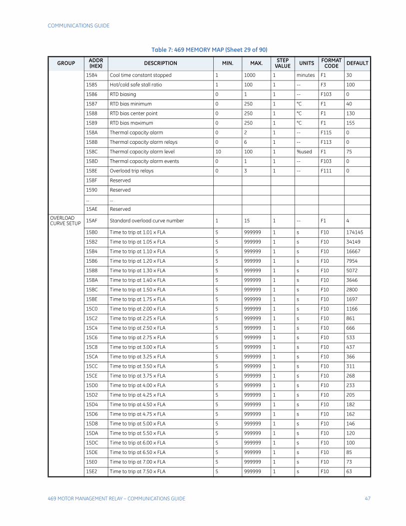
COMMUNICATIONS GUIDE
469 MOTOR MANAGEMENT RELAY – COMMUNICATIONS GUIDE 47
1584 Cool time constant stopped 1 1000 1 minutes F1 30
1585 Hot/cold safe stall ratio 1 100 1 -- F3 100
1586 RTD biasing 0 1 1 -- F103 0
1587 RTD bias minimum 0 250 1 °C F1 40
1588 RTD bias center point 0 250 1 °C F1 130
1589 RTD bias maximum 0 250 1 °C F1 155
158A Thermal capacity alarm 0 2 1 -- F115 0
158B Thermal capacity alarm relays 0 6 1 -- F113 0
158C Thermal capacity alarm level 10 100 1 %used F1 75
158D Thermal capacity alarm events 0 1 1 -- F103 0
158E Overload trip relays 0 3 1 -- F111 0
158F Reserved
1590 Reserved
... ...
15AE Reserved
OVERLOAD CURVE SETUP 15AF Standard overload curve number 1 15 1 -- F1 4
15B0 Time to trip at 1.01 x FLA 5 999999 1 s F10 174145
15B2 Time to trip at 1.05 x FLA 5 999999 1 s F10 34149
15B4 Time to trip at 1.10 x FLA 5 999999 1 s F10 16667
15B6 Time to trip at 1.20 x FLA 5 999999 1 s F10 7954
15B8 Time to trip at 1.30 x FLA 5 999999 1 s F10 5072
15BA Time to trip at 1.40 x FLA 5 999999 1 s F10 3646
15BC Time to trip at 1.50 x FLA 5 999999 1 s F10 2800
15BE Time to trip at 1.75 x FLA 5 999999 1 s F10 1697
15C0 Time to trip at 2.00 x FLA 5 999999 1 s F10 1166
15C2 Time to trip at 2.25 x FLA 5 999999 1 s F10 861
15C4 Time to trip at 2.50 x FLA 5 999999 1 s F10 666
15C6 Time to trip at 2.75 x FLA 5 999999 1 s F10 533
15C8 Time to trip at 3.00 x FLA 5 999999 1 s F10 437
15CA Time to trip at 3.25 x FLA 5 999999 1 s F10 366
15CC Time to trip at 3.50 x FLA 5 999999 1 s F10 311
15CE Time to trip at 3.75 x FLA 5 999999 1 s F10 268
15D0 Time to trip at 4.00 x FLA 5 999999 1 s F10 233
15D2 Time to trip at 4.25 x FLA 5 999999 1 s F10 205
15D4 Time to trip at 4.50 x FLA 5 999999 1 s F10 182
15D6 Time to trip at 4.75 x FLA 5 999999 1 s F10 162
15D8 Time to trip at 5.00 x FLA 5 999999 1 s F10 146
15DA Time to trip at 5.50 x FLA 5 999999 1 s F10 120
15DC Time to trip at 6.00 x FLA 5 999999 1 s F10 100
15DE Time to trip at 6.50 x FLA 5 999999 1 s F10 85
15E0 Time to trip at 7.00 x FLA 5 999999 1 s F10 73
15E2 Time to trip at 7.50 x FLA 5 999999 1 s F10 63
Table 7: 469 MEMORY MAP (Sheet 29 of 90)
GROUP ADDR(HEX) DESCRIPTION MIN. MAX. STEP
VALUE UNITS FORMATCODE DEFAULT
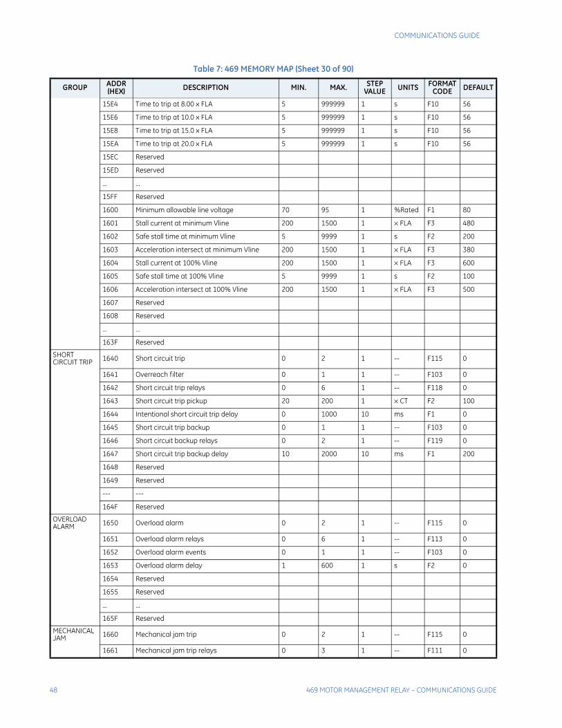
48 469 MOTOR MANAGEMENT RELAY – COMMUNICATIONS GUIDE
COMMUNICATIONS GUIDE
15E4 Time to trip at 8.00 x FLA 5 999999 1 s F10 56
15E6 Time to trip at 10.0 x FLA 5 999999 1 s F10 56
15E8 Time to trip at 15.0 x FLA 5 999999 1 s F10 56
15EA Time to trip at 20.0 x FLA 5 999999 1 s F10 56
15EC Reserved
15ED Reserved
... ...
15FF Reserved
1600 Minimum allowable line voltage 70 95 1 %Rated F1 80
1601 Stall current at minimum Vline 200 1500 1 × FLA F3 480
1602 Safe stall time at minimum Vline 5 9999 1 s F2 200
1603 Acceleration intersect at minimum Vline 200 1500 1 × FLA F3 380
1604 Stall current at 100% Vline 200 1500 1 × FLA F3 600
1605 Safe stall time at 100% Vline 5 9999 1 s F2 100
1606 Acceleration intersect at 100% Vline 200 1500 1 × FLA F3 500
1607 Reserved
1608 Reserved
… …
163F Reserved
SHORTCIRCUIT TRIP 1640 Short circuit trip 0 2 1 -- F115 0
1641 Overreach filter 0 1 1 -- F103 0
1642 Short circuit trip relays 0 6 1 -- F118 0
1643 Short circuit trip pickup 20 200 1 × CT F2 100
1644 Intentional short circuit trip delay 0 1000 10 ms F1 0
1645 Short circuit trip backup 0 1 1 -- F103 0
1646 Short circuit backup relays 0 2 1 -- F119 0
1647 Short circuit trip backup delay 10 2000 10 ms F1 200
1648 Reserved
1649 Reserved
--- ---
164F Reserved
OVERLOAD ALARM 1650 Overload alarm 0 2 1 -- F115 0
1651 Overload alarm relays 0 6 1 -- F113 0
1652 Overload alarm events 0 1 1 -- F103 0
1653 Overload alarm delay 1 600 1 s F2 0
1654 Reserved
1655 Reserved
... ...
165F Reserved
MECHANICALJAM 1660 Mechanical jam trip 0 2 1 -- F115 0
1661 Mechanical jam trip relays 0 3 1 -- F111 0
Table 7: 469 MEMORY MAP (Sheet 30 of 90)
GROUP ADDR(HEX) DESCRIPTION MIN. MAX. STEP
VALUE UNITS FORMATCODE DEFAULT
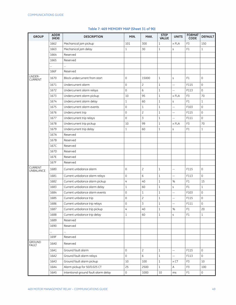
COMMUNICATIONS GUIDE
469 MOTOR MANAGEMENT RELAY – COMMUNICATIONS GUIDE 49
1662 Mechanical jam pickup 101 300 1 × FLA F3 150
1663 Mechanical jam delay 1 30 1 s F1 1
1664 Reserved
1665 Reserved
... ...
166F Reserved
UNDER-CURRENT 1670 Block undercurrent from start 0 15000 1 s F1 0
1671 Undercurrent alarm 0 2 1 -- F115 0
1672 Undercurrent alarm relays 0 6 1 -- F113 0
1673 Undercurrent alarm pickup 10 95 1 × FLA F3 70
1674 Undercurrent alarm delay 1 60 1 s F1 1
1675 Undercurrent alarm events 0 1 1 -- F103 0
1676 Undercurrent trip 0 2 1 -- F115 0
1677 Undercurrent trip relays 0 3 1 -- F111 0
1678 Undercurrent trip pickup 10 99 1 × FLA F3 70
1679 Undercurrent trip delay 1 60 1 s F1 1
167A Reserved
167B Reserved
167C Reserved
167D Reserved
167E Reserved
167F Reserved
CURRENT UNBALANCE 1680 Current unbalance alarm 0 2 1 -- F115 0
1681 Current unbalance alarm relays 0 6 1 -- F113 0
1682 Current unbalance alarm pickup 4 40 1 % F1 15
1683 Current unbalance alarm delay 1 60 1 s F1 1
1684 Current unbalance alarm events 0 1 1 -- F103 0
1685 Current unbalance trip 0 2 1 -- F115 0
1686 Current unbalance trip relays 0 3 1 -- F111 0
1687 Current unbalance trip pickup 4 40 1 % F1 20
1688 Current unbalance trip delay 1 60 1 s F1 1
1689 Reserved
1690 Reserved
... ...
169F Reserved
GROUND FAULT 16A0 Reserved
16A1 Ground fault alarm 0 2 1 -- F115 0
16A2 Ground fault alarm relays 0 6 1 -- F113 0
16A3 Ground fault alarm pickup 10 100 1 × CT F3 10
16A4 Alarm pickup for 50/0.025 CT 25 2500 1 A F3 100
16A5 Intentional ground fault alarm delay 0 1000 10 ms F1 0
Table 7: 469 MEMORY MAP (Sheet 31 of 90)
GROUP ADDR(HEX) DESCRIPTION MIN. MAX. STEP
VALUE UNITS FORMATCODE DEFAULT
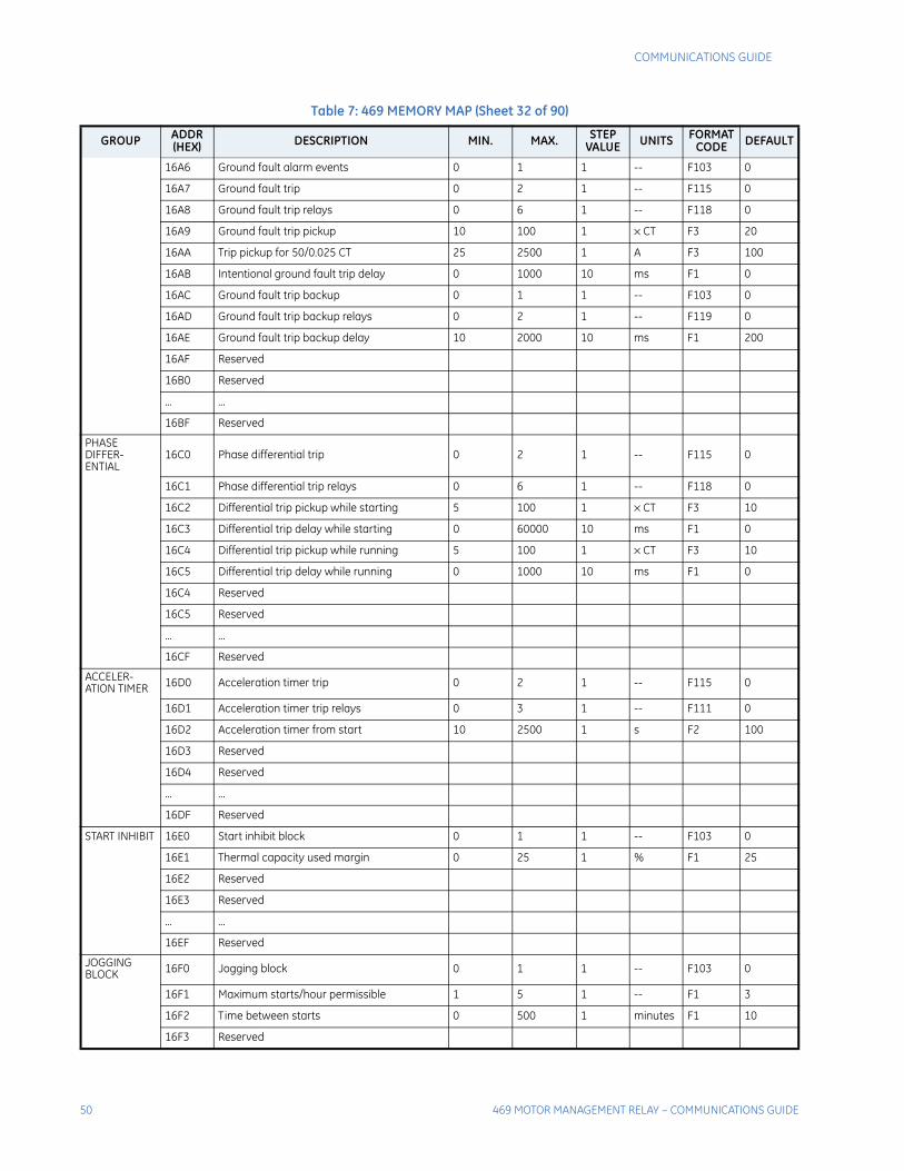
50 469 MOTOR MANAGEMENT RELAY – COMMUNICATIONS GUIDE
COMMUNICATIONS GUIDE
16A6 Ground fault alarm events 0 1 1 -- F103 0
16A7 Ground fault trip 0 2 1 -- F115 0
16A8 Ground fault trip relays 0 6 1 -- F118 0
16A9 Ground fault trip pickup 10 100 1 × CT F3 20
16AA Trip pickup for 50/0.025 CT 25 2500 1 A F3 100
16AB Intentional ground fault trip delay 0 1000 10 ms F1 0
16AC Ground fault trip backup 0 1 1 -- F103 0
16AD Ground fault trip backup relays 0 2 1 -- F119 0
16AE Ground fault trip backup delay 10 2000 10 ms F1 200
16AF Reserved
16B0 Reserved
... ...
16BF Reserved
PHASEDIFFER-ENTIAL
16C0 Phase differential trip 0 2 1 -- F115 0
16C1 Phase differential trip relays 0 6 1 -- F118 0
16C2 Differential trip pickup while starting 5 100 1 × CT F3 10
16C3 Differential trip delay while starting 0 60000 10 ms F1 0
16C4 Differential trip pickup while running 5 100 1 × CT F3 10
16C5 Differential trip delay while running 0 1000 10 ms F1 0
16C4 Reserved
16C5 Reserved
... ...
16CF Reserved
ACCELER-ATION TIMER 16D0 Acceleration timer trip 0 2 1 -- F115 0
16D1 Acceleration timer trip relays 0 3 1 -- F111 0
16D2 Acceleration timer from start 10 2500 1 s F2 100
16D3 Reserved
16D4 Reserved
... ...
16DF Reserved
START INHIBIT 16E0 Start inhibit block 0 1 1 -- F103 0
16E1 Thermal capacity used margin 0 25 1 % F1 25
16E2 Reserved
16E3 Reserved
... ...
16EF Reserved
JOGGING BLOCK 16F0 Jogging block 0 1 1 -- F103 0
16F1 Maximum starts/hour permissible 1 5 1 -- F1 3
16F2 Time between starts 0 500 1 minutes F1 10
16F3 Reserved
Table 7: 469 MEMORY MAP (Sheet 32 of 90)
GROUP ADDR(HEX) DESCRIPTION MIN. MAX. STEP
VALUE UNITS FORMATCODE DEFAULT
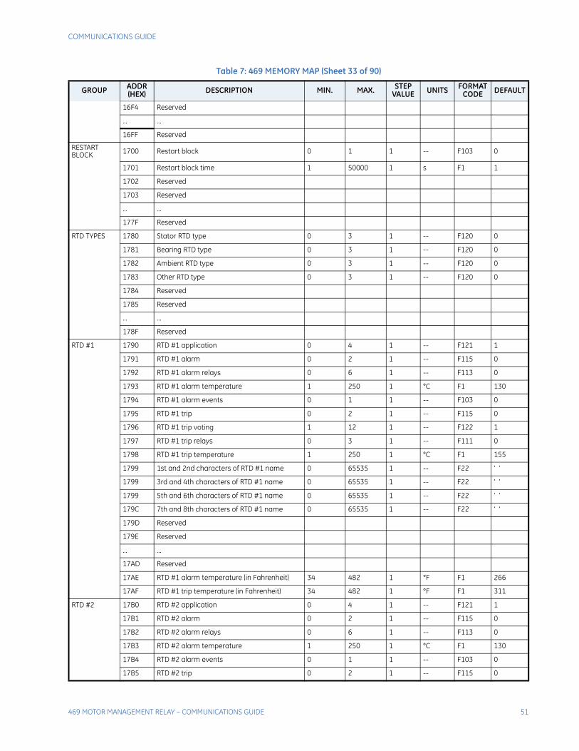
COMMUNICATIONS GUIDE
469 MOTOR MANAGEMENT RELAY – COMMUNICATIONS GUIDE 51
16F4 Reserved
... ...
16FF Reserved
RESTART BLOCK 1700 Restart block 0 1 1 -- F103 0
1701 Restart block time 1 50000 1 s F1 1
1702 Reserved
1703 Reserved
... ...
177F Reserved
RTD TYPES 1780 Stator RTD type 0 3 1 -- F120 0
1781 Bearing RTD type 0 3 1 -- F120 0
1782 Ambient RTD type 0 3 1 -- F120 0
1783 Other RTD type 0 3 1 -- F120 0
1784 Reserved
1785 Reserved
... ...
178F Reserved
RTD #1 1790 RTD #1 application 0 4 1 -- F121 1
1791 RTD #1 alarm 0 2 1 -- F115 0
1792 RTD #1 alarm relays 0 6 1 -- F113 0
1793 RTD #1 alarm temperature 1 250 1 °C F1 130
1794 RTD #1 alarm events 0 1 1 -- F103 0
1795 RTD #1 trip 0 2 1 -- F115 0
1796 RTD #1 trip voting 1 12 1 -- F122 1
1797 RTD #1 trip relays 0 3 1 -- F111 0
1798 RTD #1 trip temperature 1 250 1 °C F1 155
1799 1st and 2nd characters of RTD #1 name 0 65535 1 -- F22 ‘ ’
1799 3rd and 4th characters of RTD #1 name 0 65535 1 -- F22 ‘ ’
1799 5th and 6th characters of RTD #1 name 0 65535 1 -- F22 ‘ ’
179C 7th and 8th characters of RTD #1 name 0 65535 1 -- F22 ‘ ’
179D Reserved
179E Reserved
... ...
17AD Reserved
17AE RTD #1 alarm temperature (in Fahrenheit) 34 482 1 °F F1 266
17AF RTD #1 trip temperature (in Fahrenheit) 34 482 1 °F F1 311
RTD #2 17B0 RTD #2 application 0 4 1 -- F121 1
17B1 RTD #2 alarm 0 2 1 -- F115 0
17B2 RTD #2 alarm relays 0 6 1 -- F113 0
17B3 RTD #2 alarm temperature 1 250 1 °C F1 130
17B4 RTD #2 alarm events 0 1 1 -- F103 0
17B5 RTD #2 trip 0 2 1 -- F115 0
Table 7: 469 MEMORY MAP (Sheet 33 of 90)
GROUP ADDR(HEX) DESCRIPTION MIN. MAX. STEP
VALUE UNITS FORMATCODE DEFAULT
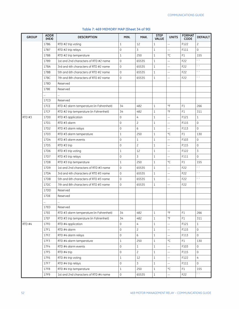
52 469 MOTOR MANAGEMENT RELAY – COMMUNICATIONS GUIDE
COMMUNICATIONS GUIDE
17B6 RTD #2 trip voting 1 12 1 -- F122 2
17B7 RTD #2 trip relays 0 3 1 -- F111 0
17B8 RTD #2 trip temperature 1 250 1 °C F1 155
17B9 1st and 2nd characters of RTD #2 name 0 65535 1 -- F22 ‘ ’
17BA 3rd and 4th characters of RTD #2 name 0 65535 1 -- F22 ‘ ’
17BB 5th and 6th characters of RTD #2 name 0 65535 1 -- F22 ‘ ’
17BC 7th and 8th characters of RTD #2 name 0 65535 1 -- F22 ‘ ’
17BD Reserved
17BE Reserved
... ...
17CD Reserved
17CE RTD #2 alarm temperature (in Fahrenheit) 34 482 1 °F F1 266
17CF RTD #2 trip temperature (in Fahrenheit) 34 482 1 °F F1 311
RTD #3 17D0 RTD #3 application 0 4 1 -- F121 1
17D1 RTD #3 alarm 0 2 1 -- F115 0
17D2 RTD #3 alarm relays 0 6 1 -- F113 0
17D3 RTD #3 alarm temperature 1 250 1 °C F1 130
17D4 RTD #3 alarm events 0 1 1 -- F103 0
17D5 RTD #3 trip 0 2 1 -- F115 0
17D6 RTD #3 trip voting 1 12 1 -- F122 3
17D7 RTD #3 trip relays 0 3 1 -- F111 0
17D8 RTD #3 trip temperature 1 250 1 °C F1 155
17D9 1st and 2nd characters of RTD #3 name 0 65535 1 -- F22 ‘ ’
17DA 3rd and 4th characters of RTD #3 name 0 65535 1 -- F22 ‘ ’
17DB 5th and 6th characters of RTD #3 name 0 65535 1 -- F22 ‘ ’
17DC 7th and 8th characters of RTD #3 name 0 65535 1 -- F22 ‘ ’
17DD Reserved
17DE Reserved
... ...
17ED Reserved
17EE RTD #3 alarm temperature (in Fahrenheit) 34 482 1 °F F1 266
17EF RTD #3 trip temperature (in Fahrenheit) 34 482 1 °F F1 311
RTD #4 17F0 RTD #4 application 0 4 1 -- F121 1
17F1 RTD #4 alarm 0 2 1 -- F115 0
17F2 RTD #4 alarm relays 0 6 1 -- F113 0
17F3 RTD #4 alarm temperature 1 250 1 °C F1 130
17F4 RTD #4 alarm events 0 1 1 -- F103 0
17F5 RTD #4 trip 0 2 1 -- F115 0
17F6 RTD #4 trip voting 1 12 1 -- F122 4
17F7 RTD #4 trip relays 0 3 1 -- F111 0
17F8 RTD #4 trip temperature 1 250 1 °C F1 155
17F9 1st and 2nd characters of RTD #4 name 0 65535 1 -- F22 ‘ ’
Table 7: 469 MEMORY MAP (Sheet 34 of 90)
GROUP ADDR(HEX) DESCRIPTION MIN. MAX. STEP
VALUE UNITS FORMATCODE DEFAULT
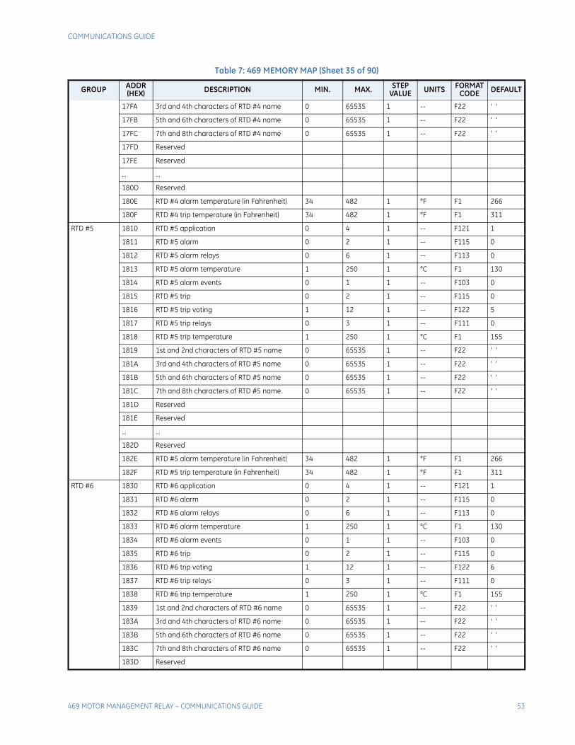
COMMUNICATIONS GUIDE
469 MOTOR MANAGEMENT RELAY – COMMUNICATIONS GUIDE 53
17FA 3rd and 4th characters of RTD #4 name 0 65535 1 -- F22 ‘ ’
17FB 5th and 6th characters of RTD #4 name 0 65535 1 -- F22 ‘ ’
17FC 7th and 8th characters of RTD #4 name 0 65535 1 -- F22 ‘ ’
17FD Reserved
17FE Reserved
... ...
180D Reserved
180E RTD #4 alarm temperature (in Fahrenheit) 34 482 1 °F F1 266
180F RTD #4 trip temperature (in Fahrenheit) 34 482 1 °F F1 311
RTD #5 1810 RTD #5 application 0 4 1 -- F121 1
1811 RTD #5 alarm 0 2 1 -- F115 0
1812 RTD #5 alarm relays 0 6 1 -- F113 0
1813 RTD #5 alarm temperature 1 250 1 °C F1 130
1814 RTD #5 alarm events 0 1 1 -- F103 0
1815 RTD #5 trip 0 2 1 -- F115 0
1816 RTD #5 trip voting 1 12 1 -- F122 5
1817 RTD #5 trip relays 0 3 1 -- F111 0
1818 RTD #5 trip temperature 1 250 1 °C F1 155
1819 1st and 2nd characters of RTD #5 name 0 65535 1 -- F22 ‘ ’
181A 3rd and 4th characters of RTD #5 name 0 65535 1 -- F22 ‘ ’
181B 5th and 6th characters of RTD #5 name 0 65535 1 -- F22 ‘ ’
181C 7th and 8th characters of RTD #5 name 0 65535 1 -- F22 ‘ ’
181D Reserved
181E Reserved
... ...
182D Reserved
182E RTD #5 alarm temperature (in Fahrenheit) 34 482 1 °F F1 266
182F RTD #5 trip temperature (in Fahrenheit) 34 482 1 °F F1 311
RTD #6 1830 RTD #6 application 0 4 1 -- F121 1
1831 RTD #6 alarm 0 2 1 -- F115 0
1832 RTD #6 alarm relays 0 6 1 -- F113 0
1833 RTD #6 alarm temperature 1 250 1 °C F1 130
1834 RTD #6 alarm events 0 1 1 -- F103 0
1835 RTD #6 trip 0 2 1 -- F115 0
1836 RTD #6 trip voting 1 12 1 -- F122 6
1837 RTD #6 trip relays 0 3 1 -- F111 0
1838 RTD #6 trip temperature 1 250 1 °C F1 155
1839 1st and 2nd characters of RTD #6 name 0 65535 1 -- F22 ‘ ’
183A 3rd and 4th characters of RTD #6 name 0 65535 1 -- F22 ‘ ’
183B 5th and 6th characters of RTD #6 name 0 65535 1 -- F22 ‘ ’
183C 7th and 8th characters of RTD #6 name 0 65535 1 -- F22 ‘ ’
183D Reserved
Table 7: 469 MEMORY MAP (Sheet 35 of 90)
GROUP ADDR(HEX) DESCRIPTION MIN. MAX. STEP
VALUE UNITS FORMATCODE DEFAULT
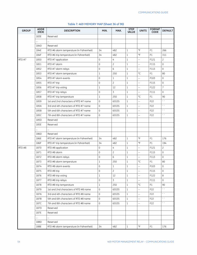
54 469 MOTOR MANAGEMENT RELAY – COMMUNICATIONS GUIDE
COMMUNICATIONS GUIDE
183E Reserved
... ...
184D Reserved
184E RTD #6 alarm temperature (in Fahrenheit) 34 482 1 °F F1 266
184F RTD #6 trip temperature (in Fahrenheit) 34 482 1 °F F1 311
RTD #7 1850 RTD #7 application 0 4 1 -- F121 2
1851 RTD #7 alarm 0 2 1 -- F115 0
1852 RTD #7 alarm relays 0 6 1 -- F113 0
1853 RTD #7 alarm temperature 1 250 1 °C F1 80
1854 RTD #7 alarm events 0 1 1 -- F103 0
1855 RTD #7 trip 0 2 1 -- F115 0
1856 RTD #7 trip voting 1 12 1 -- F122 7
1857 RTD #7 trip relays 0 3 1 -- F111 0
1858 RTD #7 trip temperature 1 250 1 °C F1 90
1859 1st and 2nd characters of RTD #7 name 0 65535 1 -- F22 ‘ ’
185A 3rd and 4th characters of RTD #7 name 0 65535 1 -- F22 ‘ ’
185B 5th and 6th characters of RTD #7 name 0 65535 1 -- F22 ‘ ’
185C 7th and 8th characters of RTD #7 name 0 65535 1 -- F22 ‘ ’
185D Reserved
185E Reserved
... ...
186D Reserved
186E RTD #7 alarm temperature (in Fahrenheit) 34 482 1 °F F1 176
186F RTD #7 trip temperature (in Fahrenheit) 34 482 1 °F F1 194
RTD #8 1870 RTD #8 application 0 4 1 -- F121 2
1871 RTD #8 alarm 0 2 1 -- F115 0
1872 RTD #8 alarm relays 0 6 1 -- F113 0
1873 RTD #8 alarm temperature 1 250 1 °C F1 80
1874 RTD #8 alarm events 0 1 1 -- F103 0
1875 RTD #8 trip 0 2 1 -- F115 0
1876 RTD #8 trip voting 1 12 1 -- F122 8
1877 RTD #8 trip relays 0 3 1 -- F111 0
1878 RTD #8 trip temperature 1 250 1 °C F1 90
1879 1st and 2nd characters of RTD #8 name 0 65535 1 -- F22 ‘ ’
187A 3rd and 4th characters of RTD #8 name 0 65535 1 -- F22 ‘ ’
187B 5th and 6th characters of RTD #8 name 0 65535 1 -- F22 ‘ ’
187C 7th and 8th characters of RTD #8 name 0 65535 1 -- F22 ‘ ’
187D Reserved
187E Reserved
... ...
188D Reserved
188E RTD #8 alarm temperature (in Fahrenheit) 34 482 1 °F F1 176
Table 7: 469 MEMORY MAP (Sheet 36 of 90)
GROUP ADDR(HEX) DESCRIPTION MIN. MAX. STEP
VALUE UNITS FORMATCODE DEFAULT
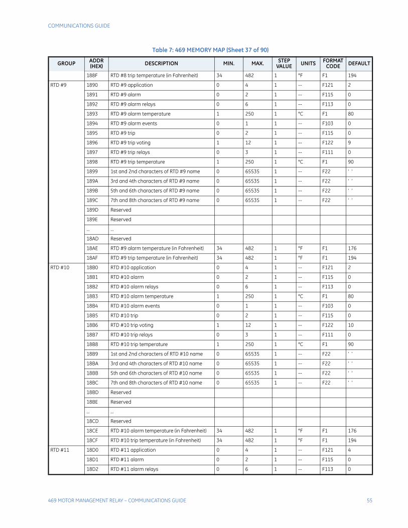
COMMUNICATIONS GUIDE
469 MOTOR MANAGEMENT RELAY – COMMUNICATIONS GUIDE 55
188F RTD #8 trip temperature (in Fahrenheit) 34 482 1 °F F1 194
RTD #9 1890 RTD #9 application 0 4 1 -- F121 2
1891 RTD #9 alarm 0 2 1 -- F115 0
1892 RTD #9 alarm relays 0 6 1 -- F113 0
1893 RTD #9 alarm temperature 1 250 1 °C F1 80
1894 RTD #9 alarm events 0 1 1 -- F103 0
1895 RTD #9 trip 0 2 1 -- F115 0
1896 RTD #9 trip voting 1 12 1 -- F122 9
1897 RTD #9 trip relays 0 3 1 -- F111 0
1898 RTD #9 trip temperature 1 250 1 °C F1 90
1899 1st and 2nd characters of RTD #9 name 0 65535 1 -- F22 ‘ ’
189A 3rd and 4th characters of RTD #9 name 0 65535 1 -- F22 ‘ ’
189B 5th and 6th characters of RTD #9 name 0 65535 1 -- F22 ‘ ’
189C 7th and 8th characters of RTD #9 name 0 65535 1 -- F22 ‘ ’
189D Reserved
189E Reserved
... ...
18AD Reserved
18AE RTD #9 alarm temperature (in Fahrenheit) 34 482 1 °F F1 176
18AF RTD #9 trip temperature (in Fahrenheit) 34 482 1 °F F1 194
RTD #10 18B0 RTD #10 application 0 4 1 -- F121 2
18B1 RTD #10 alarm 0 2 1 -- F115 0
18B2 RTD #10 alarm relays 0 6 1 -- F113 0
18B3 RTD #10 alarm temperature 1 250 1 °C F1 80
18B4 RTD #10 alarm events 0 1 1 -- F103 0
18B5 RTD #10 trip 0 2 1 -- F115 0
18B6 RTD #10 trip voting 1 12 1 -- F122 10
18B7 RTD #10 trip relays 0 3 1 -- F111 0
18B8 RTD #10 trip temperature 1 250 1 °C F1 90
18B9 1st and 2nd characters of RTD #10 name 0 65535 1 -- F22 ‘ ’
18BA 3rd and 4th characters of RTD #10 name 0 65535 1 -- F22 ‘ ’
18BB 5th and 6th characters of RTD #10 name 0 65535 1 -- F22 ‘ ’
18BC 7th and 8th characters of RTD #10 name 0 65535 1 -- F22 ‘ ’
18BD Reserved
18BE Reserved
... ...
18CD Reserved
18CE RTD #10 alarm temperature (in Fahrenheit) 34 482 1 °F F1 176
18CF RTD #10 trip temperature (in Fahrenheit) 34 482 1 °F F1 194
RTD #11 18D0 RTD #11 application 0 4 1 -- F121 4
18D1 RTD #11 alarm 0 2 1 -- F115 0
18D2 RTD #11 alarm relays 0 6 1 -- F113 0
Table 7: 469 MEMORY MAP (Sheet 37 of 90)
GROUP ADDR(HEX) DESCRIPTION MIN. MAX. STEP
VALUE UNITS FORMATCODE DEFAULT
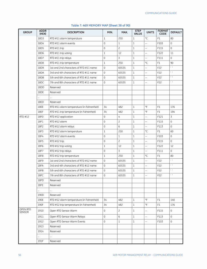
56 469 MOTOR MANAGEMENT RELAY – COMMUNICATIONS GUIDE
COMMUNICATIONS GUIDE
18D3 RTD #11 alarm temperature 1 250 1 °C F1 80
18D4 RTD #11 alarm events 0 1 1 -- F103 0
18D5 RTD #11 trip 0 2 1 -- F115 0
18D6 RTD #11 trip voting 1 12 1 -- F122 11
18D7 RTD #11 trip relays 0 3 1 -- F111 0
18D8 RTD #11 trip temperature 1 250 1 °C F1 90
18D9 1st and 2nd characters of RTD #11 name 0 65535 1 -- F22 ‘ ’
18DA 3rd and 4th characters of RTD #11 name 0 65535 1 -- F22 ‘ ’
18DB 5th and 6th characters of RTD #11 name 0 65535 1 -- F22 ‘ ’
18DC 7th and 8th characters of RTD #11 name 0 65535 1 -- F22 ‘ ’
18DD Reserved
18DE Reserved
... ...
18ED Reserved
18EE RTD #11 alarm temperature (in Fahrenheit) 34 482 1 °F F1 176
18EF RTD #11 trip temperature (in Fahrenheit) 34 482 1 °F F1 194
RTD #12 18F0 RTD #12 application 0 4 1 -- F121 3
18F1 RTD #12 alarm 0 2 1 -- F115 0
18F2 RTD #12 alarm relays 0 6 1 -- F113 0
18F3 RTD #12 alarm temperature 1 250 1 °C F1 60
18F4 RTD #12 alarm events 0 1 1 -- F103 0
18F5 RTD #12 trip 0 2 1 -- F115 0
18F6 RTD #12 trip voting 1 12 1 -- F122 12
18F7 RTD #12 trip relays 0 3 1 -- F111 0
18F8 RTD #12 trip temperature 1 250 1 °C F1 80
18F9 1st and 2nd characters of RTD #12 name 0 65535 1 -- F22 ‘ ’
18FA 3rd and 4th characters of RTD #12 name 0 65535 1 -- F22 ‘ ’
18FB 5th and 6th characters of RTD #12 name 0 65535 1 -- F22 ‘ ’
18FC 7th and 8th characters of RTD #12 name 0 65535 1 -- F22 ‘ ’
18FD Reserved
18FE Reserved
... ...
190D Reserved
190E RTD #12 alarm temperature (in Fahrenheit) 34 482 1 °F F1 140
190F RTD #12 trip temperature (in Fahrenheit) 34 482 1 °F F1 176
OPEN RTD SENSOR 1910 Open RTD Sensor Alarm 0 2 1 -- F115 0
1911 Open RTD Sensor Alarm Relays 0 6 1 -- F113 0
1912 Open RTD Sensor Alarm Events 0 1 1 -- F103 0
1913 Reserved
1914 Reserved
... ...
191F Reserved
Table 7: 469 MEMORY MAP (Sheet 38 of 90)
GROUP ADDR(HEX) DESCRIPTION MIN. MAX. STEP
VALUE UNITS FORMATCODE DEFAULT
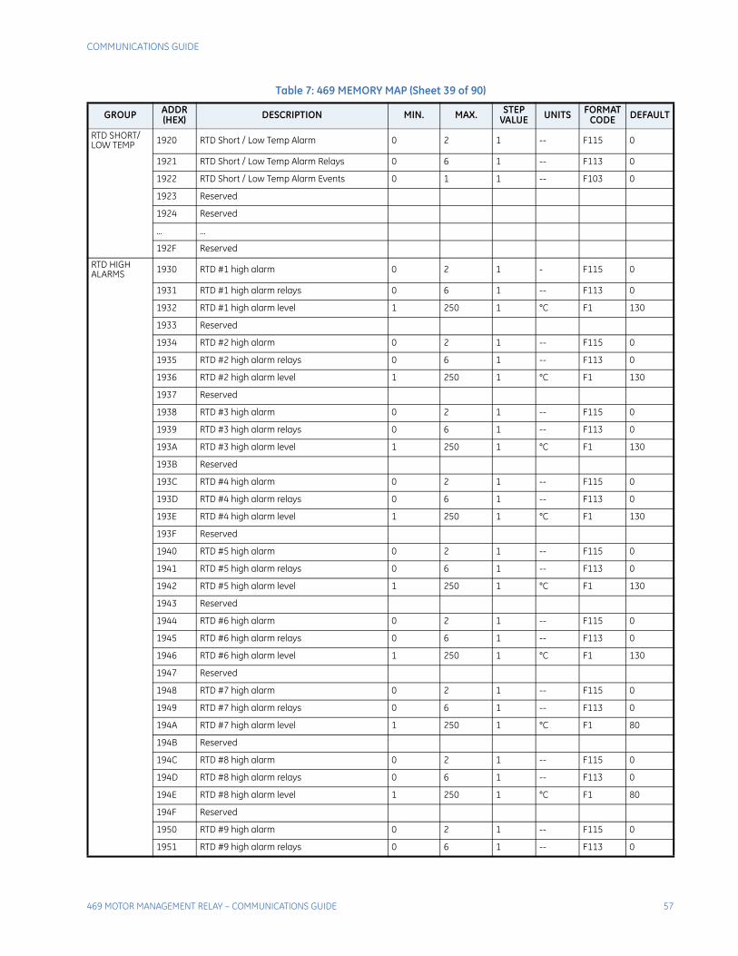
COMMUNICATIONS GUIDE
469 MOTOR MANAGEMENT RELAY – COMMUNICATIONS GUIDE 57
RTD SHORT/LOW TEMP 1920 RTD Short / Low Temp Alarm 0 2 1 -- F115 0
1921 RTD Short / Low Temp Alarm Relays 0 6 1 -- F113 0
1922 RTD Short / Low Temp Alarm Events 0 1 1 -- F103 0
1923 Reserved
1924 Reserved
... ...
192F Reserved
RTD HIGH ALARMS 1930 RTD #1 high alarm 0 2 1 - F115 0
1931 RTD #1 high alarm relays 0 6 1 -- F113 0
1932 RTD #1 high alarm level 1 250 1 °C F1 130
1933 Reserved
1934 RTD #2 high alarm 0 2 1 -- F115 0
1935 RTD #2 high alarm relays 0 6 1 -- F113 0
1936 RTD #2 high alarm level 1 250 1 °C F1 130
1937 Reserved
1938 RTD #3 high alarm 0 2 1 -- F115 0
1939 RTD #3 high alarm relays 0 6 1 -- F113 0
193A RTD #3 high alarm level 1 250 1 °C F1 130
193B Reserved
193C RTD #4 high alarm 0 2 1 -- F115 0
193D RTD #4 high alarm relays 0 6 1 -- F113 0
193E RTD #4 high alarm level 1 250 1 °C F1 130
193F Reserved
1940 RTD #5 high alarm 0 2 1 -- F115 0
1941 RTD #5 high alarm relays 0 6 1 -- F113 0
1942 RTD #5 high alarm level 1 250 1 °C F1 130
1943 Reserved
1944 RTD #6 high alarm 0 2 1 -- F115 0
1945 RTD #6 high alarm relays 0 6 1 -- F113 0
1946 RTD #6 high alarm level 1 250 1 °C F1 130
1947 Reserved
1948 RTD #7 high alarm 0 2 1 -- F115 0
1949 RTD #7 high alarm relays 0 6 1 -- F113 0
194A RTD #7 high alarm level 1 250 1 °C F1 80
194B Reserved
194C RTD #8 high alarm 0 2 1 -- F115 0
194D RTD #8 high alarm relays 0 6 1 -- F113 0
194E RTD #8 high alarm level 1 250 1 °C F1 80
194F Reserved
1950 RTD #9 high alarm 0 2 1 -- F115 0
1951 RTD #9 high alarm relays 0 6 1 -- F113 0
Table 7: 469 MEMORY MAP (Sheet 39 of 90)
GROUP ADDR(HEX) DESCRIPTION MIN. MAX. STEP
VALUE UNITS FORMATCODE DEFAULT
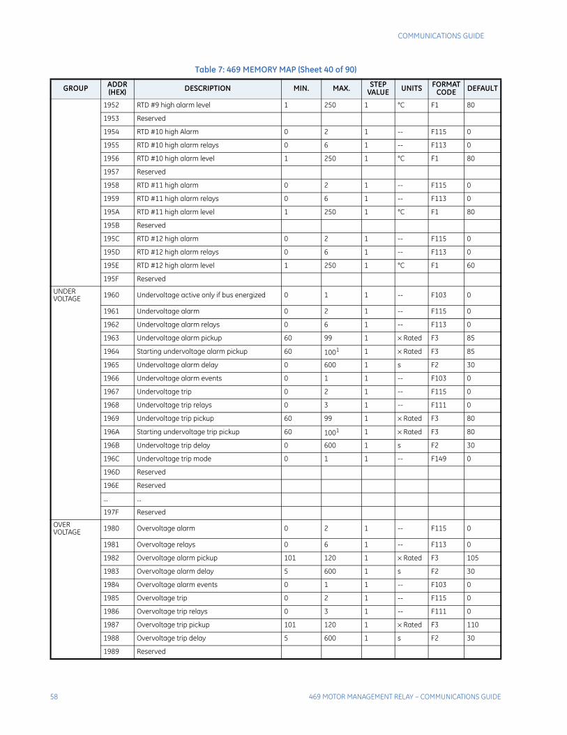
58 469 MOTOR MANAGEMENT RELAY – COMMUNICATIONS GUIDE
COMMUNICATIONS GUIDE
1952 RTD #9 high alarm level 1 250 1 °C F1 80
1953 Reserved
1954 RTD #10 high Alarm 0 2 1 -- F115 0
1955 RTD #10 high alarm relays 0 6 1 -- F113 0
1956 RTD #10 high alarm level 1 250 1 °C F1 80
1957 Reserved
1958 RTD #11 high alarm 0 2 1 -- F115 0
1959 RTD #11 high alarm relays 0 6 1 -- F113 0
195A RTD #11 high alarm level 1 250 1 °C F1 80
195B Reserved
195C RTD #12 high alarm 0 2 1 -- F115 0
195D RTD #12 high alarm relays 0 6 1 -- F113 0
195E RTD #12 high alarm level 1 250 1 °C F1 60
195F Reserved
UNDERVOLTAGE 1960 Undervoltage active only if bus energized 0 1 1 -- F103 0
1961 Undervoltage alarm 0 2 1 -- F115 0
1962 Undervoltage alarm relays 0 6 1 -- F113 0
1963 Undervoltage alarm pickup 60 99 1 × Rated F3 85
1964 Starting undervoltage alarm pickup 60 1001 1 × Rated F3 85
1965 Undervoltage alarm delay 0 600 1 s F2 30
1966 Undervoltage alarm events 0 1 1 -- F103 0
1967 Undervoltage trip 0 2 1 -- F115 0
1968 Undervoltage trip relays 0 3 1 -- F111 0
1969 Undervoltage trip pickup 60 99 1 × Rated F3 80
196A Starting undervoltage trip pickup 60 1001 1 × Rated F3 80
196B Undervoltage trip delay 0 600 1 s F2 30
196C Undervoltage trip mode 0 1 1 -- F149 0
196D Reserved
196E Reserved
... ...
197F Reserved
OVERVOLTAGE 1980 Overvoltage alarm 0 2 1 -- F115 0
1981 Overvoltage relays 0 6 1 -- F113 0
1982 Overvoltage alarm pickup 101 120 1 × Rated F3 105
1983 Overvoltage alarm delay 5 600 1 s F2 30
1984 Overvoltage alarm events 0 1 1 -- F103 0
1985 Overvoltage trip 0 2 1 -- F115 0
1986 Overvoltage trip relays 0 3 1 -- F111 0
1987 Overvoltage trip pickup 101 120 1 × Rated F3 110
1988 Overvoltage trip delay 5 600 1 s F2 30
1989 Reserved
Table 7: 469 MEMORY MAP (Sheet 40 of 90)
GROUP ADDR(HEX) DESCRIPTION MIN. MAX. STEP
VALUE UNITS FORMATCODE DEFAULT
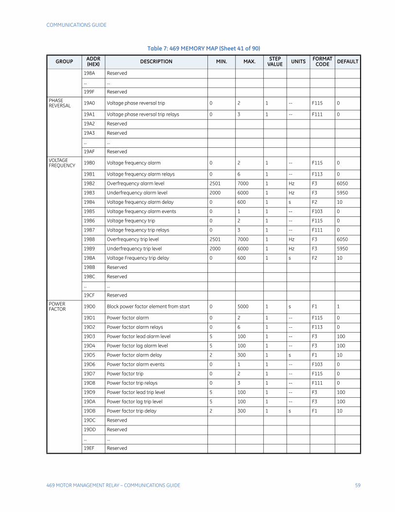
COMMUNICATIONS GUIDE
469 MOTOR MANAGEMENT RELAY – COMMUNICATIONS GUIDE 59
198A Reserved
... ...
199F Reserved
PHASE REVERSAL 19A0 Voltage phase reversal trip 0 2 1 -- F115 0
19A1 Voltage phase reversal trip relays 0 3 1 -- F111 0
19A2 Reserved
19A3 Reserved
... ...
19AF Reserved
VOLTAGE FREQUENCY 19B0 Voltage frequency alarm 0 2 1 -- F115 0
19B1 Voltage frequency alarm relays 0 6 1 -- F113 0
19B2 Overfrequency alarm level 2501 7000 1 Hz F3 6050
19B3 Underfrequency alarm level 2000 6000 1 Hz F3 5950
19B4 Voltage frequency alarm delay 0 600 1 s F2 10
19B5 Voltage frequency alarm events 0 1 1 -- F103 0
19B6 Voltage frequency trip 0 2 1 -- F115 0
19B7 Voltage frequency trip relays 0 3 1 -- F111 0
19B8 Overfrequency trip level 2501 7000 1 Hz F3 6050
19B9 Underfrequency trip level 2000 6000 1 Hz F3 5950
19BA Voltage Frequency trip delay 0 600 1 s F2 10
19BB Reserved
19BC Reserved
... ...
19CF Reserved
POWERFACTOR 19D0 Block power factor element from start 0 5000 1 s F1 1
19D1 Power factor alarm 0 2 1 -- F115 0
19D2 Power factor alarm relays 0 6 1 -- F113 0
19D3 Power factor lead alarm level 5 100 1 -- F3 100
19D4 Power factor lag alarm level 5 100 1 -- F3 100
19D5 Power factor alarm delay 2 300 1 s F1 10
19D6 Power factor alarm events 0 1 1 -- F103 0
19D7 Power factor trip 0 2 1 -- F115 0
19D8 Power factor trip relays 0 3 1 -- F111 0
19D9 Power factor lead trip level 5 100 1 -- F3 100
19DA Power factor lag trip level 5 100 1 -- F3 100
19DB Power factor trip delay 2 300 1 s F1 10
19DC Reserved
19DD Reserved
... ...
19EF Reserved
Table 7: 469 MEMORY MAP (Sheet 41 of 90)
GROUP ADDR(HEX) DESCRIPTION MIN. MAX. STEP
VALUE UNITS FORMATCODE DEFAULT
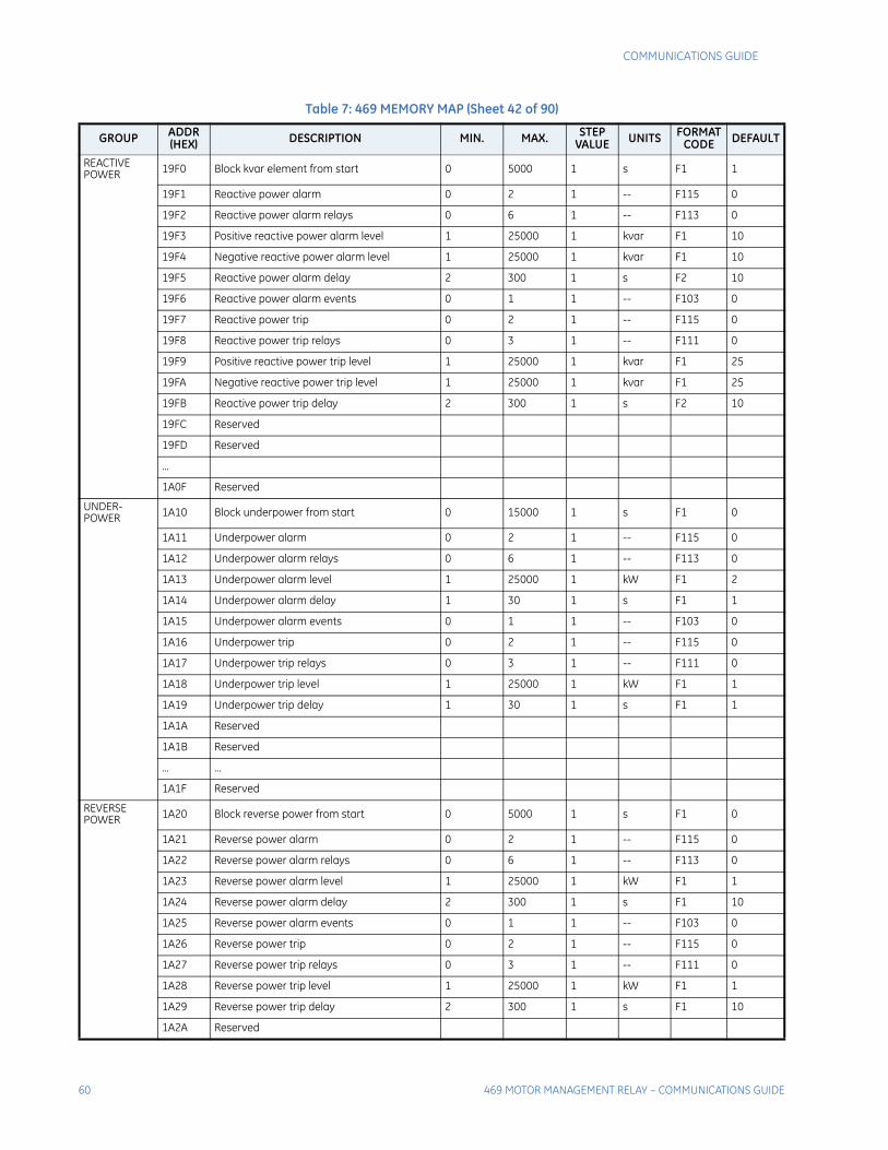
60 469 MOTOR MANAGEMENT RELAY – COMMUNICATIONS GUIDE
COMMUNICATIONS GUIDE
REACTIVE POWER 19F0 Block kvar element from start 0 5000 1 s F1 1
19F1 Reactive power alarm 0 2 1 -- F115 0
19F2 Reactive power alarm relays 0 6 1 -- F113 0
19F3 Positive reactive power alarm level 1 25000 1 kvar F1 10
19F4 Negative reactive power alarm level 1 25000 1 kvar F1 10
19F5 Reactive power alarm delay 2 300 1 s F2 10
19F6 Reactive power alarm events 0 1 1 -- F103 0
19F7 Reactive power trip 0 2 1 -- F115 0
19F8 Reactive power trip relays 0 3 1 -- F111 0
19F9 Positive reactive power trip level 1 25000 1 kvar F1 25
19FA Negative reactive power trip level 1 25000 1 kvar F1 25
19FB Reactive power trip delay 2 300 1 s F2 10
19FC Reserved
19FD Reserved
...
1A0F Reserved
UNDER-POWER 1A10 Block underpower from start 0 15000 1 s F1 0
1A11 Underpower alarm 0 2 1 -- F115 0
1A12 Underpower alarm relays 0 6 1 -- F113 0
1A13 Underpower alarm level 1 25000 1 kW F1 2
1A14 Underpower alarm delay 1 30 1 s F1 1
1A15 Underpower alarm events 0 1 1 -- F103 0
1A16 Underpower trip 0 2 1 -- F115 0
1A17 Underpower trip relays 0 3 1 -- F111 0
1A18 Underpower trip level 1 25000 1 kW F1 1
1A19 Underpower trip delay 1 30 1 s F1 1
1A1A Reserved
1A1B Reserved
... ...
1A1F Reserved
REVERSE POWER 1A20 Block reverse power from start 0 5000 1 s F1 0
1A21 Reverse power alarm 0 2 1 -- F115 0
1A22 Reverse power alarm relays 0 6 1 -- F113 0
1A23 Reverse power alarm level 1 25000 1 kW F1 1
1A24 Reverse power alarm delay 2 300 1 s F1 10
1A25 Reverse power alarm events 0 1 1 -- F103 0
1A26 Reverse power trip 0 2 1 -- F115 0
1A27 Reverse power trip relays 0 3 1 -- F111 0
1A28 Reverse power trip level 1 25000 1 kW F1 1
1A29 Reverse power trip delay 2 300 1 s F1 10
1A2A Reserved
Table 7: 469 MEMORY MAP (Sheet 42 of 90)
GROUP ADDR(HEX) DESCRIPTION MIN. MAX. STEP
VALUE UNITS FORMATCODE DEFAULT
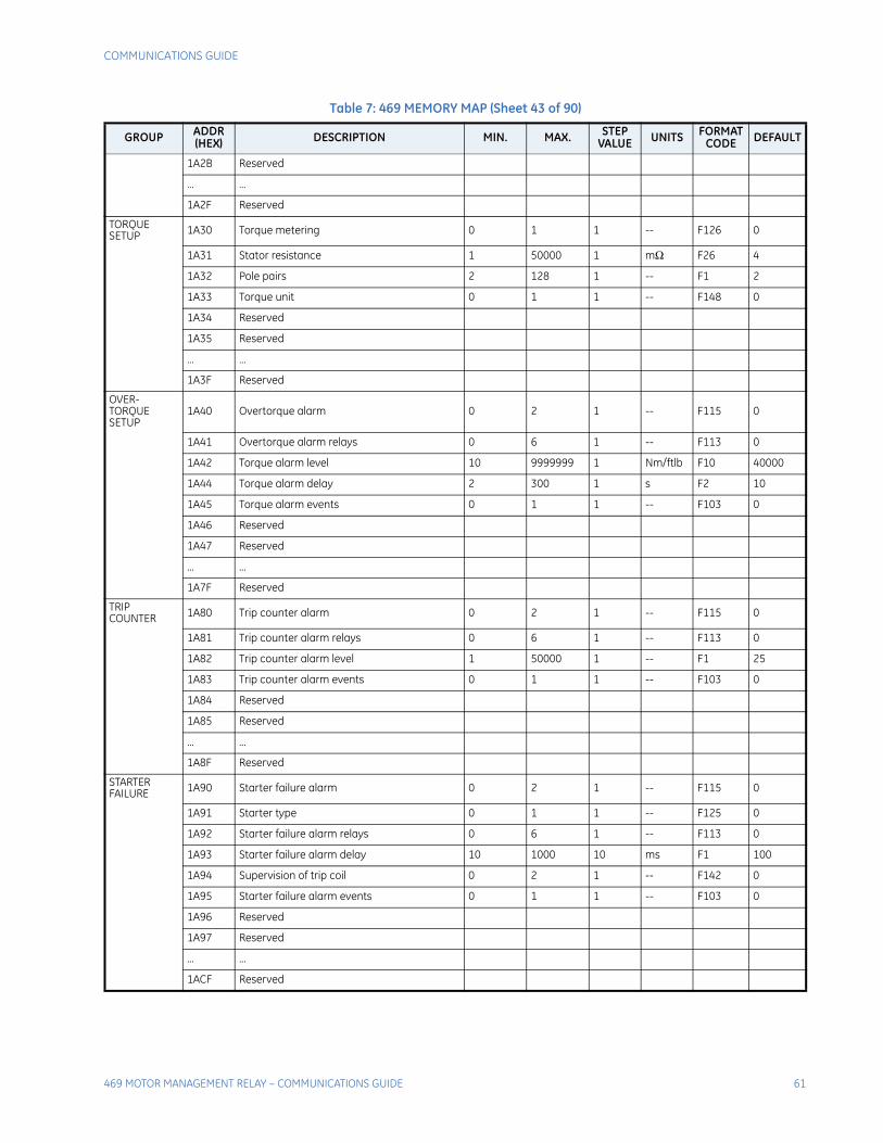
COMMUNICATIONS GUIDE
469 MOTOR MANAGEMENT RELAY – COMMUNICATIONS GUIDE 61
1A2B Reserved
… …
1A2F Reserved
TORQUE SETUP 1A30 Torque metering 0 1 1 -- F126 0
1A31 Stator resistance 1 50000 1 mΩ F26 4
1A32 Pole pairs 2 128 1 -- F1 2
1A33 Torque unit 0 1 1 -- F148 0
1A34 Reserved
1A35 Reserved
… …
1A3F Reserved
OVER-TORQUESETUP
1A40 Overtorque alarm 0 2 1 -- F115 0
1A41 Overtorque alarm relays 0 6 1 -- F113 0
1A42 Torque alarm level 10 9999999 1 Nm/ftlb F10 40000
1A44 Torque alarm delay 2 300 1 s F2 10
1A45 Torque alarm events 0 1 1 -- F103 0
1A46 Reserved
1A47 Reserved
... ...
1A7F Reserved
TRIP COUNTER 1A80 Trip counter alarm 0 2 1 -- F115 0
1A81 Trip counter alarm relays 0 6 1 -- F113 0
1A82 Trip counter alarm level 1 50000 1 -- F1 25
1A83 Trip counter alarm events 0 1 1 -- F103 0
1A84 Reserved
1A85 Reserved
... ...
1A8F Reserved
STARTER FAILURE 1A90 Starter failure alarm 0 2 1 -- F115 0
1A91 Starter type 0 1 1 -- F125 0
1A92 Starter failure alarm relays 0 6 1 -- F113 0
1A93 Starter failure alarm delay 10 1000 10 ms F1 100
1A94 Supervision of trip coil 0 2 1 -- F142 0
1A95 Starter failure alarm events 0 1 1 -- F103 0
1A96 Reserved
1A97 Reserved
... ...
1ACF Reserved
Table 7: 469 MEMORY MAP (Sheet 43 of 90)
GROUP ADDR(HEX) DESCRIPTION MIN. MAX. STEP
VALUE UNITS FORMATCODE DEFAULT
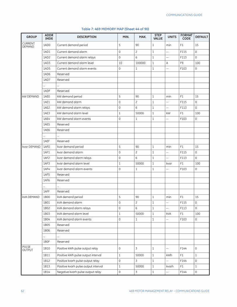
62 469 MOTOR MANAGEMENT RELAY – COMMUNICATIONS GUIDE
COMMUNICATIONS GUIDE
CURRENT DEMAND 1AD0 Current demand period 5 90 1 min F1 15
1AD1 Current demand alarm 0 2 1 -- F115 0
1AD2 Current demand alarm relays 0 6 1 -- F113 0
1AD3 Current demand alarm level 10 100000 1 A F9 100
1AD5 Current demand alarm events 0 1 1 -- F103 0
1AD6 Reserved
1AD7 Reserved
... ...
1ADF Reserved
kW DEMAND 1AE0 kW demand period 5 90 1 min F1 15
1AE1 kW demand alarm 0 2 1 -- F115 0
1AE2 kW demand alarm relays 0 6 1 -- F113 0
1AE3 kW demand alarm level 1 50000 1 kW F1 100
1AE4 kW demand alarm events 0 1 1 -- F103 0
1AE5 Reserved
1AE6 Reserved
... ...
1AEF Reserved
kvar DEMAND 1AF0 kvar demand period 5 90 1 min F1 15
1AF1 kvar demand alarm 0 2 1 -- F115 0
1AF2 kvar demand alarm relays 0 6 1 -- F113 0
1AF3 kvar demand alarm level 1 50000 1 kvar F1 100
1AF4 kvar demand alarm events 0 1 1 -- F103 0
1AF5 Reserved
1AF6 Reserved
... ...
1AFF Reserved
kVA DEMAND 1B00 kVA demand period 5 90 1 min F1 15
1B01 kVA demand alarm 0 2 1 -- F115 0
1B02 kVA demand alarm relays 0 6 1 -- F113 0
1B03 kVA demand alarm level 1 50000 1 kVA F1 100
1B04 kVA demand alarm events 0 1 1 -- F103 0
1B05 Reserved
1B06 Reserved
... ...
1B0F Reserved
PULSE OUTPUT 1B10 Positive kWh pulse output relay 0 3 1 -- F144 0
1B11 Positive kWh pulse output interval 1 50000 1 kWh F1 1
1B12 Positive kvarh pulse output relay 0 3 1 -- F144 0
1B13 Positive kvarh pulse output interval 1 50000 1 kvarh F1 1
1B14 Negative kvarh pulse output relay 0 3 1 -- F144 0
Table 7: 469 MEMORY MAP (Sheet 44 of 90)
GROUP ADDR(HEX) DESCRIPTION MIN. MAX. STEP
VALUE UNITS FORMATCODE DEFAULT
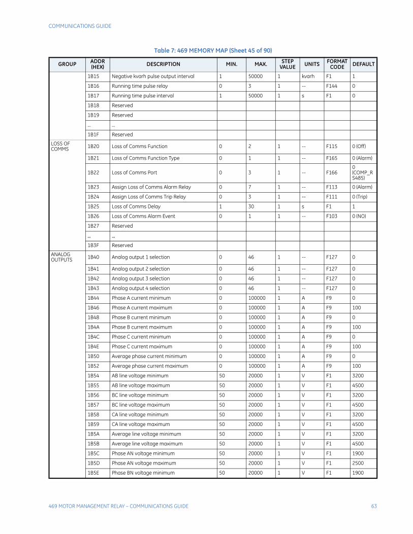
COMMUNICATIONS GUIDE
469 MOTOR MANAGEMENT RELAY – COMMUNICATIONS GUIDE 63
1B15 Negative kvarh pulse output interval 1 50000 1 kvarh F1 1
1B16 Running time pulse relay 0 3 1 -- F144 0
1B17 Running time pulse interval 1 50000 1 s F1 0
1B18 Reserved
1B19 Reserved
... ...
1B1F Reserved
LOSS OF COMMS 1B20 Loss of Comms Function 0 2 1 -- F115 0 (Off)
1B21 Loss of Comms Function Type 0 1 1 -- F165 0 (Alarm)
1B22 Loss of Comms Port 0 3 1 -- F1660 (COMP_RS485)
1B23 Assign Loss of Comms Alarm Relay 0 7 1 -- F113 0 (Alarm)
1B24 Assign Loss of Comms Trip Relay 0 3 1 -- F111 0 (Trip)
1B25 Loss of Comms Delay 1 30 1 s F1 1
1B26 Loss of Comms Alarm Event 0 1 1 -- F103 0 (NO)
1B27 Reserved
,,, ,,,
1B3F Reserved
ANALOGOUTPUTS 1B40 Analog output 1 selection 0 46 1 -- F127 0
1B41 Analog output 2 selection 0 46 1 -- F127 0
1B42 Analog output 3 selection 0 46 1 -- F127 0
1B43 Analog output 4 selection 0 46 1 -- F127 0
1B44 Phase A current minimum 0 100000 1 A F9 0
1B46 Phase A current maximum 0 100000 1 A F9 100
1B48 Phase B current minimum 0 100000 1 A F9 0
1B4A Phase B current maximum 0 100000 1 A F9 100
1B4C Phase C current minimum 0 100000 1 A F9 0
1B4E Phase C current maximum 0 100000 1 A F9 100
1B50 Average phase current minimum 0 100000 1 A F9 0
1B52 Average phase current maximum 0 100000 1 A F9 100
1B54 AB line voltage minimum 50 20000 1 V F1 3200
1B55 AB line voltage maximum 50 20000 1 V F1 4500
1B56 BC line voltage minimum 50 20000 1 V F1 3200
1B57 BC line voltage maximum 50 20000 1 V F1 4500
1B58 CA line voltage minimum 50 20000 1 V F1 3200
1B59 CA line voltage maximum 50 20000 1 V F1 4500
1B5A Average line voltage minimum 50 20000 1 V F1 3200
1B5B Average line voltage maximum 50 20000 1 V F1 4500
1B5C Phase AN voltage minimum 50 20000 1 V F1 1900
1B5D Phase AN voltage maximum 50 20000 1 V F1 2500
1B5E Phase BN voltage minimum 50 20000 1 V F1 1900
Table 7: 469 MEMORY MAP (Sheet 45 of 90)
GROUP ADDR(HEX) DESCRIPTION MIN. MAX. STEP
VALUE UNITS FORMATCODE DEFAULT
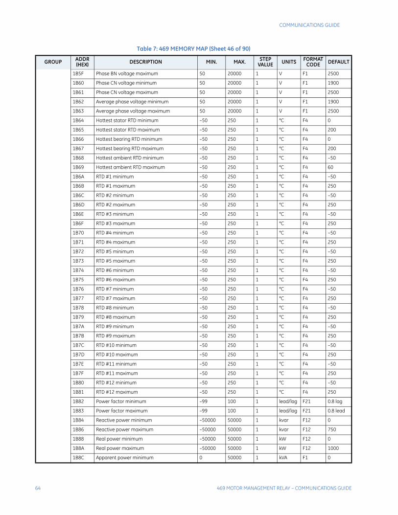
64 469 MOTOR MANAGEMENT RELAY – COMMUNICATIONS GUIDE
COMMUNICATIONS GUIDE
1B5F Phase BN voltage maximum 50 20000 1 V F1 2500
1B60 Phase CN voltage minimum 50 20000 1 V F1 1900
1B61 Phase CN voltage maximum 50 20000 1 V F1 2500
1B62 Average phase voltage minimum 50 20000 1 V F1 1900
1B63 Average phase voltage maximum 50 20000 1 V F1 2500
1B64 Hottest stator RTD minimum –50 250 1 °C F4 0
1B65 Hottest stator RTD maximum –50 250 1 °C F4 200
1B66 Hottest bearing RTD minimum –50 250 1 °C F4 0
1B67 Hottest bearing RTD maximum –50 250 1 °C F4 200
1B68 Hottest ambient RTD minimum –50 250 1 °C F4 –50
1B69 Hottest ambient RTD maximum –50 250 1 °C F4 60
1B6A RTD #1 minimum –50 250 1 °C F4 –50
1B6B RTD #1 maximum –50 250 1 °C F4 250
1B6C RTD #2 minimum –50 250 1 °C F4 –50
1B6D RTD #2 maximum –50 250 1 °C F4 250
1B6E RTD #3 minimum –50 250 1 °C F4 –50
1B6F RTD #3 maximum –50 250 1 °C F4 250
1B70 RTD #4 minimum –50 250 1 °C F4 –50
1B71 RTD #4 maximum –50 250 1 °C F4 250
1B72 RTD #5 minimum –50 250 1 °C F4 –50
1B73 RTD #5 maximum –50 250 1 °C F4 250
1B74 RTD #6 minimum –50 250 1 °C F4 –50
1B75 RTD #6 maximum –50 250 1 °C F4 250
1B76 RTD #7 minimum –50 250 1 °C F4 –50
1B77 RTD #7 maximum –50 250 1 °C F4 250
1B78 RTD #8 minimum –50 250 1 °C F4 –50
1B79 RTD #8 maximum –50 250 1 °C F4 250
1B7A RTD #9 minimum –50 250 1 °C F4 –50
1B7B RTD #9 maximum –50 250 1 °C F4 250
1B7C RTD #10 minimum –50 250 1 °C F4 –50
1B7D RTD #10 maximum –50 250 1 °C F4 250
1B7E RTD #11 minimum –50 250 1 °C F4 –50
1B7F RTD #11 maximum –50 250 1 °C F4 250
1B80 RTD #12 minimum –50 250 1 °C F4 –50
1B81 RTD #12 maximum –50 250 1 °C F4 250
1B82 Power factor minimum –99 100 1 lead/lag F21 0.8 lag
1B83 Power factor maximum –99 100 1 lead/lag F21 0.8 lead
1B84 Reactive power minimum –50000 50000 1 kvar F12 0
1B86 Reactive power maximum –50000 50000 1 kvar F12 750
1B88 Real power minimum –50000 50000 1 kW F12 0
1B8A Real power maximum –50000 50000 1 kW F12 1000
1B8C Apparent power minimum 0 50000 1 kVA F1 0
Table 7: 469 MEMORY MAP (Sheet 46 of 90)
GROUP ADDR(HEX) DESCRIPTION MIN. MAX. STEP
VALUE UNITS FORMATCODE DEFAULT
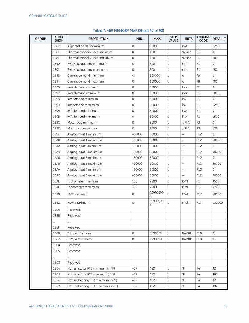
COMMUNICATIONS GUIDE
469 MOTOR MANAGEMENT RELAY – COMMUNICATIONS GUIDE 65
1B8D Apparent power maximum 0 50000 1 kVA F1 1250
1B8E Thermal capacity used minimum 0 100 1 %used F1 0
1B8F Thermal capacity used maximum 0 100 1 %used F1 100
1B90 Relay lockout time minimum 0 500 1 min F1 0
1B91 Relay lockout time maximum 0 500 1 min F1 150
1B92 Current demand minimum 0 100000 1 A F9 0
1B94 Current demand maximum 0 100000 1 A F9 700
1B96 kvar demand minimum 0 50000 1 kvar F1 0
1B97 kvar demand maximum 0 50000 1 kvar F1 1000
1B98 kW demand minimum 0 50000 1 kW F1 0
1B99 kW demand maximum 0 50000 1 kW F1 1250
1B9A kVA demand minimum 0 50000 1 kVA F1 0
1B9B kVA demand maximum 0 50000 1 kVA F1 1500
1B9C Motor load minimum 0 2000 1 × FLA F3 0
1B9D Motor load maximum 0 2000 1 × FLA F3 125
1B9E Analog input 1 minimum –50000 50000 1 -- F12 0
1BA0 Analog input 1 maximum –50000 50000 1 -- F12 50000
1BA2 Analog input 2 minimum –50000 50000 1 -- F12 0
1BA4 Analog input 2 maximum –50000 50000 1 -- F12 50000
1BA6 Analog input 3 minimum –50000 50000 1 -- F12 0
1BA8 Analog input 3 maximum –50000 50000 1 -- F12 50000
1BAA Analog input 4 minimum –50000 50000 1 -- F12 0
1BAC Analog input 4 maximum –50000 50000 1 -- F12 50000
1BAE Tachometer minimum 100 7200 1 RPM F1 3500
1BAF Tachometer maximum 100 7200 1 RPM F1 3700
1BB0 MWh minimum 0 999999999 1 MWh F17 50000
1BB2 MWh maximum 0 999999999 1 MWh F17 100000
1BB4 Reserved
1BB5 Reserved
... ...
1BBF Reserved
1BC0 Torque minimum 0 9999999 1 Nm/ftlb F10 0
1BC2 Torque maximum 0 9999999 1 Nm/ftlb F10 0
1BC4 Reserved
1BC5 Reserved
… …
1BD3 Reserved
1BD4 Hottest stator RTD minimum (in °F) –57 482 1 °F F4 32
1BD5 Hottest stator RTD maximum (in °F) –57 482 1 °F F4 392
1BD6 Hottest bearing RTD minimum (in °F) –57 482 1 °F F4 32
1BC7 Hottest bearing RTD maximum (in °F) –57 482 1 °F F4 392
Table 7: 469 MEMORY MAP (Sheet 47 of 90)
GROUP ADDR(HEX) DESCRIPTION MIN. MAX. STEP
VALUE UNITS FORMATCODE DEFAULT
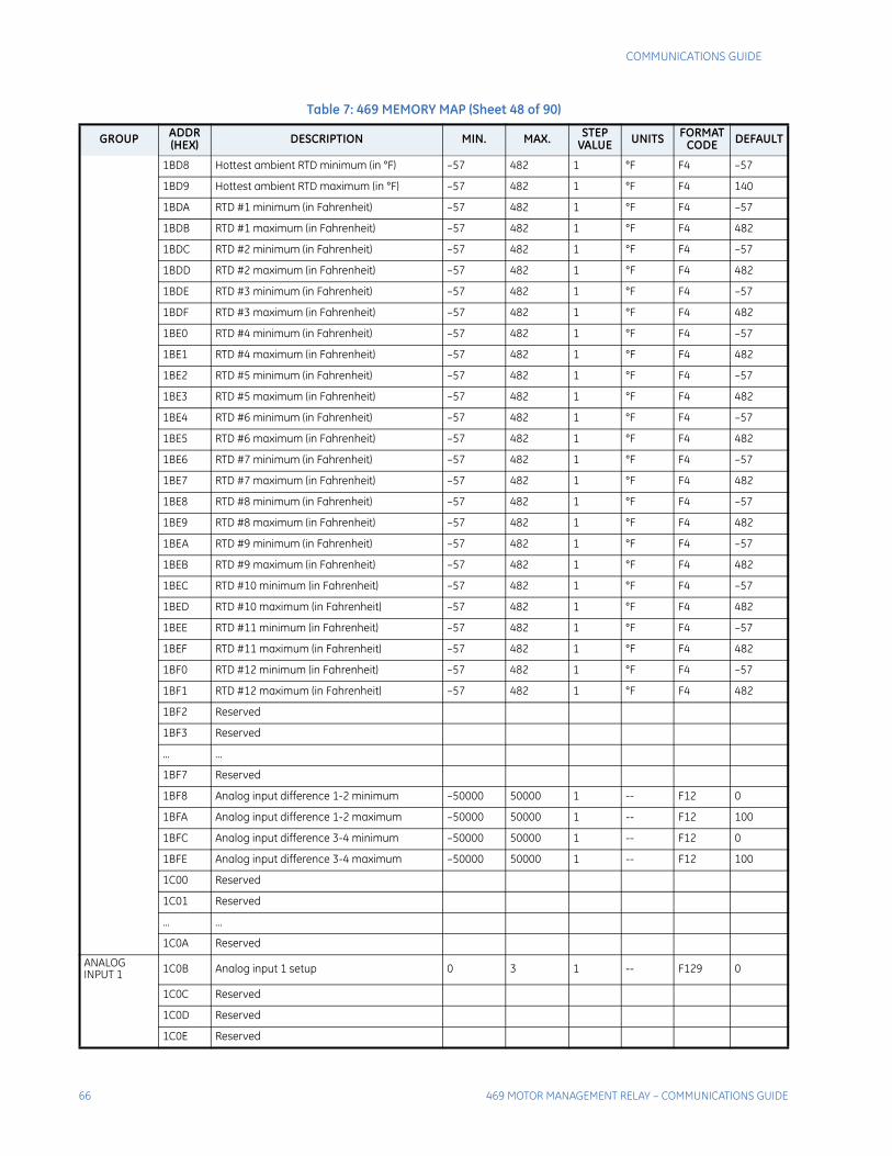
66 469 MOTOR MANAGEMENT RELAY – COMMUNICATIONS GUIDE
COMMUNICATIONS GUIDE
1BD8 Hottest ambient RTD minimum (in °F) –57 482 1 °F F4 –57
1BD9 Hottest ambient RTD maximum (in °F) –57 482 1 °F F4 140
1BDA RTD #1 minimum (in Fahrenheit) –57 482 1 °F F4 –57
1BDB RTD #1 maximum (in Fahrenheit) –57 482 1 °F F4 482
1BDC RTD #2 minimum (in Fahrenheit) –57 482 1 °F F4 –57
1BDD RTD #2 maximum (in Fahrenheit) –57 482 1 °F F4 482
1BDE RTD #3 minimum (in Fahrenheit) –57 482 1 °F F4 –57
1BDF RTD #3 maximum (in Fahrenheit) –57 482 1 °F F4 482
1BE0 RTD #4 minimum (in Fahrenheit) –57 482 1 °F F4 –57
1BE1 RTD #4 maximum (in Fahrenheit) –57 482 1 °F F4 482
1BE2 RTD #5 minimum (in Fahrenheit) –57 482 1 °F F4 –57
1BE3 RTD #5 maximum (in Fahrenheit) –57 482 1 °F F4 482
1BE4 RTD #6 minimum (in Fahrenheit) –57 482 1 °F F4 –57
1BE5 RTD #6 maximum (in Fahrenheit) –57 482 1 °F F4 482
1BE6 RTD #7 minimum (in Fahrenheit) –57 482 1 °F F4 –57
1BE7 RTD #7 maximum (in Fahrenheit) –57 482 1 °F F4 482
1BE8 RTD #8 minimum (in Fahrenheit) –57 482 1 °F F4 –57
1BE9 RTD #8 maximum (in Fahrenheit) –57 482 1 °F F4 482
1BEA RTD #9 minimum (in Fahrenheit) –57 482 1 °F F4 –57
1BEB RTD #9 maximum (in Fahrenheit) –57 482 1 °F F4 482
1BEC RTD #10 minimum (in Fahrenheit) –57 482 1 °F F4 –57
1BED RTD #10 maximum (in Fahrenheit) –57 482 1 °F F4 482
1BEE RTD #11 minimum (in Fahrenheit) –57 482 1 °F F4 –57
1BEF RTD #11 maximum (in Fahrenheit) –57 482 1 °F F4 482
1BF0 RTD #12 minimum (in Fahrenheit) –57 482 1 °F F4 –57
1BF1 RTD #12 maximum (in Fahrenheit) –57 482 1 °F F4 482
1BF2 Reserved
1BF3 Reserved
... ...
1BF7 Reserved
1BF8 Analog input difference 1-2 minimum –50000 50000 1 -- F12 0
1BFA Analog input difference 1-2 maximum –50000 50000 1 -- F12 100
1BFC Analog input difference 3-4 minimum –50000 50000 1 -- F12 0
1BFE Analog input difference 3-4 maximum –50000 50000 1 -- F12 100
1C00 Reserved
1C01 Reserved
... ...
1C0A Reserved
ANALOG INPUT 1 1C0B Analog input 1 setup 0 3 1 -- F129 0
1C0C Reserved
1C0D Reserved
1C0E Reserved
Table 7: 469 MEMORY MAP (Sheet 48 of 90)
GROUP ADDR(HEX) DESCRIPTION MIN. MAX. STEP
VALUE UNITS FORMATCODE DEFAULT
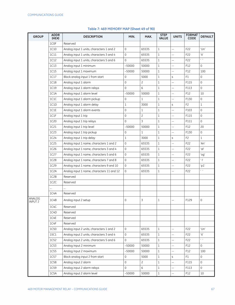
COMMUNICATIONS GUIDE
469 MOTOR MANAGEMENT RELAY – COMMUNICATIONS GUIDE 67
1C0F Reserved
1C10 Analog input 1 units, characters 1 and 2 0 65535 1 -- F22 ‘Un’
1C11 Analog input 1 units, characters 3 and 4 0 65535 1 -- F22 ‘it’
1C12 Analog input 1 units, characters 5 and 6 0 65535 1 -- F22 ‘ ’
1C13 Analog input 1 minimum –50000 50000 1 -- F12 0
1C15 Analog input 1 maximum –50000 50000 1 -- F12 100
1C17 Block analog input 1 from start 0 5000 1 s F1 0
1C18 Analog input 1 alarm 0 2 1 -- F115 0
1C19 Analog input 1 alarm relays 0 6 1 -- F113 0
1C1A Analog input 1 alarm level –50000 50000 1 -- F12 10
1C1C Analog input 1 alarm pickup 0 1 1 -- F130 0
1C1D Analog input 1 alarm delay 1 3000 1 s F2 1
1C1E Analog input 1 alarm events 0 1 1 -- F103 0
1C1F Analog input 1 trip 0 2 1 -- F115 0
1C20 Analog input 1 trip relays 0 3 1 -- F111 0
1C21 Analog input 1 trip level –50000 50000 1 -- F12 20
1C23 Analog input 1 trip pickup 0 1 1 -- F130 0
1C24 Analog input 1 trip delay 1 3000 1 s F2 1
1C25 Analog input 1 name, characters 1 and 2 0 65535 1 -- F22 ‘An’
1C26 Analog input 1 name, characters 3 and 4 0 65535 1 -- F22 ‘al’
1C27 Analog input 1 name, characters 5 and 6 0 65535 1 -- F22 ‘og’
1C28 Analog input 1 name, characters 7 and 8 0 65535 1 -- F22 ‘ I’
1C29 Analog input 1 name, characters 9 and 10 0 65535 1 -- F22 ‘p1’
1C2A Analog input 1 name, characters 11 and 12 0 65535 1 -- F22 ‘ ’
1C2B Reserved
1C2C Reserved
... ...
1C4A Reserved
ANALOG INPUT 2 1C4B Analog input 2 setup 0 3 1 -- F129 0
1C4C Reserved
1C4D Reserved
1C4E Reserved
1C4F Reserved
1C50 Analog input 2 units, characters 1 and 2 0 65535 1 -- F22 ‘Un’
15C1 Analog input 2 units, characters 3 and 4 0 65535 1 -- F22 ‘it’
1C52 Analog input 2 units, characters 5 and 6 0 65535 1 -- F22 ‘ ’
1C53 Analog Input 2 minimum –50000 50000 1 -- F12 0
1C55 Analog Input 2 maximum –50000 50000 1 -- F12 100
1C57 Block analog input 2 from start 0 5000 1 s F1 0
1C58 Analog input 2 alarm 0 2 1 -- F115 0
1C59 Analog input 2 alarm relays 0 6 1 -- F113 0
1C5A Analog input 2 alarm level –50000 50000 1 -- F12 10
Table 7: 469 MEMORY MAP (Sheet 49 of 90)
GROUP ADDR(HEX) DESCRIPTION MIN. MAX. STEP
VALUE UNITS FORMATCODE DEFAULT
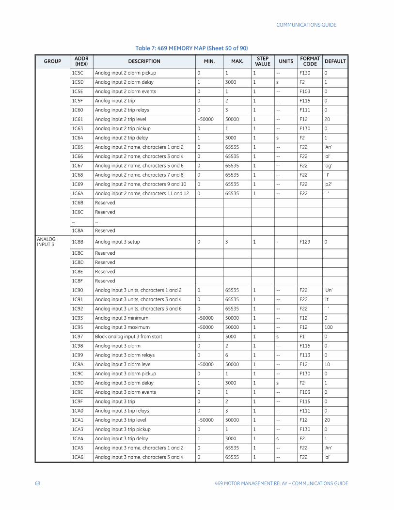
68 469 MOTOR MANAGEMENT RELAY – COMMUNICATIONS GUIDE
COMMUNICATIONS GUIDE
1C5C Analog input 2 alarm pickup 0 1 1 -- F130 0
1C5D Analog input 2 alarm delay 1 3000 1 s F2 1
1C5E Analog input 2 alarm events 0 1 1 -- F103 0
1C5F Analog input 2 trip 0 2 1 -- F115 0
1C60 Analog input 2 trip relays 0 3 1 -- F111 0
1C61 Analog input 2 trip level –50000 50000 1 -- F12 20
1C63 Analog input 2 trip pickup 0 1 1 -- F130 0
1C64 Analog input 2 trip delay 1 3000 1 s F2 1
1C65 Analog input 2 name, characters 1 and 2 0 65535 1 -- F22 ‘An’
1C66 Analog input 2 name, characters 3 and 4 0 65535 1 -- F22 ‘al’
1C67 Analog input 2 name, characters 5 and 6 0 65535 1 -- F22 ‘og’
1C68 Analog input 2 name, characters 7 and 8 0 65535 1 -- F22 ‘ I’
1C69 Analog input 2 name, characters 9 and 10 0 65535 1 -- F22 ‘p2’
1C6A Analog input 2 name, characters 11 and 12 0 65535 1 -- F22 ‘ ’
1C6B Reserved
1C6C Reserved
... ...
1C8A Reserved
ANALOG INPUT 3 1C8B Analog input 3 setup 0 3 1 - F129 0
1C8C Reserved
1C8D Reserved
1C8E Reserved
1C8F Reserved
1C90 Analog input 3 units, characters 1 and 2 0 65535 1 -- F22 ‘Un’
1C91 Analog input 3 units, characters 3 and 4 0 65535 1 -- F22 ‘it’
1C92 Analog input 3 units, characters 5 and 6 0 65535 1 -- F22 ‘ ’
1C93 Analog input 3 minimum –50000 50000 1 -- F12 0
1C95 Analog input 3 maximum –50000 50000 1 -- F12 100
1C97 Block analog input 3 from start 0 5000 1 s F1 0
1C98 Analog input 3 alarm 0 2 1 -- F115 0
1C99 Analog input 3 alarm relays 0 6 1 -- F113 0
1C9A Analog input 3 alarm level –50000 50000 1 -- F12 10
1C9C Analog input 3 alarm pickup 0 1 1 -- F130 0
1C9D Analog input 3 alarm delay 1 3000 1 s F2 1
1C9E Analog input 3 alarm events 0 1 1 -- F103 0
1C9F Analog input 3 trip 0 2 1 -- F115 0
1CA0 Analog input 3 trip relays 0 3 1 -- F111 0
1CA1 Analog input 3 trip level –50000 50000 1 -- F12 20
1CA3 Analog input 3 trip pickup 0 1 1 -- F130 0
1CA4 Analog input 3 trip delay 1 3000 1 s F2 1
1CA5 Analog input 3 name, characters 1 and 2 0 65535 1 -- F22 ‘An’
1CA6 Analog input 3 name, characters 3 and 4 0 65535 1 -- F22 ‘al’
Table 7: 469 MEMORY MAP (Sheet 50 of 90)
GROUP ADDR(HEX) DESCRIPTION MIN. MAX. STEP
VALUE UNITS FORMATCODE DEFAULT
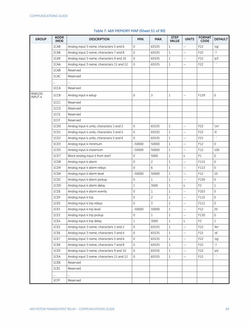
COMMUNICATIONS GUIDE
469 MOTOR MANAGEMENT RELAY – COMMUNICATIONS GUIDE 69
1CA8 Analog input 3 name, characters 5 and 6 0 65535 1 -- F22 ‘og’
1CA8 Analog input 3 name, characters 7 and 8 0 65535 1 -- F22 ‘ I’
1CA9 Analog input 3 name, characters 9 and 10 0 65535 1 -- F22 ‘p3’
1CAA Analog input 3 name, characters 11 and 12 0 65535 1 -- F22 ‘ ’
1CAB Reserved
1CAC Reserved
... ...
1CCA Reserved
ANALOG INPUT 4 1CCB Analog input 4 setup 0 3 1 -- F129 0
1CCC Reserved
1CCD Reserved
1CCE Reserved
1CCF Reserved
1CD0 Analog input 4 units, characters 1 and 2 0 65535 1 -- F22 ‘Un’
1CD1 Analog input 4 units, characters 3 and 4 0 65535 1 -- F22 ‘it’
1CD2 Analog input 4 units, characters 5 and 6 0 65535 1 -- F22 ‘ ’
1CD3 Analog input 4 minimum –50000 50000 1 -- F12 0
1CD5 Analog input 4 maximum –50000 50000 1 -- F12 100
1CD7 Block analog input 4 from start 0 5000 1 s F1 0
1CD8 Analog input 4 alarm 0 2 1 -- F115 0
1CD9 Analog input 4 alarm relays 0 6 1 -- F113 0
1CDA Analog input 4 alarm level –50000 50000 1 -- F12 10
1CDC Analog input 4 alarm pickup 0 1 1 -- F130 0
1CDD Analog input 4 alarm delay 1 3000 1 s F2 1
1CDE Analog input 4 alarm events 0 1 1 -- F103 0
1CDF Analog input 4 trip 0 2 1 -- F115 0
1CE0 Analog input 4 trip relays 0 3 1 -- F111 0
1CE1 Analog input 4 trip level –50000 50000 1 -- F12 20
1CE3 Analog input 4 trip pickup 0 1 1 -- F130 0
1CE4 Analog input 4 trip delay 1 3000 1 s F2 1
1CE5 Analog input 3 name, characters 1 and 2 0 65535 1 -- F22 ‘An’
1CE6 Analog input 3 name, characters 3 and 4 0 65535 1 -- F22 ‘al’
1CE7 Analog input 3 name, characters 5 and 6 0 65535 1 -- F22 ‘og’
1CE8 Analog input 3 name, characters 7 and 8 0 65535 1 -- F22 ‘ I’
1CE9 Analog input 3 name, characters 9 and 10 0 65535 1 -- F22 ‘p4’
1CEA Analog input 3 name, characters 11 and 12 0 65535 1 -- F22 ‘ ’
1CEB Reserved
1CEC Reserved
... ...
1CFF Reserved
Table 7: 469 MEMORY MAP (Sheet 51 of 90)
GROUP ADDR(HEX) DESCRIPTION MIN. MAX. STEP
VALUE UNITS FORMATCODE DEFAULT
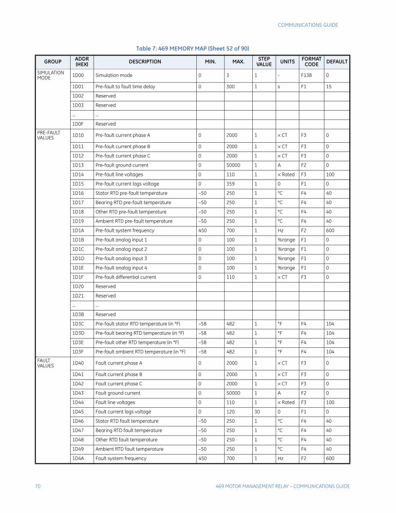
70 469 MOTOR MANAGEMENT RELAY – COMMUNICATIONS GUIDE
COMMUNICATIONS GUIDE
SIMULATION MODE 1D00 Simulation mode 0 3 1 - F138 0
1D01 Pre-fault to fault time delay 0 300 1 s F1 15
1D02 Reserved
1D03 Reserved
... ...
1D0F Reserved
PRE-FAULT VALUES 1D10 Pre-fault current phase A 0 2000 1 × CT F3 0
1D11 Pre-fault current phase B 0 2000 1 × CT F3 0
1D12 Pre-fault current phase C 0 2000 1 × CT F3 0
1D13 Pre-fault ground current 0 50000 1 A F2 0
1D14 Pre-fault line voltages 0 110 1 × Rated F3 100
1D15 Pre-fault current lags voltage 0 359 1 0 F1 0
1D16 Stator RTD pre-fault temperature –50 250 1 °C F4 40
1D17 Bearing RTD pre-fault temperature –50 250 1 °C F4 40
1D18 Other RTD pre-fault temperature –50 250 1 °C F4 40
1D19 Ambient RTD pre-fault temperature –50 250 1 °C F4 40
1D1A Pre-fault system frequency 450 700 1 Hz F2 600
1D1B Pre-fault analog input 1 0 100 1 %range F1 0
1D1C Pre-fault analog input 2 0 100 1 %range F1 0
1D1D Pre-fault analog input 3 0 100 1 %range F1 0
1D1E Pre-fault analog input 4 0 100 1 %range F1 0
1D1F Pre-fault differential current 0 110 1 × CT F3 0
1D20 Reserved
1D21 Reserved
... ...
1D3B Reserved
1D3C Pre-fault stator RTD temperature (in °F) –58 482 1 °F F4 104
1D3D Pre-fault bearing RTD temperature (in °F) –58 482 1 °F F4 104
1D3E Pre-fault other RTD temperature (in °F) –58 482 1 °F F4 104
1D3F Pre-fault ambient RTD temperature (in °F) –58 482 1 °F F4 104
FAULTVALUES 1D40 Fault current phase A 0 2000 1 × CT F3 0
1D41 Fault current phase B 0 2000 1 × CT F3 0
1D42 Fault current phase C 0 2000 1 × CT F3 0
1D43 Fault ground current 0 50000 1 A F2 0
1D44 Fault line voltages 0 110 1 × Rated F3 100
1D45 Fault current lags voltage 0 120 30 0 F1 0
1D46 Stator RTD fault temperature –50 250 1 °C F4 40
1D47 Bearing RTD fault temperature –50 250 1 °C F4 40
1D48 Other RTD fault temperature –50 250 1 °C F4 40
1D49 Ambient RTD fault temperature –50 250 1 °C F4 40
1D4A Fault system frequency 450 700 1 Hz F2 600
Table 7: 469 MEMORY MAP (Sheet 52 of 90)
GROUP ADDR(HEX) DESCRIPTION MIN. MAX. STEP
VALUE UNITS FORMATCODE DEFAULT
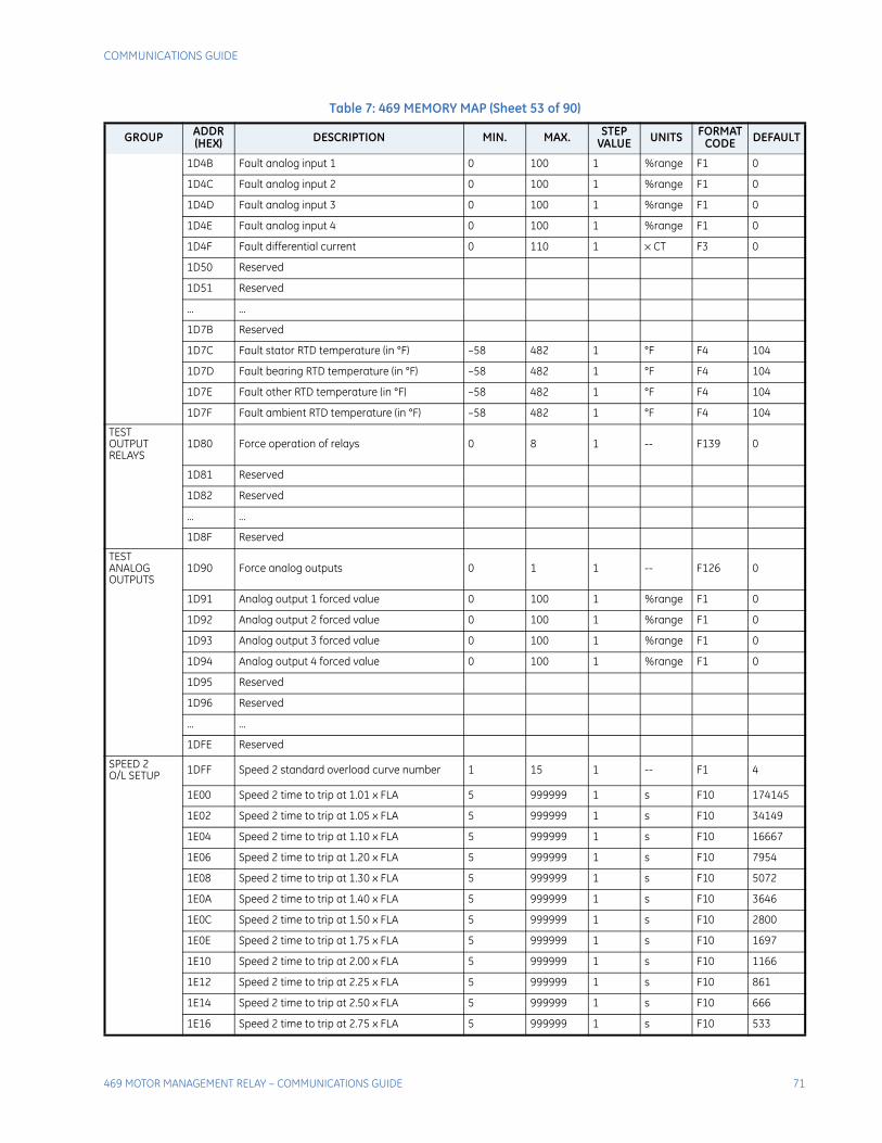
COMMUNICATIONS GUIDE
469 MOTOR MANAGEMENT RELAY – COMMUNICATIONS GUIDE 71
1D4B Fault analog input 1 0 100 1 %range F1 0
1D4C Fault analog input 2 0 100 1 %range F1 0
1D4D Fault analog input 3 0 100 1 %range F1 0
1D4E Fault analog input 4 0 100 1 %range F1 0
1D4F Fault differential current 0 110 1 × CT F3 0
1D50 Reserved
1D51 Reserved
... ...
1D7B Reserved
1D7C Fault stator RTD temperature (in °F) –58 482 1 °F F4 104
1D7D Fault bearing RTD temperature (in °F) –58 482 1 °F F4 104
1D7E Fault other RTD temperature (in °F) –58 482 1 °F F4 104
1D7F Fault ambient RTD temperature (in °F) –58 482 1 °F F4 104
TESTOUTPUT RELAYS
1D80 Force operation of relays 0 8 1 -- F139 0
1D81 Reserved
1D82 Reserved
... ...
1D8F Reserved
TESTANALOG OUTPUTS
1D90 Force analog outputs 0 1 1 -- F126 0
1D91 Analog output 1 forced value 0 100 1 %range F1 0
1D92 Analog output 2 forced value 0 100 1 %range F1 0
1D93 Analog output 3 forced value 0 100 1 %range F1 0
1D94 Analog output 4 forced value 0 100 1 %range F1 0
1D95 Reserved
1D96 Reserved
... ...
1DFE Reserved
SPEED 2O/L SETUP 1DFF Speed 2 standard overload curve number 1 15 1 -- F1 4
1E00 Speed 2 time to trip at 1.01 x FLA 5 999999 1 s F10 174145
1E02 Speed 2 time to trip at 1.05 x FLA 5 999999 1 s F10 34149
1E04 Speed 2 time to trip at 1.10 x FLA 5 999999 1 s F10 16667
1E06 Speed 2 time to trip at 1.20 x FLA 5 999999 1 s F10 7954
1E08 Speed 2 time to trip at 1.30 x FLA 5 999999 1 s F10 5072
1E0A Speed 2 time to trip at 1.40 x FLA 5 999999 1 s F10 3646
1E0C Speed 2 time to trip at 1.50 x FLA 5 999999 1 s F10 2800
1E0E Speed 2 time to trip at 1.75 x FLA 5 999999 1 s F10 1697
1E10 Speed 2 time to trip at 2.00 x FLA 5 999999 1 s F10 1166
1E12 Speed 2 time to trip at 2.25 x FLA 5 999999 1 s F10 861
1E14 Speed 2 time to trip at 2.50 x FLA 5 999999 1 s F10 666
1E16 Speed 2 time to trip at 2.75 x FLA 5 999999 1 s F10 533
Table 7: 469 MEMORY MAP (Sheet 53 of 90)
GROUP ADDR(HEX) DESCRIPTION MIN. MAX. STEP
VALUE UNITS FORMATCODE DEFAULT
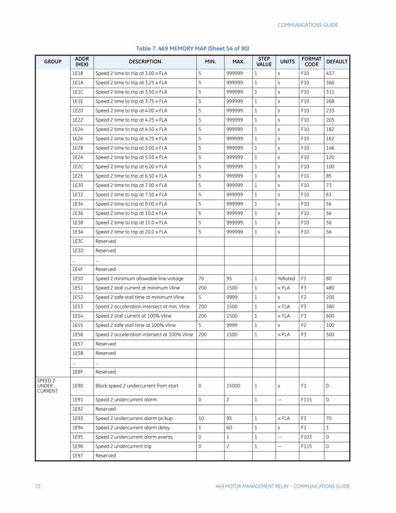
72 469 MOTOR MANAGEMENT RELAY – COMMUNICATIONS GUIDE
COMMUNICATIONS GUIDE
1E18 Speed 2 time to trip at 3.00 x FLA 5 999999 1 s F10 437
1E1A Speed 2 time to trip at 3.25 x FLA 5 999999 1 s F10 366
1E1C Speed 2 time to trip at 3.50 x FLA 5 999999 1 s F10 311
1E1E Speed 2 time to trip at 3.75 x FLA 5 999999 1 s F10 268
1E20 Speed 2 time to trip at 4.00 x FLA 5 999999 1 s F10 233
1E22 Speed 2 time to trip at 4.25 x FLA 5 999999 1 s F10 205
1E24 Speed 2 time to trip at 4.50 x FLA 5 999999 1 s F10 182
1E26 Speed 2 time to trip at 4.75 x FLA 5 999999 1 s F10 162
1E28 Speed 2 time to trip at 5.00 x FLA 5 999999 1 s F10 146
1E2A Speed 2 time to trip at 5.50 x FLA 5 999999 1 s F10 120
1E2C Speed 2 time to trip at 6.00 x FLA 5 999999 1 s F10 100
1E2E Speed 2 time to trip at 6.50 x FLA 5 999999 1 s F10 85
1E30 Speed 2 time to trip at 7.00 x FLA 5 999999 1 s F10 73
1E32 Speed 2 time to trip at 7.50 x FLA 5 999999 1 s F10 63
1E34 Speed 2 time to trip at 8.00 x FLA 5 999999 1 s F10 56
1E36 Speed 2 time to trip at 10.0 x FLA 5 999999 1 s F10 56
1E38 Speed 2 time to trip at 15.0 x FLA 5 999999 1 s F10 56
1E3A Speed 2 time to trip at 20.0 x FLA 5 999999 1 s F10 56
1E3C Reserved
1E3D Reserved
... ...
1E4F Reserved
1E50 Speed 2 minimum allowable line voltage 70 95 1 %Rated F1 80
1E51 Speed 2 stall current at minimum Vline 200 1500 1 × FLA F3 480
1E52 Speed 2 safe stall time at minimum Vline 5 9999 1 s F2 200
1E53 Speed 2 acceleration intersect at min. Vline 200 1500 1 × FLA F3 380
1E54 Speed 2 stall current at 100% Vline 200 1500 1 × FLA F3 600
1E55 Speed 2 safe stall time at 100% Vline 5 9999 1 s F2 100
1E56 Speed 2 acceleration intersect at 100% Vline 200 1500 1 × FLA F3 500
1E57 Reserved
1E58 Reserved
... ...
1E8F Reserved
SPEED 2 UNDERCURRENT
1E90 Block speed 2 undercurrent from start 0 15000 1 s F1 0
1E91 Speed 2 undercurrent alarm 0 2 1 -- F115 0
1E92 Reserved
1E93 Speed 2 undercurrent alarm pickup 10 95 1 × FLA F3 70
1E94 Speed 2 undercurrent alarm delay 1 60 1 s F1 1
1E95 Speed 2 undercurrent alarm events 0 1 1 -- F103 0
1E96 Speed 2 undercurrent trip 0 2 1 -- F115 0
1E97 Reserved
Table 7: 469 MEMORY MAP (Sheet 54 of 90)
GROUP ADDR(HEX) DESCRIPTION MIN. MAX. STEP
VALUE UNITS FORMATCODE DEFAULT
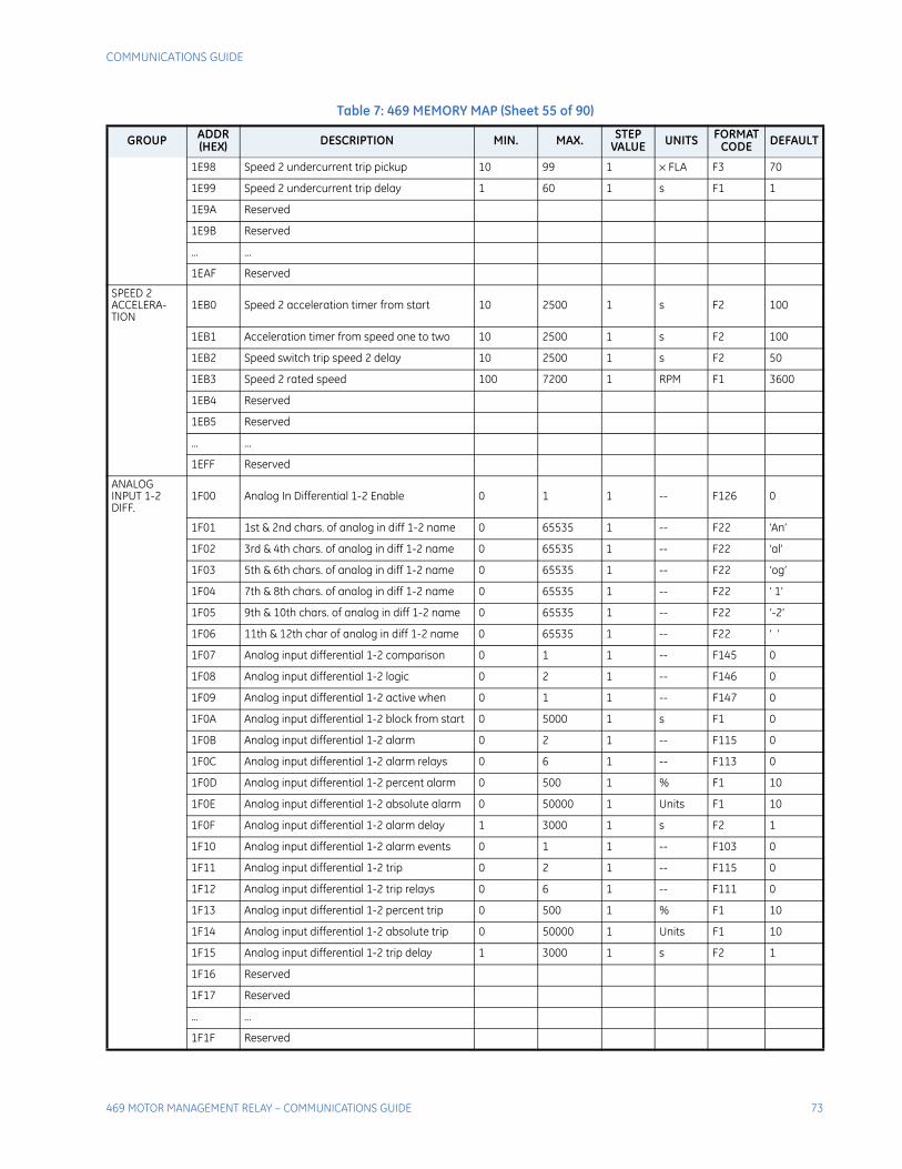
COMMUNICATIONS GUIDE
469 MOTOR MANAGEMENT RELAY – COMMUNICATIONS GUIDE 73
1E98 Speed 2 undercurrent trip pickup 10 99 1 × FLA F3 70
1E99 Speed 2 undercurrent trip delay 1 60 1 s F1 1
1E9A Reserved
1E9B Reserved
... ...
1EAF Reserved
SPEED 2 ACCELERA-TION
1EB0 Speed 2 acceleration timer from start 10 2500 1 s F2 100
1EB1 Acceleration timer from speed one to two 10 2500 1 s F2 100
1EB2 Speed switch trip speed 2 delay 10 2500 1 s F2 50
1EB3 Speed 2 rated speed 100 7200 1 RPM F1 3600
1EB4 Reserved
1EB5 Reserved
... ...
1EFF Reserved
ANALOG INPUT 1-2 DIFF.
1F00 Analog In Differential 1-2 Enable 0 1 1 -- F126 0
1F01 1st & 2nd chars. of analog in diff 1-2 name 0 65535 1 -- F22 ‘An’
1F02 3rd & 4th chars. of analog in diff 1-2 name 0 65535 1 -- F22 ‘al’
1F03 5th & 6th chars. of analog in diff 1-2 name 0 65535 1 -- F22 ‘og’
1F04 7th & 8th chars. of analog in diff 1-2 name 0 65535 1 -- F22 ‘ 1’
1F05 9th & 10th chars. of analog in diff 1-2 name 0 65535 1 -- F22 ‘-2’
1F06 11th & 12th char of analog in diff 1-2 name 0 65535 1 -- F22 ‘ ’
1F07 Analog input differential 1-2 comparison 0 1 1 -- F145 0
1F08 Analog input differential 1-2 logic 0 2 1 -- F146 0
1F09 Analog input differential 1-2 active when 0 1 1 -- F147 0
1F0A Analog input differential 1-2 block from start 0 5000 1 s F1 0
1F0B Analog input differential 1-2 alarm 0 2 1 -- F115 0
1F0C Analog input differential 1-2 alarm relays 0 6 1 -- F113 0
1F0D Analog input differential 1-2 percent alarm 0 500 1 % F1 10
1F0E Analog input differential 1-2 absolute alarm 0 50000 1 Units F1 10
1F0F Analog input differential 1-2 alarm delay 1 3000 1 s F2 1
1F10 Analog input differential 1-2 alarm events 0 1 1 -- F103 0
1F11 Analog input differential 1-2 trip 0 2 1 -- F115 0
1F12 Analog input differential 1-2 trip relays 0 6 1 -- F111 0
1F13 Analog input differential 1-2 percent trip 0 500 1 % F1 10
1F14 Analog input differential 1-2 absolute trip 0 50000 1 Units F1 10
1F15 Analog input differential 1-2 trip delay 1 3000 1 s F2 1
1F16 Reserved
1F17 Reserved
... ...
1F1F Reserved
Table 7: 469 MEMORY MAP (Sheet 55 of 90)
GROUP ADDR(HEX) DESCRIPTION MIN. MAX. STEP
VALUE UNITS FORMATCODE DEFAULT
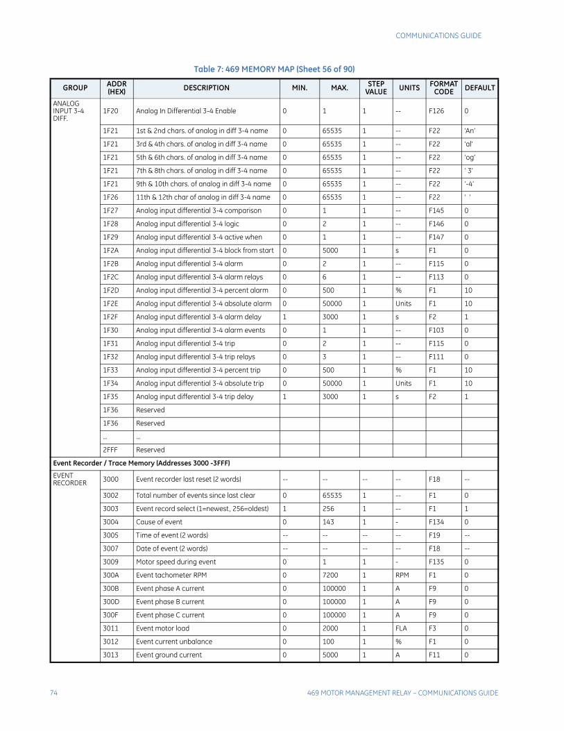
74 469 MOTOR MANAGEMENT RELAY – COMMUNICATIONS GUIDE
COMMUNICATIONS GUIDE
ANALOG INPUT 3-4DIFF.
1F20 Analog In Differential 3-4 Enable 0 1 1 -- F126 0
1F21 1st & 2nd chars. of analog in diff 3-4 name 0 65535 1 -- F22 ‘An’
1F21 3rd & 4th chars. of analog in diff 3-4 name 0 65535 1 -- F22 ‘al’
1F21 5th & 6th chars. of analog in diff 3-4 name 0 65535 1 -- F22 ‘og’
1F21 7th & 8th chars. of analog in diff 3-4 name 0 65535 1 -- F22 ‘ 3’
1F21 9th & 10th chars. of analog in diff 3-4 name 0 65535 1 -- F22 ‘-4’
1F26 11th & 12th char of analog in diff 3-4 name 0 65535 1 -- F22 ‘ ’
1F27 Analog input differential 3-4 comparison 0 1 1 -- F145 0
1F28 Analog input differential 3-4 logic 0 2 1 -- F146 0
1F29 Analog input differential 3-4 active when 0 1 1 -- F147 0
1F2A Analog input differential 3-4 block from start 0 5000 1 s F1 0
1F2B Analog input differential 3-4 alarm 0 2 1 -- F115 0
1F2C Analog input differential 3-4 alarm relays 0 6 1 -- F113 0
1F2D Analog input differential 3-4 percent alarm 0 500 1 % F1 10
1F2E Analog input differential 3-4 absolute alarm 0 50000 1 Units F1 10
1F2F Analog input differential 3-4 alarm delay 1 3000 1 s F2 1
1F30 Analog input differential 3-4 alarm events 0 1 1 -- F103 0
1F31 Analog input differential 3-4 trip 0 2 1 -- F115 0
1F32 Analog input differential 3-4 trip relays 0 3 1 -- F111 0
1F33 Analog input differential 3-4 percent trip 0 500 1 % F1 10
1F34 Analog input differential 3-4 absolute trip 0 50000 1 Units F1 10
1F35 Analog input differential 3-4 trip delay 1 3000 1 s F2 1
1F36 Reserved
1F36 Reserved
... ...
2FFF Reserved
Event Recorder / Trace Memory (Addresses 3000 -3FFF)
EVENTRECORDER 3000 Event recorder last reset (2 words) -- -- -- -- F18 --
3002 Total number of events since last clear 0 65535 1 -- F1 0
3003 Event record select (1=newest, 256=oldest) 1 256 1 -- F1 1
3004 Cause of event 0 143 1 - F134 0
3005 Time of event (2 words) -- -- -- -- F19 --
3007 Date of event (2 words) -- -- -- -- F18 --
3009 Motor speed during event 0 1 1 - F135 0
300A Event tachometer RPM 0 7200 1 RPM F1 0
300B Event phase A current 0 100000 1 A F9 0
300D Event phase B current 0 100000 1 A F9 0
300F Event phase C current 0 100000 1 A F9 0
3011 Event motor load 0 2000 1 FLA F3 0
3012 Event current unbalance 0 100 1 % F1 0
3013 Event ground current 0 5000 1 A F11 0
Table 7: 469 MEMORY MAP (Sheet 56 of 90)
GROUP ADDR(HEX) DESCRIPTION MIN. MAX. STEP
VALUE UNITS FORMATCODE DEFAULT
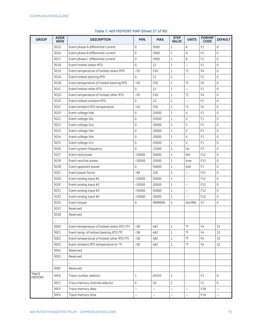
COMMUNICATIONS GUIDE
469 MOTOR MANAGEMENT RELAY – COMMUNICATIONS GUIDE 75
3015 Event phase A differential current 0 5000 1 A F1 0
3016 Event phase B differential current 0 5000 1 A F1 0
3017 Event phase C differential current 0 5000 1 A F1 0
3018 Event hottest stator RTD 0 12 1 -- F1 0
3019 Event temperature of hottest stator RTD –50 250 1 °C F4 0
301A Event hottest bearing RTD 0 12 1 -- F1 0
301B Event temperature of hottest bearing RTD –50 250 1 °C F4 0
301C Event hottest other RTD 0 12 1 -- F1 0
301D Event temperature of hottest other RTD –50 250 1 °C F4 0
301E Event hottest ambient RTD 0 12 1 -- F1 0
301F Event ambient RTD temperature –50 250 1 °C F4 0
3020 Event voltage Vab 0 20000 1 V F1 0
3021 Event voltage Vbc 0 20000 1 V F1 0
3022 Event voltage Vca 0 20000 1 V F1 0
3023 Event voltage Van 0 20000 1 V F1 0
3024 Event voltage Vbn 0 20000 1 V F1 0
3025 Event voltage Vcn 0 20000 1 V F1 0
3026 Event system frequency 0 12000 1 Hz F3 0
3027 Event real power –50000 50000 1 kW F12 0
3029 Event reactive power –50000 50000 1 kvar F12 0
302B Event apparent power 0 50000 1 kVA F1 0
302C Event power factor –99 100 1 -- F21 0
302D Event analog input #1 –50000 50000 1 -- F12 0
302F Event analog input #2 –50000 50000 1 -- F12 0
3031 Event analog input #3 –50000 50000 1 -- F12 0
3033 Event analog input #4 –50000 50000 1 -- F12 0
3035 Event torque 0 9999999 1 Nm/ftlb F2 0
3037 Reserved
3038 Reserved
… …
30E0 Event temperature of hottest stator RTD (°F) –58 482 1 °F F4 32
30E1 Event temp. of hottest bearing RTD (°F) –58 482 1 °F F4 32
30E2 Event temperature of hottest other RTD (°F) –58 482 1 °F F4 32
30E3 Event ambient RTD temperature (in °F) –58 482 1 °F F4 32
30E4 Reserved
30E5 Reserved
...
30EF Reserved
TRACEMEMORY 30F0 Trace number selector 1 65535 1 - F1 0
30F1 Trace memory channel selector 0 10 1 - F1 0
30F2 Trace memory date -- -- -- -- F18 --
30F4 Trace memory time -- -- -- -- F19 --
Table 7: 469 MEMORY MAP (Sheet 57 of 90)
GROUP ADDR(HEX) DESCRIPTION MIN. MAX. STEP
VALUE UNITS FORMATCODE DEFAULT
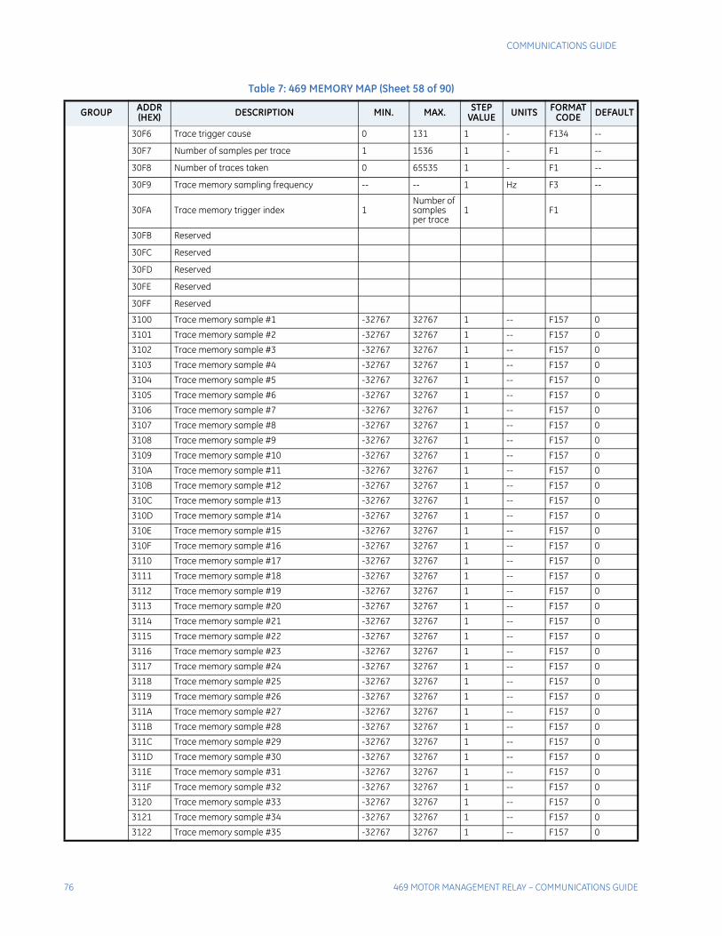
76 469 MOTOR MANAGEMENT RELAY – COMMUNICATIONS GUIDE
COMMUNICATIONS GUIDE
30F6 Trace trigger cause 0 131 1 - F134 --
30F7 Number of samples per trace 1 1536 1 - F1 --
30F8 Number of traces taken 0 65535 1 - F1 --
30F9 Trace memory sampling frequency -- -- 1 Hz F3 --
30FA Trace memory trigger index 1Number of samples per trace
1 F1
30FB Reserved
30FC Reserved
30FD Reserved
30FE Reserved
30FF Reserved
3100 Trace memory sample #1 -32767 32767 1 -- F157 0
3101 Trace memory sample #2 -32767 32767 1 -- F157 0
3102 Trace memory sample #3 -32767 32767 1 -- F157 0
3103 Trace memory sample #4 -32767 32767 1 -- F157 0
3104 Trace memory sample #5 -32767 32767 1 -- F157 0
3105 Trace memory sample #6 -32767 32767 1 -- F157 0
3106 Trace memory sample #7 -32767 32767 1 -- F157 0
3107 Trace memory sample #8 -32767 32767 1 -- F157 0
3108 Trace memory sample #9 -32767 32767 1 -- F157 0
3109 Trace memory sample #10 -32767 32767 1 -- F157 0
310A Trace memory sample #11 -32767 32767 1 -- F157 0
310B Trace memory sample #12 -32767 32767 1 -- F157 0
310C Trace memory sample #13 -32767 32767 1 -- F157 0
310D Trace memory sample #14 -32767 32767 1 -- F157 0
310E Trace memory sample #15 -32767 32767 1 -- F157 0
310F Trace memory sample #16 -32767 32767 1 -- F157 0
3110 Trace memory sample #17 -32767 32767 1 -- F157 0
3111 Trace memory sample #18 -32767 32767 1 -- F157 0
3112 Trace memory sample #19 -32767 32767 1 -- F157 0
3113 Trace memory sample #20 -32767 32767 1 -- F157 0
3114 Trace memory sample #21 -32767 32767 1 -- F157 0
3115 Trace memory sample #22 -32767 32767 1 -- F157 0
3116 Trace memory sample #23 -32767 32767 1 -- F157 0
3117 Trace memory sample #24 -32767 32767 1 -- F157 0
3118 Trace memory sample #25 -32767 32767 1 -- F157 0
3119 Trace memory sample #26 -32767 32767 1 -- F157 0
311A Trace memory sample #27 -32767 32767 1 -- F157 0
311B Trace memory sample #28 -32767 32767 1 -- F157 0
311C Trace memory sample #29 -32767 32767 1 -- F157 0
311D Trace memory sample #30 -32767 32767 1 -- F157 0
311E Trace memory sample #31 -32767 32767 1 -- F157 0
311F Trace memory sample #32 -32767 32767 1 -- F157 0
3120 Trace memory sample #33 -32767 32767 1 -- F157 0
3121 Trace memory sample #34 -32767 32767 1 -- F157 0
3122 Trace memory sample #35 -32767 32767 1 -- F157 0
Table 7: 469 MEMORY MAP (Sheet 58 of 90)
GROUP ADDR(HEX) DESCRIPTION MIN. MAX. STEP
VALUE UNITS FORMATCODE DEFAULT

COMMUNICATIONS GUIDE
469 MOTOR MANAGEMENT RELAY – COMMUNICATIONS GUIDE 77
3123 Trace memory sample #36 -32767 32767 1 -- F157 0
3124 Trace memory sample #37 -32767 32767 1 -- F157 0
3125 Trace memory sample #38 -32767 32767 1 -- F157 0
3126 Trace memory sample #39 -32767 32767 1 -- F157 0
3127 Trace memory sample #40 -32767 32767 1 -- F157 0
3128 Trace memory sample #41 -32767 32767 1 -- F157 0
3129 Trace memory sample #42 -32767 32767 1 -- F157 0
312A Trace memory sample #43 -32767 32767 1 -- F157 0
312B Trace memory sample #44 -32767 32767 1 -- F157 0
312C Trace memory sample #45 -32767 32767 1 -- F157 0
312D Trace memory sample #46 -32767 32767 1 -- F157 0
312E Trace memory sample #47 -32767 32767 1 -- F157 0
312F Trace memory sample #48 -32767 32767 1 -- F157 0
3130 Trace memory sample #49 -32767 32767 1 -- F157 0
3131 Trace memory sample #50 -32767 32767 1 -- F157 0
3132 Trace memory sample #51 -32767 32767 1 -- F157 0
3133 Trace memory sample #52 -32767 32767 1 -- F157 0
3134 Trace memory sample #53 -32767 32767 1 -- F157 0
3135 Trace memory sample #54 -32767 32767 1 -- F157 0
3136 Trace memory sample #55 -32767 32767 1 -- F157 0
3137 Trace memory sample #56 -32767 32767 1 -- F157 0
3138 Trace memory sample #57 -32767 32767 1 -- F157 0
3139 Trace memory sample #58 -32767 32767 1 -- F157 0
313A Trace memory sample #59 -32767 32767 1 -- F157 0
313B Trace memory sample #60 -32767 32767 1 -- F157 0
313C Trace memory sample #61 -32767 32767 1 -- F157 0
313D Trace memory sample #62 -32767 32767 1 -- F157 0
313E Trace memory sample #63 -32767 32767 1 -- F157 0
313F Trace memory sample #64 -32767 32767 1 -- F157 0
3140 Trace memory sample #65 -32767 32767 1 -- F157 0
3141 Trace memory sample #66 -32767 32767 1 -- F157 0
3142 Trace memory sample #67 -32767 32767 1 -- F157 0
3143 Trace memory sample #68 -32767 32767 1 -- F157 0
3144 Trace memory sample #69 -32767 32767 1 -- F157 0
3145 Trace memory sample #70 -32767 32767 1 -- F157 0
3146 Trace memory sample #71 -32767 32767 1 -- F157 0
3147 Trace memory sample #72 -32767 32767 1 -- F157 0
3148 Trace memory sample #73 -32767 32767 1 -- F157 0
3149 Trace memory sample #74 -32767 32767 1 -- F157 0
314A Trace memory sample #75 -32767 32767 1 -- F157 0
314B Trace memory sample #76 -32767 32767 1 -- F157 0
314C Trace memory sample #77 -32767 32767 1 -- F157 0
314D Trace memory sample #78 -32767 32767 1 -- F157 0
314E Trace memory sample #79 -32767 32767 1 -- F157 0
314F Trace memory sample #80 -32767 32767 1 -- F157 0
3150 Trace memory sample #81 -32767 32767 1 -- F157 0
3151 Trace memory sample #82 -32767 32767 1 -- F157 0
3152 Trace memory sample #83 -32767 32767 1 -- F157 0
Table 7: 469 MEMORY MAP (Sheet 59 of 90)
GROUP ADDR(HEX) DESCRIPTION MIN. MAX. STEP
VALUE UNITS FORMATCODE DEFAULT
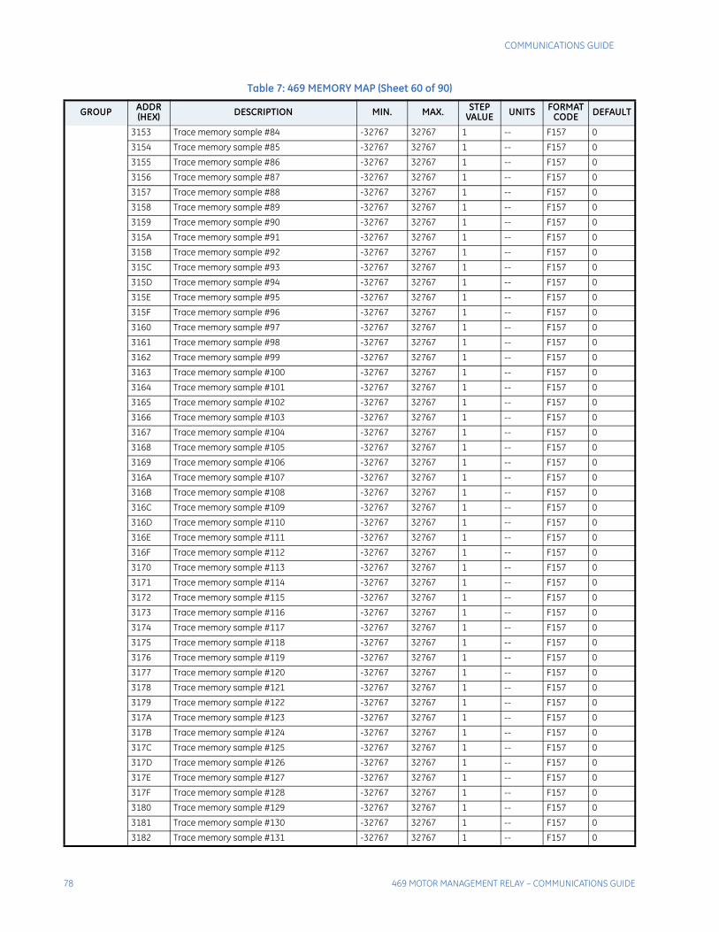
78 469 MOTOR MANAGEMENT RELAY – COMMUNICATIONS GUIDE
COMMUNICATIONS GUIDE
3153 Trace memory sample #84 -32767 32767 1 -- F157 0
3154 Trace memory sample #85 -32767 32767 1 -- F157 0
3155 Trace memory sample #86 -32767 32767 1 -- F157 0
3156 Trace memory sample #87 -32767 32767 1 -- F157 0
3157 Trace memory sample #88 -32767 32767 1 -- F157 0
3158 Trace memory sample #89 -32767 32767 1 -- F157 0
3159 Trace memory sample #90 -32767 32767 1 -- F157 0
315A Trace memory sample #91 -32767 32767 1 -- F157 0
315B Trace memory sample #92 -32767 32767 1 -- F157 0
315C Trace memory sample #93 -32767 32767 1 -- F157 0
315D Trace memory sample #94 -32767 32767 1 -- F157 0
315E Trace memory sample #95 -32767 32767 1 -- F157 0
315F Trace memory sample #96 -32767 32767 1 -- F157 0
3160 Trace memory sample #97 -32767 32767 1 -- F157 0
3161 Trace memory sample #98 -32767 32767 1 -- F157 0
3162 Trace memory sample #99 -32767 32767 1 -- F157 0
3163 Trace memory sample #100 -32767 32767 1 -- F157 0
3164 Trace memory sample #101 -32767 32767 1 -- F157 0
3165 Trace memory sample #102 -32767 32767 1 -- F157 0
3166 Trace memory sample #103 -32767 32767 1 -- F157 0
3167 Trace memory sample #104 -32767 32767 1 -- F157 0
3168 Trace memory sample #105 -32767 32767 1 -- F157 0
3169 Trace memory sample #106 -32767 32767 1 -- F157 0
316A Trace memory sample #107 -32767 32767 1 -- F157 0
316B Trace memory sample #108 -32767 32767 1 -- F157 0
316C Trace memory sample #109 -32767 32767 1 -- F157 0
316D Trace memory sample #110 -32767 32767 1 -- F157 0
316E Trace memory sample #111 -32767 32767 1 -- F157 0
316F Trace memory sample #112 -32767 32767 1 -- F157 0
3170 Trace memory sample #113 -32767 32767 1 -- F157 0
3171 Trace memory sample #114 -32767 32767 1 -- F157 0
3172 Trace memory sample #115 -32767 32767 1 -- F157 0
3173 Trace memory sample #116 -32767 32767 1 -- F157 0
3174 Trace memory sample #117 -32767 32767 1 -- F157 0
3175 Trace memory sample #118 -32767 32767 1 -- F157 0
3176 Trace memory sample #119 -32767 32767 1 -- F157 0
3177 Trace memory sample #120 -32767 32767 1 -- F157 0
3178 Trace memory sample #121 -32767 32767 1 -- F157 0
3179 Trace memory sample #122 -32767 32767 1 -- F157 0
317A Trace memory sample #123 -32767 32767 1 -- F157 0
317B Trace memory sample #124 -32767 32767 1 -- F157 0
317C Trace memory sample #125 -32767 32767 1 -- F157 0
317D Trace memory sample #126 -32767 32767 1 -- F157 0
317E Trace memory sample #127 -32767 32767 1 -- F157 0
317F Trace memory sample #128 -32767 32767 1 -- F157 0
3180 Trace memory sample #129 -32767 32767 1 -- F157 0
3181 Trace memory sample #130 -32767 32767 1 -- F157 0
3182 Trace memory sample #131 -32767 32767 1 -- F157 0
Table 7: 469 MEMORY MAP (Sheet 60 of 90)
GROUP ADDR(HEX) DESCRIPTION MIN. MAX. STEP
VALUE UNITS FORMATCODE DEFAULT

COMMUNICATIONS GUIDE
469 MOTOR MANAGEMENT RELAY – COMMUNICATIONS GUIDE 79
3183 Trace memory sample #132 -32767 32767 1 -- F157 0
3184 Trace memory sample #133 -32767 32767 1 -- F157 0
3185 Trace memory sample #134 -32767 32767 1 -- F157 0
3186 Trace memory sample #135 -32767 32767 1 -- F157 0
3187 Trace memory sample #136 -32767 32767 1 -- F157 0
3188 Trace memory sample #137 -32767 32767 1 -- F157 0
3189 Trace memory sample #138 -32767 32767 1 -- F157 0
318A Trace memory sample #139 -32767 32767 1 -- F157 0
318B Trace memory sample #140 -32767 32767 1 -- F157 0
318C Trace memory sample #141 -32767 32767 1 -- F157 0
318D Trace memory sample #142 -32767 32767 1 -- F157 0
318E Trace memory sample #143 -32767 32767 1 -- F157 0
318F Trace memory sample #144 -32767 32767 1 -- F157 0
3190 Trace memory sample #145 -32767 32767 1 -- F157 0
3191 Trace memory sample #146 -32767 32767 1 -- F157 0
3192 Trace memory sample #147 -32767 32767 1 -- F157 0
3193 Trace memory sample #148 -32767 32767 1 -- F157 0
3194 Trace memory sample #149 -32767 32767 1 -- F157 0
3195 Trace memory sample #150 -32767 32767 1 -- F157 0
3196 Trace memory sample #151 -32767 32767 1 -- F157 0
3197 Trace memory sample #152 -32767 32767 1 -- F157 0
3198 Trace memory sample #153 -32767 32767 1 -- F157 0
3199 Trace memory sample #154 -32767 32767 1 -- F157 0
319A Trace memory sample #155 -32767 32767 1 -- F157 0
319B Trace memory sample #156 -32767 32767 1 -- F157 0
319C Trace memory sample #157 -32767 32767 1 -- F157 0
319D Trace memory sample #158 -32767 32767 1 -- F157 0
319E Trace memory sample #159 -32767 32767 1 -- F157 0
319F Trace memory sample #160 -32767 32767 1 -- F157 0
31A0 Trace memory sample #161 -32767 32767 1 -- F157 0
31A1 Trace memory sample #162 -32767 32767 1 -- F157 0
31A2 Trace memory sample #163 -32767 32767 1 -- F157 0
31A3 Trace memory sample #164 -32767 32767 1 -- F157 0
31A4 Trace memory sample #165 -32767 32767 1 -- F157 0
31A5 Trace memory sample #166 -32767 32767 1 -- F157 0
31A6 Trace memory sample #167 -32767 32767 1 -- F157 0
31A7 Trace memory sample #168 -32767 32767 1 -- F157 0
31A8 Trace memory sample #169 -32767 32767 1 -- F157 0
31A9 Trace memory sample #170 -32767 32767 1 -- F157 0
31AA Trace memory sample #171 -32767 32767 1 -- F157 0
31AB Trace memory sample #172 -32767 32767 1 -- F157 0
31AC Trace memory sample #173 -32767 32767 1 -- F157 0
31AD Trace memory sample #174 -32767 32767 1 -- F157 0
31AE Trace memory sample #175 -32767 32767 1 -- F157 0
31AF Trace memory sample #176 -32767 32767 1 -- F157 0
31B0 Trace memory sample #177 -32767 32767 1 -- F157 0
31B1 Trace memory sample #178 -32767 32767 1 -- F157 0
31B2 Trace memory sample #179 -32767 32767 1 -- F157 0
Table 7: 469 MEMORY MAP (Sheet 61 of 90)
GROUP ADDR(HEX) DESCRIPTION MIN. MAX. STEP
VALUE UNITS FORMATCODE DEFAULT
80 469 MOTOR MANAGEMENT RELAY – COMMUNICATIONS GUIDE
COMMUNICATIONS GUIDE
31B3 Trace memory sample #180 -32767 32767 1 -- F157 0
31B4 Trace memory sample #181 -32767 32767 1 -- F157 0
31B5 Trace memory sample #182 -32767 32767 1 -- F157 0
31B6 Trace memory sample #183 -32767 32767 1 -- F157 0
31B7 Trace memory sample #184 -32767 32767 1 -- F157 0
31B8 Trace memory sample #185 -32767 32767 1 -- F157 0
31B9 Trace memory sample #186 -32767 32767 1 -- F157 0
31BA Trace memory sample #187 -32767 32767 1 -- F157 0
31BB Trace memory sample #188 -32767 32767 1 -- F157 0
31BC Trace memory sample #189 -32767 32767 1 -- F157 0
31BD Trace memory sample #190 -32767 32767 1 -- F157 0
31BE Trace memory sample #191 -32767 32767 1 -- F157 0
31BF Trace memory sample #192 -32767 32767 1 -- F157 0
31C0 Trace memory sample #193 -32767 32767 1 -- F157 0
31C1 Trace memory sample #194 -32767 32767 1 -- F157 0
31C2 Trace memory sample #195 -32767 32767 1 -- F157 0
31C3 Trace memory sample #196 -32767 32767 1 -- F157 0
31C4 Trace memory sample #197 -32767 32767 1 -- F157 0
31C5 Trace memory sample #198 -32767 32767 1 -- F157 0
31C6 Trace memory sample #199 -32767 32767 1 -- F157 0
31C7 Trace memory sample #200 -32767 32767 1 -- F157 0
31C8 Trace memory sample #201 -32767 32767 1 -- F157 0
31C9 Trace memory sample #202 -32767 32767 1 -- F157 0
31CA Trace memory sample #203 -32767 32767 1 -- F157 0
31CB Trace memory sample #204 -32767 32767 1 -- F157 0
31CC Trace memory sample #205 -32767 32767 1 -- F157 0
31CD Trace memory sample #206 -32767 32767 1 -- F157 0
31CE Trace memory sample #207 -32767 32767 1 -- F157 0
31CF Trace memory sample #208 -32767 32767 1 -- F157 0
31D0 Trace memory sample #209 -32767 32767 1 -- F157 0
31D1 Trace memory sample #210 -32767 32767 1 -- F157 0
31D2 Trace memory sample #211 -32767 32767 1 -- F157 0
31D3 Trace memory sample #212 -32767 32767 1 -- F157 0
31D4 Trace memory sample #213 -32767 32767 1 -- F157 0
31D5 Trace memory sample #214 -32767 32767 1 -- F157 0
31D6 Trace memory sample #215 -32767 32767 1 -- F157 0
31D7 Trace memory sample #216 -32767 32767 1 -- F157 0
31D8 Trace memory sample #217 -32767 32767 1 -- F157 0
31D9 Trace memory sample #218 -32767 32767 1 -- F157 0
31DA Trace memory sample #219 -32767 32767 1 -- F157 0
31DB Trace memory sample #220 -32767 32767 1 -- F157 0
31DC Trace memory sample #221 -32767 32767 1 -- F157 0
31DD Trace memory sample #222 -32767 32767 1 -- F157 0
31DE Trace memory sample #223 -32767 32767 1 -- F157 0
31DF Trace memory sample #224 -32767 32767 1 -- F157 0
31E0 Trace memory sample #225 -32767 32767 1 -- F157 0
31E1 Trace memory sample #226 -32767 32767 1 -- F157 0
31E2 Trace memory sample #227 -32767 32767 1 -- F157 0
Table 7: 469 MEMORY MAP (Sheet 62 of 90)
GROUP ADDR(HEX) DESCRIPTION MIN. MAX. STEP
VALUE UNITS FORMATCODE DEFAULT

COMMUNICATIONS GUIDE
469 MOTOR MANAGEMENT RELAY – COMMUNICATIONS GUIDE 81
31E3 Trace memory sample #228 -32767 32767 1 -- F157 0
31E4 Trace memory sample #229 -32767 32767 1 -- F157 0
31E5 Trace memory sample #230 -32767 32767 1 -- F157 0
31E6 Trace memory sample #231 -32767 32767 1 -- F157 0
31E7 Trace memory sample #232 -32767 32767 1 -- F157 0
31E8 Trace memory sample #233 -32767 32767 1 -- F157 0
31E9 Trace memory sample #234 -32767 32767 1 -- F157 0
31EA Trace memory sample #235 -32767 32767 1 -- F157 0
31EB Trace memory sample #236 -32767 32767 1 -- F157 0
31EC Trace memory sample #237 -32767 32767 1 -- F157 0
31ED Trace memory sample #238 -32767 32767 1 -- F157 0
31EE Trace memory sample #239 -32767 32767 1 -- F157 0
31EF Trace memory sample #240 -32767 32767 1 -- F157 0
31F0 Trace memory sample #241 -32767 32767 1 -- F157 0
31F1 Trace memory sample #242 -32767 32767 1 -- F157 0
31F2 Trace memory sample #243 -32767 32767 1 -- F157 0
31F3 Trace memory sample #244 -32767 32767 1 -- F157 0
31F4 Trace memory sample #245 -32767 32767 1 -- F157 0
31F5 Trace memory sample #246 -32767 32767 1 -- F157 0
31F6 Trace memory sample #247 -32767 32767 1 -- F157 0
31F7 Trace memory sample #248 -32767 32767 1 -- F157 0
31F8 Trace memory sample #249 -32767 32767 1 -- F157 0
31F9 Trace memory sample #250 -32767 32767 1 -- F157 0
31FA Trace memory sample #251 -32767 32767 1 -- F157 0
31FB Trace memory sample #252 -32767 32767 1 -- F157 0
31FC Trace memory sample #253 -32767 32767 1 -- F157 0
31FD Trace memory sample #254 -32767 32767 1 -- F157 0
31FE Trace memory sample #255 -32767 32767 1 -- F157 0
31FF Trace memory sample #256 -32767 32767 1 -- F157 0
3200 Trace memory sample #257 -32767 32767 1 -- F157 0
3201 Trace memory sample #258 -32767 32767 1 -- F157 0
3202 Trace memory sample #259 -32767 32767 1 -- F157 0
3203 Trace memory sample #260 -32767 32767 1 -- F157 0
3204 Trace memory sample #261 -32767 32767 1 -- F157 0
3205 Trace memory sample #262 -32767 32767 1 -- F157 0
3206 Trace memory sample #263 -32767 32767 1 -- F157 0
3207 Trace memory sample #264 -32767 32767 1 -- F157 0
3208 Trace memory sample #265 -32767 32767 1 -- F157 0
3209 Trace memory sample #266 -32767 32767 1 -- F157 0
320A Trace memory sample #267 -32767 32767 1 -- F157 0
320B Trace memory sample #268 -32767 32767 1 -- F157 0
320C Trace memory sample #269 -32767 32767 1 -- F157 0
320D Trace memory sample #270 -32767 32767 1 -- F157 0
320E Trace memory sample #271 -32767 32767 1 -- F157 0
320F Trace memory sample #272 -32767 32767 1 -- F157 0
3210 Trace memory sample #273 -32767 32767 1 -- F157 0
3211 Trace memory sample #274 -32767 32767 1 -- F157 0
3212 Trace memory sample #275 -32767 32767 1 -- F157 0
Table 7: 469 MEMORY MAP (Sheet 63 of 90)
GROUP ADDR(HEX) DESCRIPTION MIN. MAX. STEP
VALUE UNITS FORMATCODE DEFAULT
82 469 MOTOR MANAGEMENT RELAY – COMMUNICATIONS GUIDE
COMMUNICATIONS GUIDE
3213 Trace memory sample #276 -32767 32767 1 -- F157 0
3214 Trace memory sample #277 -32767 32767 1 -- F157 0
3215 Trace memory sample #278 -32767 32767 1 -- F157 0
3216 Trace memory sample #279 -32767 32767 1 -- F157 0
3217 Trace memory sample #280 -32767 32767 1 -- F157 0
3218 Trace memory sample #281 -32767 32767 1 -- F157 0
3219 Trace memory sample #282 -32767 32767 1 -- F157 0
321A Trace memory sample #283 -32767 32767 1 -- F157 0
321B Trace memory sample #284 -32767 32767 1 -- F157 0
321C Trace memory sample #285 -32767 32767 1 -- F157 0
321D Trace memory sample #286 -32767 32767 1 -- F157 0
321E Trace memory sample #287 -32767 32767 1 -- F157 0
321F Trace memory sample #288 -32767 32767 1 -- F157 0
3220 Trace memory sample #289 -32767 32767 1 -- F157 0
3221 Trace memory sample #290 -32767 32767 1 -- F157 0
3222 Trace memory sample #291 -32767 32767 1 -- F157 0
3223 Trace memory sample #292 -32767 32767 1 -- F157 0
3224 Trace memory sample #293 -32767 32767 1 -- F157 0
3225 Trace memory sample #294 -32767 32767 1 -- F157 0
3226 Trace memory sample #295 -32767 32767 1 -- F157 0
3227 Trace memory sample #296 -32767 32767 1 -- F157 0
3228 Trace memory sample #297 -32767 32767 1 -- F157 0
3229 Trace memory sample #298 -32767 32767 1 -- F157 0
322A Trace memory sample #299 -32767 32767 1 -- F157 0
322B Trace memory sample #300 -32767 32767 1 -- F157 0
322C Trace memory sample #301 -32767 32767 1 -- F157 0
322D Trace memory sample #302 -32767 32767 1 -- F157 0
322E Trace memory sample #303 -32767 32767 1 -- F157 0
322F Trace memory sample #304 -32767 32767 1 -- F157 0
3230 Trace memory sample #305 -32767 32767 1 -- F157 0
3231 Trace memory sample #306 -32767 32767 1 -- F157 0
3232 Trace memory sample #307 -32767 32767 1 -- F157 0
3233 Trace memory sample #308 -32767 32767 1 -- F157 0
3234 Trace memory sample #309 -32767 32767 1 -- F157 0
3235 Trace memory sample #310 -32767 32767 1 -- F157 0
3236 Trace memory sample #311 -32767 32767 1 -- F157 0
3237 Trace memory sample #312 -32767 32767 1 -- F157 0
3238 Trace memory sample #313 -32767 32767 1 -- F157 0
3239 Trace memory sample #314 -32767 32767 1 -- F157 0
323A Trace memory sample #315 -32767 32767 1 -- F157 0
323B Trace memory sample #316 -32767 32767 1 -- F157 0
323C Trace memory sample #317 -32767 32767 1 -- F157 0
323D Trace memory sample #318 -32767 32767 1 -- F157 0
323E Trace memory sample #319 -32767 32767 1 -- F157 0
323F Trace memory sample #320 -32767 32767 1 -- F157 0
3240 Trace memory sample #321 -32767 32767 1 -- F157 0
3241 Trace memory sample #322 -32767 32767 1 -- F157 0
3242 Trace memory sample #323 -32767 32767 1 -- F157 0
Table 7: 469 MEMORY MAP (Sheet 64 of 90)
GROUP ADDR(HEX) DESCRIPTION MIN. MAX. STEP
VALUE UNITS FORMATCODE DEFAULT

COMMUNICATIONS GUIDE
469 MOTOR MANAGEMENT RELAY – COMMUNICATIONS GUIDE 83
3243 Trace memory sample #324 -32767 32767 1 -- F157 0
3244 Trace memory sample #325 -32767 32767 1 -- F157 0
3245 Trace memory sample #326 -32767 32767 1 -- F157 0
3246 Trace memory sample #327 -32767 32767 1 -- F157 0
3247 Trace memory sample #328 -32767 32767 1 -- F157 0
3248 Trace memory sample #329 -32767 32767 1 -- F157 0
3249 Trace memory sample #330 -32767 32767 1 -- F157 0
324A Trace memory sample #331 -32767 32767 1 -- F157 0
324B Trace memory sample #332 -32767 32767 1 -- F157 0
324C Trace memory sample #333 -32767 32767 1 -- F157 0
324D Trace memory sample #334 -32767 32767 1 -- F157 0
324E Trace memory sample #335 -32767 32767 1 -- F157 0
324F Trace memory sample #336 -32767 32767 1 -- F157 0
3250 Trace memory sample #337 -32767 32767 1 -- F157 0
3251 Trace memory sample #338 -32767 32767 1 -- F157 0
3252 Trace memory sample #339 -32767 32767 1 -- F157 0
3253 Trace memory sample #340 -32767 32767 1 -- F157 0
3254 Trace memory sample #341 -32767 32767 1 -- F157 0
3255 Trace memory sample #342 -32767 32767 1 -- F157 0
3256 Trace memory sample #343 -32767 32767 1 -- F157 0
3257 Trace memory sample #344 -32767 32767 1 -- F157 0
3258 Trace memory sample #345 -32767 32767 1 -- F157 0
3259 Trace memory sample #346 -32767 32767 1 -- F157 0
325A Trace memory sample #347 -32767 32767 1 -- F157 0
325B Trace memory sample #348 -32767 32767 1 -- F157 0
325C Trace memory sample #349 -32767 32767 1 -- F157 0
325D Trace memory sample #350 -32767 32767 1 -- F157 0
325E Trace memory sample #351 -32767 32767 1 -- F157 0
325F Trace memory sample #352 -32767 32767 1 -- F157 0
3260 Trace memory sample #353 -32767 32767 1 -- F157 0
3261 Trace memory sample #354 -32767 32767 1 -- F157 0
3262 Trace memory sample #355 -32767 32767 1 -- F157 0
3263 Trace memory sample #356 -32767 32767 1 -- F157 0
3264 Trace memory sample #357 -32767 32767 1 -- F157 0
3265 Trace memory sample #358 -32767 32767 1 -- F157 0
3266 Trace memory sample #359 -32767 32767 1 -- F157 0
3267 Trace memory sample #360 -32767 32767 1 -- F157 0
3268 Trace memory sample #361 -32767 32767 1 -- F157 0
3269 Trace memory sample #362 -32767 32767 1 -- F157 0
326A Trace memory sample #363 -32767 32767 1 -- F157 0
326B Trace memory sample #364 -32767 32767 1 -- F157 0
326C Trace memory sample #365 -32767 32767 1 -- F157 0
326D Trace memory sample #366 -32767 32767 1 -- F157 0
326E Trace memory sample #367 -32767 32767 1 -- F157 0
326F Trace memory sample #368 -32767 32767 1 -- F157 0
3270 Trace memory sample #369 -32767 32767 1 -- F157 0
3271 Trace memory sample #370 -32767 32767 1 -- F157 0
3272 Trace memory sample #371 -32767 32767 1 -- F157 0
Table 7: 469 MEMORY MAP (Sheet 65 of 90)
GROUP ADDR(HEX) DESCRIPTION MIN. MAX. STEP
VALUE UNITS FORMATCODE DEFAULT
84 469 MOTOR MANAGEMENT RELAY – COMMUNICATIONS GUIDE
COMMUNICATIONS GUIDE
3273 Trace memory sample #372 -32767 32767 1 -- F157 0
3274 Trace memory sample #373 -32767 32767 1 -- F157 0
3275 Trace memory sample #374 -32767 32767 1 -- F157 0
3276 Trace memory sample #375 -32767 32767 1 -- F157 0
3277 Trace memory sample #376 -32767 32767 1 -- F157 0
3278 Trace memory sample #377 -32767 32767 1 -- F157 0
3279 Trace memory sample #378 -32767 32767 1 -- F157 0
327A Trace memory sample #379 -32767 32767 1 -- F157 0
327B Trace memory sample #380 -32767 32767 1 -- F157 0
327C Trace memory sample #381 -32767 32767 1 -- F157 0
327D Trace memory sample #382 -32767 32767 1 -- F157 0
327E Trace memory sample #383 -32767 32767 1 -- F157 0
327F Trace memory sample #384 -32767 32767 1 -- F157 0
3280 Trace memory sample #385 -32767 32767 1 -- F157 0
3281 Trace memory sample #386 -32767 32767 1 -- F157 0
3282 Trace memory sample #387 -32767 32767 1 -- F157 0
3283 Trace memory sample #388 -32767 32767 1 -- F157 0
3284 Trace memory sample #389 -32767 32767 1 -- F157 0
3285 Trace memory sample #390 -32767 32767 1 -- F157 0
3286 Trace memory sample #391 -32767 32767 1 -- F157 0
3287 Trace memory sample #392 -32767 32767 1 -- F157 0
3288 Trace memory sample #393 -32767 32767 1 -- F157 0
3289 Trace memory sample #394 -32767 32767 1 -- F157 0
328A Trace memory sample #395 -32767 32767 1 -- F157 0
328B Trace memory sample #396 -32767 32767 1 -- F157 0
328C Trace memory sample #397 -32767 32767 1 -- F157 0
328D Trace memory sample #398 -32767 32767 1 -- F157 0
328E Trace memory sample #399 -32767 32767 1 -- F157 0
328F Trace memory sample #400 -32767 32767 1 -- F157 0
3290 Trace memory sample #401 -32767 32767 1 -- F157 0
3291 Trace memory sample #402 -32767 32767 1 -- F157 0
3292 Trace memory sample #403 -32767 32767 1 -- F157 0
3293 Trace memory sample #404 -32767 32767 1 -- F157 0
3294 Trace memory sample #405 -32767 32767 1 -- F157 0
3295 Trace memory sample #406 -32767 32767 1 -- F157 0
3296 Trace memory sample #407 -32767 32767 1 -- F157 0
3297 Trace memory sample #408 -32767 32767 1 -- F157 0
3298 Trace memory sample #409 -32767 32767 1 -- F157 0
3299 Trace memory sample #410 -32767 32767 1 -- F157 0
329A Trace memory sample #411 -32767 32767 1 -- F157 0
329B Trace memory sample #412 -32767 32767 1 -- F157 0
329C Trace memory sample #413 -32767 32767 1 -- F157 0
329D Trace memory sample #414 -32767 32767 1 -- F157 0
329E Trace memory sample #415 -32767 32767 1 -- F157 0
329F Trace memory sample #416 -32767 32767 1 -- F157 0
32A0 Trace memory sample #417 -32767 32767 1 -- F157 0
32A1 Trace memory sample #418 -32767 32767 1 -- F157 0
32A2 Trace memory sample #419 -32767 32767 1 -- F157 0
Table 7: 469 MEMORY MAP (Sheet 66 of 90)
GROUP ADDR(HEX) DESCRIPTION MIN. MAX. STEP
VALUE UNITS FORMATCODE DEFAULT

COMMUNICATIONS GUIDE
469 MOTOR MANAGEMENT RELAY – COMMUNICATIONS GUIDE 85
32A3 Trace memory sample #420 -32767 32767 1 -- F157 0
32A4 Trace memory sample #421 -32767 32767 1 -- F157 0
32A5 Trace memory sample #422 -32767 32767 1 -- F157 0
32A6 Trace memory sample #423 -32767 32767 1 -- F157 0
32A7 Trace memory sample #424 -32767 32767 1 -- F157 0
32A8 Trace memory sample #425 -32767 32767 1 -- F157 0
32A9 Trace memory sample #426 -32767 32767 1 -- F157 0
32AA Trace memory sample #427 -32767 32767 1 -- F157 0
32AB Trace memory sample #428 -32767 32767 1 -- F157 0
32AC Trace memory sample #429 -32767 32767 1 -- F157 0
32AD Trace memory sample #430 -32767 32767 1 -- F157 0
32AE Trace memory sample #431 -32767 32767 1 -- F157 0
32AF Trace memory sample #432 -32767 32767 1 -- F157 0
32B0 Trace memory sample #433 -32767 32767 1 -- F157 0
32B1 Trace memory sample #434 -32767 32767 1 -- F157 0
32B2 Trace memory sample #435 -32767 32767 1 -- F157 0
32B3 Trace memory sample #436 -32767 32767 1 -- F157 0
32B4 Trace memory sample #437 -32767 32767 1 -- F157 0
32B5 Trace memory sample #438 -32767 32767 1 -- F157 0
32B6 Trace memory sample #439 -32767 32767 1 -- F157 0
32B7 Trace memory sample #440 -32767 32767 1 -- F157 0
32B8 Trace memory sample #441 -32767 32767 1 -- F157 0
32B9 Trace memory sample #442 -32767 32767 1 -- F157 0
32BA Trace memory sample #443 -32767 32767 1 -- F157 0
32BB Trace memory sample #444 -32767 32767 1 -- F157 0
32BC Trace memory sample #445 -32767 32767 1 -- F157 0
32BD Trace memory sample #446 -32767 32767 1 -- F157 0
32BE Trace memory sample #447 -32767 32767 1 -- F157 0
32BF Trace memory sample #448 -32767 32767 1 -- F157 0
32C0 Trace memory sample #449 -32767 32767 1 -- F157 0
32C1 Trace memory sample #450 -32767 32767 1 -- F157 0
32C2 Trace memory sample #451 -32767 32767 1 -- F157 0
32C3 Trace memory sample #452 -32767 32767 1 -- F157 0
32C4 Trace memory sample #453 -32767 32767 1 -- F157 0
32C5 Trace memory sample #454 -32767 32767 1 -- F157 0
32C6 Trace memory sample #455 -32767 32767 1 -- F157 0
32C7 Trace memory sample #456 -32767 32767 1 -- F157 0
32C8 Trace memory sample #457 -32767 32767 1 -- F157 0
32C9 Trace memory sample #458 -32767 32767 1 -- F157 0
32CA Trace memory sample #459 -32767 32767 1 -- F157 0
32CB Trace memory sample #460 -32767 32767 1 -- F157 0
32CC Trace memory sample #461 -32767 32767 1 -- F157 0
32CD Trace memory sample #462 -32767 32767 1 -- F157 0
32CE Trace memory sample #463 -32767 32767 1 -- F157 0
32CF Trace memory sample #464 -32767 32767 1 -- F157 0
32D0 Trace memory sample #465 -32767 32767 1 -- F157 0
32D1 Trace memory sample #466 -32767 32767 1 -- F157 0
32D2 Trace memory sample #467 -32767 32767 1 -- F157 0
Table 7: 469 MEMORY MAP (Sheet 67 of 90)
GROUP ADDR(HEX) DESCRIPTION MIN. MAX. STEP
VALUE UNITS FORMATCODE DEFAULT
86 469 MOTOR MANAGEMENT RELAY – COMMUNICATIONS GUIDE
COMMUNICATIONS GUIDE
32D3 Trace memory sample #468 -32767 32767 1 -- F157 0
32D4 Trace memory sample #469 -32767 32767 1 -- F157 0
32D5 Trace memory sample #470 -32767 32767 1 -- F157 0
32D6 Trace memory sample #471 -32767 32767 1 -- F157 0
32D7 Trace memory sample #472 -32767 32767 1 -- F157 0
32D8 Trace memory sample #473 -32767 32767 1 -- F157 0
32D9 Trace memory sample #474 -32767 32767 1 -- F157 0
32DA Trace memory sample #475 -32767 32767 1 -- F157 0
32DB Trace memory sample #476 -32767 32767 1 -- F157 0
32DC Trace memory sample #477 -32767 32767 1 -- F157 0
32DD Trace memory sample #478 -32767 32767 1 -- F157 0
32DE Trace memory sample #479 -32767 32767 1 -- F157 0
32DF Trace memory sample #480 -32767 32767 1 -- F157 0
32E0 Trace memory sample #481 -32767 32767 1 -- F157 0
32E1 Trace memory sample #482 -32767 32767 1 -- F157 0
32E2 Trace memory sample #483 -32767 32767 1 -- F157 0
32E3 Trace memory sample #484 -32767 32767 1 -- F157 0
32E4 Trace memory sample #485 -32767 32767 1 -- F157 0
32E5 Trace memory sample #486 -32767 32767 1 -- F157 0
32E6 Trace memory sample #487 -32767 32767 1 -- F157 0
32E7 Trace memory sample #488 -32767 32767 1 -- F157 0
32E8 Trace memory sample #489 -32767 32767 1 -- F157 0
32E9 Trace memory sample #490 -32767 32767 1 -- F157 0
32EA Trace memory sample #491 -32767 32767 1 -- F157 0
32EB Trace memory sample #492 -32767 32767 1 -- F157 0
32EC Trace memory sample #493 -32767 32767 1 -- F157 0
32ED Trace memory sample #494 -32767 32767 1 -- F157 0
32EE Trace memory sample #495 -32767 32767 1 -- F157 0
32EF Trace memory sample #496 -32767 32767 1 -- F157 0
32F0 Trace memory sample #497 -32767 32767 1 -- F157 0
32F1 Trace memory sample #498 -32767 32767 1 -- F157 0
32F2 Trace memory sample #499 -32767 32767 1 -- F157 0
32F3 Trace memory sample #500 -32767 32767 1 -- F157 0
32F4 Trace memory sample #501 -32767 32767 1 -- F157 0
32F5 Trace memory sample #502 -32767 32767 1 -- F157 0
32F6 Trace memory sample #503 -32767 32767 1 -- F157 0
32F7 Trace memory sample #504 -32767 32767 1 -- F157 0
32F8 Trace memory sample #505 -32767 32767 1 -- F157 0
32F9 Trace memory sample #506 -32767 32767 1 -- F157 0
32FA Trace memory sample #507 -32767 32767 1 -- F157 0
32FB Trace memory sample #508 -32767 32767 1 -- F157 0
32FC Trace memory sample #509 -32767 32767 1 -- F157 0
32FD Trace memory sample #510 -32767 32767 1 -- F157 0
32FE Trace memory sample #511 -32767 32767 1 -- F157 0
32FF Trace memory sample #512 -32767 32767 1 -- F157 0
3300 Trace memory sample #513 -32767 32767 1 -- F157 0
3301 Trace memory sample #514 -32767 32767 1 -- F157 0
3302 Trace memory sample #515 -32767 32767 1 -- F157 0
Table 7: 469 MEMORY MAP (Sheet 68 of 90)
GROUP ADDR(HEX) DESCRIPTION MIN. MAX. STEP
VALUE UNITS FORMATCODE DEFAULT

COMMUNICATIONS GUIDE
469 MOTOR MANAGEMENT RELAY – COMMUNICATIONS GUIDE 87
3303 Trace memory sample #516 -32767 32767 1 -- F157 0
3304 Trace memory sample #517 -32767 32767 1 -- F157 0
3305 Trace memory sample #518 -32767 32767 1 -- F157 0
3306 Trace memory sample #519 -32767 32767 1 -- F157 0
3307 Trace memory sample #520 -32767 32767 1 -- F157 0
3308 Trace memory sample #521 -32767 32767 1 -- F157 0
3309 Trace memory sample #522 -32767 32767 1 -- F157 0
330A Trace memory sample #523 -32767 32767 1 -- F157 0
330B Trace memory sample #524 -32767 32767 1 -- F157 0
330C Trace memory sample #525 -32767 32767 1 -- F157 0
330D Trace memory sample #526 -32767 32767 1 -- F157 0
330E Trace memory sample #527 -32767 32767 1 -- F157 0
330F Trace memory sample #528 -32767 32767 1 -- F157 0
3310 Trace memory sample #529 -32767 32767 1 -- F157 0
3311 Trace memory sample #530 -32767 32767 1 -- F157 0
3312 Trace memory sample #531 -32767 32767 1 -- F157 0
3313 Trace memory sample #532 -32767 32767 1 -- F157 0
3314 Trace memory sample #533 -32767 32767 1 -- F157 0
3315 Trace memory sample #534 -32767 32767 1 -- F157 0
3316 Trace memory sample #535 -32767 32767 1 -- F157 0
3317 Trace memory sample #536 -32767 32767 1 -- F157 0
3318 Trace memory sample #537 -32767 32767 1 -- F157 0
3319 Trace memory sample #538 -32767 32767 1 -- F157 0
331A Trace memory sample #539 -32767 32767 1 -- F157 0
331B Trace memory sample #540 -32767 32767 1 -- F157 0
331C Trace memory sample #541 -32767 32767 1 -- F157 0
331D Trace memory sample #542 -32767 32767 1 -- F157 0
331E Trace memory sample #543 -32767 32767 1 -- F157 0
331F Trace memory sample #544 -32767 32767 1 -- F157 0
3320 Trace memory sample #545 -32767 32767 1 -- F157 0
3321 Trace memory sample #546 -32767 32767 1 -- F157 0
3322 Trace memory sample #547 -32767 32767 1 -- F157 0
3323 Trace memory sample #548 -32767 32767 1 -- F157 0
3324 Trace memory sample #549 -32767 32767 1 -- F157 0
3325 Trace memory sample #550 -32767 32767 1 -- F157 0
3326 Trace memory sample #551 -32767 32767 1 -- F157 0
3327 Trace memory sample #552 -32767 32767 1 -- F157 0
3328 Trace memory sample #553 -32767 32767 1 -- F157 0
3329 Trace memory sample #554 -32767 32767 1 -- F157 0
332A Trace memory sample #555 -32767 32767 1 -- F157 0
332B Trace memory sample #556 -32767 32767 1 -- F157 0
332C Trace memory sample #557 -32767 32767 1 -- F157 0
332D Trace memory sample #558 -32767 32767 1 -- F157 0
332E Trace memory sample #559 -32767 32767 1 -- F157 0
332F Trace memory sample #560 -32767 32767 1 -- F157 0
3330 Trace memory sample #561 -32767 32767 1 -- F157 0
3331 Trace memory sample #562 -32767 32767 1 -- F157 0
3332 Trace memory sample #563 -32767 32767 1 -- F157 0
Table 7: 469 MEMORY MAP (Sheet 69 of 90)
GROUP ADDR(HEX) DESCRIPTION MIN. MAX. STEP
VALUE UNITS FORMATCODE DEFAULT

88 469 MOTOR MANAGEMENT RELAY – COMMUNICATIONS GUIDE
COMMUNICATIONS GUIDE
3333 Trace memory sample #564 -32767 32767 1 -- F157 0
3334 Trace memory sample #565 -32767 32767 1 -- F157 0
3335 Trace memory sample #566 -32767 32767 1 -- F157 0
3336 Trace memory sample #567 -32767 32767 1 -- F157 0
3337 Trace memory sample #568 -32767 32767 1 -- F157 0
3338 Trace memory sample #569 -32767 32767 1 -- F157 0
3339 Trace memory sample #570 -32767 32767 1 -- F157 0
333A Trace memory sample #571 -32767 32767 1 -- F157 0
333B Trace memory sample #572 -32767 32767 1 -- F157 0
333C Trace memory sample #573 -32767 32767 1 -- F157 0
333D Trace memory sample #574 -32767 32767 1 -- F157 0
333E Trace memory sample #575 -32767 32767 1 -- F157 0
333F Trace memory sample #576 -32767 32767 1 -- F157 0
3340 Trace memory sample #577 -32767 32767 1 -- F157 0
3341 Trace memory sample #578 -32767 32767 1 -- F157 0
3342 Trace memory sample #579 -32767 32767 1 -- F157 0
3343 Trace memory sample #580 -32767 32767 1 -- F157 0
3344 Trace memory sample #581 -32767 32767 1 -- F157 0
3345 Trace memory sample #582 -32767 32767 1 -- F157 0
3346 Trace memory sample #583 -32767 32767 1 -- F157 0
3347 Trace memory sample #584 -32767 32767 1 -- F157 0
3348 Trace memory sample #585 -32767 32767 1 -- F157 0
3349 Trace memory sample #586 -32767 32767 1 -- F157 0
334A Trace memory sample #587 -32767 32767 1 -- F157 0
334B Trace memory sample #588 -32767 32767 1 -- F157 0
334C Trace memory sample #589 -32767 32767 1 -- F157 0
334D Trace memory sample #590 -32767 32767 1 -- F157 0
334E Trace memory sample #591 -32767 32767 1 -- F157 0
334F Trace memory sample #592 -32767 32767 1 -- F157 0
3350 Trace memory sample #593 -32767 32767 1 -- F157 0
3351 Trace memory sample #594 -32767 32767 1 -- F157 0
3352 Trace memory sample #595 -32767 32767 1 -- F157 0
3353 Trace memory sample #596 -32767 32767 1 -- F157 0
3354 Trace memory sample #597 -32767 32767 1 -- F157 0
3355 Trace memory sample #598 -32767 32767 1 -- F157 0
3356 Trace memory sample #599 -32767 32767 1 -- F157 0
3357 Trace memory sample #600 -32767 32767 1 -- F157 0
3358 Trace memory sample #601 -32767 32767 1 -- F157 0
3359 Trace memory sample #602 -32767 32767 1 -- F157 0
335A Trace memory sample #603 -32767 32767 1 -- F157 0
335B Trace memory sample #604 -32767 32767 1 -- F157 0
335C Trace memory sample #605 -32767 32767 1 -- F157 0
335D Trace memory sample #606 -32767 32767 1 -- F157 0
335E Trace memory sample #607 -32767 32767 1 -- F157 0
335F Trace memory sample #608 -32767 32767 1 -- F157 0
3360 Trace memory sample #609 -32767 32767 1 -- F157 0
3361 Trace memory sample #610 -32767 32767 1 -- F157 0
3362 Trace memory sample #611 -32767 32767 1 -- F157 0
Table 7: 469 MEMORY MAP (Sheet 70 of 90)
GROUP ADDR(HEX) DESCRIPTION MIN. MAX. STEP
VALUE UNITS FORMATCODE DEFAULT
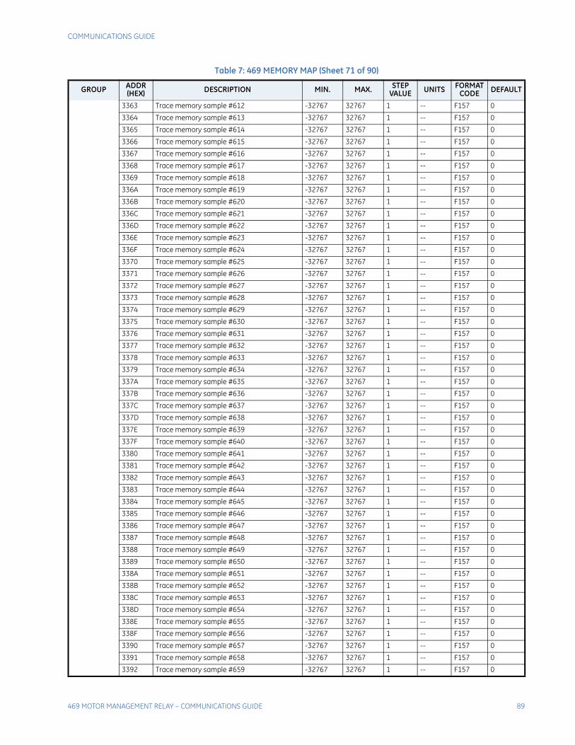
COMMUNICATIONS GUIDE
469 MOTOR MANAGEMENT RELAY – COMMUNICATIONS GUIDE 89
3363 Trace memory sample #612 -32767 32767 1 -- F157 0
3364 Trace memory sample #613 -32767 32767 1 -- F157 0
3365 Trace memory sample #614 -32767 32767 1 -- F157 0
3366 Trace memory sample #615 -32767 32767 1 -- F157 0
3367 Trace memory sample #616 -32767 32767 1 -- F157 0
3368 Trace memory sample #617 -32767 32767 1 -- F157 0
3369 Trace memory sample #618 -32767 32767 1 -- F157 0
336A Trace memory sample #619 -32767 32767 1 -- F157 0
336B Trace memory sample #620 -32767 32767 1 -- F157 0
336C Trace memory sample #621 -32767 32767 1 -- F157 0
336D Trace memory sample #622 -32767 32767 1 -- F157 0
336E Trace memory sample #623 -32767 32767 1 -- F157 0
336F Trace memory sample #624 -32767 32767 1 -- F157 0
3370 Trace memory sample #625 -32767 32767 1 -- F157 0
3371 Trace memory sample #626 -32767 32767 1 -- F157 0
3372 Trace memory sample #627 -32767 32767 1 -- F157 0
3373 Trace memory sample #628 -32767 32767 1 -- F157 0
3374 Trace memory sample #629 -32767 32767 1 -- F157 0
3375 Trace memory sample #630 -32767 32767 1 -- F157 0
3376 Trace memory sample #631 -32767 32767 1 -- F157 0
3377 Trace memory sample #632 -32767 32767 1 -- F157 0
3378 Trace memory sample #633 -32767 32767 1 -- F157 0
3379 Trace memory sample #634 -32767 32767 1 -- F157 0
337A Trace memory sample #635 -32767 32767 1 -- F157 0
337B Trace memory sample #636 -32767 32767 1 -- F157 0
337C Trace memory sample #637 -32767 32767 1 -- F157 0
337D Trace memory sample #638 -32767 32767 1 -- F157 0
337E Trace memory sample #639 -32767 32767 1 -- F157 0
337F Trace memory sample #640 -32767 32767 1 -- F157 0
3380 Trace memory sample #641 -32767 32767 1 -- F157 0
3381 Trace memory sample #642 -32767 32767 1 -- F157 0
3382 Trace memory sample #643 -32767 32767 1 -- F157 0
3383 Trace memory sample #644 -32767 32767 1 -- F157 0
3384 Trace memory sample #645 -32767 32767 1 -- F157 0
3385 Trace memory sample #646 -32767 32767 1 -- F157 0
3386 Trace memory sample #647 -32767 32767 1 -- F157 0
3387 Trace memory sample #648 -32767 32767 1 -- F157 0
3388 Trace memory sample #649 -32767 32767 1 -- F157 0
3389 Trace memory sample #650 -32767 32767 1 -- F157 0
338A Trace memory sample #651 -32767 32767 1 -- F157 0
338B Trace memory sample #652 -32767 32767 1 -- F157 0
338C Trace memory sample #653 -32767 32767 1 -- F157 0
338D Trace memory sample #654 -32767 32767 1 -- F157 0
338E Trace memory sample #655 -32767 32767 1 -- F157 0
338F Trace memory sample #656 -32767 32767 1 -- F157 0
3390 Trace memory sample #657 -32767 32767 1 -- F157 0
3391 Trace memory sample #658 -32767 32767 1 -- F157 0
3392 Trace memory sample #659 -32767 32767 1 -- F157 0
Table 7: 469 MEMORY MAP (Sheet 71 of 90)
GROUP ADDR(HEX) DESCRIPTION MIN. MAX. STEP
VALUE UNITS FORMATCODE DEFAULT
90 469 MOTOR MANAGEMENT RELAY – COMMUNICATIONS GUIDE
COMMUNICATIONS GUIDE
3393 Trace memory sample #660 -32767 32767 1 -- F157 0
3394 Trace memory sample #661 -32767 32767 1 -- F157 0
3395 Trace memory sample #662 -32767 32767 1 -- F157 0
3396 Trace memory sample #663 -32767 32767 1 -- F157 0
3397 Trace memory sample #664 -32767 32767 1 -- F157 0
3398 Trace memory sample #665 -32767 32767 1 -- F157 0
3399 Trace memory sample #666 -32767 32767 1 -- F157 0
339A Trace memory sample #667 -32767 32767 1 -- F157 0
339B Trace memory sample #668 -32767 32767 1 -- F157 0
339C Trace memory sample #669 -32767 32767 1 -- F157 0
339D Trace memory sample #670 -32767 32767 1 -- F157 0
339E Trace memory sample #671 -32767 32767 1 -- F157 0
339F Trace memory sample #672 -32767 32767 1 -- F157 0
33A0 Trace memory sample #673 -32767 32767 1 -- F157 0
33A1 Trace memory sample #674 -32767 32767 1 -- F157 0
33A2 Trace memory sample #675 -32767 32767 1 -- F157 0
33A3 Trace memory sample #676 -32767 32767 1 -- F157 0
33A4 Trace memory sample #677 -32767 32767 1 -- F157 0
33A5 Trace memory sample #678 -32767 32767 1 -- F157 0
33A6 Trace memory sample #679 -32767 32767 1 -- F157 0
33A7 Trace memory sample #680 -32767 32767 1 -- F157 0
33A8 Trace memory sample #681 -32767 32767 1 -- F157 0
33A9 Trace memory sample #682 -32767 32767 1 -- F157 0
33AA Trace memory sample #683 -32767 32767 1 -- F157 0
33AB Trace memory sample #684 -32767 32767 1 -- F157 0
33AC Trace memory sample #685 -32767 32767 1 -- F157 0
33AD Trace memory sample #686 -32767 32767 1 -- F157 0
33AE Trace memory sample #687 -32767 32767 1 -- F157 0
33AF Trace memory sample #688 -32767 32767 1 -- F157 0
33B0 Trace memory sample #689 -32767 32767 1 -- F157 0
33B1 Trace memory sample #690 -32767 32767 1 -- F157 0
33B2 Trace memory sample #691 -32767 32767 1 -- F157 0
33B3 Trace memory sample #692 -32767 32767 1 -- F157 0
33B4 Trace memory sample #693 -32767 32767 1 -- F157 0
33B5 Trace memory sample #694 -32767 32767 1 -- F157 0
33B6 Trace memory sample #695 -32767 32767 1 -- F157 0
33B7 Trace memory sample #696 -32767 32767 1 -- F157 0
33B8 Trace memory sample #697 -32767 32767 1 -- F157 0
33B9 Trace memory sample #698 -32767 32767 1 -- F157 0
33BA Trace memory sample #699 -32767 32767 1 -- F157 0
33BB Trace memory sample #700 -32767 32767 1 -- F157 0
33BC Trace memory sample #701 -32767 32767 1 -- F157 0
33BD Trace memory sample #702 -32767 32767 1 -- F157 0
33BE Trace memory sample #703 -32767 32767 1 -- F157 0
33BF Trace memory sample #704 -32767 32767 1 -- F157 0
33C0 Trace memory sample #705 -32767 32767 1 -- F157 0
33C1 Trace memory sample #706 -32767 32767 1 -- F157 0
33C2 Trace memory sample #707 -32767 32767 1 -- F157 0
Table 7: 469 MEMORY MAP (Sheet 72 of 90)
GROUP ADDR(HEX) DESCRIPTION MIN. MAX. STEP
VALUE UNITS FORMATCODE DEFAULT

COMMUNICATIONS GUIDE
469 MOTOR MANAGEMENT RELAY – COMMUNICATIONS GUIDE 91
33C3 Trace memory sample #708 -32767 32767 1 -- F157 0
33C4 Trace memory sample #709 -32767 32767 1 -- F157 0
33C5 Trace memory sample #710 -32767 32767 1 -- F157 0
33C6 Trace memory sample #711 -32767 32767 1 -- F157 0
33C7 Trace memory sample #712 -32767 32767 1 -- F157 0
33C8 Trace memory sample #713 -32767 32767 1 -- F157 0
33C9 Trace memory sample #714 -32767 32767 1 -- F157 0
33CA Trace memory sample #715 -32767 32767 1 -- F157 0
33CB Trace memory sample #716 -32767 32767 1 -- F157 0
33CC Trace memory sample #717 -32767 32767 1 -- F157 0
33CD Trace memory sample #718 -32767 32767 1 -- F157 0
33CE Trace memory sample #719 -32767 32767 1 -- F157 0
33CF Trace memory sample #720 -32767 32767 1 -- F157 0
33D0 Trace memory sample #721 -32767 32767 1 -- F157 0
33D1 Trace memory sample #722 -32767 32767 1 -- F157 0
33D2 Trace memory sample #723 -32767 32767 1 -- F157 0
33D3 Trace memory sample #724 -32767 32767 1 -- F157 0
33D4 Trace memory sample #725 -32767 32767 1 -- F157 0
33D5 Trace memory sample #726 -32767 32767 1 -- F157 0
33D6 Trace memory sample #727 -32767 32767 1 -- F157 0
33D7 Trace memory sample #728 -32767 32767 1 -- F157 0
33D8 Trace memory sample #729 -32767 32767 1 -- F157 0
33D9 Trace memory sample #730 -32767 32767 1 -- F157 0
33DA Trace memory sample #731 -32767 32767 1 -- F157 0
33DB Trace memory sample #732 -32767 32767 1 -- F157 0
33DC Trace memory sample #733 -32767 32767 1 -- F157 0
33DD Trace memory sample #734 -32767 32767 1 -- F157 0
33DE Trace memory sample #735 -32767 32767 1 -- F157 0
33DF Trace memory sample #736 -32767 32767 1 -- F157 0
33E0 Trace memory sample #737 -32767 32767 1 -- F157 0
33E1 Trace memory sample #738 -32767 32767 1 -- F157 0
33E2 Trace memory sample #739 -32767 32767 1 -- F157 0
33E3 Trace memory sample #740 -32767 32767 1 -- F157 0
33E4 Trace memory sample #741 -32767 32767 1 -- F157 0
33E5 Trace memory sample #742 -32767 32767 1 -- F157 0
33E6 Trace memory sample #743 -32767 32767 1 -- F157 0
33E7 Trace memory sample #744 -32767 32767 1 -- F157 0
33E8 Trace memory sample #745 -32767 32767 1 -- F157 0
33E9 Trace memory sample #746 -32767 32767 1 -- F157 0
33EA Trace memory sample #747 -32767 32767 1 -- F157 0
33EB Trace memory sample #748 -32767 32767 1 -- F157 0
33EC Trace memory sample #749 -32767 32767 1 -- F157 0
33ED Trace memory sample #750 -32767 32767 1 -- F157 0
33EE Trace memory sample #751 -32767 32767 1 -- F157 0
33EF Trace memory sample #752 -32767 32767 1 -- F157 0
33F0 Trace memory sample #753 -32767 32767 1 -- F157 0
33F1 Trace memory sample #754 -32767 32767 1 -- F157 0
33F2 Trace memory sample #755 -32767 32767 1 -- F157 0
Table 7: 469 MEMORY MAP (Sheet 73 of 90)
GROUP ADDR(HEX) DESCRIPTION MIN. MAX. STEP
VALUE UNITS FORMATCODE DEFAULT
92 469 MOTOR MANAGEMENT RELAY – COMMUNICATIONS GUIDE
COMMUNICATIONS GUIDE
33F3 Trace memory sample #756 -32767 32767 1 -- F157 0
33F4 Trace memory sample #757 -32767 32767 1 -- F157 0
33F5 Trace memory sample #758 -32767 32767 1 -- F157 0
33F6 Trace memory sample #759 -32767 32767 1 -- F157 0
33F7 Trace memory sample #760 -32767 32767 1 -- F157 0
33F8 Trace memory sample #761 -32767 32767 1 -- F157 0
33F9 Trace memory sample #762 -32767 32767 1 -- F157 0
33FA Trace memory sample #763 -32767 32767 1 -- F157 0
33FB Trace memory sample #764 -32767 32767 1 -- F157 0
33FC Trace memory sample #765 -32767 32767 1 -- F157 0
33FD Trace memory sample #766 -32767 32767 1 -- F157 0
33FE Trace memory sample #767 -32767 32767 1 -- F157 0
33FF Trace memory sample #768 -32767 32767 1 -- F157 0
3400 Trace memory sample #769 -32767 32767 1 -- F157 0
3401 Trace memory sample #770 -32767 32767 1 -- F157 0
3402 Trace memory sample #771 -32767 32767 1 -- F157 0
3403 Trace memory sample #772 -32767 32767 1 -- F157 0
3404 Trace memory sample #773 -32767 32767 1 -- F157 0
3405 Trace memory sample #774 -32767 32767 1 -- F157 0
3406 Trace memory sample #775 -32767 32767 1 -- F157 0
3407 Trace memory sample #776 -32767 32767 1 -- F157 0
3408 Trace memory sample #777 -32767 32767 1 -- F157 0
3409 Trace memory sample #778 -32767 32767 1 -- F157 0
340A Trace memory sample #779 -32767 32767 1 -- F157 0
340B Trace memory sample #780 -32767 32767 1 -- F157 0
340C Trace memory sample #781 -32767 32767 1 -- F157 0
340D Trace memory sample #782 -32767 32767 1 -- F157 0
340E Trace memory sample #783 -32767 32767 1 -- F157 0
340F Trace memory sample #784 -32767 32767 1 -- F157 0
3410 Trace memory sample #785 -32767 32767 1 -- F157 0
3411 Trace memory sample #786 -32767 32767 1 -- F157 0
3412 Trace memory sample #787 -32767 32767 1 -- F157 0
3413 Trace memory sample #788 -32767 32767 1 -- F157 0
3414 Trace memory sample #789 -32767 32767 1 -- F157 0
3415 Trace memory sample #790 -32767 32767 1 -- F157 0
3416 Trace memory sample #791 -32767 32767 1 -- F157 0
3417 Trace memory sample #792 -32767 32767 1 -- F157 0
3418 Trace memory sample #793 -32767 32767 1 -- F157 0
3419 Trace memory sample #794 -32767 32767 1 -- F157 0
341A Trace memory sample #795 -32767 32767 1 -- F157 0
341B Trace memory sample #796 -32767 32767 1 -- F157 0
341C Trace memory sample #797 -32767 32767 1 -- F157 0
341D Trace memory sample #798 -32767 32767 1 -- F157 0
341E Trace memory sample #799 -32767 32767 1 -- F157 0
341F Trace memory sample #800 -32767 32767 1 -- F157 0
3420 Trace memory sample #801 -32767 32767 1 -- F157 0
3421 Trace memory sample #802 -32767 32767 1 -- F157 0
3422 Trace memory sample #803 -32767 32767 1 -- F157 0
Table 7: 469 MEMORY MAP (Sheet 74 of 90)
GROUP ADDR(HEX) DESCRIPTION MIN. MAX. STEP
VALUE UNITS FORMATCODE DEFAULT

COMMUNICATIONS GUIDE
469 MOTOR MANAGEMENT RELAY – COMMUNICATIONS GUIDE 93
3423 Trace memory sample #804 -32767 32767 1 -- F157 0
3424 Trace memory sample #805 -32767 32767 1 -- F157 0
3425 Trace memory sample #806 -32767 32767 1 -- F157 0
3426 Trace memory sample #807 -32767 32767 1 -- F157 0
3427 Trace memory sample #808 -32767 32767 1 -- F157 0
3428 Trace memory sample #809 -32767 32767 1 -- F157 0
3429 Trace memory sample #810 -32767 32767 1 -- F157 0
342A Trace memory sample #811 -32767 32767 1 -- F157 0
342B Trace memory sample #812 -32767 32767 1 -- F157 0
342C Trace memory sample #813 -32767 32767 1 -- F157 0
342D Trace memory sample #814 -32767 32767 1 -- F157 0
342E Trace memory sample #815 -32767 32767 1 -- F157 0
342F Trace memory sample #816 -32767 32767 1 -- F157 0
3430 Trace memory sample #817 -32767 32767 1 -- F157 0
3431 Trace memory sample #818 -32767 32767 1 -- F157 0
3432 Trace memory sample #819 -32767 32767 1 -- F157 0
3433 Trace memory sample #820 -32767 32767 1 -- F157 0
3434 Trace memory sample #821 -32767 32767 1 -- F157 0
3435 Trace memory sample #822 -32767 32767 1 -- F157 0
3436 Trace memory sample #823 -32767 32767 1 -- F157 0
3437 Trace memory sample #824 -32767 32767 1 -- F157 0
3438 Trace memory sample #825 -32767 32767 1 -- F157 0
3439 Trace memory sample #826 -32767 32767 1 -- F157 0
343A Trace memory sample #827 -32767 32767 1 -- F157 0
343B Trace memory sample #828 -32767 32767 1 -- F157 0
343C Trace memory sample #829 -32767 32767 1 -- F157 0
343D Trace memory sample #830 -32767 32767 1 -- F157 0
343E Trace memory sample #831 -32767 32767 1 -- F157 0
343F Trace memory sample #832 -32767 32767 1 -- F157 0
3440 Trace memory sample #833 -32767 32767 1 -- F157 0
3441 Trace memory sample #834 -32767 32767 1 -- F157 0
3442 Trace memory sample #835 -32767 32767 1 -- F157 0
3443 Trace memory sample #836 -32767 32767 1 -- F157 0
3444 Trace memory sample #837 -32767 32767 1 -- F157 0
3445 Trace memory sample #838 -32767 32767 1 -- F157 0
3446 Trace memory sample #839 -32767 32767 1 -- F157 0
3447 Trace memory sample #840 -32767 32767 1 -- F157 0
3448 Trace memory sample #841 -32767 32767 1 -- F157 0
3449 Trace memory sample #842 -32767 32767 1 -- F157 0
344A Trace memory sample #843 -32767 32767 1 -- F157 0
344B Trace memory sample #844 -32767 32767 1 -- F157 0
344C Trace memory sample #845 -32767 32767 1 -- F157 0
344D Trace memory sample #846 -32767 32767 1 -- F157 0
344E Trace memory sample #847 -32767 32767 1 -- F157 0
344F Trace memory sample #848 -32767 32767 1 -- F157 0
3450 Trace memory sample #849 -32767 32767 1 -- F157 0
3451 Trace memory sample #850 -32767 32767 1 -- F157 0
3452 Trace memory sample #851 -32767 32767 1 -- F157 0
Table 7: 469 MEMORY MAP (Sheet 75 of 90)
GROUP ADDR(HEX) DESCRIPTION MIN. MAX. STEP
VALUE UNITS FORMATCODE DEFAULT
94 469 MOTOR MANAGEMENT RELAY – COMMUNICATIONS GUIDE
COMMUNICATIONS GUIDE
3453 Trace memory sample #852 -32767 32767 1 -- F157 0
3454 Trace memory sample #853 -32767 32767 1 -- F157 0
3455 Trace memory sample #854 -32767 32767 1 -- F157 0
3456 Trace memory sample #855 -32767 32767 1 -- F157 0
3457 Trace memory sample #856 -32767 32767 1 -- F157 0
3458 Trace memory sample #857 -32767 32767 1 -- F157 0
3459 Trace memory sample #858 -32767 32767 1 -- F157 0
345A Trace memory sample #859 -32767 32767 1 -- F157 0
345B Trace memory sample #860 -32767 32767 1 -- F157 0
345C Trace memory sample #861 -32767 32767 1 -- F157 0
345D Trace memory sample #862 -32767 32767 1 -- F157 0
345E Trace memory sample #863 -32767 32767 1 -- F157 0
345F Trace memory sample #864 -32767 32767 1 -- F157 0
3460 Trace memory sample #865 -32767 32767 1 -- F157 0
3461 Trace memory sample #866 -32767 32767 1 -- F157 0
3462 Trace memory sample #867 -32767 32767 1 -- F157 0
3463 Trace memory sample #868 -32767 32767 1 -- F157 0
3464 Trace memory sample #869 -32767 32767 1 -- F157 0
3465 Trace memory sample #870 -32767 32767 1 -- F157 0
3466 Trace memory sample #871 -32767 32767 1 -- F157 0
3467 Trace memory sample #872 -32767 32767 1 -- F157 0
3468 Trace memory sample #873 -32767 32767 1 -- F157 0
3469 Trace memory sample #874 -32767 32767 1 -- F157 0
346A Trace memory sample #875 -32767 32767 1 -- F157 0
346B Trace memory sample #876 -32767 32767 1 -- F157 0
346C Trace memory sample #877 -32767 32767 1 -- F157 0
346D Trace memory sample #878 -32767 32767 1 -- F157 0
346E Trace memory sample #879 -32767 32767 1 -- F157 0
346F Trace memory sample #880 -32767 32767 1 -- F157 0
3470 Trace memory sample #881 -32767 32767 1 -- F157 0
3471 Trace memory sample #882 -32767 32767 1 -- F157 0
3472 Trace memory sample #883 -32767 32767 1 -- F157 0
3473 Trace memory sample #884 -32767 32767 1 -- F157 0
3474 Trace memory sample #885 -32767 32767 1 -- F157 0
3475 Trace memory sample #886 -32767 32767 1 -- F157 0
3476 Trace memory sample #887 -32767 32767 1 -- F157 0
3477 Trace memory sample #888 -32767 32767 1 -- F157 0
3478 Trace memory sample #889 -32767 32767 1 -- F157 0
3479 Trace memory sample #890 -32767 32767 1 -- F157 0
347A Trace memory sample #891 -32767 32767 1 -- F157 0
347B Trace memory sample #892 -32767 32767 1 -- F157 0
347C Trace memory sample #893 -32767 32767 1 -- F157 0
347D Trace memory sample #894 -32767 32767 1 -- F157 0
347E Trace memory sample #895 -32767 32767 1 -- F157 0
347F Trace memory sample #896 -32767 32767 1 -- F157 0
3480 Trace memory sample #897 -32767 32767 1 -- F157 0
3481 Trace memory sample #898 -32767 32767 1 -- F157 0
3482 Trace memory sample #899 -32767 32767 1 -- F157 0
Table 7: 469 MEMORY MAP (Sheet 76 of 90)
GROUP ADDR(HEX) DESCRIPTION MIN. MAX. STEP
VALUE UNITS FORMATCODE DEFAULT

COMMUNICATIONS GUIDE
469 MOTOR MANAGEMENT RELAY – COMMUNICATIONS GUIDE 95
3483 Trace memory sample #900 -32767 32767 1 -- F157 0
3484 Trace memory sample #901 -32767 32767 1 -- F157 0
3485 Trace memory sample #902 -32767 32767 1 -- F157 0
3486 Trace memory sample #903 -32767 32767 1 -- F157 0
3487 Trace memory sample #904 -32767 32767 1 -- F157 0
3488 Trace memory sample #905 -32767 32767 1 -- F157 0
3489 Trace memory sample #906 -32767 32767 1 -- F157 0
348A Trace memory sample #907 -32767 32767 1 -- F157 0
348B Trace memory sample #908 -32767 32767 1 -- F157 0
348C Trace memory sample #909 -32767 32767 1 -- F157 0
348D Trace memory sample #910 -32767 32767 1 -- F157 0
348E Trace memory sample #911 -32767 32767 1 -- F157 0
348F Trace memory sample #912 -32767 32767 1 -- F157 0
3490 Trace memory sample #913 -32767 32767 1 -- F157 0
3491 Trace memory sample #914 -32767 32767 1 -- F157 0
3492 Trace memory sample #915 -32767 32767 1 -- F157 0
3493 Trace memory sample #916 -32767 32767 1 -- F157 0
3494 Trace memory sample #917 -32767 32767 1 -- F157 0
3495 Trace memory sample #918 -32767 32767 1 -- F157 0
3496 Trace memory sample #919 -32767 32767 1 -- F157 0
3497 Trace memory sample #920 -32767 32767 1 -- F157 0
3498 Trace memory sample #921 -32767 32767 1 -- F157 0
3499 Trace memory sample #922 -32767 32767 1 -- F157 0
349A Trace memory sample #923 -32767 32767 1 -- F157 0
349B Trace memory sample #924 -32767 32767 1 -- F157 0
349C Trace memory sample #925 -32767 32767 1 -- F157 0
349D Trace memory sample #926 -32767 32767 1 -- F157 0
349E Trace memory sample #927 -32767 32767 1 -- F157 0
349F Trace memory sample #928 -32767 32767 1 -- F157 0
34A0 Trace memory sample #929 -32767 32767 1 -- F157 0
34A1 Trace memory sample #930 -32767 32767 1 -- F157 0
34A2 Trace memory sample #931 -32767 32767 1 -- F157 0
34A3 Trace memory sample #932 -32767 32767 1 -- F157 0
34A4 Trace memory sample #933 -32767 32767 1 -- F157 0
34A5 Trace memory sample #934 -32767 32767 1 -- F157 0
34A6 Trace memory sample #935 -32767 32767 1 -- F157 0
34A7 Trace memory sample #936 -32767 32767 1 -- F157 0
34A8 Trace memory sample #937 -32767 32767 1 -- F157 0
34A9 Trace memory sample #938 -32767 32767 1 -- F157 0
34AA Trace memory sample #939 -32767 32767 1 -- F157 0
34AB Trace memory sample #940 -32767 32767 1 -- F157 0
34AC Trace memory sample #941 -32767 32767 1 -- F157 0
34AD Trace memory sample #942 -32767 32767 1 -- F157 0
34AE Trace memory sample #943 -32767 32767 1 -- F157 0
34AF Trace memory sample #944 -32767 32767 1 -- F157 0
34B0 Trace memory sample #945 -32767 32767 1 -- F157 0
34B1 Trace memory sample #946 -32767 32767 1 -- F157 0
34B2 Trace memory sample #947 -32767 32767 1 -- F157 0
Table 7: 469 MEMORY MAP (Sheet 77 of 90)
GROUP ADDR(HEX) DESCRIPTION MIN. MAX. STEP
VALUE UNITS FORMATCODE DEFAULT

96 469 MOTOR MANAGEMENT RELAY – COMMUNICATIONS GUIDE
COMMUNICATIONS GUIDE
34B3 Trace memory sample #948 -32767 32767 1 -- F157 0
34B4 Trace memory sample #949 -32767 32767 1 -- F157 0
34B5 Trace memory sample #950 -32767 32767 1 -- F157 0
34B6 Trace memory sample #951 -32767 32767 1 -- F157 0
34B7 Trace memory sample #952 -32767 32767 1 -- F157 0
34B8 Trace memory sample #953 -32767 32767 1 -- F157 0
34B9 Trace memory sample #954 -32767 32767 1 -- F157 0
34BA Trace memory sample #955 -32767 32767 1 -- F157 0
34BB Trace memory sample #956 -32767 32767 1 -- F157 0
34BC Trace memory sample #957 -32767 32767 1 -- F157 0
34BD Trace memory sample #958 -32767 32767 1 -- F157 0
34BE Trace memory sample #959 -32767 32767 1 -- F157 0
34BF Trace memory sample #960 -32767 32767 1 -- F157 0
34C0 Trace memory sample #961 -32767 32767 1 -- F157 0
34C1 Trace memory sample #962 -32767 32767 1 -- F157 0
34C2 Trace memory sample #963 -32767 32767 1 -- F157 0
34C3 Trace memory sample #964 -32767 32767 1 -- F157 0
34C4 Trace memory sample #965 -32767 32767 1 -- F157 0
34C5 Trace memory sample #966 -32767 32767 1 -- F157 0
34C6 Trace memory sample #967 -32767 32767 1 -- F157 0
34C7 Trace memory sample #968 -32767 32767 1 -- F157 0
34C8 Trace memory sample #969 -32767 32767 1 -- F157 0
34C9 Trace memory sample #970 -32767 32767 1 -- F157 0
34CA Trace memory sample #971 -32767 32767 1 -- F157 0
34CB Trace memory sample #972 -32767 32767 1 -- F157 0
34CC Trace memory sample #973 -32767 32767 1 -- F157 0
34CD Trace memory sample #974 -32767 32767 1 -- F157 0
34CE Trace memory sample #975 -32767 32767 1 -- F157 0
34CF Trace memory sample #976 -32767 32767 1 -- F157 0
34D0 Trace memory sample #977 -32767 32767 1 -- F157 0
34D1 Trace memory sample #978 -32767 32767 1 -- F157 0
34D2 Trace memory sample #979 -32767 32767 1 -- F157 0
34D3 Trace memory sample #980 -32767 32767 1 -- F157 0
34D4 Trace memory sample #981 -32767 32767 1 -- F157 0
34D5 Trace memory sample #982 -32767 32767 1 -- F157 0
34D6 Trace memory sample #983 -32767 32767 1 -- F157 0
34D7 Trace memory sample #984 -32767 32767 1 -- F157 0
34D8 Trace memory sample #985 -32767 32767 1 -- F157 0
34D9 Trace memory sample #986 -32767 32767 1 -- F157 0
34DA Trace memory sample #987 -32767 32767 1 -- F157 0
34DB Trace memory sample #988 -32767 32767 1 -- F157 0
34DC Trace memory sample #989 -32767 32767 1 -- F157 0
34DD Trace memory sample #990 -32767 32767 1 -- F157 0
34DE Trace memory sample #991 -32767 32767 1 -- F157 0
34DF Trace memory sample #992 -32767 32767 1 -- F157 0
34E0 Trace memory sample #993 -32767 32767 1 -- F157 0
34E1 Trace memory sample #994 -32767 32767 1 -- F157 0
34E2 Trace memory sample #995 -32767 32767 1 -- F157 0
Table 7: 469 MEMORY MAP (Sheet 78 of 90)
GROUP ADDR(HEX) DESCRIPTION MIN. MAX. STEP
VALUE UNITS FORMATCODE DEFAULT

COMMUNICATIONS GUIDE
469 MOTOR MANAGEMENT RELAY – COMMUNICATIONS GUIDE 97
34E3 Trace memory sample #996 -32767 32767 1 -- F157 0
34E4 Trace memory sample #997 -32767 32767 1 -- F157 0
34E5 Trace memory sample #998 -32767 32767 1 -- F157 0
34E6 Trace memory sample #999 -32767 32767 1 -- F157 0
34E7 Trace memory sample #1000 -32767 32767 1 -- F157 0
34E8 Trace memory sample #1001 -32767 32767 1 -- F157 0
34E9 Trace memory sample #1002 -32767 32767 1 -- F157 0
34EA Trace memory sample #1003 -32767 32767 1 -- F157 0
34EB Trace memory sample #1004 -32767 32767 1 -- F157 0
34EC Trace memory sample #1005 -32767 32767 1 -- F157 0
34ED Trace memory sample #1006 -32767 32767 1 -- F157 0
34EE Trace memory sample #1007 -32767 32767 1 -- F157 0
34EF Trace memory sample #1008 -32767 32767 1 -- F157 0
34F0 Trace memory sample #1009 -32767 32767 1 -- F157 0
34F1 Trace memory sample #1010 -32767 32767 1 -- F157 0
34F2 Trace memory sample #1011 -32767 32767 1 -- F157 0
34F3 Trace memory sample #1012 -32767 32767 1 -- F157 0
34F4 Trace memory sample #1013 -32767 32767 1 -- F157 0
34F5 Trace memory sample #1014 -32767 32767 1 -- F157 0
34F6 Trace memory sample #1015 -32767 32767 1 -- F157 0
34F7 Trace memory sample #1016 -32767 32767 1 -- F157 0
34F8 Trace memory sample #1017 -32767 32767 1 -- F157 0
34F9 Trace memory sample #1018 -32767 32767 1 -- F157 0
34FA Trace memory sample #1019 -32767 32767 1 -- F157 0
34FB Trace memory sample #1020 -32767 32767 1 -- F157 0
34FC Trace memory sample #1021 -32767 32767 1 -- F157 0
34FD Trace memory sample #1022 -32767 32767 1 -- F157 0
34FE Trace memory sample #1023 -32767 32767 1 -- F157 0
34FF Trace memory sample #1024 -32767 32767 1 -- F157 0
3500 Trace memory sample #1025 -32767 32767 1 -- F157 0
3501 Trace memory sample #1026 -32767 32767 1 -- F157 0
3502 Trace memory sample #1027 -32767 32767 1 -- F157 0
3503 Trace memory sample #1028 -32767 32767 1 -- F157 0
3504 Trace memory sample #1029 -32767 32767 1 -- F157 0
3505 Trace memory sample #1030 -32767 32767 1 -- F157 0
3506 Trace memory sample #1031 -32767 32767 1 -- F157 0
3507 Trace memory sample #1032 -32767 32767 1 -- F157 0
3508 Trace memory sample #1033 -32767 32767 1 -- F157 0
3509 Trace memory sample #1034 -32767 32767 1 -- F157 0
350A Trace memory sample #1035 -32767 32767 1 -- F157 0
350B Trace memory sample #1036 -32767 32767 1 -- F157 0
350C Trace memory sample #1037 -32767 32767 1 -- F157 0
350D Trace memory sample #1038 -32767 32767 1 -- F157 0
350E Trace memory sample #1039 -32767 32767 1 -- F157 0
350F Trace memory sample #1040 -32767 32767 1 -- F157 0
3510 Trace memory sample #1041 -32767 32767 1 -- F157 0
3511 Trace memory sample #1042 -32767 32767 1 -- F157 0
3512 Trace memory sample #1043 -32767 32767 1 -- F157 0
Table 7: 469 MEMORY MAP (Sheet 79 of 90)
GROUP ADDR(HEX) DESCRIPTION MIN. MAX. STEP
VALUE UNITS FORMATCODE DEFAULT
98 469 MOTOR MANAGEMENT RELAY – COMMUNICATIONS GUIDE
COMMUNICATIONS GUIDE
3513 Trace memory sample #1044 -32767 32767 1 -- F157 0
3514 Trace memory sample #1045 -32767 32767 1 -- F157 0
3515 Trace memory sample #1046 -32767 32767 1 -- F157 0
3516 Trace memory sample #1047 -32767 32767 1 -- F157 0
3517 Trace memory sample #1048 -32767 32767 1 -- F157 0
3518 Trace memory sample #1049 -32767 32767 1 -- F157 0
3519 Trace memory sample #1050 -32767 32767 1 -- F157 0
351A Trace memory sample #1051 -32767 32767 1 -- F157 0
351B Trace memory sample #1052 -32767 32767 1 -- F157 0
351C Trace memory sample #1053 -32767 32767 1 -- F157 0
351D Trace memory sample #1054 -32767 32767 1 -- F157 0
351E Trace memory sample #1055 -32767 32767 1 -- F157 0
351F Trace memory sample #1056 -32767 32767 1 -- F157 0
3520 Trace memory sample #1057 -32767 32767 1 -- F157 0
3521 Trace memory sample #1058 -32767 32767 1 -- F157 0
3522 Trace memory sample #1059 -32767 32767 1 -- F157 0
3523 Trace memory sample #1060 -32767 32767 1 -- F157 0
3524 Trace memory sample #1061 -32767 32767 1 -- F157 0
3525 Trace memory sample #1062 -32767 32767 1 -- F157 0
3526 Trace memory sample #1063 -32767 32767 1 -- F157 0
3527 Trace memory sample #1064 -32767 32767 1 -- F157 0
3528 Trace memory sample #1065 -32767 32767 1 -- F157 0
3529 Trace memory sample #1066 -32767 32767 1 -- F157 0
352A Trace memory sample #1067 -32767 32767 1 -- F157 0
352B Trace memory sample #1068 -32767 32767 1 -- F157 0
352C Trace memory sample #1069 -32767 32767 1 -- F157 0
352D Trace memory sample #1070 -32767 32767 1 -- F157 0
352E Trace memory sample #1071 -32767 32767 1 -- F157 0
352F Trace memory sample #1072 -32767 32767 1 -- F157 0
3530 Trace memory sample #1073 -32767 32767 1 -- F157 0
3531 Trace memory sample #1074 -32767 32767 1 -- F157 0
3532 Trace memory sample #1075 -32767 32767 1 -- F157 0
3533 Trace memory sample #1076 -32767 32767 1 -- F157 0
3534 Trace memory sample #1077 -32767 32767 1 -- F157 0
3535 Trace memory sample #1078 -32767 32767 1 -- F157 0
3536 Trace memory sample #1079 -32767 32767 1 -- F157 0
3537 Trace memory sample #1080 -32767 32767 1 -- F157 0
3538 Trace memory sample #1081 -32767 32767 1 -- F157 0
3539 Trace memory sample #1082 -32767 32767 1 -- F157 0
353A Trace memory sample #1083 -32767 32767 1 -- F157 0
353B Trace memory sample #1084 -32767 32767 1 -- F157 0
353C Trace memory sample #1085 -32767 32767 1 -- F157 0
353D Trace memory sample #1086 -32767 32767 1 -- F157 0
353E Trace memory sample #1087 -32767 32767 1 -- F157 0
353F Trace memory sample #1088 -32767 32767 1 -- F157 0
3540 Trace memory sample #1089 -32767 32767 1 -- F157 0
3541 Trace memory sample #1090 -32767 32767 1 -- F157 0
3542 Trace memory sample #1091 -32767 32767 1 -- F157 0
Table 7: 469 MEMORY MAP (Sheet 80 of 90)
GROUP ADDR(HEX) DESCRIPTION MIN. MAX. STEP
VALUE UNITS FORMATCODE DEFAULT

COMMUNICATIONS GUIDE
469 MOTOR MANAGEMENT RELAY – COMMUNICATIONS GUIDE 99
3543 Trace memory sample #1092 -32767 32767 1 -- F157 0
3544 Trace memory sample #1093 -32767 32767 1 -- F157 0
3545 Trace memory sample #1094 -32767 32767 1 -- F157 0
3546 Trace memory sample #1095 -32767 32767 1 -- F157 0
3547 Trace memory sample #1096 -32767 32767 1 -- F157 0
3548 Trace memory sample #1097 -32767 32767 1 -- F157 0
3549 Trace memory sample #1098 -32767 32767 1 -- F157 0
354A Trace memory sample #1099 -32767 32767 1 -- F157 0
354B Trace memory sample #1100 -32767 32767 1 -- F157 0
354C Trace memory sample #1101 -32767 32767 1 -- F157 0
354D Trace memory sample #1102 -32767 32767 1 -- F157 0
354E Trace memory sample #1103 -32767 32767 1 -- F157 0
354F Trace memory sample #1104 -32767 32767 1 -- F157 0
3550 Trace memory sample #1105 -32767 32767 1 -- F157 0
3551 Trace memory sample #1106 -32767 32767 1 -- F157 0
3552 Trace memory sample #1107 -32767 32767 1 -- F157 0
3553 Trace memory sample #1108 -32767 32767 1 -- F157 0
3554 Trace memory sample #1109 -32767 32767 1 -- F157 0
3555 Trace memory sample #1110 -32767 32767 1 -- F157 0
3556 Trace memory sample #1111 -32767 32767 1 -- F157 0
3557 Trace memory sample #1112 -32767 32767 1 -- F157 0
3558 Trace memory sample #1113 -32767 32767 1 -- F157 0
3559 Trace memory sample #1114 -32767 32767 1 -- F157 0
355A Trace memory sample #1115 -32767 32767 1 -- F157 0
355B Trace memory sample #1116 -32767 32767 1 -- F157 0
355C Trace memory sample #1117 -32767 32767 1 -- F157 0
355D Trace memory sample #1118 -32767 32767 1 -- F157 0
355E Trace memory sample #1119 -32767 32767 1 -- F157 0
355F Trace memory sample #1120 -32767 32767 1 -- F157 0
3560 Trace memory sample #1121 -32767 32767 1 -- F157 0
3561 Trace memory sample #1122 -32767 32767 1 -- F157 0
3562 Trace memory sample #1123 -32767 32767 1 -- F157 0
3563 Trace memory sample #1124 -32767 32767 1 -- F157 0
3564 Trace memory sample #1125 -32767 32767 1 -- F157 0
3565 Trace memory sample #1126 -32767 32767 1 -- F157 0
3566 Trace memory sample #1127 -32767 32767 1 -- F157 0
3567 Trace memory sample #1128 -32767 32767 1 -- F157 0
3568 Trace memory sample #1129 -32767 32767 1 -- F157 0
3569 Trace memory sample #1130 -32767 32767 1 -- F157 0
356A Trace memory sample #1131 -32767 32767 1 -- F157 0
356B Trace memory sample #1132 -32767 32767 1 -- F157 0
356C Trace memory sample #1133 -32767 32767 1 -- F157 0
356D Trace memory sample #1134 -32767 32767 1 -- F157 0
356E Trace memory sample #1135 -32767 32767 1 -- F157 0
356F Trace memory sample #1136 -32767 32767 1 -- F157 0
3570 Trace memory sample #1137 -32767 32767 1 -- F157 0
3571 Trace memory sample #1138 -32767 32767 1 -- F157 0
3572 Trace memory sample #1139 -32767 32767 1 -- F157 0
Table 7: 469 MEMORY MAP (Sheet 81 of 90)
GROUP ADDR(HEX) DESCRIPTION MIN. MAX. STEP
VALUE UNITS FORMATCODE DEFAULT

100 469 MOTOR MANAGEMENT RELAY – COMMUNICATIONS GUIDE
COMMUNICATIONS GUIDE
3573 Trace memory sample #1140 -32767 32767 1 -- F157 0
3574 Trace memory sample #1141 -32767 32767 1 -- F157 0
3575 Trace memory sample #1142 -32767 32767 1 -- F157 0
3576 Trace memory sample #1143 -32767 32767 1 -- F157 0
3577 Trace memory sample #1144 -32767 32767 1 -- F157 0
3578 Trace memory sample #1145 -32767 32767 1 -- F157 0
3579 Trace memory sample #1146 -32767 32767 1 -- F157 0
357A Trace memory sample #1147 -32767 32767 1 -- F157 0
357B Trace memory sample #1148 -32767 32767 1 -- F157 0
357C Trace memory sample #1149 -32767 32767 1 -- F157 0
357D Trace memory sample #1150 -32767 32767 1 -- F157 0
357E Trace memory sample #1151 -32767 32767 1 -- F157 0
357F Trace memory sample #1152 -32767 32767 1 -- F157 0
3580 Trace memory sample #1153 -32767 32767 1 -- F157 0
3581 Trace memory sample #1154 -32767 32767 1 -- F157 0
3582 Trace memory sample #1155 -32767 32767 1 -- F157 0
3583 Trace memory sample #1156 -32767 32767 1 -- F157 0
3584 Trace memory sample #1157 -32767 32767 1 -- F157 0
3585 Trace memory sample #1158 -32767 32767 1 -- F157 0
3586 Trace memory sample #1159 -32767 32767 1 -- F157 0
3587 Trace memory sample #1160 -32767 32767 1 -- F157 0
3588 Trace memory sample #1161 -32767 32767 1 -- F157 0
3589 Trace memory sample #1162 -32767 32767 1 -- F157 0
358A Trace memory sample #1163 -32767 32767 1 -- F157 0
358B Trace memory sample #1164 -32767 32767 1 -- F157 0
358C Trace memory sample #1165 -32767 32767 1 -- F157 0
358D Trace memory sample #1166 -32767 32767 1 -- F157 0
358E Trace memory sample #1167 -32767 32767 1 -- F157 0
358F Trace memory sample #1168 -32767 32767 1 -- F157 0
3590 Trace memory sample #1169 -32767 32767 1 -- F157 0
3591 Trace memory sample #1170 -32767 32767 1 -- F157 0
3592 Trace memory sample #1171 -32767 32767 1 -- F157 0
3593 Trace memory sample #1172 -32767 32767 1 -- F157 0
3594 Trace memory sample #1173 -32767 32767 1 -- F157 0
3595 Trace memory sample #1174 -32767 32767 1 -- F157 0
3596 Trace memory sample #1175 -32767 32767 1 -- F157 0
3597 Trace memory sample #1176 -32767 32767 1 -- F157 0
3598 Trace memory sample #1177 -32767 32767 1 -- F157 0
3599 Trace memory sample #1178 -32767 32767 1 -- F157 0
359A Trace memory sample #1179 -32767 32767 1 -- F157 0
359B Trace memory sample #1180 -32767 32767 1 -- F157 0
359C Trace memory sample #1181 -32767 32767 1 -- F157 0
359D Trace memory sample #1182 -32767 32767 1 -- F157 0
359E Trace memory sample #1183 -32767 32767 1 -- F157 0
359F Trace memory sample #1184 -32767 32767 1 -- F157 0
35A0 Trace memory sample #1185 -32767 32767 1 -- F157 0
35A1 Trace memory sample #1186 -32767 32767 1 -- F157 0
35A2 Trace memory sample #1187 -32767 32767 1 -- F157 0
Table 7: 469 MEMORY MAP (Sheet 82 of 90)
GROUP ADDR(HEX) DESCRIPTION MIN. MAX. STEP
VALUE UNITS FORMATCODE DEFAULT

COMMUNICATIONS GUIDE
469 MOTOR MANAGEMENT RELAY – COMMUNICATIONS GUIDE 101
35A3 Trace memory sample #1188 -32767 32767 1 -- F157 0
35A4 Trace memory sample #1189 -32767 32767 1 -- F157 0
35A5 Trace memory sample #1190 -32767 32767 1 -- F157 0
35A6 Trace memory sample #1191 -32767 32767 1 -- F157 0
35A7 Trace memory sample #1192 -32767 32767 1 -- F157 0
35A8 Trace memory sample #1193 -32767 32767 1 -- F157 0
35A9 Trace memory sample #1194 -32767 32767 1 -- F157 0
35AA Trace memory sample #1195 -32767 32767 1 -- F157 0
35AB Trace memory sample #1196 -32767 32767 1 -- F157 0
35AC Trace memory sample #1197 -32767 32767 1 -- F157 0
35AD Trace memory sample #1198 -32767 32767 1 -- F157 0
35AE Trace memory sample #1199 -32767 32767 1 -- F157 0
35AF Trace memory sample #1200 -32767 32767 1 -- F157 0
35B0 Trace memory sample #1201 -32767 32767 1 -- F157 0
35B1 Trace memory sample #1202 -32767 32767 1 -- F157 0
35B2 Trace memory sample #1203 -32767 32767 1 -- F157 0
35B3 Trace memory sample #1204 -32767 32767 1 -- F157 0
35B4 Trace memory sample #1205 -32767 32767 1 -- F157 0
35B5 Trace memory sample #1206 -32767 32767 1 -- F157 0
35B6 Trace memory sample #1207 -32767 32767 1 -- F157 0
35B7 Trace memory sample #1208 -32767 32767 1 -- F157 0
35B8 Trace memory sample #1209 -32767 32767 1 -- F157 0
35B9 Trace memory sample #1210 -32767 32767 1 -- F157 0
35BA Trace memory sample #1211 -32767 32767 1 -- F157 0
35BB Trace memory sample #1212 -32767 32767 1 -- F157 0
35BC Trace memory sample #1213 -32767 32767 1 -- F157 0
35BD Trace memory sample #1214 -32767 32767 1 -- F157 0
35BE Trace memory sample #1215 -32767 32767 1 -- F157 0
35BF Trace memory sample #1216 -32767 32767 1 -- F157 0
35C0 Trace memory sample #1217 -32767 32767 1 -- F157 0
35C1 Trace memory sample #1218 -32767 32767 1 -- F157 0
35C2 Trace memory sample #1219 -32767 32767 1 -- F157 0
35C3 Trace memory sample #1220 -32767 32767 1 -- F157 0
35C4 Trace memory sample #1221 -32767 32767 1 -- F157 0
35C5 Trace memory sample #1222 -32767 32767 1 -- F157 0
35C6 Trace memory sample #1223 -32767 32767 1 -- F157 0
35C7 Trace memory sample #1224 -32767 32767 1 -- F157 0
35C8 Trace memory sample #1225 -32767 32767 1 -- F157 0
35C9 Trace memory sample #1226 -32767 32767 1 -- F157 0
35CA Trace memory sample #1227 -32767 32767 1 -- F157 0
35CB Trace memory sample #1228 -32767 32767 1 -- F157 0
35CC Trace memory sample #1229 -32767 32767 1 -- F157 0
35CD Trace memory sample #1230 -32767 32767 1 -- F157 0
35CE Trace memory sample #1231 -32767 32767 1 -- F157 0
35CF Trace memory sample #1232 -32767 32767 1 -- F157 0
35D0 Trace memory sample #1233 -32767 32767 1 -- F157 0
35D1 Trace memory sample #1234 -32767 32767 1 -- F157 0
35D2 Trace memory sample #1235 -32767 32767 1 -- F157 0
Table 7: 469 MEMORY MAP (Sheet 83 of 90)
GROUP ADDR(HEX) DESCRIPTION MIN. MAX. STEP
VALUE UNITS FORMATCODE DEFAULT

102 469 MOTOR MANAGEMENT RELAY – COMMUNICATIONS GUIDE
COMMUNICATIONS GUIDE
35D3 Trace memory sample #1236 -32767 32767 1 -- F157 0
35D4 Trace memory sample #1237 -32767 32767 1 -- F157 0
35D5 Trace memory sample #1238 -32767 32767 1 -- F157 0
35D6 Trace memory sample #1239 -32767 32767 1 -- F157 0
35D7 Trace memory sample #1240 -32767 32767 1 -- F157 0
35D8 Trace memory sample #1241 -32767 32767 1 -- F157 0
35D9 Trace memory sample #1242 -32767 32767 1 -- F157 0
35DA Trace memory sample #1243 -32767 32767 1 -- F157 0
35DB Trace memory sample #1244 -32767 32767 1 -- F157 0
35DC Trace memory sample #1245 -32767 32767 1 -- F157 0
35DD Trace memory sample #1246 -32767 32767 1 -- F157 0
35DE Trace memory sample #1247 -32767 32767 1 -- F157 0
35DF Trace memory sample #1248 -32767 32767 1 -- F157 0
35E0 Trace memory sample #1249 -32767 32767 1 -- F157 0
35E1 Trace memory sample #1250 -32767 32767 1 -- F157 0
35E2 Trace memory sample #1251 -32767 32767 1 -- F157 0
35E3 Trace memory sample #1252 -32767 32767 1 -- F157 0
35E4 Trace memory sample #1253 -32767 32767 1 -- F157 0
35E5 Trace memory sample #1254 -32767 32767 1 -- F157 0
35E6 Trace memory sample #1255 -32767 32767 1 -- F157 0
35E7 Trace memory sample #1256 -32767 32767 1 -- F157 0
35E8 Trace memory sample #1257 -32767 32767 1 -- F157 0
35E9 Trace memory sample #1258 -32767 32767 1 -- F157 0
35EA Trace memory sample #1259 -32767 32767 1 -- F157 0
35EB Trace memory sample #1260 -32767 32767 1 -- F157 0
35EC Trace memory sample #1261 -32767 32767 1 -- F157 0
35ED Trace memory sample #1262 -32767 32767 1 -- F157 0
35EE Trace memory sample #1263 -32767 32767 1 -- F157 0
35EF Trace memory sample #1264 -32767 32767 1 -- F157 0
35F0 Trace memory sample #1265 -32767 32767 1 -- F157 0
35F1 Trace memory sample #1266 -32767 32767 1 -- F157 0
35F2 Trace memory sample #1267 -32767 32767 1 -- F157 0
35F3 Trace memory sample #1268 -32767 32767 1 -- F157 0
35F4 Trace memory sample #1269 -32767 32767 1 -- F157 0
35F5 Trace memory sample #1270 -32767 32767 1 -- F157 0
35F6 Trace memory sample #1271 -32767 32767 1 -- F157 0
35F7 Trace memory sample #1272 -32767 32767 1 -- F157 0
35F8 Trace memory sample #1273 -32767 32767 1 -- F157 0
35F9 Trace memory sample #1274 -32767 32767 1 -- F157 0
35FA Trace memory sample #1275 -32767 32767 1 -- F157 0
35FB Trace memory sample #1276 -32767 32767 1 -- F157 0
35FC Trace memory sample #1277 -32767 32767 1 -- F157 0
35FD Trace memory sample #1278 -32767 32767 1 -- F157 0
35FE Trace memory sample #1279 -32767 32767 1 -- F157 0
35FF Trace memory sample #1280 -32767 32767 1 -- F157 0
3600 Trace memory sample #1281 -32767 32767 1 -- F157 0
3601 Trace memory sample #1282 -32767 32767 1 -- F157 0
3602 Trace memory sample #1283 -32767 32767 1 -- F157 0
Table 7: 469 MEMORY MAP (Sheet 84 of 90)
GROUP ADDR(HEX) DESCRIPTION MIN. MAX. STEP
VALUE UNITS FORMATCODE DEFAULT
COMMUNICATIONS GUIDE
469 MOTOR MANAGEMENT RELAY – COMMUNICATIONS GUIDE 103
3603 Trace memory sample #1284 -32767 32767 1 -- F157 0
3604 Trace memory sample #1285 -32767 32767 1 -- F157 0
3605 Trace memory sample #1286 -32767 32767 1 -- F157 0
3606 Trace memory sample #1287 -32767 32767 1 -- F157 0
3607 Trace memory sample #1288 -32767 32767 1 -- F157 0
3608 Trace memory sample #1289 -32767 32767 1 -- F157 0
3609 Trace memory sample #1290 -32767 32767 1 -- F157 0
360A Trace memory sample #1291 -32767 32767 1 -- F157 0
360B Trace memory sample #1292 -32767 32767 1 -- F157 0
360C Trace memory sample #1293 -32767 32767 1 -- F157 0
360D Trace memory sample #1294 -32767 32767 1 -- F157 0
360E Trace memory sample #1295 -32767 32767 1 -- F157 0
360F Trace memory sample #1296 -32767 32767 1 -- F157 0
3610 Trace memory sample #1297 -32767 32767 1 -- F157 0
3611 Trace memory sample #1298 -32767 32767 1 -- F157 0
3612 Trace memory sample #1299 -32767 32767 1 -- F157 0
3613 Trace memory sample #1300 -32767 32767 1 -- F157 0
3614 Trace memory sample #1301 -32767 32767 1 -- F157 0
3615 Trace memory sample #1302 -32767 32767 1 -- F157 0
3616 Trace memory sample #1303 -32767 32767 1 -- F157 0
3617 Trace memory sample #1304 -32767 32767 1 -- F157 0
3618 Trace memory sample #1305 -32767 32767 1 -- F157 0
3619 Trace memory sample #1306 -32767 32767 1 -- F157 0
361A Trace memory sample #1307 -32767 32767 1 -- F157 0
361B Trace memory sample #1308 -32767 32767 1 -- F157 0
361C Trace memory sample #1309 -32767 32767 1 -- F157 0
361D Trace memory sample #1310 -32767 32767 1 -- F157 0
361E Trace memory sample #1311 -32767 32767 1 -- F157 0
361F Trace memory sample #1312 -32767 32767 1 -- F157 0
3620 Trace memory sample #1313 -32767 32767 1 -- F157 0
3621 Trace memory sample #1314 -32767 32767 1 -- F157 0
3622 Trace memory sample #1315 -32767 32767 1 -- F157 0
3623 Trace memory sample #1316 -32767 32767 1 -- F157 0
3624 Trace memory sample #1317 -32767 32767 1 -- F157 0
3625 Trace memory sample #1318 -32767 32767 1 -- F157 0
3626 Trace memory sample #1319 -32767 32767 1 -- F157 0
3627 Trace memory sample #1320 -32767 32767 1 -- F157 0
3628 Trace memory sample #1321 -32767 32767 1 -- F157 0
3629 Trace memory sample #1322 -32767 32767 1 -- F157 0
362A Trace memory sample #1323 -32767 32767 1 -- F157 0
362B Trace memory sample #1324 -32767 32767 1 -- F157 0
362C Trace memory sample #1325 -32767 32767 1 -- F157 0
362D Trace memory sample #1326 -32767 32767 1 -- F157 0
362E Trace memory sample #1327 -32767 32767 1 -- F157 0
362F Trace memory sample #1328 -32767 32767 1 -- F157 0
3630 Trace memory sample #1329 -32767 32767 1 -- F157 0
3631 Trace memory sample #1330 -32767 32767 1 -- F157 0
3632 Trace memory sample #1331 -32767 32767 1 -- F157 0
Table 7: 469 MEMORY MAP (Sheet 85 of 90)
GROUP ADDR(HEX) DESCRIPTION MIN. MAX. STEP
VALUE UNITS FORMATCODE DEFAULT

104 469 MOTOR MANAGEMENT RELAY – COMMUNICATIONS GUIDE
COMMUNICATIONS GUIDE
3633 Trace memory sample #1332 -32767 32767 1 -- F157 0
3634 Trace memory sample #1333 -32767 32767 1 -- F157 0
3635 Trace memory sample #1334 -32767 32767 1 -- F157 0
3636 Trace memory sample #1335 -32767 32767 1 -- F157 0
3637 Trace memory sample #1336 -32767 32767 1 -- F157 0
3638 Trace memory sample #1337 -32767 32767 1 -- F157 0
3639 Trace memory sample #1338 -32767 32767 1 -- F157 0
363A Trace memory sample #1339 -32767 32767 1 -- F157 0
363B Trace memory sample #1340 -32767 32767 1 -- F157 0
363C Trace memory sample #1341 -32767 32767 1 -- F157 0
363D Trace memory sample #1342 -32767 32767 1 -- F157 0
363E Trace memory sample #1343 -32767 32767 1 -- F157 0
363F Trace memory sample #1344 -32767 32767 1 -- F157 0
3640 Trace memory sample #1345 -32767 32767 1 -- F157 0
3641 Trace memory sample #1346 -32767 32767 1 -- F157 0
3642 Trace memory sample #1347 -32767 32767 1 -- F157 0
3643 Trace memory sample #1348 -32767 32767 1 -- F157 0
3644 Trace memory sample #1349 -32767 32767 1 -- F157 0
3645 Trace memory sample #1350 -32767 32767 1 -- F157 0
3646 Trace memory sample #1351 -32767 32767 1 -- F157 0
3647 Trace memory sample #1352 -32767 32767 1 -- F157 0
3648 Trace memory sample #1353 -32767 32767 1 -- F157 0
3649 Trace memory sample #1354 -32767 32767 1 -- F157 0
364A Trace memory sample #1355 -32767 32767 1 -- F157 0
364B Trace memory sample #1356 -32767 32767 1 -- F157 0
364C Trace memory sample #1357 -32767 32767 1 -- F157 0
364D Trace memory sample #1358 -32767 32767 1 -- F157 0
364E Trace memory sample #1359 -32767 32767 1 -- F157 0
364F Trace memory sample #1360 -32767 32767 1 -- F157 0
3650 Trace memory sample #1361 -32767 32767 1 -- F157 0
3651 Trace memory sample #1362 -32767 32767 1 -- F157 0
3652 Trace memory sample #1363 -32767 32767 1 -- F157 0
3653 Trace memory sample #1364 -32767 32767 1 -- F157 0
3654 Trace memory sample #1365 -32767 32767 1 -- F157 0
3655 Trace memory sample #1366 -32767 32767 1 -- F157 0
3656 Trace memory sample #1367 -32767 32767 1 -- F157 0
3657 Trace memory sample #1368 -32767 32767 1 -- F157 0
3658 Trace memory sample #1369 -32767 32767 1 -- F157 0
3659 Trace memory sample #1370 -32767 32767 1 -- F157 0
365A Trace memory sample #1371 -32767 32767 1 -- F157 0
365B Trace memory sample #1372 -32767 32767 1 -- F157 0
365C Trace memory sample #1373 -32767 32767 1 -- F157 0
365D Trace memory sample #1374 -32767 32767 1 -- F157 0
365E Trace memory sample #1375 -32767 32767 1 -- F157 0
365F Trace memory sample #1376 -32767 32767 1 -- F157 0
3660 Trace memory sample #1377 -32767 32767 1 -- F157 0
3661 Trace memory sample #1378 -32767 32767 1 -- F157 0
3662 Trace memory sample #1379 -32767 32767 1 -- F157 0
Table 7: 469 MEMORY MAP (Sheet 86 of 90)
GROUP ADDR(HEX) DESCRIPTION MIN. MAX. STEP
VALUE UNITS FORMATCODE DEFAULT

COMMUNICATIONS GUIDE
469 MOTOR MANAGEMENT RELAY – COMMUNICATIONS GUIDE 105
3663 Trace memory sample #1380 -32767 32767 1 -- F157 0
3664 Trace memory sample #1381 -32767 32767 1 -- F157 0
3665 Trace memory sample #1382 -32767 32767 1 -- F157 0
3666 Trace memory sample #1383 -32767 32767 1 -- F157 0
3667 Trace memory sample #1384 -32767 32767 1 -- F157 0
3668 Trace memory sample #1385 -32767 32767 1 -- F157 0
3669 Trace memory sample #1386 -32767 32767 1 -- F157 0
366A Trace memory sample #1387 -32767 32767 1 -- F157 0
366B Trace memory sample #1388 -32767 32767 1 -- F157 0
366C Trace memory sample #1389 -32767 32767 1 -- F157 0
366D Trace memory sample #1390 -32767 32767 1 -- F157 0
366E Trace memory sample #1391 -32767 32767 1 -- F157 0
366F Trace memory sample #1392 -32767 32767 1 -- F157 0
3670 Trace memory sample #1393 -32767 32767 1 -- F157 0
3671 Trace memory sample #1394 -32767 32767 1 -- F157 0
3672 Trace memory sample #1395 -32767 32767 1 -- F157 0
3673 Trace memory sample #1396 -32767 32767 1 -- F157 0
3674 Trace memory sample #1397 -32767 32767 1 -- F157 0
3675 Trace memory sample #1398 -32767 32767 1 -- F157 0
3676 Trace memory sample #1399 -32767 32767 1 -- F157 0
3677 Trace memory sample #1400 -32767 32767 1 -- F157 0
3678 Trace memory sample #1401 -32767 32767 1 -- F157 0
3679 Trace memory sample #1402 -32767 32767 1 -- F157 0
367A Trace memory sample #1403 -32767 32767 1 -- F157 0
367B Trace memory sample #1404 -32767 32767 1 -- F157 0
367C Trace memory sample #1405 -32767 32767 1 -- F157 0
367D Trace memory sample #1406 -32767 32767 1 -- F157 0
367E Trace memory sample #1407 -32767 32767 1 -- F157 0
367F Trace memory sample #1408 -32767 32767 1 -- F157 0
3680 Trace memory sample #1409 -32767 32767 1 -- F157 0
3681 Trace memory sample #1410 -32767 32767 1 -- F157 0
3682 Trace memory sample #1411 -32767 32767 1 -- F157 0
3683 Trace memory sample #1412 -32767 32767 1 -- F157 0
3684 Trace memory sample #1413 -32767 32767 1 -- F157 0
3685 Trace memory sample #1414 -32767 32767 1 -- F157 0
3686 Trace memory sample #1415 -32767 32767 1 -- F157 0
3687 Trace memory sample #1416 -32767 32767 1 -- F157 0
3688 Trace memory sample #1417 -32767 32767 1 -- F157 0
3689 Trace memory sample #1418 -32767 32767 1 -- F157 0
368A Trace memory sample #1419 -32767 32767 1 -- F157 0
368B Trace memory sample #1420 -32767 32767 1 -- F157 0
368C Trace memory sample #1421 -32767 32767 1 -- F157 0
368D Trace memory sample #1422 -32767 32767 1 -- F157 0
368E Trace memory sample #1423 -32767 32767 1 -- F157 0
368F Trace memory sample #1424 -32767 32767 1 -- F157 0
3690 Trace memory sample #1425 -32767 32767 1 -- F157 0
3691 Trace memory sample #1426 -32767 32767 1 -- F157 0
3692 Trace memory sample #1427 -32767 32767 1 -- F157 0
Table 7: 469 MEMORY MAP (Sheet 87 of 90)
GROUP ADDR(HEX) DESCRIPTION MIN. MAX. STEP
VALUE UNITS FORMATCODE DEFAULT
106 469 MOTOR MANAGEMENT RELAY – COMMUNICATIONS GUIDE
COMMUNICATIONS GUIDE
3693 Trace memory sample #1428 -32767 32767 1 -- F157 0
3694 Trace memory sample #1429 -32767 32767 1 -- F157 0
3695 Trace memory sample #1430 -32767 32767 1 -- F157 0
3696 Trace memory sample #1431 -32767 32767 1 -- F157 0
3697 Trace memory sample #1432 -32767 32767 1 -- F157 0
3698 Trace memory sample #1433 -32767 32767 1 -- F157 0
3699 Trace memory sample #1434 -32767 32767 1 -- F157 0
369A Trace memory sample #1435 -32767 32767 1 -- F157 0
369B Trace memory sample #1436 -32767 32767 1 -- F157 0
369C Trace memory sample #1437 -32767 32767 1 -- F157 0
369D Trace memory sample #1438 -32767 32767 1 -- F157 0
369E Trace memory sample #1439 -32767 32767 1 -- F157 0
369F Trace memory sample #1440 -32767 32767 1 -- F157 0
36A0 Trace memory sample #1441 -32767 32767 1 -- F157 0
36A1 Trace memory sample #1442 -32767 32767 1 -- F157 0
36A2 Trace memory sample #1443 -32767 32767 1 -- F157 0
36A3 Trace memory sample #1444 -32767 32767 1 -- F157 0
36A4 Trace memory sample #1445 -32767 32767 1 -- F157 0
36A5 Trace memory sample #1446 -32767 32767 1 -- F157 0
36A6 Trace memory sample #1447 -32767 32767 1 -- F157 0
36A7 Trace memory sample #1448 -32767 32767 1 -- F157 0
36A8 Trace memory sample #1449 -32767 32767 1 -- F157 0
36A9 Trace memory sample #1450 -32767 32767 1 -- F157 0
36AA Trace memory sample #1451 -32767 32767 1 -- F157 0
36AB Trace memory sample #1452 -32767 32767 1 -- F157 0
36AC Trace memory sample #1453 -32767 32767 1 -- F157 0
36AD Trace memory sample #1454 -32767 32767 1 -- F157 0
36AE Trace memory sample #1455 -32767 32767 1 -- F157 0
36AF Trace memory sample #1456 -32767 32767 1 -- F157 0
36B0 Trace memory sample #1457 -32767 32767 1 -- F157 0
36B1 Trace memory sample #1458 -32767 32767 1 -- F157 0
36B2 Trace memory sample #1459 -32767 32767 1 -- F157 0
36B3 Trace memory sample #1460 -32767 32767 1 -- F157 0
36B4 Trace memory sample #1461 -32767 32767 1 -- F157 0
36B5 Trace memory sample #1462 -32767 32767 1 -- F157 0
36B6 Trace memory sample #1463 -32767 32767 1 -- F157 0
36B7 Trace memory sample #1464 -32767 32767 1 -- F157 0
36B8 Trace memory sample #1465 -32767 32767 1 -- F157 0
36B9 Trace memory sample #1466 -32767 32767 1 -- F157 0
36BA Trace memory sample #1467 -32767 32767 1 -- F157 0
36BB Trace memory sample #1468 -32767 32767 1 -- F157 0
36BC Trace memory sample #1469 -32767 32767 1 -- F157 0
36BD Trace memory sample #1470 -32767 32767 1 -- F157 0
36BE Trace memory sample #1471 -32767 32767 1 -- F157 0
36BF Trace memory sample #1472 -32767 32767 1 -- F157 0
36C0 Trace memory sample #1473 -32767 32767 1 -- F157 0
36C1 Trace memory sample #1474 -32767 32767 1 -- F157 0
36C2 Trace memory sample #1475 -32767 32767 1 -- F157 0
Table 7: 469 MEMORY MAP (Sheet 88 of 90)
GROUP ADDR(HEX) DESCRIPTION MIN. MAX. STEP
VALUE UNITS FORMATCODE DEFAULT

COMMUNICATIONS GUIDE
469 MOTOR MANAGEMENT RELAY – COMMUNICATIONS GUIDE 107
36C3 Trace memory sample #1476 -32767 32767 1 -- F157 0
36C4 Trace memory sample #1477 -32767 32767 1 -- F157 0
36C5 Trace memory sample #1478 -32767 32767 1 -- F157 0
36C6 Trace memory sample #1479 -32767 32767 1 -- F157 0
36C7 Trace memory sample #1480 -32767 32767 1 -- F157 0
36C8 Trace memory sample #1481 -32767 32767 1 -- F157 0
36C9 Trace memory sample #1482 -32767 32767 1 -- F157 0
36CA Trace memory sample #1483 -32767 32767 1 -- F157 0
36CB Trace memory sample #1484 -32767 32767 1 -- F157 0
36CC Trace memory sample #1485 -32767 32767 1 -- F157 0
36CD Trace memory sample #1486 -32767 32767 1 -- F157 0
36CE Trace memory sample #1487 -32767 32767 1 -- F157 0
36CF Trace memory sample #1488 -32767 32767 1 -- F157 0
36D0 Trace memory sample #1489 -32767 32767 1 -- F157 0
36D1 Trace memory sample #1490 -32767 32767 1 -- F157 0
36D2 Trace memory sample #1491 -32767 32767 1 -- F157 0
36D3 Trace memory sample #1492 -32767 32767 1 -- F157 0
36D4 Trace memory sample #1493 -32767 32767 1 -- F157 0
36D5 Trace memory sample #1494 -32767 32767 1 -- F157 0
36D6 Trace memory sample #1495 -32767 32767 1 -- F157 0
36D7 Trace memory sample #1496 -32767 32767 1 -- F157 0
36D8 Trace memory sample #1497 -32767 32767 1 -- F157 0
36D9 Trace memory sample #1498 -32767 32767 1 -- F157 0
36DA Trace memory sample #1499 -32767 32767 1 -- F157 0
36DB Trace memory sample #1500 -32767 32767 1 -- F157 0
36DC Trace memory sample #1501 -32767 32767 1 -- F157 0
36DD Trace memory sample #1502 -32767 32767 1 -- F157 0
36DE Trace memory sample #1503 -32767 32767 1 -- F157 0
36DF Trace memory sample #1504 -32767 32767 1 -- F157 0
36E0 Trace memory sample #1505 -32767 32767 1 -- F157 0
36E1 Trace memory sample #1506 -32767 32767 1 -- F157 0
36E2 Trace memory sample #1507 -32767 32767 1 -- F157 0
36E3 Trace memory sample #1508 -32767 32767 1 -- F157 0
36E4 Trace memory sample #1509 -32767 32767 1 -- F157 0
36E5 Trace memory sample #1510 -32767 32767 1 -- F157 0
36E6 Trace memory sample #1511 -32767 32767 1 -- F157 0
36E7 Trace memory sample #1512 -32767 32767 1 -- F157 0
36E8 Trace memory sample #1513 -32767 32767 1 -- F157 0
36E9 Trace memory sample #1514 -32767 32767 1 -- F157 0
36EA Trace memory sample #1515 -32767 32767 1 -- F157 0
36EB Trace memory sample #1516 -32767 32767 1 -- F157 0
36EC Trace memory sample #1517 -32767 32767 1 -- F157 0
36ED Trace memory sample #1518 -32767 32767 1 -- F157 0
36EE Trace memory sample #1519 -32767 32767 1 -- F157 0
36EF Trace memory sample #1520 -32767 32767 1 -- F157 0
36F0 Trace memory sample #1521 -32767 32767 1 -- F157 0
36F1 Trace memory sample #1522 -32767 32767 1 -- F157 0
36F2 Trace memory sample #1523 -32767 32767 1 -- F157 0
Table 7: 469 MEMORY MAP (Sheet 89 of 90)
GROUP ADDR(HEX) DESCRIPTION MIN. MAX. STEP
VALUE UNITS FORMATCODE DEFAULT
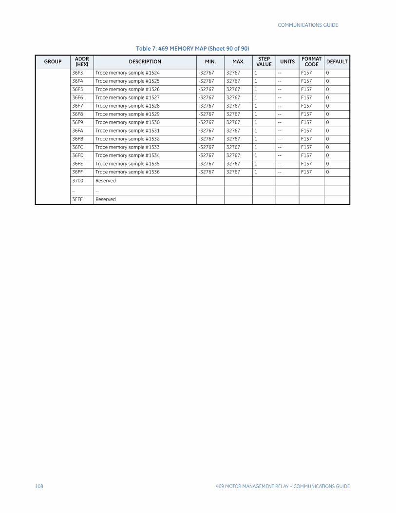
108 469 MOTOR MANAGEMENT RELAY – COMMUNICATIONS GUIDE
COMMUNICATIONS GUIDE
36F3 Trace memory sample #1524 -32767 32767 1 -- F157 0
36F4 Trace memory sample #1525 -32767 32767 1 -- F157 0
36F5 Trace memory sample #1526 -32767 32767 1 -- F157 0
36F6 Trace memory sample #1527 -32767 32767 1 -- F157 0
36F7 Trace memory sample #1528 -32767 32767 1 -- F157 0
36F8 Trace memory sample #1529 -32767 32767 1 -- F157 0
36F9 Trace memory sample #1530 -32767 32767 1 -- F157 0
36FA Trace memory sample #1531 -32767 32767 1 -- F157 0
36FB Trace memory sample #1532 -32767 32767 1 -- F157 0
36FC Trace memory sample #1533 -32767 32767 1 -- F157 0
36FD Trace memory sample #1534 -32767 32767 1 -- F157 0
36FE Trace memory sample #1535 -32767 32767 1 -- F157 0
36FF Trace memory sample #1536 -32767 32767 1 -- F157 0
3700 Reserved
... ...
3FFF Reserved
Table 7: 469 MEMORY MAP (Sheet 90 of 90)
GROUP ADDR(HEX) DESCRIPTION MIN. MAX. STEP
VALUE UNITS FORMATCODE DEFAULT
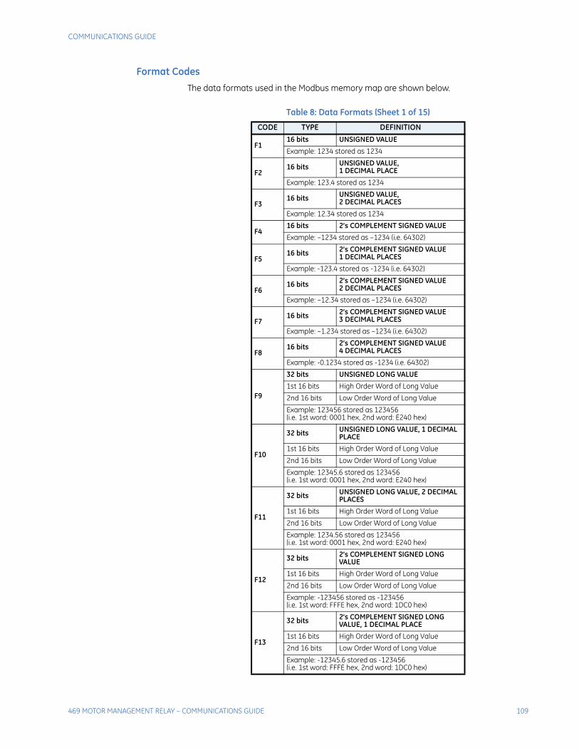
COMMUNICATIONS GUIDE
469 MOTOR MANAGEMENT RELAY – COMMUNICATIONS GUIDE 109
Format Codes
The data formats used in the Modbus memory map are shown below.
Table 8: Data Formats (Sheet 1 of 15)
CODE TYPE DEFINITION
F116 bits UNSIGNED VALUE
Example: 1234 stored as 1234
F216 bits UNSIGNED VALUE,
1 DECIMAL PLACE
Example: 123.4 stored as 1234
F316 bits UNSIGNED VALUE,
2 DECIMAL PLACES
Example: 12.34 stored as 1234
F416 bits 2’s COMPLEMENT SIGNED VALUE
Example: –1234 stored as –1234 (i.e. 64302)
F516 bits 2’s COMPLEMENT SIGNED VALUE
1 DECIMAL PLACES
Example: -123.4 stored as -1234 (i.e. 64302)
F616 bits 2’s COMPLEMENT SIGNED VALUE
2 DECIMAL PLACES
Example: –12.34 stored as –1234 (i.e. 64302)
F716 bits 2’s COMPLEMENT SIGNED VALUE
3 DECIMAL PLACES
Example: –1.234 stored as –1234 (i.e. 64302)
F816 bits 2’s COMPLEMENT SIGNED VALUE
4 DECIMAL PLACES
Example: -0.1234 stored as -1234 (i.e. 64302)
F9
32 bits UNSIGNED LONG VALUE
1st 16 bits High Order Word of Long Value
2nd 16 bits Low Order Word of Long Value
Example: 123456 stored as 123456(i.e. 1st word: 0001 hex, 2nd word: E240 hex)
F10
32 bits UNSIGNED LONG VALUE, 1 DECIMAL PLACE
1st 16 bits High Order Word of Long Value
2nd 16 bits Low Order Word of Long Value
Example: 12345.6 stored as 123456(i.e. 1st word: 0001 hex, 2nd word: E240 hex)
F11
32 bits UNSIGNED LONG VALUE, 2 DECIMAL PLACES
1st 16 bits High Order Word of Long Value
2nd 16 bits Low Order Word of Long Value
Example: 1234.56 stored as 123456(i.e. 1st word: 0001 hex, 2nd word: E240 hex)
F12
32 bits 2’s COMPLEMENT SIGNED LONG VALUE
1st 16 bits High Order Word of Long Value
2nd 16 bits Low Order Word of Long Value
Example: -123456 stored as -123456(i.e. 1st word: FFFE hex, 2nd word: 1DC0 hex)
F13
32 bits 2’s COMPLEMENT SIGNED LONG VALUE, 1 DECIMAL PLACE
1st 16 bits High Order Word of Long Value
2nd 16 bits Low Order Word of Long Value
Example: -12345.6 stored as -123456(i.e. 1st word: FFFE hex, 2nd word: 1DC0 hex)
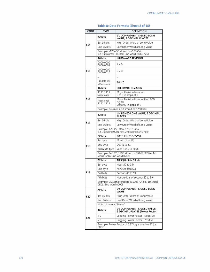
110 469 MOTOR MANAGEMENT RELAY – COMMUNICATIONS GUIDE
COMMUNICATIONS GUIDE
F14
32 bits 2’s COMPLEMENT SIGNED LONG VALUE, 2 DECIMAL PLACES
1st 16 bits High Order Word of Long Value
2nd 16 bits Low Order Word of Long Value
Example: -1234.56 stored as -123456(i.e. 1st word: FFFE hex, 2nd word: 1DC0 hex)
F15
16 bits HARDWARE REVISION
0000 0000 0000 0001 1 = A
0000 0000 0000 0010 2 = B
... ...
0000 0000 0001 1010 26 = Z
F16
16 bits SOFTWARE REVISION
1111 1111 xxxx xxxx
Major Revision Number0 to 9 in steps of 1
xxxx xxxx 1111 1111
Minor Revision Number (two BCD digits)00 to 99 in steps of 1
Example: Revision 2.30 stored as 0230 hex
F17
32 bits UNSIGNED LONG VALUE, 3 DECIMAL PLACES
1st 16 bits High Order Word of Long Value
2nd 16 bits Low Order Word of Long Value
Example: 123.456 stored as 123456(i.e. 1st word: 0001 hex, 2nd word: E240 hex)
F18
32 bits DATE (MM/DD/YYYY)
1st byte Month (1 to 12)
2nd byte Day (1 to 31)
3rd & 4th byte Year (1995 to 2094)
Example: Feb. 20, 1995 stored as 34867142 (i.e. 1st word: 0214, 2nd word 07C6)
F19
32 bits TIME (HH:MM:SS:hh)
1st byte Hours (0 to 23)
2nd byte Minutes (0 to 59)
3rd byte Seconds (0 to 59)
4th byte Hundredths of seconds (0 to 99)
Example: 2:05pm stored as 235208704 (i.e. 1st word: 0E05, 2nd word 0000)
F20
32 bits 2’s COMPLEMENT SIGNED LONG VALUE
1st 16 bits High Order Word of Long Value
2nd 16 bits Low Order Word of Long Value
Note: -1 means “Never”
F21
16 bits 2’s COMPLEMENT SIGNED VALUE2 DECIMAL PLACES (Power Factor)
< 0 Leading Power Factor - Negative
> 0 Lagging Power Factor - Positive
Example: Power Factor of 0.87 lag is used as 87 (i.e. 0057)
Table 8: Data Formats (Sheet 2 of 15)
CODE TYPE DEFINITION
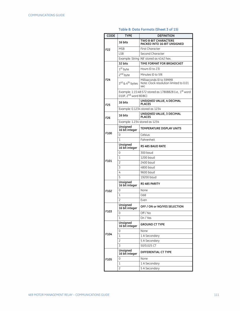
COMMUNICATIONS GUIDE
469 MOTOR MANAGEMENT RELAY – COMMUNICATIONS GUIDE 111
F22
16 bits TWO 8-BIT CHARACTERSPACKED INTO 16-BIT UNSIGNED
MSB First Character
LSB Second Character
Example: String ‘AB’ stored as 4142 hex.
F24
32 bits TIME FORMAT FOR BROADCAST
1st byte Hours (0 to 23)
2nd byte Minutes (0 to 59)
3rd & 4th bytesMilliseconds (0 to 59999)Note: Clock resolution limited to 0.01 sec
Example: 1:15:48:572 stored as 17808828 (i.e., 1st word 010F, 2nd word BDBC)
F2516 bits UNSIGNED VALUE, 4 DECIMAL
PLACES
Example: 0.1234 stored as 1234
F2616 bits UNSIGNED VALUE, 3 DECIMAL
PLACES
Example: 1.234 stored as 1234
F100
Unsigned16 bit integer TEMPERATURE DISPLAY UNITS
0 Celsius
1 Fahrenheit
F101
Unsigned16 bit integer RS 485 BAUD RATE
0 300 baud
1 1200 baud
2 2400 baud
3 4800 baud
4 9600 baud
5 19200 baud
F102
Unsigned16 bit integer RS 485 PARITY
0 None
1 Odd
2 Even
F103
Unsigned16 bit integer OFF / ON or NO/YES SELECTION
0 Off / No
1 On / Yes
F104
Unsigned16 bit integer GROUND CT TYPE
0 None
1 1 A Secondary
2 5 A Secondary
3 50/0.025 CT
F105
Unsigned16 bit integer DIFFERENTIAL CT TYPE
0 None
1 1 A Secondary
2 5 A Secondary
Table 8: Data Formats (Sheet 3 of 15)
CODE TYPE DEFINITION
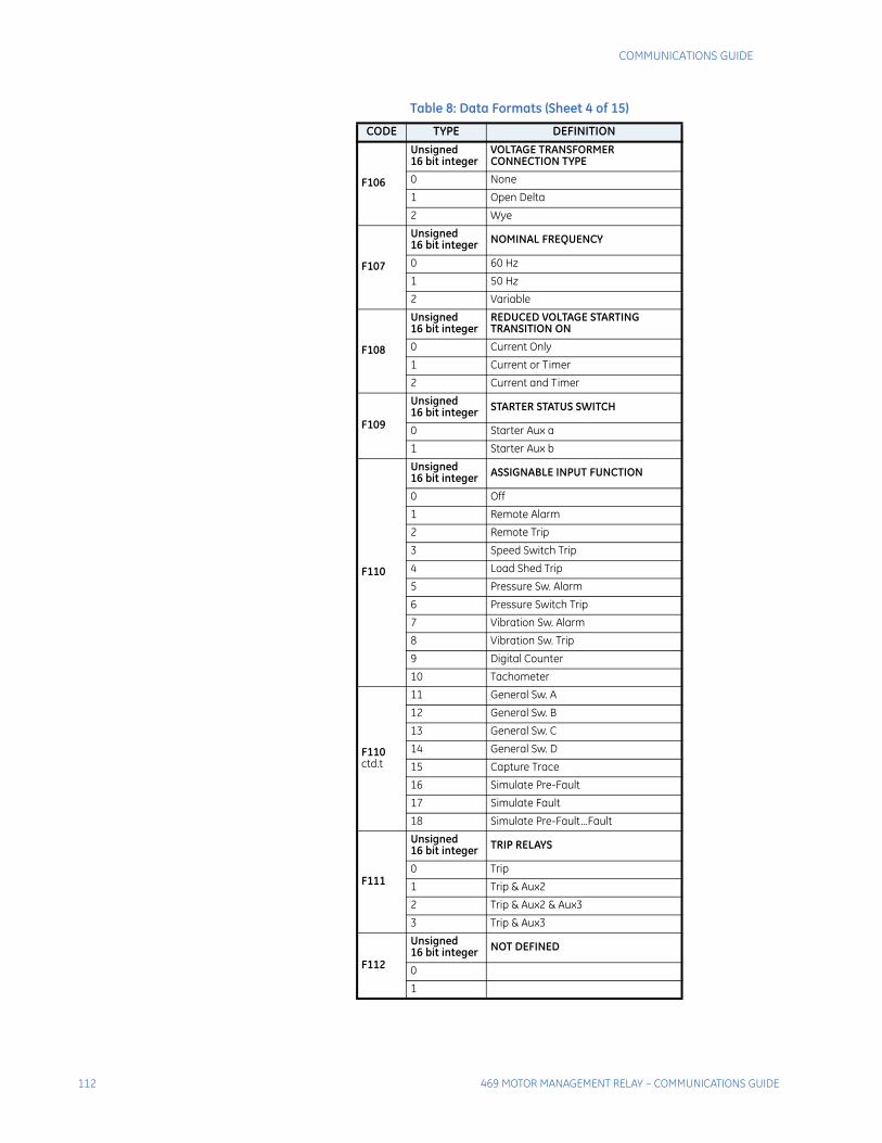
112 469 MOTOR MANAGEMENT RELAY – COMMUNICATIONS GUIDE
COMMUNICATIONS GUIDE
F106
Unsigned16 bit integer
VOLTAGE TRANSFORMER CONNECTION TYPE
0 None
1 Open Delta
2 Wye
F107
Unsigned16 bit integer NOMINAL FREQUENCY
0 60 Hz
1 50 Hz
2 Variable
F108
Unsigned16 bit integer
REDUCED VOLTAGE STARTING TRANSITION ON
0 Current Only
1 Current or Timer
2 Current and Timer
F109
Unsigned16 bit integer STARTER STATUS SWITCH
0 Starter Aux a
1 Starter Aux b
F110
Unsigned16 bit integer ASSIGNABLE INPUT FUNCTION
0 Off
1 Remote Alarm
2 Remote Trip
3 Speed Switch Trip
4 Load Shed Trip
5 Pressure Sw. Alarm
6 Pressure Switch Trip
7 Vibration Sw. Alarm
8 Vibration Sw. Trip
9 Digital Counter
10 Tachometer
F110ctd.t
11 General Sw. A
12 General Sw. B
13 General Sw. C
14 General Sw. D
15 Capture Trace
16 Simulate Pre-Fault
17 Simulate Fault
18 Simulate Pre-Fault ...Fault
F111
Unsigned16 bit integer TRIP RELAYS
0 Trip
1 Trip & Aux2
2 Trip & Aux2 & Aux3
3 Trip & Aux3
F112
Unsigned16 bit integer NOT DEFINED
0
1
Table 8: Data Formats (Sheet 4 of 15)
CODE TYPE DEFINITION
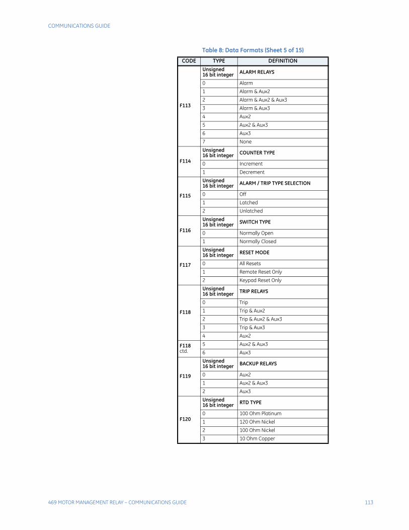
COMMUNICATIONS GUIDE
469 MOTOR MANAGEMENT RELAY – COMMUNICATIONS GUIDE 113
F113
Unsigned16 bit integer ALARM RELAYS
0 Alarm
1 Alarm & Aux2
2 Alarm & Aux2 & Aux3
3 Alarm & Aux3
4 Aux2
5 Aux2 & Aux3
6 Aux3
7 None
F114
Unsigned16 bit integer COUNTER TYPE
0 Increment
1 Decrement
F115
Unsigned16 bit integer ALARM / TRIP TYPE SELECTION
0 Off
1 Latched
2 Unlatched
F116
Unsigned16 bit integer SWITCH TYPE
0 Normally Open
1 Normally Closed
F117
Unsigned 16 bit integer RESET MODE
0 All Resets
1 Remote Reset Only
2 Keypad Reset Only
F118
Unsigned 16 bit integer TRIP RELAYS
0 Trip
1 Trip & Aux2
2 Trip & Aux2 & Aux3
3 Trip & Aux3
4 Aux2
F118ctd.
5 Aux2 & Aux3
6 Aux3
F119
Unsigned16 bit integer BACKUP RELAYS
0 Aux2
1 Aux2 & Aux3
2 Aux3
F120
Unsigned16 bit integer RTD TYPE
0 100 Ohm Platinum
1 120 Ohm Nickel
2 100 Ohm Nickel
3 10 Ohm Copper
Table 8: Data Formats (Sheet 5 of 15)
CODE TYPE DEFINITION
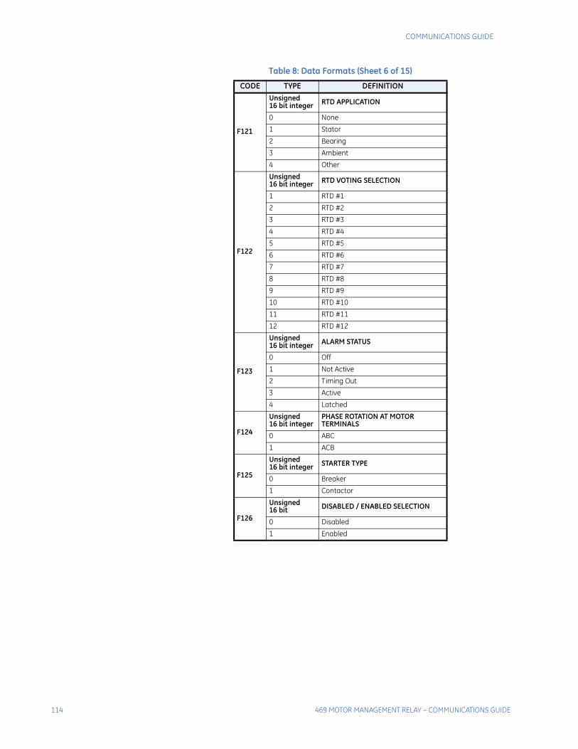
114 469 MOTOR MANAGEMENT RELAY – COMMUNICATIONS GUIDE
COMMUNICATIONS GUIDE
F121
Unsigned16 bit integer RTD APPLICATION
0 None
1 Stator
2 Bearing
3 Ambient
4 Other
F122
Unsigned16 bit integer RTD VOTING SELECTION
1 RTD #1
2 RTD #2
3 RTD #3
4 RTD #4
5 RTD #5
6 RTD #6
7 RTD #7
8 RTD #8
9 RTD #9
10 RTD #10
11 RTD #11
12 RTD #12
F123
Unsigned16 bit integer ALARM STATUS
0 Off
1 Not Active
2 Timing Out
3 Active
4 Latched
F124
Unsigned 16 bit integer
PHASE ROTATION AT MOTOR TERMINALS
0 ABC
1 ACB
F125
Unsigned 16 bit integer STARTER TYPE
0 Breaker
1 Contactor
F126
Unsigned16 bit DISABLED / ENABLED SELECTION
0 Disabled
1 Enabled
Table 8: Data Formats (Sheet 6 of 15)
CODE TYPE DEFINITION
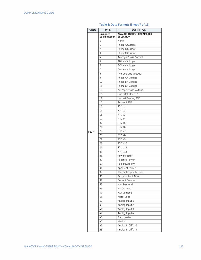
COMMUNICATIONS GUIDE
469 MOTOR MANAGEMENT RELAY – COMMUNICATIONS GUIDE 115
F127
Unsigned16 bit integer
ANALOG OUTPUT PARAMETER SELECTION
0 None
1 Phase A Current
2 Phase B Current
3 Phase C Current
4 Average Phase Current
5 AB Line Voltage
6 BC Line Voltage
7 CA Line Voltage
8 Average Line Voltage
9 Phase AN Voltage
10 Phase BN Voltage
11 Phase CN Voltage
12 Average Phase Voltage
13 Hottest Stator RTD
14 Hottest Bearing RTD
15 Ambient RTD
16 RTD #1
17 RTD #2
18 RTD #3
19 RTD #4
20 RTD #5
21 RTD #6
22 RTD #7
23 RTD #8
24 RTD #9
25 RTD #10
26 RTD #11
27 RTD #12
28 Power Factor
29 Reactive Power
30 Real Power (kW)
31 Apparent Power
32 Thermal Capacity Used
33 Relay Lockout Time
34 Current Demand
35 kvar Demand
36 kW Demand
37 kVA Demand
38 Motor Load
39 Analog Input 1
40 Analog Input 2
41 Analog Input 3
42 Analog Input 4
43 Tachometer
44 MWhrs
45 Analog In Diff 1-2
46 Analog In Diff 3-4
Table 8: Data Formats (Sheet 7 of 15)
CODE TYPE DEFINITION
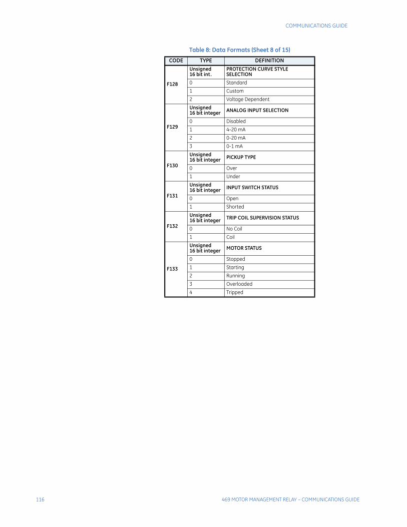
116 469 MOTOR MANAGEMENT RELAY – COMMUNICATIONS GUIDE
COMMUNICATIONS GUIDE
F128
Unsigned16 bit int.
PROTECTION CURVE STYLE SELECTION
0 Standard
1 Custom
2 Voltage Dependent
F129
Unsigned16 bit integer ANALOG INPUT SELECTION
0 Disabled
1 4-20 mA
2 0-20 mA
3 0-1 mA
F130
Unsigned16 bit integer PICKUP TYPE
0 Over
1 Under
F131
Unsigned16 bit integer INPUT SWITCH STATUS
0 Open
1 Shorted
F132
Unsigned16 bit integer TRIP COIL SUPERVISION STATUS
0 No Coil
1 Coil
F133
Unsigned16 bit integer MOTOR STATUS
0 Stopped
1 Starting
2 Running
3 Overloaded
4 Tripped
Table 8: Data Formats (Sheet 8 of 15)
CODE TYPE DEFINITION
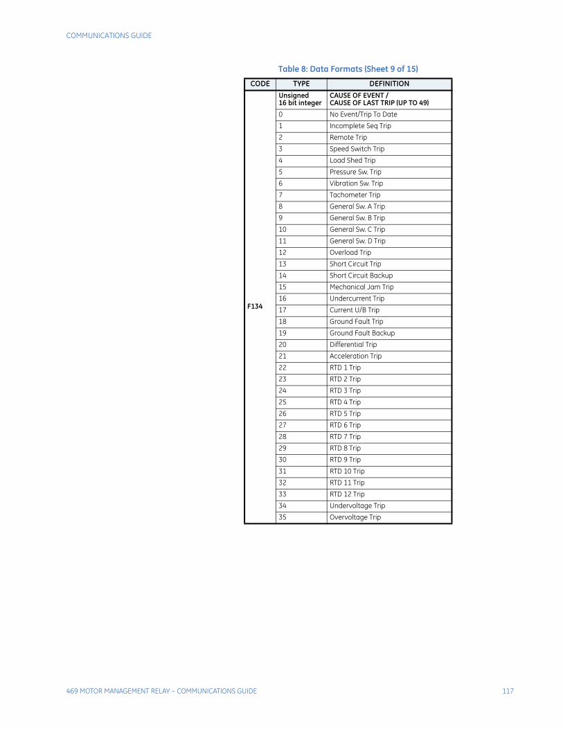
COMMUNICATIONS GUIDE
469 MOTOR MANAGEMENT RELAY – COMMUNICATIONS GUIDE 117
F134
Unsigned16 bit integer
CAUSE OF EVENT / CAUSE OF LAST TRIP (UP TO 49)
0 No Event/Trip To Date
1 Incomplete Seq Trip
2 Remote Trip
3 Speed Switch Trip
4 Load Shed Trip
5 Pressure Sw. Trip
6 Vibration Sw. Trip
7 Tachometer Trip
8 General Sw. A Trip
9 General Sw. B Trip
10 General Sw. C Trip
11 General Sw. D Trip
12 Overload Trip
13 Short Circuit Trip
14 Short Circuit Backup
15 Mechanical Jam Trip
16 Undercurrent Trip
17 Current U/B Trip
18 Ground Fault Trip
19 Ground Fault Backup
20 Differential Trip
21 Acceleration Trip
22 RTD 1 Trip
23 RTD 2 Trip
24 RTD 3 Trip
25 RTD 4 Trip
26 RTD 5 Trip
27 RTD 6 Trip
28 RTD 7 Trip
29 RTD 8 Trip
30 RTD 9 Trip
31 RTD 10 Trip
32 RTD 11 Trip
33 RTD 12 Trip
34 Undervoltage Trip
35 Overvoltage Trip
Table 8: Data Formats (Sheet 9 of 15)
CODE TYPE DEFINITION
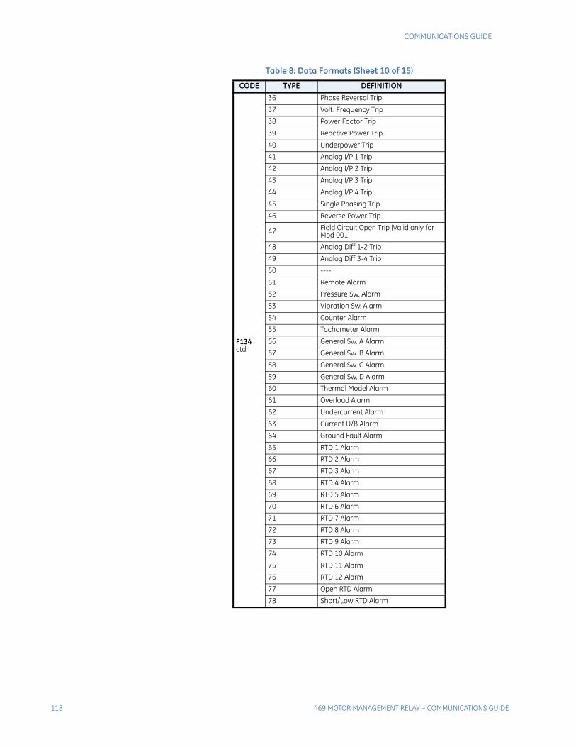
118 469 MOTOR MANAGEMENT RELAY – COMMUNICATIONS GUIDE
COMMUNICATIONS GUIDE
F134ctd.
36 Phase Reversal Trip
37 Volt. Frequency Trip
38 Power Factor Trip
39 Reactive Power Trip
40 Underpower Trip
41 Analog I/P 1 Trip
42 Analog I/P 2 Trip
43 Analog I/P 3 Trip
44 Analog I/P 4 Trip
45 Single Phasing Trip
46 Reverse Power Trip
47 Field Circuit Open Trip (Valid only for Mod 001)
48 Analog Diff 1-2 Trip
49 Analog Diff 3-4 Trip
50 ----
51 Remote Alarm
52 Pressure Sw. Alarm
53 Vibration Sw. Alarm
54 Counter Alarm
55 Tachometer Alarm
56 General Sw. A Alarm
57 General Sw. B Alarm
58 General Sw. C Alarm
59 General Sw. D Alarm
60 Thermal Model Alarm
61 Overload Alarm
62 Undercurrent Alarm
63 Current U/B Alarm
64 Ground Fault Alarm
65 RTD 1 Alarm
66 RTD 2 Alarm
67 RTD 3 Alarm
68 RTD 4 Alarm
69 RTD 5 Alarm
70 RTD 6 Alarm
71 RTD 7 Alarm
72 RTD 8 Alarm
73 RTD 9 Alarm
74 RTD 10 Alarm
75 RTD 11 Alarm
76 RTD 12 Alarm
77 Open RTD Alarm
78 Short/Low RTD Alarm
Table 8: Data Formats (Sheet 10 of 15)
CODE TYPE DEFINITION
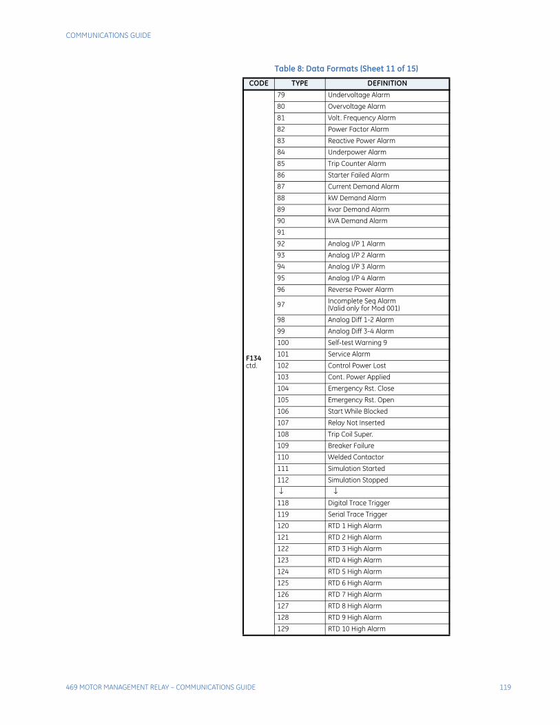
COMMUNICATIONS GUIDE
469 MOTOR MANAGEMENT RELAY – COMMUNICATIONS GUIDE 119
F134ctd.
79 Undervoltage Alarm
80 Overvoltage Alarm
81 Volt. Frequency Alarm
82 Power Factor Alarm
83 Reactive Power Alarm
84 Underpower Alarm
85 Trip Counter Alarm
86 Starter Failed Alarm
87 Current Demand Alarm
88 kW Demand Alarm
89 kvar Demand Alarm
90 kVA Demand Alarm
91
92 Analog I/P 1 Alarm
93 Analog I/P 2 Alarm
94 Analog I/P 3 Alarm
95 Analog I/P 4 Alarm
96 Reverse Power Alarm
97 Incomplete Seq Alarm(Valid only for Mod 001)
98 Analog Diff 1-2 Alarm
99 Analog Diff 3-4 Alarm
100 Self-test Warning 9
101 Service Alarm
102 Control Power Lost
103 Cont. Power Applied
104 Emergency Rst. Close
105 Emergency Rst. Open
106 Start While Blocked
107 Relay Not Inserted
108 Trip Coil Super.
109 Breaker Failure
110 Welded Contactor
111 Simulation Started
112 Simulation Stopped
↓ ↓118 Digital Trace Trigger
119 Serial Trace Trigger
120 RTD 1 High Alarm
121 RTD 2 High Alarm
122 RTD 3 High Alarm
123 RTD 4 High Alarm
124 RTD 5 High Alarm
125 RTD 6 High Alarm
126 RTD 7 High Alarm
127 RTD 8 High Alarm
128 RTD 9 High Alarm
129 RTD 10 High Alarm
Table 8: Data Formats (Sheet 11 of 15)
CODE TYPE DEFINITION
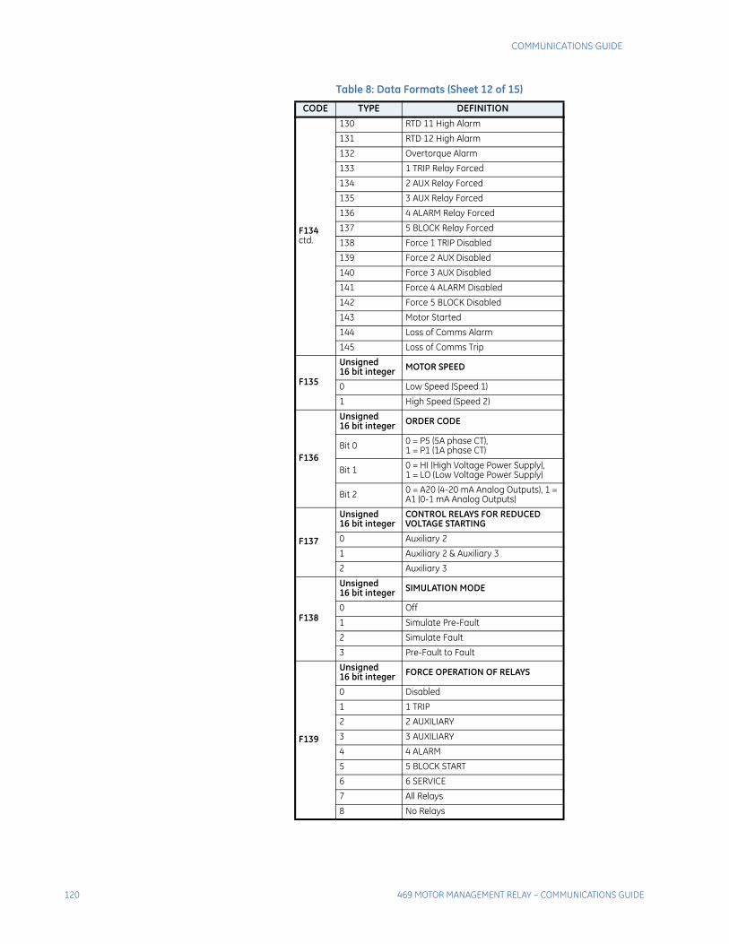
120 469 MOTOR MANAGEMENT RELAY – COMMUNICATIONS GUIDE
COMMUNICATIONS GUIDE
F134ctd.
130 RTD 11 High Alarm
131 RTD 12 High Alarm
132 Overtorque Alarm
133 1 TRIP Relay Forced
134 2 AUX Relay Forced
135 3 AUX Relay Forced
136 4 ALARM Relay Forced
137 5 BLOCK Relay Forced
138 Force 1 TRIP Disabled
139 Force 2 AUX Disabled
140 Force 3 AUX Disabled
141 Force 4 ALARM Disabled
142 Force 5 BLOCK Disabled
143 Motor Started
144 Loss of Comms Alarm
145 Loss of Comms Trip
F135
Unsigned16 bit integer MOTOR SPEED
0 Low Speed (Speed 1)
1 High Speed (Speed 2)
F136
Unsigned16 bit integer ORDER CODE
Bit 0 0 = P5 (5A phase CT),1 = P1 (1A phase CT)
Bit 1 0 = HI (High Voltage Power Supply),1 = LO (Low Voltage Power Supply)
Bit 2 0 = A20 (4-20 mA Analog Outputs), 1 = A1 (0-1 mA Analog Outputs)
F137
Unsigned16 bit integer
CONTROL RELAYS FOR REDUCED VOLTAGE STARTING
0 Auxiliary 2
1 Auxiliary 2 & Auxiliary 3
2 Auxiliary 3
F138
Unsigned16 bit integer SIMULATION MODE
0 Off
1 Simulate Pre-Fault
2 Simulate Fault
3 Pre-Fault to Fault
F139
Unsigned 16 bit integer FORCE OPERATION OF RELAYS
0 Disabled
1 1 TRIP
2 2 AUXILIARY
3 3 AUXILIARY
4 4 ALARM
5 5 BLOCK START
6 6 SERVICE
7 All Relays
8 No Relays
Table 8: Data Formats (Sheet 12 of 15)
CODE TYPE DEFINITION
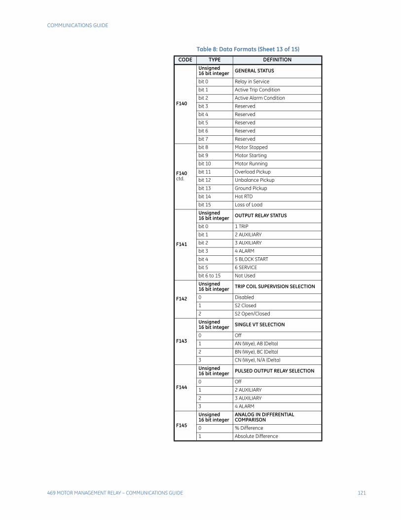
COMMUNICATIONS GUIDE
469 MOTOR MANAGEMENT RELAY – COMMUNICATIONS GUIDE 121
F140
Unsigned 16 bit integer GENERAL STATUS
bit 0 Relay in Service
bit 1 Active Trip Condition
bit 2 Active Alarm Condition
bit 3 Reserved
bit 4 Reserved
bit 5 Reserved
bit 6 Reserved
bit 7 Reserved
F140ctd.
bit 8 Motor Stopped
bit 9 Motor Starting
bit 10 Motor Running
bit 11 Overload Pickup
bit 12 Unbalance Pickup
bit 13 Ground Pickup
bit 14 Hot RTD
bit 15 Loss of Load
F141
Unsigned16 bit integer OUTPUT RELAY STATUS
bit 0 1 TRIP
bit 1 2 AUXILIARY
bit 2 3 AUXILIARY
bit 3 4 ALARM
bit 4 5 BLOCK START
bit 5 6 SERVICE
bit 6 to 15 Not Used
F142
Unsigned16 bit integer TRIP COIL SUPERVISION SELECTION
0 Disabled
1 S2 Closed
2 S2 Open/Closed
F143
Unsigned16 bit integer SINGLE VT SELECTION
0 Off
1 AN (Wye), AB (Delta)
2 BN (Wye), BC (Delta)
3 CN (Wye), N/A (Delta)
F144
Unsigned 16 bit integer PULSED OUTPUT RELAY SELECTION
0 Off
1 2 AUXILIARY
2 3 AUXILIARY
3 4 ALARM
F145
Unsigned16 bit integer
ANALOG IN DIFFERENTIAL COMPARISON
0 % Difference
1 Absolute Difference
Table 8: Data Formats (Sheet 13 of 15)
CODE TYPE DEFINITION
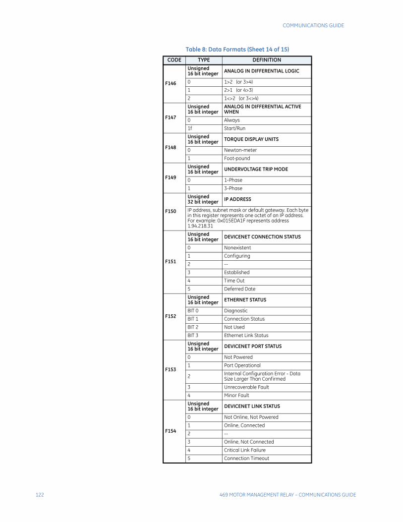
122 469 MOTOR MANAGEMENT RELAY – COMMUNICATIONS GUIDE
COMMUNICATIONS GUIDE
F146
Unsigned16 bit integer ANALOG IN DIFFERENTIAL LOGIC
0 1>2 (or 3>4)
1 2>1 (or 4>3)
2 1<>2 (or 3<>4)
F147
Unsigned16 bit integer
ANALOG IN DIFFERENTIAL ACTIVE WHEN
0 Always
1f Start/Run
F148
Unsigned16 bit integer TORQUE DISPLAY UNITS
0 Newton-meter
1 Foot-pound
F149
Unsigned16 bit integer UNDERVOLTAGE TRIP MODE
0 1-Phase
1 3-Phase
F150
Unsigned32 bit integer IP ADDRESS
IP address, subnet mask or default gateway. Each byte in this register represents one octet of an IP address. For example: 0x015EDA1F represents address 1.94.218.31
F151
Unsigned16 bit integer DEVICENET CONNECTION STATUS
0 Nonexistent
1 Configuring
2 --
3 Established
4 Time Out
5 Deferred Date
F152
Unsigned16 bit integer ETHERNET STATUS
BIT 0 Diagnostic
BIT 1 Connection Status
BIT 2 Not Used
BIT 3 Ethernet Link Status
F153
Unsigned16 bit integer DEVICENET PORT STATUS
0 Not Powered
1 Port Operational
2 Internal Configuration Error - Data Size Larger Than Confirmed
3 Unrecoverable Fault
4 Minor Fault
F154
Unsigned16 bit integer DEVICENET LINK STATUS
0 Not Online, Not Powered
1 Online, Connected
2 --
3 Online, Not Connected
4 Critical Link Failure
5 Connection Timeout
Table 8: Data Formats (Sheet 14 of 15)
CODE TYPE DEFINITION
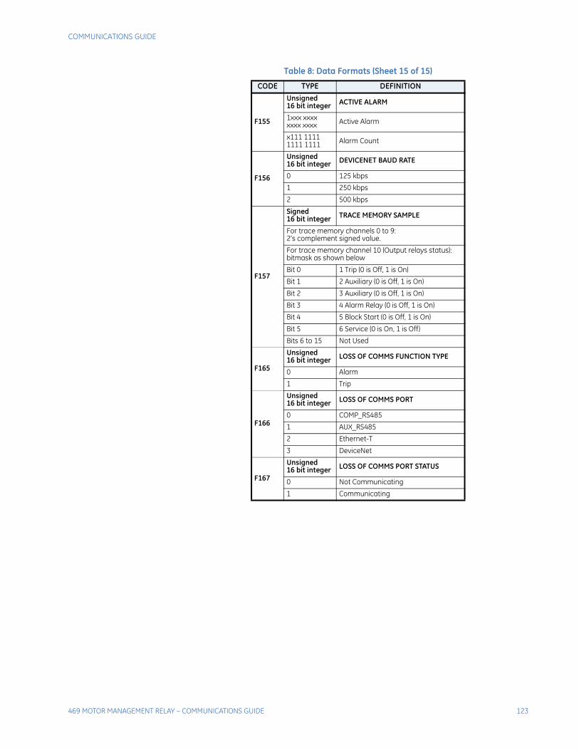
COMMUNICATIONS GUIDE
469 MOTOR MANAGEMENT RELAY – COMMUNICATIONS GUIDE 123
F155
Unsigned16 bit integer ACTIVE ALARM
1xxx xxxx xxxx xxxx Active Alarm
x111 1111 1111 1111 Alarm Count
F156
Unsigned16 bit integer DEVICENET BAUD RATE
0 125 kbps
1 250 kbps
2 500 kbps
F157
Signed16 bit integer TRACE MEMORY SAMPLE
For trace memory channels 0 to 9: 2’s complement signed value.
For trace memory channel 10 (Output relays status): bitmask as shown below
Bit 0 1 Trip (0 is Off, 1 is On)
Bit 1 2 Auxiliary (0 is Off, 1 is On)
Bit 2 3 Auxiliary (0 is Off, 1 is On)
Bit 3 4 Alarm Relay (0 is Off, 1 is On)
Bit 4 5 Block Start (0 is Off, 1 is On)
Bit 5 6 Service (0 is On, 1 is Off)
Bits 6 to 15 Not Used
F165
Unsigned16 bit integer LOSS OF COMMS FUNCTION TYPE
0 Alarm
1 Trip
F166
Unsigned16 bit integer LOSS OF COMMS PORT
0 COMP_RS485
1 AUX_RS485
2 Ethernet-T
3 DeviceNet
F167
Unsigned16 bit integer LOSS OF COMMS PORT STATUS
0 Not Communicating
1 Communicating
Table 8: Data Formats (Sheet 15 of 15)
CODE TYPE DEFINITION
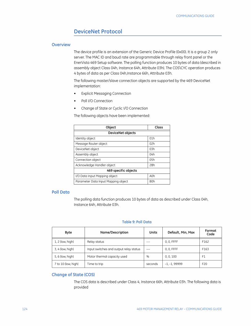
124 469 MOTOR MANAGEMENT RELAY – COMMUNICATIONS GUIDE
COMMUNICATIONS GUIDE
DeviceNet Protocol
Overview
The device profile is an extension of the Generic Device Profile (0x00). It is a group 2 only server. The MAC ID and baud rate are programmable through relay front panel or the EnerVista 469 Setup software. The polling function produces 10 bytes of data (described in assembly object Class 04h, Instance 64h, Attribute 03h). The COS\CYC operation produces 4 bytes of data as per Class 04h,Instance 66h, Attribute 03h.
The following master/slave connection objects are supported by the 469 DeviceNet implementation:
• Explicit Messaging Connection
• Poll I/O Connection
• Change of State or Cyclic I/O Connection
The following objects have been implemented:
Poll Data
The polling data function produces 10 bytes of data as described under Class 04h, Instance 64h, Attribute 03h.
Change of State (COS)
The COS data is described under Class 4, Instance 66h, Attribute 03h. The following data is provided
Object Class
DeviceNet objects
Identity object 01h
Message Router object 02h
DeviceNet object 03h
Assembly object 04h
Connection object 05h
Acknowledge Handler object 2Bh
469 specific objects
I/O Data Input Mapping object A0h
Parameter Data Input Mapping object B0h
Table 9: Poll Data
Byte Name/Description Units Default, Min, Max Format Code
1, 2 (low, high) Relay status --- 0, 0, FFFF F162
3, 4 (low, high) Input switches and output relay status --- 0, 0, FFFF F163
5, 6 (low, high) Motor thermal capacity used % 0, 0, 100 F1
7 to 10 (low, high) Time to trip seconds -1, -1, 99999 F20
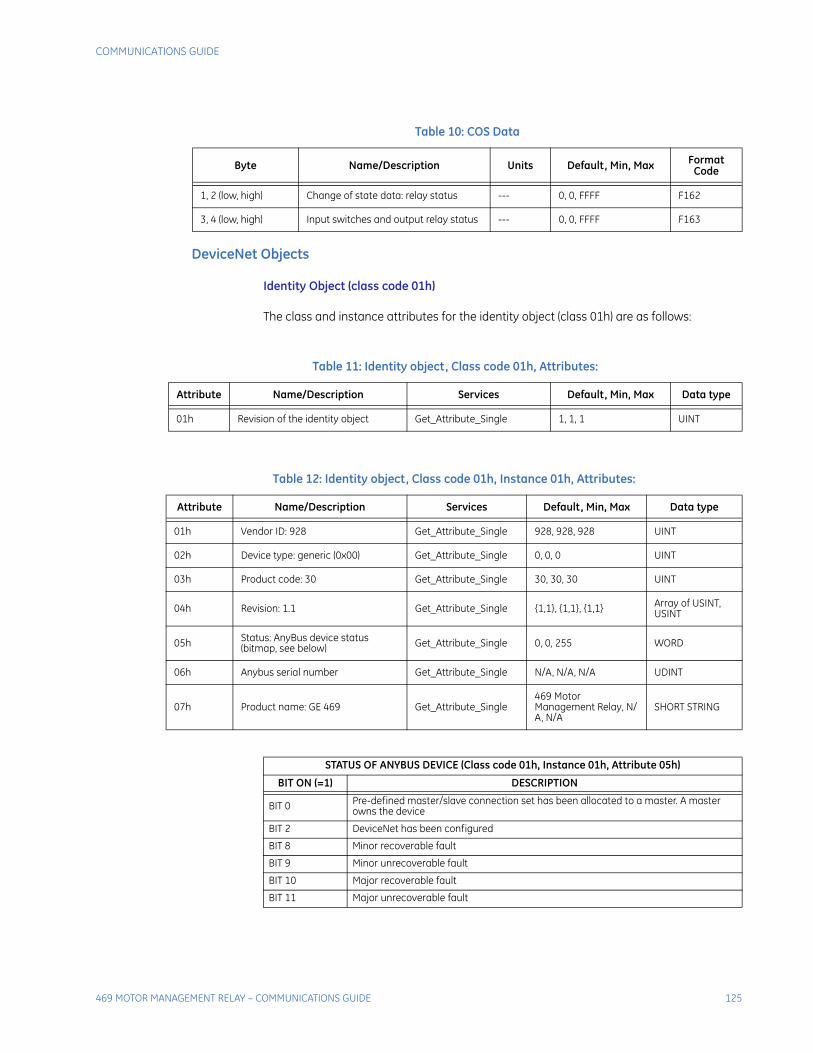
COMMUNICATIONS GUIDE
469 MOTOR MANAGEMENT RELAY – COMMUNICATIONS GUIDE 125
DeviceNet Objects
Identity Object (class code 01h)
The class and instance attributes for the identity object (class 01h) are as follows:
Table 10: COS Data
Byte Name/Description Units Default, Min, Max Format Code
1, 2 (low, high) Change of state data: relay status --- 0, 0, FFFF F162
3, 4 (low, high) Input switches and output relay status --- 0, 0, FFFF F163
Table 11: Identity object, Class code 01h, Attributes:
Attribute Name/Description Services Default, Min, Max Data type
01h Revision of the identity object Get_Attribute_Single 1, 1, 1 UINT
Table 12: Identity object, Class code 01h, Instance 01h, Attributes:
Attribute Name/Description Services Default, Min, Max Data type
01h Vendor ID: 928 Get_Attribute_Single 928, 928, 928 UINT
02h Device type: generic (0x00) Get_Attribute_Single 0, 0, 0 UINT
03h Product code: 30 Get_Attribute_Single 30, 30, 30 UINT
04h Revision: 1.1 Get_Attribute_Single {1,1}, {1,1}, {1,1} Array of USINT, USINT
05h Status: AnyBus device status (bitmap, see below) Get_Attribute_Single 0, 0, 255 WORD
06h Anybus serial number Get_Attribute_Single N/A, N/A, N/A UDINT
07h Product name: GE 469 Get_Attribute_Single469 Motor Management Relay, N/A, N/A
SHORT STRING
STATUS OF ANYBUS DEVICE (Class code 01h, Instance 01h, Attribute 05h)
BIT ON (=1) DESCRIPTION
BIT 0 Pre-defined master/slave connection set has been allocated to a master. A master owns the device
BIT 2 DeviceNet has been configured
BIT 8 Minor recoverable fault
BIT 9 Minor unrecoverable fault
BIT 10 Major recoverable fault
BIT 11 Major unrecoverable fault
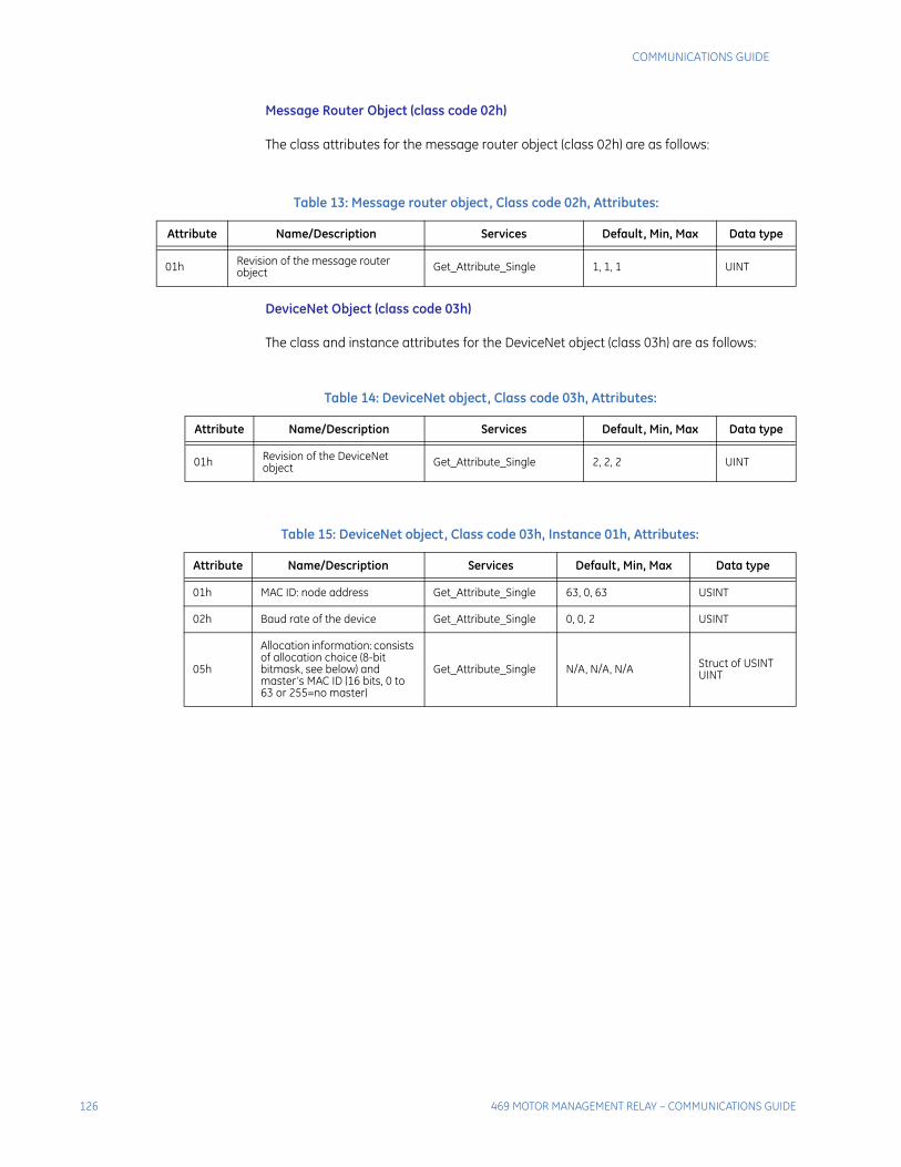
126 469 MOTOR MANAGEMENT RELAY – COMMUNICATIONS GUIDE
COMMUNICATIONS GUIDE
Message Router Object (class code 02h)
The class attributes for the message router object (class 02h) are as follows:
DeviceNet Object (class code 03h)
The class and instance attributes for the DeviceNet object (class 03h) are as follows:
Table 13: Message router object, Class code 02h, Attributes:
Attribute Name/Description Services Default, Min, Max Data type
01h Revision of the message router object Get_Attribute_Single 1, 1, 1 UINT
Table 14: DeviceNet object, Class code 03h, Attributes:
Attribute Name/Description Services Default, Min, Max Data type
01h Revision of the DeviceNet object Get_Attribute_Single 2, 2, 2 UINT
Table 15: DeviceNet object, Class code 03h, Instance 01h, Attributes:
Attribute Name/Description Services Default, Min, Max Data type
01h MAC ID: node address Get_Attribute_Single 63, 0, 63 USINT
02h Baud rate of the device Get_Attribute_Single 0, 0, 2 USINT
05h
Allocation information: consists of allocation choice (8-bit bitmask, see below) and master’s MAC ID (16 bits, 0 to 63 or 255=no master)
Get_Attribute_Single N/A, N/A, N/A Struct of USINT UINT
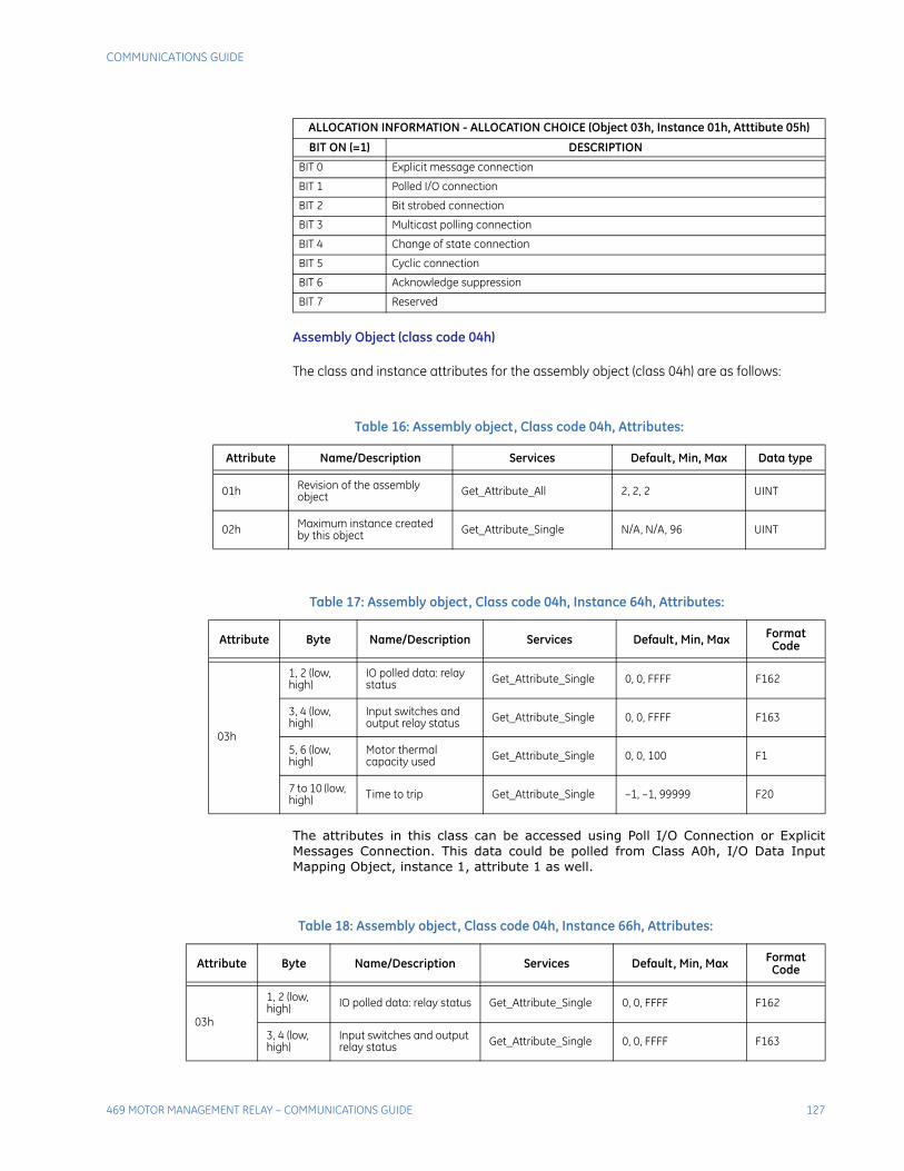
COMMUNICATIONS GUIDE
469 MOTOR MANAGEMENT RELAY – COMMUNICATIONS GUIDE 127
Assembly Object (class code 04h)
The class and instance attributes for the assembly object (class 04h) are as follows:
The attributes in this class can be accessed using Poll I/O Connection or ExplicitMessages Connection. This data could be polled from Class A0h, I/O Data InputMapping Object, instance 1, attribute 1 as well.
ALLOCATION INFORMATION - ALLOCATION CHOICE (Object 03h, Instance 01h, Atttibute 05h)
BIT ON (=1) DESCRIPTION
BIT 0 Explicit message connection
BIT 1 Polled I/O connection
BIT 2 Bit strobed connection
BIT 3 Multicast polling connection
BIT 4 Change of state connection
BIT 5 Cyclic connection
BIT 6 Acknowledge suppression
BIT 7 Reserved
Table 16: Assembly object, Class code 04h, Attributes:
Attribute Name/Description Services Default, Min, Max Data type
01h Revision of the assembly object Get_Attribute_All 2, 2, 2 UINT
02h Maximum instance created by this object Get_Attribute_Single N/A, N/A, 96 UINT
Table 17: Assembly object, Class code 04h, Instance 64h, Attributes:
Attribute Byte Name/Description Services Default, Min, Max Format Code
03h
1, 2 (low, high)
IO polled data: relay status Get_Attribute_Single 0, 0, FFFF F162
3, 4 (low, high)
Input switches and output relay status Get_Attribute_Single 0, 0, FFFF F163
5, 6 (low, high)
Motor thermal capacity used Get_Attribute_Single 0, 0, 100 F1
7 to 10 (low, high) Time to trip Get_Attribute_Single –1, –1, 99999 F20
Table 18: Assembly object, Class code 04h, Instance 66h, Attributes:
Attribute Byte Name/Description Services Default, Min, Max Format Code
03h
1, 2 (low, high) IO polled data: relay status Get_Attribute_Single 0, 0, FFFF F162
3, 4 (low, high)
Input switches and output relay status Get_Attribute_Single 0, 0, FFFF F163
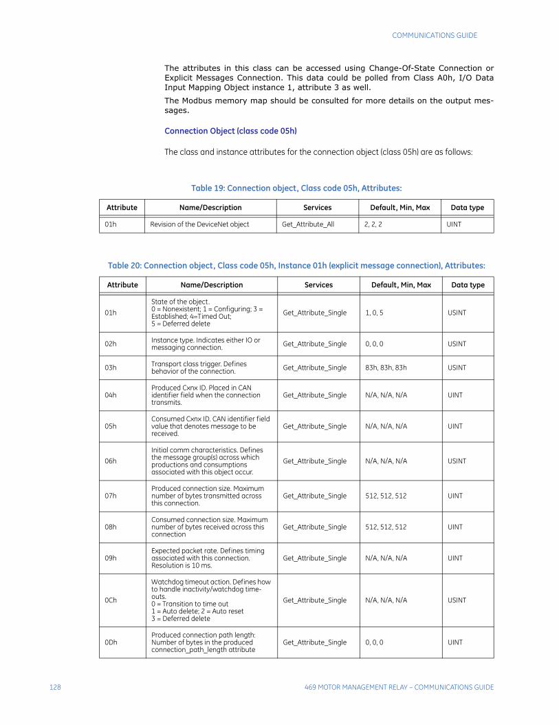
128 469 MOTOR MANAGEMENT RELAY – COMMUNICATIONS GUIDE
COMMUNICATIONS GUIDE
The attributes in this class can be accessed using Change-Of-State Connection orExplicit Messages Connection. This data could be polled from Class A0h, I/O DataInput Mapping Object instance 1, attribute 3 as well.
The Modbus memory map should be consulted for more details on the output mes-sages.
Connection Object (class code 05h)
The class and instance attributes for the connection object (class 05h) are as follows:
Table 19: Connection object, Class code 05h, Attributes:
Attribute Name/Description Services Default, Min, Max Data type
01h Revision of the DeviceNet object Get_Attribute_All 2, 2, 2 UINT
Table 20: Connection object, Class code 05h, Instance 01h (explicit message connection), Attributes:
Attribute Name/Description Services Default, Min, Max Data type
01h
State of the object.0 = Nonexistent; 1 = Configuring; 3 = Established; 4=Timed Out;5 = Deferred delete
Get_Attribute_Single 1, 0, 5 USINT
02h Instance type. Indicates either IO or messaging connection. Get_Attribute_Single 0, 0, 0 USINT
03h Transport class trigger. Defines behavior of the connection. Get_Attribute_Single 83h, 83h, 83h USINT
04hProduced Cxnx ID. Placed in CAN identifier field when the connection transmits.
Get_Attribute_Single N/A, N/A, N/A UINT
05hConsumed Cxnx ID. CAN identifier field value that denotes message to be received.
Get_Attribute_Single N/A, N/A, N/A UINT
06h
Initial comm characteristics. Defines the message group(s) across which productions and consumptions associated with this object occur.
Get_Attribute_Single N/A, N/A, N/A USINT
07hProduced connection size. Maximum number of bytes transmitted across this connection.
Get_Attribute_Single 512, 512, 512 UINT
08hConsumed connection size. Maximum number of bytes received across this connection
Get_Attribute_Single 512, 512, 512 UINT
09hExpected packet rate. Defines timing associated with this connection. Resolution is 10 ms.
Get_Attribute_Single N/A, N/A, N/A UINT
0Ch
Watchdog timeout action. Defines how to handle inactivity/watchdog time-outs.0 = Transition to time out1 = Auto delete; 2 = Auto reset3 = Deferred delete
Get_Attribute_Single N/A, N/A, N/A USINT
0DhProduced connection path length: Number of bytes in the produced connection_path_length attribute
Get_Attribute_Single 0, 0, 0 UINT
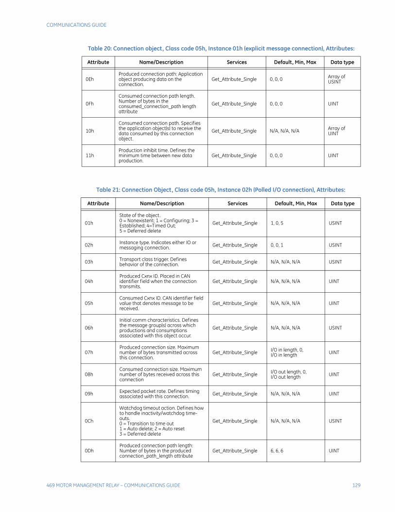
COMMUNICATIONS GUIDE
469 MOTOR MANAGEMENT RELAY – COMMUNICATIONS GUIDE 129
0EhProduced connection path: Application object producing data on the connection.
Get_Attribute_Single 0, 0, 0 Array of USINT
0Fh
Consumed connection path length. Number of bytes in the consumed_connection_path length attribute
Get_Attribute_Single 0, 0, 0 UINT
10h
Consumed connection path. Specifies the application object(s) to receive the data consumed by this connection object.
Get_Attribute_Single N/A, N/A, N/A Array of UINT
11hProduction inhibit time. Defines the minimum time between new data production.
Get_Attribute_Single 0, 0, 0 UINT
Table 20: Connection object, Class code 05h, Instance 01h (explicit message connection), Attributes:
Attribute Name/Description Services Default, Min, Max Data type
Table 21: Connection Object, Class code 05h, Instance 02h (Polled I/O connection), Attributes:
Attribute Name/Description Services Default, Min, Max Data type
01h
State of the object.0 = Nonexistent; 1 = Configuring; 3 = Established; 4=Timed Out;5 = Deferred delete
Get_Attribute_Single 1, 0, 5 USINT
02h Instance type. Indicates either IO or messaging connection. Get_Attribute_Single 0, 0, 1 USINT
03h Transport class trigger. Defines behavior of the connection. Get_Attribute_Single N/A, N/A, N/A USINT
04hProduced Cxnx ID. Placed in CAN identifier field when the connection transmits.
Get_Attribute_Single N/A, N/A, N/A UINT
05hConsumed Cxnx ID. CAN identifier field value that denotes message to be received.
Get_Attribute_Single N/A, N/A, N/A UINT
06h
Initial comm characteristics. Defines the message group(s) across which productions and consumptions associated with this object occur.
Get_Attribute_Single N/A, N/A, N/A USINT
07hProduced connection size. Maximum number of bytes transmitted across this connection.
Get_Attribute_Single I/O in length, 0,I/O in length UINT
08hConsumed connection size. Maximum number of bytes received across this connection
Get_Attribute_Single I/O out length, 0,I/O out length UINT
09h Expected packet rate. Defines timing associated with this connection. Get_Attribute_Single N/A, N/A, N/A UINT
0Ch
Watchdog timeout action. Defines how to handle inactivity/watchdog time-outs.0 = Transition to time out1 = Auto delete; 2 = Auto reset3 = Deferred delete
Get_Attribute_Single N/A, N/A, N/A USINT
0DhProduced connection path length: Number of bytes in the produced connection_path_length attribute
Get_Attribute_Single 6, 6, 6 UINT
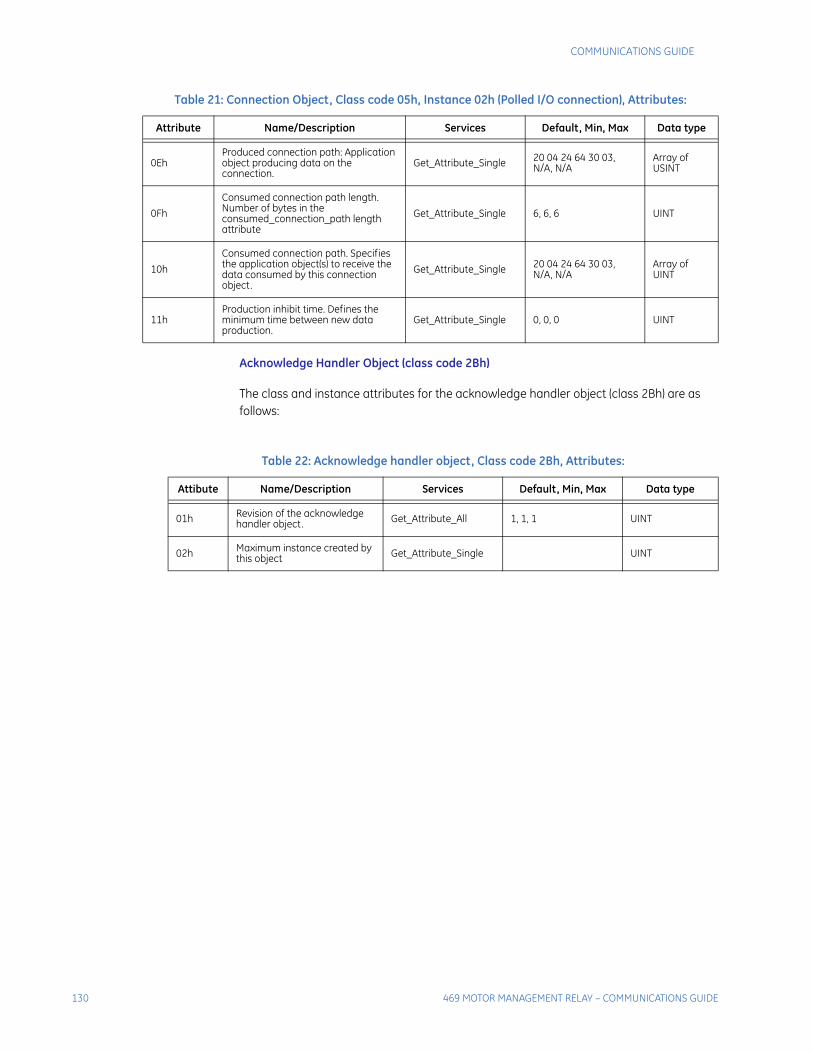
130 469 MOTOR MANAGEMENT RELAY – COMMUNICATIONS GUIDE
COMMUNICATIONS GUIDE
Acknowledge Handler Object (class code 2Bh)
The class and instance attributes for the acknowledge handler object (class 2Bh) are as follows:
0EhProduced connection path: Application object producing data on the connection.
Get_Attribute_Single 20 04 24 64 30 03, N/A, N/A
Array of USINT
0Fh
Consumed connection path length. Number of bytes in the consumed_connection_path length attribute
Get_Attribute_Single 6, 6, 6 UINT
10h
Consumed connection path. Specifies the application object(s) to receive the data consumed by this connection object.
Get_Attribute_Single 20 04 24 64 30 03, N/A, N/A
Array of UINT
11hProduction inhibit time. Defines the minimum time between new data production.
Get_Attribute_Single 0, 0, 0 UINT
Table 21: Connection Object, Class code 05h, Instance 02h (Polled I/O connection), Attributes:
Attribute Name/Description Services Default, Min, Max Data type
Table 22: Acknowledge handler object, Class code 2Bh, Attributes:
Attibute Name/Description Services Default, Min, Max Data type
01h Revision of the acknowledge handler object. Get_Attribute_All 1, 1, 1 UINT
02h Maximum instance created by this object Get_Attribute_Single UINT
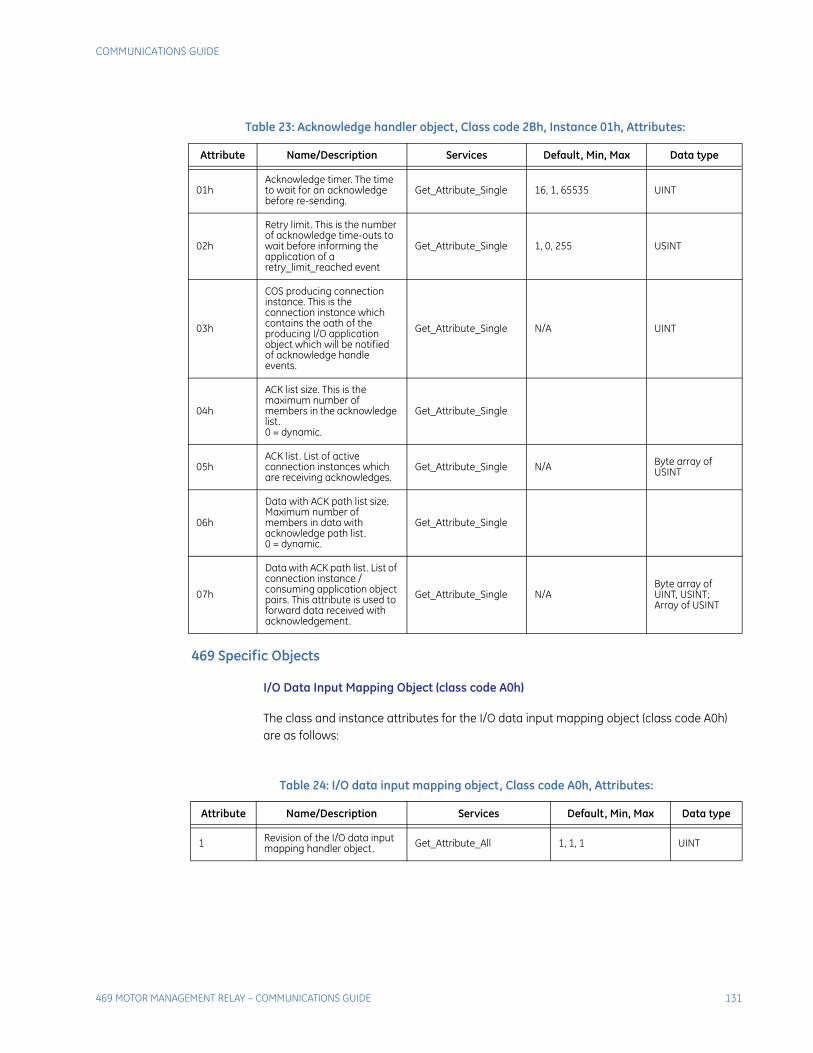
COMMUNICATIONS GUIDE
469 MOTOR MANAGEMENT RELAY – COMMUNICATIONS GUIDE 131
469 Specific Objects
I/O Data Input Mapping Object (class code A0h)
The class and instance attributes for the I/O data input mapping object (class code A0h) are as follows:
Table 23: Acknowledge handler object, Class code 2Bh, Instance 01h, Attributes:
Attribute Name/Description Services Default, Min, Max Data type
01hAcknowledge timer. The time to wait for an acknowledge before re-sending.
Get_Attribute_Single 16, 1, 65535 UINT
02h
Retry limit. This is the number of acknowledge time-outs to wait before informing the application of a retry_limit_reached event
Get_Attribute_Single 1, 0, 255 USINT
03h
COS producing connection instance. This is the connection instance which contains the oath of the producing I/O application object which will be notified of acknowledge handle events.
Get_Attribute_Single N/A UINT
04h
ACK list size. This is the maximum number of members in the acknowledge list.0 = dynamic.
Get_Attribute_Single
05hACK list . List of active connection instances which are receiving acknowledges.
Get_Attribute_Single N/A Byte array of USINT
06h
Data with ACK path list size. Maximum number of members in data with acknowledge path list.0 = dynamic.
Get_Attribute_Single
07h
Data with ACK path list. List of connection instance / consuming application object pairs. This attribute is used to forward data received with acknowledgement.
Get_Attribute_Single N/AByte array of UINT, USINT; Array of USINT
Table 24: I/O data input mapping object, Class code A0h, Attributes:
Attribute Name/Description Services Default, Min, Max Data type
1 Revision of the I/O data input mapping handler object. Get_Attribute_All 1, 1, 1 UINT
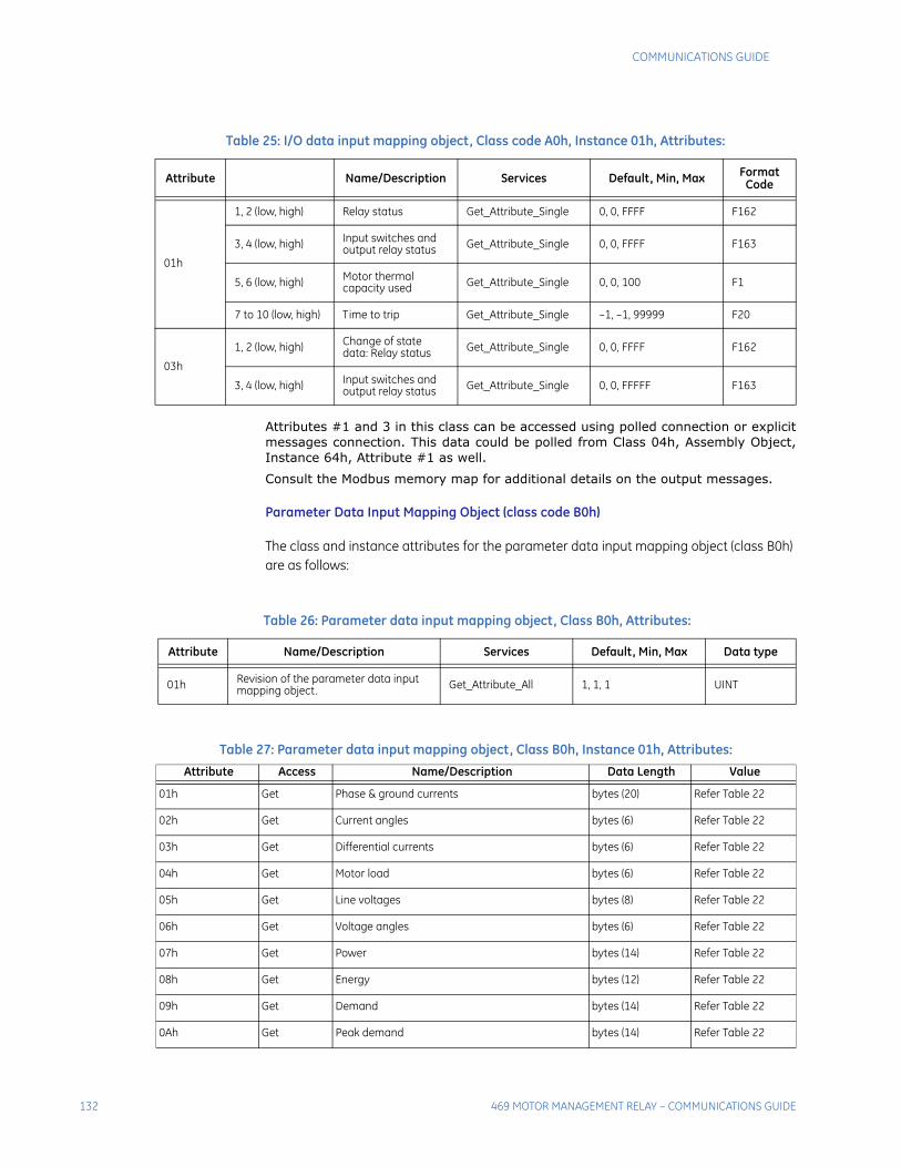
132 469 MOTOR MANAGEMENT RELAY – COMMUNICATIONS GUIDE
COMMUNICATIONS GUIDE
Attributes #1 and 3 in this class can be accessed using polled connection or explicitmessages connection. This data could be polled from Class 04h, Assembly Object,Instance 64h, Attribute #1 as well.
Consult the Modbus memory map for additional details on the output messages.
Parameter Data Input Mapping Object (class code B0h)
The class and instance attributes for the parameter data input mapping object (class B0h) are as follows:
Table 25: I/O data input mapping object, Class code A0h, Instance 01h, Attributes:
Attribute Name/Description Services Default, Min, Max Format Code
01h
1, 2 (low, high) Relay status Get_Attribute_Single 0, 0, FFFF F162
3, 4 (low, high) Input switches and output relay status Get_Attribute_Single 0, 0, FFFF F163
5, 6 (low, high) Motor thermal capacity used Get_Attribute_Single 0, 0, 100 F1
7 to 10 (low, high) Time to trip Get_Attribute_Single –1, –1, 99999 F20
03h
1, 2 (low, high) Change of state data: Relay status Get_Attribute_Single 0, 0, FFFF F162
3, 4 (low, high) Input switches and output relay status Get_Attribute_Single 0, 0, FFFFF F163
Table 26: Parameter data input mapping object, Class B0h, Attributes:
Attribute Name/Description Services Default, Min, Max Data type
01h Revision of the parameter data input mapping object. Get_Attribute_All 1, 1, 1 UINT
Table 27: Parameter data input mapping object, Class B0h, Instance 01h, Attributes:
Attribute Access Name/Description Data Length Value
01h Get Phase & ground currents bytes (20) Refer Table 22
02h Get Current angles bytes (6) Refer Table 22
03h Get Differential currents bytes (6) Refer Table 22
04h Get Motor load bytes (6) Refer Table 22
05h Get Line voltages bytes (8) Refer Table 22
06h Get Voltage angles bytes (6) Refer Table 22
07h Get Power bytes (14) Refer Table 22
08h Get Energy bytes (12) Refer Table 22
09h Get Demand bytes (14) Refer Table 22
0Ah Get Peak demand bytes (14) Refer Table 22
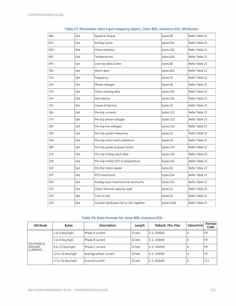
COMMUNICATIONS GUIDE
469 MOTOR MANAGEMENT RELAY – COMMUNICATIONS GUIDE 133
0Bh Get Speed & Torque bytes (8) Refer Table 22
0Ch Get Analog inputs bytes (24) Refer Table 22
0Dh Get Motor statistics bytes (16) Refer Table 22
0Eh Get Temperatures bytes (24) Refer Table 22
0Fh Get Last trip date & time bytes (8) Refer Table 22
10h Get Alarm data bytes (62) Refer Table 22
11h Get Frequency bytes (2) Refer Table 22
12h Get Phase voltages bytes (8) Refer Table 22
13h Get Motor starting data bytes (16) Refer Table 22
14h Get Start blocks bytes (10) Refer Table 22
15h Get Cause of last trip bytes (2) Refer Table 22
16h Get Pre-trip currents bytes (22) Refer Table 22
17h Get Pre-trip phase voltages bytes (12) Refer Table 22
18h Get Pre-trip line voltages bytes (12) Refer Table 22
19h Get Pre-trip system frequency bytes (2) Refer Table 22
1Ah Get Pre-trip motor load unbalance bytes (4) Refer Table 22
1Bh Get Pre-trip power & power factor bytes (12) Refer Table 22
1Ch Get Pre-trip analog input data bytes (16) Refer Table 22
1Dh Get Pre-trip hottest RTD & temperature bytes (16) Refer Table 22
1Eh Get Pre-trip motor speed bytes (4) Refer Table 22
1Fh Get RTD maximums bytes (24) Refer Table 22
20h Get Analog input maximums & minimums bytes (32) Refer Table 22
21h Get Motor thermal capacity used bytes (2) Refer Table 22
22h Get Time to trip bytes (4) Refer Table 22
23h Get Contain attributes 01h to 10h together bytes (248) Refer Table 22
Table 27: Parameter data input mapping object, Class B0h, Instance 01h, Attributes:
Table 28: Data formats for class B0h, Instance 01h:
Attribute Bytes Description Length Default, Min, Max Value/Unit Format Code
01h PHASE & GROUND CURRENTS
1 to 4 (low,high) Phase A current 32 bits 0, 0, 100000 A F9
5 to 8 (low,high) Phase B current 32 bits 0, 0, 100000 A F9
9 to 12 (low,high) Phase C current 32 bits 0, 0, 100000 A F9
13 to 16 (low,high) Average phase current 32 bits 0, 0, 100000 A F9
17 to 20 (low,high) Ground current 32 bits 0, 0, 500000 A F11
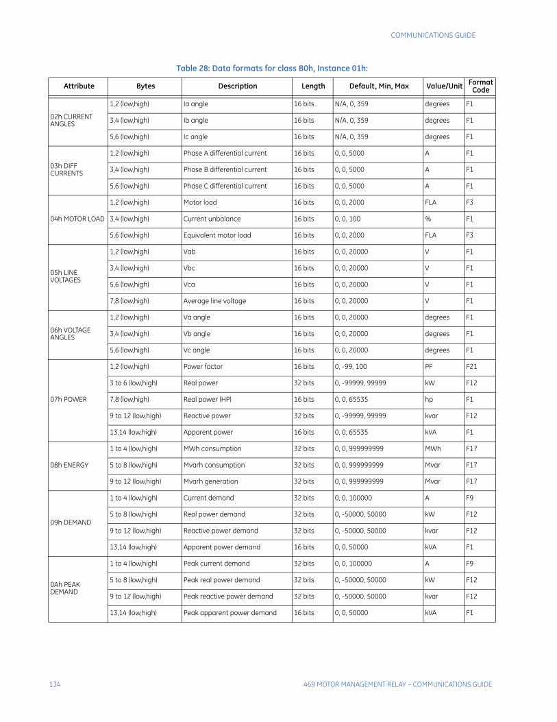
134 469 MOTOR MANAGEMENT RELAY – COMMUNICATIONS GUIDE
COMMUNICATIONS GUIDE
02h CURRENT ANGLES
1,2 (low,high) Ia angle 16 bits N/A, 0, 359 degrees F1
3,4 (low,high) Ib angle 16 bits N/A, 0, 359 degrees F1
5,6 (low,high) Ic angle 16 bits N/A, 0, 359 degrees F1
03h DIFF CURRENTS
1,2 (low,high) Phase A differential current 16 bits 0, 0, 5000 A F1
3,4 (low,high) Phase B differential current 16 bits 0, 0, 5000 A F1
5,6 (low,high) Phase C differential current 16 bits 0, 0, 5000 A F1
04h MOTOR LOAD
1,2 (low,high) Motor load 16 bits 0, 0, 2000 FLA F3
3,4 (low,high) Current unbalance 16 bits 0, 0, 100 % F1
5,6 (low,high) Equivalent motor load 16 bits 0, 0, 2000 FLA F3
05h LINE VOLTAGES
1,2 (low,high) Vab 16 bits 0, 0, 20000 V F1
3,4 (low,high) Vbc 16 bits 0, 0, 20000 V F1
5,6 (low,high) Vca 16 bits 0, 0, 20000 V F1
7,8 (low,high) Average line voltage 16 bits 0, 0, 20000 V F1
06h VOLTAGE ANGLES
1,2 (low,high) Va angle 16 bits 0, 0, 20000 degrees F1
3,4 (low,high) Vb angle 16 bits 0, 0, 20000 degrees F1
5,6 (low,high) Vc angle 16 bits 0, 0, 20000 degrees F1
07h POWER
1,2 (low,high) Power factor 16 bits 0, -99, 100 PF F21
3 to 6 (low,high) Real power 32 bits 0, -99999, 99999 kW F12
7,8 (low,high) Real power (HP) 16 bits 0, 0, 65535 hp F1
9 to 12 (low,high) Reactive power 32 bits 0, -99999, 99999 kvar F12
13,14 (low,high) Apparent power 16 bits 0, 0, 65535 kVA F1
08h ENERGY
1 to 4 (low,high) MWh consumption 32 bits 0, 0, 999999999 MWh F17
5 to 8 (low,high) Mvarh consumption 32 bits 0, 0, 999999999 Mvar F17
9 to 12 (low,high) Mvarh generation 32 bits 0, 0, 999999999 Mvar F17
09h DEMAND
1 to 4 (low,high) Current demand 32 bits 0, 0, 100000 A F9
5 to 8 (low,high) Real power demand 32 bits 0, -50000, 50000 kW F12
9 to 12 (low,high) Reactive power demand 32 bits 0, -50000, 50000 kvar F12
13,14 (low,high) Apparent power demand 16 bits 0, 0, 50000 kVA F1
0Ah PEAK DEMAND
1 to 4 (low,high) Peak current demand 32 bits 0, 0, 100000 A F9
5 to 8 (low,high) Peak real power demand 32 bits 0, -50000, 50000 kW F12
9 to 12 (low,high) Peak reactive power demand 32 bits 0, -50000, 50000 kvar F12
13,14 (low,high) Peak apparent power demand 16 bits 0, 0, 50000 kVA F1
Table 28: Data formats for class B0h, Instance 01h:
Attribute Bytes Description Length Default, Min, Max Value/Unit Format Code
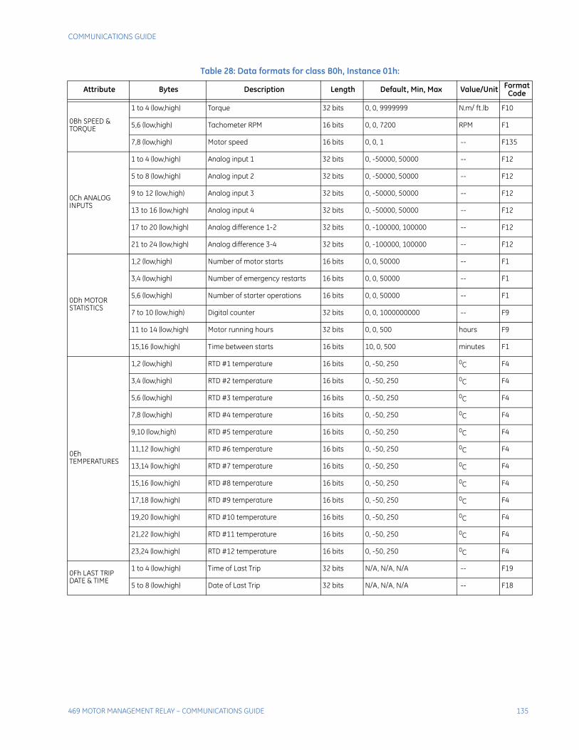
COMMUNICATIONS GUIDE
469 MOTOR MANAGEMENT RELAY – COMMUNICATIONS GUIDE 135
0Bh SPEED & TORQUE
1 to 4 (low,high) Torque 32 bits 0, 0, 9999999 N.m/ ft.lb F10
5,6 (low,high) Tachometer RPM 16 bits 0, 0, 7200 RPM F1
7,8 (low,high) Motor speed 16 bits 0, 0, 1 -- F135
0Ch ANALOG INPUTS
1 to 4 (low,high) Analog input 1 32 bits 0, -50000, 50000 -- F12
5 to 8 (low,high) Analog input 2 32 bits 0, -50000, 50000 -- F12
9 to 12 (low,high) Analog input 3 32 bits 0, -50000, 50000 -- F12
13 to 16 (low,high) Analog input 4 32 bits 0, -50000, 50000 -- F12
17 to 20 (low,high) Analog difference 1-2 32 bits 0, -100000, 100000 -- F12
21 to 24 (low,high) Analog difference 3-4 32 bits 0, -100000, 100000 -- F12
0Dh MOTOR STATISTICS
1,2 (low,high) Number of motor starts 16 bits 0, 0, 50000 -- F1
3,4 (low,high) Number of emergency restarts 16 bits 0, 0, 50000 -- F1
5,6 (low,high) Number of starter operations 16 bits 0, 0, 50000 -- F1
7 to 10 (low,high) Digital counter 32 bits 0, 0, 1000000000 -- F9
11 to 14 (low,high) Motor running hours 32 bits 0, 0, 500 hours F9
15,16 (low,high) Time between starts 16 bits 10, 0, 500 minutes F1
0Eh TEMPERATURES
1,2 (low,high) RTD #1 temperature 16 bits 0, -50, 250 0C F4
3,4 (low,high) RTD #2 temperature 16 bits 0, -50, 250 0C F4
5,6 (low,high) RTD #3 temperature 16 bits 0, -50, 250 0C F4
7,8 (low,high) RTD #4 temperature 16 bits 0, -50, 250 0C F4
9,10 (low,high) RTD #5 temperature 16 bits 0, -50, 250 0C F4
11,12 (low,high) RTD #6 temperature 16 bits 0, -50, 250 0C F4
13,14 (low,high) RTD #7 temperature 16 bits 0, -50, 250 0C F4
15,16 (low,high) RTD #8 temperature 16 bits 0, -50, 250 0C F4
17,18 (low,high) RTD #9 temperature 16 bits 0, -50, 250 0C F4
19,20 (low,high) RTD #10 temperature 16 bits 0, -50, 250 0C F4
21,22 (low,high) RTD #11 temperature 16 bits 0, -50, 250 0C F4
23,24 (low,high) RTD #12 temperature 16 bits 0, -50, 250 0C F4
0Fh LAST TRIP DATE & TIME
1 to 4 (low,high) Time of Last Trip 32 bits N/A, N/A, N/A -- F19
5 to 8 (low,high) Date of Last Trip 32 bits N/A, N/A, N/A -- F18
Table 28: Data formats for class B0h, Instance 01h:
Attribute Bytes Description Length Default, Min, Max Value/Unit Format Code
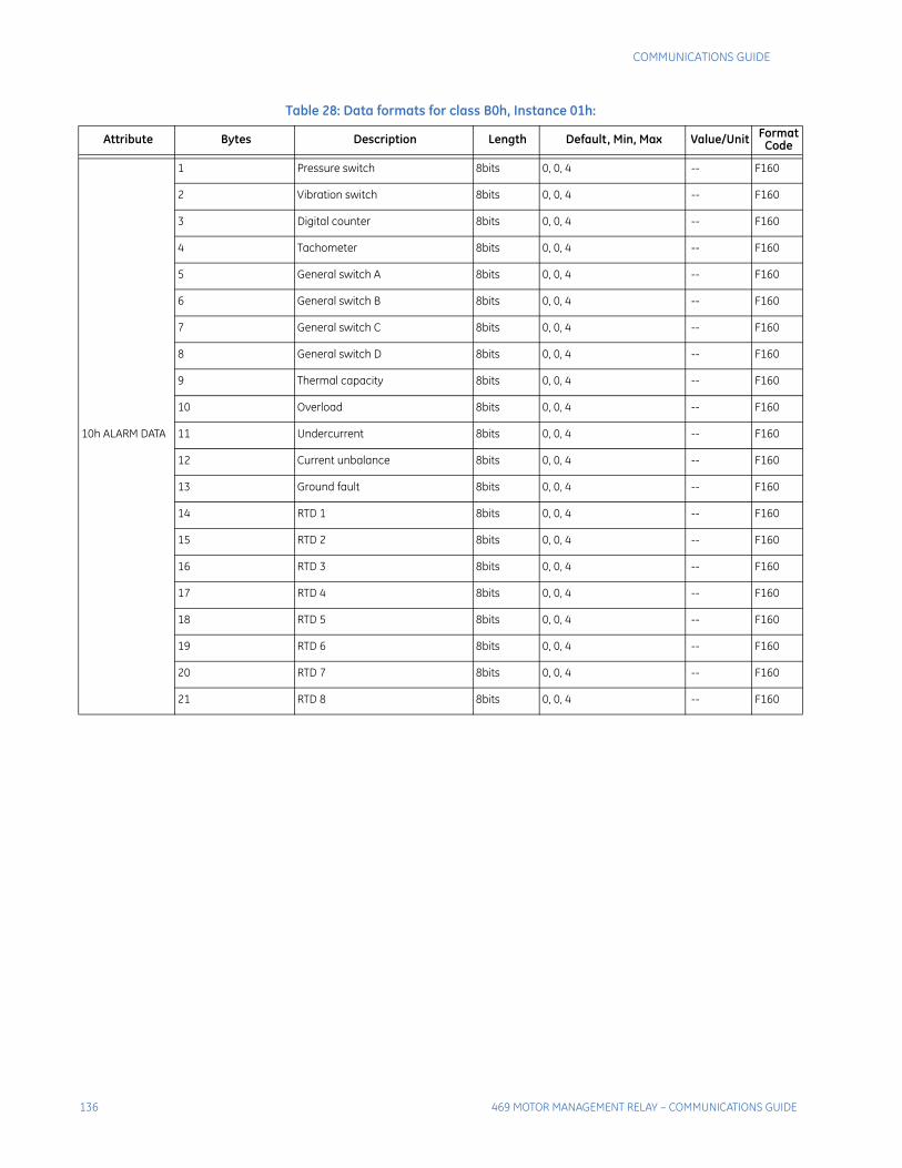
136 469 MOTOR MANAGEMENT RELAY – COMMUNICATIONS GUIDE
COMMUNICATIONS GUIDE
10h ALARM DATA
1 Pressure switch 8bits 0, 0, 4 -- F160
2 Vibration switch 8bits 0, 0, 4 -- F160
3 Digital counter 8bits 0, 0, 4 -- F160
4 Tachometer 8bits 0, 0, 4 -- F160
5 General switch A 8bits 0, 0, 4 -- F160
6 General switch B 8bits 0, 0, 4 -- F160
7 General switch C 8bits 0, 0, 4 -- F160
8 General switch D 8bits 0, 0, 4 -- F160
9 Thermal capacity 8bits 0, 0, 4 -- F160
10 Overload 8bits 0, 0, 4 -- F160
11 Undercurrent 8bits 0, 0, 4 -- F160
12 Current unbalance 8bits 0, 0, 4 -- F160
13 Ground fault 8bits 0, 0, 4 -- F160
14 RTD 1 8bits 0, 0, 4 -- F160
15 RTD 2 8bits 0, 0, 4 -- F160
16 RTD 3 8bits 0, 0, 4 -- F160
17 RTD 4 8bits 0, 0, 4 -- F160
18 RTD 5 8bits 0, 0, 4 -- F160
19 RTD 6 8bits 0, 0, 4 -- F160
20 RTD 7 8bits 0, 0, 4 -- F160
21 RTD 8 8bits 0, 0, 4 -- F160
Table 28: Data formats for class B0h, Instance 01h:
Attribute Bytes Description Length Default, Min, Max Value/Unit Format Code
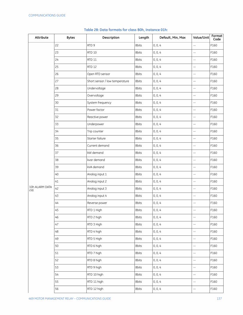
COMMUNICATIONS GUIDE
469 MOTOR MANAGEMENT RELAY – COMMUNICATIONS GUIDE 137
10h ALARM DATA ctd.
22 RTD 9 8bits 0, 0, 4 -- F160
23 RTD 10 8bits 0, 0, 4 -- F160
24 RTD 11 8bits 0, 0, 4 -- F160
25 RTD 12 8bits 0, 0, 4 -- F160
26 Open RTD sensor 8bits 0, 0, 4 -- F160
27 Short sensor / low temperature 8bits 0, 0, 4 -- F160
28 Undervoltage 8bits 0, 0, 4 -- F160
29 Overvoltage 8bits 0, 0, 4 -- F160
30 System frequency 8bits 0, 0, 4 -- F160
31 Power factor 8bits 0, 0, 4 -- F160
32 Reactive power 8bits 0, 0, 4 -- F160
33 Underpower 8bits 0, 0, 4 -- F160
34 Trip counter 8bits 0, 0, 4 -- F160
35 Starter failure 8bits 0, 0, 4 -- F160
36 Current demand 8bits 0, 0, 4 -- F160
37 kW demand 8bits 0, 0, 4 -- F160
38 kvar demand 8bits 0, 0, 4 -- F160
39 kVA demand 8bits 0, 0, 4 -- F160
40 Analog input 1 8bits 0, 0, 4 -- F160
41 Analog input 2 8bits 0, 0, 4 -- F160
42 Analog input 3 8bits 0, 0, 4 -- F160
43 Analog input 4 8bits 0, 0, 4 -- F160
44 Reverse power 8bits 0, 0, 4 -- F160
45 RTD 1 High 8bits 0, 0, 4 -- F160
46 RTD 2 high 8bits 0, 0, 4 -- F160
47 RTD 3 High 8bits 0, 0, 4 -- F160
48 RTD 4 high 8bits 0, 0, 4 -- F160
49 RTD 5 High 8bits 0, 0, 4 -- F160
50 RTD 6 high 8bits 0, 0, 4 -- F160
51 RTD 7 high 8bits 0, 0, 4 -- F160
52 RTD 8 high 8bits 0, 0, 4 -- F160
53 RTD 9 high 8bits 0, 0, 4 -- F160
54 RTD 10 high 8bits 0, 0, 4 -- F160
55 RTD 11 high 8bits 0, 0, 4 -- F160
56 RTD 12 high 8bits 0, 0, 4 -- F160
Table 28: Data formats for class B0h, Instance 01h:
Attribute Bytes Description Length Default, Min, Max Value/Unit Format Code
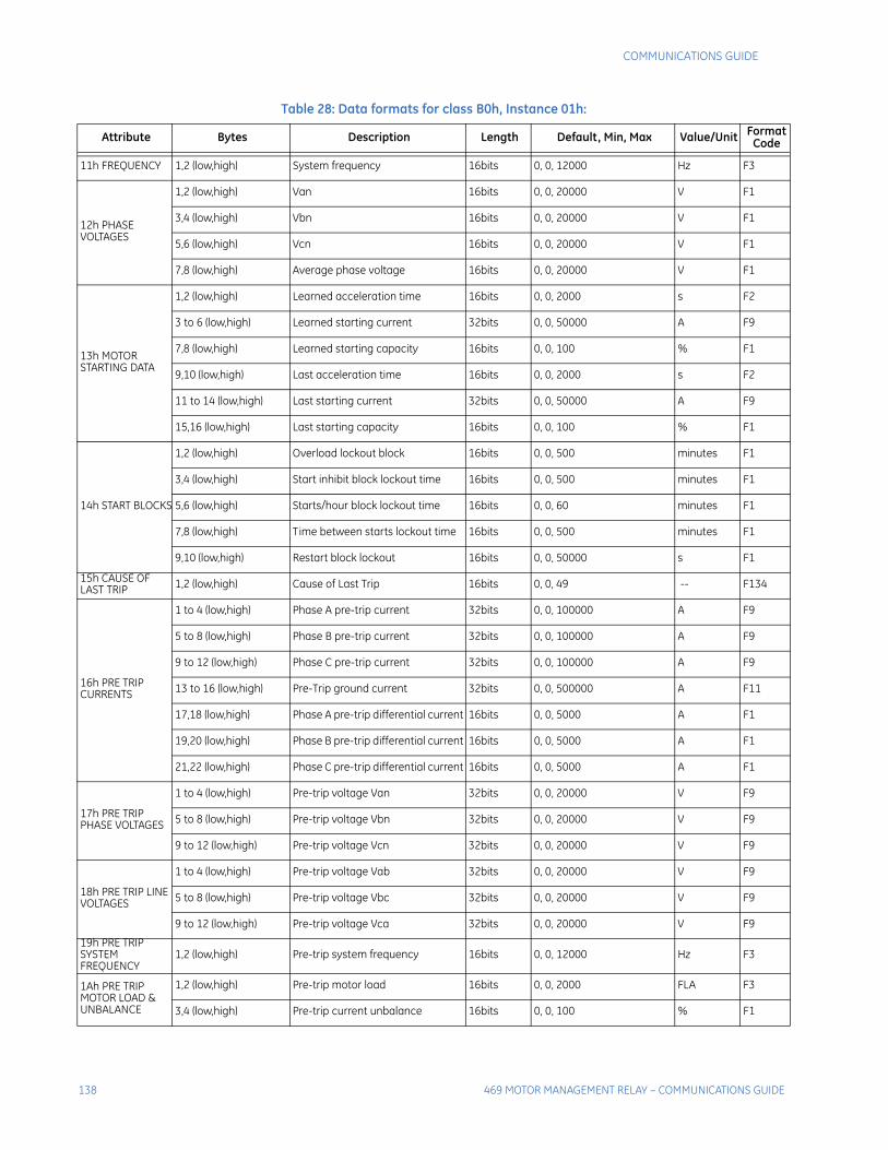
138 469 MOTOR MANAGEMENT RELAY – COMMUNICATIONS GUIDE
COMMUNICATIONS GUIDE
11h FREQUENCY 1,2 (low,high) System frequency 16bits 0, 0, 12000 Hz F3
12h PHASE VOLTAGES
1,2 (low,high) Van 16bits 0, 0, 20000 V F1
3,4 (low,high) Vbn 16bits 0, 0, 20000 V F1
5,6 (low,high) Vcn 16bits 0, 0, 20000 V F1
7,8 (low,high) Average phase voltage 16bits 0, 0, 20000 V F1
13h MOTOR STARTING DATA
1,2 (low,high) Learned acceleration time 16bits 0, 0, 2000 s F2
3 to 6 (low,high) Learned starting current 32bits 0, 0, 50000 A F9
7,8 (low,high) Learned starting capacity 16bits 0, 0, 100 % F1
9,10 (low,high) Last acceleration time 16bits 0, 0, 2000 s F2
11 to 14 (low,high) Last starting current 32bits 0, 0, 50000 A F9
15,16 (low,high) Last starting capacity 16bits 0, 0, 100 % F1
14h START BLOCKS
1,2 (low,high) Overload lockout block 16bits 0, 0, 500 minutes F1
3,4 (low,high) Start inhibit block lockout time 16bits 0, 0, 500 minutes F1
5,6 (low,high) Starts/hour block lockout time 16bits 0, 0, 60 minutes F1
7,8 (low,high) Time between starts lockout time 16bits 0, 0, 500 minutes F1
9,10 (low,high) Restart block lockout 16bits 0, 0, 50000 s F1
15h CAUSE OF LAST TRIP 1,2 (low,high) Cause of Last Trip 16bits 0, 0, 49 -- F134
16h PRE TRIP CURRENTS
1 to 4 (low,high) Phase A pre-trip current 32bits 0, 0, 100000 A F9
5 to 8 (low,high) Phase B pre-trip current 32bits 0, 0, 100000 A F9
9 to 12 (low,high) Phase C pre-trip current 32bits 0, 0, 100000 A F9
13 to 16 (low,high) Pre-Trip ground current 32bits 0, 0, 500000 A F11
17,18 (low,high) Phase A pre-trip differential current 16bits 0, 0, 5000 A F1
19,20 (low,high) Phase B pre-trip differential current 16bits 0, 0, 5000 A F1
21,22 (low,high) Phase C pre-trip differential current 16bits 0, 0, 5000 A F1
17h PRE TRIP PHASE VOLTAGES
1 to 4 (low,high) Pre-trip voltage Van 32bits 0, 0, 20000 V F9
5 to 8 (low,high) Pre-trip voltage Vbn 32bits 0, 0, 20000 V F9
9 to 12 (low,high) Pre-trip voltage Vcn 32bits 0, 0, 20000 V F9
18h PRE TRIP LINE VOLTAGES
1 to 4 (low,high) Pre-trip voltage Vab 32bits 0, 0, 20000 V F9
5 to 8 (low,high) Pre-trip voltage Vbc 32bits 0, 0, 20000 V F9
9 to 12 (low,high) Pre-trip voltage Vca 32bits 0, 0, 20000 V F9
19h PRE TRIP SYSTEM FREQUENCY
1,2 (low,high) Pre-trip system frequency 16bits 0, 0, 12000 Hz F3
1Ah PRE TRIP MOTOR LOAD & UNBALANCE
1,2 (low,high) Pre-trip motor load 16bits 0, 0, 2000 FLA F3
3,4 (low,high) Pre-trip current unbalance 16bits 0, 0, 100 % F1
Table 28: Data formats for class B0h, Instance 01h:
Attribute Bytes Description Length Default, Min, Max Value/Unit Format Code
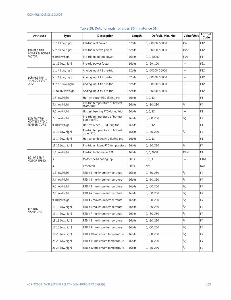
COMMUNICATIONS GUIDE
469 MOTOR MANAGEMENT RELAY – COMMUNICATIONS GUIDE 139
1Bh PRE TRIP POWER & POWER FACTOR
1 to 4 (low,high) Pre-trip real power 32bits 0, -50000, 50000 kW F12
5 to 8 (low,high) Pre-trip reactive power 32bits 0, -50000, 50000 kvar F12
9,10 (low,high) Pre-trip apparent power 16bits 0, 0, 50000 kVA F1
11,12 (low,high) Pre-trip power factor 16bits 0, -99, 100 -- F21
1Ch PRE TRIP ANALOG INPUT DATA
1 to 4 (low,high) Analog input #1 pre-trip 32bits 0, -50000, 50000 -- F12
5 to 8 (low,high) Analog input #2 pre-trip 32bits 0, -50000, 50000 -- F12
9 to 12 (low,high) Analog input #3 pre-trip 32bits 0, -50000, 50000 -- F12
13 to 16 (low,high) Analog input #4 pre-trip 32bits 0, -50000, 50000 -- F12
1Dh PRI TRIP HOTTEST RTD & TEMPERATURE
1,2 (low,high) Hottest stator RTD during trip 16bits 0, 0, 12 -- F1
3,4 (low,high) Pre-trip temperature of hottest stator RTD 16bits 0, -50, 250 0C F4
5,6 (low,high) Hottest bearing RTD during trip 16bits 0, 0, 12 -- F1
7,8 (low,high) Pre-trip temperature of hottest bearing RTD 16bits 0, -50, 250 0C F4
9,10 (low,high) Hottest other RTD during trip 16bits 0, 0, 12 -- F1
11,12 (low,high) Pre-trip temperature of hottest other RTD 16bits 0, -50, 250 0C F4
13,14 (low,high) Hottest ambient RTD during trip 16bits 0, 0, 12 -- F1
15,16 (low,high) Pre-trip ambient RTD temperature 16bits 0, -50, 250 0C F4
1Eh PRE TRIP MOTOR SPEED
1,2 (low,high) Pre-trip tachometer RPM 16bits 0, 0, 3600 RPM F1
3 Motor speed during trip 8bits 0, 0, 1 -- F161
4 Reserved 8bits N/A -- N/A
1Fh RTD MAXIMUMS
1,2 (low,high) RTD #1 maximum temperature 16bits 0, -50, 250 0C F4
3,4 (low,high) RTD #2 maximum temperature 16bits 0, -50, 250 0C F4
5,6 (low,high) RTD #3 maximum temperature 16bits 0, -50, 250 0C F4
7,8 (low,high) RTD #4 maximum temperature 16bits 0, -50, 250 0C F4
9,10 (low,high) RTD #5 maximum temperature 16bits 0, -50, 250 0C F4
11,12 (low,high) RTD #6 maximum temperature 16bits 0, -50, 250 0C F4
13,14 (low,high) RTD #7 maximum temperature 16bits 0, -50, 250 0C F4
15,16 (low,high) RTD #8 maximum temperature 16bits 0, -50, 250 0C F4
17,18 (low,high) RTD #9 maximum temperature 16bits 0, -50, 250 0C F4
19,20 (low,high) RTD #10 maximum temperature 16bits 0, -50, 250 0C F4
21,22 (low,high) RTD #11 maximum temperature 16bits 0, -50, 250 0C F4
23,24 (low,high) RTD #12 maximum temperature 16bits 0, -50, 250 0C F4
Table 28: Data formats for class B0h, Instance 01h:
Attribute Bytes Description Length Default, Min, Max Value/Unit Format Code
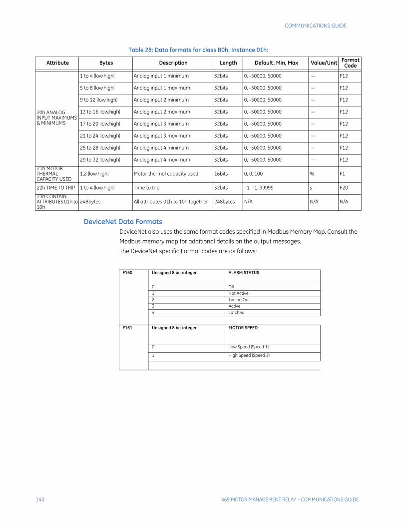
140 469 MOTOR MANAGEMENT RELAY – COMMUNICATIONS GUIDE
COMMUNICATIONS GUIDE
DeviceNet Data FormatsDeviceNet also uses the same format codes specified in Modbus Memory Map. Consult the
Modbus memory map for additional details on the output messages.
The DeviceNet specific Format codes are as follows:
20h ANALOG INPUT MAXIMUMS & MINIMUMS
1 to 4 (low,high) Analog input 1 minimum 32bits 0, -50000, 50000 -- F12
5 to 8 (low,high) Analog input 1 maximum 32bits 0, -50000, 50000 -- F12
9 to 12 (low,high) Analog input 2 minimum 32bits 0, -50000, 50000 -- F12
13 to 16 (low,high) Analog input 2 maximum 32bits 0, -50000, 50000 -- F12
17 to 20 (low,high) Analog input 3 minimum 32bits 0, -50000, 50000 -- F12
21 to 24 (low,high) Analog input 3 maximum 32bits 0, -50000, 50000 -- F12
25 to 28 (low,high) Analog input 4 minimum 32bits 0, -50000, 50000 -- F12
29 to 32 (low,high) Analog input 4 maximum 32bits 0, -50000, 50000 -- F12
21h MOTOR THERMAL CAPACITY USED
1,2 (low,high) Motor thermal capacity used 16bits 0, 0, 100 % F1
22h TIME TO TRIP 1 to 4 (low,high) Time to trip 32bits –1, –1, 99999 s F20
23h CONTAIN ATTRIBUTES 01h to 10h
248bytes All attributes 01h to 10h together 248bytes N/A N/A N/A
Table 28: Data formats for class B0h, Instance 01h:
Attribute Bytes Description Length Default, Min, Max Value/Unit Format Code
F160 Unsigned 8 bit integer ALARM STATUS
0 Off 1 Not Active 2 Timing Out 3 Active 4 Latched
F161 Unsigned 8 bit integer MOTOR SPEED
0 Low Speed (Speed 1)
1 High Speed (Speed 2)
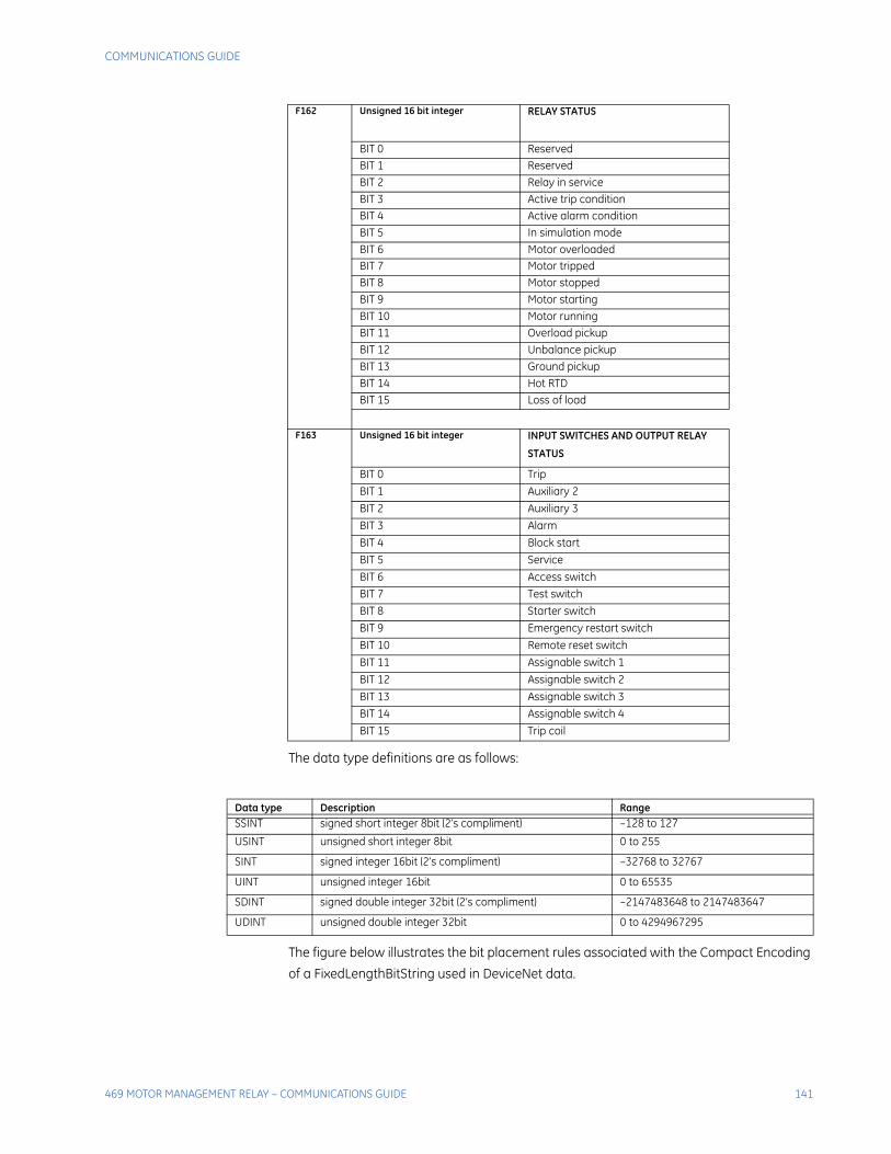
COMMUNICATIONS GUIDE
469 MOTOR MANAGEMENT RELAY – COMMUNICATIONS GUIDE 141
The data type definitions are as follows:
The figure below illustrates the bit placement rules associated with the Compact Encoding
of a FixedLengthBitString used in DeviceNet data.
F162 Unsigned 16 bit integer RELAY STATUS
BIT 0 Reserved BIT 1 Reserved BIT 2 Relay in service BIT 3 Active trip condition BIT 4 Active alarm condition BIT 5 In simulation mode BIT 6 Motor overloaded BIT 7 Motor tripped BIT 8 Motor stopped BIT 9 Motor starting BIT 10 Motor running BIT 11 Overload pickup BIT 12 Unbalance pickup BIT 13 Ground pickup BIT 14 Hot RTD BIT 15 Loss of load
F163 Unsigned 16 bit integer INPUT SWITCHES AND OUTPUT RELAY
STATUS
BIT 0 Trip
BIT 1 Auxiliary 2
BIT 2 Auxiliary 3
BIT 3 Alarm
BIT 4 Block start
BIT 5 Service
BIT 6 Access switch BIT 7 Test switch
BIT 8 Starter switch
BIT 9 Emergency restart switch
BIT 10 Remote reset switch
BIT 11 Assignable switch 1
BIT 12 Assignable switch 2
BIT 13 Assignable switch 3
BIT 14 Assignable switch 4
BIT 15 Trip coil
Data type Description Range SSINT signed short integer 8bit (2’s compliment) –128 to 127
USINT unsigned short integer 8bit 0 to 255
SINT signed integer 16bit (2’s compliment) –32768 to 32767
UINT unsigned integer 16bit 0 to 65535
SDINT signed double integer 32bit (2’s compliment) –2147483648 to 2147483647
UDINT unsigned double integer 32bit 0 to 4294967295
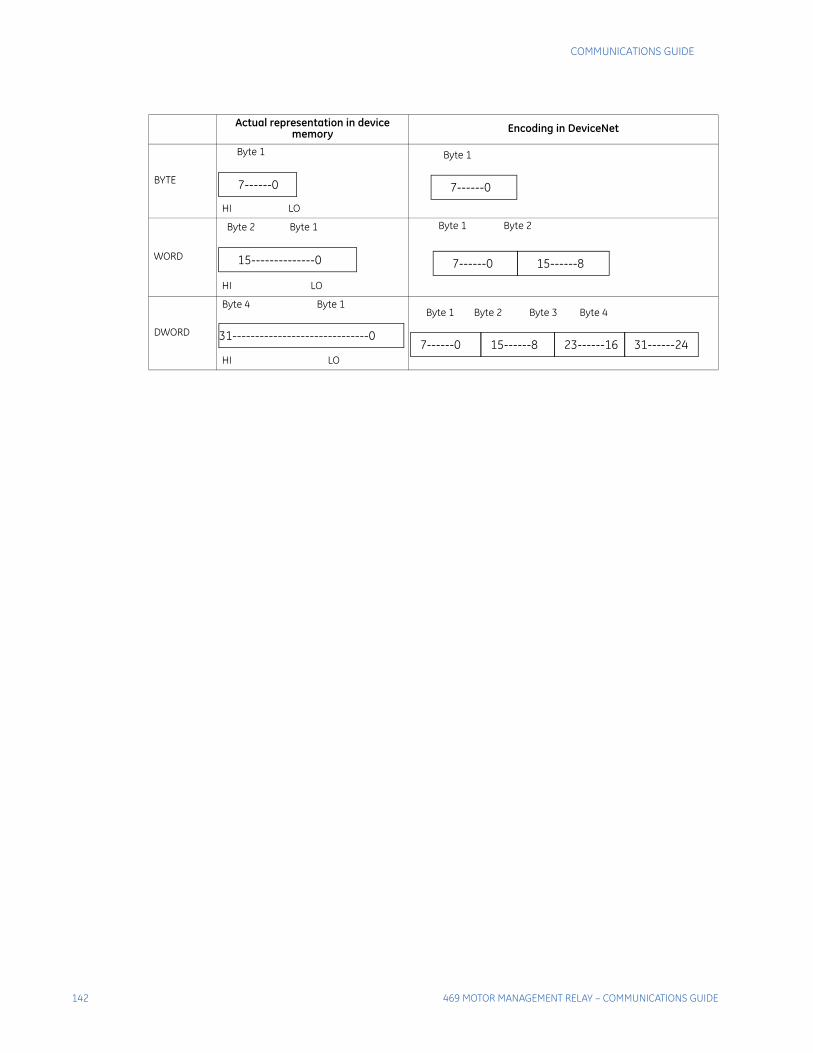
142 469 MOTOR MANAGEMENT RELAY – COMMUNICATIONS GUIDE
COMMUNICATIONS GUIDE
Actual representation in device memory Encoding in DeviceNet
BYTE
Byte 1
HI LO
Byte 1
WORD
Byte 2 Byte 1
HI LO
Byte 1 Byte 2
DWORD
Byte 4 Byte 1
HI LO
Byte 1 Byte 2 Byte 3 Byte 4
7------0 7------0
15--------------0 7------0 15------8
31------------------------------07------0 15------8 23------16 31------24
469 MOTOR MANAGEMENT RELAY – COMMUNICATIONS GUIDE CGI-1
Index
A
ACCELERATION TIMER ......................................................50ACTUAL VALUES, READING ................................................ 7ANALOG INPUT 1 ...............................................................66ANALOG INPUT 1-2 DIFFERENCE ......................................73ANALOG INPUT 2 ...............................................................67ANALOG INPUT 3 ...............................................................68ANALOG INPUT 3-4 DIFFERENCE ......................................74ANALOG INPUT 4 ...............................................................69ANALOG INPUTS .......................................................... 31, 33ANALOG OUTPUTS.............................................................63ASSIGNABLE INPUTS .........................................................41AVERAGE MOTOR LOAD ....................................................32
C
CLEAR DATA ......................................................................40COMMANDS .......................................................................19COMMUNICATIONS ............................................................35CRC-16 .............................................................................2, 3CURRENT DEMAND ............................................................62CURRENT METERING.........................................................29CURRENT SENSING ...........................................................40CURRENT UNBALANCE ......................................................49CYCLIC REDUNDANCY CHECK ........................................... 2
D
DATA FORMATS, MEMORY MAP ......................................109DATA FRAME FORMAT ........................................................ 2DATA PACKET FORMAT ...................................................... 2DATA RATE ......................................................................... 2DEFAULT MESSAGES ........................................................37DEMAND .............................................................................62DEMAND METERING ..........................................................31DEVICENET
469 specific objects .........................................................131acknowledge handler object .............................................130assembly object ..............................................................127connection object ............................................................128description ......................................................................124DeviceNet object .............................................................126identity object .................................................................125message router object .....................................................126Modbus registers...............................................................36
DIGITAL COUNTERS...........................................................43DIGITAL INPUTS .................................................................29
E
ELECTRICAL INTERFACE .................................................... 1ERROR CHECKING .............................................................. 2ERROR RESPONSES ..........................................................12ETHERNET .........................................................................36EVENT RECORD
CGI-2 469 MOTOR MANAGEMENT RELAY – COMMUNICATIONS GUIDE
memory map locations ...................................................... 15EVENT RECORDER
memory map locations ...................................................... 15Modbus registers .............................................................. 74
F
FAULT VALUES .................................................................. 70FORCE OUTPUT RELAYS .................................................. 46FORMAT CODES .............................................................. 109
G
GENERAL COUNTERS ....................................................... 34GENERAL SWITCH A ......................................................... 44GENERAL SWITCH B ......................................................... 45GENERAL SWITCH C ......................................................... 45GENERAL SWITCH D ......................................................... 45GROUND FAULT ................................................................ 49
I
INSTALLATION................................................................... 40
J
JOGGING BLOCK ............................................................... 50
L
LAST TRIP DATA................................................................ 26LOAD SHED TRIP............................................................... 42LOOPBACK TEST ............................................................... 10
M
MECHANICAL JAM ............................................................. 48MEMORY MAP
description ....................................................................... 13format codes .................................................................. 109table ................................................................................ 19user-definable area........................................................... 13
MEMORY MAP FORMAT CODES ...................................... 109MEMORY MAP INFORMATION ........................................... 13MESSAGE SCRATCHPAD .................................................. 37MODBUS
description ......................................................................... 1digital input status .............................................................. 5execute operation ............................................................... 8function code 01 ................................................................. 5function code 02 ............................................................. 5, 6function code 03 ................................................................. 7function code 04 ................................................................. 7function code 05 ................................................................. 8function code 06 ................................................................. 8function code 07 ................................................................. 9function code 08 ............................................................... 10function code 16 ..........................................................10, 11functions ............................................................................ 5
469 MOTOR MANAGEMENT RELAY – COMMUNICATIONS GUIDE CGI-3
loopback test ....................................................................10performing commands .......................................................11read actual values .............................................................. 7read device status .............................................................. 9read relay coil .................................................................... 5read setpoints .................................................................... 7store multiple setpoints......................................................10store single setpoint ........................................................... 8supported functions ............................................................ 5
MODBUS FORMAT CODES ...............................................109MOTOR STARTING .............................................................32MOTOR STATUS .................................................................25
O
OPEN RTD SENSOR ...........................................................56OVERLOAD ALARM ............................................................48OVERLOAD CURVE SETUP ................................................47OVERTORQUE SETUP ........................................................61OVERVOLTAGE ..................................................................58
P
PHASE DIFFERENTIAL .......................................................50PHASE REVERSAL .............................................................59PHASORS ...........................................................................35POWER DEMAND ...............................................................62POWER FACTOR ................................................................59POWER METERING ............................................................31POWER SYSTEM ................................................................41PREFAULT VALUES ............................................................70PRESSURE SWITCH ALARM...............................................43PRESSURE SWITCH TRIP ..................................................43PULSE OUTPUT..................................................................62
R
REACTIVE POWER .............................................................60REAL TIME CLOCK ....................................................... 29, 37REDUCED VOLTAGE ..........................................................41RELAY RESET MODE .........................................................46REMOTE ALARM.................................................................42REMOTE TRIP ....................................................................42RESTART BLOCK ...............................................................51REVERSE POWER ..............................................................60REVISION ...........................................................................19RS232 .................................................................................. 1RS485 .................................................................................. 1RTD #1 ...............................................................................51RTD #10..............................................................................55RTD #11..............................................................................55RTD #12..............................................................................56RTD #2 ...............................................................................51RTD #3 ...............................................................................52RTD #4 ...............................................................................52RTD #5 ...............................................................................53RTD #6 ...............................................................................53RTD #7 ...............................................................................54RTD #8 ...............................................................................54RTD #9 ...............................................................................55RTD HIGH ALARMS ............................................................57RTD MAXIMUMS .................................................................32RTD SHORT/LOW TEMPERATURE......................................57RTD TYPES ........................................................................51
CGI-4 469 MOTOR MANAGEMENT RELAY – COMMUNICATIONS GUIDE
S
SERIAL COMMUNICATIONS CONTROL .............................. 41SERIAL PORTS .................................................................. 36SHORT CIRCUIT TRIP ........................................................ 48SIMULATION MODE ........................................................... 70SPEED ............................................................................... 31SPEED 2 ACCELERATION .................................................. 73SPEED 2 OVERLOAD SETUP ............................................. 71SPEED 2 UNDERCURRENT................................................ 72SPEED SWITCH TRIP......................................................... 42START BLOCKS ................................................................. 28START INHIBIT .................................................................. 50STARTER FAILURE ............................................................ 61STARTER STATUS ............................................................. 41STATUS SETPOINTS.......................................................... 27SUPPORTED MODBUS FUNCTIONS .................................... 5SYSTEM STATUS ............................................................... 26
T
TACHOMETER ................................................................... 44TEMPERATURE ................................................................. 30TEST ANALOG OUTPUTS .................................................. 71TEST OUTPUT RELAYS ..................................................... 71THERMAL MODEL .............................................................. 46TIMERS .............................................................................. 34TIMING................................................................................. 4TORQUE SETUP ................................................................ 61TRACE MEMORY ............................................................... 75TRIP COUNTER ................................................................. 61TRIP COUNTERS ............................................................... 33
U
UNDERCURRENT............................................................... 49UNDERPOWER .................................................................. 60UNDERVOLTAGE ............................................................... 58USER DEFINABLE MEMORY MAP ...................................... 13USER MAP ......................................................................... 19
V
VIBRATION SWITCH ALARM .............................................. 43VIBRATION SWITCH TRIP .................................................. 43VOLTAGE FREQUENCY ..................................................... 59VOLTAGE SENSING ........................................................... 40
W
WAVEFORM CAPTURE ...................................................... 15