Embed Size (px)
Citation preview
@#GEINT&*
GE Internal
1
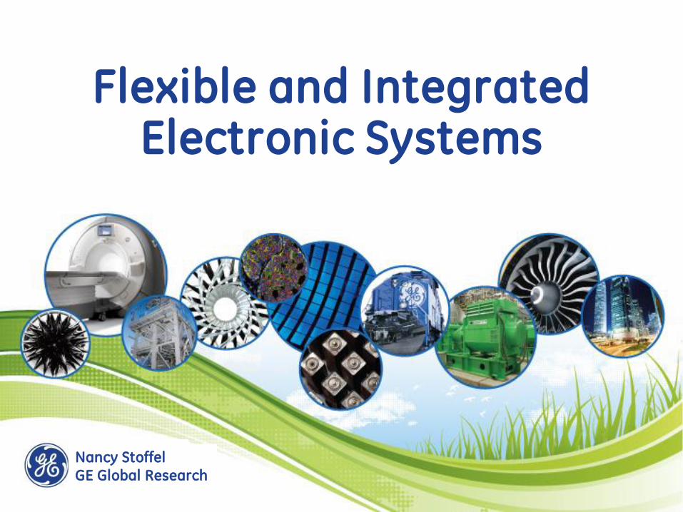
Flexible and Integrated Electronic Systems
Nancy Stoffel
GE Global Research
@#GEINT&*
GE Internal
2
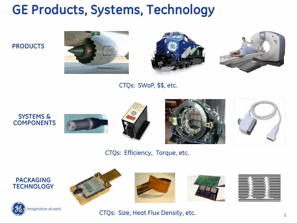
PRODUCTS
SYSTEMS & COMPONENTS
PACKAGING TECHNOLOGY
GE Products, Systems, Technology
CTQs: SWaP, $$, etc.
CTQs: Efficiency, Torque, etc.
CTQs: Size, Heat Flux Density, etc.
@#GEINT&*
GE Internal
3
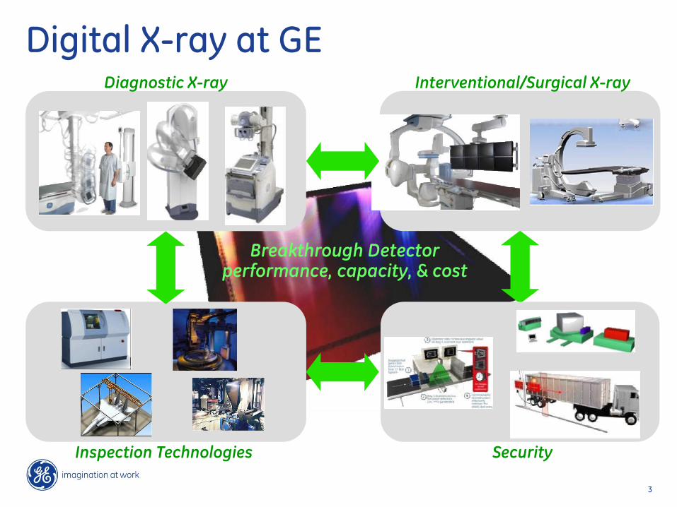
Digital X-ray at GE Diagnostic X-ray Interventional/Surgical X-ray
Security Inspection Technologies
Breakthrough Detector performance, capacity, & cost
@#GEINT&*
GE Internal
4
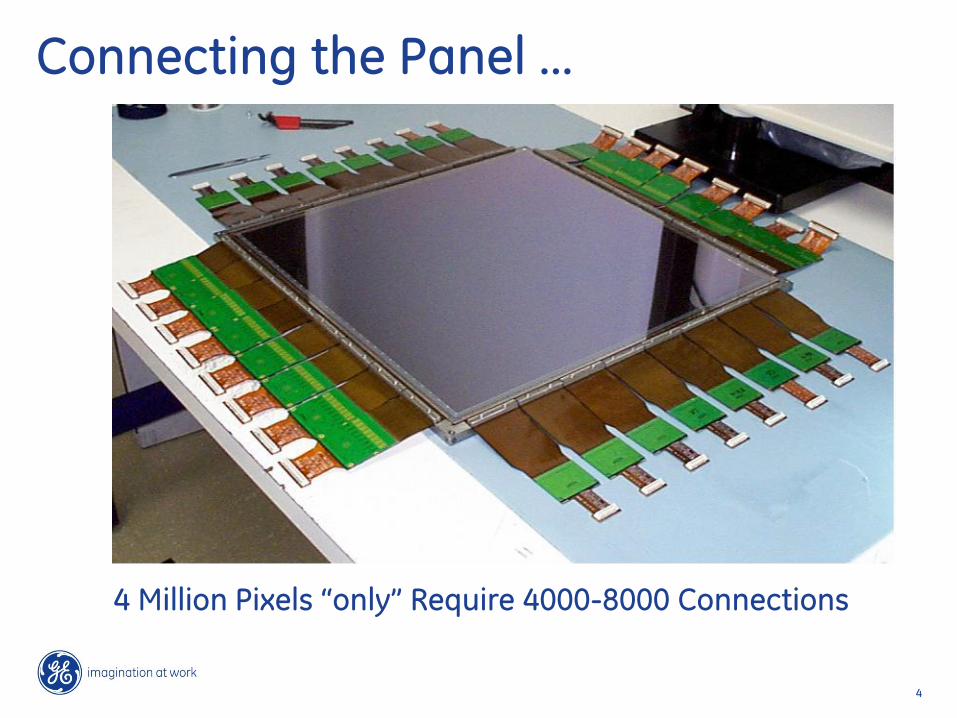
4 Million Pixels “only” Require 4000-8000 Connections
Connecting the Panel …
@#GEINT&*
GE Internal
5
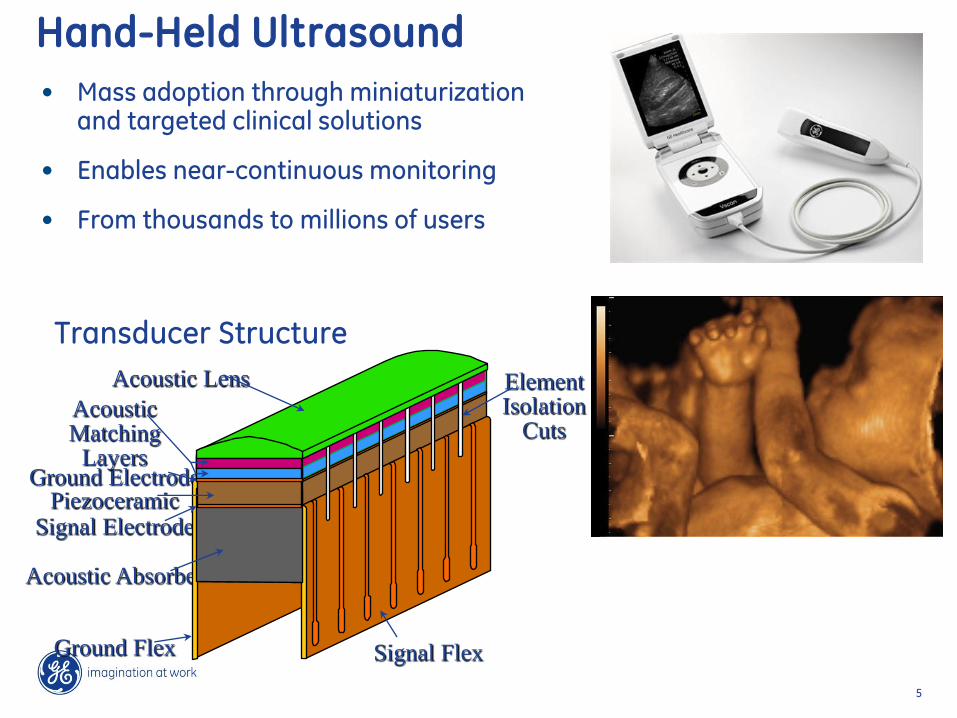
Hand-Held Ultrasound
• Mass adoption through miniaturization and targeted clinical solutions
• Enables near-continuous monitoring
• From thousands to millions of users
Element Isolation
Cuts
Signal Flex Ground Flex
Acoustic Absorber
Signal Electrode Piezoceramic
Ground Electrode
Acoustic Matching
Layers
Acoustic Lens
Transducer Structure
@#GEINT&*
GE Internal
6 6
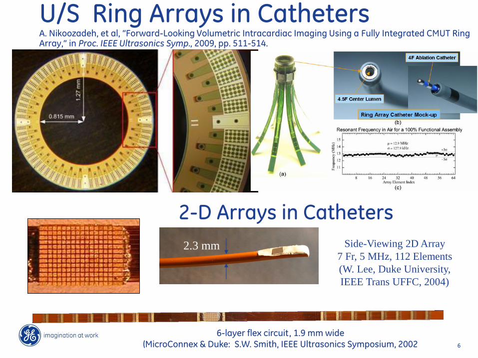
U/S Ring Arrays in Catheters A. Nikoozadeh, et al, “Forward-Looking Volumetric Intracardiac Imaging Using a Fully Integrated CMUT Ring Array,” in Proc. IEEE Ultrasonics Symp., 2009, pp. 511-514.
Nikoozadeh et.al., Stanford
IEEE Ultrasonics Symposium, 2009
2.3 mm Side-Viewing 2D Array
7 Fr, 5 MHz, 112 Elements
(W. Lee, Duke University,
IEEE Trans UFFC, 2004)
2-D Arrays in Catheters
6-layer flex circuit, 1.9 mm wide (MicroConnex & Duke: S.W. Smith, IEEE Ultrasonics Symposium, 2002
@#GEINT&*
GE Internal
7
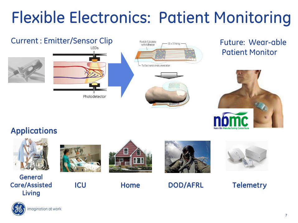
Home Telemetry
Flexible Electronics: Patient Monitoring
Current : Emitter/Sensor Clip Future: Wear-able Patient Monitor
General
Care/Assisted Living
ICU DOD/AFRL
Applications
@#GEINT&*
GE Internal
8
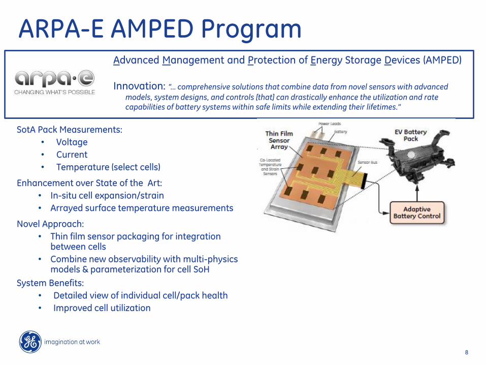
ARPA-E AMPED Program Advanced Management and Protection of Energy Storage Devices (AMPED)
Innovation: “… comprehensive solutions that combine data from novel sensors with advanced
models, system designs, and controls [that] can drastically enhance the utilization and rate capabilities of battery systems within safe limits while extending their lifetimes.”
SotA Pack Measurements:
• Voltage
• Current
• Temperature (select cells)
Enhancement over State of the Art:
• In-situ cell expansion/strain
• Arrayed surface temperature measurements
Novel Approach:
• Thin film sensor packaging for integration between cells
• Combine new observability with multi-physics models & parameterization for cell SoH
System Benefits:
• Detailed view of individual cell/pack health
• Improved cell utilization
@#GEINT&*
GE Internal
9
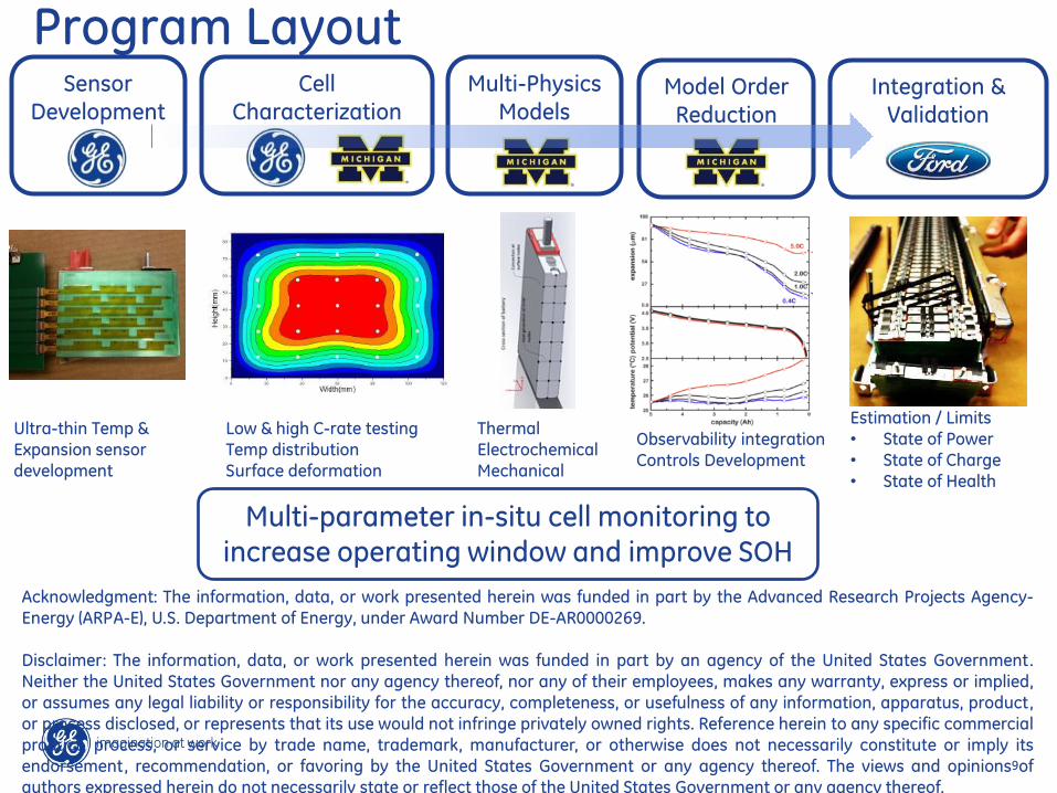
Program Layout
Observability integration Controls Development
Ultra-thin Temp & Expansion sensor development
Thermal Electrochemical Mechanical
Estimation / Limits • State of Power • State of Charge • State of Health
Multi-Physics
Models Model Order
Reduction
Integration & Validation
Cell
Characterization
Sensor
Development
Low & high C-rate testing Temp distribution Surface deformation
Multi-parameter in-situ cell monitoring to increase operating window and improve SOH
Acknowledgment: The information, data, or work presented herein was funded in part by the Advanced Research Projects Agency-Energy (ARPA-E), U.S. Department of Energy, under Award Number DE-AR0000269. Disclaimer: The information, data, or work presented herein was funded in part by an agency of the United States Government.
Neither the United States Government nor any agency thereof, nor any of their employees, makes any warranty, express or implied, or assumes any legal liability or responsibility for the accuracy, completeness, or usefulness of any information, apparatus, product, or process disclosed, or represents that its use would not infringe privately owned rights. Reference herein to any specific commercial product, process, or service by trade name, trademark, manufacturer, or otherwise does not necessarily constitute or imply its endorsement, recommendation, or favoring by the United States Government or any agency thereof. The views and opinions of authors expressed herein do not necessarily state or reflect those of the United States Government or any agency thereof.
@#GEINT&*
GE Internal
10
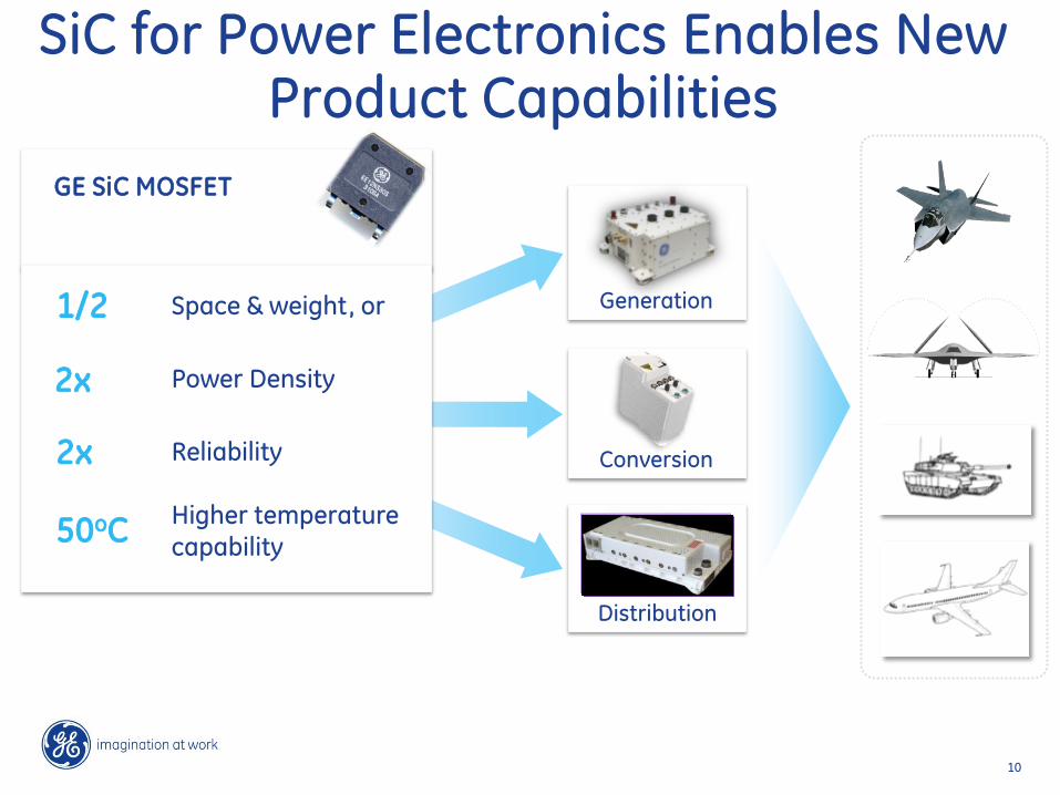
SiC for Power Electronics Enables New Product Capabilities
GE SiC MOSFET
1/2 Space & weight, or
2x
50oC
Reliability
Higher temperature capability
Generation
Conversion
Distribution
Power Density 2x
@#GEINT&*
GE Internal
11
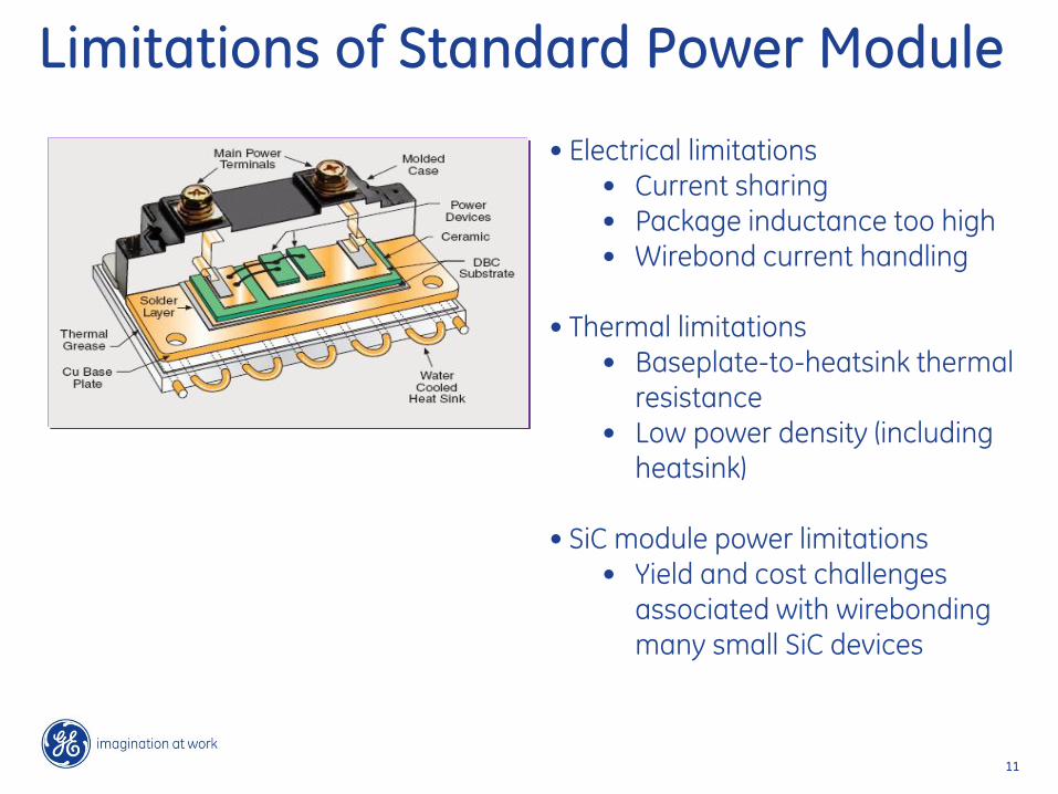
Limitations of Standard Power Module
• Electrical limitations • Current sharing • Package inductance too high • Wirebond current handling
• Thermal limitations • Baseplate-to-heatsink thermal
resistance • Low power density (including
heatsink)
• SiC module power limitations • Yield and cost challenges
associated with wirebonding many small SiC devices
@#GEPUB&*
GE Internal
12
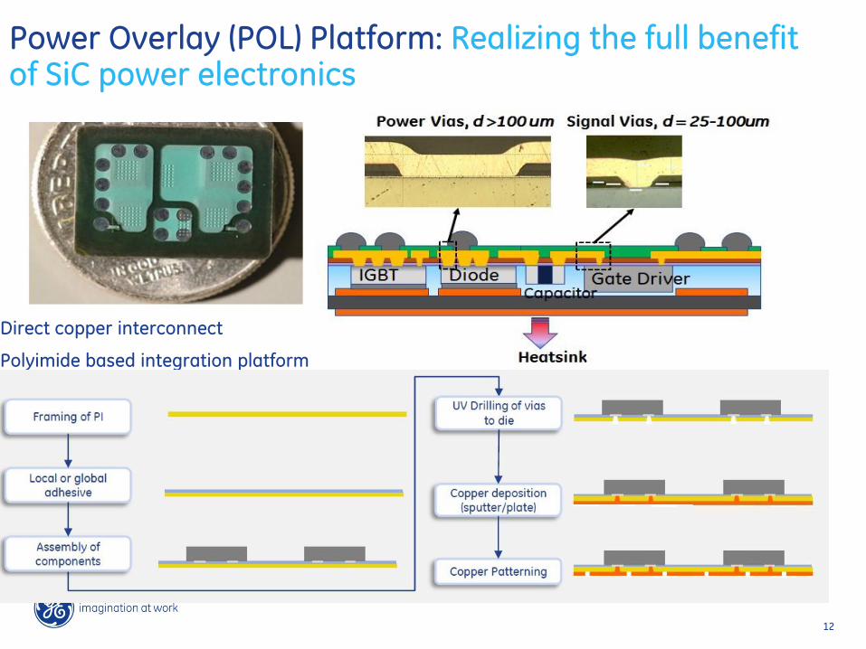
Power Overlay (POL) Platform: Realizing the full benefit of SiC power electronics
Direct copper interconnect
Polyimide based integration platform
@#GEPUB&*
GE Internal
13
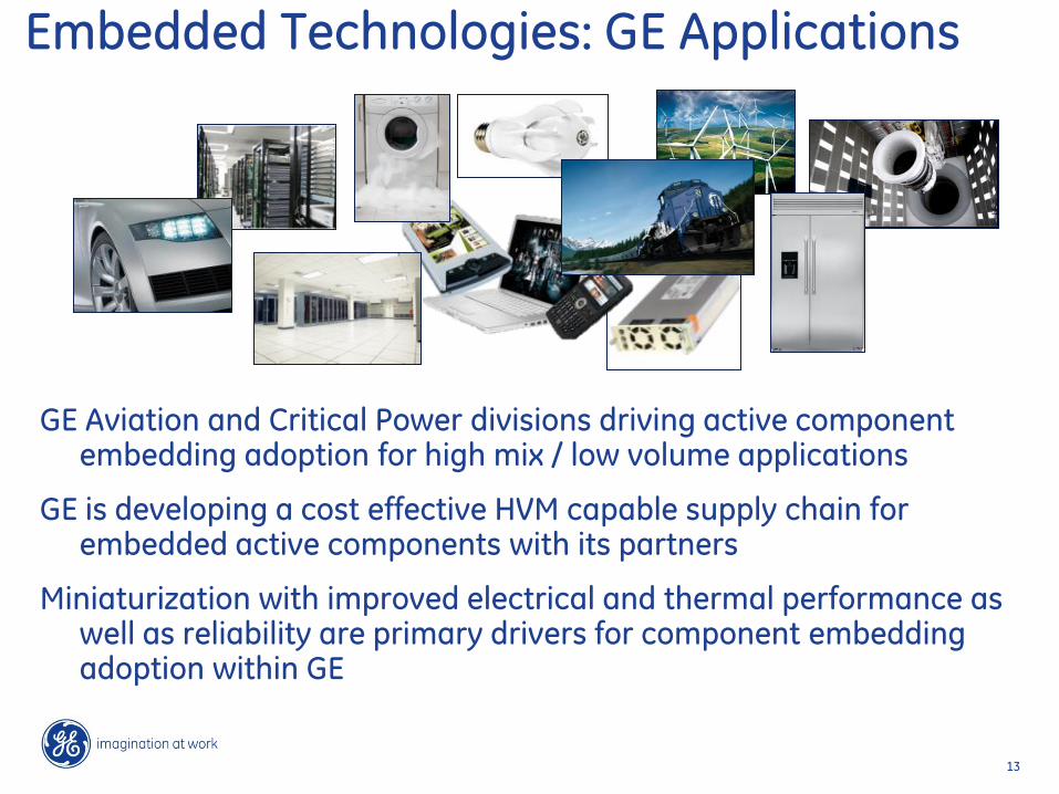
Embedded Technologies: GE Applications
GE Aviation and Critical Power divisions driving active component embedding adoption for high mix / low volume applications
GE is developing a cost effective HVM capable supply chain for embedded active components with its partners
Miniaturization with improved electrical and thermal performance as well as reliability are primary drivers for component embedding adoption within GE
@#GEPUB&*
GE Internal
14
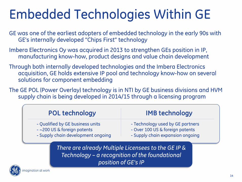
Embedded Technologies Within GE
GE was one of the earliest adopters of embedded technology in the early 90s with GE’s internally developed “Chips First” technology
Imbera Electronics Oy was acquired in 2013 to strengthen GEs position in IP, manufacturing know-how, product designs and value chain development
Through both internally developed technologies and the Imbera Electronics acquisition, GE holds extensive IP pool and technology know-how on several solutions for component embedding
The GE POL (Power Overlay) technology is in NTI by GE business divisions and HVM supply chain is being developed in 2014/15 through a licensing program
IMB technology POL technology
- Qualified by GE business units - ~200 US & foreign patents - Supply chain development ongoing
- Technology used by GE partners - Over 100 US & foreign patents - Supply chain expansion ongoing
There are already Multiple Licensees to the GE IP & Technology – a recognition of the foundational
position of GE’s IP
@#GEPUB&*
GE Internal
15
• Direct Al, Au or Cu land contact
• No need for wafer level RDL
• Thin PI and adhesive layers with minimal
microvia size (35µm)
• Short via with lowest parasitics and best
electrical performance
• Face down C/A with very small die movement
• Zero voiding adhesive layer with excellent process control
• Unique PI processing technology with
exceptional dimensional stability
• Designed and tested up to 3.3kV
• Adaptable in PCB panel-sized manufacturing environment
• Improved manufacturability with high production yield levels
• Meets the required cost levels in consumer electronics
• Technology standardization: GE licensing to multiple manufacturers
Framing of PI
Local or global adhesive
Assembly of components
UV Drilling of vias to die
Copper deposition (sputter/plate)
Copper Patterning
TECHNOLOGY MICROVIA MANUFACTURING
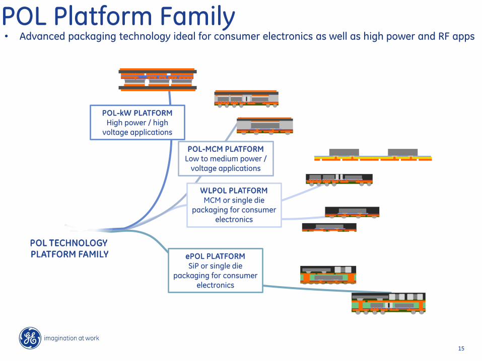
POL Platform Family
POL TECHNOLOGY PLATFORM FAMILY
POL-MCM PLATFORM Low to medium power /
voltage applications
WLPOL PLATFORM MCM or single die
packaging for consumer electronics
ePOL PLATFORM SiP or single die
packaging for consumer electronics
POL-kW PLATFORM High power / high
voltage applications
• Advanced packaging technology ideal for consumer electronics as well as high power and RF apps
@#GEPUB&*
GE Internal
16
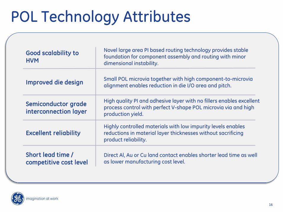
POL Technology Attributes
Improved die design
Good scalability to
HVM
Small POL microvia together with high component-to-microvia alignment enables reduction in die I/O area and pitch.
Novel large area PI based routing technology provides stable foundation for component assembly and routing with minor dimensional instability.
High quality PI and adhesive layer with no fillers enables excellent process control with perfect V-shape POL microvia via and high production yield.
Semiconductor grade
interconnection layer
Highly controlled materials with low impurity levels enables reductions in material layer thicknesses without sacrificing product reliability.
Excellent reliability
Direct Al, Au or Cu land contact enables shorter lead time as well as lower manufacturing cost level.
Short lead time /
competitive cost level
@#GEPUB&*
GE Internal
17
Summary Flex and organic electronics diverse uses within GE Growth driven by need for miniaturization, flexible form factor, performance gains New technology projects are often collaborative involving partners in development and in move to HVM