Embed Size (px)
Citation preview
Gamma LUT v1.0
LogiCORE IP Product Guide
PG285 October 4, 2017

Gamma LUT v1.0 www.xilinx.com 2PG285 October 4, 2017
Table of Contents
IP Facts
Chapter 1: Overview
Feature Summary. . . . . . . . . . . . . . . . . . . . . . . . . . . . . . . . . . . . . . . . . . . . . . . . . . . . . . . . . . . . . . . . . . 6
Applications . . . . . . . . . . . . . . . . . . . . . . . . . . . . . . . . . . . . . . . . . . . . . . . . . . . . . . . . . . . . . . . . . . . . . . 6
Licensing and Ordering . . . . . . . . . . . . . . . . . . . . . . . . . . . . . . . . . . . . . . . . . . . . . . . . . . . . . . . . . . . . . 7
Chapter 2: Product Specification
Standards . . . . . . . . . . . . . . . . . . . . . . . . . . . . . . . . . . . . . . . . . . . . . . . . . . . . . . . . . . . . . . . . . . . . . . . . 8
Performance. . . . . . . . . . . . . . . . . . . . . . . . . . . . . . . . . . . . . . . . . . . . . . . . . . . . . . . . . . . . . . . . . . . . . . 8
Register Space . . . . . . . . . . . . . . . . . . . . . . . . . . . . . . . . . . . . . . . . . . . . . . . . . . . . . . . . . . . . . . . . . . . . 9
Chapter 3: Designing with the Core
General Design Guidelines . . . . . . . . . . . . . . . . . . . . . . . . . . . . . . . . . . . . . . . . . . . . . . . . . . . . . . . . . 18
Clock, Enable, and Reset Considerations . . . . . . . . . . . . . . . . . . . . . . . . . . . . . . . . . . . . . . . . . . . . . . 18
Chapter 4: Design Flow Steps
Customizing and Generating the Core . . . . . . . . . . . . . . . . . . . . . . . . . . . . . . . . . . . . . . . . . . . . . . . . 20
Output Generation. . . . . . . . . . . . . . . . . . . . . . . . . . . . . . . . . . . . . . . . . . . . . . . . . . . . . . . . . . . . . . . . 22
Constraining the Core . . . . . . . . . . . . . . . . . . . . . . . . . . . . . . . . . . . . . . . . . . . . . . . . . . . . . . . . . . . . . 22
Simulation . . . . . . . . . . . . . . . . . . . . . . . . . . . . . . . . . . . . . . . . . . . . . . . . . . . . . . . . . . . . . . . . . . . . . . 23
Synthesis and Implementation . . . . . . . . . . . . . . . . . . . . . . . . . . . . . . . . . . . . . . . . . . . . . . . . . . . . . . 23
Chapter 5: Detailed Example Design
Simulation Example Design . . . . . . . . . . . . . . . . . . . . . . . . . . . . . . . . . . . . . . . . . . . . . . . . . . . . . . . . . 25
Synthesizable Example Design . . . . . . . . . . . . . . . . . . . . . . . . . . . . . . . . . . . . . . . . . . . . . . . . . . . . . . 28
Chapter 6: Test Bench
Appendix A: Verification, Compliance, and Interoperability
Simulation . . . . . . . . . . . . . . . . . . . . . . . . . . . . . . . . . . . . . . . . . . . . . . . . . . . . . . . . . . . . . . . . . . . . . . 33
Hardware Testing. . . . . . . . . . . . . . . . . . . . . . . . . . . . . . . . . . . . . . . . . . . . . . . . . . . . . . . . . . . . . . . . . 33
Interoperability . . . . . . . . . . . . . . . . . . . . . . . . . . . . . . . . . . . . . . . . . . . . . . . . . . . . . . . . . . . . . . . . . . 34
Send Feedback

Gamma LUT v1.0 www.xilinx.com 3PG285 October 4, 2017
Appendix B: Upgrading
Appendix C: Debugging
Finding Help on Xilinx.com . . . . . . . . . . . . . . . . . . . . . . . . . . . . . . . . . . . . . . . . . . . . . . . . . . . . . . . . . 36
Debug Tools . . . . . . . . . . . . . . . . . . . . . . . . . . . . . . . . . . . . . . . . . . . . . . . . . . . . . . . . . . . . . . . . . . . . . 37
Hardware Debug . . . . . . . . . . . . . . . . . . . . . . . . . . . . . . . . . . . . . . . . . . . . . . . . . . . . . . . . . . . . . . . . . 38
Appendix D: Additional Resources
Xilinx Resources . . . . . . . . . . . . . . . . . . . . . . . . . . . . . . . . . . . . . . . . . . . . . . . . . . . . . . . . . . . . . . . . . . 39
Documentation Navigator and Design Hubs . . . . . . . . . . . . . . . . . . . . . . . . . . . . . . . . . . . . . . . . . . . 39
References . . . . . . . . . . . . . . . . . . . . . . . . . . . . . . . . . . . . . . . . . . . . . . . . . . . . . . . . . . . . . . . . . . . . . . 40
Revision History . . . . . . . . . . . . . . . . . . . . . . . . . . . . . . . . . . . . . . . . . . . . . . . . . . . . . . . . . . . . . . . . . . 40
Notice of Disclaimer. . . . . . . . . . . . . . . . . . . . . . . . . . . . . . . . . . . . . . . . . . . . . . . . . . . . . . . . . . . . . . . 41
Send Feedback

Gamma LUT v1.0 www.xilinx.com 4PG285 October 4, 2017 Product Specification
Introduction
The Xilinx LogiCORE™ IP Gamma LUT core provides customers with an optimized hardware block for manipulating image data to match the response of display devices. This core is implemented using a look-up table structure that is programmed to implement a gamma correction curve transform on the input image data.
Features• Programmable gamma table supports gamma
correction or any user defined function• Three channel independent look-up table
structure • One, two, four or eight pixel-wide
AXI4-Stream video interface• 8 and 10 bits per component support• Supports spatial resolutions from 64 x 64 up
to 8192 x 4320• Supports 4K60 in all supported device
families(1)
1. Performance on low power devices may be lower.
IP Facts
LogiCORE IP Facts Table
Core Specifics
Supported Device Family(1)
UltraScale+™ Families,UltraScale™ Architecture, Zynq®-7000, 7 Series
Supported User Interfaces AXI4-Lite, AXI4-Stream(2)
Resources Performance and Resource Utilization web page
Provided with Core
Documentation Product Guide
Design Files Not Provided
Example Design Yes
Test Bench Not Provided
Constraints File XDC
Simulation Models Encrypted RTL, VHDL or Verilog Structural
Supported Software Drivers (3)
Standalone, V4L2
Tested Design Flows (4)
Design Entry Tools Vivado® Design Suite
Simulation For supported simulators, see the Xilinx DesignTools: Release Notes Guide.
Synthesis Tools Vivado Synthesis
Support
Provided by Xilinx at the, Inc.
1. For a complete listing of supported devices, see the Vivado IP Catalog.
2. Video protocol as defined in the Video IP: AXI Feature Adoption section of AXI Reference Guide [Ref 1].
3. Standalone driver details can be found in the SDK directory (<install_directory>/doc/usenglish/xilinx_drivers.htm). Linux OS and driver support information is available from the Xilinx Wiki page.
4. For the supported versions of the tools, see the Xilinx Design Tools: Release Notes Guide.
Send Feedback

Gamma LUT v1.0 www.xilinx.com 5PG285 October 4, 2017
Chapter 1
OverviewGamma correction, also known as gamma compression or encoding, is used to encode linear luminance or RGB values to match the non-linear characteristics of display devices. Gamma correction helps to map data into a more perceptually uniform domain, so as to optimize perceptual performance of a limited signal range, such as a limited number of bits in each RGB component.
Gamma correction is, in the simplest cases, defined by
where the input and output values are between 0 and 1 (Figure 1-1). The case <1 is often called gamma compression and >1 is called gamma expansion.
When used in conjunction with an embedded or external processor, the Gamma LUT core supports frame-by-frame dynamic reprogramming of the gamma tables. The gamma tables can be reprogrammed with arbitrary functions, supporting a wide range of applications, such as intensity correction, feature enhancement, lin-log, log-lin conversion and thresholding.
inout VV
X-Ref Target - Figure 1-1
Figure 1‐1: Gamma Correction
Send Feedback

Gamma LUT v1.0 www.xilinx.com 6PG285 October 4, 2017
Feature Summary
The Gamma LUT core is implemented as a set of LUTs that are used to perform the data transformation. The width of the data determines the number of entries in the LUT. For example, 8-bit data would require 28 (256) entries in the LUT. The width of the data also determines the width of each entry in the LUT. For example, 10-bit data would require that each entry in the table be 10-bits wide.
Feature SummaryThe Gamma LUT core provides programmable look-up tables for gamma correction.
Applications• Pre-processing block for image sensors
• Post-processing block for image data adjustment
• Intensity correction
• Video surveillance
• Consumer displays
• Video conferencing
• Machine vision
Send Feedback

Gamma LUT v1.0 www.xilinx.com 7PG285 October 4, 2017
Licensing and Ordering
Licensing and OrderingThis Xilinx® LogiCORE™ IP module is provided at no cost under the terms of the Xilinx Core License Agreement. The module is shipped as part of the Vivado Design Suite. For full access to all core functionalities in simulation and in hardware, you must request a free license for the core. Contact your local Xilinx sales representative for information about pricing and availability.
For more information, visit the Gamma LUT product web page.
Information about other Xilinx LogiCORE IP modules is available at the Xilinx Intellectual Property page. For information on pricing and availability of other Xilinx LogiCORE IP modules and tools, contact your local Xilinx sales representative.
Send Feedback

Gamma LUT v1.0 www.xilinx.com 8PG285 October 4, 2017
Chapter 2
Product Specification
StandardsThe Gamma LUT core is compliant with the AXI4-Stream Video Protocol and AXI4-Lite interconnect standards. Refer to the Video IP: AXI Feature Adoption section of the Vivado AXI Reference Guide (UG1037)[Ref 1] for additional information.
PerformanceThe following sections detail the performance characteristics of the Gamma LUT core.
Maximum Frequencies
The following are typical clock frequencies for the target devices:
• UltraScale™+ devices with -1 speed grade or higher: 300 MHz
• Virtex®-7 and Virtex UltraScale™ devices with –2 speed grade or higher: 300 MHz
• Kintex®-7 and Kintex UltraScale™ devices with –2 speed grade or higher: 300 MHz
• Artix®-7 devices with –2 speed grade or higher: 150 MHz
The maximum achievable clock frequency can vary. The maximum achievable clock frequency and all resource counts can be affected by other tool options, additional logic in the device, using a different version of Xilinx® tools, and other factors.
Throughput
The Gamma LUT supports bi-directional data throttling between its AXI4-Stream slave and master interfaces. If the slave side data source is not providing valid data samples (s_axis_video_tvalid is not asserted), the core cannot produce valid output samples after its internal buffers are depleted. Similarly, if the master side interface is not ready to accept valid data samples (m_axis_video_tready is not asserted) the core cannot accept valid input samples after its buffers become full.
Send Feedback
Gamma LUT v1.0 www.xilinx.com 9PG285 October 4, 2017
Register Space
If the master interface is able to provide valid samples (s_axis_video_tvalid is High) and the slave interface is ready to accept valid samples (m_axis_video_tready is High), typically the core can process and produce one, two, or four pixels specified by Samples Per Clock in the Vivado Integrated Design Environment (IDE) per ap_clk cycle.
However, at the end of each scan line and frame the core flushes internal pipelines for several clock cycles, during which the s_axis_video_tready is deasserted signaling that the core is not ready to process samples.
When the Gamma LUT is processing timed streaming video (which is typical for most video sources), the flushing periods coincide with the blanking periods and therefore do not reduce the throughput of the system.
When operating on a streaming video source (that is, not frame buffered data), the Gamma LUT must operate minimally at the burst data rate. For example, 148.5 MHz for a 1080p60 video source for a one sample per clock configuration of the IP. For a 4K 60 fps video source, the core must operate at 297 MHz for a two sample per clock configuration, or 148.5 MHz for a four sample per clock configuration on slower devices such as Artix®-7.
Resource Utilization
For full details about performance and resource utilization, visit the Video Gamma LUT Performance and Resource Utilization web page.
Register Space
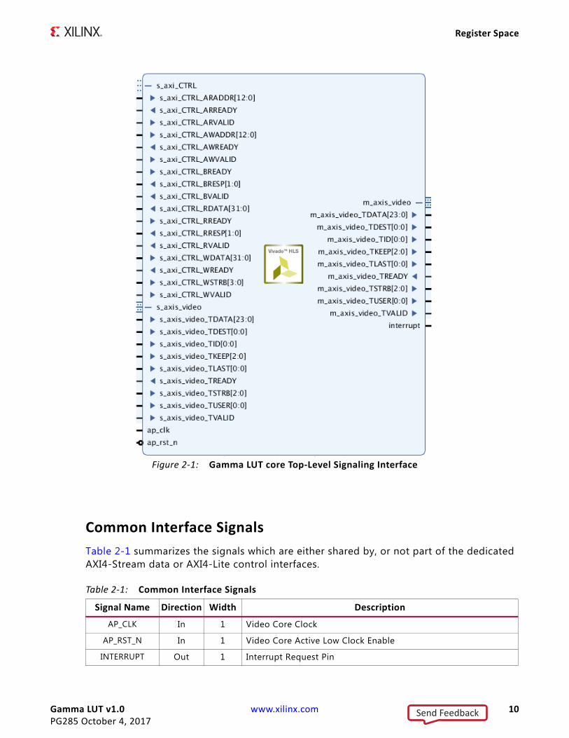
Port Descriptions
The Gamma LUT core uses industry standard control and data interfaces to connect to other system components. The following sections describe the various interfaces available with the core. Figure 2-1 illustrates an I/O diagram of the Gamma LUT core.
Send Feedback
Gamma LUT v1.0 www.xilinx.com 10PG285 October 4, 2017
Register Space
Common Interface Signals
Table 2-1 summarizes the signals which are either shared by, or not part of the dedicated AXI4-Stream data or AXI4-Lite control interfaces.
X-Ref Target - Figure 2-1
Figure 2‐1: Gamma LUT core Top-Level Signaling Interface
Table 2‐1: Common Interface Signals
Signal Name Direction Width Description
AP_CLK In 1 Video Core Clock
AP_RST_N In 1 Video Core Active Low Clock Enable
INTERRUPT Out 1 Interrupt Request Pin
Send Feedback

Gamma LUT v1.0 www.xilinx.com 11PG285 October 4, 2017
Register Space
The AP_CLK and AP_RST_N signals are shared between the core, the AXI4-Stream data interfaces, and the AXI4-Lite control interface. The INTERRUPT pin is not supported and reserved for future use.
AP_CLK
The AXI4-Stream and AXI4-Lite interfaces must be synchronous to the core clock signal AP_CLK. All AXI4-Stream interface input signals and AXI4-Lite control interface input signals are sampled on the rising edge of AP_CLK. All AXI4-Stream output signal changes occur after the rising edge of AP_CLK.
AP_RST_N
The AP_RST_N pin is an active-low, synchronous reset input pertaining to both AXI-Lite and AXI4-Stream interfaces. When AP_RST_N is set to 0, the core resets at the next rising edge of AP_CLK.
Data Interface
The Gamma LUT core receives and transmits data using AXI4-Stream interfaces that implement a video protocol as defined in the Video IP: AXI Feature Adoption section of the (UG761) AXI Reference Guide [Ref 1].
AXI4-Stream Signal Names and Descriptions
Table 2-2 describes the AXI4-Stream signal names and descriptions.
IMPORTANT: In Table 2-2, TotalDataWidth=3*data_width*samples_per_clock. The values correspond to Maximum Data Width and Samples Per Clock in GUI, respectively. Refer to Chapter 4, Design Flow Steps for more information.
Table 2‐2: AXI4-Stream Data Interface Signal Descriptions
Signal Name Direction Width Description
s_axis_video_tdata In (TotalDataWidth+7)/8*8 Input Video Data
s_axis_video_tvalid In 1 Input Video Valid Signal
s_axis_video_tready Out 1 Input Ready
s_axis_video_tuser In 1 Input Video Start Of Frame
s_axis_video_tlast In 1 Input Video End Of Line
s_axi_video_tstrb In s_axis_video tdata/8 Input video data strobe indicates whether the content of the associated byte of TDATA is processed as a data byte or a position byte
Send Feedback

Gamma LUT v1.0 www.xilinx.com 12PG285 October 4, 2017
Register Space
Video Data
The AXI4-Stream interface specification restricts TDATA widths to integer multiples of 8 bits. Therefore, any bit data must be padded with zeros on the MSB to form a N*8 bit wide vector before connecting to s_axis_video_tdata. Padding does not affect the size of the core.
Similarly, data on the Gamma LUT output m_axis_video_tdata is packed and padded to multiples of 8 bits as necessary. Zero padding the most significant bits is only necessary for 10-bit wide data. Figure 2-2 and Figure 2-3 explain the pixel mapping of AXI4-Stream interface with 2 pixels per clock and 10 bits per component configuration for all supporting color formats. Zero padding (bits [63:60]) is not shown in the figures.
s_axi_video_tkeep In s_axis_video tdata/8 Input video byte qualifier that indicates whether the content of the associated byte of TDATA is processed as part of the data stream
s_axi_video_tid In 1 Input video data stream identifier
s_axi_video_tdest In 1 Input video data routing information
m_axis_video_tdata Out (TotalDataWidth+7)/8*8 Output Video Data
m_axis_video_tvalid Out 1 Output Valid
m_axis_video_tready In 1 Output Ready
m_axis_video_tuser Out 1 Output Video Start Of Frame
m_axis_video_tlast Out 1 Output Video End Of Line
m_axi_video_tstrb Out m_axis_video tdata/8
Output video data strobe indicates whether the content of the associated byte of TDATA is processed as a data byte or a position byte
m_axi_video_tkeep Out m_axis_video tdata/8
Output video byte qualifier that indicates whether the content of the associated byte of TDATA is processed as part of the data stream
m_axi_video_tid Out 1 Output video data stream identifier
m_axi_video_tdest Out 1 Output video data routing information
Table 2‐2: AXI4-Stream Data Interface Signal Descriptions (Cont’d)
Signal Name Direction Width Description
Send Feedback

Gamma LUT v1.0 www.xilinx.com 13PG285 October 4, 2017
Register Space
READY/VALID Handshake
A valid transfer occurs whenever READY, VALID, and AP_RST_N are High at the rising edge of AP_CLK, as seen in Figure 2-4. During valid transfers, DATA only carries active video data. Blank periods and ancillary data packets are not transferred through the AXI4-Stream video protocol.
Guidelines on Driving s_axis_video_tvalid
Once s_axis_video_tvalid is asserted, no interface signals (except the Gamma LUT core driving s_axis_video_tready) may change value until the transaction completes (s_axis_video_tready, s_axis_video_tvalid, and AP_RST_N are high on the rising edge of AP_CLK). Once asserted, s_axis_video_tvalid may only be de-asserted after a transaction has completed. Transactions may not be retracted or aborted. In any cycle following a transaction, s_axis_video_tvalid can either be de-asserted or remain asserted to initiate a new transfer.
Guidelines on Driving m_axis_video_tready
The m_axis_video_tready signal may be asserted before, during or after the cycle in which the Gamma LUT core asserted m_axis_video_tvalid. The assertion of
X-Ref Target - Figure 2-2
Figure 2‐2: Dual Pixels per Clock, 10 bits per Component Mapping for RGB
X-Ref Target - Figure 2-3
Figure 2‐3: Dual Pixels per Clock, 10 bits per Component Mapping for YUV 4:4:4
X-Ref Target - Figure 2-4
Figure 2‐4: Example of READY/VALID Handshake, Start of a New Frame
Send Feedback

Gamma LUT v1.0 www.xilinx.com 14PG285 October 4, 2017
Register Space
m_axis_video_tready may be dependent on the value of m_axis_video_tvalid. A slave that can immediately accept data qualified by m_axis_video_tvalid, should pre-assert its m_axis_video_tready signal until data is received. Alternatively, m_axis_video_tready can be registered and driven the cycle following VALID assertion.
RECOMMENDED: To minimize latency, your custom core's slave interface should drive READY independently, or pre-assert READY.
Start of Frame Signals - m_axis_video_tuser0, s_axis_video_tuser0
The Start-Of-Frame (SOF) signal, physically transmitted over the AXI4-Stream TUSER0 signal, marks the first pixel of a video frame. The SOF pulse is 1 valid transaction wide, and must coincide with the first pixel of the frame, as seen in Figure 2-4. The SOF signal serves as a frame synchronization signal, which allows downstream cores to re-initialize, and detect the first pixel of a frame. The SOF signal may be asserted an arbitrary number of AP_CLK cycles before the first pixel value is presented on DATA, as long as a VALID is not asserted.
End of Line Signals - m_axis_video_tlast, s_axis_video_tlast
The End-Of-Line (EOL) signal, physically transmitted over the AXI4-Stream TLAST signal, marks the last pixel of a line. The EOL pulse is 1 valid transaction wide, and must coincide with the last pixel of a scanline, as seen in Figure 2-5.
Control Interface
The AXI4-Lite register interface dynamically controls the behavior of the core. The AXI4-Lite slave interface facilitates integrating the core into a processor system, or along with other video or AXI4-Lite compliant IP, connected through AXI4-Lite interface to an AXI4-Lite master. The core cannot be instantiated without the AXI4-Lite control interface.
X-Ref Target - Figure 2-5
Figure 2‐5: Use of EOL and SOF Signals
Send Feedback

Gamma LUT v1.0 www.xilinx.com 15PG285 October 4, 2017
Register Space
AXI4-Lite Interface
The AXI4-Lite interface allows you to dynamically control parameters within the core. Core configuration can be accomplished using an AXI4-Lite master state machine, or an embedded ARM or soft system processor such as MicroBlaze.
The Gamma LUT core can be controlled through the AXI4-Lite interface by using functions provided by the driver in the SDK. Another method is performing read and write transactions to the Gamma LUT register space but should only be used when the first method is not available.
Table 2‐3: AXI4-Lite Interface Signals
Signal Name Direction Width Description
s_axi_CTRL_awvalid In 1 AXI4-Lite Write Address Channel Write Address Valid.
s_axi_CTRL_awreadOut 1
AXI4-Lite Write Address Channel Write Address Ready. Indicates DMA ready to accept the write address.
s_axi_CTRL_awaddr In 32 AXI4-Lite Write Address Bus
s_axi_CTRL_wvalid In 1 AXI4-Lite Write Data Channel Write Data Valid.
s_axi_CTRL_wready Out 1 AXI4-Lite Write Data Channel Write Data Ready. Indicates DMA is ready to accept the write data.
s_axi_CTRL_wdata In 32 AXI4-Lite Write Data Bus
s_axi_CTRL_bresp Out 2 AXI4-Lite Write Response Channel. Indicates results of the write transfer.
s_axi_CTRL_bvalid Out 1 AXI4-Lite Write Response Channel Response Valid. Indicates response is valid.
s_axi_CTRL_bready In 1 AXI4-Lite Write Response Channel Ready. Indicates target is ready to receive response.
s_axi_CTRL_arvalid In 1 AXI4-Lite Read Address Channel Read Address Valid
s_axi_CTRL_arready Out 1 Ready. Indicates DMA is ready to accept the read address.
s_axi_CTRL_araddr In 32 AXI4-Lite Read Address Bus
s_axi_CTRL_rvalid Out 1 AXI4-Lite Read Data Channel Read Data Valid
s_axi_CTRL_rready In 1 AXI4-Lite Read Data Channel Read Data Ready. Indicates target is ready to accept the read data.
s_axi_CTRL_rdata Out 32 AXI4-Lite Read Data Bus
s_axi_CTRL_rresp Out 2 AXI4-Lite Read Response Channel Response. Indicates results of the read transfer.
Send Feedback

Gamma LUT v1.0 www.xilinx.com 16PG285 October 4, 2017
Register Space
Register Space
The core has 7 core-specific registers which allow you to dynamically control the operation of the core. All registers have initial value of 0. Table 2-4 describes the register names.
Table 2‐4: Register Names and Descriptions
Address (hex)
BASEADDR +Register Name Access
TypeRegister Description
0x0000 Control R/W Bit 0: ap_start (Read/Write/COH)(1)
Bit 1: ap_done (Read/COR)(1)
Bit 2: ap_idle (Read)Bit 3: ap_ready (Read)Bit 7: auto_restart (Read/Write)Others: reserved
0x0004 Global Interrupt Enable R/W Bit 0: Global Interrupt EnableOthers: reservedThis register is not used but reserved for future use.
0x0008 IP Interrupt Enable Register R/W Bit 0: Channel 0 (ap_done)Bit 1: Channel 1 (ap_ready)Others: reservedThis register is not used but reserved for future use.
0x000C IP Interrupt Status Register R Bit 0: Channel 0 (ap_done)Bit 1: Channel 1 (ap_ready)Others: reservedThis register is not used but reserved for future use.
0x0010 Active Width R/W Number of Active Pixels per Scanline
0x0018 Active Height R/W Number of Active Lines per Frame
0x0020 Video Format R/W Specify video color format
0x0fff Gamma look up table 0 R/W Word n: bit [15:0] Gamma LUT 0 [2n] bit [31:16] Gamma LUT 0 [2n+1]
Send Feedback

Gamma LUT v1.0 www.xilinx.com 17PG285 October 4, 2017
Register Space
CONTROL (0x0000) Register
This register controls running of Gamma LUT. Bit 0 of the control register, ap_start, kicks off the core from software. Writing ‘1’ to this bit start the core to generate a video frame. To set the core in free running mode, bit 7 of this register, auto_restart, must be set to ‘1’. Bit 1-3 are not used now but reserved for future use.
ACTIVE_WIDTH (0x0010) Register
The active_width register encodes the number of active pixels per scan. Supported values are 64 and the value provided in the Maximum number of Columns field in the GUI. To avoid processing errors, you should restrict values written to active_width to the range supported by the core instance.
ACTIVE_HEIGHT (0x0018) Register
The active_height register encodes the number of active scan lines per frame. Supported values are between 64 and the value provided in the Maximum number of Rows field in the GUI. To avoid processing errors, you should restrict values written to active_height to the range supported by the core instance.
VIDEO_FORMAT (0x0020) Register
This register specifies the video format of the AXI4-Stream Video data.
• 0x0 RGB video format
• 0x1 YUV 4:4:4 video format
0x17ff Gamma look up table 1 R/W Word n: bit [15:0] Gamma LUT 1 [2n] bit [31:16] Gamma LUT 1 [2n+1]
0x1fff Gamma look up table 2 R/W Word n: bit [15:0] Gamma LUT 2 [2n] bit [31:16] Gamma LUT 2 [2n+1]
Notes: 1. COR = Clear on Read, COH - Clear on Handshake
Table 2‐4: Register Names and Descriptions (Cont’d)
Address (hex)
BASEADDR +Register Name Access
TypeRegister Description
Send Feedback

Gamma LUT v1.0 www.xilinx.com 18PG285 October 4, 2017
Chapter 3
Designing with the Core
General Design GuidelinesThe Gamma LUT core uses look up tables programmed with a gamma correction curve or user-defined function to convert input data to output data.The core processes samples provided via an AXI4-Stream slave interface, outputs pixels via an AXI4-Stream master interface, and can be controlled via the AXI4-Lite interface. The Gamma LUT block cannot change the input/output image sizes, the input and output pixel clock rates, or the frame rate. It is recommended that the Gamma LUT core is used in conjunction with the Xilinx LogiCORE IP Video In to AXI4-Stream and Video Timing Controller cores. The Video Timing Controller core measures the timing parameters, such as number of active scan lines, number of active pixels per scan line of the image sensor. The Video In to AXI4-Stream core converts a clocked parallel video interface with sync and or blank signals to AXI4-Stream.
The core is implemented as a set of LUTs that are used to perform the data transformation. The width of the data determines the number of entries in the LUT. For example, 8-bit data would require 28 (256) entries in the LUT.
Clock, Enable, and Reset Considerations
Clocking
The Gamma LUT IP has a single clock domain. All interfaces (master and slave AXI4-Stream video interfaces and the AXI4-Lite interface) use the ap_clk pin as their clock source.
Resets
The Gamma LUT IP has only a hardware reset option, ap_rst_n pin. No software reset option is available. The external reset pulse must be held for 16 or more ap_clk cycles to reset the core. The ap_rst_n signal is synchronous to the ap_clk clock domain. The ap_rst_n signal resets the entire core including the AXI4-Lite and AXI4-Stream interfaces.
Send Feedback

Gamma LUT v1.0 www.xilinx.com 19PG285 October 4, 2017
Clock, Enable, and Reset Considerations
System Considerations
To operate properly, the Gamma LUT IP must be configured for the actual input and output image frame size. To gather the frame size information from the image video stream, the IP can be connected to the Video In to AXI4-Stream input and the Video Timing Controller core. The timing detector logic in the Video Timing Controller gathers the video timing signals. The AXI4-Lite control interface on the Video Timing Controller allows the system processor to read out the measured frame dimensions and program all downstream cores, such as the Gamma LUT, with the appropriate image dimensions.
Programming Sequence
All Gamma LUT processing parameters other than image size can be changed dynamically on a frame-by-frame basis and the change is picked up immediately. If the image size must be changed or the entire system restarted, it is recommended that pipelined Xilinx® IP video cores are disabled/reset from system output towards the system input, and programmed/enabled from system output to system input.
Send Feedback

Gamma LUT v1.0 www.xilinx.com 20PG285 October 4, 2017
Chapter 4
Design Flow StepsThis chapter describes customizing and generating the core, constraining the core, and the simulation, synthesis and implementation steps that are specific to this IP core. More detailed information about the standard Vivado® design flows and the IP integrator can be found in the following Vivado Design Suite user guides:
• Vivado Design Suite User Guide: Designing IP Subsystems using IP Integrator (UG994) [Ref 7]
• Vivado Design Suite User Guide: Designing with IP (UG896) [Ref 3]
• Vivado Design Suite User Guide: Getting Started (UG910) [Ref 5]
• Vivado Design Suite User Guide: Logic Simulation (UG900) [Ref 6]
Customizing and Generating the CoreThis section includes information about using Xilinx tools to customize and generate the core in the Vivado Design Suite.
If you are customizing and generating the core in the Vivado IP integrator, see the Vivado Design Suite User Guide: Designing IP Subsystems using IP Integrator (UG994) [Ref 7] for detailed information. IP integrator might auto-compute certain configuration values when validating or generating the design. To check whether the values do change, see the description of the parameter in this chapter. To view the parameter value, run the validate_bd_design command in the Tcl console.
You can customize the IP for use in your design by specifying values for the various parameters associated with the IP core using the following steps:
1. Select the IP from the Vivado IP catalog.
2. Double-click the selected IP or select the Customize IP command from the toolbar or right-click menu.
For details, see the Vivado Design Suite User Guide: Designing with IP (UG896) [Ref 3] and the Vivado Design Suite User Guide: Getting Started (UG910) [Ref 5].
Note: Figures in this chapter are illustrations of the Vivado Integrated Design Environment (IDE). The layout depicted here might vary from the current version.
Send Feedback

Gamma LUT v1.0 www.xilinx.com 21PG285 October 4, 2017
Customizing and Generating the Core
Interface
Note: This section provides a quick reference to parameters that can be configured using the Vivado Design Suite at generation time.
The Gamma LUT core is easily configured to meet the user's specific needs through the Vivado Design Suite GUI. This section provides a quick reference to parameters that can be configured at generation time. Figure 4-1 shows the main Vivado Gamma LUT screen.
The main screen displays a representation of the IP symbol on the left side, and the parameter assignments on the right side, which are described as follows:
• Component Name: The component name is used as the base name of output files generated for the module. Names must begin with a letter and must be composed from characters: a to z, 0 to 9 and “_”. The name v_gamma_lut_v1_0 is not allowed.
• Samples Per Clock: Specifies the number of pixel processed per clock cycle. Permitted values are 1, 2, 4, and 8 samples per clock. This parameter determines IP's throughput. The more samples per clock, the larger throughput it provides. The larger throughput always needs more hardware resources.
• Maximum Data Width: Specifies the bit width of input samples. Permitted values are 8, 10, 12 and 16 bits. This parameter should match the Video Component Width of the video IP core connected to the slave AXI-Stream video interface.
• Maximum Number of Columns: Specifies maximum video columns/pixels the IP core could produce at runtime. Any video width that is less than Maximum Number of Columns can be programmed through AXI4-Lite control interface without regenerating core.
• Maximum Number of Rows: Specifies maximum video rows/lines the IP core could produce at runtime. Any video height that is less than Maximum Number of Rows can be programmed through AXI4-Lite control interface without regenerating core.
X-Ref Target - Figure 4-1
Figure 4‐1: Gamma LUT Vivado IP Catalog GUI
Send Feedback

Gamma LUT v1.0 www.xilinx.com 22PG285 October 4, 2017
Output Generation
User Parameters
Table 4-1 shows the relationship between the fields in the Vivado IDE and the User Parameters (which can be viewed in the Tcl Console).
Output GenerationFor details, see “Generating IP Output Products” in the Vivado Design Suite User Guide: Designing with IP (UG896) [Ref 3].
Constraining the CoreThis section contains information about constraining the core in the Vivado Design Suite.
Required Constraints
The only constraints required are clock frequency constraints for the core clock, ap_clk. Paths from AXI4-Lite signals should be constrained with a set_false_path, causing setup and hold checks to be ignored for AXI4-Lite signals. These constraints are provided in the XDC constraints file included with the core.
Device, Package, and Speed Grade Selections
This section is not applicable for this IP core.
Clock Frequencies
This section is not applicable for this IP core.
Table 4‐1: Vivado IDE Parameter to User Parameter Relationship
Vivado IDE Parameter/Value User Parameter/Value Default Value
Top-Level Parameters
Samples per Clock SAMPLES_PER_CLOCK 1
Maximum Number of Columns MAX_COLS 3840
Maximum Number of Rows MAX_ROWS 2160
Maximum Data Width MAX_DATA_WIDTH 8
Send Feedback

Gamma LUT v1.0 www.xilinx.com 23PG285 October 4, 2017
Simulation
Clock Management
This section is not applicable for this IP core.
Clock Placement
This section is not applicable for this IP core.
Banking
This section is not applicable for this IP core.
Transceiver Placement
This section is not applicable for this IP core.
I/O Standard and Placement
This section is not applicable for this IP core.
SimulationFor comprehensive information about Vivado simulation components, as well as information about using supported third party tools, see the Vivado Design Suite User Guide: Logic Simulation (UG900) [Ref 6].
Synthesis and ImplementationThis section contains information about synthesis and implementation in the Vivado Design Suite. For details about synthesis and implementation, see “Synthesizing IP” and “Implementing IP” in the Vivado Design Suite User Guide: Designing with IP (UG896) [Ref 3].
Send Feedback

Gamma LUT v1.0 www.xilinx.com 24PG285 October 4, 2017
Chapter 5
Detailed Example DesignThis chapter provides two example systems that include the Gamma LUT core. One is simulation example design and the other one is synthesizable example design. Important system-level aspects when designing with the Gamma LUT are highlighted in example designs, including:
• Typical usage of Gamma LUT in conjunction with other cores and AXI master.
• Configuration of Gamma LUT registers on the fly.
Note: The example project is only available on Xilinx KC705 evaluation board.
To open the example project, perform following:
1. Select the Gamma LUT IP from IP Catalog.
2. Double-click on the selected IP or right-click the IP and select Customize IP from the menu.
3. Configure the build-time parameters in the Customize IP window and click OK. The Vivado IDE generates an example design matching the build-time configuration.
4. In the Generate Output Products window, select Generate or Skip. If Generate is selected, the IP’s output products are generated after a brief moment.
5. Right-click Gamma LUT in Sources panel and select Open IP Example Design from the menu.
6. In the Open IP Example Design window, select example project directory and click OK. The Vivado software then runs automation to generate example design in selected directory.
The generated project contains two example designs. Figure 5-1 shows the Source panel of the example project. Synthesizable example block design, along with top-level file, resides in Design Sources catalog. Simulation example design files (including block design file and SystemVerilog test bench) are under Simulation Sources.
Send Feedback

Gamma LUT v1.0 www.xilinx.com 25PG285 October 4, 2017
Simulation Example Design
Simulation Example DesignThe simulation example design contains the following video IP cores:
• Video Test Pattern Generator (TPG)
• Gamma LUT
• Video Timing Controller (VTC)
• AXI4-Stream to Video Output bridge
The design also contains a AXI Verification IP (VIP) core (to enable register programming) connected to an AXI interconnect.
After all configurations are performed, the AXI VIP core starts the TPG, Gamma LUT, and Video Timing Controller cores. Because this design runs an RTL simulation, running large video frames can take a long time. Xilinx® recommends running a small video size for this example design. Width and height values, as well as other register settings, can be changed in the simulation test bench v_gamma_lut_0_exdes_tb.sv file.
The v_tpg_0 core is in free-running mode after kickoff. It generates video stream pixels at clock rate of ap_clk.
The v_gamma_lut_0 core receives video frames from AXI-Stream Slave interface and generates video output.
AXI4-Stream to Video Out core, working with Video Timing Controller, interfaces from the AXI4-Stream interface implementing a Video Protocol to a video source (parallel video data, video syncs, and blanks).
X-Ref Target - Figure 5-1
Figure 5‐1: Example Project Source Panel
Send Feedback

Gamma LUT v1.0 www.xilinx.com 26PG285 October 4, 2017
Simulation Example Design
The example design checks the output port locked from the AXI4-Stream to Video Out core. The locked port indicates that the output timing is locked to the output video. The example design indicates that the test completed successfully if video lock is successfully detected.
Send Feedback

Gamma LUT v1.0 www.xilinx.com 27PG285 October 4, 2017
Simulation Example Design
X-Ref Target - Figure 5-2
Figure 5‐2: Simulation Example Block Design
Send Feedback

Gamma LUT v1.0 www.xilinx.com 28PG285 October 4, 2017
Synthesizable Example Design
Synthesizable Example DesignThe difference between the Synthesizable design and the Simulation example design is the use of the MicroBlaze microprocessor instead of the AXI VIP core as AXI master. The locked port of AXI4-Stream to Video Out is connected to axi_gpio_lock core and MicroBlaze polls the corresponding register for a sign that the test passed.
Send Feedback

Gamma LUT v1.0 www.xilinx.com 29PG285 October 4, 2017
Synthesizable Example Design
X-Ref Target - Figure 5-3
Figure 5‐3: Synthesizable Example Block Design
Send Feedback
Gamma LUT v1.0 www.xilinx.com 30PG285 October 4, 2017
Synthesizable Example Design
The synthsizable example design requires both Vivado and Xilinx SDK tools.
The first step is to run synthesis, implementation and bitstream generation in Vivado. After all those steps are done, select File -> Export -> Export Hardware. In the window, select Include bitstream, select an export directory and click OK.
The remaining work is performed in Xilinx SDK tool. The Gamma LUT example design file can be found at SDK directory:
(<install_directory>/<release>/data/embeddedsw/XilinxProcessorIPLib/drivers/v_gamma_lut_v1_0/examples/
Example application design source files (contained within "examples" folder) are tightly coupled with the Gamma LUT example design available in Vivado Catalog.
vgamma_lut_example.tcl automates the process of generating the downloadable bit and elf files from the provided example hdf file.
To run the provided Tcl script:
1. Copy the exported example design hdf file in the "examples" directory of the driver
2. Launch the Xilinx Software Command-Line Tool (xsct) terminal
3. cd into the examples directory
4. Source the tcl file
xsct%>source vgamma_lut_example.tcl
5. Execute the script
xsct%>vgamma_lut_example <hdf_file_name.hdf>
The Tcl script cript performs the following:
• Create workspace
• Create HW project
• Create BSP
• Create Application Project
• Build BSP and Application Project
After the process is complete, the required files are available in:
bit file -> vgamma_lut_example.sdk/vgamma_lut_example_hw_platform folderelf file -> vgamma_lut_example.sdk/vgamma_lut_example_design/{Debug/Release} folder
Next, perform the following steps to run the software application:
Send Feedback

Gamma LUT v1.0 www.xilinx.com 31PG285 October 4, 2017
Synthesizable Example Design
IMPORTANT: To do so, make sure that the hardware is powered on and a Digilent Cable or an USB Platform Cable is connected to the host PC. Also, ensure that a USB cable is connected to the UART port of the KC705 board.
1. Launch SDK.
2. Set workspace to vgamma_lut_example.sdk folder in prompted window. The SDK project opens automatically. (If a welcome page shows up, close that page.)
3. Download the bitstream into the FPGA by selecting Xilinx Tools > Program FPGA. The Program FPGA dialog box opens.
4. Ensure that the Bitstream field shows the bitstream file generated by Tcl script, and then click Program.
Note: The DONE LED on the board turns green if the programming is successful.
5. A terminal program (HyperTerminal or PuTTY) is needed for UART communication. Open the program, choose appropriate port, set baud rate to 115200 and establish Serial port connection.
6. Select and right-click the application vgamma_lut_example_design in Project_Explorer panel.
7. Select Run As > Launch on Hardware (System Debugger).
8. Select Binaries and Qualifier in window and click OK.
The example design test result are shown in terminal program.
For more information, visit www.xilinx.com/tools/sdk.htm.
When executed on the board, the example application performs following:
• Program Video Clock Generator to 1080p@60Hz
• Program TPG and Gamma LUT to 1080p@60Hz
• Check for Video Lock and report the status (PASS/FAIL) on UART
• Repeat Steps 1-3 for 4KP@30Hz and 4KP@60Hz
Send Feedback

Gamma LUT v1.0 www.xilinx.com 32PG285 October 4, 2017
Chapter 6
Test BenchNo test bench is available at this time. For a comprehensive listing of Video and Imaging application notes, white papers, related IP cores including the most recent reference designs available, see the Video and Imaging Resources page at www.xilinx.com/esp/video/refdes_listing.htm.
Send Feedback

Gamma LUT v1.0 www.xilinx.com 33PG285 October 4, 2017
Appendix A
Verification, Compliance, and Interoperability
SimulationA highly parameterizable test bench was used to test the Gamma LUT core in Vivado® HLS. Testing included the following:
• Register accesses
• Processing multiple frames of data
• Varying IP throughput and pixel data width
• Testing of various frame sizes
• Varying parameter settings
Hardware TestingThe Gamma LUT core has been validated in hardware at Xilinx® to represent a variety of parameterizations, including the following:
• A test design was developed for the core that incorporated a MicroBlaze™ processor, AXI4-Lite interconnect and various other peripherals. The MicroBlaze processor was responsible for:
° Programing the video clock to match tested video resolution
° Configuring the Gamma LUT core with different resolutions
° Launching the test
° Reporting the Pass/Fail status of the test and any errors that were found
Send Feedback

Gamma LUT v1.0 www.xilinx.com 34PG285 October 4, 2017
Interoperability
InteroperabilityThe core slave (input) AXI4-Stream interface can work directly with any core that produces RGB or YUV 444 video data.
Send Feedback

Gamma LUT v1.0 www.xilinx.com 35PG285 October 4, 2017
Appendix B
UpgradingThis appendix contains information about upgrading to a more recent version of the IP core.
This appendix does not apply to this core.
Send Feedback

Gamma LUT v1.0 www.xilinx.com 36PG285 October 4, 2017
Appendix C
DebuggingThis appendix includes details about resources available on the Xilinx Support website and debugging tools.
Finding Help on Xilinx.comTo help in the design and debug process when using the Gamma LUT, the Xilinx Support web page (Xilinx Support web page) contains key resources such as product documentation, release notes, answer records, information about known issues, and links for opening a Technical Support Web Case.
Documentation
This product guide is the main document associated with the Gamma LUT. This guide, along with documentation related to all products that aid in the design process, can be found on the Xilinx Support web page or by using the Xilinx Documentation Navigator.
Download the Xilinx Documentation Navigator from the Downloads page. For more information about this tool and the features available, open the online help after installation.
Answer Records
Answer Records include information about commonly encountered problems, helpful information on how to resolve these problems, and any known issues with a Xilinx product. Answer Records are created and maintained daily ensuring that users have access to the most accurate information available.
Answer Records for this core are listed below, and can also be located by using the Search Support box on the main Xilinx support web page. To maximize your search results, use proper keywords such as
• Product name
• Tool message(s)
• Summary of the issue encountered
Send Feedback

Gamma LUT v1.0 www.xilinx.com 37PG285 October 4, 2017
Appendix C: Debugging
A filter search is available after results are returned to further target the results.
Answer Records for the Gamma LUT Core
AR 68768
Technical Support
Xilinx provides technical support in the Xilinx Support web page for this LogiCORE™ IP product when used as described in the product documentation. Xilinx cannot guarantee timing, functionality, or support if you do any of the following:
• Implement the solution in devices that are not defined in the documentation.
• Customize the solution beyond that allowed in the product documentation.
• Change any section of the design labeled DO NOT MODIFY.
Xilinx provides premier technical support for customers encountering issues that require additional assistance.
To contact Xilinx Technical Support, navigate to the Xilinx Support web page.
1. Open a WebCase by selecting the WebCase link located under Support Quick Links.
• A block diagram of the video system that explains the video source, destination and IP (custom and Xilinx) used.
Note: Access to WebCase is not available in all cases. Please login to the WebCase tool to see your specific support options.
Debug ToolsThere are many tools available to address Gamma LUT core design issues. It is important to know which tools are useful for debugging various situations.
Vivado Design Suite Debug Feature
Vivado® lab tools insert logic analyzer and virtual I/O cores directly into your design. Vivado lab tools allows you to set trigger conditions to capture application and integrated block port signals in hardware. Captured signals can then be analyzed. This feature represents the functionality in the Vivado IDE that is used for logic debugging and validation of a design running in Xilinx devices in hardware.
The Vivado lab tools logic analyzer is used to interact with the logic debug LogiCORE IP cores, including:
Send Feedback

Gamma LUT v1.0 www.xilinx.com 38PG285 October 4, 2017
Appendix C: Debugging
• ILA 2.0 (and later versions)
• VIO 2.0 (and later versions)
See Vivado Design Suite User Guide: Programming and Debugging (UG908).
Hardware DebugHardware issues can range from link bring-up to problems seen after hours of testing. This section provides debug steps for common issues. The Vivado lab tools are a valuable resource to use in hardware debug. The signal names mentioned in the following individual sections can be probed using the Vivado lab tools for debugging the specific problems.
General Checks
Ensure that all the timing constraints for the core were properly incorporated from the example design and that all constraints were met during implementation.
• Does it work in post-place and route timing simulation? If problems are seen in hardware but not in timing simulation, this could indicate a PCB issue. Ensure that all clock sources are active and clean.
• If using MMCMs in the design, ensure that all MMCMs have obtained lock by monitoring the LOCKED port.
Send Feedback

Gamma LUT v1.0 www.xilinx.com 39PG285 October 4, 2017
Appendix D
Additional Resources
Xilinx ResourcesFor support resources such as Answers, Documentation, Downloads, and Forums, see Xilinx Support.
Documentation Navigator and Design HubsXilinx® Documentation Navigator provides access to Xilinx documents, videos, and support resources, which you can filter and search to find information. To open the Xilinx Documentation Navigator (DocNav):
• From the Vivado® IDE, select Help > Documentation and Tutorials.
• On Windows, select Start > All Programs > Xilinx Design Tools > DocNav.
• At the Linux command prompt, enter docnav.
Xilinx Design Hubs provide links to documentation organized by design tasks and other topics, which you can use to learn key concepts and address frequently asked questions. To access the Design Hubs:
• In the Xilinx Documentation Navigator, click the Design Hubs View tab.
• On the Xilinx website, see the Design Hubs page.
Note: For more information on Documentation Navigator, see the Documentation Navigator page on the Xilinx website.
Send Feedback

Gamma LUT v1.0 www.xilinx.com 40PG285 October 4, 2017
References
ReferencesThese documents provide supplemental material useful with this user guide:
1. Vivado AXI Reference Guide (UG1037)
2. ISE to Vivado Design Suite Migration Guide (UG911)
3. Vivado Design Suite User Guide: Designing with IP (UG896)
4. Vivado Design Suite User Guide: Programming and Debugging (UG908)
5. Vivado Design Suite User Guide: Getting Started (UG910)
6. Vivado Design Suite User Guide: Logic Simulation (UG900)
7. Vivado Design Suite User Guide: Designing IP Subsystems using IP Integrator (UG994)
Revision HistoryThe following table shows the revision history for this document.
Date Version Revision
10/04/2017 1.0 Initial Release
Send Feedback

Gamma LUT v1.0 www.xilinx.com 41PG285 October 4, 2017
Notice of Disclaimer
Notice of DisclaimerThe information disclosed to you hereunder (the “Materials”) is provided solely for the selection and use of Xilinx products. To the maximum extent permitted by applicable law: (1) Materials are made available "AS IS" and with all faults, Xilinx hereby DISCLAIMS ALL WARRANTIES AND CONDITIONS, EXPRESS, IMPLIED, OR STATUTORY, INCLUDING BUT NOT LIMITED TO WARRANTIES OF MERCHANTABILITY, NON-INFRINGEMENT, OR FITNESS FOR ANY PARTICULAR PURPOSE; and (2) Xilinx shall not be liable (whether in contract or tort, including negligence, or under any other theory of liability) for any loss or damage of any kind or nature related to, arising under, or in connection with, the Materials (including your use of the Materials), including for any direct, indirect, special, incidental, or consequential loss or damage (including loss of data, profits, goodwill, or any type of loss or damage suffered as a result of any action brought by a third party) even if such damage or loss was reasonably foreseeable or Xilinx had been advised of the possibility of the same. Xilinx assumes no obligation to correct any errors contained in the Materials or to notify you of updates to the Materials or to product specifications. You may not reproduce, modify, distribute, or publicly display the Materials without prior written consent. Certain products are subject to the terms and conditions of Xilinx’s limited warranty, please refer to Xilinx’s Terms of Sale which can be viewed at https://www.xilinx.com/legal.htm#tos; IP cores may be subject to warranty and support terms contained in a license issued to you by Xilinx. Xilinx products are not designed or intended to be fail-safe or for use in any application requiring fail-safe performance; you assume sole risk and liability for use of Xilinx products in such critical applications, please refer to Xilinx’s Terms of Sale which can be viewed at https://www.xilinx.com/legal.htm#tos.AUTOMOTIVE APPLICATIONS DISCLAIMERAUTOMOTIVE PRODUCTS (IDENTIFIED AS "XA" IN THE PART NUMBER) ARE NOT WARRANTED FOR USE IN THE DEPLOYMENT OF AIRBAGS OR FOR USE IN APPLICATIONS THAT AFFECT CONTROL OF A VEHICLE ("SAFETY APPLICATION") UNLESS THERE IS A SAFETY CONCEPT OR REDUNDANCY FEATURE CONSISTENT WITH THE ISO 26262 AUTOMOTIVE SAFETY STANDARD ("SAFETY DESIGN"). CUSTOMER SHALL, PRIOR TO USING OR DISTRIBUTING ANY SYSTEMS THAT INCORPORATE PRODUCTS, THOROUGHLY TEST SUCH SYSTEMS FOR SAFETY PURPOSES. USE OF PRODUCTS IN A SAFETY APPLICATION WITHOUT A SAFETY DESIGN IS FULLY AT THE RISK OF CUSTOMER, SUBJECT ONLY TO APPLICABLE LAWS AND REGULATIONS GOVERNING LIMITATIONS ON PRODUCT LIABILITY.This document contains preliminary information and is subject to change without notice. Information provided herein relates to products and/or services not yet available for sale, and provided solely for information purposes and are not intended, or to be construed, as an offer for sale or an attempted commercialization of the products and/or services referred to herein.© Copyright 2017 Xilinx, Inc. Xilinx, the Xilinx logo, Artix, ISE, Kintex, Spartan, Virtex, Vivado, Zynq, and other designated brands included herein are trademarks of Xilinx in the United States and other countries. All other trademarks are the property of their respective owners.
Send Feedback