Embed Size (px)
Citation preview

499
Gallium Arsen23. Gallium Arsenide
The history of gallium arsenide is complicatedbecause the technology required to produce GaAsdevices has been fraught with problems associatedwith the material itself and with difficulties inits fabrication. Thus, for many years, GaAs waslabelled as “the semiconductor of the future, andit will always be that way.” Recently, however,advances in compact-disc (CD) technology, fibre-optic communications and mobile telephonyhave boosted investment in GaAs research anddevelopment. Consequently, there have beenadvances in materials and fabrication technologyand, as a result, GaAs devices now enjoy stableniche markets.
The specialised uses for GaAs in high-frequencyand optoelectronic applications result from thephysical processes of electron motion that allowhigh-speed and efficient light emission to takeplace. In this review, these advanced devices areshown to result from the physical properties ofGaAs as a semiconducting material, the controlledgrowth of GaAs and its alloys and the subsequentfabrication into devices.
Extensive use is made of chapters from“Properties of Gallium Arsenide, 3rd edition” whichI edited with the help of Prof. G. E. Stillman [23.1].This book was written to reflect virtually all aspectsof GaAs and its devices within a readable text.I believe that we succeeded in that aim and Imake no apologies in referring to it. Readerswho need specialised data, but not necessarilywithin an explanatory text, should refer to theLandolt-Bornstein, group III (condensed matter)data collection [23.2, 3]. The sub-volumes A1α(lattice properties) and A2α (impurities anddefects) within volume 41 are rich sources of datafor all III–V compounds. Although there are nobetter sources than the original research papers,I have referred to textbooks where possible. Thisis because the presentation and discussion ofscientific data is often clearer than in the originaltext, and these books are more accessible tostudents.
Gallium arsenide (GaAs) is one of the mostuseful of the III–V semiconductors. In this chapter,the properties of GaAs are described and theways in which these are exploited in devices areexplained. The limitations of this material arepresented in terms of both its physical and itselectronic properties.
23.1 Bulk Growth of GaAs ............................ 50223.1.1 Doping Considerations ............... 50223.1.2 Horizontal Bridgman
and Horizontal Gradient FreezeTechniques ............................... 503
23.1.3 Liquid-Encapsulated Czochralski(LEC) Technique ......................... 504
23.1.4 Vertical Gradient Freeze (VGF)Technique ................................ 506
23.2 Epitaxial Growth of GaAs ...................... 50723.2.1 Liquid-Phase Epitaxy (LPE) ......... 50723.2.2 Vapour-Phase Epitaxy (VPE)
Technologies ............................ 50823.2.3 Molecular-Beam Epitaxy (MBE) ... 50923.2.4 Growth of Epitaxial
and Pseudomorphic Structures ... 511
23.3 Diffusion in Gallium Arsenide ............... 51123.3.1 Shallow Acceptors ..................... 51223.3.2 Shallow Donors ......................... 51323.3.3 Transition Metals....................... 513
23.4 Ion Implantation into GaAs .................. 513
23.5 Crystalline Defects in GaAs .................... 51423.5.1 Defects in Melt-Grown GaAs ....... 51423.5.2 Epitaxial GaAs (not Low
Temperature MBE GaAs) ............. 51623.5.3 LTMBE GaAs .............................. 517
23.6 Impurity and Defect Analysisof GaAs (Chemical) ............................... 517
23.7 Impurity and Defect Analysisof GaAs (Electrical) ............................... 51823.7.1 Introduction to Electrical Analysis
of Defects in GaAs ..................... 518
23.8 Impurity and Defect Analysisof GaAs (Optical) .................................. 52123.8.1 Optical Analysis of Defects in GaAs 521
PartC
23

500 Part C Materials for Electronics
23.9 Assessmentof Complex Heterostructures ................. 52223.9.1 Carrier Concentration
Measurementsin Heterostructures.................... 522
23.9.2 Layer Thickness and CompositionMeasurements .......................... 522
23.10 Electrical Contacts to GaAs .................... 52423.10.1 Ohmic Contacts ......................... 52423.10.2 Schottky Contacts ...................... 524
23.11 Devices Based on GaAs (Microwave) ....... 52423.11.1 The Gunn Diode ........................ 52423.11.2 The Metal–Semiconductor
Field-Effect Transistor (MESFET) ... 525
23.11.3 The High-Electron-MobilityTransistor (HEMT)or Modulation Doped FET(MODFET) .................................. 526
23.11.4 The Heterojunction BipolarTransistor (HBT) ......................... 526
23.12 Devices based on GaAs (Electro-optical) . 52723.12.1 GaAs Emitters ........................... 52723.12.2 GaAs Modulators ....................... 53123.12.3 GaAs Photodetectors .................. 531
23.13 Other Uses for GaAs.............................. 532
23.14 Conclusions ......................................... 532
References .................................................. 533
GaAs is one of the compound semiconductors that occurin the zincblende structure. As can be seen in Fig. 23.1,each Ga atom is tetrahedrally bonded to four As atomsin a structure that is similar to the diamond lattice butwith alternating Ga and As atoms.
The presence of two types of atoms introducesa small component of ionic bonding into the struc-ture and increases the bond strength above thatof the group IV element (Ge) which Ga and Asneighbour. As a result the band-gap energy Eg, is in-creased to 1.518 eV at T = 0 K (Eg = 1.41 eV at roomtemperature).
The lattice constant of GaAs at 300 K is 0.565 36 nm,giving a resultant density of 5.3165 g/cm3. At atmo-spheric pressure GaAs melts near 1238 C but with theloss of As vapour.
a
Ga
As
Fig. 23.1 The zincblende lattice of GaAs. The lattice con-stant a is indicated. (After [23.4])
Although all 〈001〉 atomic planes are equivalent thisis not true for 〈011〉 and 〈111〉 planes. In particular,there are two types of 〈111〉 atomic planes; one ter-minated with Ga atoms only (the 〈111〉A planes), theother being terminated with As atoms only (the 〈111〉Bplanes). This makes the 〈111〉 directions strongly polar.A further consequence of the reduced symmetry of thelattice compared with the group IV semiconductors isthat GaAs exhibits strong piezoelectric effects.
The easily cleaved directions are the 〈110〉 and 〈111〉types. The 〈110〉 are the more useful as they allow squaresections to be cleaved from a 〈001〉 section wafer, oneof the major reasons for the use of 〈001〉 wafers in GaAsdevice fabrication.
The original interest in GaAs arose from its unusualband structure, compared to that of Si in Fig. 23.2, whichdemonstrates several attributes that are expected to be in-teresting for high-speed electronics and optoelectronics.
1. The fundamental band-gap energy of 1.41 eV(300 K) corresponds to a point in the diagram, the Γ
point of the Brillouin zone, where both the crystalmomentum for holes and electrons is zero. It followsthat low-energy electrons and holes can recombinewithout the moderating influence of phonons thatwould otherwise be required to conserve momen-tum. Such direct recombination is expected to resultin efficient emission of photons and GaAs wouldthen be the base material for efficient light-emittingdiodes (LEDs) and lasers.
2. The effective mass of conduction-band electrons isinversely proportional to the curvature at the bottomof the band and this curvature is considerably greater,and the effective mass is considerably smaller, inGaAs (about 0.063 me) than in silicon (about 1.1 me).
PartC
23

Gallium Arsenide 501
Table 23.1 Selected important properties of pure GaAs at300 K
Lattice constant (Å) 5.653
Density (g/cm3) 5.318
Band-gap energy (eV) 1.424
Band-gap type Direct
Electron mobility (cm2/Vs) 8500
Hole mobility (cm2/Vs) 400
Zero-frequency dielectric constant 13.18
Conduction-band effective density 4.45 × 10¹⁷
of states (cm−3)
Valence-band effective density 7.72 × 10¹⁸
of states (cm−3)
Intrinsic carrier concentration (cm−3) 1.84 × 10⁶
Because the mobility of carriers is inversely propor-tional to their effective mass, it follows that freeelectrons in GaAs should be very mobile underthe influence of an electric field, resulting in fastdevices.
3. An additional feature of Fig. 23.2 is the occurrenceof subsidiary conduction-band minima near the sixpoints of maximum momentum along the 〈100〉 di-rections. These are at the so-called L points of theBrillouin zone. These minima are degenerate and atan energy of 0.3 eV above the minimum energy ofthe conduction band at the Γ point. The relativelysmall curvature of these X minima results in a largeeffective electron mass of about 1.2 me. Electrons atthese points have a correspondingly low mobility.It follows that the excitation of low-effective-massfree electrons from the Γ point to the L minima,where they have high effective mass, can result ina reduction of electron velocity and hence elec-tron current. This is the transferred electron effect.The current/voltage characteristics of such a de-vice exhibit a negative differential resistance region,the Gunn effect, and this can be used to generatemicrowave radiation.
4. One property of GaAs, not resulting from Fig. 23.2,is that the material can be produced in a highelectrical resistivity, semi-insulating (SI) state. Thisallows devices to be fabricated on a near-insulatingsubstrate. This is advantageous for high-frequencydevices as the parasitic capacitances that occur be-tween Si devices and their substrate, reducing their
Energy (eV)
Crystal momentum p–0
4
3
2
1
0
–1
–20[111] [100] [111] [100]p– c
a) b)
Si Conductionband
GaAs Conductionband
Valenceband
Valenceband
Eg
∆E = 0.31
Eg
Fig. 23.2a,b The band structures of (a) Si and (b) GaAs. The pri-mary band gap of Si is indirect with an energy Eg, of 1.12 eV.However, that of GaAs is direct (both free electrons and holes oflow energy have states that correspond to zero crystal momentumat the Γ point of the Brillouin zone). Secondary conduction-bandminima occur at 0.31 eV above the primary minimum near points ofmaximum crystal momenta along the [111]-directions. These are atthe L points. (After [23.4])
maximum operating frequency, will be absent inGaAs devices fabricated on SI substrates.
5. A further property of great interest is that the latticeconstants of GaAs and aluminium arsenide, AlAs,and their alloys, written as Ga1−xAlxAs, where xis the atomic fraction of Al, are very similar. Thisallows different alloys to be grown consecutivelywithout incurring defects due to lattice mismatch.Such heterostructures are not possible with Si andits known alloys.
The predictions made above will be addressed inlater sections but first we consider the growth of GaAssingle crystals suitable for device use. Subsequently, weconsider the epitaxial growth of thin, GaAs-based layers,which are the basis of modern devices, means of pro-cessing and the fabrication and properties of importantdevices.
PartC
23

502 Part C Materials for Electronics
23.1 Bulk Growth of GaAs
In the simplest terms, GaAs crystals are synthesisedby reacting together high-purity Ga and As. Dopantsmay be added to produce materials of different conduc-tion type and carrier concentration. However, the growthof compounds from the melt is a thermodynamic pro-cess and is characterised by the shape of the phasediagram near the solidus at temperatures just belowthe melting point of the compound. Hurle has pub-lished a thorough reassessment of the thermodynamicparameters for GaAs, with and without doping [23.6].The complete phase diagram for Ga−As, showing theGaAs compound, is shown in Fig. 23.3. However, de-tails near the GaAs solidus are not revealed at this largescale.
The shape of the GaAs solidus is more complicatedthan indicated in Fig. 23.3. In particular, the congruentpoint, the maximum melting temperature, correspondsto a GaAs compound containing more As than exists instoichiometric material (Fig. 23.4).
Temperature (°C)
Atomic percent of arsenic0 100
1400
1200
1000
800
600
400
200
20 40 60 80Ga
GaAs + Ga
GaAs + Ga
Solution + GaAs
Solution + GaAs
As
1238°
Fig. 23.3 The complete phase diagram of the Ga−As sys-tem at an assumed pressure of As vapour of about 1 atm.The vertical line near 50% composition is crystalline GaAs.(After [23.5])
It follows that growth from a stoichiometric meltresults in the growth of a solid phase containing an ex-cess of As of approximately 1 × 1019 cm−3. The solidusis retrograde so that, if thermodynamic equilibrium ismaintained, this excess As must be lost from the host asthe solid cools. If this As supersaturation cannot be re-lieved by out-diffusion from the crystal, then it will resultin the generation of As-rich second phases (precipitates).Growth from a Ga-rich melt will result in the growth ofa stoichiometric crystal. However, the melt will becomemore Ga-rich as growth proceeds, leading to the growthof solid GaAs that steadily becomes richer in Ga.
Experimental work has shown that the electricalproperties of Ga-rich GaAs are poor (undoped Ga-richGaAs is strongly p-type [23.7]) and this growth regimeis rarely used. Although As richness is found in melt-grown GaAs, measured concentrations of excess As donot exceed 1017 cm−3 [23.8,9]. It is not known how mostof the grown-in excess As atoms are lost.
23.1.1 Doping Considerations
Unlike group IV semiconductors where shallow donorsare group V atoms only, donors in III–V compounds canoccur on either sublattice, as IVIII or VIV, where the
T (K)
δ1.5 × 10¹⁹
1600
–1.5
1400
1200
1000
800
600
500–1 –0.5 0.5 10
Fig. 23.4 The GaAs solidus. The arrow marks the congru-ent point (After [23.6])
PartC
23.1
Gallium Arsenide 23.1 Bulk Growth of GaAs 503
capital letters represent the group in the periodic tablefrom which the donor is selected and the subscript isthe sublattice occupied. However, only certain group IVatoms have a suitable solubility on the Ga sublatticefor them to be useful and the same situation is true forgroup VI atoms on As sites.
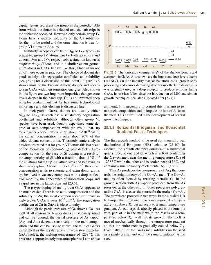
Similarly, acceptors can be of IIIII or IVV types. (Inprinciple, group IV atoms can be both acceptors anddonors, IVIII and IVV respectively, a situation known asamphotericity. Silicon, and to a similar extent germa-nium atoms in GaAs, behave like this.) Once again notall of these occur in practice. The choice of dopant de-pends mainly on its segregation coefficient and solubility(see [23.6] for a discussion of this point). Figure 23.5shows most of the known shallow donors and accep-tors in GaAs with their ionisation energies. Also shownin this figure are two important impurities that generatelevels deeper in the band gap. Cu is an unwanted deepacceptor contaminant but Cr has some technologicalimportance and this element is discussed later.
In melt-grown GaAs, donors are usually eitherSiGa or TeAs, as each has a satisfactory segregationcoefficient and solubility, although other group VIspecies have been used. Donors experience some de-gree of auto-compensation with the result that, upto a carrier concentration n of about 3 × 1018 cm−3,the carrier concentration is only about 80% of theadded dopant concentration. Thermodynamic analysishas demonstrated that for group VI donors this is a resultof the formation of (donor–VGa) pair defects. Auto-compensation for the case of Si doping is a result ofthe amphotericity of Si with a fraction, about 10%, ofthe Si atoms taking up As lattice sites and behaving asshallow acceptors. Above n = 3 × 1018 cm−3, the carrierconcentration tends to saturate and extra donor atomsare involved in vacancy complexes with a drop in elec-tron mobility, the appearance of dislocation loops anda rapid rise in the lattice constant [23.6].
The p-type doping of melt-grown GaAs appears tobe much easier. There is no auto-compensation and thesolubility of Zn, the most common acceptor dopant inmelt-grown GaAs, is over 1020 cm−3. The segregationcoefficient of Zn in GaAs is close to unity.
Although the partial pressure of Ga above a Ga−Asmelt at all reasonable temperatures is extremely smalland can be ignored, the partial pressure of As vapour(As2 and As4) depends sensitively on the melt compo-sition and this can be used to control the ratio of Ga/Asin the melt as the crystal grows. Over a stoichiometricGaAs melt at the melting temperature of 1238 C thispressure is approximately two atmospheres (1 atm above
0.006
S
1.42
0.006
Se
0.006
Sn
0.03
Te
0.0058
Si
A0.63
0.028
Be
0.028
Mg
0.031
Zn
0.035
Cd
0.035
Si
0.026
C
0.24
Cu
0.14
0.44
Cr
Fig. 23.5 The ionisation energies in eV of the shallow donors andacceptors in GaAs. Also shown are the important deep levels due toCu and Cr. Cu is an impurity that can be introduced at growth or byprocessing and causes damaging deleterious effects in devices. Crwas originally used as a deep acceptor to produce semi-insulatingGaAs. Its use has fallen since the introduction of LEC and similargrowth techniques, see later. (Updated after [23.4])
ambient). It is necessary to control this pressure to re-tain melt composition and to impede the loss of As fromthe melt. This has resulted in the development of severalgrowth techniques.
23.1.2 Horizontal Bridgman and HorizontalGradient Freeze Techniques
The first growth method to be used commercially wasthe horizontal Bridgman (HB) technique [23.10]. Inessence, the growth chamber consists of a horizontalquartz tube, at one end of which is a boat containingthe Ga−As melt near the melting temperature (Tm) of1238 C while the other end is cooler, near 617 C, andcontains a small quantity of elemental As, Fig. 23.6.
This As produces the overpressure of As4 that con-trols the stoichiometry of the Ga−As melt. The Ga−Asmelt is often formed by reacting metallic Ga in thegrowth section with As vapour produced from the Asreservoir at the other end. In other processes polycrys-talline GaAs is used as the source for the molten Ga−As.The growth can proceed in two ways. In the classical HBtechnique the initial melt exists in a region at a temper-ature just above Tm but adjacent to a small temperaturegradient. A seed crystal, already placed in the cruciblewith part of it in the melt while the rest is at a tem-perature below Tm, will initiate growth. The melt ismoved mechanically through the temperature gradientso that the entire melt is gradually cooled below Tm.Eventually, all of the GaAs melt solidifies on the seedas a single crystal and with the same orientation as theseed.
PartC
23.1

504 Part C Materials for Electronics
Direction of heater travel
1200
1000
800
600
T(°C)
Seed crystal GaAs melt
Zone 2Zone 1
1238 °C 1240 – 1260 °C
610 – 620 °C
As
Fig. 23.6 The horizontal Bridgman technique for grow-ing GaAs. The growth takes place in the high-temperatureregion of the furnace whilst the As vapour pressure iscontrolled by the presence of elemental As in the low-temperature region. The interface between the melt and thesolid is gradually moved until all the GaAs is solidified.(After [23.4])
In a modification to HB, the mechanical withdrawalof the GaAs melt through the gradient is replaced byslowly reducing the temperature of the growth regionelectronically. This is the horizontal gradient freeze (GF)method [23.11]. It has the advantage of needing lessroom and is less sensitive to mechanical disturbance.
In both cases, crystals are best grown along 〈111〉 toreduce the occurrence of twinning. 〈001〉 wafers can beextracted from the 〈111〉 boule by accurate sawing. Ad-vantages of the HB and horizontal GF methods includethe good visibility of the growth procedure, allowing theoperator to make modifications as growth takes place.However, grown crystals have a D-shaped cross sectionbecause of the shape of the melt in the boat and subse-quent wafering. Considerable loss of material is incurredif the wafers are edge-ground to make them circular.
HB and horizontal GF GaAs are contaminated withsilicon atoms from the quartz growth tube and this ren-ders them n-type. This is not a problem if highly dopedn-type material is required, as extra Si will be added tothe melt anyway. Although there are few uses for p-typebulk GaAs, the over-doping of the melt with an accep-tor species (usually Zn) effectively renders the crystalp-type. The reduction in hole mobility by compensationof a minority of the Zn atoms by the Si atoms is of littleconsequence.
However, the advantages of SI behaviour can onlybe obtained after the Si donors have been counter-doped
by the incorporation of Cr atoms in the melt [23.12,13].Chromium atoms act as deep acceptor centers in n-typeGaAs and act to pin the Fermi energy just above themid-gap, see Fig. 23.5. The GaAs so produced exhibitsa resistivity that can exceed 108 Ωcm. Such Cr-dopedGaAs was the mainstay of the high-speed GaAs de-vice industry for over a decade, but growth problems,from the low segregation coefficient and solubility ofCr, resulted in low wafer yields, making the substratesexpensive. Device fabrication problems from the rapidout-diffusion of Cr from the substrates into devices,resulting in lower speed, unacceptable device charac-teristics and device instability, also became evident.
Finally, the combination of poor thermal conduc-tivity and low critically resolved shear stress (CRSS) atelevated temperatures results in inevitable thermal gradi-ents in the cooling crystal producing plastic deformationby the creation of slip dislocations. In HB and hori-zontal GF material the dislocation densities are around103 cm−2 [23.14], although these densities can be re-duced by over an order of magnitude due to impurityhardening in highly n-type GaAs [23.15]. Dislocations,their generation and their properties will be consideredlater.
23.1.3 Liquid-Encapsulated Czochralski(LEC) Technique
General ConsiderationsThe Czochralski technique, in which a crystal is pulledfrom a melt, was originally used for metals and was thenmodified for the commercial growth of Ge and then Si.The rotation of the seed and crystal results in the im-mediate advantage of producing boules of circular crosssection. Simultaneous rotation of the melt can result inefficient mixing of the host and dopant, a great advantagefor doped crystals. In the case of compounds, where thepartial pressures of one or both components are large, themelt surface must be protected either by incorporatingan independent source of the vapour under dissociation(as in HB or GF growth) or by other means. In LECgrowth, the surface is covered by an encapsulant layerof liquefied boric oxide, B2O3 [23.16, 17]. The axiallyrotating crystal is withdrawn through the encapsulantand then cools naturally by heat radiation, and by con-duction and convection via the high-pressure ambientgas, see Fig. 23.7.
LEC pullers are high-pressure growth machines(and, therefore, expensive) because the internal pressurecan exceed several atmospheres, especially when the Gaand As are compounded. In the growth of a compound
PartC
23.1

Gallium Arsenide 23.1 Bulk Growth of GaAs 505
Pulling direction
Melt
B2O3
Crystalgrowth
Fig. 23.7 LEC growth. The dark-grey arrow indicates theliquid–solid interface where growth takes place. As thegrowing crystal is pulled through the molten boric oxideit is rotated, resulting in a cylindrical boule. The boat isrotated in the opposite direction to stir the melt efficiently.(Courtesy Wafer Technology plc. UK)
like GaP, the internal pressures can exceed 100 atm. Theboric oxide liquefies at temperatures of a few hundreddegrees Celsius and floats to the surface of the othermaterials in the crucible. At all times during the subse-quent reaction and growth it protects the surface fromAs loss. It also acts to purify the melt, probably becauseof the oxidising behaviour of its water content [23.18].If the crucible is quartz, the resulting, nominally un-doped, crystal is n-type because of Si incorporation.However, if the crucible is made from pyrolytic boronnitride (pBN) the crystal is SI over its entire lengtheven without the introduction of Cr into the melt [23.19](Sect. 23.1.3).
Nearly all LEC GaAs is contaminated by boron atconcentrations up to 1018 cm−3 [23.20]. In all SI ma-terial these B atoms take up Ga lattice sites and areelectrically inactive [23.21]. In Si-doped GaAs some ofthe B atoms appear to be incorporated as an acceptorspecies [23.22].
The automated growth of near-cylindrical crystals ofaccurately defined diameter would make LEC the choiceof growth if it were not for the high dislocation densityfound in all but the highest carrier concentration n-typeGaAs (this exception being a result of impurity hard-ening). Uncontrolled cooling of the LEC crystal causesthe outside to contract on to the core, creating slip dis-
locations at densities of 104 –105 cm−2 [23.23]. Thisdefect creation occurs at temperatures just below Tmwhere dislocation motion by slip is easy. In addition,high concentrations of native point defects, which allowdislocation motion by climb, are also present. As a re-sult, the dislocations are able to polygonise into cells,a rearrangement that reduces their strain energies. Thefinal arrangement of a dislocation cell structure is thesituation that is usually seen when a wafer is assessed.
As in HB and horizontal GF growth, the crystal canbe doped n-type or p-type. Si or Te are normally used forn-type doping while Zn is used for p-type material. Asmentioned above, an unfortunate reaction between themelt and the boric oxide has been found to occur with Sidoping, leading to a reduction in Si uptake and consider-able boron acceptor contamination of the GaAs [23.24].In many cases, the concentration of B in the final crys-tal is comparable to the Si concentration. Nevertheless,Si remains one of the preferred donors for LEC GaAs.
LEC growth is controlled by computer and crystalsof mass up to 20 kg and diameter up to 200 mm are eas-ily produced. Wafers of 150 mm diameter are routinelysupplied to device manufacturers from LEC crystals:at the time of writing this article 200-mm-diameterwafers were being made available to manufacturers forassessment.
Growth of SI LEC GaAsThe growth of nominally undoped GaAs by LEC froma pBN crucible results in SI behaviour. Chemical anal-ysis of this type of GaAs always finds a concentrationof carbon that is higher than the total concentrations ofall other electrically active impurities [23.21]. The highcarbon concentrations are not too surprising because notonly is carbon a possible impurity in both Ga and As butthere are many components of the LEC puller, namelythe heaters and much of the thermal insulation, whichare also made of carbon. Much work has shown that thecarbon is introduced to the Ga−As melt through the gasphase, probably as carbon monoxide and the control ofthe partial pressure of this gas can be used to control theuptake of carbon in the crystal [23.25]. Because carbonatoms take up As sites and act as shallow acceptors, theresulting crystal would be expected to be p-type.
Some of the carbon acceptors are compensated byresidual concentrations of shallow donors such as sil-icon and sulphur. The compensation of the rest of thecarbon acceptors is performed by a native deep donorspecies, EL2, which pins the Fermi Energy close to themid-gap. However, the final resistivity of the GaAs de-pends mainly on the carbon concentration [23.26]. The
PartC
23.1

506 Part C Materials for Electronics
atomic identity of EL2 was a hot topic of research formany years and there still remain questions as to its iden-tity [23.27]. However, what is not questioned is that thedefect involves the As-antisite defect, AsGa.
After growth, high concentrations of EL2 arefound associated with dislocations and this resultsin nonuniformities in electrical properties [23.28, 29].Micro-precipitates of hexagonal As are also found inclose association with the dislocations [23.30]. Mostmanufacturers use ingot anneals to render EL2 con-centrations more uniform and to improve electricaluniformity [23.31]. Some follow ingot heat treatmentswith anneals of the individual wafers [23.32]. The sched-ules of these treatments vary between wafer suppliersbut, in general, after these treatments the resistivity is ofthe order of 107 Ω cm with a uniformity of better than±10%.
It must be emphasised that the dislocation densitycannot be reduced by heat treatments and the needs ofdevice manufacturers for material of lower dislocationdensity has led to the development of improved growthtechniques, the one now in general use being the verticalgradient freeze (VGF) method.
23.1.4 Vertical Gradient Freeze (VGF)Technique
This is a modification of the horizontal technique wherethe melt is contained in a vertical crucible above a seedcrystal. The crucible, surrounded by the furnace, is pBNif SI GaAs is to be grown; otherwise, it can be quartz. Thegrowth proceeds from the bottom of the melt upwardsuntil the melt is exhausted [23.33]. Because cooling isbetter controlled, the resulting temperature gradients aremuch reduced compared to the LEC method, resultingin crystals with lower dislocation densities, typically102 –103 cm−2. A schematic of VGF method is shownin Fig. 23.8.
The starting material is polycrystalline GaAs. Often,this can be synthesised from the elements in a LEC pullerbefore being withdrawn rapidly from the crucible. Thisis a useful way of employing a LEC puller that mightotherwise be redundant. The LEC puller also allows theintroduction of a controlled amount of carbon, whichwill be necessary for SI behaviour in the final ingot. Theuse of polycrystalline GaAs starting material means thatthe VGF equipment can be easily fabricated in-house, as
Crystal
Melt
Boric oxide
growth
Fig. 23.8 VGF growth. The seed crystal, in the narrow sec-tion at the bottom of the crucible, is held below the meltand the growth takes place upwards. The solid arrow indi-cates the solid–liquid interface where growth takes place.The boric oxide surrounds the liquid and solid and helps inthe final extraction of the cooled crystal from the crucible.(Courtesy Wafer Technology plc. UK)
high pressures will not be experienced. Boric oxide canbe used to encapsulate the melt and to ease crystal re-moval from the crucible but the sealed system will ensurethat the melt remains nearly stoichiometric [23.34].
Initially the major drawback to VGF was the lowgrowth rate coupled with the inability to see the progressof the growth. In other words, if growth was not pro-gressing correctly, this could not be detected until afterthe entire melt was solidified and this was several daysin most circumstances. However, after the method isoptimised the yield can approach 100%. The usualdopants can be employed if conducting material isrequired.
The reduced dislocation density in VGF GaAs hasmade it the material of choice for most applicationsand especially in optoelectronics, where dislocations areparticularly deleterious to performance as they act asnonradiative recombination paths. At the time of writing,SI wafers of 200 mm diameter have been supplied as testwafers to device manufacturers.
Readers who require a recent and more thoroughdiscussion of the growth of GaAs from the melt arereferred to [23.35].
PartC
23.1

Gallium Arsenide 23.2 Epitaxial Growth of GaAs 507
23.2 Epitaxial Growth of GaAs
Very few devices now use melt-grown GaAs in theiractive parts. Instead, they rely on the substrate to actas support for complex structures that are grown on thesurface. These will typically employ ternary or even qua-ternary alloys. The former are the most important and areexemplified by the Ga1−xAlxAs alloys, all of which havea very similar lattice constant as GaAs, varying from5.6533 Å for GaAs to 5.6605 Å for AlAs. Selected elec-trical and optical properties of these alloys are presentedin Fig. 23.9.
These alloys are in the form of thin layers whichmust have an accurately controlled composition, lattice-match the substrate, have accurate doping and, most ofall, a well-defined layer thickness, often of only a fewhundred nm. Growth of a new material on to a substratewhere the atomic planes accurately line up is epitaxial. Inthis section, we present four approaches to the epitaxialgrowth of GaAs, the first two being more of historicalthan practical interest.
23.2.1 Liquid-Phase Epitaxy (LPE)
In LPE, the GaAs layer to be deposited is formedby first dissolving GaAs and the dopant into a liquid,usually Ga, at elevated temperatures, normally around800 C [23.37]. The solubility of GaAs in Ga is 3 × 10⁻³
mass fraction at these temperatures but it falls rapidly ifthe temperature is reduced. This behaviour can be seen inFig. 23.3. Thus, if the Ga melt is saturated at a high tem-perature and is placed over the substrate, GaAs will bedeposited as the temperature is reduced. Dopants addedto the Ga melt will also be introduced into the growingGaAs layer, allowing junctions to be fabricated. If themelt is replaced by a molten (Ga + Al) alloy, a layer ofGaAlAs can be grown, also with doping.
LPE usually uses several pots of molten metal (Ga orGa + Al, for example) in a high-purity graphite, slidersystem. These can be moved over the substrate in turnto allow the growth of consecutive layers. A figure ofa sliding-boat LPE reactor is shown in Fig. 23.10.
Advantages of LPE include the high crystalline pu-rity of layers especially in terms of low concentrationsof native point defects. Disadvantages are associatedwith the control of growth. It is difficult to produce reli-ably flat layers as convection currents in the liquid metaltend to produce a rippled surface. The thickness often
Bandgap Eg (eV)
0 1.0
3.0
GaAs
Refractive index n–
0 1.0
3.6
3.5
3.4
3.3
3.2
3.1
3.0
2.9
2.5
2.0
1.5
1.0
0.50.5 0.5
AlAs GaAs AlAsMole fraction AlAs, x Mole fraction AlAs, x
a) b)
Eg = 3.018
Eg = 1.9Indirectband
Directband
2.168
Eg = 1.424
AlxGa1–xAs
T = 297 K
hv = 1.38 eVT = 297 K
Fig. 23.9a,b Compositional dependence of some important proper-ties of AlGaAs. (a) shows the dependence of the band-gap energyon composition. Below 45% Al, the alloy has a direct band-gap en-ergy that increases steadily with Al composition. However, above45% the band gap becomes indirect and the band-gap energy of pureAlAs is only 2.168 eV. (b) The refractive index of the AlGaAs alloysshows no dependence on the band-gap type and decreases steadilyfrom a value of approx. 3.6 (GaAs) to 2.97 (AlAs), both these valuesbeing wavelength-dependent. (After [23.4])
Thermocouple Ga melt Graphitecover
Graphiteslide Substrate
Fig. 23.10 LPE growth using the slider system. The Gamelts saturated with GaAs and dopants are sequentiallyplaced over the GaAs substrate allowing several epitaxiallayers to be grown. (After [23.36])
increases towards the periphery of the substrate and itis difficult to produce large areas of constant thickness.LPE was important for the LED and laser industry inearly years but it is now rarely used for GaAs.
PartC
23.2

508 Part C Materials for Electronics
23.2.2 Vapour-Phase Epitaxy (VPE)Technologies
Chloride and Hydride GrowthIn VPE, the components of the layer to be grownare transported to the substrate surface in the form ofgases.
In chloride and hydride growth, the As vapours areAsCl3 and AsH3, respectively, both of which are con-verted to gaseous As4 in the growth reactor. The volatileGa component is GaCl produced by passing HCl gasover a well containing heated Ga metal. This takes placenear 850 C. The volatile Ga and As components are re-acted with H2 over the GaAs substrate, which is held near750 C. A two-zone furnace is therefore required. Thegrowth rate can be up to 20 µm per hour. Dopants canbe introduced as chlorides. Full details of these growthtechniques have been reviewed by Somogyi [23.38].
The major commercial use for these growth meth-ods is for the fabrication of GaAs1−xPx LEDs, seeFig. 23.11.
PH3 + AsH3 + H2 + dopant
H2 + HCl
H2
Furnace
Ga reservoir
Rotating wafer holder
Substrate
Vent
Fig. 23.11 The hydride growth method. A vertical systemis shown but horizontal methods are also used. The volatilegallium chloride GaCl is produced near 850 C, and growthtakes place near 740 C. The rotating sample holder en-sures that the growth on several substrates is uniform andreproducible. (After [23.36])
Phosphorus can be introduced as PCl3 or PH3 and thegrowth is sufficiently fast that grading from pure GaAs tothe required alloy can be performed in a reasonable timeby varying the ratio of AsCl3 to PCl3 partial pressures.Unfortunately, modern device technologies rely heavilyon alloys from the GaAs/AlAs system and growth ofAlAs is not possible using these methods because nochloride of Al is sufficiently volatile.
Metalorganic Chemical Vapour Deposition(MOCVD)
In MOCVD, sometimes known as metalorganic vapour-phase epitaxy (MOVPE), the gaseous As precursoris AsH3 and the volatile metal sources are alkyls(sometimes known as metalorganics) such as trimethyl-gallium (TMG), Ga(CH3)3, although others have beenused. Trimethyl-aluminium (TMA), Al(CH3)3, is usedfor the Al component of the alloy and trimethyl-indium(TMI) is used for the In component.
For p-type material the usual acceptor is Zn in theform of diethyl zinc, Zn(CH3)2. Si is the most commonlyused donor in the form of silane, SiH4.
All the alkyls are volatile liquids at room temperatureand are kept refrigerated in order to reduce and controltheir vapour pressures. AsH3 and SiH4 are gases and aresupplied diluted in hydrogen.
The alkyls are released from their cylinders by bub-bling high-purity hydrogen through them. They are thenintroduced to all the other constituents with more hy-drogen at room temperature. The reaction to producethe layer only occurs when the vapours are passeddownstream over the heated substrate. This is held atapproximately 750 C for GaAs growth but is some-what higher for AlGaAs. Figure 23.12 is a schematic ofa MOCVD apparatus.
This technique has been discussed in detail [23.39,40]. Once the control of the gas flow over theheated substrate has been optimised, layers can begrown with great ease and with great accuracy,the layers being of high crystalline quality, and ofgood uniformity in both constitution and thickness.The growth of alloys of different composition ormaterial with varying dopant concentration can be sim-ply performed by changing the hydrogen flow ratethrough the alkyls or dopant sources using mass-flowcontrollers.
Note that SI epitaxial GaAs cannot be obtained un-less Cr is added during growth or lightly p-type GaAsis grown and a post-growth anneal to generate EL2 cen-tres is undertaken. Both methods have been reported,(see [23.41–44] for further details).
PartC
23.2

Gallium Arsenide 23.2 Epitaxial Growth of GaAs 509
Fig. 23.12 MOCVD growth. Separate mass-flow con-trollers and valves control the hydrogen flow through eachof the alkyl liquids, which are held in cooled, sealed flasks.The metalorganic vapours are introduced to the substratewith arsine. The substrate is heated by an induction furnacevia a graphite susceptor that supports the substrate as wellas coupling to the field of the RF field to produce heating.The gaseous silane is for n-type doping
In a research laboratory, the growth equipment canbe built in-house and a skilled operator can controlthe growth of single samples. Commercially the equip-ment is much more complicated, with several substratesbeing processed together and the entire growth pro-cedure being computer-controlled. Manufacturers putmuch effort into ensuring that the gas flow over each sub-strate is as uniform as possible to ensure reproduciblegrowth. Early problems with difficulties in obtainingalkyls of satisfactory and reproducible quality have beensolved.
However, a limitation of MOCVD concerns the rateat which a layer composition can be changed. Theabruptness of the interface between layers can be crit-ical in many modern applications and this is oftenlimited in MOCVD by mixing of the gas upstreamfrom the substrate. Thus, even if the mass-flow con-trollers that control the rate at which hydrogen bubblesthrough the alkyls change their relative concentrationsinstantly, there will be some mixing in the upstreamgases which will cause this change to be more grad-ual when the gases flow over the substrate. This causesa slight grading in the grown interface and this can bedeleterious to some devices. Nevertheless, most of cur-rent GaAs-based devices are produced commercially byMOCVD.
Unfortunately, all the precursors used for MOCVDare poisonous, with AsH3 being extremely so. More-over, satisfactory growth requires a surplus of AsH3over the alkyls of about ten to one in atomic concentra-tions to be present. It follows that the exhaust gases
Fig. 23.13 MBE growth takes place in a UHV chamber.Each component of the required epitaxial layer is suppliedby an effusion cell (also known as a Knudsen cell) andshutter. The substrate is held on a heated, rotating holder.Cryopanels cooled by liquid nitrogen help to keep the basepressure of the system to about 10−11 Torr. The RHEED gunand associated fluorescent screen allow the growth processto be monitored continuously. Substrates are positioned onthe sample block via the buffer chamber where they havebeen previously prepared
H2
H2
H2
RF induction heater Wafer
Graphitesusceptor
Mass flowcontrollerBubbler
SiH4 AsH3
TMAH2
TMG
TMI
DEZ
Reaction envelope
Valve
are As-rich and very toxic. MOCVD equipment re-quires considerable exhaust gas cleaning and this makesthe technique rather demanding in terms of effluentprocessing.
23.2.3 Molecular-Beam Epitaxy (MBE)
At its simplest, MBE is a high-purity growth techniquewhere all the components of a required material areevaporated as elemental beams. The term molecular re-flects the observation that some elements evaporate asmolecules. As an example, under MBE growth condi-tions arsenic vapour is primarily in the form of As4
To bufferChamber
RHEEDgun
Sample block/Substrate heater
Ionization/BEP gauge
Cryopanels
Carassembly
Fluorescent screen
Shutters
Effusioncells
PartC
23.2

510 Part C Materials for Electronics
molecules. The beams are incident on a heated, ro-tating substrate where they react to form a growinglayer [23.45].
In practice, the growth takes place in an ultra-high-vacuum (UHV) chamber at a base pressure of about10−11 Torr. The sources are usually high-purity ele-ments held in Knudsen cells (high-vacuum effusioncells). The molecular beams are controlled by simplemetal shutters that can be moved rapidly in and out ofthe beams by external drives. A typical MBE reactorwill have up to eight such sources, some for the compo-nents of the host semiconductor, Ga, Al, etc. and othersfor dopants, each held at the relevant temperature to pro-duce a molecular beam of the correct effective pressure,see Fig. 23.13.
The use of UHV technology allows the use of in situanalysis of the growth to be monitored and this hasprovided much information on details of the growthmechanisms. A favourite tool is reflection high-energyelectron diffraction (RHEED) whose use gives impor-tant information regarding the quality of the growth withsingle atomic layer sensitivity.
The advantages of MBE include the use of high-purity elemental sources rather than compounds (whosepurity is less controllable). The use of moveable shut-ters in front of each cell means that each source canbe turned on or off in a fraction of a second. As a re-sult, MBE-grown material can be of very high qualitywith the sharpest interface abruptness. These quali-ties are essential in several microwave devices andthis is one of the major commercial uses for MBE.However, MBE has been a favourite growth techniquefor semiconductor research laboratories because it iswell suited for the small-scale growth of specialisedstructures.
As an industrial technique, MBE suffers from sev-eral problems. The first results from its reliance on UHVtechnology, meaning that it is expensive to install, re-quires large quantities of liquid nitrogen to keep cold,considerable power to keep under vacuum, and specialclean rooms. It is expensive to operate. Conditions forcorrect growth include a beam effective pressure ratioof As to group III metals of about six. As a result, theinside of the machine becomes coated with arsenic, mak-ing it very unpleasant to clean. Replenishing the cellswhen they are exhausted can be a slow and difficult pro-cess because recovery of the vacuum after the inside ofthe machine is exposed to atmospheric gases can takeseveral days.
There are three modes for MBE growth: normal, lowtemperature and gas source.
Normal MBE GrowthIn conventional MBE [23.46], the growth normally takesplace at around 600 C with an As4 flux that is con-siderable greater than the Ga flux. Often the beameffective pressure (BEP) ratio of As to Ga is aroundsix. The Ga flux controls the growth rate and a Gaflux of 6 × 1014 cm−2s−1 produces a growth rate of onemonolayer per second.
The GaAs so produced is of excellent structural andelectrical quality. It is usually doped n-type with Si butSe and Te are often used. Unlike melt-grown GaAs, thereis little auto-compensation and doping levels exceeding1019 cm−3 can be obtained; p-type doping is normallyachieved using Be, although for some devices carbonis preferable. These acceptors can be incorporated atconcentrations exceeding 1020 cm−3. AlGaAs alloys aregrown by opening the shutter of an Al cell. Growth pro-ceeds at a somewhat higher temperature but with similarease. Should AlGaAs alloys of different composition berequired, it is usual to have two Al cells at different tem-peratures and these are opened as required. For similarreasons a device structure with different n-type dop-ing regions such as a metal–semiconductor field-effecttransistor (MESFET) or high-electron-mobility transis-tor (HEMT) will require the use of at least two Si cellsat different temperatures. These means of changing ma-terial composition increase equipment complexity andcost.
Low-Temperature MBE (LTMBE) GrowthUnlike the VPE techniques presented previously, MBEgrowth can proceed at temperatures as low as 200 C,in a regime called low-temperature MBE (LTMBE),see [23.47, 48]. One reason for this is that no chemicalreactions are needed to release the elemental Ga and Ason the GaAs surface from gaseous precursors (althoughthe As4 must be dissociated) and there is sufficient sur-face atomic mobility at these low temperatures to ensureuniform, crystalline growth. At these low growth tem-peratures and under standard As-rich growth conditionswith a BEP ratio of greater than 3, undoped GaAs is veryAs-rich, with up to 1.5% excess As, contains high con-centrations of point defects and is high resistivity. Thismaterial is heat-treated before use to improve its proper-ties and stabilise it. Growth of LTMBE GaAs under lessAs-rich conditions, or at higher temperatures, results innearly stoichiometric material. In all cases, however, SIbehaviour is observed.
The real advantage of annealed LTMBE GaAs to de-vice manufacturers is the extremely low minority carrierlifetime of < 0.5 ps. This makes it useful in the fabrica-
PartC
23.2

Gallium Arsenide 23.3 Diffusion in Gallium Arsenide 511
tion of ultrafast optodetectors [23.49] and as a substratefor high-speed integrated circuits (ICs) [23.50].
Gas-Source and Metalorganic MBEIn modifications known as gas-source MBE (GSMBE)and metalorganic MBE (MOMBE), some sources thatare volatile at room temperature are used.
In GSMBE, AsH3 replaces the metallic As sourceand some dopants are also replaced by volatile sources.One of the advantages of GSMBE is the virtually un-limited source of As (from a high-pressure gas bottle)and the ease of replacing it and similar group V sources.These are exhausted rapidly in normal growth becauseof the need to use an excess of these elements.
In MOMBE the group III metallic sources arereplaced by metalorganics like TMG. By using a com-bination of triethyl-gallium (TEG) and TMG, MOMBEgrowth can lead to the controlled incorporation of carbonacceptors at concentrations up to 1021 cm−3, necessaryfor heterojunction bipolar transistors (HBT) fabrication(see later) and for other uses where stable, highly p-typeGaAs is required. Similar ease of carbon incorporationin GSMBE uses CCl4 or CBr4 as sources. A thor-ough review of these techniques has been given byAbernathy [23.51].
23.2.4 Growth of Epitaxialand Pseudomorphic Structures
The epitaxial growth of GaAs on GaAs is one of thesimplest epitaxial growth processes where, if the growthis performed correctly, analysis of the resultant struc-ture will show no break in the atomic planes at thesubstrate-layer interface. Because the lattice constantsof the ternary GaAlAs alloys match that of GaAs, thegrowths of these are also simple in principle and are thebasis for many devices.
Attempts to grow layers with lattice constants thatare dissimilar to the substrate result in the incorpora-tion of misfit dislocations. Although these are initiallyparallel to the interface, they are deleterious to device
performance because their interactions can cause themto orient themselves in the growth direction and to in-vade the electrically active structure above. They canthen act as recombination centres. However, even whena required ternary does not lattice-match the substratetwo approaches can be used to give satisfactory deviceresults; grading and pseudomorphic growth.
In grading, the material composition, and hence thelattice constant, is changed gradually from that of thesubstrate to that of the required alloy. Misfit disloca-tions are still produced but they are now distributed onmany lattice planes and they tend not to interact. Thisrestricts them to the graded region and away from theactive regions above. Grading is used for the productionof low-cost visible LEDs based on GaAs1−xPx . Thesedevices can be formed on either GaP or GaAs substratesaccording to the required alloy composition (which con-trols the colour) and growth by the hydride or chlorideprocess allows grading to be performed. Other uses forgrading occur in the production of optical confinementlayers in certain types of lasers (Sect. 23.13).
Theoretical calculations show that mismatchedgrowth does not result in the immediate creation of mis-fit dislocations, because there exists a critical thicknessbelow which the strain energy is insufficient to pro-duce them [23.52]. If growth is stopped at this stage,the layer remains dislocation-free. Indeed, if a layer ofthe substrate compound now covers the layer, the struc-ture is further stabilised. Its enforced lattice match tothe substrate strains the mismatched layer; if it wouldnormally be cubic, the epilayer assumes a tetrago-nal structure, with the c-axis aligned in the growthdirection. This distortion produces electrical and op-tical properties that are no longer isotropic. In otherwords, properties parallel to the growth interface aredifferent to those perpendicular to it. Often these of-fer advantages over the cubic material. This type ofgrowth is called pseudomorphic and is very useful inseveral microwave devices. Pseudomorphic structurescan be grown by MOCVD or MBE, although the latteris usually preferred.
23.3 Diffusion in Gallium Arsenide
Diffusion, which refers to the motion of impurity atomsunder a concentration gradient, can be a positive ornegative process. As an example of the first category,diffusion can be used to introduce impurity atoms intothe bulk of a solid. This is the most important pro-cess in Si technology, for example. Diffusion is also
one of the atomic processes that are thought to beimportant in making effective Ohmic contacts. How-ever, diffusion is also the mechanism by which largeconcentration gradients grown in to a structure can re-lax and cause degradation to the characteristics of thedevice.
PartC
23.3

512 Part C Materials for Electronics
Tuck has written excellent reviews of atomic diffu-sion in semiconductors [23.53,54]. For various reasons,the diffusion characteristics of most impurities in GaAsare only poorly understood. In this section, we presenta short summary of those diffusion parameters that arewell understood or are important in GaAs.
Diffusion is a high-temperature process resultingfrom the random motion of the impurity atoms withinthe host matrix. The process is described by the twoFick’s laws.
The first law states that the flux of diffusing atoms Jin a given direction, say x, is proportional to the con-centration gradient along x or J = −D(∂C/∂x). Thenegative sign shows that the net motion of atoms isin the opposite direction to the concentration gradient.This law can easily be proved by atomic models. Theconstant of proportionality D is the diffusion coefficientand is a strong function of temperature T according toD = D0. exp(−E/kT ), where E is an activation energyfor the process and D0 is a pre-exponential function, thediffusion constant.
There are two simple diffusion mechanisms. Thefirst is the substitutional mechanism where impuritieson a sublattice (Ga or As) move by jumping into adja-cent vacant lattice sites. E has two components whichadd: an energy to move from one site to another, the mi-gration energy, Em, and a further energy of formation toproduce the vacancy, EV. This results in a large valueof E and slow diffusion, normally undetectable at diffu-sion temperatures under a few hundred degrees Celsiusbelow the melting temperature. The second is the inter-stitial mechanism where impurity atoms in interstitialsites move by jumping into adjacent interstices. Here Ehas a single component, the migration energy, of a valueclose to Em. This results in a small value of E and rapiddiffusion. Interstitial diffusion can often be observed atlow temperatures, in extreme cases at or below roomtemperature.
The second law represents conservation of mass andstates that the rate at which a concentration changes ina given volume, ∂C/∂t, is equal to the difference in in-put and output fluxes from the volume. Combinationof the two laws, for a value of D that does not de-pend on concentration, results in the diffusion equation,∂C/∂t = D(∂2C/∂x2). Solutions to this equation havebeen calculated for many situations including those thatare of experimental interest [23.56]. When experimentaldiffusion profiles do not match theoretical predictions,it must be concluded that D is a function of C.
Experimental investigations usually start with coat-ing the surface of a GaAs sample with the impurity.
Zinc concentration (atoms/cm3)
Depth (µm)50 300
1020
1019
1019
100 150 200 250
AB
CD
Fig. 23.14 Experimental diffusion profiles for Zn in GaAsat 1000 C with excess arsenic in the ampoule. Diffusiontimes: A: 10 min, B: 90 min, C: 3 h, D: 9 h.(After [23.55])
The GaAs is heated rapidly to temperature T and heldat T for a known time. The GaAs is then cooledrapidly. Concentrations of the impurity as a function ofdepth are then determined, either by using radiotracermethods (if the impurity can be tagged with a rela-tively long half-life isotope), by secondary-ion massspectrometry (SIMS) if this technique is available, orelectrically if the impurity is electrically active at roomtemperature.
Diffusions at different temperatures can be com-pared via an Arrhenius plot to derive the activationenergy E. Diffusions from a thin layer are expected toresult in a smooth, exponential profile. Other diffusionconditions result in profiles of different forms [23.53].It is necessary to consider the loss of As from theGaAs at elevated temperatures when undertaking thisprocedure and a little elemental As is often added tothe diffusion ampoule to replace loss from the surface.Other complications include possible chemical reac-tions between the impurity and either Ga or As, orboth, which can result in severe changes to the exper-imental conditions. For these reasons, many diffusionmeasurements quoted in the literature may be quiteinaccurate.
PartC
23.3

Gallium Arsenide 23.4 Ion Implantation into GaAs 513
23.3.1 Shallow Acceptors
The first impurity whose diffusion profile in GaAs wascarefully analysed was zinc because it was by diffusionof Zn into n-type GaAs to make a p–n junction thatearly LEDs were fabricated. When Zn is diffused intoGaAs (Fig. 23.14) the profile is found to be deeper thanexpected for a substitutional mechanism. Moreover, it isnot exponential but exhibits a concave shape with a veryabrupt diffusion front.
Electrical evaluation reveals that, after diffusion,nearly all the Zn atoms act as shallow ZnGa accep-tors. Interpretation suggests two possible interstitial–substitutional diffusion mechanisms, both of whichinvolve the diffusion of singly positively charged inter-stitial Zn atoms, Zn+
i , which take up Ga lattice positionsto become substitutional Zn−
Ga acceptors. Either of thesemodels suggests that D is proportional to [Zn−
Ga]2.Under certain circumstances, the diffusion of Mn,
which is a shallow acceptor, MnGa, can be very similarto Zn. However, surface reactions cause experimentalproblems so that data is not so consistent.
BeGa is an acceptor often used in MBE growth. Itsdiffusion behaviour is poorly investigated but it has beenconcluded that D is concentration-dependent. Rapidageing characteristics of GaAs/AlGaAs heterojunctionbipolar transistors (HBTs) have been attributed to diffu-sion of Be from the highly p-type base into the emitterand collector regions [23.57].
CAs is a shallow acceptor and is important in SIGaAs as well as in MBE growth. It seems to bea very slow diffusing species, probably via purely sub-stitutional diffusion. The diffusion rate depends onwhether the GaAs is As- or Ga-rich, being greaterin the former case. Arrhenius plots give expres-sions for D as 0.110 exp(−3.2 eV/kT) and 2.8 × 10⁻⁴
exp(−2.7 eV/kT)cm2s−1, respectively. Carbon diffu-sion in GaAs has been reviewed by Stockman [23.58].
23.3.2 Shallow Donors
All shallow donors of scientific interest, group IV atomsoccupying Ga or group VI atoms occupying As lattice
sites, are slow substitutional diffusers whose measure-ment has posed considerable problems [23.54]. Donordiffusion appears neither to have any direct technical ap-plication nor to be involved in any device degradation,although it is expected to be involved with the creationof good Ohmic contacts to n-type GaAs. A recent as-sessment of Si diffusion in GaAs using SIMS to tracethe motion of the Si atoms has been reported in [23.59].
In general, it is observed that atoms occupying thegroup V sublattice are generally very slow diffusing,possibly a result of the high energy of formation of VAs.
23.3.3 Transition Metals
Transition metals normally occupy Ga lattice sites andact as deep acceptors. Cronin and Haisty [23.12] grewGaAs crystals doped with virtually all the first se-ries of transition metals and were the first to observetheir acceptor properties. This investigation showedthat Cr doping produced SI material. However, mostof these metals are very rapid, interstitial diffusers inGaAs, although their final situation is substitutional,and this has led to their almost total disuse from GaAstechnology.
As an example, diffusion of Cr has been investi-gated by several groups, (unfortunately, with disparateresults). Diffusion into GaAs from a surface source (in-diffusion) produces diffusion rates that are larger thanthose from within the host lattice. However, there areclear surface effects that result from a chemical reac-tion between Cr and GaAs. After diffusion the profile isdeep, indicating interstitial diffusion, but nearly all theCr atoms seem to act as acceptors, i. e. they are substitu-tional [23.54]. Thus, there are similarities with the earliercase of Zn diffusion. This interstitial–substitutional dif-fusion is probably common in GaAs, although details arerare. One case where some justification for this mecha-nism was obtained was the case of Fe diffusion. Here,electron paramagnetic resonance (EPR) studies of thediffused layer showed good agreement between Fe3+
Gaand the atomic concentration of Fe determined by radio-tracer measurements although the rapid penetration ratestrongly indicated interstitial diffusion [23.60].
23.4 Ion Implantation into GaAs
Modification to the electronic properties of the near-surface region of a semiconductor is the basis of nearlyall devices. In Si this is routinely performed by dif-fusion or ion implantation. However, most microwave
GaAs devices that require this modification are n-type devices such as metal–semiconductor field-effecttransistors (MESFET) and, as mentioned previously, dif-fusion of shallow donors into GaAs is not technically
PartC
23.4

514 Part C Materials for Electronics
possible. MESFETs are majority carrier, n-type conduc-tion devices that are fabricated on the surface of SI GaAs.They need abrupt depth profiles of two carrier concentra-tions (Sect. 23.11.2 for more details). In ion-implantedMESFETs, these regions are produced by direct implan-tation of donor atoms into the surface. The depth profileof implanted ions can be calculated using computer pro-grams. In general, the greater the energy of the ion, thegreater is the mean penetration and the greater the massof the ion, the lower the penetration.
Unfortunately, damage to the host crystalline struc-ture is associated with the implantation, resulting inzero electrical activity from the implanted ions. Thisdamage must be repaired by thermal annealing. Twotypes of anneal schedule are used, furnace annealing andrapid thermal annealing (RTA). The first entails heat-ing the GaAs in a conventional furnace at 850–900 Cfor at least 15 min. RTA uses a higher temperature of900–950 C but for times of only approximately tenseconds. In each case the surface must be protectedby an impervious layer to stop the loss of As. This is
often silicon nitride (Si3N4) but the simple expedientof annealing two wafers face to face will reduce Asloss to insignificant amounts. The recovery of electri-cal activation, being a thermally activated process, hasan associated activation energy that is usually less than1 eV. Because that for diffusion often exceeds 2.5 eV,careful implant annealing does not result in appreciablediffusion. A full list of these parameters is given in thearticle by Sealy [23.61].
In Si, implant anneals remove nearly all this damage;in GaAs only a fraction of the implant damage can beremoved, especially after high implant fluences, unlessthe heat treatments are applied for times and temper-atures that are incompatible with device manufacture.Anneals of acceptor-implanted GaAs are more effec-tive with nearly 100% activation of the implant beingachievable. The inefficient activation of donor implantsin GaAs is not fully understood.
Applications of ion implantation, mostly reservedfor MESFETs and monolithic microwave integrated cir-cuits (MMICs) based on MESFETs, are discussed later.
23.5 Crystalline Defects in GaAs
Crystal defects are crucial in determining many electri-cal and optical properties of GaAs. Most of these defectsare incorporated during growth into melt-grown (sub-
100 µm
Fig. 23.15 A 20-mm2 area of a 3-inch-diameter 001SILEC GaAs after etching to reveal dislocations. Many of thedislocations are arranged in a cellular wall formation en-closing regions where the dislocation density is small. Thenearly vertical line, closely aligned along [110] is lineagewhere dislocations have interacted to produce a small-angletilt boundary. (Courtesy of D. J. Stirland)
strate) material but they can also be introduced in laterprocessing steps.
23.5.1 Defects in Melt-Grown GaAs
Structural DefectsPreviously, the problems associated with melt growthwere introduced. The growing crystal, cooling from theoutside, experiences compressional stresses that causeplastic deformation by the introduction and subsequentmotion of dislocations.
In SI GaAs the polygonised dislocation struc-ture is complex. Such structure is best revealed byspecialised chemical etching of the surface to re-veal dislocation arrangements [23.62, 63] or reflectionX-ray topography [23.64]. Each technique reveals clas-sical dislocation cells, lineage (the boundary betweensections of the crystal that have a small tilt misori-entation and caused by dislocation motion) and slip.The lineage occurs preferentially along the 〈110〉 diam-eters. A typical image from a 20-mm2 area froma 3-inch-diameter 〈001〉 SI LEC GaAs is shown inFig. 23.15.
The use of selective etching by molten alkalis iscommonly used by substrate manufacturers in order
PartC
23.5

Gallium Arsenide 23.5 Crystalline Defects in GaAs 515
to reveal dislocations passing through the surface andbeing revealed as pits. Thus, they obtain an etch pitdensity (EPD), which corresponds to the dislocation den-sity [23.65]. However, transmission electron microscopy(TEM) is a preferable, though much slower, method forinvestigating dislocations [23.66].
VGF GaAs contains a much lower density of dis-locations but even these are found to be in the form ofa cell structure [23.68]. n+–GaAs is much less dislo-cated and no cell structure is present. It is thought thatthe slip velocity of dislocations on their glide planes isreduced in highly n-type material, so that n+-GaAs con-tains far fewer dislocations than SI or p-type material.However, this cannot be the only reason for this hard-ening process as the addition of neutral atoms such asIn at high concentration can also reduce the dislocationdensity to near zero [23.69]. The dislocation structuresalso contain microscopic precipitates, which have beenfound to be hexagonal, elemental As [23.30, 70]. Theseare absent in n+-GaAs.
Point DefectsSI GaAs is a relatively pure material. It contains boronimpurities at high concentration but these are neutral(Sect. 23.1.2). Silicon and sulphur, both shallow donors,are found at concentrations of around 1015 cm−3. Con-centrations of other electrically active impurities areextremely low and can be ignored.
Table 23.2 Deep electronic levels observed in melt-grown SI GaAs. EL is an electron level and HL is a hole level. Inmost commercial material only EL2 exists at concentrations exceeding 1015 cm−3 and is the only deep level assumed tobe involved in the compensation mechanism to give SI properties. (From [23.67])
Label Origin Concentration Emission Capture cross
(cm−3) energy (eV) section (cm2)
EL11 Ec −0.17 3 × 10⁻¹⁶
EL17 Ec −0.22 1.0 × 10⁻¹⁴
EL14 Ec −0.215 5.2 × 10⁻¹⁶
EL6 Complex defect 1014 –1016 Ec −0.35 1.5 × 10⁻¹³
EL5 1014 –1016 Ec −0.42 10−13
EL3 1013 –1015 Ec −0.575 1.2 × 10⁻¹³
EL2 Native defect AsGa 5 × 10¹⁵ –3 × 10¹⁶ Ec −0.825 1.2 × 10⁻¹³
or [AsGa–X]
HL10 Below 2 × 10¹⁴ Ev +0.83 1.7 × 10⁻¹³
HL9 Ev +0.69 1.1 × 10⁻¹³
HL7 1.7 × 10¹⁵ Ev +0.35 6.4 × 10⁻¹⁵
“GaAs” Gallium antisite GaAs 3 × 10¹⁵ –3 × 10¹⁶ Ev +0.077
or boron antisite BAs (dependent on Ga richness Ev +0.203
of melt) (double acceptor)
The exception is carbon, a shallow acceptor, whichoccurs naturally in LEC GaAs, but which is oftenadded intentionally to VGF GaAs, at concentrations of1014 –1016 cm−3. For this reason carbon must be treatedas a dopant and not an impurity. The accurate measure-ment of the carbon concentration is challenging. Thestandard method uses the low-temperature far-infraredabsorption due to the localised vibrational modes (LVM)of carbon acceptors, a technique that has a sensitivity ofaround 1014 cm−3 [23.71, 72].
However, SI GaAs contains many native defects, andthese are listed in Table 23.2.
Most native point defects are deep donors, at con-centrations of 1013 –1014 cm−3 with one, EL2, the Asantisite defect (AsGa), being dominant, existing at a con-centration of 1 × 10¹⁶ –1.5 × 1016 cm−3. Compensationof the carbon acceptors by EL2 pins the Fermi levelnear the centre of the band gap, the other point defectsbeing fully ionised by this process. The lack of native ac-ceptors at concentrations above those of donors makesthe presence of carbon (or other chemical acceptors)mandatory for SI behaviour.
The EL2 CentreEL2 is a native deep double donor. Its first ionisationstate is at 0.75 eV above the valence band. This is thelevel that controls the Fermi level in SI GaAs. A sec-ond ionisation from + to ++ occurs at an energy at
PartC
23.5

516 Part C Materials for Electronics
0.54 eV above the valence band. Only the singly ionisedstate is paramagnetic but EPR measurements on thisstate demonstrated that EL2 contained the As antisitedefect [23.73].
EL2 exhibits a broad near-infrared absorption bandin SI GaAs, which has been separated into componentsfrom neutral and singly ionised EL2 [23.74, 75].
EL2 has come under extreme scrutiny over thepast two decades, not only because it results in SIbehaviour, but also because it exhibits a remarkablephoto-quenching property; at low temperatures EL2 de-fects can be excited into an inert metastable state byirradiating the GaAs with sub-band-gap light [23.74].This process is associated with a photoactivated re-laxation of AsGa along a 〈111〉 direction into aninterstitial site to produce a [Asi−VGa] complex. Normaldeep-donor behaviour is recovered by warming above140 K [23.76, 77].
The two states of EL2 are shown in Fig. 23.16. Inter-estingly, a similar deduction about the motion of donorshas been made in highly n-type GaAlAs when the Alcontent exceeds a critical value. The effect, which, re-sults in the loss of normal donor behaviour, is ascribedto the generation of the DX centre. Thus, conductionelectrons are lost on irradiating the cooled sample withsub-band-gap light. Like EL2 in GaAs, the recoveryfrom DX-like behaviour is recovered by warming thesample.
High concentrations of EL2 are found in close asso-ciation with dislocations in as-grown material. Coupledwith the presence of As precipitates, this demonstratesthat the environments of dislocations are very As-rich.
VGa Asi C3vAsGa Td
Fig. 23.16 The two states of EL2. The spheres represent Asatoms. In Td symmetry the central As atom is tetrahedrallybonded to four nearest neighbour As atoms as AsGa. Inthe state represented by C3v symmetry this As atom hasbeen excited to move along the 〈111〉 direction where anuncharged metastable site is present. It is now representedby [VGa−Asi]. Heating above 150 K causes the As atom toreturn to the stable AsGa structure. (After [23.27])
EL2 concentrations are rendered uniform by ingot an-neals which, as expected, also improve the uniformityof electrical properties.
Concentrations of EL2 defects are easily determinedby measuring their room-temperature infrared absorp-tion at wavelengths near 1 µm [23.74]. In practice, EL2concentrations are always 1.0 × 10¹⁶ –1.5 × 1016 cm−3incrystals grown from a melt that is slightly As rich.The use of an infrared-sensitive closed-circuit televi-sion (CCTV) camera or photographic film can allowmapping of the concentrations to be made [23.78].
Another defect, often referred to as the reverse con-trast (RC) defect can also be mapped. This must takeplace at lower sample temperatures but otherwise usesa similar technique [23.79, 80]. RC absorption also re-veals dislocations. However, unlike EL2 concentrations,those of RC defects are not homogenised by these heattreatments, indicating that other point defects may alsobe resistant to standard anneal protocols. RC defectsoccur at relative concentrations that are the reverseto EL2 defects in unannealed material (they are highwhere [EL2] is low, and vice versa) and seem to con-trol minority carrier lifetime in SI GaAs and, thus, theirlow-temperature luminescence. Their identity as beingAs vacancies was demonstrated by positron-annihilationmethods [23.81] and their nonuniform distribution wasexplained, at least in part, by the influence of disloca-tions on the As Frenkel reaction on the As sublattice asthe crystal cools [23.82]. The identities of other pointdefects in SI GaAs have not been determined.
23.5.2 Epitaxial GaAs(not Low Temperature MBE GaAs)
Structural DefectsBecause they cannot end within the crystal, dislocationsthat pierce the surface of the substrate must grow into theepilayer and, for devices that rely on minority carriers,this is a problem. The reason for this is that dislocationsin GaAs can act as potent minority-carrier recombina-tion centers. This may result from the presence of a highdensity of electrically active dangling bonds at the dis-location core. However, enhanced recombination fromthe presence of a relatively high concentration of pointdefects around the core (Cotterell atmosphere) cannotbe totally ruled out. The latter would seem to be lesslikely in epitaxial GaAs because of the low growth tem-peratures and the low measured concentrations of thesedefects. However, the types of atoms that are expectedto act as recombination centers are also expected to berapid diffusers and their concentrations around dislo-
PartC
23.5

Gallium Arsenide 23.6 Impurity and Defect Analysis of GaAs (Chemical) 517
cations could be much greater than is estimated. Thedeleterious effects of these threading dislocations are theprime reason for the development of VGF and similarsubstrates.
Point DefectsEpitaxial GaAs contains a far lower concentration of in-trinsic point defects than melt-grown material becauseof the low temperatures to which these materials are sub-jected. EL2 defects are found in epilayers grown by allthe VPE techniques at concentrations up to 1014 cm−3
making it both the most common trap and the one occur-ring at highest concentration. Higher concentrations maybe generated after growth by annealing at temperaturesnear 900 C. In this way, lightly p-type VPE GaAs canbe rendered SI, see Sect. 23.2.2. A comprehensive list ofelectron traps has been presented in [23.83] and a similarlist of hole traps has been presented in [23.84]. Cap-ture cross-section determinations have been presentedin [23.85].
In general, most point defects in epitaxial mater-ial are extrinsic and result from impurities present inthe precursors or in the growth apparatus. In modernequipment, using purified starting chemicals, resid-ual impurities are typically shallow donors such asSi and S that are difficult to remove. These producea residual carrier concentration of around 1014 cm−3
in the best commercial, nominally undoped, epitaxialGaAs. There are notable exceptions to the high pu-rity usually found in MOCVD and MOMBE GaAs
when carbon is used as a p-type dopant. Hydrogencan enter the growing layer and passivate the accep-tors, see [23.86, 87], a case where intentional dopingby one species can result in unintentional incorpora-tion of an impurity, see also the previous case of Si inLEC GaAs. The hydrogen concentration is up to 50%of the carbon concentration in MOMBE GaAs and up to20% in MOCVD GaAs. Fortunately, it can be removedby a post-growth heat treatment at 600 C for around10 min.
23.5.3 LTMBE GaAs
The low growth temperature and an excess of As causethis material to be very As-rich [23.47, 88]. Initially theexcess As is in solution and device processing causesit to precipitate. For reasons of reproducibility, an an-neal at around 500 C is applied before processing whichstabilises the LTMBE GaAs, which now contains a veryhigh number of As precipitates and increases its resis-tivity to over 108 Ω cm [23.89]. The high resistivity isprobably due to high concentrations of point defects,especially EL2, but Schottky barrier effects, resultingfrom the As/GaAs interfaces, which would result in vir-tually all the material being depleted, cannot be ruledout [23.90]. The acceptor species, which must be presentto ionise the EL2 defects and pin the Fermi level, iswidely believed to be the Ga vacancy, VGa [23.91]and there is some positron-annihilation spectroscopyevidence to support this [23.92].
23.6 Impurity and Defect Analysis of GaAs (Chemical)Concentrations of impurities in all grades of GaAs,with the exceptions mentioned previously, are extremelylow and always less than 1 part per million (ppm)or ≈ 4 × 1016 cm−3. Secondary-ion mass spectrometry(SIMS), or similar techniques like glow-discharge massspectrometry (GDMS), are the chosen method for de-tecting most impurity elements, see [23.93]. In thesemethods, the surface is ablated and ionised. The sec-ondary ions from the material under investigation arethen passed through a mass spectrometer before detec-tion. Sensitivities of better than 1014 cm−3 are quotedby most SIMS and GDMS laboratories. Unfortunately,important species like hydrogen, oxygen and carbon arenot detected with adequate sensitivity by these tech-niques unless considerable care is taken to remove theseimpurities from the vacuum ambient of the mass spec-
trometer. This normally requires extra pumping oftenby cryogenic means (cooling a section of the instrumentto near liquid-helium temperatures to freeze impuritiesand remove them from the vacuum), atypical extra com-ponents of most spectrometers. Because impurities andtheir concentrations tend to be specific to manufacturersand GaAs is being improved continuously, an exampleof a chemical analysis is not given.
At low concentrations, C, H, and O are difficult tomeasure in epitaxial GaAs because of the low volumeof material that is available for analysis. In bulk GaAs,C, and H are best detected using infrared absorptionby localised vibrational modes (LVM). This techniqueexploits the fact that light impurities in a solid havevibrational frequencies that do not couple well to the lat-tice modes (phonons); they vibrate at frequencies above
PartC
23.6

518 Part C Materials for Electronics
Absorption coefficient (cm–1)
Wavenumbers (cm–1)365
45
30
15
380 395 410
28Si(Ga)
Si pairs
Si(As)
Si-Y
Si-X
the maximum optical-phonon frequency (Restrahlen)and lose this energy only slowly to the lattice. Thisgives them a long lifetime and a narrow bandwidth,resulting in sharp absorption bands which fall in themid- to far-infrared part of the spectrum at 4–30 µm.Because vibrational frequencies and their absorptionstrengths depend on the atomic weights of the atomsand their isotopic abundances, respectively, LVM mea-surements can reveal the atom type unambiguously inmany circumstances [23.72].
Measurement of these narrow absorption bands,often employing a Fourier-transform infrared (FTIR)spectrophotometer and low sample temperatures, pro-
Fig. 23.17 An LVM absorption spectrum of GaAs dopedwith Si at a concentration of around 5 × 1018 cm−3. Linesdue to SiGa donors are present at 384, 379 and 373 cm−1,corresponding to vibrations of 28Si, 29Si and 30Si on Ga lat-tice sites, respectively. Lines from SiAs shallow acceptors,[28SiGa − 28SiAs] nearest-neighbour pairs and complexeslabelled Si−X and Si−Y, seen only at high Si concentra-tion, are also seen. (After [23.72])
vides sensitive information not only of concentrationsbut also of the atomic environments of the impurityatoms.
Unfortunately, absorption from free carriers is verystrong in this spectral region and this must be reduced,usually by irradiation of the sample with high-energyelectrons. At suitably low fluences, this produces deeplevels that compensate the material, apparently withoutotherwise affecting the impurities. However, this makesthe technique difficult for routine measurements. SIGaAs does not need this treatment making it the methodof choice for the measurement of carbon concentration(Sect. 23.5).
A LVM absorption spectrum of GaAs con-taining a high concentration of Si is shown inFig. 23.17.
The importance of oxygen in commercial GaAs hasbeen questioned for many years. However, the maximumconcentrations detected in bulk material are usually be-low the sensitivity limit for chemical techniques or LVMabsorption. The only reports of sizeable concentrationsof O in LEC GaAs were based on few, carefully preparedcrystals [23.94].
Other methods of chemical analysis are either indisuse or out of the scope of this short section and willnot be discussed here.
23.7 Impurity and Defect Analysis of GaAs (Electrical)
23.7.1 Introduction to Electrical Analysisof Defects in GaAs
One of the simplest ways of assessing a sample of GaAsis a measurement of carrier concentration and mobil-ity. This is easily achieved in conducting material byHall effect analysis. Applications of the Hall effect toGaAs have been discussed in detail by Look in [23.95].This rather simple measurement can give considerableinformation about concentrations of shallow and deeperelectronic levels. However, its sensitivity to the latteris rather limited. Also measurements in SI GaAs are
complicated by the difficulty in passing sufficient cur-rent through the material to achieve a measurable Hallvoltage and the extremely high source impedance ofthe latter. Fortunately, there exist other highly sensitiveelectrical assessment techniques that can be used.
However, before these are introduced the importanceof mapping needs to be emphasised. It is clearly impor-tant to reveal changes of electrical parameters acrossa wafer and changes that may occur from wafer towafer. These measurements must be performed rapidlyand preferably without contact to the GaAs wafer. Suchmeasurements are often limited to resistivity and as-
PartC
23.7

Gallium Arsenide 23.7 Impurity and Defect Analysis of GaAs (Electrical) 519
sume that this parameter does not vary with depth. Forconducting materials, microwave eddy-current loss mea-surements can be made very rapidly with a resolutionof a few mm. These mappers have been available com-mercially for many years. For SI GaAs the absorptionof microwave radiation is very small and another tech-nique, time-domain charge measurement (TDCM), hasbeen developed [23.96]. This method, which measuresthe dielectric relaxation time in order to give resistiv-ity data, can have a spatial resolution of a few tens ofµm [23.97].
Shallow-Level DefectsIn p-type GaAs shallow acceptors have an apprecia-ble ionisation energy and in nondegenerate material theresulting free holes can often be frozen out by cool-ing to temperatures close to 4.2 K. The Hall effect canbe very useful here. An Arrhenius plot extracted fromcarrier concentration measurements taken as a functionof temperature can reveal this activation energy and,therefore, the acceptor. The presence of more than oneacceptor makes the analysis more difficult; if compen-sating donors are present they are not revealed directlybut mobility data can indicate their concentration.
This method does not work with n-type material be-cause the ionisation energies of shallow donors are verysimilar and, although total donors concentrations can beestablished, identification is impossible. Once again, it isassumed that no acceptors act as compensating defects.
However, a more complex technique, photother-mal ionisation spectroscopy (PTIS) can identifydonors [23.99]. This is based on the fact that the energy,∆E, to excite the bound s electron to its first excited2p state depends on the donor type. In PTIS, the sam-ple, with Ohmic contacts, is cooled to temperatures near10 K. Its conductivity is measured under illuminationwith light from a monochromator. When the photonenergy is equal to ∆E, the 1s electron is excited tothe 2p state. It is now ionised very rapidly by thermalexcitation to the conduction band where it can be de-tected as a photocurrent. PTIS is very sensitive (lessthan 1014 cm−3 has been cited) but it fails for concentra-tions much higher than 1016 cm−3 because overlap of theelectron wavefunctions causes broadening of the 1s–2ptransitions. Extra information can be obtained by appli-cation of a magnetic field, stress or other perturbationsto the crystal and these are discussed in [23.100].
Deep-Level DefectsDeep levels are produced by many impurities and in-trinsic point defects. In many ways, these are more
insidious than shallow levels as their presence is oftenonly detected when fabricated devices fail to performadequately. Deep levels can result in unexpected noise,parameter drifting, electrical hysteresis, poor light out-put from optoelectronic devices, etc. These effects arisefrom carrier trapping and subsequent de-trapping at deeplevels, and their role as recombination–generation (RG)centres. Detection and measurement depends on whetherthe GaAs is SI or conducting.
SI GaAs. Deep levels can trap carriers, produced opticallyby illumination with above-band-gap light, and then re-lease them thermally. The released carriers, electronsor holes, can produce a current in an external circuit.The temperatures at which different traps release theircarriers can be used to determine their ionisation en-ergies. This is the basis of thermally stimulated current(TSC) spectroscopy, a technique that is especially usefulfor assessing high-resistivity materials such as SI GaAs.See [23.101] for discussions of this and other electricalassessment techniques. Two Ohmic contacts are placedon the sample. After optical filling of the traps at lowtemperature and at zero applied bias, the temperature isincreased at a constant rate with the GaAs under biasand a sensitive current meter in series with the voltagesupply. The current in the external circuit shows a se-ries of peaks corresponding to trap emptying, the deepertraps requiring higher temperatures before they can con-
Thermally stimulated current (nA)
Temperature (°C)50
6
4
2
0–150 –100 –50 0
Darkcurrent
EL17
EL5
HL4
EL3 HL9
EL2
EL6
HL10
Fig. 23.18 TSC spectra recorded on a 350-µm-thick sampleof SI GaAs. The traps have been filled by illumination withwhite light for 3 min at 80 K. The reverse bias is 25 V.(After [23.98])
PartC
23.7

520 Part C Materials for Electronics
tribute. This technique is sensitive (1013 cm−3) and canbe semiquantitative. It cannot, however, show whethera deep level is an electron or a hole trap, because theemptying of either will produce the same external cur-rent. A typical TSC spectrum from a sample of SI GaAsis shown in Fig. 23.18.
Conducting GaAs. Application of TSC to conductingsemiconductors with Ohmic contacts is impracticablebecause of the high temperature-independent back-ground current that would flow. However, the filling andemptying of traps is still a useful approach. If a rectifyingjunction can be formed, applying a forward bias can filltraps; the subsequent application of a reverse bias pro-duces a depletion layer in which the traps can emptythermally. The emptying of each trap type producesa flow of charge that changes exponentially with time sothat each current pulse is a sum of several exponentialswith different time constants.
Although the current in an external circuit could beused to perform the subsequent measurement, it is easilyshown that more information can be obtained from thechange in depletion-layer capacitance because this canreveal whether electrons or holes are being de-trapped.If this capacitance change transient, also a sum of ex-ponentials, is analysed by applying the rate windowconcept [23.103], the data can be presented as a spectrumof capacitance change in that window versus tempera-ture. This is known as deep-level transient spectroscopy(DLTS) and a typical spectrum from a sample of GaAsis shown in Fig. 23.19.
DLTS is quantitative, giving defect concentrations,ionisation energies, capture cross sections and the iden-tification of the type of trap (electron or hole). Thelabelling of the deep levels in Table 23.2 followed theearly application of DLTS to GaAs.
DLTS equipment includes a sensitive and fast ca-pacitance meter, usually furnished by Boonton, Inc., anda control box that applies the forward and reverse biasvoltages as well as applying the rate window analyser tothe output. The sample must be placed in a variable-temperature cryostat. As a rule, DLTS is controlledby computer. Often the fabrication of a p–n junction isinconvenient and a Schottky contact is used. Becauseminority carriers cannot be introduced into a semicon-ductor by this means, DLTS will only be sensitive tomajority-carrier traps. If minority traps are to be in-vestigated using the Schottky barrier method, minority
DLTS signal
Temperature (K)0 400
0
100 200 300
Holetraps
Electrontraps
n-GaAs
InjectionDLTS
Majoritycarrier traps
H3H2
H1
E4E1 E5
E3E2 × 2.5
× 0.25
Fig. 23.19 Minority and majority traps introduced by high-energy electron irradiation of a sample of n-type GaAs afterthe fabrication of a p+–n diode. After [23.102]. For furtherdetails [23.101]
carriers must be introduced using a pulse of above-band-gap light instead of forward-bias, optical DLTS(ODLTS), Fig. 23.19. The uses of the many variationsof DLTS have been discussed and assessed by severalworkers [23.91, 95, 101].
The sensitivity of DLTS depends on the carrier con-centration, which, for standard operation, must exceedthe total deep-level concentration by more than an or-der of magnitude. Within this restriction, the sensitivityis about two orders of magnitude less than the carrierconcentration, i. e. for undoped LPE GaAs with a car-rier concentration of 1016 cm−3, DLTS will be able tomeasure defects down to the 1014 cm−3 range.
Although DLTS is widely used, it has a serious dis-advantage: each trap produces a wide peak and severaltraps of similar emission properties cannot be distin-guished. So-called Laplace-transform DLTS has beendeveloped to overcome this [23.104]. A rate window isno longer used but the transient is analysed directly interms of its exponential components by applying an in-verse Laplace transform. However, this is demanding interms of temperature control and the linearity of capac-itance measurement. Older techniques such as photo-capacitance spectroscopy are beyond the scope of thissection but are reviewed in the books mentioned above.
PartC
23.7

Gallium Arsenide 23.8 Impurity and Defect Analysis of GaAs (Optical) 521
23.8 Impurity and Defect Analysis of GaAs (Optical)
23.8.1 Optical Analysis of Defects in GaAs
For obvious reasons, analytical techniques that do not re-quire electrical contacts to be made to the sample, or areotherwise nondestructive, are attractive to device man-ufacturers. Many of these are optical in nature. The useand limitations of LVM absorption has been addressedin Sect. 23.6 and that for measuring EL2 concentrationswas described in Sect. 23.1.3. Other infrared absorptiontechniques are of limited interest; we concentrate onlight emission, or luminescence, methods.
Photoluminescence (PL)Luminescence in semiconductors results from the radia-tive recombination of excess carriers. With the exceptionof direct recombination via free excitons, luminescencetakes place via the mediation of defects [23.105, 106].The energies of luminescence bands give information ofthe defects, the intensities are related (albeit in a ratherindirect way) to concentrations and the total lumines-cence intensity is related to concentrations of parallel,nonradiative recombination paths. If the excess carri-ers are produced optically, often by illumination of thesample with a laser beam, the technique is photolumines-cence. Excitation using a beam of high-energy electronsin a scanning electron microscope (SEM) results incathodoluminescence (CL). Although the scanning abil-ity of the SEM allows CL to map the luminescence ofthe material, CL is rarely applied to GaAs.
In either method, excess carriers are produced withinthe top few µm of the surface. However, this is not theonly volume that is probed by the technique, as these car-riers will diffuse about one diffusion length, LD, beforethey recombine. LD will be greater in material wherethe minority carrier lifetime is greater; in general, thiswill be associated with better, more luminescent mater-ial. It follows that there are restrictions on the spatialinformation that can be obtained, better resolution beingobtained with material of lower LD. Moreover, excesscarriers that diffuse to the surface are lost to the measure-ment as they recombine there without emission of light.This process is quantified by a surface recombinationvelocity, which increases strongly as the temperature israised. PL and CL are usually performed at low sampletemperature because this reduces thermal broadening ofthe emission lines and reduces the diffusion of excesscarriers to the sample surface. The emitted light is passedthrough a high-resolution spectrometer before detectionby either a suitable photomultiplier tube or semicon-
ductor (usually Si or Ge) detector. A Ge detector mustbe cooled, although cooling of all detectors generallyresults in less noise.
Low-Temperature Luminescencefrom Point Defects
Low-temperature luminescence from shallow acceptorsoften dominates the spectra of SI GaAs, the energy of thelines being approximated by EG − EA, where EA is theenergy of the acceptor relative to the top of the valenceband. Because EA depends on the acceptor species, thepresence of a particular acceptor can be determined. Sim-ilar luminescence from donors is less easy to differentiateas they have similar values of ED (where ED is the energylevel relative to the bottom of the conduction band). Lu-minescence from intrinsic deep levels is weak because re-combination is mostly nonradiative. However, that fromEL2 centres can be resolved both at low and at room tem-perature [23.98, 107]. The situation from impurity levels,especially transition metals, usually resulting from con-tamination is different with strong luminescence result-ing from many. Of interest is the line due to Cu at 1.05 eV,which is particularly strong and well resolved and allowsthis common contaminant to be detected. The PL spec-tra from GaAs depend very sensitively on the method ofgrowth, subsequent treatments and the presence of im-purities. Readers interested in this technique are directedtowards the relevant chapters of [23.1].
Room-Temperature LuminescenceMeasurements
The broadening effects of temperature and the in-creased influence of the surface greatly reduces theuse of room-temperature luminescence as an analyticaltool. However, mapping at room temperature is oftenattractive because of its relative ease compared to low-temperature studies. It is then a truly nondestructivemethod giving spatial information of surface properties(that control the surface recombination velocity) and itis often used for assessing substrates and the uniformityand quality of quantum wells (QW). A review of thesetechniques has been given by [23.108].
Mapping of Surface Properties. The surface qualityof GaAs substrates is critical to successful epi-growth.Manufacturers perform special cleaning and oxidationprocedures to ensure reproducible surface properties,those being suitable for immediate epi-growth beingsupplied as epitaxial-ready. A valuable check on these
PartC
23.8

522 Part C Materials for Electronics
properties is scanning PL as changes to the surface re-sult in changes to the surface recombination velocity. Ofcourse, this assumes that the material is well annealedand that residual nonuniformities in point-defect con-centrations do not otherwise affect the recombinationkinetics, a situation that is never fully achieved. Thereis no need for a spectrometer in this measurement as thetotal PL efficiency is altered by the surface and, in anycase, PL line widths are thermally broadened. Collec-tion of all the luminescence means that a relatively highsignal is detected, with a concomitant increase in themeasurement rate. Small-scale structures are often as-sociated with residual volume nonuniformities (see, forexample, [23.109]) whilst large-scale effects are mostoften due to polishing and subsequent contamination ofthe surface [23.110].
Mapping of Quantum-Well Properties. Quantum wellsact as very efficient collectors of excess carriers andare, in general, highly efficient radiative centers. Thisis the reason for their use in lasers, LEDs, etc. The re-producibility of QW characteristics, especially in termsof QW widths and the quality of the barriers, acrosslarge substrates and from wafer to wafer is a key tosuccessful device manufacture and a challenge to allepitaxial growth techniques. Two-dimensional mappingof room-temperature PL using a spectrometer to re-solve the spectrum is used to assess the uniformityof these properties. Although the time to map a waferdepends on the spatial and spectral resolution that is re-quired, the efficient radiative recombination at QWs andthe bright luminescence makes this a relatively rapidprocess [23.111].
23.9 Assessment of Complex Heterostructures
Most electrically active GaAs, as opposed to sub-strate material, is used in complex device structuresconsisting of several layers. In many optical and mi-crowave devices these layers will be of GaAs andGa1−xAlxAs, where x may take several values andthe carrier concentration and thickness of each layeris critical.
23.9.1 Carrier Concentration Measurementsin Heterostructures
Although Hall-effect measurements accompanied bya process where the surface is gradually removed bychemical dissolution can be used to assess materialof more than a single layer, more complex struc-tures normally use capacitance–voltage (CV) profiling.This method is sensitive and has good thickness res-olution. However, it does not give carrier mobilityinformation. Some point-defect information can bederived from the frequency dependence of the data, al-though expert analysis is required. CV measurementsare normally a part of DLTS instrumentation and suit-able software is then available to analyse the datasee [23.93, 101]. In some situations, where individuallayer thicknesses exceed a micron or so, the wafercan be cleaved (normally to reveal a 〈110〉 surface)and etched in a solution that stains the layers ac-cording to doping type and material. Such a cleavedand stained surface can be viewed in an opticalmicroscope and probed electrically for rapid assess-ment [23.93].
Atoms/cm3
Depth (nm)0 200
1023
1022
1021
1020
1019
1018
1017
1016
1015
1014
1013
20 40 60 80 100 120 140 160 180
GaAs 29Si impl. 4×1012 cm–2 120 keV
Si3N4 GaAs HCO
29SiS
As
Furnace annealedat 850°C 20 min
Fig. 23.20 H, O, Si, S, and As depth profiles in reactive-ion-beam sputtered Si3N4 film on GaAs as determined bySIMS. (After [23.112])
PartC
23.9

Gallium Arsenide 23.9 Assessment of Complex Heterostructures 523
Fig. 23.21a,b Experimental and theoretical rocking curvesfrom a 165-Å-thick layer of In0.18Ga0.82As on GaAs, (a) atthe wafer centre and (b) near the wafer periphery. The ver-tical scales are logarithmic. Note the complexity of thesecurves for this relatively simple system
23.9.2 Layer Thicknessand Composition Measurements
Layer thickness and composition are normally meas-ured together. As an example, dynamic SIMS, wherethe atomic composition and layer thickness is meas-ured as the ablation of the surface takes place, givesthis information effectively, at least for the first few mi-crons of depth. At greater depths, the flatness of thefloor of the ablated material degrades. Except that SIMSis destructive, it is often the method of choice [23.93].Spatial mapping is possible in principle but the increasein machine time makes this prohibitively expensive asa routine procedure. A SIMS profile of a Si3N4 filmon GaAs, demonstrating the depth resolution and largesensitivity range, is shown in Fig. 23.20.
A nondestructive approach is that of X-ray diffrac-tion, normally double-crystal X-ray diffraction (DXD).X-rays are emitted from a tube and then conditioned bydiffraction from a first crystal of high-structural-qualityGaAs. The radiation is then diffracted by the sample,which can be tilted to move it in and out of the diffrac-tion condition. A scintillation counter or semiconductordetector detects the diffracted X-rays.
Only the symmetrically diffracted beam is normallyused for routine assessment, although other diffractionspots can be more sensitive to the surface structure asthe penetration of the beam can be less in these cases.The diffracted energy as a function of tilt is presented asa rocking curve, which reveals the small dispersion of thetotal diffracted energy resulting from lattice strain andother effects. Penetration of the X-rays into the top fewmicrons of a complex structure results in a more com-plicated rocking curve. However, in virtually all cases,most of this diffracted energy comes from the substrateand diffraction from the epilayers results in small addi-tions to the wings of the rocking curve. It follows thatthe curve has a large dynamic range of several ordersof magnitude and that it can take many hours to obtainthe entire curve. Analysis of the rocking curve requires
Relative intensity – log scale
Relative incidence angle (arc sec)0 6000
a)
b)
considerable computation so that the entire process istime-consuming. Often the rocking curve is comparedto a computer simulation so that the calculation has to beperformed only once. For reviews of these techniques,see [23.113, 114].
Spatial mapping of the rocking curves from sub-strates to map changes in lattice constant and residualstrain is possible, as the rocking curves are simple. How-ever, mapping from complex structures is extremelytime-consuming. Figure 23.21 shows rocking curvesfrom a 165-Å-thick layer of In0.18Ga0.82As on GaAs,(a) at the wafer centre and (b) near the wafer periphery.The lower curve of each set of data is a theoretical fit tothe experimental curve above.
PartC
23.9

524 Part C Materials for Electronics
23.10 Electrical Contacts to GaAs
It is clearly necessary to make electrical contacts toa GaAs device. These are of two types, those witha small internal barrier voltage and which do not af-fect the passage of a current, Ohmic contacts, and thosewhose internal electrical fields result in a sizeable po-tential difference and which modify the current flow,non-Ohmic or Schottky contacts.
23.10.1 Ohmic Contacts
A true Ohmic contact would exploit the constancy of theFermi energies in the semiconductor and the metal. Sucha situation rarely occurs and the true nature of practicalOhmic contacts often remains unclear. As an example,the most commonly used Ohmic contact to n-type GaAsis the eutectic alloy of Au–12% Ge. This is evaporatedonto the surface and then heated to about 400 C toproduce the required electrical properties. It is believedthat the heat treatment results in the in-diffusion of Geto produce an extremely thin n+ region, although thismay not be the only mechanism; electron microscopyshows that complex intermetallic reactions between theAu−As and Ge take place. If Ni is added to the Au−Gealloy to produce a ternary, a greatly improved contactresults, certainly as a result of the Ni reacting with theGaAs surface to produce intermetallic phases with Asand possibly by removing the oxide layer. Other contactmaterials are sometimes used and many of these havebeen reviewed in [23.95].
Ohmic contacts to p-type GaAs often use evaporatedAu−Zn alloys followed by a heat treatment similar tothat used for n-type contacts. The in-diffusion of Znatoms clearly takes place but the removal of oxides onthe GaAs surface by the Zn is also important.
23.10.2 Schottky Contacts
The barrier height between most metals and n-type GaAsis found to be nearly constant at 0.6–0.7 V. This highand constant value is a result of the Fermi energy atthe surface being controlled by surface electronic statesrather than the properties of the metal. Titanium is themost important Schottky contact. It is usually introducedvia a TiPtAu alloy. This exploits the high sticking co-efficient of Ti to GaAs whilst the Pt acts as a diffusionbarrier to the low-electrical-resistance Au metallisationthat would otherwise enter the GaAs. TiAl is sometimesa preferred alternative.
Interestingly, Al also produces a Schottky bar-rier on p-type GaAs with a barrier height of about0.6 V. Gold was used as a Schottky contact on n-type GaAs with a barrier height of about 0.9 V but,as discussed above, this is degraded by in-diffusionat high temperatures. Contacts used specifically forhigh-temperature use include some silicides, with WSixbeing commonly used in some microwave devices.Metals for Schottky contacts have been reviewedin [23.115].
23.11 Devices Based on GaAs (Microwave)
23.11.1 The Gunn Diode
The occurrence of secondary conduction-band minimain the E–k diagram of GaAs leads to the possibil-ity of high-energy electrons being excited from theΓ point where they have low effective mass to theX points where their mass is much greater. This isthe transferred-electron effect. Although on applyinga greater electric field their kinetic energy is increased,their increased mass leads to a fall in velocity. As a result,the current falls. This appears as a negative differentialresistance (NDR) region in the current–voltage char-acteristics [23.116–118]. If an applied bias keeps thecurrent flow in the NDR region, it can be shown thatthe electron flow will break up into pulses and the cur-
rent in the external circuit will also be pulsed. Undercertain circumstances, this results in the production ofpower at a particular microwave frequency determinedmainly by the thickness of the GaAs [23.119]. The de-vice optimised for microwave power production is calledthe Gunn diode, after J. B. Gunn who first observed thiseffect experimentally. This device is shown in Fig. 23.22.
The device is very simple, consisting solely of a fewmicrons thickness of high-purity n-type (≈ 1015 cm−3)GaAs with more highly doped contacting regions to im-prove connection to the outside world [23.120]. TheGunn diode can produce microwave emission at fre-quencies up to 10 GHz and with powers of a few Watts.These devices have uses as portable microwave sourcesin radar speed detectors, for example.
PartC
23.1
1
Gallium Arsenide 23.11 Devices Based on GaAs (Microwave) 525
23.11.2 The Metal–SemiconductorField-Effect Transistor (MESFET)
As discussed in the introduction, the increased mobil-ity of electrons in GaAs over those in Si seem to offerthe prospect of faster devices, especially improved mi-crowave transistors. This turns out to be based on an oversimplistic interpretation as to how these devices reallywork. However, consider the first, three-terminal GaAsmicrowave device, the metal–semiconductor field-effecttransistor (MESFET) whose structure is presented inFig. 23.23.
The MESFET is similar to the Junction Field Effect(JFET) in Si technology with the p–n junction gate be-ing replaced by a simple Schottky gate. Ti-based alloysare normally used for the Schottky contact as these ad-here well to the surface. Application of a voltage to thegate modulates the width of the conducting channel andhence its conductivity. The channel is connected to two
Ohmic contact
Copper heat sink
n+
n+
n
Fig. 23.22 The Gunn diode. The active region is the low-doped n-type GaAs in the centre. (After [23.120])
Semi-insulating Substrate
S G D
h
z
h(x)
L
x
Fig. 23.23 The MESFET. Current flows only in the unde-pleted region. L is the gate length and determines the speedof the device; z is the gate width and controls the max-imum current capabilities of the device; h is the channelthickness. (After [23.121])
highly doped contact regions where ohmic contacts aremade. These are the source and drain.
Initially all MESFETs were made by donor ion im-plantation into SI GaAs substrates using the methodsdescribed in Sect. 23.4. However, more recent methodsincluding epitaxial growth by MOCVD and MBE resultin higher effective doping levels, more abrupt interfaces,especially at the rear of the channel where a rapid changein carrier concentration is critical and the possibility ofdepositing alloys such as GaAlAs. Ion implantation isstill used throughout the industry, however, especiallyfor digital circuits.
In operation, the gate bias causes the channel tobe pinched off. The drain–source voltage produces anextremely high field near the pinched-off channel andthe channel current is saturated. Figure 23.24 showsthat under these circumstances the electron velocity isexpected to be saturated at ≈ 5 × 106 cm/s, a result ofvelocity saturation and the transferred-electron effect,the latter producing the reduction in velocity at higherfields.
This value is actually less than the saturated elec-tron velocity in Si at similar electric fields and it is clearthat the advantages of low electron effective mass at lowfields in GaAs are not important. However, microwavemeasurements show an unexpected extension of high-frequency amplification especially with MESFETs witha small gate length. This is caused by the extremely short
Drift velocity (cm/s)
Electric field (V/cm)106
108
107
106
105
102 103 104 105
GaAs(Electrons) Si
(Electrons)
Si(Holes)
GaAs(Holes)
T = 300 K
Fig. 23.24 Drift velocity of electrons and holes in Si andGaAs. At low electric fields the carrier velocities increaselinearly with electric field (Ohm’s law). However, at highfields saturation takes place. The reduction in velocity ofelectrons in n-type GaAs is a result of the transferred-electron effect. (After [23.4])
PartC
23.1
1

526 Part C Materials for Electronics
DrainSource Gate
n-type GaAs cap layer
n-type AlGaAs supply layer
Undoped AlGaAs spacer layer
Undoped GaAs
Two-dimensional electron gas
Semi-insulating GaAs substrate
Fig. 23.25 The GaAs/AlGaAs HEMT. (After [23.125])
time that electrons are in the channel, which does not al-low them to lose their kinetic energy to the lattice. Thiseffect, known as velocity overshoot, allows electrons toreach a velocity near 2.5 × 107 cm/s in short-channel de-vices and is the first true reason for the high-frequencycapability of the GaAs MESFET; the other is the use ofa SI substrate. The latter reduces the parasitic capaci-tances that exist between the device and its contact padsand ground. The cut-off frequency of GaAs MESFETs isinversely proportional to the gate length and is 110 GHzfor a gate length of 0.15 µm. The MESFET is discussedin detail in [23.122–124].
23.11.3 The High-Electron-MobilityTransistor (HEMT)or Modulation Doped FET (MODFET)
The channel of a GaAs MESFET must be doped withdonor atoms to produce the necessary free carriers.Scattering by the positively charged donor ions re-sults in a reduction in electron mobility and increasednoise. In the HEMT the free carriers in the channelare produced by diffusion of electrons from an n-type layer of greater band-gap energy such as GaAlAs.
GaAs cap 40 nm 4 × 1018 cm–3
Al0.23Ga0.77As 25 nm 2 × 1018 cm–3
Al0.23Ga0.77As 4 nm Undoped
In0.2Ga0.8As channel 12 nm Undoped
GaAs buffer layer 0.5 µm Undoped
Semi-insulating GaAs substrate
Fig. 23.26 The layer structure of the AlGaAs/InGaAspHEMT. (After [23.125])
A diagram of a GaAs/GaAlAs HEMT is shown inFig. 23.25.
The GaAlAs supply layer of 50 nm thickness, dopedn-type to a concentration of about 2 × 1018 cm−3, sup-plies the free electrons. Alternatively, this layer can bedelta-doped with a suitable donor. The undoped GaAlAslayer of about 2 nm thickness reduces Coulombic effectsbetween the donors in the GaAlAs and the electrons inthe channel which would otherwise reduce their mobil-ity. The thickness of the undoped GaAs channel layer isnot critical and is typically less than 1 µm. Advantages ofthis HEMT structure are best revealed at low temperaturewhere effects due to phonon scattering are also min-imised. However, even at 300 K this device is faster andless noisy than a comparable MESFET. This is becausethe real improvement in performance comes from theheterojunctions which act to constrain the carriers closeto the gate with a resultant increase in high-frequencyperformance.
One disadvantage of the simple HEMT is thepoor transfer of electrons from the GaAlAs tothe GaAs channel resulting from the rather smallconduction-band discontinuity at the interface. Thisresults in a relatively low electron concentration inthe channel and a large residual electron concen-tration in the supply layer, which acts as a slowGaAlAs MESFET in parallel with the HEMT. Forthis and other reasons, the simple GaAs/AlGaAsHEMT has been replaced by the pseudomorphic HEMT(pHEMT).
The pHEMT exploits the greater conduction-banddiscontinuity that exists between GaAlAs and InGaAs.Although there is a large lattice mismatch betweenGaAlAs and InGaAs, the latter can be grown as a thin,(12-nm) pseudomorphic layer on GaAs. The resultingstructure is shown in Fig. 23.26.
Cut-off frequencies up to 300 GHz have been re-ported for these devices, which can also be designedfor use as power devices. There is a strong commer-cial market for MMICs employing pHEMTs in manymicrowave applications. These include mobile phones,domestic satellite TV antennas and radar and space use.Again, [23.122–124] offer an excellent description ofthese device types.
23.11.4 The Heterojunction BipolarTransistor (HBT)
The current gain of a bipolar homojunction transis-tor is optimised by having an emitter doping that ismuch higher than the base doping and a base width
PartC
23.1
1

Gallium Arsenide 23.12 Devices based on GaAs (Electro-optical) 527
Fig. 23.27 Schematic diagram of a heterojunction GaAs/AlGaAs bipolar transistor. The collector contact is made tothe rear of the device. (After [23.121])
that is as small as possible [23.121]. Unfortunately,high-frequency operation requires a high doping levelin the base to reduce the base resistance. This mustbe accompanied, therefore, by very heavy emitter dop-ing. However, such heavy doping leads to band-gapshrinkage, resulting in high base injection currentand a reduction of the current gain. This argumentis true both for npn and pnp homojunction bipolartransistors.
An elegant solution to this problem uses differentmaterials in the device; for an npn device, a heavilydoped, n-type, wide-band-gap emitter, a heavily dopedp-type base and a lightly doped, n-type wide-band-gapcollector. This is the HBT.
The base–emitter heterojunction offers a differentbarrier to hole injection from the base and elec-tron injection from the emitter, resulting in efficientminority-carrier injection into the base [23.126, 127].The base–collector junction need not be of differentmaterials but a heterojunction may increase the break-down voltage at the collector. The GaAs/GaAlAs systemcan be used for these devices, as shown in Fig. 23.27,although HBTs based on the alternative GaAs/GaInP
EmitternGaAs
nGaAlAs
pGaAs
pGaAlAs
n+GaAs
n+GaAs
Base
system are superior and have a large market in applica-tions like mobile phones.
Typically, HBTs have ft values of around 40 GHz,although devices with ft >160 GHz have been reported.They can produce more power per unit area of devicethan a MESFET or MODFET. However, catastrophicbreakdown can occur at the collector–base junction.High-temperature operation can result in rapid ageingeffects, resulting from diffusion of acceptors from thebase into the acceptor region. Because of its low diffu-sion coefficient the use of carbon as the acceptor in thebase has reduced these problems. Readers are referredto [23.122, 124] for further reading. HBTs find exten-sive use in mobile telephony, where they are efficientmicrowave power sources.
23.12 Devices based on GaAs (Electro-optical)The range of GaAs based electro-optical devices can beseparated into emitters, modulators and detectors, theformer being of much greater commercial interest thanthe others.
23.12.1 GaAs Emitters
Light-Emitting DiodesThe direct band gap of GaAs has made it popular forthe fabrication of LEDs for several decades. The sim-plest LED is a p–n junction in GaAs, which in the earlydays, was fabricated by diffusing Zn into n-type mater-ial. The internal efficiency of this early device was poorat only a few percent but improvements in both materialand processing showed that it could be surprisingly high,near 100%, even in such a simple structure. However, theexternal efficiency is always poor, with most of the emit-ted radiation being reflected back into the GaAs whereeventually it is reabsorbed. This is because of the high
refractive index of GaAs (n ≈ 3.5), which, for a planarp–n junction, gives a maximum external efficiency froma single face of 2%. There are several approaches to ex-tracting more light from the LED and these have beendiscussed by Schubert [23.128]. The use of lenses, an-tireflection coatings and epoxy domes are only three ofthe many commercial practices that improve the externalefficiency of a simple GaAs p–n junction.
GaAs can be used as a basis for LEDs that coverthe wavelength range from green (560 nm) through toIR wavelengths of over 1000 nm. Table 23.3 is a list ofcommercial LEDs based on GaAs.
The first entry [(AlxGa1−x)0.5In0.5P] is a series ofquaternary alloys, all of which have direct band gaps,and lattice-match to GaAs for any value of x. This givesa wide range of colours in the visible part of the op-tical spectrum. These alloys are grown by MOCVDand, although much more expensive than LEDs basedon simpler materials, have the advantage of being very
PartC
23.1
2

528 Part C Materials for Electronics
Table 23.3 Light-emitting-diode materials and their properties. (After [23.125])
Active region Gap Substrate Lattice match Wavelength Color(nm)
(AlxGa1−x )0.5In0.5P D GaAs Yes 560–640 Green, yellow,
orange, red
[AlxGa1−xAs–GaAs] D GaAs Yes 630–870 Red to IR
MQW ( x < 0.45)
AlxGa1−xAs D GaAs Yes 630–870 Red to IR
(x < 0.45)
GaAs0.6P0.4 D GaAs No 650 Red
GaAs D GaAs Yes 870 IR
GaAs: Zn D GaAs Yes 870–940 IR
GaAs doping SL I-RS GaAs Yes 870–1000 IR
Ga1−x Inx As D GaAs Yes > 870 IR
MQW–Multiple quantum well; SL–superlattice; D–direct gap in k space; I-RS–indirect in real space; IR–infrared
bright and efficient. Light emission from the rear ofthe device is not possible because the GaAs substrateabsorbs it. If a thick layer of GaP is grown as thetop layer, a variation of this device can be fabricatedwhere the entire GaAs substrate is removed by etch-ing and the GaP becomes a new substrate. Because the
Reflector
Con-finement
ActiveregionCon-finement
Reflector
n+-type GaAs substrate
ZrO2: Y
Au Ag
AuTiSiO2
p+-type GaAs
p-type AlGaAs
p-type Al0.2Ga0.8As
4 GaInAs/GaAs QWs
n-type Al0.2Ga0.8As
AlAs/GaAsDBR
12 period
AuGe
Fig. 23.28 The structure of a GaAs-based RCLED. The active re-gion is a multiple-quantum-well structure. The lower reflector isa distributed Bragg reflector formed by growing a series of AlAsand GaAs layers so that each has an optical thickness of λ/4 givingnear 100% reflectivity at the chosen wavelength. The upper reflectoris the simple SiO2 interface. (After [23.129])
(AlxGa1−x)0.5In0.5P is now the material with the lowestband-gap energy, all the light is available for emissionfrom the device and the external efficiency is markedlyimproved.
The second entry represents multiple quantum wells(MQW) based on GaAs wells with GaAlAs walls andwhose confined electron states depend on the wellwidths. The recombination of excess carriers in the wellsefficiently produces light emission, the wavelength ofwhich is engineered by modifying the well widths. TheseLEDs can emit red light efficiently.
The third entry is for bulk AlxGa1−xAs where theemitted light wavelength depends on the value of x. Inboth this and the previous case, x must be less than45% because at higher fractions of Al the band gapbecomes indirect and the efficiency for optical emissionfalls rapidly. Both these structures allow emission from630–870 nm to be achieved.
The fourth entry has been mentioned in relationto grading in epitaxial growth. GaAs1−xPx alloys havebeen the basis for low-cost visible LEDs for many years,those suitable for growing on n-type GaAs, resultingin red emission. Green- and yellow-emitting LEDs arebased on GaP substrates. Grading the alloy compositionfrom n-type GaAs until the required n-type GaAs1−xPxalloy is grown produces the correct composition foremission. The next growth is of p-type material of thesame composition to produce the p–n junction. Thep-type contact is made to the top of this structure tocomplete the LED.
The next entry relates to the simple GaAs LED whilethe next demonstrates the use of heavy Zn doping whichleads to band-gap narrowing and the emission of light
PartC
23.1
2

Gallium Arsenide 23.12 Devices based on GaAs (Electro-optical) 529
of wavelengths longer than 870 nm. A similar effect hasbeen found by using doping superlattices.
The final entry is an attempt to lower the band-gap energy of GaAs by the addition of In to makeGa1−xInxAs alloys. These alloys are not lattice-matchedto GaAs and the introduction of misfit dislocations at thegrowth interface results in nonradiative processes anda reduction in the efficiency.
Simple IR GaAs LEDs are mass-produced for usein infrared remote controls, optoisolators, emitters forlow-cost fibre-optic networks, etc. High-efficiency vis-ible LEDs have a very large market in portable andpermanent displays. The former uses include mobiletelephones and laptop computers. The second includesadvertising and other public displays.
Highly efficient LED structures include the resonant-cavity LED (RCLED) where the emission takes place ina cavity tuned to the emission wavelength. The sponta-neous emission along the axis of the resonant cavity isstrongly enhanced and the increase in light output in thisdirection can be more than 10 times that of a more con-ventional LED. The structure of a RCLED is shown inFig. 23.28. It should be compared to that of a vertical-cavity surface-emitting laser in the next section.
The recent work dedicated to light-emitting diodesby Schubert is recommended for further read-ing [23.128].
LasersThe major difference between an LED and a laser isthe existence of a resonant cavity and the confinementof the light in the cavity, which encourages stimulatedrather than spontaneous emission in the laser. The use ofGaAlAs is very important for the optical confinement asits lower refractive index produces total internal reflec-tion along the axis of the laser. The optical cavity is oftenproduced by simply cleaving parallel 〈110〉 facets on theends of the cavity, the laser being fabricated on a 〈001〉substrate. The high current density that is required toensure population inversion in the laser is accomplishedby careful engineering of the contact metallisation.
There are several types of GaAs laser structure butthese can be separated into those where the lasing takesplace in bulk material and those where this region ismodified by using quantum wells.
Laser-diode structures have been reviewed in [23.130–132] and in many other general textbooks on semicon-ductors.
The GaAs/AlGaAs Heterojunction Laser. This type oflaser is typical of those used in compact disc players,
etc. The structure and operating conditions are shown inFig. 23.29a and b.
Stimulated emission takes place in the GaAs activeregion, where excess carriers are injected from the sur-rounding p- and n-type regions. Different lasers haveeither GaAs or GaAlAs as these adjacent layers. We dis-
AlxGa1–xAs GaAs AlxGa1–xAsn p p
hv
1 µm
5 %
J
0.1 µm
MetalOxidep+ – GaAsp – AlxGa1–xAsp – GaAsn – AlxGa1–xAsGaAssubstrate
L
S
a)
b)
Fig. 23.29 (a) Band-gap diagram of a simple double het-erojunction, GaAs/AlGaAs laser. The injected carriers areeffectively trapped in the GaAs active region where they re-combine to produce light. The increase of refractive indexin the active region also constrains the light by total inter-nal reflection. Thus both electrical and optical confinementis achieved. (b) Final structure of a GaAs/ AlGaAs ridgelaser. The n+-GaAs substrate and upper p+-GaAs layersare used for the contacts as metallisation to AlGaAs is lesssatisfactory. The SiO2 oxide layer provides further electri-cal confinement. The optical cavity is defined by the 110end facets. (After [23.4])
PartC
23.1
2

530 Part C Materials for Electronics
cuss only those lasers with GaAlAs on either side ofthe active layer, the double heterojunction (DH) laser, asthese are most commonly used.
Electrons and holes introduced from the adjacentGaAlAs layers are effectively confined to the GaAs ac-tive layer because of the conduction- and valence-bandoffsets that exist at the heterojunctions. However, this isnot optimal for optical confinement and further claddingby Ga0.4Al0.6As is often necessary. This modificationresults in the device known as the separate confine-ment heterojunction (SCH) laser. However it is achieved,GaAlAs cladding layers must always surround the activelayer to produce optical confinement.
In some designs, the Al content of the GaAlAscladding layers is graded with the Al content increas-ing linearly with the distance from the active layer. Thisgraded refractive index (GRIN) structure has optical andelectrical advantages and obviates the use of two sep-arate confinement layers. The final structure is oftencalled a GRINSCH laser. A layer of insulating SiO2with a thin axial opening to allow electrical connectionto the upper p-type layer achieves the electrical con-finement. Emission occurs at around 800 nm if GaAsis used in the active layer. If it is replaced by GaAlAswith a low Al content, the emission wavelength canbe reduced. Laser structures were originally grown byLPE but large-scale production uses MOCVD or evenMBE, although GRINSCH lasers are usually grown byMOCVD. There is a rather high dependence of emissionwavelength on temperature with these simple lasers. Theuse of distributed optical feedback stabilises the output.Though outside the confines of this review, details ofthese lasers can be found in [23.134].
Although many millions of small GaAs/GaAlAslasers (less than 20 mW output) are sold annually fordomestic applications such as CD players, these laserscan be designed to produce powers exceeding 50 W andare used for pumping Er-doped quartz amplifier fibresfor communications use. High-power lasers are not asrugged as smaller units and can suffer from catastrophicfailure at the reflecting facets. Special treatments haveto be used to prevent these failures.
The Red-Emitting, GaAs/GaAlAs Multi-Quantum-Well(MQW) Laser. The efficient radiative recombination thatcan occur in quantum wells has been exploited in thedesign of red lasers based on the GaAs/GaAlAs sys-tem. Attempts to produce a red-emitting laser usinga conventional active layer fail because GaAlAs withthe necessary Al content has an indirect band gap and,therefore, low emission efficiency. However, replacing
Graded index structure to facilitatecarrier capture in the quantum well
Active quantumwell for lasing
Photon
Confinement structurefor confining the optical wave
– – ––
– – – – – – –
– –––––
+ ++++ + + + + + + +
+ ++
Fig. 23.30 The band structure of a GRINSCH single-QWlaser. The large-band-gap material is Al0.6Ga0.4As. Thisis graded to Al0.3Ga0.7As towards the centre of the de-vice, providing electrical and optical confinement. Theactive region is the Al0.3Ga0.7As/GaAs/Al0.3Ga0.7As quan-tum well at the centre. The emission wavelength dependson the width of this well, which is typically 1–4 nm. Ina GRINSCH MQW laser there is a series of several iden-tical quantum wells. Barriers of typically 5 nm thicknessseparate them. (After [23.133])
this layer with a series of quantum wells increases theenergies of the trapped electrons and holes with respect
+
–
Contact
Dielectricmirror
Active layer
Dielectricmirror
Substrate
Contact
Surface emission
λ/4n2
λ/4n1
Fig. 23.31 The vertical cavity surface emitting laser(VCSEL). The optical cavity is vertical being defined bythe two dielectric mirrors (Distributed Bragg Reflectors).The active region is a multi-quantum well structure at thecentre of the device
PartC
23.1
2

Gallium Arsenide 23.12 Devices based on GaAs (Electro-optical) 531
to the conduction band and the valence band, respec-tively [23.133]. This effect is the same as used in theMQW LED. The structure of a red-emitting GRINSCHQW laser is shown in Fig. 23.30.
These lasers are used in digital versatile disc (DVD)players, visible pointing devices, light pens, and severalother devices where a visible narrow light beam is im-portant, and where a larger and more expensive He/Newould have been used previously. The mass productionof this complex structure has resulted in the price ofthese lasers being reduced to the single-dollar range.The MQWs in these lasers are very narrow, involvinglayers that are only a few lattice spacings wide. Thisis the regime where pseudomorphic growth is possible.Thus, the use of GaAs/GaInAs MQWs within GaAlAscladding layers has produced lasers emitting in the range0.85–1.0 µm.
The Vertical-Cavity Surface-Emitting Laser (VCSEL).The standard heterojunction laser suffers from severaldisadvantages from a fibre-optic systems point of view.It is difficult to coat the exit facets with antireflectioncoatings, it is very difficult to integrate this type of de-vice with microwave amplifiers such as MESFETs andthe output beam has a cylindrical cross section that is notoptimised for injection into a fibre. The VCSEL attemptsto overcome these problems (Fig. 23.31).
The light is amplified by a QW active re-gion as only the QW has sufficient gain over such
Absorption coefficient (10 4 cm–1)
Photon energy (eV)1.45
8.0
6.0
4.0
2.0
0.0
Wavelength (nm)
b)
1.47 1.491.43
860 850 840 830
298 K
a)
20 V
15 V
10 V
5 V
0 V
p+ GaAs
p+ AlGaAs
i-GaAs/AlGaAs
n+AlGaAs
n+GaAssubstrate
Pout
Pin
MQW
V
Fig. 23.32a,b The MQW optical modulator uses the changes in the near-band-edge absorption spectrum that occurs onthe application of an electric field. The device is shown in (a) where it can be noted that the layer structure is very similarto a MQW LED. It is, however, operated under reverse bias. (b) Changes in absorption that occur in a MQW when a biasis applied. (After [23.135])
a thin layer to allow lasing. Even then, the useof simple cleaved mirrors would reduce the over-all gain below that necessary for laser operation.Highly reflective multilayer dielectric reflectors (dis-tributed Bragg reflectors often made from a seriesof GaAs/AlGaAs layers below and above the ac-tive layer) are necessary. However, the final deviceis truly planar, providing a beam of circular crosssection. Output powers of several mW have beenobtained [23.136] together with integration withina MESFET integrated circuit [23.137]. Advanced semi-conductor diode lasers and their incorporation withinintegrated circuits are thoroughly described in [23.137,138].
23.12.2 GaAs Modulators
It is sometimes necessary to modulate the intensity ofa light signal electrically after it has been produced.The near-band-edge absorption of quantum wells canbe moved to longer wavelengths by the application ofa reverse bias. This is the quantum-confined Stark ef-fect [23.139] and this is the basis of the MQW modulator.The modulator structure and the change of near-band-edge absorption with applied voltage are shown inFig. 23.32.
This device can operate at frequencies up to 40 GHzand has spawned a series of more-advanced devices thatare discussed in [23.135].
PartC
23.1
2

532 Part C Materials for Electronics
23.12.3 GaAs Photodetectors
Solar CellsAs a bulk material GaAs has found great use in solarcells. There are many reasons for this.
1. The band-gap energy is well matched to the solarspectrum and the high optical absorption above theband edge means that most light is absorbed in a thinlayer.
2. In extraterrestrial applications, where large num-bers of high-energy atomic particles exist, GaAssolar panels damage less easily than Si panels andtherefore retain efficiency for longer.
3. In terrestrial use the higher band-gap energy allowsGaAs solar cells to operate in concentrator systems(at the focus of a large Fresnel lens which is mechan-ically aimed at the Sun) where high temperatures areinevitable and Si devices would lose efficiency.
The simplest structure of this device is a simple p–njunction of high-quality GaAs. It is normally coveredwith a GaAlAs top layer to passivate the surface and toreduce reflection losses. These devices can have an ef-ficiency of over 20% [23.140] Structures that are more
complex involve up to three solar cells grown in se-ries. In a typical two-cell structure, the light sequentiallypasses through a GaAs solar cell and then a similar GaSbdevice. Much of the sub-band-gap light that is trans-mitted by the GaAs is absorbed in the GaSb solar cell(EG = 0.72 eV). Because these solar cells are effectivelyin series with reducing band-gap energies, more of thesunlight is absorbed than if a single cell were used. Theefficiency of these devices can reach 30%. Research anddevelopment of multi-junction structures, often using Geas a substrate and with different layers including GaAs,is very active. Because of their size, especially for spaceapplication, solar cells represent a sizeable part of theoverall market for GaAs.
Other PhotodetectorsThe large band-gap energy makes GaAs unsuitable formost optical detector applications; the light generatedby GaAs emitters being detected by Si or low-band-gapternary detectors. However, the ionisation of elec-trons from bound QW states into continuum statescan result in tunable mid- and far-IR detectors. TheGaAs/GaAlAs system has been used in this way to makeimaging arrays for wavelengths up to 20 µm, see forexample [23.141].
23.13 Other Uses for GaAs
There have been attempts to exploit GaAs in otherfields. High-energy particle detectors, including thosefor imaging X-rays, measure the ionisation producedas the particle traverses the detector material. Thehigh stopping power, the large band-gap energy, whichreduces leakage current, and the increased radiationhardness of GaAs in comparison with Si would appearto make it suitable for detectors for both scientific andmedical use. The ready availability of SI GaAs wafers
has encouraged this work. Unfortunately, these detec-tors suffer from effects resulting from the presence ofdeep levels, especially EL2 [23.142]. One applicationthat has shown promise is in high-temperature sensors,amplifiers and processors in automotive, aeronauticaland other uses. This exploits the high band-gap energyof GaAs, which allows devices to work at tempera-tures up to 300 C. An excellent review has been givenin [23.143].
23.14 Conclusions
GaAs technology is now mature with devices occupy-ing important niches in the semiconductor marketplace. Ihave presented the fundamental properties of GaAs andhave demonstrated how its unique set of characteris-tics has allowed it to be exploited in several microwave
and optoelectronic applications. Future developmentswill probably concentrate on further integration ofknown devices and improvements to speed, powerand reliability rather than the development of novelones.
PartC
23.1
4

Gallium Arsenide References 533
References
23.1 M. R. Brozel, G. E. Stillman: Properties of GalliumArsenide, 3rd edn. (INSPEC, London 1996)
23.2 W. Martienssen: Landolt-Börnstein, New SeriesGroup III/ 41A1α , 41Aα (Springer, Berlin HeidelbergNew York 2001, 2002)
23.3 W. Martienssen, H. Warlimont: Springer Handbookof Condensed Matter and Materials Data (Springer,Berlin Heidelberg New York 2005) Chap. 4.1, p. 621
23.4 S. M. Sze: Semiconductor Devices, Physics and Tech-nology (Wiley, Chichester 1985)
23.5 W. Koster, B. Thoma: Z. Met. Kd. 46, 291 (1995)23.6 D. T. J. Hurle: A comprehensive thermodynamic
analysis of native point defect and dopant solu-bilities in gallium arsenide, J. Appl. Phys. 85(10),6957–7022 (1999)
23.7 K. R. Elliott: Appl. Phys. Lett. 42(3), 274–276 (1983)23.8 K. Kurusu, Y. Suzuki, H. Takami: J. Electrochem.
Soc. 136, 1450–1452 (1989)23.9 K. Terashima et al.: Jpn. J. Appl. Phys. 79, 463–468
(1984)23.10 L. R. Weisberg, F. D. Rosi, P. G. Herkart: Properties of
Elemental and Compound Semiconductors, Vol. 5,ed. by H. C. Gatos (Interscience, New York 1960)pp. 25–67
23.11 J. M. Woodall: Electrochem. Technol. 2, 167–169(1964)
23.12 G. R. Cronin, R. W. Haisty: J. Electrochem. Soc. 111,874–877 (1964)
23.13 G. Martinez, A. M. Hennel, W. Szuszkiewicz,M. Balkanski, B. Clerjaud: Phys. Rev. B 23, 3920(1981)
23.14 T. P. Chen, T. S. Huang, L. J. Chen, Y. D. Gou: J. Cryst.Growth 106, 367 (1990)
23.15 F. Moravec, B. Stepanek, P. Doubrava: Cryst. Res.Technol. 26, 579–585 (1991)
23.16 E. P. A. Metz, R. C. Miller, R. Mazelsky: J. Appl. Phys.33, 2016 (1962)
23.17 J. B. Mullin, R. J. Heritage, C. H. Holliday, B. W.Strau-ghan: J. Cryst. Growth 3-4, 281–285 (1968)
23.18 J. R. Oliver, R. D. Fairman, R. T. Chen: Electron. Lett.17, 839–841 (1981)
23.19 H. M. Hobgood, L. B. Ta, A. Rohatgi, G. W. Eldridge,R. N. Thomas: Residual impurities and defect levelsin semi-insulating GaAs grown by liquid encapsu-lated Czochalski, Proc. Conf. Semi-insulating III–VMaterials, Evian, France 1982, ed. by S. Makram-Ebeid, B. Tuck (Shiva, Nantwich 1982) 30
23.20 D. E. Holmes, R. T. Chen, K. R. Elliott, C. G. Kirk-patrick: IEEE Trans. Electron. Dev. 29, 1045 (1982)
23.21 D. E. Holmes, R. T. Chen, K. R. Elliott, C. G. Kirk-patrick: Appl. Phys. Lett 40, 46–48 (1982)
23.22 K. Laithwaite, R. C. Newman, J. F. Angress,G. A. Gledhill: Inst. Phys. Conf. Ser. 33, 133 (1977)
23.23 A. S. Jordan, R. Caruso, A. R. von Neida: Bell Syst.Tech. J. 59, 593 (1980)
23.24 M. R. Brozel, J. B. Clegg, R. C. Newman: J. Phys. D11, 1331 (1978)
23.25 P. J. Doering, B. Friedenreich, R. J. Tobin,P. J. Pearah, J. P. Tower, R. M. Ware: Proc. 6th Conf.Semi-Insulating III–V Materials, Toronto, Canada1990, ed. by A. G. Milnes, C. I. Miner (IOP, London1990) 173–181
23.26 U. Lambert, G. Nagel, H. Rufer, E. Tomzig: Proc.6th Conf. Semi-Insulating III–V Materials, Toronto,Canada 1990, ed. by A. G. Milnes, C. I. Miner (IOP,London 1990) 183–188
23.27 J. M. Baranowski, P. Trautman: Properties of Gal-lium Arsenide, 3 edn., ed. by M. R. Brozel,G. E. Stillman (INSPEC, London 1996) pp. 341–357
23.28 I. Grant, D. Rumsby, R. M. Ware, M. R. Brozel,B. Tuck: Proc. Conf. on Semi-Insulating III–V Mater-ials, Evian, France 1982, ed. by S. Makram-Ebeid,B. Tuck (Shiva, Nantwich 1982) 98–106
23.29 M. S. Skolnick, M. R. Brozel, L. J. Reed, I. Grant,D. J. Stirland, R. M. Ware: J. Electron. Mater. 13,107–125 (1984)
23.30 A. G. Cullis, P. G. Augustus, D. J. Stirland: J. Appl.Phys. 51, 2256 (1980)
23.31 D. Rumsby, I. Grant, M. R. Brozel, E. J. Foulkes,R. M. Ware: Electrical behaviour of annealed LECGaAs, Proc. Conf. on Semi-Insulating III–V Mater-ials, Kah-Nee-Ta, ed. by D. C. Look, J. S. Blakemore(Shiva, Nantwich 1984) 165–170
23.32 O. Oda: Properties of Gallium Arsenide, 3rd edn.,ed. by M. R. Brozel, G. E. Stillman (INSPEC, London1996) pp. 591–595
23.33 E. M. Monberg, H. Brown, C. E. Bormer: J Cryst.Growth 94, 643–650 (1989)
23.34 E. D. Bourret, E. C. Merk: J. Cryst. Growth 110, 395–404 (1991)
23.35 M. R. Brozel, I. R. Grant: Growth of gallium ar-senide. In: Bulk Crystal Growth, ed. by P. Capper(Wiley, Chichester 2005) pp. 43–71
23.36 M. S. Tyagi: Introduction to Semiconductor Mater-ials and Devices (Wiley, New York 1991)
23.37 M. G. Astles: Liquid Phase Epitaxial growth of III–VSemiconductor Materials and their Device Applica-tions (IOP, Bristol 1990)
23.38 K. Somogyi: Properties of Gallium Arsenide, 3rdedn., ed. by M. R. Brozel, G. E. Stillman (INSPEC,London 1996) pp. 625–638
23.39 M. Razeghi: The MOCVD Challenge (Hilger, Bristol1989)
23.40 G. B. Stringfellow: Organometallic Vapor PhaseEpitaxy: Theory and Practice (Academic, Boston1989)
23.41 K. F. Jensen: Handbook of Crystal Growth, Vol. 3b,ed. by D. T. J. Hurle (Elsevier Science, Amsterdam1994) p. 3541
PartC
23

534 Part C Materials for Electronics
23.42 D. W. Kisker: Handbook of Crystal Growth, Vol. 3b,ed. by D. T. J. Hurle (Elsevier Science, Amsterdam1994) p. 393
23.43 G. B. Stringfellow: Handbook of Crystal Growth,Vol. 3b, ed. by D. T. J. Hurle (Elsevier Science, Ams-terdam 1994) p. 349
23.44 L. Samuelson, W. Seifert: Handbook of CrystalGrowth, Vol. 3b, ed. by D. T. J. Hurle (Elsevier Sci-ence, Amsterdam 1994) p. 745
23.45 M. A. Herman, H. Sitter: Molecular Beam Epitaxy:Fundamentals and Current Status (Springer, BerlinHeidelberg New York 1989)
23.46 K. R. Evans: Properties of Gallium Arsenide, 3rdedn., ed. by M. R. Brozel, G. E. Stillman (INSPEC,London 1996) pp. 655–662
23.47 F. W. Smith, A. R. Calawa, C. L. Chen, M. J. Manfra,L. J. Mahoney: IEEE Electron. Dev. Lett. 9, 77 (1988)
23.48 M. Missous: Properties of Gallium Arsenide, 3rdedn., ed. by M. R. Brozel, G. E. Stillman (INSPEC,London 1996) pp. 679–683
23.49 J. F. Whitaker: Properties of Gallium Arsenide, 3rdedn., ed. by M. R. Brozel, G. E. Stillman (INSPEC,London 1996) pp. 693–701
23.50 N. X. Nguyen, U. K. Mishra: Properties of Gallium Ar-senide, 3rd edn., ed. by M. R. Brozel, G. E. Stillman(INSPEC, London 1996) pp. 689–692
23.51 C. R. Abernathy: Properties of Gallium Arsenide, 3rdedn., ed. by M. R. Brozel, G. E. Stillman (INSPEC,London 1996) pp. 663–671
23.52 J. W. Matthews, A. E. Blakeslee: J. Cryst. Growth 27,118 (1974)
23.53 B. Tuck: Introduction to Diffusion in Semiconduc-tors (Peregrinus, Stevenage 1974)
23.54 B. Tuck: Atomic Diffusion in III–V Semiconductors(A. Hilger, Bristol 1988)
23.55 K. A. Khadim, B. Tuck: J. Mater. Sci. 7, 68–74 (1972)23.56 J. Crank: The Mathematics of Diffusion (Clarendon,
Oxford 1975)23.57 K. P. Roenker: Microelectron. Reliab. 35, 713 (1995)23.58 S. A. Stockman: Properties of Gallium Arsenide, 3rd
edn., ed. by M. R. Brozel, G. E. Stillman (INSPEC,London 1996) pp. 101–116
23.59 T. Ahlgren, J. Likonen, J. Slotte, J. Raisanen, M. Ra-jatora: Phys. Rev. B 56, 4597–4603 (1997)
23.60 M. R. Brozel, E. J. Foulkes, B. Tuck, N. K. Goswami,J. E. Whitehouse: J. Phys. D 16, 1085–1092 (1983)
23.61 B. J. Sealy: Properties of Gallium Arsenide, 3rd edn.,ed. by M. R. Brozel, G. E. Stillman (INSPEC, London1996) pp. 765–782
23.62 M. S. Abrahams, C. J. Buiocchi: J. Appl. Phys. 36,2855 (1965)
23.63 R. T. Blunt, S. Clarke, D. J. Stirland: IEEE Trans. Elec-tron. Dev. 29, 1039 (1982)
23.64 A. R. Lang: Recent Applications of X-Ray Topogra-phy. In: Modern Diffraction and Imaging Tech-nique in Materials Science, ed. by S. Amelinckx,G. Gevers, J. Van Landuyt (North Holland, Amster-dam 1978) pp. 407–479
23.65 G. T. Brown, C. A. Warwick: J. Electrochem. Soc. 133,2576 (1986)
23.66 P. Hirsch, A. Howie, R. B. Nicholson, D. W. Pashley,M. J. Whelan: Electron Microscopy of Thin Crystals(Krieger, Malabar 1977)
23.67 M. R. Brozel: Properties of Gallium Arsenide, 3rdedn., ed. by M. R. Brozel, G. E. Stillman (INSPEC,London 1996) p. 377
23.68 L. Breivik, M. R. Brozel, D. J. Stirland, S. Tuzemen:Semicond. Sci. Technol. 7, A269–A274 (1992)
23.69 G. Jacob: Proc. Conf. on Semi-Insulating III–VMaterials, Evian, France 1982, ed. by S. Makram-Ebeid, B. Tuck (Shiva, Nantwich 1982) 2
23.70 T. Ogawa, T. Kojima: Mater. Sci. Monogr. 44, 207–214 (1987)
23.71 R. C. Newman: Infra-Red Studies of Crystal Defects(Taylor Francis, London 1973)
23.72 R. Murray: Properties of Gallium Arsenide, 3rd edn.,ed. by M. R. Brozel, G. E. Stillman (INSPEC, London1996) pp. 227–234
23.73 R. J. Wagner, J. J. Krebs, G. H. Strauss, A. M. White:Soild State Commun. 36, 15 (1980)
23.74 G. M. Martin: Appl. Phys. Lett. 39, 747 (1981)23.75 M. Skowronski, J. Lagowski, H. C. Gatos: J. Appl.
Phys. 59, 2451 (1986)23.76 J. Dabrowski, M. Scheffler: Phys. Rev. Lett. 60, 2183
(1988)23.77 T. J. Chadi, K. J. Chang: Phys. Rev. Lett. 60, 2187
(1988)23.78 M. R. Brozel, I. Grant, R. M. Ware, D. J. Stirland:
Appl. Phys. Lett. 42, 610–12 (1983)23.79 M. S. Skolnick, L. J. Reed, A. D. Pitt: Appl. Phys. Lett.
44, 447–449 (1984)23.80 M. R. Brozel, M. S. Skolnick: Near band edge
“Reverse Contrast” images in GaAs, Proc. Conf.Semi-Insulating III–V Materials, Hakone 1986, ed.by H. Kukimoto, S. Miyazawa (Shiva, Nantwich1986) 109
23.81 C. Le Berre et al.: Appl. Phys. Lett. 66, 2534 (1995)23.82 M. R. Brozel, S. Tuzemen: Mater. Sci. Eng. (B) 28,
130–133 (1994)23.83 G. M. Martin, A. Mitonneau, A. Mircea: Electron.
Lett. 13, 191–193 (1977)23.84 A. Mitonneau, G. M. Martin, A. Mircea: Electron.
Lett. 13, 666–668 (1977)23.85 A. Mitonneau, A. Mircea, G. M. Martin, D. Pons:
Revue de Phys. Appl. 14, 853–861 (1979)23.86 S. A. Stockman, A. W. Hanson, S. L. Jackson,
J. E. Baker, G. E. Stillman: Appl. Phys. Letts. 62, 1248(1992)
23.87 N. Watanabe, T. Nittono, H. Ito: J. Cryst. Growth145, 929 (1994)
23.88 M. R. Melloch, N. Otsuka, J. M. Woodall, A. C. War-ren, J. L. Freeouf: Appl. Phys. Lett. 57, 1631(1990)
23.89 Z. Liliental-Weber, A. Claverie, J. Washburn,F. Smith, A. R. Calawa: Appl. Phys. A 53, 141(1991)
PartC
23
Gallium Arsenide References 535
23.90 A. C. Warren, J. M. Woodall, J. L. Freeouf, D. Grisch-kowsky, D. T. Melloch: Appl. Phys. Lett. 57, 1331–1333 (1990)
23.91 D. E. Bliss, W. Walukiewicz, J. W. AgerIII, E. E. Haller,K. T. Chan, S. J. Tamigawa: Appl. Phys. 71, 1699(1992)
23.92 D. J. Keeble, M. T. Umlor, P. Asoka-Kumar,K. G. Lynn, P. W. Cooke: Appl. Phys. Lett. 63, 87(1993)
23.93 D. K. Schroder: Semiconductor Material and De-vice Characterization, 2nd edn. (Wiley Interscience,New York 1998)
23.94 Ch. H. Alt: Appl. Phys. Lett. 54, 1445 (1989)23.95 D. C. Look: Electrical Characterization of GaAs ma-
terials and Devices, Design Meas. Electron. Eng. Ser.1989 (Wiley, Chichester 1989)
23.96 R. Stibal, J. Windscheif, W. Jantz: Semicond. Sci.Technol. 6, 995–1001 (1991)
23.97 M. Wickert, R. Stibal, P. Hiesinger, W. Jantz, J. Wag-ner: High resolution EL2 and resistivity topographyof SI GaAs wafers, Proc. SIMC-X, Berkeley, CA 1998,ed. by Z. Liliental-Weber, C. Miner (IEEE, 1999)21–24
23.98 G. M. Martin, J. P. Farges, G. Jacob, J. P. Hal-lais, G. Poiblaud: J. Appl. Phys. 51, 2840–2852(1980)
23.99 G. E. Stillman, C. M. Wolfe, J. O. Dimmock: Semi-cond. Semimet., Vol. 21 (Academic, New York 1977)p. 169
23.100 M. N. Afsar, K. J. Button, G. L. McCoy: Inst. Phys.Conf. Ser. 56, 547–555 (1980)
23.101 P. Blood, J. W. Orton: The Electrical Characterizationof Semiconductors: Majority Carriers and ElectronStates (Academic, London 1992)
23.102 D. V. Lang, L. C. Kimmerling: IOP Conf. Ser. 23, 581(1975)
23.103 D. V. Lang: J. Appl. Phys. 45, 3023 (1974)23.104 L. Dobaczewski, P. Kaczor, I. D. Hawkins, A. R. Peaker:
J. Appl. Phys. 76, 194 (1994)23.105 H. B. Bebb, E. W. Williams: Photoluminescence I:
Theory. In: Semicond. Semimet., Vol. 8, ed. byR. K. Willardson, A. C. Beer (Academic, New York1972) pp. 181–320
23.106 P. J. Dean: Prog. Cryst. Growth Charact. 5, 89–174(1982)
23.107 M. Tajima, T. Iino: Jpn. J. Appl. Phys. 28, L841–844(1989)
23.108 C. J. Miner, C. J. L. Moore: Properties of Gallium Ar-senide, 3rd edn., ed. by M. R. Brozel, G. E. Stillman(INSPEC, London 1996) pp. 320–332
23.109 O. Oda, H. Yamamoto, M. Seiwa, G. Kano, T. Inoue,M. Mori, H. Shimakura, M. Oyake: Semicond. Sci.Technol. 7, A215 (1992)
23.110 B. J. Skromme, C. J. Sandroff, E. Yablonovitch,T. Gmitter: Appl. Phys. Lett. 51, 24 (1987)
23.111 C. J. Miner: Semicond. Sci. Technol. 7, A10 (1992)
23.112 A. M. Huber, C. Grattepain: SIMS Analysis of III–Vcompound microelectronic materials. In: Analysisof Microelectronic Materials and Devices, ed. byM. Grasserbauer, H. W. Werner (Wiley, New York1991) p. 305
23.113 B. K. Tanner, D. K. Bowen: Characterization of Crys-tal Growth Defects by X-Ray Methods (Plenum, NewYork 1980)
23.114 B. K. Tanner: X-Ray Topography and PrecisionDiffractometry of Semiconductor Materials, ed. byT. J. Shaffner, D. K. Schroder (Electrochem. Soc.,Pennington 1988) pp. 133–149
23.115 S. P. Kwok: J. Vac. Sci. Tech. B 4, 6 (1986)23.116 B. K. Ridley, T. B. Watkins: Proc. Phys. Soc. 78, 293
(1961)23.117 C. Hilsum: Proc. IRE 50, 185 (1962)23.118 J. B. Gunn: Solid State Commun. 1, 88 (1963)23.119 M. P. Shaw: The Physics and Instabilities of Solid
State Electron Devices (Kluwer Academic/Plenum,Dordrecht 1992) pp. 830–835
23.120 C. G. Discus et al.: Properties of Gallium Arsenide,3rd edn., ed. by M. R. Brozel, G. E. Stillman (INSPEC,London 1996)
23.121 J. Singh: Physics of Semiconductors and Their Het-erostructures (McGraw–Hill, New York 1994)
23.122 Y. Chang, F. Kai: GaAs High-Speed Devices (Wiley,New York 1994)
23.123 J. M. Golio: Microwave Metal Semiconductor FieldEffect Transistors and High Electron Mobility Tran-sistors (Artech House, London 1991)
23.124 W. Liu: Fundamentals of III–V Devices: HBTs,MESFETs and HFETs/HEMTs (Wiley, New York1999)
23.125 R. H. Wallis: Properties of Gallium Arsenide, 3rdedn., ed. by M. R. Brozel, G. E. Stillman (INSPEC,London 1996) pp. 811–819
23.126 W. Shockley: US Patent 2 569 347 (1951)23.127 H. Kroemer: Proc. IRE 45, 1535 (1957)23.128 E. F. Schubert: Light Emitting Diodes (Cambridge
Univ. Press, Cambridge 2003)23.129 E. F. Schubert: Properties of Gallium Arsenide, 3rd
edn., ed. by M. R. Brozel, G. E. Stillman (INSPEC,London 1996) pp. 874–886
23.130 E. Kapon (ed): Semiconductor Lasers I. Fundamen-tals (Academic, New York 1998)
23.131 T. Numai: Fundamentals of Semiconductor Lasers(Springer, Berlin Heidelberg New York 2004)
23.132 L. A. Coldren, S. W. Corzine: Diode Lasers and Pho-tonic Integrated Circuits (Wiley Interscience, NewYork 1995)
23.133 R. M. Kolbas: Properties of Gallium Arsenide, 3rdedn., ed. by M. R. Brozel, G. E. Stillman (INSPEC,London 1996) pp. 887–905
23.134 G. Morthier, P. Vankwikelberge: Handbook of Dis-tributed Feedback Laser Diodes (Artech House,London 1997)
PartC
23
536 Part C Materials for Electronics
23.135 P. K. Bhattacharya: Properties of Gallium Arsenide,3rd edn., ed. by M. R. Brozel, G. E. Stillman (INSPEC,London 1996) pp. 861–873
23.136 T. E. Sale: Vertical Cavity Surface Emitting Lasers,Electron. El. Res. Stud. Optoelectronics S (ResearchStudies, 2003)
23.137 Y. J. Yang: Appl. Phys. Lett. 62, 600–602(1993)
23.138 L. A. Coldren, S. W. Corzine: Diode Lasers andPhotonic Integrated Circuits (Wiley, New York1995)
23.139 H. Yamamoto, M. Asada, Y. Suematsu: Electron.Lett. 21, 579 (1985)
23.140 J. M. Woodall, H. J. Hovel: Appl. Phys. Lett. 30, 492(1977)
23.141 L. J. Kozlowski et al.: IEEE Trans. Electron. Dev. 38,1124 (1991)
23.142 C. M. Buttar: GaAs detectors and related com-pounds, Nucl. Inst. Phys. Res. A 395, 1–8 (1997)
23.143 L. P. Sadwick, R. J. Hwu: Properties of Gallium Ar-senide, 3 edn., ed. by M. R. Brozel, G. E. Stillman(INSPEC, London 1996) pp. 948–962
PartC
23


![Introduction of gallium in HZSM5 and HY zeolites by post ...interesting properties for the preparation of semiconductor materials, like GaAs, etc. [9,10]. TMG is an organometallic](https://img.pdfslide.us/doc/110x75/5f4018413a6c581b8e522da0/introduction-of-gallium-in-hzsm5-and-hy-zeolites-by-post-interesting-properties.jpg)