Embed Size (px)
Citation preview

Gain spectrum measurement using the segmented contact method with an integratedoptical amplifierH. Shahid, D. T. D. Childs, M. A. Majid, K. Kennedy, R. Airey, R. A. Hogg, E. Clarke, P. Spencer, and R. Murray Citation: Journal of Applied Physics 115, 163105 (2014); doi: 10.1063/1.4873302 View online: http://dx.doi.org/10.1063/1.4873302 View Table of Contents: http://scitation.aip.org/content/aip/journal/jap/115/16?ver=pdfcov Published by the AIP Publishing Articles you may be interested in Semiconductor optical amplifier-based heterodyning detection for resolving optical terahertz beat-tone signalsfrom passively mode-locked semiconductor lasers Appl. Phys. Lett. 97, 081113 (2010); 10.1063/1.3481674 Dispersion measurements of a 1.3 μ m quantum dot semiconductor optical amplifier over 120 nm of spectralbandwidth Appl. Phys. Lett. 96, 211907 (2010); 10.1063/1.3430742 Silicon optical amplifier based on surface-plasmon-polariton enhancement Appl. Phys. Lett. 91, 053504 (2007); 10.1063/1.2759258 Experimental demonstration of nonreciprocal amplified spontaneous emission in a CoFe clad semiconductoroptical amplifier for use as an integrated optical isolator Appl. Phys. Lett. 85, 3980 (2004); 10.1063/1.1811802 Simultaneous sampling of optical pulse intensities and wavelengths by four-wave mixing in a semiconductoroptical amplifier Appl. Phys. Lett. 73, 3821 (1998); 10.1063/1.122905
Reuse of AIP Publishing content is subject to the terms at: https://publishing.aip.org/authors/rights-and-permissions. IP: 155.198.209.91 On: Thu, 25 Feb 2016 12:14:54

Gain spectrum measurement using the segmented contact method with anintegrated optical amplifier
H. Shahid,1,a) D. T. D. Childs,1 M. A. Majid,1 K. Kennedy,1 R. Airey,1 R. A. Hogg,1 E. Clarke,2
P. Spencer,2 and R. Murray2
1Department of Electronic and Electrical Engineering, Centre for Nanoscience and Technology,The University of Sheffield, North Campus, Broad Lane, Sheffield S3 7HQ, United Kingdom2Blackett Laboratory, Physics Department, Imperial College, Prince Consort Road, London SW7 2AZ,United Kingdom
(Received 22 January 2014; accepted 14 April 2014; published online 25 April 2014)
The measurement of optical gain utilising a segmented contact and integrated optical amplifier is
reported. We show that in a direct comparison of methods, the use of the integrated amplifier
allows the gain spectrum to be deduced over wider spectral ranges and to lower carrier densities, as
compared to the conventional segmented contact technique. VC 2014 AIP Publishing LLC.
[http://dx.doi.org/10.1063/1.4873302]
I. INTRODUCTION
The evolution of the gain spectrum of semiconductor
laser materials with injected current is of critical importance
in determining the static1 and dynamic performance2 of a
laser, amplifer,3 or superluminescent diode.4 Therefore, the
development of gain spectrum measurement techniques,
allowing more spectral information, and over wider current
density ranges, can be expected to enhance the physical
understanding of laser materials.
Hakki and Paoli described a high resolution spectro-
scopic method applied to single mode, short length
Fabry–P�erot devices.5 Here, net modal gain is determined
from the modulation depth of the resolved peaks (construc-
tive interference) and valleys (destructive interference) of
the electroluminescence spectrum. Due to the high resolution
required, accessing low carrier densities is difficult for the
Hakki–Paoli method, but the method is particularly suited to
high carrier densities where monitoring of the mode shift can
allow a constant junction temperature to be maintained.6
Shaklee and Leheney7 described a photoluminescence mea-
surement technique where the single pass amplified sponta-
neous emission was measured from the edge of the wafer,
with varying optical excitation length, the gain spectrum
may be deduced. Whilst this method provides a rapid feed
back to epitaxy on the potential of the material to make a
laser, the carrier/current density within the laser is unknown.
Oster et al. developed a method which utilised contacted
waveguides of different length,8 which allows the Shaklee
and Leheny method to be carried out with known current
densities. This idea was further enhanced by utilising seg-
mented contacts upon the same waveguide by Blood et al.,9
providing the advantage that any deleterious effects due to
spatial variation of the material or waveguide structure are
minimised, and that a single device is optically aligned in the
experimental system. In order for this method to work effec-
tively, a spatial mode filter to eliminate unguided spontane-
ous emission may be needed. It was proposed and
demonstrated by Xin et al.,10 that the device waveguide itself
could be utilised as this mode filter, further simplifying the
experimental method. However, using an absorptive mode
filter section results in an attenuated signal and a degredation
in signal/noise, which can be expected to manifest itself in a
reduced spectral coverage and reduced current range over
which the gain measurement can be made. However, Xin
et al. commented on the possible use of the mode-filter as an
amplifier.10
GaAs based quantum dot (QD) devices are of interest
due to their low cost, temperature insensitive threshold cur-
rent density11,12 and their current applications in biomedical
imaging,13 mode-locking applications,14 and optical commu-
nications.15 However, the gain spectrum in QD materials is
complicated by inhomogeneous and homogeneous broaden-
ing,16 strong state-filling effects,17 and by free carrier
effects.6,18 Quantum dot devices exhibit low transparency
and threshold current densities, accompanied by modal gain
saturation at low current densities, as compared to their
quantum well counterparts. Low levels of spontaneous emis-
sion at these low current densities makes the measurement of
gain/absorption in quantum dot laser materials a challenging
task.
In this paper, we report on the use of the front sections
of a QD multisection device to act as an integrated amplifier
and mode filter as proposed by Xin et al.10 Xin et al. showed
that using a segmented-contact device, the waveguide itself
could be used as a mode filter, which is required for the re-
moval of the unguided spontaneous emission.9 They also
proposed that when driven into gain, this amplifier/mode fil-
ter may be beneficial in the measurement of small signals.10
Here, we compare the gain spectra obtained from the same
device under operation in the standard segmented contact
method,9 and this new method utilising an integrated ampli-
fier under identical data acquisition conditions. We demon-
strate that by using an integrated amplifier, the gain
spectrum can be deduced over a wider spectral range as com-
pared to the standard segmented contact method.
Furthermore, we show that the gain spectrum can be meas-
ured (albeit over a limited spectral range) at lower currenta)[email protected]
0021-8979/2014/115(16)/163105/5/$30.00 VC 2014 AIP Publishing LLC115, 163105-1
JOURNAL OF APPLIED PHYSICS 115, 163105 (2014)
Reuse of AIP Publishing content is subject to the terms at: https://publishing.aip.org/authors/rights-and-permissions. IP: 155.198.209.91 On: Thu, 25 Feb 2016 12:14:54

densities when using the integrated amplifier. We go on to
highlight how the measurement of the absorption/gain spec-
tra at very low dot occupancies may allow future insight into
the physics of QD laser materials.
II. DEVICE STRUCTURE
A bilayer InAs/GaAs QD laser structure19 was used for
this study. The structure comprises five pairs of closely-
stacked QD layers. The small separation (10 nm GaAs)
between the paired layers results in preferential nucleation of
QDs in the second layer above the QDs in the first (seed)
layer, so that the seed layer acts as a template for QD growth
in the second layer, fixing the QD density.20 This allows suita-
ble growth conditions for the second QD layer to be chosen to
achieve an extension in room temperature emission from the
QD ground state beyond 1300 nm, while maintaining a rea-
sonable QD density. The small separation between the paired
layers allows efficient electronic coupling between the layers
so that emission occurs predominantly from the second, long-
wavelength QD layer. The QD bi-layer laser material was fab-
ricated into segmented contact devices consisting of a 10 mm
long waveguide (7 lm wide) with 1 mm long electrically iso-
lated (>1 kX) contacts. Full details of the epitaxial process
and the device fabrication details are given elsewhere.13,21
Devices were selected based upon the front four sections hav-
ing identical I-V characteristics, with the assumption that this
would result in identical spectral L-I characteristics.
III. EXPERIMENT
A schematic of the device drive geometries of the seg-
mented contact device in the different measurement schemes
is shown in Figure 1. Using the segmented contact method
(geometry A in Fig. 1), the length of the electrically driven
device is varied in order to allow the measurement of gain
and absorption as a function of wavelength. In this case, the
amplified spontaneous emission spectra are measured with
driven section lengths of L and 2L (where L¼ 1 mm for
these devices) at a given current density. The comparison of
the spectra at each wavelength indicates the presence of gain
(or loss) at that particular wavelength which can be calcu-
lated using the following equation:9
Net Modal Gain ¼ 1
Lln
I2L
IL� 1
� �: (1)
Introducing an integrated mode filter may be achieved
by introducing un-pumped sections of the waveguide at the
output of the device in geometry B (Fig. 1). The electrically
driven sections are operated in exactly the same manner as
in the segmented contact method, and the net modal gain can
again be determined by the relationship given by Eq. (1).
An integrated amplifier is obtained by driving the same
mode filter sections of the device into gain over the spectral
region of interest. This is shown schematically in geometry
C in Figure 1, where the front sections acts as a combined
amplifier/mode filter. In order to deduce the gain spectrum,
initially the emission spectrum with only the amplifier/mode
filter is measured, in our case, this is with the front two sec-
tions at a current density of JA. This intensity, IA (guided andunguided spontaneous emission), is subtracted from the
intensities IL (driving a single contact at a given current den-
sity) and I2L (driving two contacts at a given current density).
The net modal gain in this case can be deduced using Eq.
(2),10 and the unamplified spontaneous emission spectra
were determined by using Eq. (3).10
Net Modal Gain ¼ G ¼ 1
Lln
I2L � IA
IL � IA
� �� 1
� �; (2)
Spontaneous Emission ¼ GI2L � ILð Þ
eGL � 1ð Þ eGL
� �: (3)
The measurement system is shown schematically in
Figure 2. It is important to note that for a fair comparison of
the different methods, an external mode filter is not employed
for the segmented contact method. This ensures that the light
collection efficiency is constant for all the cases. All the acqui-
sition parameters (spectral resolution, sensitivity, integration
times, and coupling efficiency) were constant, and the same
device was used for all these comparative measurements. The
Optical Spectrum Analyser sensitivity was set just above the
noise floor to access the lowest possible current density emis-
sion spectra.
IV. RESULTS AND DISCUSSION
Generally with these methods, the gain/absorption spec-
trum can only be determined at wavelengths at which
FIG. 1. Schematic of the different device drive geometries employed. FIG. 2. Experimental setup for three gain measurement schemes.
163105-2 Shahid et al. J. Appl. Phys. 115, 163105 (2014)
Reuse of AIP Publishing content is subject to the terms at: https://publishing.aip.org/authors/rights-and-permissions. IP: 155.198.209.91 On: Thu, 25 Feb 2016 12:14:54
spontaneous emission occurs and is above the noise floor of
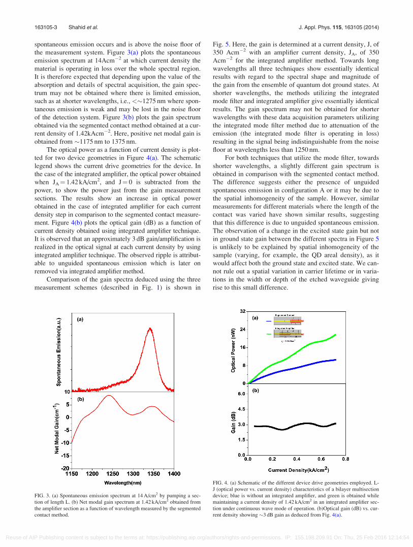
the measurement system. Figure 3(a) plots the spontaneous
emission spectrum at 14Acm�2 at which current density the
material is operating in loss over the whole spectral region.
It is therefore expected that depending upon the value of the
absorption and details of spectral acquisition, the gain spec-
trum may not be obtained where there is limited emission,
such as at shorter wavelengths, i.e., <�1275 nm where spon-
taneous emission is weak and may be lost in the noise floor
of the detection system. Figure 3(b) plots the gain spectrum
obtained via the segmented contact method obtained at a cur-
rent density of 1.42kAcm�2. Here, positive net modal gain is
obtained from �1175 nm to 1375 nm.
The optical power as a function of current density is plot-
ted for two device geometries in Figure 4(a). The schematic
legend shows the current drive geometries for the device. In
the case of the integrated amplifier, the optical power obtained
when JA¼ 1.42 kA/cm2, and J¼ 0 is subtracted from the
power, to show the power just from the gain measurement
sections. The results show an increase in optical power
obtained in the case of integrated amplifier for each current
density step in comparison to the segmented contact measure-
ment. Figure 4(b) plots the optical gain (dB) as a function of
current density obtained using integrated amplifier technique.
It is observed that an approximately 3 dB gain/amplification is
realized in the optical signal at each current density by using
integrated amplifier technique. The observed ripple is attribut-
able to unguided spontaneous emission which is later on
removed via integrated amplifier method.
Comparison of the gain spectra deduced using the three
measurement schemes (described in Fig. 1) is shown in
Fig. 5. Here, the gain is determined at a current density, J, of
350 Acm�2 with an amplifier current density, JA, of 350
Acm�2 for the integrated amplifier method. Towards long
wavelengths all three techniques show essentially identical
results with regard to the spectral shape and magnitude of
the gain from the ensemble of quantum dot ground states. At
shorter wavelengths, the methods utilizing the integrated
mode filter and integrated amplifier give essentially identical
results. The gain spectrum may not be obtained for shorter
wavelengths with these data acquisition parameters utilizing
the integrated mode filter method due to attenuation of the
emission (the integrated mode filter is operating in loss)
resulting in the signal being indistinguishable from the noise
floor at wavelengths less than 1250 nm.
For both techniques that utilize the mode filter, towards
shorter wavelengths, a slightly different gain spectrum is
obtained in comparison with the segmented contact method.
The difference suggests either the presence of unguided
spontaneous emission in configuration A or it may be due to
the spatial inhomogeneity of the sample. However, similar
measurements for different materials where the length of the
contact was varied have shown similar results, suggesting
that this difference is due to unguided spontaneous emission.
The observation of a change in the excited state gain but not
in ground state gain between the different spectra in Figure 5
is unlikely to be explained by spatial inhomogeneity of the
sample (varying, for example, the QD areal density), as it
would affect both the ground state and excited state. We can-
not rule out a spatial variation in carrier lifetime or in varia-
tions in the width or depth of the etched waveguide giving
rise to this small difference.
FIG. 3. (a) Spontaneous emission spectrum at 14 A/cm2 by pumping a sec-
tion of length L. (b) Net modal gain spectrum at 1.42 kA/cm2 obtained from
the amplifier section as a function of wavelength measured by the segmented
contact method.
FIG. 4. (a) Schematic of the different device drive geometries employed. L-
J (optical power vs. current density) characteristics of a bilayer multisection
device; blue is without an integrated amplifier, and green is obtained while
maintaining a current density of 1.42 kA/cm2 in an integrated amplifier sec-
tion under continuous wave mode of operation. (b)Optical gain (dB) vs. cur-
rent density showing �3 dB gain as deduced from Fig. 4(a).
163105-3 Shahid et al. J. Appl. Phys. 115, 163105 (2014)
Reuse of AIP Publishing content is subject to the terms at: https://publishing.aip.org/authors/rights-and-permissions. IP: 155.198.209.91 On: Thu, 25 Feb 2016 12:14:54
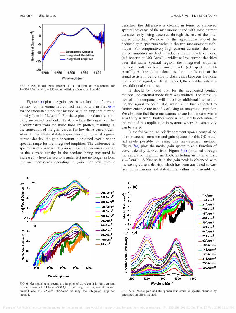
Figure 6(a) plots the gain spectra as a function of current
density for the segmented contact method and in Fig. 6(b)
for the integrated amplifier method with an amplifier current
density JA¼ 1.42 kAcm�2. For these plots, the data are man-
ually inspected, and only the data where the signal can be
discriminated from the noise floor are plotted, resulting in
the truncation of the gain curves for low drive current den-
sities. Under identical data acquisition conditions, at a given
current density, the gain spectrum is obtained over a wider
spectral range for the integrated amplifier. The difference in
spectral width over which gain is measured becomes smaller
as the current density in the sections being measured is
increased, where the sections under test are no longer in loss,
but are themselves operating in gain. For low current
densities, the difference is clearer, in terms of enhanced
spectral coverage of the measurement and with some current
densities only being accessed through the use of the inte-
grated amplifier. We note that the signal:noise ratio of the
deduced gain spectrum varies in the two measurement tech-
niques. For comparatively high current densities, the inte-
grated amplifier method introduces higher levels of noise
(c.f. spectra at 300 Acm�2), whilst at low current densities
over the same spectral region, the integrated amplifier
method results in lower noise levels (c.f. spectra at 14
Acm�2). At low current densities, the amplification of the
signal assists in being able to distinguish between the noise
floor and the signal, whilst at higher J, the amplifier introdu-
ces additional shot noise.
It should be noted that for the segmented contact
method, the external mode filter was omitted. The introduc-
tion of this component will introduce additional loss reduc-
ing the signal to noise ratio, which is in turn expected to
further enhance the benefits of using an integrated amplifier.
We also note that these measurements are for the case where
sensitivity is fixed. Further work is required to determine if
the method has application in systems where the sensitivity
can be varied.
In the following, we briefly comment upon a comparison
of spontaneous emission and gain spectra for this QD mate-
rial made possible by using this measurement method.
Figure 7(a) plots the modal gain spectrum as a function of
current density derived from Figure 6(b) (obtained through
the integrated amplifier method), including an internal loss,
ai¼ 2 cm�1. A blue-shift in the gain peak is observed with
increasing current density, which has been attributed to car-
rier thermalisation and state-filling within the ensemble of
FIG. 5. Net modal gain spectra as a function of wavelength for
J¼ 350 A/cm2 and JA¼ 350 A/cm2 utilizing schemes A, B, and C.
FIG. 6. Net modal gain spectra as a function of wavelength for (a) a current
density range of 14 A/cm2–300 A/cm2 utilizing the segmented contact
method and (b) 7A/cm2–300 A/cm2 utilizing the integrated amplifier
method.
FIG. 7. (a) Modal gain and (b) spontaneous emission spectra obtained by
integrated amplifier method.
163105-4 Shahid et al. J. Appl. Phys. 115, 163105 (2014)
Reuse of AIP Publishing content is subject to the terms at: https://publishing.aip.org/authors/rights-and-permissions. IP: 155.198.209.91 On: Thu, 25 Feb 2016 12:14:54

QDs.22 Figure 7(b) plots the spontaneous emission spectrum
over the same current densities, obtained using the same
method.9 By comparing the magnitude of the electrolumines-
cence when the QD ground-state is saturated, and that of the
lowest current density (7 Acm�2), we estimate that the aver-
age dot occupancy is �0.04 electron-hole pairs per QD.
Due to the low dot occupancy which can be accessed
using the integrated amplifer, the measurement of the gain/
absorption in conditions when the QDs are essentially empty,
yet under identical bias conditions is made possible. In Fig.
7(a)), a modal absorption of 9 61 cm�1 is measured for the
ground state. The saturated modal gain of the ground state
(at �300 A cm�2) is 761 cm�1. These values are very simi-
lar, which contrasts previous reports where absorption spec-
tra and gain spectra were compared under different bias
conditions,9,23 where very different values for absorption
and saturated gain were compared. Measurements of the
linewidth of the ground-state saturated gain and the absorp-
tion at the lowest current density give values of �50 nm for
gain (34 meV), whilst the absorption peak has a linewidth
of �35 nm (28 meV). We note that the product of linewidth
and absorption/gain is very similar in both cases (34� 7
¼ 238 meVcm�1, 28� 9¼ 252 meVcm�1. The difference in
the both line-width and absorption/saturated gain is attrib-
uted to the different possible carrier occupancies of the filled
quantum dot leading to an additional broadening mechanism
(due to different magnitudes of the free carrier shift of the
band-gap) which reduces the peak gain,6 as compared to the
peak absorption at these biases.
Figure 7(b) shows that as expected, at low current den-
sity, the spontaneous emission and absorption peak are
observed to be coincident (1338 nm/0.93 eV). The measure-
ment of the absorption peak at the positive biases where light
emission occurs is typically not reported. However, at high
current density, the spontaneous emission and peak in gain
do not coincide, with the gain peak being �4 meV smaller in
energy. Self-heating effects are identical in both cases as
these spectra are deduced from the same measurement. The
observation that the spontaneous emission does not signifi-
cantly shift in peak position from low occupancies (0.04 e-h
pairs per QD) to ground state saturation appears at odds with
the blue shift of the gain peak with increasing current den-
sity. If a thermalised carrier population is present, then a
blue-shift of the ground-state emission is also expected. A
possible explanation of the results is that there is a random
carrier population of the QDs, along with strong many-body
effects that modify the gain and spontaneous emission spec-
tra. A random carrier population would explain the essen-
tially identical QD ground-state EL spectra. Free carrier
effects, which shift the emission and gain of the QDs with
high electron-hole pair occupancy, may then give rise to the
observed blue-shift of the gain peak. In order to confirm this
tentative proposal, more sensitive measurements are
required. The analysis and theoretical modeling of EL and
gain/absorption spectra where the absorption peak is fully
resolved (and are obtained at even lower dot occupancies),
over a range of temperatures, are required.
V. CONCLUSIONS
In this paper, we have demonstrated the use of an inte-
grated amplifier and mode-filter in the measurement of
single-pass gain in semiconductor laser material. A direct
comparison of three segmented contact gain measurement
techniques has shown that for low current densities where
the material operates in loss, the gain can be measured over
a wider spectral region utilising the integrated amplifier.
Furthermore, the measurement of the gain spectrum at very
low current densities is made possible. We then discuss how
this method enables the analysis of gain/absorption and EL
spectra of QDs at very low dot occupancies, which may, in
future, cast light on fundamental physical processes.
ACKNOWLEDGMENTS
This work was funded under EPSRC Grant No.
EP/FO3427X/1. H. Shahid gratefully acknowledges support
from the University of Engineering and Technology (K.S.K.
campus), Lahore, Punjab, Pakistan.
1P. W. A. Mc Ilroy, A. Kurobe, and Y. Uematsu, IEEE J. Quantum
Electron. 21, 1958 (1985).2Y. Arakawa and A. Yariv, IEEE J. Quantum Electron. 22, 1887 (1986).3M. J. Connelly, IEEE J. Quantum Electron. 37, 439 (2001).4G. A. Alphonse, G. B. Gilbert, M. G. Harvey, and M. Ettenberg, IEEE J.
Quantum Electron. 24, 2454 (1988).5B. W. Hakki and T. L. Paoli, J. Appl. Phys. 46, 1299 (1975).6H. Shahid, D. T. D. Childs, B. J. Stevens, and R. A. Hogg, Appl. Phys.
Lett. 99, 061104 (2011).7K. L. Shaklee and R. F. Leheny, Appl. Phys. Lett. 46, 475 (1971).8A. Oster, G. Erbert, and H. Wenzel, Electron. Lett. 33, 864 (1997).9P. Blood, G. M. Lewis, P. M. Smowton, H. D. Summers, J. D. Thomson,
and J. Lutti, IEEE J. Sel. Top. Quantum Electron. 9, 1275 (2003).10Y. C. Xin, Y. Li, A. Martinez, T. J. Rotter, H. Su, L. Zhang, A. L. Gray, S.
Luong, K. Sun, Z. Zou, J. Zilko, P. M. Varangis, and L. F. Lester, IEEE J.
Quantum Electron. 42, 725 (2006).11K. Otsubo, N. Hatori, M. Ishida, S. Okumura, T. Akiyama, Y. Nakata, H.
Ebe, M. Sugawara, and Y. Arakawa, Jpn. J. Appl. Phys. 43, 1124 (2004).12S. Fathpour, Z. Mi, P. Bhattacharya, A. Kovsh, S. Mikhrin, I. Krestnikov,
A. Kozhukhov, and N. Ledentsov, Appl. Phys. Lett 85, 5164 (2004).13P. D. L. Greenwood, D. T. D. Childs, K. Kennedy, K. M. Groom, M.
Hugues, M. Hopkinson, R. A. Hogg, N. Krstajic, L. E. Smith, S. J.
Matcher, M. Bonesi, S. MacNeil, and R. Smallwood, IEEE J. Sel. Top.
Quantum Electron. 16, 1015 (2010).14E. U. Rafailov, M. A. Cataluna, and W. Sibbett, Nat. Photonics 1, 395 (2007).15K. Takada, M. Ishida, Y. Nakata, T. Yamamoto, M. Yamaguchi, K. Nishi,
M. Sugawara, and Y. Arakawa, IEEE Asia Commun. Photon. Conf. Exhib.
2010, 577.16M. Sugawara, K. Mukai, Y. Nakata, and H. Ishikawa, Phys. Rev. B 61,
7595 (2000).17A. Markus, J. X. Chen, O. Gauthier-Lafaye, J.-G. Provost, C. Parantho€en,
and A. Fiore, IEEE J. Sel. Top. Quantum Electron. 9, 1308 (2003).18I. O’Driscoll, M. Hutchings, P. M. Smowton, and P. Blood, Appl. Phys.
Lett. 97, 141102 (2010).19E. C. Le Ru, P. Howe, T. S. Jones, and R. Murray, Phys. Rev. B 67,
165303 (2003).20P. Howe, E. C. Le Ru, E. Clarke, B. Abbey, R. Murray, and T. S. Jones,
J. Appl. Phys. 95, 2998 (2004).21M. A. Majid, D. T. D. Childs, H. Shahid, S. C. Chen, K. Kennedy, R. J.
Airey, R. A. Hogg, E. Clarke, P. Spencer, and R. Murray, Jpn. J. Appl.
Phys., Part 2 50, 04DG10-1 (2011).22R. Heitz, F. Guffarth, I. Mukhametzhanov, M. Grundmann, A. Madhukar,
and D. Bimberg, Phys. Rev. B 62, 16881 (2000).23I. C. Sandall, C. L. Walker, P. M. Smowton, D. J. Mowbray, and H. Y.
Liu, IEE Proc.–J: Optoelectron. 153, 316 (2006).
163105-5 Shahid et al. J. Appl. Phys. 115, 163105 (2014)
Reuse of AIP Publishing content is subject to the terms at: https://publishing.aip.org/authors/rights-and-permissions. IP: 155.198.209.91 On: Thu, 25 Feb 2016 12:14:54