Embed Size (px)
Citation preview
Copyright © Bridgetek Pte Ltd 1
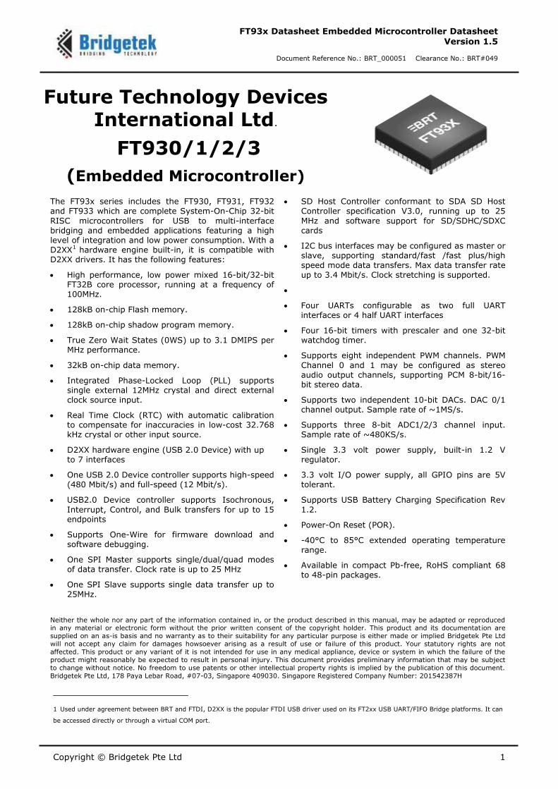
FT93x Datasheet Embedded Microcontroller Datasheet Version 1.5
Document Reference No.: BRT_000051 Clearance No.: BRT#049
Future Technology Devices International Ltd.
FT930/1/2/3
(Embedded Microcontroller)
The FT93x series includes the FT930, FT931, FT932 and FT933 which are complete System-On-Chip 32-bit
RISC microcontrollers for USB to multi-interface bridging and embedded applications featuring a high level of integration and low power consumption. With a D2XX1 hardware engine built-in, it is compatible with D2XX drivers. It has the following features:
High performance, low power mixed 16-bit/32-bit FT32B core processor, running at a frequency of 100MHz.
128kB on-chip Flash memory.
128kB on-chip shadow program memory.
True Zero Wait States (0WS) up to 3.1 DMIPS per MHz performance.
32kB on-chip data memory.
Integrated Phase-Locked Loop (PLL) supports single external 12MHz crystal and direct external clock source input.
Real Time Clock (RTC) with automatic calibration to compensate for inaccuracies in low-cost 32.768 kHz crystal or other input source.
D2XX hardware engine (USB 2.0 Device) with up to 7 interfaces
One USB 2.0 Device controller supports high-speed (480 Mbit/s) and full-speed (12 Mbit/s).
USB2.0 Device controller supports Isochronous,
Interrupt, Control, and Bulk transfers for up to 15 endpoints
Supports One-Wire for firmware download and software debugging.
One SPI Master supports single/dual/quad modes of data transfer. Clock rate is up to 25 MHz
One SPI Slave supports single data transfer up to 25MHz.
SD Host Controller conformant to SDA SD Host Controller specification V3.0, running up to 25
MHz and software support for SD/SDHC/SDXC cards
I2C bus interfaces may be configured as master or slave, supporting standard/fast /fast plus/high speed mode data transfers. Max data transfer rate up to 3.4 Mbit/s. Clock stretching is supported.
Four UARTs configurable as two full UART interfaces or 4 half UART interfaces
Four 16-bit timers with prescaler and one 32-bit watchdog timer.
Supports eight independent PWM channels. PWM
Channel 0 and 1 may be configured as stereo audio output channels, supporting PCM 8-bit/16-bit stereo data.
Supports two independent 10-bit DACs. DAC 0/1 channel output. Sample rate of ~1MS/s.
Supports three 8-bit ADC1/2/3 channel input. Sample rate of ~480KS/s.
Single 3.3 volt power supply, built-in 1.2 V regulator.
3.3 volt I/O power supply, all GPIO pins are 5V tolerant.
Supports USB Battery Charging Specification Rev
1.2.
Power-On Reset (POR).
-40°C to 85°C extended operating temperature range.
Available in compact Pb-free, RoHS compliant 68 to 48-pin packages.
Neither the whole nor any part of the information contained in, or the product described in this manual, may be adapted or reproduced in any material or electronic form without the prior written consent of the copyright holder. This product and its documentation are
supplied on an as-is basis and no warranty as to their suitability for any particular purpose is either made or implied Bridgetek Pte Ltd
will not accept any claim for damages howsoever arising as a result of use or failure of this product. Your statutory rights are not
affected. This product or any variant of it is not intended for use in any medical appliance, device or system in which the failure of the
product might reasonably be expected to result in personal injury. This document provides preliminary information that may be subject
to change without notice. No freedom to use patents or other intellectual property rights is implied by the publication of this document.
Bridgetek Pte Ltd, 178 Paya Lebar Road, #07-03, Singapore 409030. Singapore Registered Company Number: 201542387H
1 Used under agreement between BRT and FTDI, D2XX is the popular FTDI USB driver used on its FT2xx USB UART/FIFO Bridge platforms. It can
be accessed directly or through a virtual COM port.
Copyright © Bridgetek Pte Ltd 2
FT93x Datasheet Embedded Microcontroller Datasheet Version 1.5
Document Reference No.: BRT_000051 Clearance No.: BRT#049
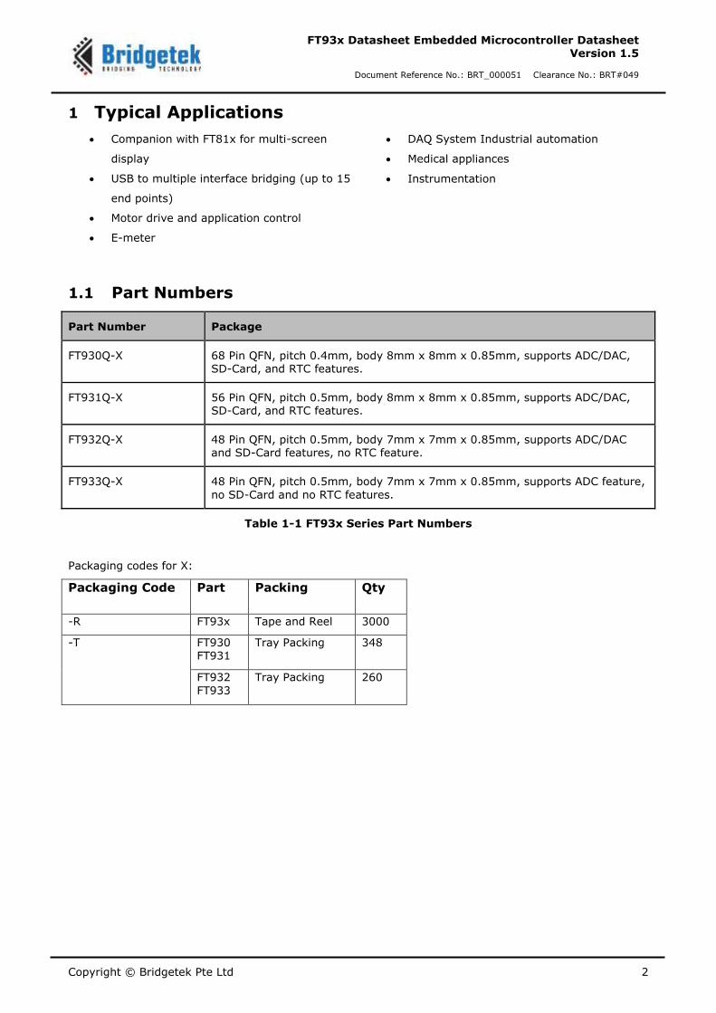
1 Typical Applications
Companion with FT81x for multi-screen
display
USB to multiple interface bridging (up to 15
end points)
Motor drive and application control
E-meter
DAQ System Industrial automation
Medical appliances
Instrumentation
1.1 Part Numbers
Part Number Package
FT930Q-X 68 Pin QFN, pitch 0.4mm, body 8mm x 8mm x 0.85mm, supports ADC/DAC, SD-Card, and RTC features.
FT931Q-X 56 Pin QFN, pitch 0.5mm, body 8mm x 8mm x 0.85mm, supports ADC/DAC, SD-Card, and RTC features.
FT932Q-X 48 Pin QFN, pitch 0.5mm, body 7mm x 7mm x 0.85mm, supports ADC/DAC and SD-Card features, no RTC feature.
FT933Q-X 48 Pin QFN, pitch 0.5mm, body 7mm x 7mm x 0.85mm, supports ADC feature,
no SD-Card and no RTC features.
Table 1-1 FT93x Series Part Numbers
Packaging codes for X:
Packaging Code Part Packing Qty
-R FT93x Tape and Reel 3000
-T FT930 FT931
Tray Packing 348
FT932
FT933
Tray Packing 260
Copyright © Bridgetek Pte Ltd 3
FT93x Datasheet Embedded Microcontroller Datasheet Version 1.5
Document Reference No.: BRT_000051 Clearance No.: BRT#049
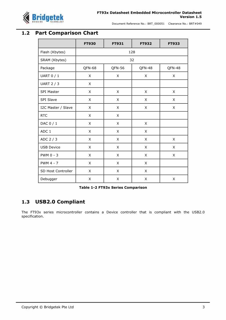
1.2 Part Comparison Chart
FT930 FT931 FT932 FT933
Flash (Kbytes) 128
SRAM (Kbytes) 32
Package QFN-68 QFN-56 QFN-48 QFN-48
UART 0 / 1 X X X X
UART 2 / 3 X
SPI Master X X X X
SPI Slave X X X X
I2C Master / Slave X X X X
RTC X X
DAC 0 / 1 X X X
ADC 1 X X X
ADC 2 / 3 X X X X
USB Device X X X X
PWM 0 - 3 X X X X
PWM 4 - 7 X X X
SD Host Controller X X X
Debugger X X X X
Table 1-2 FT93x Series Comparison
1.3 USB2.0 Compliant
The FT93x series microcontroller contains a Device controller that is compliant with the USB2.0 specification.
Copyright © Bridgetek Pte Ltd 4
FT93x Datasheet Embedded Microcontroller Datasheet Version 1.5
Document Reference No.: BRT_000051 Clearance No.: BRT#049
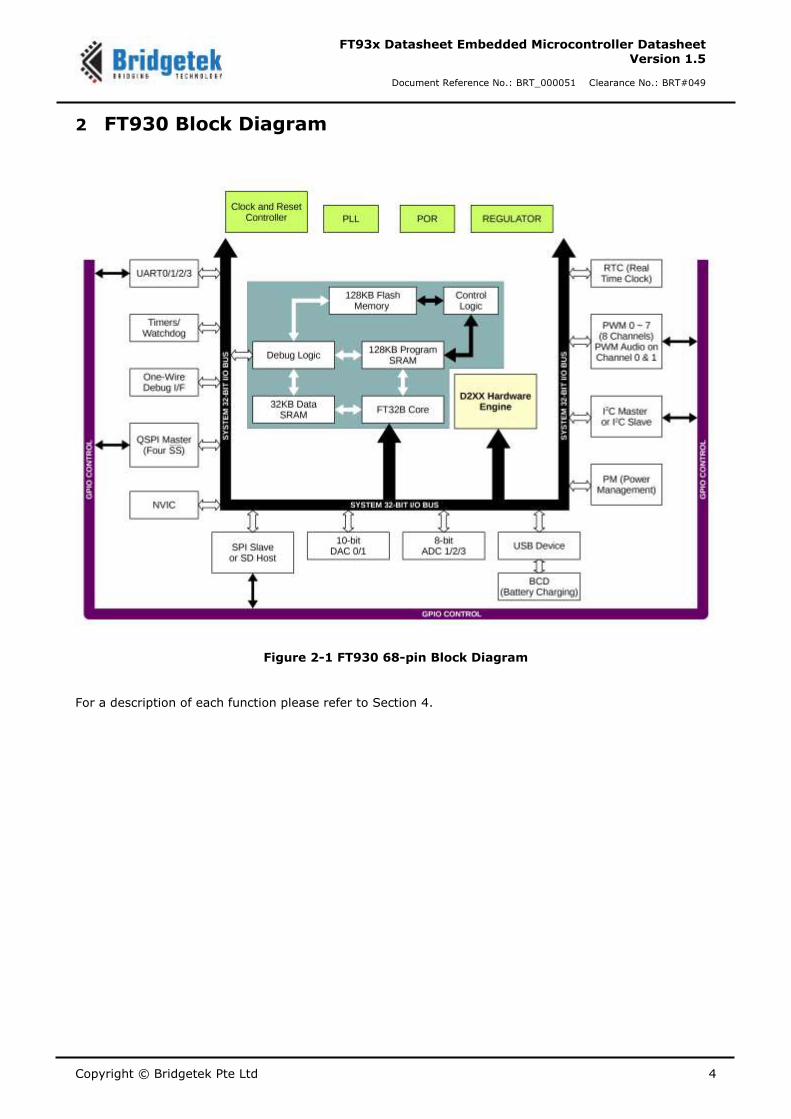
2 FT930 Block Diagram
Figure 2-1 FT930 68-pin Block Diagram
For a description of each function please refer to Section 4.
Copyright © Bridgetek Pte Ltd 5
FT93x Datasheet Embedded Microcontroller Datasheet Version 1.5
Document Reference No.: BRT_000051 Clearance No.: BRT#049
Table of Contents
1 Typical Applications ....................................................... 2
1.1 Part Numbers ............................................................................. 2
1.2 Part Comparison Chart ............................................................... 3
1.3 USB2.0 Compliant ...................................................................... 3
2 FT930 Block Diagram .................................................... 4
3 Device Pinout and Signal Description ............................ 8
3.1 FT930 QFN68 Pinout .................................................................. 8
3.2 FT931 QFN56 Pinout .................................................................. 9
3.3 FT932 QFN48 Pinout ................................................................ 10
3.4 FT933 QFN48 Pinout ................................................................ 11
3.5 FT930 Pin Description .............................................................. 12
3.6 FT931 Pin Description .............................................................. 18
3.7 FT932 Pin Description .............................................................. 23
3.8 FT933 Pin Description .............................................................. 27
4 Function Description ................................................... 31
4.1 Architectural Overview ............................................................ 31
4.2 FT32B Core Processor .............................................................. 31
4.3 D2XX Hardware Engine ............................................................ 31
4.4 128kB Flash Memory ................................................................ 32
4.5 Boot Sequence ......................................................................... 32
4.6 Interrupt .................................................................................. 32
4.7 Memory Mapping...................................................................... 33
4.8 USB2.0 Device Contoller .......................................................... 34
4.8.1 Features .................................................................................................. 34
4.9 Real Time Clock ....................................................................... 35
4.9.1 Features .................................................................................................. 35
4.10 One-Wire Debugger Interface ............................................... 35
4.10.1 Features .................................................................................................. 35
4.11 SPI Interface ......................................................................... 35
4.11.1 Features .................................................................................................. 35
4.12 I2C Interface ......................................................................... 36
4.12.1 Features .................................................................................................. 36
4.13 UART Interface ...................................................................... 36
Copyright © Bridgetek Pte Ltd 6
FT93x Datasheet Embedded Microcontroller Datasheet Version 1.5
Document Reference No.: BRT_000051 Clearance No.: BRT#049
4.13.1 Features .................................................................................................. 36
4.14 Timers and Watchdog Timer .................................................. 36
4.14.1 Features .................................................................................................. 37
4.15 PWM ...................................................................................... 37
4.15.1 Features .................................................................................................. 37
4.16 SD Host Controller ................................................................. 38
4.16.1 Features .................................................................................................. 38
4.17 Analog to Digital Converter (ADC) ......................................... 38
4.17.1 Features .................................................................................................. 38
4.18 Digital to Analog Converter (DAC) ......................................... 38
4.18.1 Features .................................................................................................. 38
4.19 General Purpose Input Output............................................... 39
4.19.1 Features .................................................................................................. 39
4.20 System Clocks ....................................................................... 39
4.20.1 12MHz Oscillator ....................................................................................... 39
4.20.2 Phase Locked Loop .................................................................................... 39
4.20.3 32.768 kHz RTC Oscillator .......................................................................... 39
4.20.4 Internal Slow Clock Oscillator ..................................................................... 39
4.21 Power Management ............................................................... 40
4.21.1 Power Supply ........................................................................................... 40
4.21.2 Power down Mode ..................................................................................... 40
5 Device Characteristics and Ratings .............................. 41
5.1 Absolute Maximum Ratings ...................................................... 41
5.2 DC Characteristics .................................................................... 42
5.3 AC Characteristics .................................................................... 44
5.4 8-bit ADC Converter ................................................................. 50
5.5 10-bit DAC Converter ............................................................... 50
6 Application Information .............................................. 51
6.1 Crystal Oscillator ..................................................................... 51
6.1.1 Crystal oscillator application circuit .............................................................. 51
6.1.2 External clock input ................................................................................... 51
6.2 RTC Oscillator .......................................................................... 52
6.3 Standard I/O Pin Configuration ............................................... 52
6.4 USB2.0 Device Interface .......................................................... 53
6.5 USB Connection when Unused (FT93x) .................................... 54
7 Package Parameters .................................................... 55
Copyright © Bridgetek Pte Ltd 7
FT93x Datasheet Embedded Microcontroller Datasheet Version 1.5
Document Reference No.: BRT_000051 Clearance No.: BRT#049
7.1 QFN-68 Package Dimensions ................................................... 56
7.2 QFN-56 Package Dimensions ................................................... 57
7.3 QFN-48 Package Dimensions ................................................... 58
7.4 QFN-68/56/48 Device Marking ................................................ 59
7.4.1 FT93XQ Top Side ...................................................................................... 59
7.5 Solder Reflow Profile ............................................................... 60
8 Contact Information .................................................... 61
Appendix A – References ................................................... 62
Document References ...................................................................... 62
Acronyms and Abbreviations ............................................................ 62
Appendix B - List of Figures and Tables ............................. 63
List of Figures .................................................................................. 63
List of Tables .................................................................................... 64
Appendix C - Revision History ............................................ 65
Copyright © Bridgetek Pte Ltd 8
FT93x Datasheet Embedded Microcontroller Datasheet Version 1.5
Document Reference No.: BRT_000051 Clearance No.: BRT#049
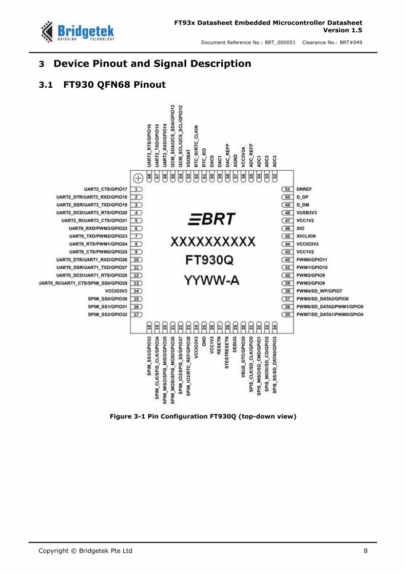
3 Device Pinout and Signal Description
3.1 FT930 QFN68 Pinout
Figure 3-1 Pin Configuration FT930Q (top-down view)
Copyright © Bridgetek Pte Ltd 9
FT93x Datasheet Embedded Microcontroller Datasheet Version 1.5
Document Reference No.: BRT_000051 Clearance No.: BRT#049
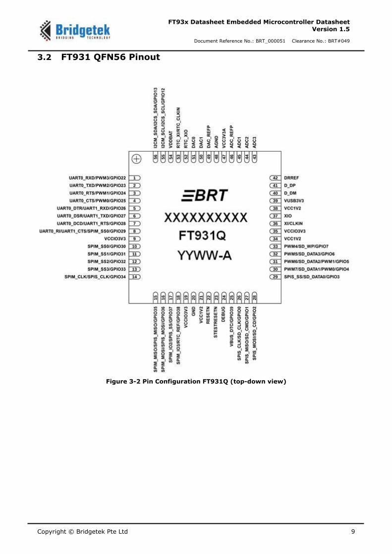
3.2 FT931 QFN56 Pinout
Figure 3-2 Pin Configuration FT931Q (top-down view)
Copyright © Bridgetek Pte Ltd 10
FT93x Datasheet Embedded Microcontroller Datasheet Version 1.5
Document Reference No.: BRT_000051 Clearance No.: BRT#049
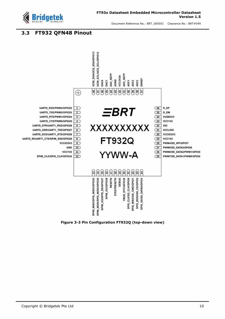
3.3 FT932 QFN48 Pinout
Figure 3-3 Pin Configuration FT932Q (top-down view)
Copyright © Bridgetek Pte Ltd 11
FT93x Datasheet Embedded Microcontroller Datasheet Version 1.5
Document Reference No.: BRT_000051 Clearance No.: BRT#049
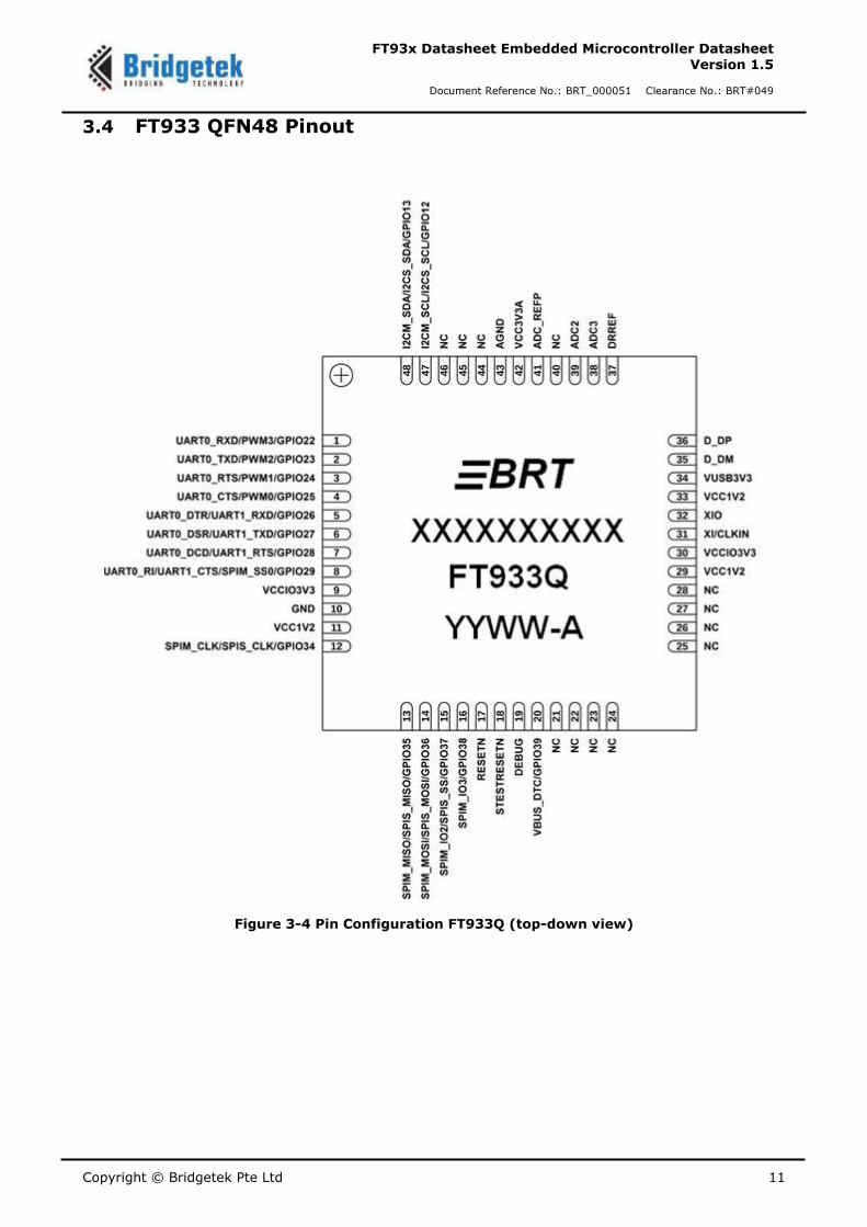
3.4 FT933 QFN48 Pinout
Figure 3-4 Pin Configuration FT933Q (top-down view)
Copyright © Bridgetek Pte Ltd 12
FT93x Datasheet Embedded Microcontroller Datasheet Version 1.5
Document Reference No.: BRT_000051 Clearance No.: BRT#049
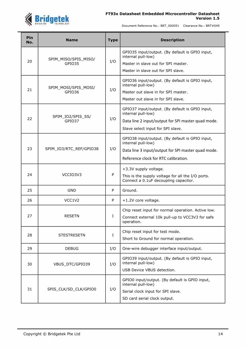
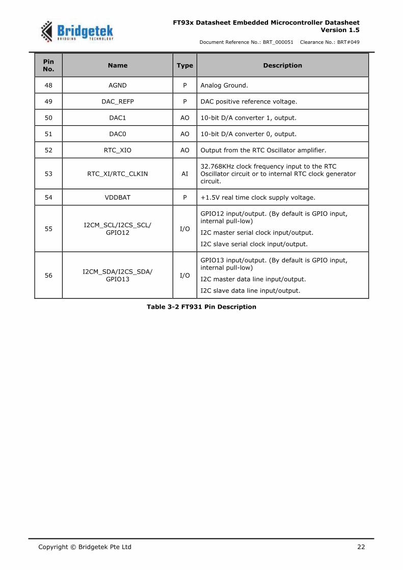
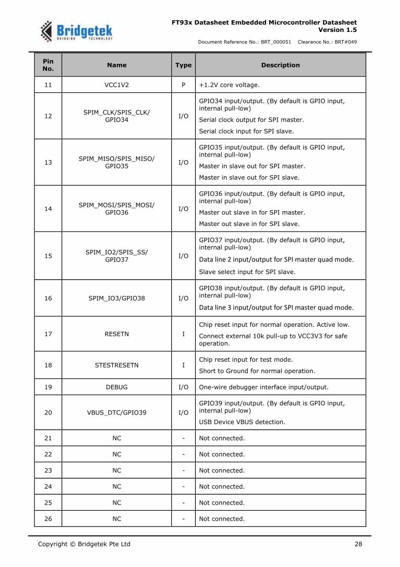
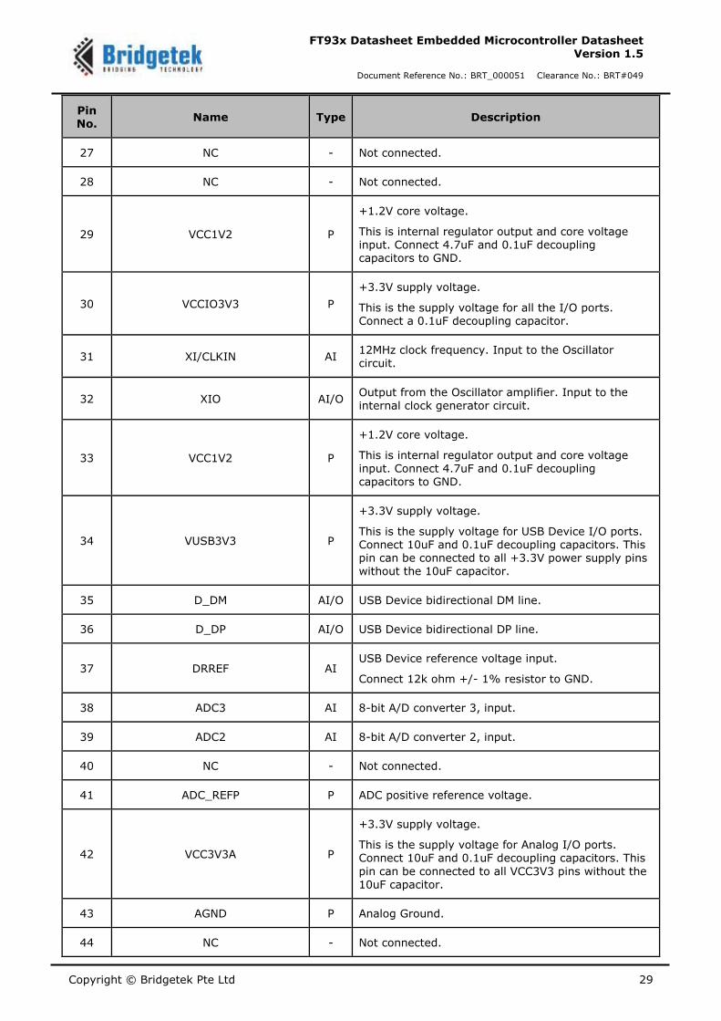
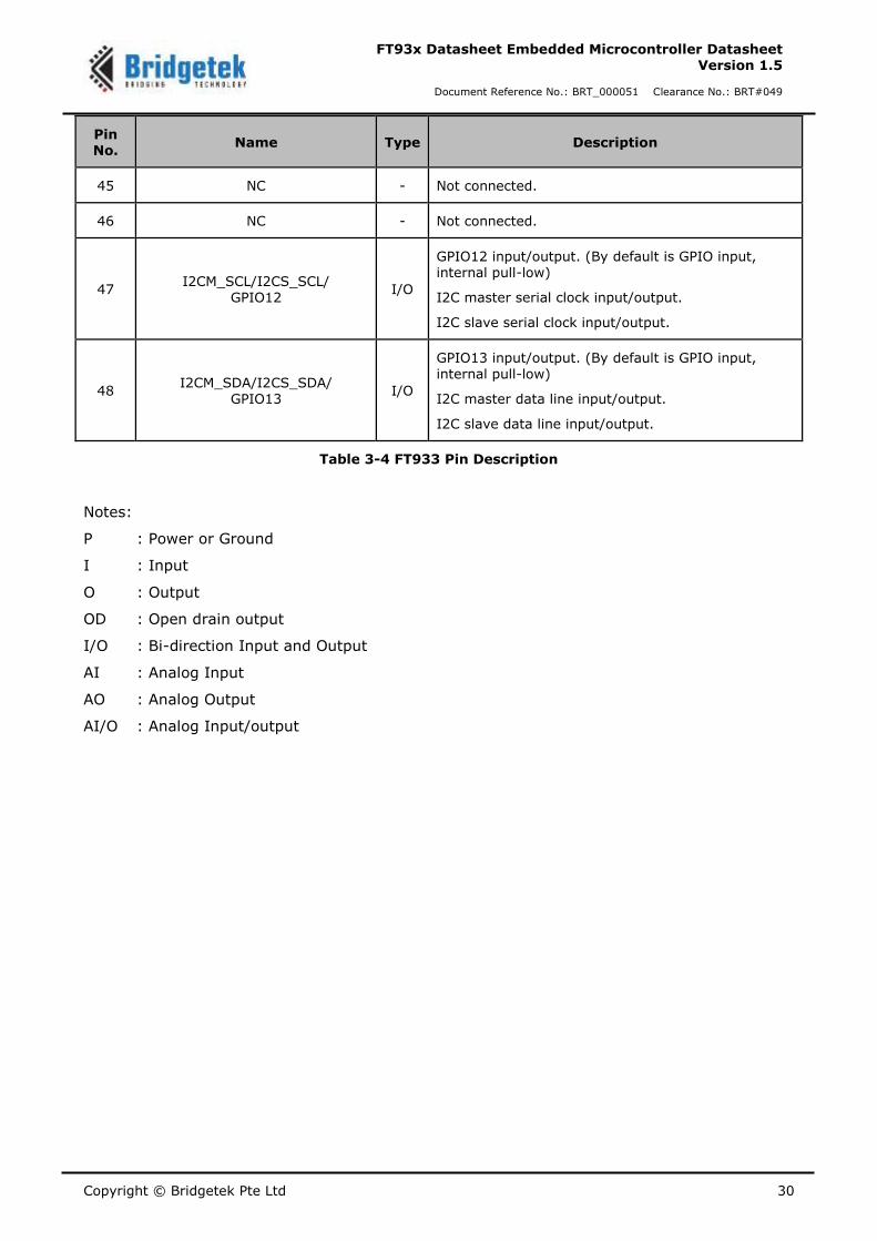
3.5 FT930 Pin Description
Pin
No. Name Type Description
1 UART2_CTS/GPIO17 I/O
GPIO17 input/output. (By default is GPIO input, internal pull-low)
Clear to send input for UART2.
2 UART2_DTR/UART3_RXD/
GPIO18 I/O
GPIO18 input/output. (By default is GPIO input, internal pull-low)
Data terminal ready output for UART2.
Receiver input for UART3.
3 UART2_DSR/UART3_TXD/
GPIO19 I/O
GPIO19 input/output. (By default is GPIO input,
internal pull-low)
Data set ready input for UART2
Transmitter output for UART3.
4 UART2_DCD/UART3_RTS/
GPIO20 I/O
GPIO20 input/output. (By default is GPIO input, internal pull-low)
Data carrier detection input for UART2
Request to send output for UART3.
5 UART2_RI/UART3_CTS/
GPIO21 I/O
GPIO21 input/output. (By default is GPIO input, internal pull-low)
Ring indicator input for UART2.
Clear to send input for UART3.
6 UART0_RXD/PWM3/
GPIO22 I/O
GPIO22 input/output. (By default is GPIO input, internal pull-low)
Receiver input for UART0.
PWM channel 3, output.
7 UART0_TXD/PWM2/
GPIO23 I/O
GPIO23 input/output. (By default is GPIO input, internal pull-low)
Transmitter output for UART0.
PWM channel 2, output.
8 UART0_RTS/PWM1/
GPIO24 I/O
GPIO24 input/output. (By default is GPIO input, internal pull-low)
Request to send output for UART0.
PWM channel 1, output.
9 UART0_CTS/PWM0/
GPIO25 I/O
GPIO25 input/output. (By default is GPIO input,
internal pull-low)
Clear to send input for UART0.
PWM channel 0, output.
Copyright © Bridgetek Pte Ltd 13
FT93x Datasheet Embedded Microcontroller Datasheet Version 1.5
Document Reference No.: BRT_000051 Clearance No.: BRT#049
Pin No.
Name Type Description
10 UART0_DTR/UART1_RXD/
GPIO26 I/O
GPIO26 input/output. (By default is GPIO input, internal pull-low)
Data terminal ready output for UART0.
Receiver input for UART1.
11 UART0_DSR/UART1_TXD/
GPIO27 I/O
GPIO27 input/output. (By default is GPIO input, internal pull-low)
Data set ready input for UART0
Transmitter output for UART1.
12 UART0_DCD/UART1_RTS/
GPIO28 I/O
GPIO28 input/output. (By default is GPIO input,
internal pull-low)
Data carrier detection input for UART0.
Request to send output for UART1.
13 UART0_RI/UART1_CTS/
SPIM_SS0/GPIO29 I/O
GPIO29 input/output. (By default is GPIO input,
internal pull-low)
Ring indicator input for UART0.
Clear to send input for UART1.
Slave select 0 output for SPI master.
14 VCCIO3V3 P
+3.3V supply voltage.
This is the supply voltage for all the I/O ports. Connect a 0.1uF decoupling capacitor.
15 SPIM_SS0/GPIO30 I/O
GPIO30 input/output. (By default is GPIO input, internal pull-low)
Slave select 0 output for SPI master.
16 SPIM_SS1/GPIO31 I/O
GPIO31 input/output. (By default is GPIO input, internal pull-low)
Slave select 1 output for SPI master.
17 SPIM_SS2/GPIO32 I/O
GPIO32 input/output. (By default is GPIO input, internal pull-low)
Slave select 2 output for SPI master.
18 SPIM_SS3/GPIO33 I/O
GPIO33 input/output. (By default is GPIO input, internal pull-low)
Slave select 3 output for SPI master.
19 SPIM_CLK/SPIS_CLK/
GPIO34 I/O
GPIO34 input/output. (By default is GPIO input,
internal pull-low)
Serial clock output for SPI master.
Serial clock input for SPI slave.
Copyright © Bridgetek Pte Ltd 14
FT93x Datasheet Embedded Microcontroller Datasheet Version 1.5
Document Reference No.: BRT_000051 Clearance No.: BRT#049
Pin No.
Name Type Description
20 SPIM_MISO/SPIS_MISO/
GPIO35 I/O
GPIO35 input/output. (By default is GPIO input, internal pull-low)
Master in slave out for SPI master.
Master in slave out for SPI slave.
21 SPIM_MOSI/SPIS_MOSI/
GPIO36 I/O
GPIO36 input/output. (By default is GPIO input, internal pull-low)
Master out slave in for SPI master.
Master out slave in for SPI slave.
22 SPIM_IO2/SPIS_SS/
GPIO37 I/O
GPIO37 input/output. (By default is GPIO input,
internal pull-low)
Data line 2 input/output for SPI master quad mode.
Slave select input for SPI slave.
23 SPIM_IO3/RTC_REF/GPIO38 I/O
GPIO38 input/output. (By default is GPIO input, internal pull-low)
Data line 3 input/output for SPI master quad mode.
Reference clock for RTC calibration.
24 VCCIO3V3 P
+3.3V supply voltage.
This is the supply voltage for all the I/O ports. Connect a 0.1uF decoupling capacitor.
25 GND P Ground.
26 VCC1V2 P +1.2V core voltage.
27 RESETN I
Chip reset input for normal operation. Active low.
Connect external 10k pull-up to VCC3V3 for safe operation.
28 STESTRESETN I Chip reset input for test mode.
Short to Ground for normal operation.
29 DEBUG I/O One-wire debugger interface input/output.
30 VBUS_DTC/GPIO39 I/O
GPIO39 input/output. (By default is GPIO input, internal pull-low)
USB Device VBUS detection.
31 SPIS_CLK/SD_CLK/GPIO0 I/O
GPIO0 input/output. (By default is GPIO input, internal pull-low)
Serial clock input for SPI slave.
SD card serial clock output.
Copyright © Bridgetek Pte Ltd 15
FT93x Datasheet Embedded Microcontroller Datasheet Version 1.5
Document Reference No.: BRT_000051 Clearance No.: BRT#049
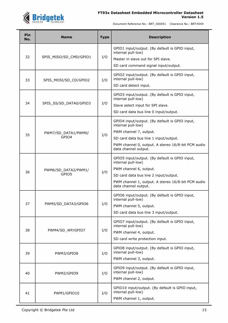
Pin No.
Name Type Description
32 SPIS_MISO/SD_CMD/GPIO1 I/O
GPIO1 input/output. (By default is GPIO input, internal pull-low)
Master in slave out for SPI slave.
SD card command signal input/output.
33 SPIS_MOSI/SD_CD/GPIO2 I/O
GPIO2 input/output. (By default is GPIO input, internal pull-low)
SD card detect input.
34 SPIS_SS/SD_DATA0/GPIO3 I/O
GPIO3 input/output. (By default is GPIO input, internal pull-low)
Slave select input for SPI slave.
SD card data bus line 0 input/output.
35 PWM7/SD_DATA1/PWM0/
GPIO4 I/O
GPIO4 input/output. (By default is GPIO input, internal pull-low)
PWM channel 7, output.
SD card data bus line 1 input/output.
PWM channel 0, output. A stereo 16/8-bit PCM audio data channel output.
36 PWM6/SD_DATA2/PWM1/
GPIO5 I/O
GPIO5 input/output. (By default is GPIO input, internal pull-low)
PWM channel 6, output.
SD card data bus line 2 input/output.
PWM channel 1, output. A stereo 16/8-bit PCM audio data channel output.
37 PWM5/SD_DATA3/GPIO6 I/O
GPIO6 input/output. (By default is GPIO input, internal pull-low)
PWM channel 5, output.
SD card data bus line 3 input/output.
38 PWM4/SD_WP/GPIO7 I/O
GPIO7 input/output. (By default is GPIO input, internal pull-low)
PWM channel 4, output.
SD card write protection input.
39 PWM3/GPIO8 I/O
GPIO8 input/output. (By default is GPIO input,
internal pull-low)
PWM channel 3, output.
40 PWM2/GPIO9 I/O
GPIO9 input/output. (By default is GPIO input,
internal pull-low)
PWM channel 2, output.
41 PWM1/GPIO10 I/O
GPIO10 input/output. (By default is GPIO input, internal pull-low)
PWM channel 1, output.
Copyright © Bridgetek Pte Ltd 16
FT93x Datasheet Embedded Microcontroller Datasheet Version 1.5
Document Reference No.: BRT_000051 Clearance No.: BRT#049
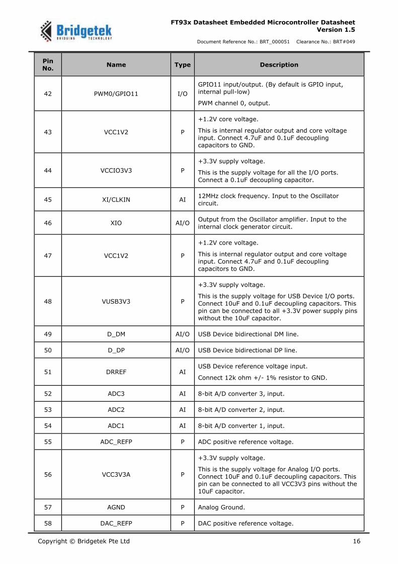
Pin No.
Name Type Description
42 PWM0/GPIO11 I/O
GPIO11 input/output. (By default is GPIO input, internal pull-low)
PWM channel 0, output.
43 VCC1V2 P
+1.2V core voltage.
This is internal regulator output and core voltage input. Connect 4.7uF and 0.1uF decoupling capacitors to GND.
44 VCCIO3V3 P
+3.3V supply voltage.
This is the supply voltage for all the I/O ports.
Connect a 0.1uF decoupling capacitor.
45 XI/CLKIN AI 12MHz clock frequency. Input to the Oscillator circuit.
46 XIO AI/O Output from the Oscillator amplifier. Input to the internal clock generator circuit.
47 VCC1V2 P
+1.2V core voltage.
This is internal regulator output and core voltage input. Connect 4.7uF and 0.1uF decoupling capacitors to GND.
48 VUSB3V3 P
+3.3V supply voltage.
This is the supply voltage for USB Device I/O ports.
Connect 10uF and 0.1uF decoupling capacitors. This pin can be connected to all +3.3V power supply pins
without the 10uF capacitor.
49 D_DM AI/O USB Device bidirectional DM line.
50 D_DP AI/O USB Device bidirectional DP line.
51 DRREF AI USB Device reference voltage input.
Connect 12k ohm +/- 1% resistor to GND.
52 ADC3 AI 8-bit A/D converter 3, input.
53 ADC2 AI 8-bit A/D converter 2, input.
54 ADC1 AI 8-bit A/D converter 1, input.
55 ADC_REFP P ADC positive reference voltage.
56 VCC3V3A P
+3.3V supply voltage.
This is the supply voltage for Analog I/O ports. Connect 10uF and 0.1uF decoupling capacitors. This pin can be connected to all VCC3V3 pins without the
10uF capacitor.
57 AGND P Analog Ground.
58 DAC_REFP P DAC positive reference voltage.
Copyright © Bridgetek Pte Ltd 17
FT93x Datasheet Embedded Microcontroller Datasheet Version 1.5
Document Reference No.: BRT_000051 Clearance No.: BRT#049
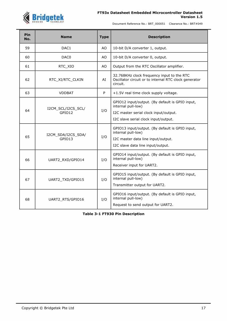
Pin No.
Name Type Description
59 DAC1 AO 10-bit D/A converter 1, output.
60 DAC0 AO 10-bit D/A converter 0, output.
61 RTC_XIO AO Output from the RTC Oscillator amplifier.
62 RTC_XI/RTC_CLKIN AI 32.768KHz clock frequency input to the RTC Oscillator circuit or to internal RTC clock generator circuit.
63 VDDBAT P +1.5V real time clock supply voltage.
64 I2CM_SCL/I2CS_SCL/
GPIO12 I/O
GPIO12 input/output. (By default is GPIO input, internal pull-low)
I2C master serial clock input/output.
I2C slave serial clock input/output.
65 I2CM_SDA/I2CS_SDA/
GPIO13 I/O
GPIO13 input/output. (By default is GPIO input, internal pull-low)
I2C master data line input/output.
I2C slave data line input/output.
66 UART2_RXD/GPIO14 I/O
GPIO14 input/output. (By default is GPIO input, internal pull-low)
Receiver input for UART2.
67 UART2_TXD/GPIO15 I/O
GPIO15 input/output. (By default is GPIO input,
internal pull-low)
Transmitter output for UART2.
68 UART2_RTS/GPIO16 I/O
GPIO16 input/output. (By default is GPIO input, internal pull-low)
Request to send output for UART2.
Table 3-1 FT930 Pin Description
Copyright © Bridgetek Pte Ltd 18
FT93x Datasheet Embedded Microcontroller Datasheet Version 1.5
Document Reference No.: BRT_000051 Clearance No.: BRT#049
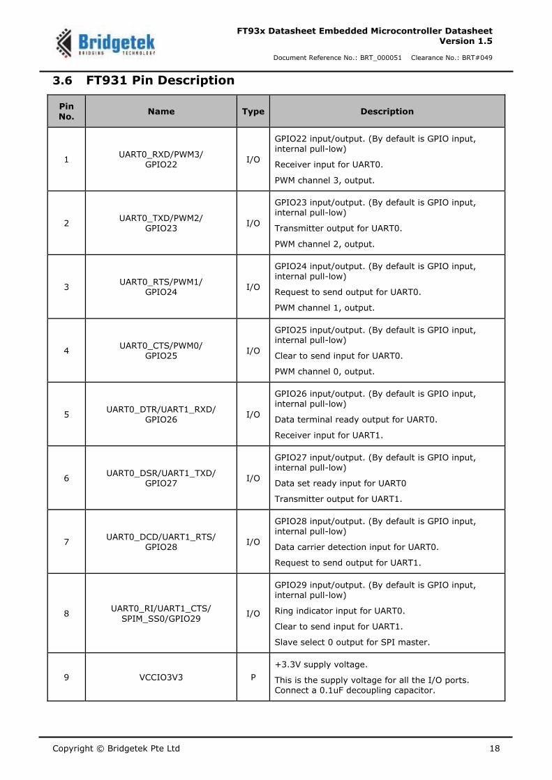
3.6 FT931 Pin Description
Pin
No. Name Type Description
1 UART0_RXD/PWM3/
GPIO22 I/O
GPIO22 input/output. (By default is GPIO input, internal pull-low)
Receiver input for UART0.
PWM channel 3, output.
2 UART0_TXD/PWM2/
GPIO23 I/O
GPIO23 input/output. (By default is GPIO input, internal pull-low)
Transmitter output for UART0.
PWM channel 2, output.
3 UART0_RTS/PWM1/
GPIO24 I/O
GPIO24 input/output. (By default is GPIO input, internal pull-low)
Request to send output for UART0.
PWM channel 1, output.
4 UART0_CTS/PWM0/
GPIO25 I/O
GPIO25 input/output. (By default is GPIO input, internal pull-low)
Clear to send input for UART0.
PWM channel 0, output.
5 UART0_DTR/UART1_RXD/
GPIO26 I/O
GPIO26 input/output. (By default is GPIO input, internal pull-low)
Data terminal ready output for UART0.
Receiver input for UART1.
6 UART0_DSR/UART1_TXD/
GPIO27 I/O
GPIO27 input/output. (By default is GPIO input, internal pull-low)
Data set ready input for UART0
Transmitter output for UART1.
7 UART0_DCD/UART1_RTS/
GPIO28 I/O
GPIO28 input/output. (By default is GPIO input, internal pull-low)
Data carrier detection input for UART0.
Request to send output for UART1.
8 UART0_RI/UART1_CTS/
SPIM_SS0/GPIO29 I/O
GPIO29 input/output. (By default is GPIO input, internal pull-low)
Ring indicator input for UART0.
Clear to send input for UART1.
Slave select 0 output for SPI master.
9 VCCIO3V3 P
+3.3V supply voltage.
This is the supply voltage for all the I/O ports. Connect a 0.1uF decoupling capacitor.
Copyright © Bridgetek Pte Ltd 19
FT93x Datasheet Embedded Microcontroller Datasheet Version 1.5
Document Reference No.: BRT_000051 Clearance No.: BRT#049
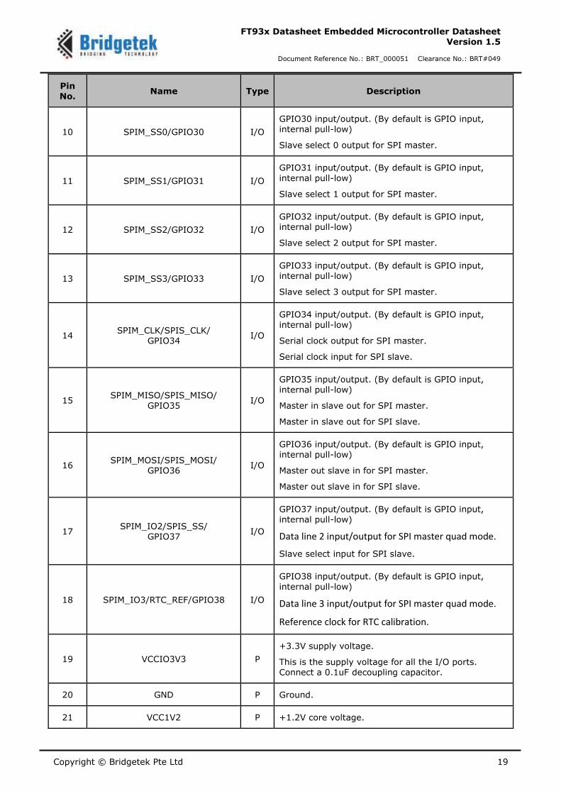
Pin No.
Name Type Description
10 SPIM_SS0/GPIO30 I/O
GPIO30 input/output. (By default is GPIO input, internal pull-low)
Slave select 0 output for SPI master.
11 SPIM_SS1/GPIO31 I/O
GPIO31 input/output. (By default is GPIO input,
internal pull-low)
Slave select 1 output for SPI master.
12 SPIM_SS2/GPIO32 I/O
GPIO32 input/output. (By default is GPIO input, internal pull-low)
Slave select 2 output for SPI master.
13 SPIM_SS3/GPIO33 I/O
GPIO33 input/output. (By default is GPIO input, internal pull-low)
Slave select 3 output for SPI master.
14 SPIM_CLK/SPIS_CLK/
GPIO34 I/O
GPIO34 input/output. (By default is GPIO input, internal pull-low)
Serial clock output for SPI master.
Serial clock input for SPI slave.
15 SPIM_MISO/SPIS_MISO/
GPIO35 I/O
GPIO35 input/output. (By default is GPIO input, internal pull-low)
Master in slave out for SPI master.
Master in slave out for SPI slave.
16 SPIM_MOSI/SPIS_MOSI/
GPIO36 I/O
GPIO36 input/output. (By default is GPIO input, internal pull-low)
Master out slave in for SPI master.
Master out slave in for SPI slave.
17 SPIM_IO2/SPIS_SS/
GPIO37 I/O
GPIO37 input/output. (By default is GPIO input, internal pull-low)
Data line 2 input/output for SPI master quad mode.
Slave select input for SPI slave.
18 SPIM_IO3/RTC_REF/GPIO38 I/O
GPIO38 input/output. (By default is GPIO input, internal pull-low)
Data line 3 input/output for SPI master quad mode.
Reference clock for RTC calibration.
19 VCCIO3V3 P
+3.3V supply voltage.
This is the supply voltage for all the I/O ports. Connect a 0.1uF decoupling capacitor.
20 GND P Ground.
21 VCC1V2 P +1.2V core voltage.
Copyright © Bridgetek Pte Ltd 20
FT93x Datasheet Embedded Microcontroller Datasheet Version 1.5
Document Reference No.: BRT_000051 Clearance No.: BRT#049
Pin No.
Name Type Description
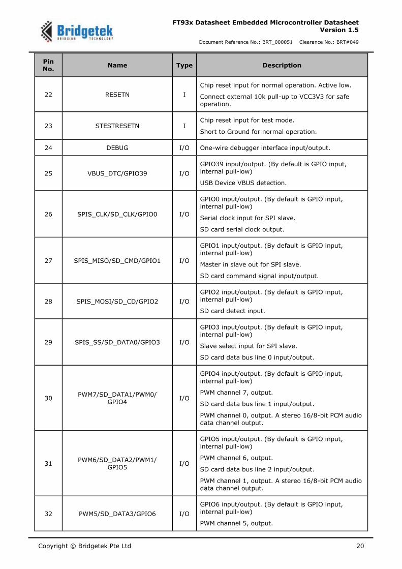
22 RESETN I
Chip reset input for normal operation. Active low.
Connect external 10k pull-up to VCC3V3 for safe operation.
23 STESTRESETN I Chip reset input for test mode.
Short to Ground for normal operation.
24 DEBUG I/O One-wire debugger interface input/output.
25 VBUS_DTC/GPIO39 I/O
GPIO39 input/output. (By default is GPIO input, internal pull-low)
USB Device VBUS detection.
26 SPIS_CLK/SD_CLK/GPIO0 I/O
GPIO0 input/output. (By default is GPIO input, internal pull-low)
Serial clock input for SPI slave.
SD card serial clock output.
27 SPIS_MISO/SD_CMD/GPIO1 I/O
GPIO1 input/output. (By default is GPIO input, internal pull-low)
Master in slave out for SPI slave.
SD card command signal input/output.
28 SPIS_MOSI/SD_CD/GPIO2 I/O
GPIO2 input/output. (By default is GPIO input, internal pull-low)
SD card detect input.
29 SPIS_SS/SD_DATA0/GPIO3 I/O
GPIO3 input/output. (By default is GPIO input, internal pull-low)
Slave select input for SPI slave.
SD card data bus line 0 input/output.
30 PWM7/SD_DATA1/PWM0/
GPIO4 I/O
GPIO4 input/output. (By default is GPIO input, internal pull-low)
PWM channel 7, output.
SD card data bus line 1 input/output.
PWM channel 0, output. A stereo 16/8-bit PCM audio
data channel output.
31 PWM6/SD_DATA2/PWM1/
GPIO5 I/O
GPIO5 input/output. (By default is GPIO input,
internal pull-low)
PWM channel 6, output.
SD card data bus line 2 input/output.
PWM channel 1, output. A stereo 16/8-bit PCM audio data channel output.
32 PWM5/SD_DATA3/GPIO6 I/O
GPIO6 input/output. (By default is GPIO input,
internal pull-low)
PWM channel 5, output.
Copyright © Bridgetek Pte Ltd 21
FT93x Datasheet Embedded Microcontroller Datasheet Version 1.5
Document Reference No.: BRT_000051 Clearance No.: BRT#049
Pin No.
Name Type Description
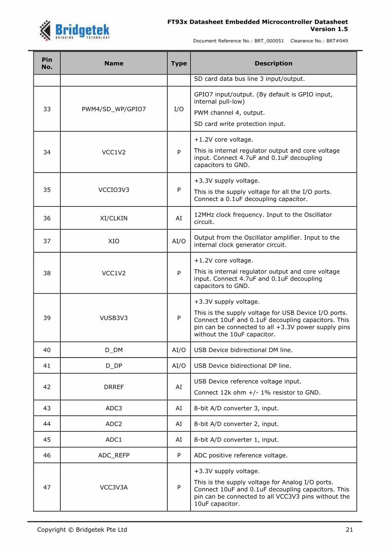
SD card data bus line 3 input/output.
33 PWM4/SD_WP/GPIO7 I/O
GPIO7 input/output. (By default is GPIO input, internal pull-low)
PWM channel 4, output.
SD card write protection input.
34 VCC1V2 P
+1.2V core voltage.
This is internal regulator output and core voltage input. Connect 4.7uF and 0.1uF decoupling capacitors to GND.
35 VCCIO3V3 P
+3.3V supply voltage.
This is the supply voltage for all the I/O ports. Connect a 0.1uF decoupling capacitor.
36 XI/CLKIN AI 12MHz clock frequency. Input to the Oscillator circuit.
37 XIO AI/O Output from the Oscillator amplifier. Input to the
internal clock generator circuit.
38 VCC1V2 P
+1.2V core voltage.
This is internal regulator output and core voltage input. Connect 4.7uF and 0.1uF decoupling capacitors to GND.
39 VUSB3V3 P
+3.3V supply voltage.
This is the supply voltage for USB Device I/O ports. Connect 10uF and 0.1uF decoupling capacitors. This pin can be connected to all +3.3V power supply pins
without the 10uF capacitor.
40 D_DM AI/O USB Device bidirectional DM line.
41 D_DP AI/O USB Device bidirectional DP line.
42 DRREF AI USB Device reference voltage input.
Connect 12k ohm +/- 1% resistor to GND.
43 ADC3 AI 8-bit A/D converter 3, input.
44 ADC2 AI 8-bit A/D converter 2, input.
45 ADC1 AI 8-bit A/D converter 1, input.
46 ADC_REFP P ADC positive reference voltage.
47 VCC3V3A P
+3.3V supply voltage.
This is the supply voltage for Analog I/O ports. Connect 10uF and 0.1uF decoupling capacitors. This pin can be connected to all VCC3V3 pins without the 10uF capacitor.
Copyright © Bridgetek Pte Ltd 22
FT93x Datasheet Embedded Microcontroller Datasheet Version 1.5
Document Reference No.: BRT_000051 Clearance No.: BRT#049
Pin No.
Name Type Description
48 AGND P Analog Ground.
49 DAC_REFP P DAC positive reference voltage.
50 DAC1 AO 10-bit D/A converter 1, output.
51 DAC0 AO 10-bit D/A converter 0, output.
52 RTC_XIO AO Output from the RTC Oscillator amplifier.
53 RTC_XI/RTC_CLKIN AI 32.768KHz clock frequency input to the RTC Oscillator circuit or to internal RTC clock generator circuit.
54 VDDBAT P +1.5V real time clock supply voltage.
55 I2CM_SCL/I2CS_SCL/
GPIO12 I/O
GPIO12 input/output. (By default is GPIO input, internal pull-low)
I2C master serial clock input/output.
I2C slave serial clock input/output.
56 I2CM_SDA/I2CS_SDA/
GPIO13 I/O
GPIO13 input/output. (By default is GPIO input, internal pull-low)
I2C master data line input/output.
I2C slave data line input/output.
Table 3-2 FT931 Pin Description

Copyright © Bridgetek Pte Ltd 23
FT93x Datasheet Embedded Microcontroller Datasheet Version 1.5
Document Reference No.: BRT_000051 Clearance No.: BRT#049
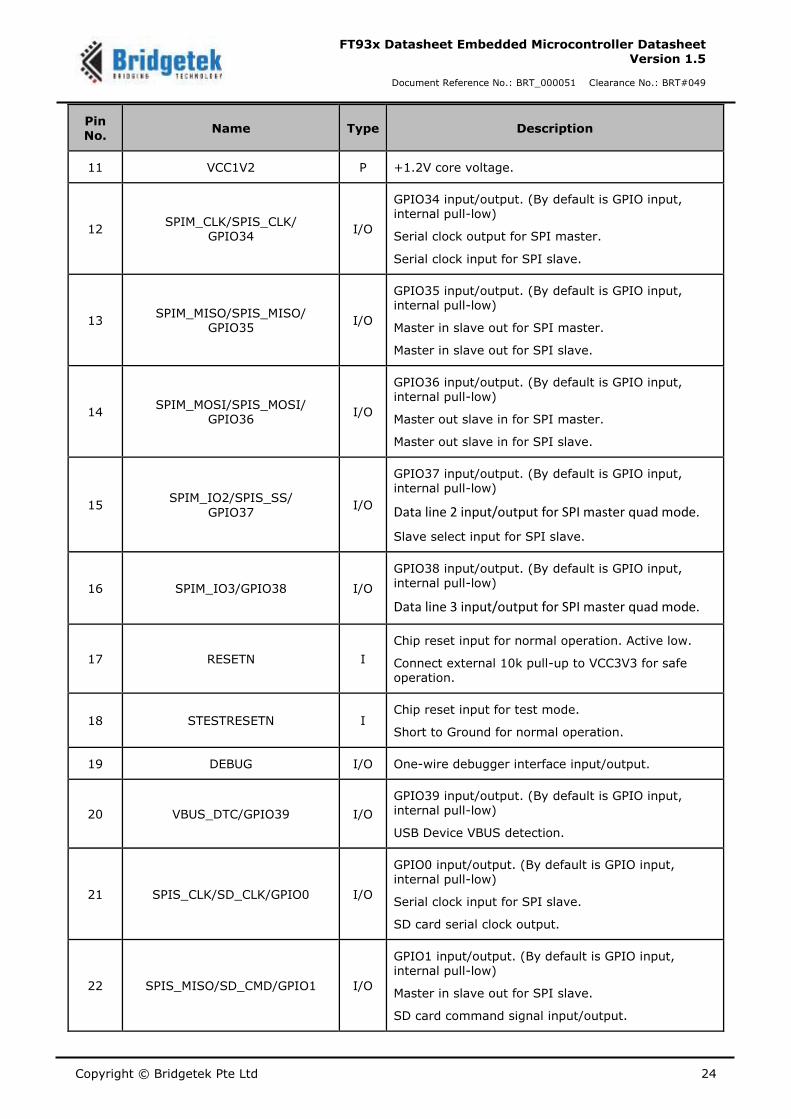
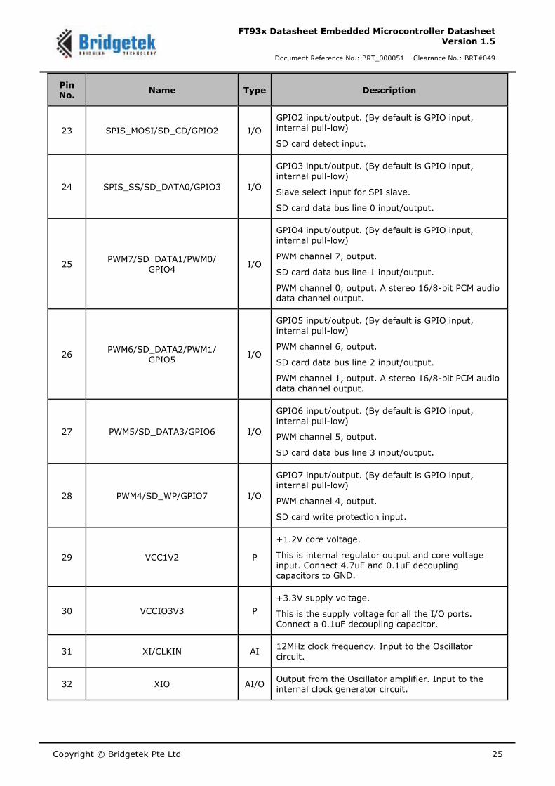
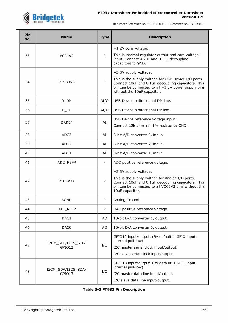
3.7 FT932 Pin Description
Pin
No. Name Type Description
1 UART0_RXD/PWM3/
GPIO22 I/O
GPIO22 input/output. (By default is GPIO input, internal pull-low)
Receiver input for UART0.
PWM channel 3, output.
2 UART0_TXD/PWM2/
GPIO23 I/O
GPIO23 input/output. (By default is GPIO input, internal pull-low)
Transmitter output for UART0.
PWM channel 2, output.
3 UART0_RTS/PWM1/
GPIO24 I/O
GPIO24 input/output. (By default is GPIO input, internal pull-low)
Request to send output for UART0.
PWM channel 1, output.
4 UART0_CTS/PWM0/
GPIO25 I/O
GPIO25 input/output. (By default is GPIO input, internal pull-low)
Clear to send input for UART0.
PWM channel 0, output.
5 UART0_DTR/UART1_RXD/
GPIO26 I/O
GPIO26 input/output. (By default is GPIO input, internal pull-low)
Data terminal ready output for UART0.
Receiver input for UART1.
6 UART0_DSR/UART1_TXD/
GPIO27 I/O
GPIO27 input/output. (By default is GPIO input, internal pull-low)
Data set ready input for UART0
Transmitter output for UART1.
7 UART0_DCD/UART1_RTS/
GPIO28 I/O
GPIO28 input/output. (By default is GPIO input, internal pull-low)
Data carrier detection input for UART0.
Request to send output for UART1.
8 UART0_RI/UART1_CTS/
SPIM_SS0/GPIO29 I/O
GPIO29 input/output. (By default is GPIO input, internal pull-low)
Ring indicator input for UART0.
Clear to send input for UART1.
Slave select 0 output for SPI master.
9 VCCIO3V3 P
+3.3V supply voltage.
This is the supply voltage for all the I/O ports. Connect a 0.1uF decoupling capacitor.
10 GND P Ground.
Copyright © Bridgetek Pte Ltd 24
FT93x Datasheet Embedded Microcontroller Datasheet Version 1.5
Document Reference No.: BRT_000051 Clearance No.: BRT#049
Pin No.
Name Type Description
11 VCC1V2 P +1.2V core voltage.
12 SPIM_CLK/SPIS_CLK/
GPIO34 I/O
GPIO34 input/output. (By default is GPIO input, internal pull-low)
Serial clock output for SPI master.
Serial clock input for SPI slave.
13 SPIM_MISO/SPIS_MISO/
GPIO35 I/O
GPIO35 input/output. (By default is GPIO input, internal pull-low)
Master in slave out for SPI master.
Master in slave out for SPI slave.
14 SPIM_MOSI/SPIS_MOSI/
GPIO36 I/O
GPIO36 input/output. (By default is GPIO input, internal pull-low)
Master out slave in for SPI master.
Master out slave in for SPI slave.
15 SPIM_IO2/SPIS_SS/
GPIO37 I/O
GPIO37 input/output. (By default is GPIO input, internal pull-low)
Data line 2 input/output for SPI master quad mode.
Slave select input for SPI slave.
16 SPIM_IO3/GPIO38 I/O
GPIO38 input/output. (By default is GPIO input, internal pull-low)
Data line 3 input/output for SPI master quad mode.
17 RESETN I
Chip reset input for normal operation. Active low.
Connect external 10k pull-up to VCC3V3 for safe operation.
18 STESTRESETN I Chip reset input for test mode.
Short to Ground for normal operation.
19 DEBUG I/O One-wire debugger interface input/output.
20 VBUS_DTC/GPIO39 I/O
GPIO39 input/output. (By default is GPIO input, internal pull-low)
USB Device VBUS detection.
21 SPIS_CLK/SD_CLK/GPIO0 I/O
GPIO0 input/output. (By default is GPIO input,
internal pull-low)
Serial clock input for SPI slave.
SD card serial clock output.
22 SPIS_MISO/SD_CMD/GPIO1 I/O
GPIO1 input/output. (By default is GPIO input, internal pull-low)
Master in slave out for SPI slave.
SD card command signal input/output.
Copyright © Bridgetek Pte Ltd 25
FT93x Datasheet Embedded Microcontroller Datasheet Version 1.5
Document Reference No.: BRT_000051 Clearance No.: BRT#049
Pin No.
Name Type Description
23 SPIS_MOSI/SD_CD/GPIO2 I/O
GPIO2 input/output. (By default is GPIO input, internal pull-low)
SD card detect input.
24 SPIS_SS/SD_DATA0/GPIO3 I/O
GPIO3 input/output. (By default is GPIO input,
internal pull-low)
Slave select input for SPI slave.
SD card data bus line 0 input/output.
25 PWM7/SD_DATA1/PWM0/
GPIO4 I/O
GPIO4 input/output. (By default is GPIO input, internal pull-low)
PWM channel 7, output.
SD card data bus line 1 input/output.
PWM channel 0, output. A stereo 16/8-bit PCM audio data channel output.
26 PWM6/SD_DATA2/PWM1/
GPIO5 I/O
GPIO5 input/output. (By default is GPIO input, internal pull-low)
PWM channel 6, output.
SD card data bus line 2 input/output.
PWM channel 1, output. A stereo 16/8-bit PCM audio data channel output.
27 PWM5/SD_DATA3/GPIO6 I/O
GPIO6 input/output. (By default is GPIO input, internal pull-low)
PWM channel 5, output.
SD card data bus line 3 input/output.
28 PWM4/SD_WP/GPIO7 I/O
GPIO7 input/output. (By default is GPIO input, internal pull-low)
PWM channel 4, output.
SD card write protection input.
29 VCC1V2 P
+1.2V core voltage.
This is internal regulator output and core voltage input. Connect 4.7uF and 0.1uF decoupling capacitors to GND.
30 VCCIO3V3 P
+3.3V supply voltage.
This is the supply voltage for all the I/O ports. Connect a 0.1uF decoupling capacitor.
31 XI/CLKIN AI 12MHz clock frequency. Input to the Oscillator
circuit.
32 XIO AI/O Output from the Oscillator amplifier. Input to the internal clock generator circuit.
Copyright © Bridgetek Pte Ltd 26
FT93x Datasheet Embedded Microcontroller Datasheet Version 1.5
Document Reference No.: BRT_000051 Clearance No.: BRT#049
Pin No.
Name Type Description
33 VCC1V2 P
+1.2V core voltage.
This is internal regulator output and core voltage input. Connect 4.7uF and 0.1uF decoupling capacitors to GND.
34 VUSB3V3 P
+3.3V supply voltage.
This is the supply voltage for USB Device I/O ports. Connect 10uF and 0.1uF decoupling capacitors. This pin can be connected to all +3.3V power supply pins without the 10uF capacitor.
35 D_DM AI/O USB Device bidirectional DM line.
36 D_DP AI/O USB Device bidirectional DP line.
37 DRREF AI USB Device reference voltage input.
Connect 12k ohm +/- 1% resistor to GND.
38 ADC3 AI 8-bit A/D converter 3, input.
39 ADC2 AI 8-bit A/D converter 2, input.
40 ADC1 AI 8-bit A/D converter 1, input.
41 ADC_REFP P ADC positive reference voltage.
42 VCC3V3A P
+3.3V supply voltage.
This is the supply voltage for Analog I/O ports.
Connect 10uF and 0.1uF decoupling capacitors. This
pin can be connected to all VCC3V3 pins without the 10uF capacitor.
43 AGND P Analog Ground.
44 DAC_REFP P DAC positive reference voltage.
45 DAC1 AO 10-bit D/A converter 1, output.
46 DAC0 AO 10-bit D/A converter 0, output.
47 I2CM_SCL/I2CS_SCL/
GPIO12 I/O
GPIO12 input/output. (By default is GPIO input, internal pull-low)
I2C master serial clock input/output.
I2C slave serial clock input/output.
48 I2CM_SDA/I2CS_SDA/
GPIO13 I/O
GPIO13 input/output. (By default is GPIO input, internal pull-low)
I2C master data line input/output.
I2C slave data line input/output.
Table 3-3 FT932 Pin Description

Copyright © Bridgetek Pte Ltd 27
FT93x Datasheet Embedded Microcontroller Datasheet Version 1.5
Document Reference No.: BRT_000051 Clearance No.: BRT#049
3.8 FT933 Pin Description
Pin
No. Name Type Description
1 UART0_RXD/PWM3/
GPIO22 I/O
GPIO22 input/output. (By default is GPIO input, internal pull-low)
Receiver input for UART0.
PWM channel 3, output.
2 UART0_TXD/PWM2/
GPIO23 I/O
GPIO23 input/output. (By default is GPIO input, internal pull-low)
Transmitter output for UART0.
PWM channel 2, output.
3 UART0_RTS/PWM1/
GPIO24 I/O
GPIO24 input/output. (By default is GPIO input, internal pull-low)
Request to send output for UART0.
PWM channel 1, output.
4 UART0_CTS/PWM0/
GPIO25 I/O
GPIO25 input/output. (By default is GPIO input, internal pull-low)
Clear to send input for UART0.
PWM channel 0, output.
5 UART0_DTR/UART1_RXD/
GPIO26 I/O
GPIO26 input/output. (By default is GPIO input, internal pull-low)
Data terminal ready output for UART0.
Receiver input for UART1.
6 UART0_DSR/UART1_TXD/
GPIO27 I/O
GPIO27 input/output. (By default is GPIO input, internal pull-low)
Data set ready input for UART0
Transmitter output for UART1.
7 UART0_DCD/UART1_RTS/
GPIO28 I/O
GPIO28 input/output. (By default is GPIO input, internal pull-low)
Data carrier detection input for UART0.
Request to send output for UART1.
8 UART0_RI/UART1_CTS/
SPIM_SS0/GPIO29 I/O
GPIO29 input/output. (By default is GPIO input, internal pull-low)
Ring indicator input for UART0.
Clear to send input for UART1.
Slave select 0 output for SPI master.
9 VCCIO3V3 P
+3.3V supply voltage.
This is the supply voltage for all the I/O ports. Connect a 0.1uF decoupling capacitor.
10 GND P Ground.
Copyright © Bridgetek Pte Ltd 28
FT93x Datasheet Embedded Microcontroller Datasheet Version 1.5
Document Reference No.: BRT_000051 Clearance No.: BRT#049
Pin No.
Name Type Description
11 VCC1V2 P +1.2V core voltage.
12 SPIM_CLK/SPIS_CLK/
GPIO34 I/O
GPIO34 input/output. (By default is GPIO input, internal pull-low)
Serial clock output for SPI master.
Serial clock input for SPI slave.
13 SPIM_MISO/SPIS_MISO/
GPIO35 I/O
GPIO35 input/output. (By default is GPIO input, internal pull-low)
Master in slave out for SPI master.
Master in slave out for SPI slave.
14 SPIM_MOSI/SPIS_MOSI/
GPIO36 I/O
GPIO36 input/output. (By default is GPIO input, internal pull-low)
Master out slave in for SPI master.
Master out slave in for SPI slave.
15 SPIM_IO2/SPIS_SS/
GPIO37 I/O
GPIO37 input/output. (By default is GPIO input, internal pull-low)
Data line 2 input/output for SPI master quad mode.
Slave select input for SPI slave.
16 SPIM_IO3/GPIO38 I/O
GPIO38 input/output. (By default is GPIO input, internal pull-low)
Data line 3 input/output for SPI master quad mode.
17 RESETN I
Chip reset input for normal operation. Active low.
Connect external 10k pull-up to VCC3V3 for safe operation.
18 STESTRESETN I Chip reset input for test mode.
Short to Ground for normal operation.
19 DEBUG I/O One-wire debugger interface input/output.
20 VBUS_DTC/GPIO39 I/O
GPIO39 input/output. (By default is GPIO input, internal pull-low)
USB Device VBUS detection.
21 NC - Not connected.
22 NC - Not connected.
23 NC - Not connected.
24 NC - Not connected.
25 NC - Not connected.
26 NC - Not connected.
Copyright © Bridgetek Pte Ltd 29
FT93x Datasheet Embedded Microcontroller Datasheet Version 1.5
Document Reference No.: BRT_000051 Clearance No.: BRT#049
Pin No.
Name Type Description
27 NC - Not connected.
28 NC - Not connected.
29 VCC1V2 P
+1.2V core voltage.
This is internal regulator output and core voltage input. Connect 4.7uF and 0.1uF decoupling capacitors to GND.
30 VCCIO3V3 P
+3.3V supply voltage.
This is the supply voltage for all the I/O ports. Connect a 0.1uF decoupling capacitor.
31 XI/CLKIN AI 12MHz clock frequency. Input to the Oscillator circuit.
32 XIO AI/O Output from the Oscillator amplifier. Input to the internal clock generator circuit.
33 VCC1V2 P
+1.2V core voltage.
This is internal regulator output and core voltage input. Connect 4.7uF and 0.1uF decoupling capacitors to GND.
34 VUSB3V3 P
+3.3V supply voltage.
This is the supply voltage for USB Device I/O ports. Connect 10uF and 0.1uF decoupling capacitors. This pin can be connected to all +3.3V power supply pins
without the 10uF capacitor.
35 D_DM AI/O USB Device bidirectional DM line.
36 D_DP AI/O USB Device bidirectional DP line.
37 DRREF AI USB Device reference voltage input.
Connect 12k ohm +/- 1% resistor to GND.
38 ADC3 AI 8-bit A/D converter 3, input.
39 ADC2 AI 8-bit A/D converter 2, input.
40 NC - Not connected.
41 ADC_REFP P ADC positive reference voltage.
42 VCC3V3A P
+3.3V supply voltage.
This is the supply voltage for Analog I/O ports. Connect 10uF and 0.1uF decoupling capacitors. This
pin can be connected to all VCC3V3 pins without the 10uF capacitor.
43 AGND P Analog Ground.
44 NC - Not connected.
Copyright © Bridgetek Pte Ltd 30
FT93x Datasheet Embedded Microcontroller Datasheet Version 1.5
Document Reference No.: BRT_000051 Clearance No.: BRT#049
Pin No.
Name Type Description
45 NC - Not connected.
46 NC - Not connected.
47 I2CM_SCL/I2CS_SCL/
GPIO12 I/O
GPIO12 input/output. (By default is GPIO input, internal pull-low)
I2C master serial clock input/output.
I2C slave serial clock input/output.
48 I2CM_SDA/I2CS_SDA/
GPIO13 I/O
GPIO13 input/output. (By default is GPIO input, internal pull-low)
I2C master data line input/output.
I2C slave data line input/output.
Table 3-4 FT933 Pin Description
Notes:
P : Power or Ground
I : Input
O : Output
OD : Open drain output
I/O : Bi-direction Input and Output
AI : Analog Input
AO : Analog Output
AI/O : Analog Input/output
Copyright © Bridgetek Pte Ltd 31
FT93x Datasheet Embedded Microcontroller Datasheet Version 1.5
Document Reference No.: BRT_000051 Clearance No.: BRT#049
4 Function Description
4.1 Architectural Overview
The FT93x series embedded microcontroller includes a high performance 32-bit FT32B RISC core processor and a D2XX hardware engine.
There is a 128KB high speed Flash memory for software program download with One-Wire debugger interface. The core processor uses a 32-bit I/O system bus to connect to all of the peripherals.
32-bit MCU Processor Core
D2XX hardware engine
128kB Flash Memory
128kB Program Memory
32kB Data RAM
USB2.0 Device Controller
- Control Endpoint 0 (8B to 64B)
- Data Endpoints 1 ~ 15 (8,128B)
BCD (Battery Charging Detection)
Real Time Clock
One-Wire debugger interface
One SPI Master interface
One SPI Slave interface or SD Host Controller
One I2C Master or one I2C Slave interface (3.4Mbps)
Four programmable 8Mbit/s UARTs
Four 16-bit timers and one 32-bit watchdog timer
8-Channel PWM with optional 2-Channel Audio PCM
10-bit two channel 1MS/s DAC
8-bit three channel 460KS/s ADC
General purpose I/O interface
The functions for each controller / interface are briefly described in the following subsections.
4.2 FT32B Core Processor
The FT32B core processor runs at frequencies of up to 100MHz. The processor contains the CPU itself with control logic and its 128kB program memory and 32kB data memory. The outside connections for the core processor are the memory-mapped I/O interface, the interrupt interface, asynchronous reset,
and the system clock.
4.3 D2XX Hardware Engine
The built-in D2XX hardware engine reduces the FT93x processor load of handling the USB protocol and
software complexity. When the D2XX hardware engine is enabled and takes over the control of the USB Device interface, the FT93x enumerates as a multiple interface, bi-directional D2XX USB Device which is
supported on most common platforms with a D2XX driver. The data transfer from the main processor to the USB is through the FT93x D2XX FIFO interface. It supports up to 7 FIFO channels, each corresponding to a D2XX interface.
Each channel has dedicated read and write pipes. There are a total of 14 pipes and 8,192B(8kB) of memory is reserved for the read and the write pipes. The maximum transfer size on a channel may be
flexibly allocated as 2 to 4094 bytes across the D2XX FIFO interfaces 1 to 7.
Copyright © Bridgetek Pte Ltd 32
FT93x Datasheet Embedded Microcontroller Datasheet Version 1.5
Document Reference No.: BRT_000051 Clearance No.: BRT#049
4.4 128kB Flash Memory
The internal 128kB Flash memory is used to store a bootloader or user application for the FT93x series. It is a high performance and low power consumption memory that supports up to 80MHz serial clock. The system will perform memory copy from Flash memory to CPU program memory automatically after
system power on.
4.5 Boot Sequence
After the initial memory copy completes, the CPU jumps to program memory location zero. This may be the start of the user’s application which is stored in advance in the flash memory, or a bootloader, which allows modification of the program memory via UART or USB as an example.
The option of a bootloader is a special purpose routine in the FT93x Series embedded microcontroller. It is a small routine stored in the flash memory. Typically, the bootloader is 1kB to 4kB in size, and resides at the top of the memory.
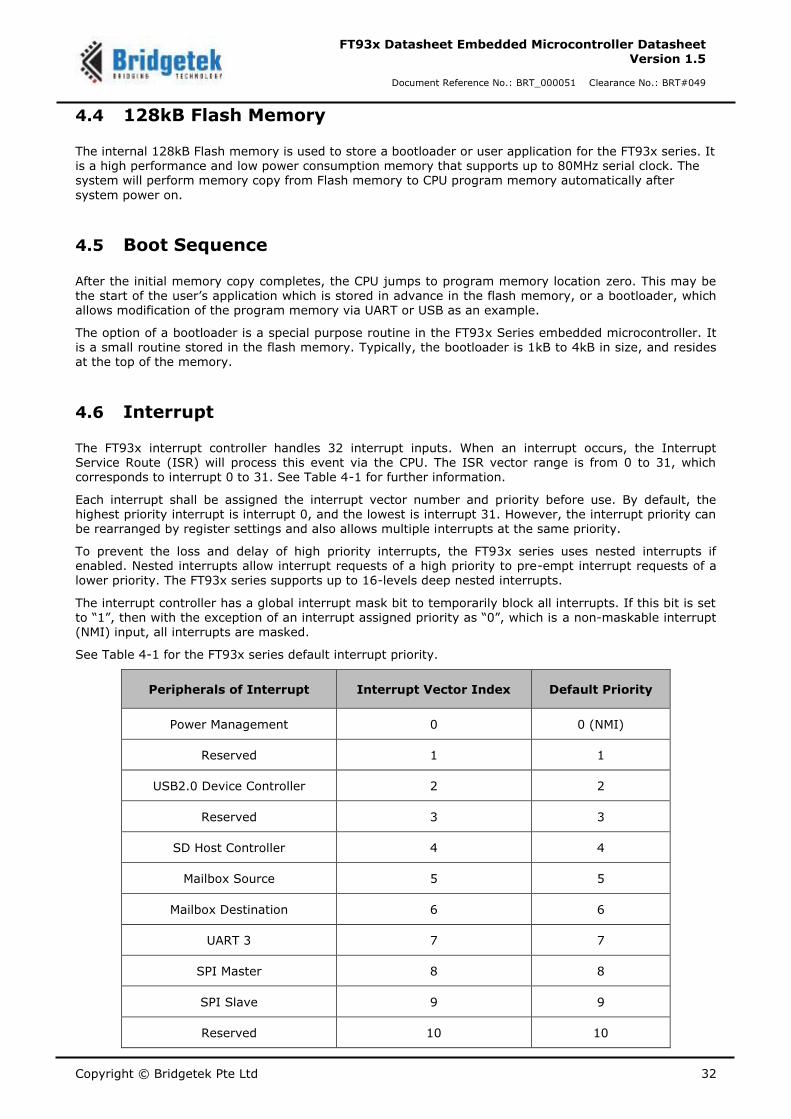
4.6 Interrupt
The FT93x interrupt controller handles 32 interrupt inputs. When an interrupt occurs, the Interrupt Service Route (ISR) will process this event via the CPU. The ISR vector range is from 0 to 31, which corresponds to interrupt 0 to 31. See Table 4-1 for further information.
Each interrupt shall be assigned the interrupt vector number and priority before use. By default, the highest priority interrupt is interrupt 0, and the lowest is interrupt 31. However, the interrupt priority can be rearranged by register settings and also allows multiple interrupts at the same priority.
To prevent the loss and delay of high priority interrupts, the FT93x series uses nested interrupts if enabled. Nested interrupts allow interrupt requests of a high priority to pre-empt interrupt requests of a lower priority. The FT93x series supports up to 16-levels deep nested interrupts.
The interrupt controller has a global interrupt mask bit to temporarily block all interrupts. If this bit is set to “1”, then with the exception of an interrupt assigned priority as “0”, which is a non-maskable interrupt
(NMI) input, all interrupts are masked.
See Table 4-1 for the FT93x series default interrupt priority.
Peripherals of Interrupt Interrupt Vector Index Default Priority
Power Management 0 0 (NMI)
Reserved 1 1
USB2.0 Device Controller 2 2
Reserved 3 3
SD Host Controller 4 4
Mailbox Source 5 5
Mailbox Destination 6 6
UART 3 7 7
SPI Master 8 8
SPI Slave 9 9
Reserved 10 10
Copyright © Bridgetek Pte Ltd 33
FT93x Datasheet Embedded Microcontroller Datasheet Version 1.5
Document Reference No.: BRT_000051 Clearance No.: BRT#049
Peripherals of Interrupt Interrupt Vector Index Default Priority
I2C Master 11 11
I2C Slave 12 12
UART 0 13 13
UART 1 14 14
UART 2 15 15
PWM 16 16
Timers 17 17
GPIO 18 18
RTC 19 19
ADC 20 20
DAC 21 21
Slow Clock Timer 22 22
UNUSED 24-31 24-31
Table 4-1 FT93x Series Default Interrupt Priority
4.7 Memory Mapping
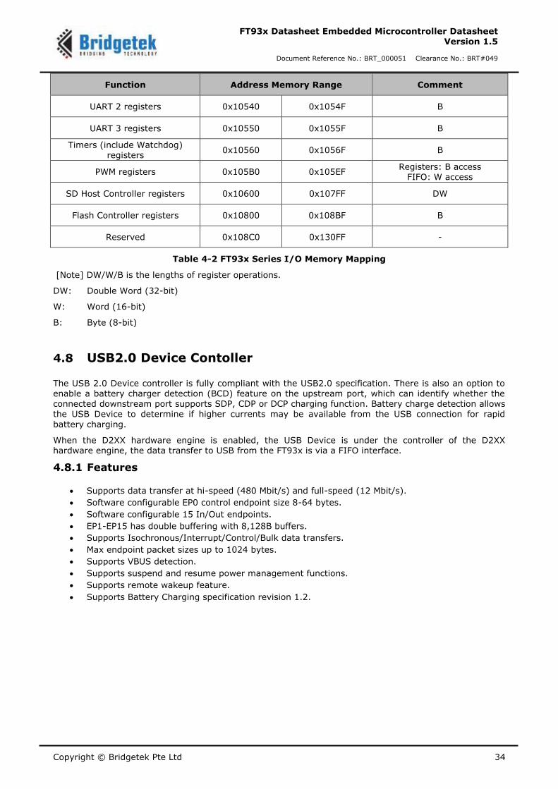
A list of the I/O memory mapping for registers and memory in the FT93x series is given below in Table 4-2. Refer to the FT93x User Manual for a detailed description of the registers.
Function Address Memory Range Comment
General Setup registers 0x10000 0x100FF DW/W/B
Interrupt controller registers 0x10100 0x1013F DW/W/B
USB2.0 Device Controller registers
0x10200 0x1031F DW/W/B
RTC registers 0x10400 0x1043F DW
SPI Master registers 0x10440 0x1047F DW
SPI Slave registers 0x10480 0x104BF DW
I2C Master registers 0x10500 0x1050F B
I2C Slave registers 0x10510 0x1051F B
UART 0 registers 0x10520 0x1052F B
UART 1 registers 0x10530 0x1053F B
Copyright © Bridgetek Pte Ltd 34
FT93x Datasheet Embedded Microcontroller Datasheet Version 1.5
Document Reference No.: BRT_000051 Clearance No.: BRT#049
Function Address Memory Range Comment
UART 2 registers 0x10540 0x1054F B
UART 3 registers 0x10550 0x1055F B
Timers (include Watchdog) registers
0x10560 0x1056F B
PWM registers 0x105B0 0x105EF Registers: B access
FIFO: W access
SD Host Controller registers 0x10600 0x107FF DW
Flash Controller registers 0x10800 0x108BF B
Reserved 0x108C0 0x130FF -
Table 4-2 FT93x Series I/O Memory Mapping
[Note] DW/W/B is the lengths of register operations.
DW: Double Word (32-bit)
W: Word (16-bit)
B: Byte (8-bit)
4.8 USB2.0 Device Contoller
The USB 2.0 Device controller is fully compliant with the USB2.0 specification. There is also an option to enable a battery charger detection (BCD) feature on the upstream port, which can identify whether the connected downstream port supports SDP, CDP or DCP charging function. Battery charge detection allows the USB Device to determine if higher currents may be available from the USB connection for rapid
battery charging.
When the D2XX hardware engine is enabled, the USB Device is under the controller of the D2XX hardware engine, the data transfer to USB from the FT93x is via a FIFO interface.
4.8.1 Features
Supports data transfer at hi-speed (480 Mbit/s) and full-speed (12 Mbit/s).
Software configurable EP0 control endpoint size 8-64 bytes.
Software configurable 15 In/Out endpoints.
EP1-EP15 has double buffering with 8,128B buffers.
Supports Isochronous/Interrupt/Control/Bulk data transfers.
Max endpoint packet sizes up to 1024 bytes.
Supports VBUS detection.
Supports suspend and resume power management functions.
Supports remote wakeup feature.
Supports Battery Charging specification revision 1.2.
Copyright © Bridgetek Pte Ltd 35
FT93x Datasheet Embedded Microcontroller Datasheet Version 1.5
Document Reference No.: BRT_000051 Clearance No.: BRT#049
4.9 Real Time Clock
The Real Time Clock (RTC) runs off a dedicated 32 kHz oscillator with its own power rail which can be connected to a separate battery.
4.9.1 Features
Two clock sources, PCLK and CLK32KHZ
Built-in Clock Stabilizer for CLK32KHZ
Records system sleep time
Supports Date and Time format in BCD
Counts Second, Minute, Hour, Day, Date of the Month, Month and Year with Leap-Year
Compensation Valid up to 2199
Supports two configurable Time-of-Day Alarms
Supports 1Hz and 32768Hz clock outputs
Supports interrupt with 4 configurable events
Supports Oscillator Stop Flag with both external trigger and internal auto detection
Supports On-Chip Digital Trimming with Auto Calibration
4.10 One-Wire Debugger Interface
The Debugger interface provides the capability over a One-Wire half duplex serial link, to access memory mapped address space, such as the FT93x flash memory, program memory, data memory, and I/O memory. However, there is no transfer capability from any of the internal memory to the debugger interface.
4.10.1 Features
Single wire half duplex link that has one Start, eight Data and one Stop bit at a 1M bit/s rate.
Supports debugger command read / write operation with variable data transfer.
Supports CHIP ID read out.
Supports checksum check by Flash memory operation.
Supports CPU software debugging to execute Run, Stop, Step, Halt, Set software breakpoint, etc.
operations.
Use semaphore flag to control resource allocated by CPU or Debugger.
4.11 SPI Interface
The FT93x series contains both SPI Master and SPI Slave controllers. SPI is a full duplex serial interface designed to handle multiple masters and slaves connected to a given bus.
4.11.1 Features
Maximum SPI data bit rate 25MHz in master and slave modes.
Full duplex synchronous serial data transfer.
Compliant with SPI specification, supporting four transfer formats.
SPI master supports Single, Dual, and Quad SPI transfer.
SPI Slave support Single transfer only.
Support SPI mode and FIFO mode operations.
Multi-master system supported.
Support bus error detection.
SPI master can address up to 4 SPI slave devices.
Support 64 Bytes receiver and 64 Bytes transmitter FIFO respectively.
Copyright © Bridgetek Pte Ltd 36
FT93x Datasheet Embedded Microcontroller Datasheet Version 1.5
Document Reference No.: BRT_000051 Clearance No.: BRT#049
4.12 I2C Interface
The FT93x series supports an I2C bus controller which is a bidirectional two wire interface. The two wires are Serial Clock line (SCL) and Serial Data line (SDA). The interface can be programed to operate with arbitration and clock synchronization allowing it to operate in multi-master systems. The I2C interface
supports transmission speeds up to 3.4Mb/s.
4.12.1 Features
Conforms to v2.1 and v3.0 of the I2C specification.
UM10204 I2C-bus specification and user manual Rev. 6 – 4 April 2014
Support flexible transmission speed modes:
- Standard (up to 100 kb/s)
- Fast (up to 400 kb/s)
- Fast-plus (up to 1 Mb/s)
- High-speed (up to 3.4 Mb/s)
The I2C interface can be configured to operate in Master mode or Slave mode.
Perform arbitration and clock synchronization.
Multi-master systems supported.
Support both 7-bit and 10-bit addressing modes on the I2C bus.
Support clock stretching.
4.13 UART Interface
The FT93x series contains four UART controllers with standard transmit and receive data lines. UART0 provides a full modem control handshake interface and support for 9-bit data, allowing automatic address detection while 9-bit data mode is enabled.
UART1 is a simplified programmable serial interface with CTS and RTS flow control logic. The signals are multiplexed with UART0 and can only be used if UART0 is used in simple mode (CTS/RTS only).
4.13.1 Features
Maximum UART data bit rate of 8 Mbit/s.
Two modes of operation : UART mode and FIFO mode
16 / 128 bytes FIFO for TX and RX in FIFO mode to reduce the interrupt frequency
Software compatible with 16450, 16550, 16750 and 16950 UARTs
MODEM control functions (CTS, RTS, DSR, DTR, RI and DCD)
Programmable automatic out-of-band Flow Control logic through Auto-RTS and Auto-CTS
Programmable automatic Flow Control logic using DTR and DSR
Programmable automatic in-band Flow Control logic using XON / XOFF characters
RS-485 buffer enable signals.
Fully programmable serial interface characteristics:
- 5-, 6-, 7-, 8- or 9-bit characters
- Even, odd, or no-parity bit generation and detection
- 1, 1.5, or 2 stop-bit generation
- Baud generation
- Detection of bad data in receive FIFO
Support Transmitter and Receiver disable capability.
4.14 Timers and Watchdog Timer
The FT93x series has four 16-bit user timers with individual prescaler and a 32-bit watchdog feature.
The watchdog timer is controlled from the main clock. The watchdog can be initialized with a 5-bit register. The value of this register points to a bit of the 32-bit counter which will be set by the application firmware.
Copyright © Bridgetek Pte Ltd 37
FT93x Datasheet Embedded Microcontroller Datasheet Version 1.5
Document Reference No.: BRT_000051 Clearance No.: BRT#049
As the timer decrements, an interrupt occurs when the timer rolls over. Once started and initialized the
watchdog can’t be stopped. It can only be cleared by writing into a register.
The four user timers can be controlled from the main clock, each timer has its own 16-bit prescaler. These timers can be started, stopped and cleared / initialized. The prescalers can be cleared/initialised the same way.
The current value of all timers/prescalers can be read from a common register one-at-a-time
(multiplexed access).
All timers can count up/down and signal an interrupt when the timer rolls over. The timers can also be configured to be one-shot or in continuous mode. They are initialised from a common register one-at-a-time (multiplexed access).
If the user timer has already started using its prescaler it cannot be cleared and the command is ignored. Each of the prescalers automatically stops after it is cleared individually. It also starts automatically when the corresponding user timer starts using it.
4.14.1 Features
Four user timers with individual prescaler.
Supports 16-bit prescaler with system clock reference.
Supports individual timer interrupt generation.
Supports one-shot and continuous count for timer.
Supports 32-bit counter watchdog.
Supports watchdog interrupt generation.
4.15 PWM
The FT93x series supports 8 separate independent PWM output channels. All channels share an 8-bit prescaler to scale the system clock frequency to the desired channels.
Each channel has its own 16-bit comparator value. This is the value that would be matched to a preset 16-bit counter. When a channel’s 16-bit comparator value matches that of the 16-bit counter, the corresponding PWM channel output will toggle. This 16-bit comparator value will continue to count until it
reaches its preset value, and the counter will just roll over.
A special feature allows each of the 8 channels to toggle its own output based on the comparison results of the other channels. Hence each channel potentially can have up to 8 toggle edges.
The PWM signal generated can be output as either multi-single-shot or continuous.
PWM channel 0 and channel 1 can double as a stereo 11 KHz or 22 KHz PWM audio channel.
Once this feature is setup, the 16-bit or 8-bit PCM audio data can be downloaded to the PWM local FIFO which can hold up to 64 bytes stereo or 128 bytes mono audio data. The data will be played back based
on the pre-scaler and 16-bit counter. The data will be automatically scaled to fit in the playback period if necessary.
The PWM FIFO can generate a number of interrupts for FIFO management. They are FIFO empty, full, half-full, overflow, and underflow.
Each of these interrupts can be individually masked if required.
4.15.1 Features
Support 8 PWM output channels.
Support multi-single-shot or continuous PWM data output.
Support external GPIO trigger.
Support 16-bit / 8-bit stereo PWM audio data output.
Control PWM FIFO full, empty, half-empty, overflow and underflow buffer management.
Support PCM volume control for audio playback.
Copyright © Bridgetek Pte Ltd 38
FT93x Datasheet Embedded Microcontroller Datasheet Version 1.5
Document Reference No.: BRT_000051 Clearance No.: BRT#049
4.16 SD Host Controller
The FT93x series contains one SD Host controller offering access to external large capacity non-volatile memory.
4.16.1 Features
Compliant with SD Host controller standard specification, version 3.0.
Supports both streaming and non-streaming data transfers.
Compliant with SD physical layer specification, version 3.0.
Supports configurable SD bus modes: 4-bit mode and 8-bit mode.
Compliant with SDIO card specification, version 2.0.
Support 4K SRAM for data FIFO.
Supports configurable 1-bit/4-bit SD card bus.
Configurable CPRM function for security.
Built-in generation and check for 7-bit and 16-bit CRC data.
Card detection (Insertion/Removal).
Supports read wait mechanism for SDIO function.
Supports suspend/resume mechanism for SDIO function.
4.17 Analog to Digital Converter (ADC)
The FT93x series has a low-power, high-speed, successive approximation Analog-to-Digital Converter (ADC) that supports 8-bit resolution and maximum sampling frequency up to 460kSPS.
This ADC accepts analog inputs ranging from the ground supply to the power supply. This ADC can be used in various low-power and medium-resolution applications.
4.17.1 Features
8-bit successive approximation ADC.
Three-channel analog input ADC1/2/3.
Individual channels can be selected for conversion.
Power-down mode support.
Maximum conversion rate of up to 460kSPS.
Measurement range 0 to VCC3V3A, by default the range voltage is 10% off of VCC3V3A. See
Table 5-7.
INL: +/-1LSB (max).
DNL: +/-1LSB (max).
4.18 Digital to Analog Converter (DAC)
The FT93x series has two 10-bit, 1 MSPS Digital-to-Analog converter (DAC). It includes digital logic for
registering the DAC value and a unity-gain buffer capable of driving off-chip. The module can also be switched to a power-down state where it consumes a minimum amount of current.
4.18.1 Features
Two 10-bit DACs (DAC0/1).
10-bit R2R DAC ladder structure.
Buffered output.
Power-down mode support.
Programmable conversion rate, the maximum rate is 1MHz.
Selectable output drive.
INL: +/-1.5LSB (max).
DNL: +/-1LSB (max).
Copyright © Bridgetek Pte Ltd 39
FT93x Datasheet Embedded Microcontroller Datasheet Version 1.5
Document Reference No.: BRT_000051 Clearance No.: BRT#049
4.19 General Purpose Input Output
The FT93x series provides up to 40 configurable Input/output pins controlled by GPIO registers. All pins
have multiple functions with special peripheral connection. Separate registers allow setting or clearing any number of outputs simultaneously.
All GPIO pins default to inputs with pull-down resistors enabled on reset.
All GPIOs can function as an interrupt. The polarity can be either positive edge or negative edge if the interrupt capability is enabled. In this case, the GPIO pin must be configured as a GPIO input.
4.19.1 Features
All GPIO default to inputs after reset.
Multi-function selection on GPIO pins.
Pull-up/Pull-down resistor configuration and open-drain configuration can be programmed
through the pin connect block for each GPIO pin.
Direction control of individual bits.
Supports GPIO input Schmitt trigger to help remove noise.
Supports GPIO interrupt, where each enabled GPIO interrupt can be used to wake-up the system from power-down mode.
4.20 System Clocks
4.20.1 12MHz Oscillator
The oscillator generates a 12MHz reference frequency output to the clock multiplier PLL. The oscillator clock source comes from either an external 12MHz crystal or a 12MHz square wave clock. The external crystal is connected across XI/CLKIN and XIO in the configuration shown in Section 6.1. The optional
external clock input is connected to XI only.
4.20.2 Phase Locked Loop
The internal PLL takes the 12MHz clock input from the crystal oscillator. The PLL outputs the 100MHz system clock frequency to the CPU processor and other peripheral circuits. Each peripheral has an individual enable control signal to gate the clock source.
4.20.3 32.768 kHz RTC Oscillator
The RTC oscillator provides a clock to the RTC time counter. An external 32.768 kHz crystal or a 32.768 kHz square wave signal can be used as the clock source.
The external crystal is connected across RTC_XI/RTC_CLKIN and RTC_XIO in the configuration shown in Section 6.2. The optional external clock input is connected to RTC_XI/RTC_CLKIN only.
4.20.4 Internal Slow Clock Oscillator
The internal slow clock oscillator provides a 5ms slow clock source to generate an interrupt for the USB2.0 device remote wake-up feature.
A USB2.0 device with remote wake-up capability may not generate a resume signal unless the bus has been continuously in the idle state for 5ms. For detailed description of the USB2.0 resume/suspend, refer to USB2.0 specification Chapters 7.1.7.6 & 7.1.7.7.
Copyright © Bridgetek Pte Ltd 40
FT93x Datasheet Embedded Microcontroller Datasheet Version 1.5
Document Reference No.: BRT_000051 Clearance No.: BRT#049
4.21 Power Management
4.21.1 Power Supply
The FT93x series may be operated with a single supply of +3.3V applied to VCCIO3V3, VUSB3V3, and VCC3V3A pins. The +1.2V internal regulator provides power to the core circuit after VCCIO3V3 power is
applied and the system will generate a Power on Reset (POR) pulse when the output voltage rises above the POR threshold.
4.21.2 Power down Mode
Power down mode applies to the entire system. In the power down mode, the system 12MHz oscillator and PLL both switch off and the system clock to the core and all peripherals stop except for the RTC
oscillator and internal regulator. The internal regulator retains power for the core and RTC operation.
An interrupt from GPIO or wake-up events from the USB2.0 Device controller can wake-up the system
from the power down mode independently.
If the USB2.0 Device controller was used and the respective interrupt bit was also enabled before the system entered into power down mode, then the following events can wake-up the system.
USB2.0 Device controller detects connects interrupt. USB2.0 Device controller detects disconnects interrupt.
USB Host issue reset signal to the USB2.0 Device controller. USB Host issue resume signal to the USB2.0 Device controller.
Copyright © Bridgetek Pte Ltd 41
FT93x Datasheet Embedded Microcontroller Datasheet Version 1.5
Document Reference No.: BRT_000051 Clearance No.: BRT#049
5 Device Characteristics and Ratings
5.1 Absolute Maximum Ratings
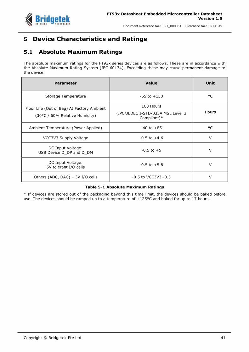
The absolute maximum ratings for the FT93x series devices are as follows. These are in accordance with the Absolute Maximum Rating System (IEC 60134). Exceeding these may cause permanent damage to the device.
Parameter Value Unit
Storage Temperature -65 to +150 °C
Floor Life (Out of Bag) At Factory Ambient
(30°C / 60% Relative Humidity)
168 Hours
(IPC/JEDEC J-STD-033A MSL Level 3
Compliant)*
Hours
Ambient Temperature (Power Applied) -40 to +85 °C
VCC3V3 Supply Voltage -0.5 to +4.6 V
DC Input Voltage: USB Device D_DP and D_DM
-0.5 to +5 V
DC Input Voltage: 5V tolerant I/O cells
-0.5 to +5.8 V
Others (ADC, DAC) – 3V I/O cells -0.5 to VCC3V3+0.5 V
Table 5-1 Absolute Maximum Ratings
* If devices are stored out of the packaging beyond this time limit, the devices should be baked before
use. The devices should be ramped up to a temperature of +125°C and baked for up to 17 hours.
Copyright © Bridgetek Pte Ltd 42
FT93x Datasheet Embedded Microcontroller Datasheet Version 1.5
Document Reference No.: BRT_000051 Clearance No.: BRT#049
5.2 DC Characteristics
Electrical Characteristics (Ambient Temperature = -40°C to +85°C)
The typical values are obtained at room temperature (Tj = 25°C), VCC3V3 = 3.3V, and VCC1V2 = 1.2V.
Parameter Description Minimum Typical Maximum Units Conditions
VCCIO3V3 I/O operating supply
voltage 2.97 3.3 3.63 V
Normal Operation
Icc1 Power down current - 780 - uA Power Down
Mode
Icc2 Idle current - 43 - mA Idle
Icc3
System operating current*
- 75 - mA
USB2.0 Device
controller high speed transfer
data
- 48 - mA ADC / DAC Operation
IOL/OH High level/Low level
total maximum output current
- - 96 mA For all GPIOs
VCC1V2 Internal LDO voltage - 1.2 - V Normal
Operation
Table 5-2 Operating Voltage and Current
Note*: The system operating typical current measured based on each function implements normal operation with FT32B core active, and other peripherals keep idle status.
DC characteristics of I/O cells
Parameter Description Minimum Typical Maximum Units Conditions
Voh Output Voltage
High 2.4 - - V
|Ioh|=2mA~16mA
Vol Output Voltage
Low - - 0.4 V |Iol|=2mA~16mA
Vopu*
Output pull-up
Voltage for 5V tolerance I/Os
VCCIO3V3-0.9
- - V |Ipu| = 1uA
Vih Input High Voltage 2.0 - - V LVTTL
Vil Input Low Voltage - - 0.8 V LVTTL
Vth Schmitt trigger
positive threshold Voltage
- 1.6 2.0 V LVTTL
Copyright © Bridgetek Pte Ltd 43
FT93x Datasheet Embedded Microcontroller Datasheet Version 1.5
Document Reference No.: BRT_000051 Clearance No.: BRT#049
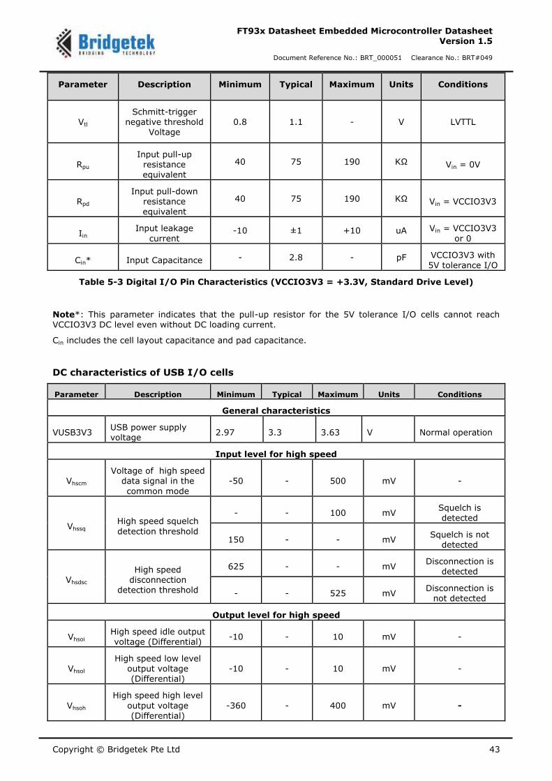
Parameter Description Minimum Typical Maximum Units Conditions
Vtl Schmitt-trigger
negative threshold Voltage
0.8 1.1 - V LVTTL
Rpu Input pull-up
resistance equivalent
40 75 190 KΩ Vin = 0V
Rpd Input pull-down
resistance equivalent
40 75 190 KΩ Vin = VCCIO3V3
Iin Input leakage
current -10 ±1 +10 uA Vin = VCCIO3V3
or 0
Cin* Input Capacitance - 2.8 - pF VCCIO3V3 with
5V tolerance I/O
Table 5-3 Digital I/O Pin Characteristics (VCCIO3V3 = +3.3V, Standard Drive Level)
Note*: This parameter indicates that the pull-up resistor for the 5V tolerance I/O cells cannot reach VCCIO3V3 DC level even without DC loading current.
Cin includes the cell layout capacitance and pad capacitance.
DC characteristics of USB I/O cells
Parameter Description Minimum Typical Maximum Units Conditions
General characteristics
VUSB3V3 USB power supply
voltage 2.97 3.3 3.63 V Normal operation
Input level for high speed
Vhscm Voltage of high speed
data signal in the
common mode
-50 - 500 mV -
Vhssq High speed squelch
detection threshold
- - 100 mV Squelch is detected
150 - - mV Squelch is not
detected
Vhsdsc High speed
disconnection detection threshold
625 - - mV Disconnection is
detected
- - 525 mV Disconnection is
not detected
Output level for high speed
Vhsoi High speed idle output voltage (Differential)
-10 - 10 mV -
Vhsol High speed low level
output voltage (Differential)
-10 - 10 mV -
Vhsoh
High speed high level
output voltage (Differential)
-360 - 400 mV -
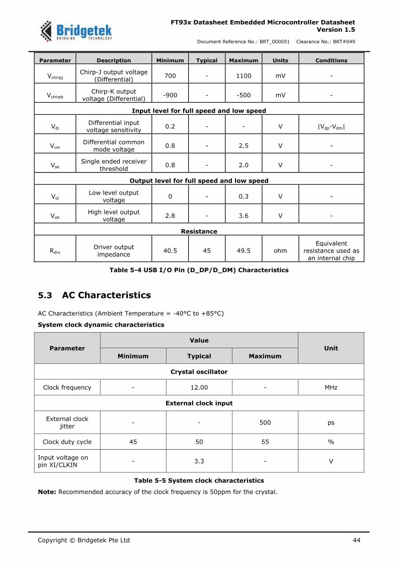
Copyright © Bridgetek Pte Ltd 44
FT93x Datasheet Embedded Microcontroller Datasheet Version 1.5
Document Reference No.: BRT_000051 Clearance No.: BRT#049
Parameter Description Minimum Typical Maximum Units Conditions
Vchirpj Chirp-J output voltage
(Differential) 700 - 1100 mV -
Vchirpk Chirp-K output
voltage (Differential) -900 - -500 mV -
Input level for full speed and low speed
Vdi Differential input voltage sensitivity
0.2 - - V |Vdp-Vdm|
Vcm Differential common
mode voltage 0.8 - 2.5 V -
Vse Single ended receiver
threshold 0.8 - 2.0 V -
Output level for full speed and low speed
Vol Low level output
voltage 0 - 0.3 V -
Voh High level output
voltage 2.8 - 3.6 V -
Resistance
Rdrv Driver output impedance
40.5 45 49.5 ohm Equivalent
resistance used as
an internal chip
Table 5-4 USB I/O Pin (D_DP/D_DM) Characteristics
5.3 AC Characteristics
AC Characteristics (Ambient Temperature = -40°C to +85°C)
System clock dynamic characteristics
Parameter
Value
Unit
Minimum Typical Maximum
Crystal oscillator
Clock frequency - 12.00 - MHz
External clock input
External clock jitter
- - 500 ps
Clock duty cycle 45 50 55 %
Input voltage on pin XI/CLKIN
- 3.3 - V
Table 5-5 System clock characteristics
Note: Recommended accuracy of the clock frequency is 50ppm for the crystal.
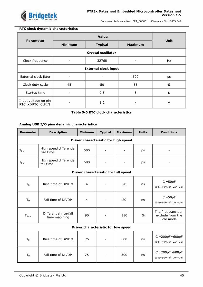
Copyright © Bridgetek Pte Ltd 45
FT93x Datasheet Embedded Microcontroller Datasheet Version 1.5
Document Reference No.: BRT_000051 Clearance No.: BRT#049
RTC clock dynamic characteristics
Parameter
Value
Unit
Minimum Typical Maximum
Crystal oscillator
Clock frequency - 32768 - Hz
External clock input
External clock jitter - - 500 ps
Clock duty cycle 45 50 55 %
Startup time - 0.5 5 s
Input voltage on pin RTC_XI/RTC_CLKIN
- 1.2 - V
Table 5-6 RTC clock characteristics
Analog USB I/O pins dynamic characteristics
Parameter Description Minimum Typical Maximum Units Conditions
Driver characteristic for high speed
Thsr High speed differential rise time
500 - - ps -
Thsf High speed differential fall time
500 - - ps -
Driver characteristic for full speed
Tfr Rise time of DP/DM 4 - 20 ns Cl=50pF
10%~90% of |Voh–Vol|
Tff Fall time of DP/DM 4 - 20 ns Cl=50pF
10%~90% of |Voh–Vol|
Tfrma Differential rise/fall
time matching 90 - 110 %
The first transition exclude from the
idle mode
Driver characteristic for low speed
Tlr Rise time of DP/DM 75 - 300 ns Cl=200pF~600pF
10%~90% of |Voh–Vol|
Tlf Fall time of DP/DM 75 - 300 ns Cl=200pF~600pF
10%~90% of |Voh–Vol|
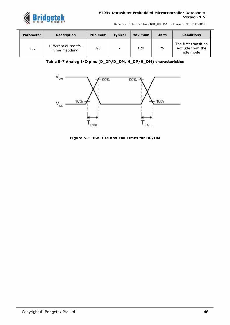
Copyright © Bridgetek Pte Ltd 46
FT93x Datasheet Embedded Microcontroller Datasheet Version 1.5
Document Reference No.: BRT_000051 Clearance No.: BRT#049
Parameter Description Minimum Typical Maximum Units Conditions
Tlrma Differential rise/fall
time matching 80 - 120 %
The first transition
exclude from the idle mode
Table 5-7 Analog I/O pins (D_DP/D_DM, H_DP/H_DM) characteristics
Figure 5-1 USB Rise and Fall Times for DP/DM
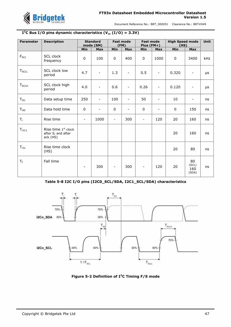
Copyright © Bridgetek Pte Ltd 47
FT93x Datasheet Embedded Microcontroller Datasheet Version 1.5
Document Reference No.: BRT_000051 Clearance No.: BRT#049
I2C Bus I/O pins dynamic characteristics (Vcc (I/O) = 3.3V)
Parameter Description Standard mode (SM)
Fast mode (FM)
Fast mode Plus (FM+)
High Speed mode (HS)
Unit
Min Max Min Max Min Max Min Max
FSCL SCL clock
frequency 0 100 0 400 0 1000 0 3400 kHz
TSCLL SCL clock low period
4.7 - 1.3 - 0.5 - 0.320 - µs
TSCLH SCL clock high period
4.0 - 0.6 - 0.26 - 0.120 - µs
TSU Data setup time 250 - 100 - 50 - 10 - ns
THD Data hold time 0 - 0 - 0 - 0 150 ns
Tr Rise time - 1000 - 300 - 120 20 160 ns
TrCL1 Rise time 1st clock
after Sr and after ack (HS)
20 160 ns
TrCL Rise time clock (HS)
20 80 ns
Tf Fall time
- 300 - 300 - 120 20
80 (SCL)
160 (SDA)
ns
Table 5-8 I2C I/O pins (I2C0_SCL/SDA, I2C1_SCL/SDA) characteristics
Figure 5-2 Definition of I2C Timing F/S mode
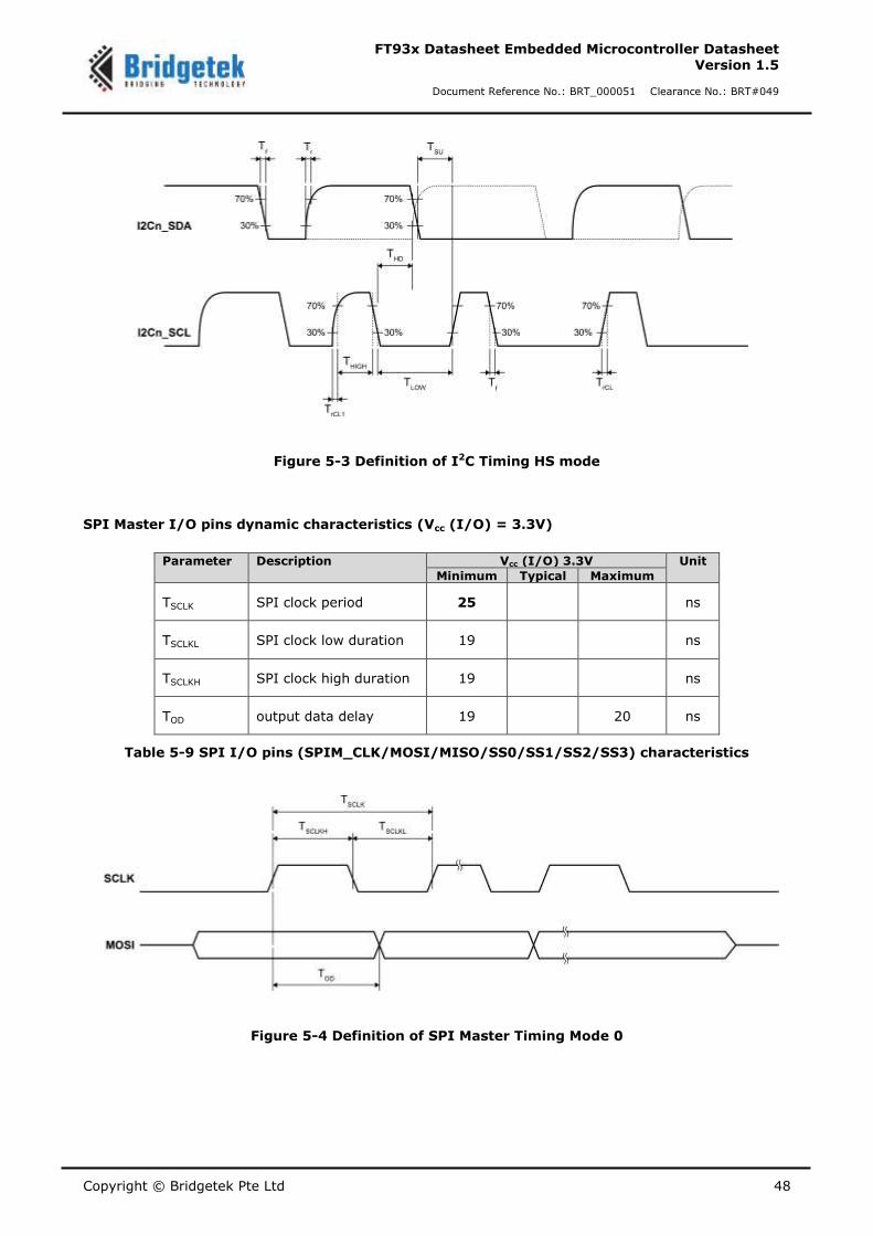
Copyright © Bridgetek Pte Ltd 48
FT93x Datasheet Embedded Microcontroller Datasheet Version 1.5
Document Reference No.: BRT_000051 Clearance No.: BRT#049
Figure 5-3 Definition of I2C Timing HS mode
SPI Master I/O pins dynamic characteristics (Vcc (I/O) = 3.3V)
Parameter Description Vcc (I/O) 3.3V Unit
Minimum Typical Maximum
TSCLK SPI clock period 25 ns
TSCLKL SPI clock low duration 19 ns
TSCLKH SPI clock high duration 19 ns
TOD output data delay 19 20 ns
Table 5-9 SPI I/O pins (SPIM_CLK/MOSI/MISO/SS0/SS1/SS2/SS3) characteristics
Figure 5-4 Definition of SPI Master Timing Mode 0
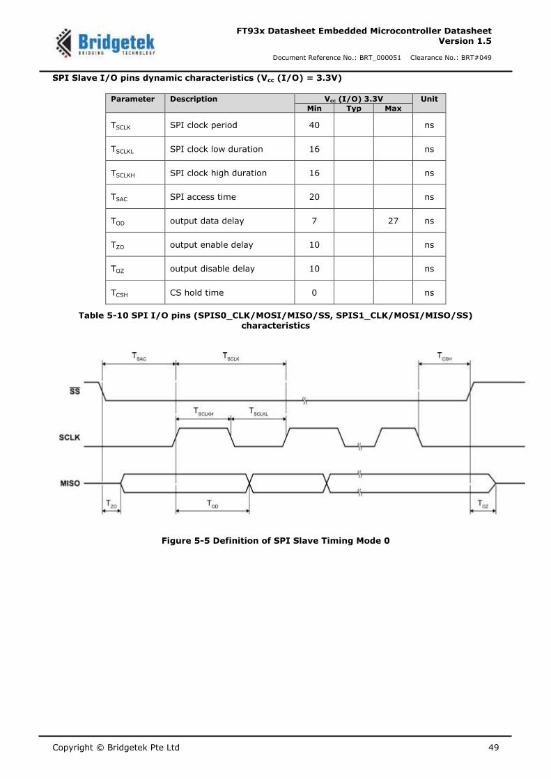
Copyright © Bridgetek Pte Ltd 49
FT93x Datasheet Embedded Microcontroller Datasheet Version 1.5
Document Reference No.: BRT_000051 Clearance No.: BRT#049
SPI Slave I/O pins dynamic characteristics (Vcc (I/O) = 3.3V)
Parameter Description Vcc (I/O) 3.3V Unit
Min Typ Max
TSCLK SPI clock period 40 ns
TSCLKL SPI clock low duration 16 ns
TSCLKH SPI clock high duration 16 ns
TSAC SPI access time 20 ns
TOD output data delay 7 27 ns
TZO output enable delay 10 ns
TOZ output disable delay 10 ns
TCSH CS hold time 0 ns
Table 5-10 SPI I/O pins (SPIS0_CLK/MOSI/MISO/SS, SPIS1_CLK/MOSI/MISO/SS) characteristics
Figure 5-5 Definition of SPI Slave Timing Mode 0
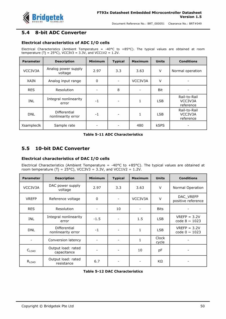
Copyright © Bridgetek Pte Ltd 50
FT93x Datasheet Embedded Microcontroller Datasheet Version 1.5
Document Reference No.: BRT_000051 Clearance No.: BRT#049
5.4 8-bit ADC Converter
Electrical characteristics of ADC I/O cells
Electrical Characteristics (Ambient Temperature = -40°C to +85°C). The typical values are obtained at room temperature (Tj = 25°C), VCC3V3 = 3.3V, and VCC1V2 = 1.2V.
Parameter Description Minimum Typical Maximum Units Conditions
VCC3V3A Analog power supply
voltage 2.97 3.3 3.63 V Normal operation
XAIN Analog input range 0 - VCC3V3A V -
RES Resolution - 8 - Bit -
INL Integral nonlinearity
error -1 - 1 LSB
Rail-to-Rail VCC3V3A reference
DNL Differential
nonlinearity error -1 - 1 LSB
Rail-to-Rail VCC3V3A reference
Xsampleclk Sample rate - - 480 kSPS -
Table 5-11 ADC Characteristics
5.5 10-bit DAC Converter
Electrical characteristics of DAC I/O cells
Electrical Characteristics (Ambient Temperature = -40°C to +85°C). The typical values are obtained at room temperature (Tj = 25°C), VCC3V3 = 3.3V, and VCC1V2 = 1.2V.
Parameter Description Minimum Typical Maximum Units Conditions
VCC3V3A DAC power supply
voltage 2.97 3.3 3.63 V Normal Operation
VREFP Reference voltage 0 - VCC3V3A V DAC_VREFP
positive reference
RES Resolution - 10 - Bits -
INL Integral nonlinearity
error -1.5 - 1.5 LSB
VREFP = 3.2V code 8 ~ 1023
DNL Differential
nonlinearity error -1 - 1 LSB
VREFP = 3.2V code 0 ~ 1023
- Conversion latency - - 1 Clock cycle
-
CLOAD Output load: rated
capacitance - - 10 pF -
RLOAD Output load: rated
resistance 6.7 - - KΩ -
Table 5-12 DAC Characteristics
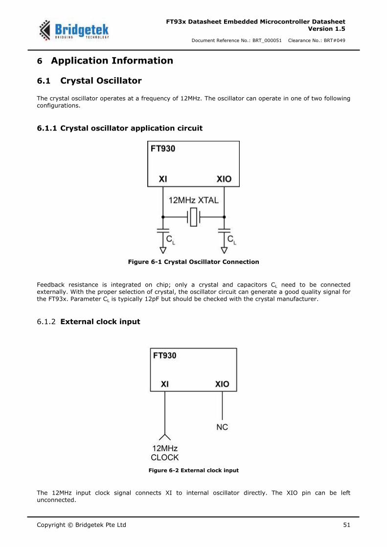
Copyright © Bridgetek Pte Ltd 51
FT93x Datasheet Embedded Microcontroller Datasheet Version 1.5
Document Reference No.: BRT_000051 Clearance No.: BRT#049
6 Application Information
6.1 Crystal Oscillator
The crystal oscillator operates at a frequency of 12MHz. The oscillator can operate in one of two following configurations.
6.1.1 Crystal oscillator application circuit
Figure 6-1 Crystal Oscillator Connection
Feedback resistance is integrated on chip; only a crystal and capacitors CL need to be connected externally. With the proper selection of crystal, the oscillator circuit can generate a good quality signal for the FT93x. Parameter CL is typically 12pF but should be checked with the crystal manufacturer.
6.1.2 External clock input
Figure 6-2 External clock input
The 12MHz input clock signal connects XI to internal oscillator directly. The XIO pin can be left unconnected.
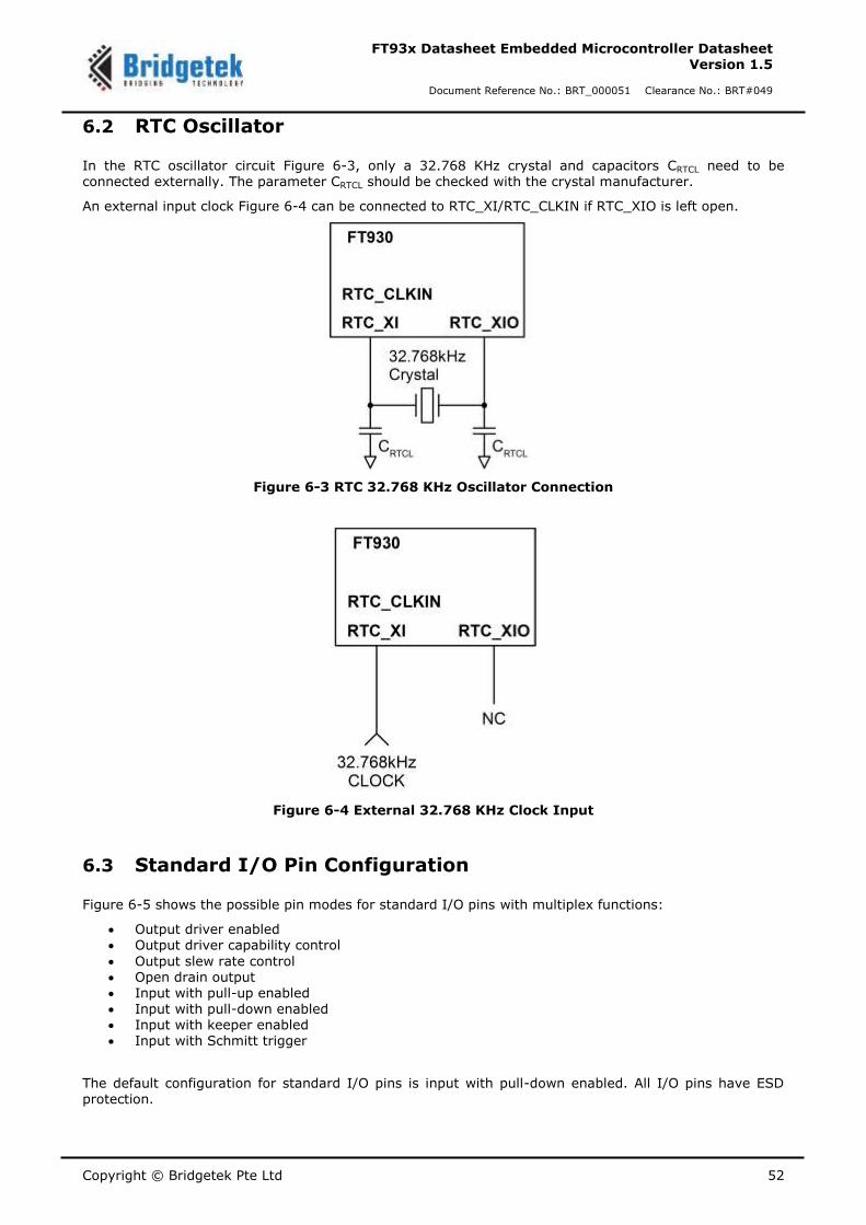
Copyright © Bridgetek Pte Ltd 52
FT93x Datasheet Embedded Microcontroller Datasheet Version 1.5
Document Reference No.: BRT_000051 Clearance No.: BRT#049
6.2 RTC Oscillator
In the RTC oscillator circuit Figure 6-3, only a 32.768 KHz crystal and capacitors CRTCL need to be connected externally. The parameter CRTCL should be checked with the crystal manufacturer.
An external input clock Figure 6-4 can be connected to RTC_XI/RTC_CLKIN if RTC_XIO is left open.
Figure 6-3 RTC 32.768 KHz Oscillator Connection
Figure 6-4 External 32.768 KHz Clock Input
6.3 Standard I/O Pin Configuration
Figure 6-5 shows the possible pin modes for standard I/O pins with multiplex functions:
Output driver enabled Output driver capability control
Output slew rate control Open drain output Input with pull-up enabled Input with pull-down enabled Input with keeper enabled Input with Schmitt trigger
The default configuration for standard I/O pins is input with pull-down enabled. All I/O pins have ESD protection.
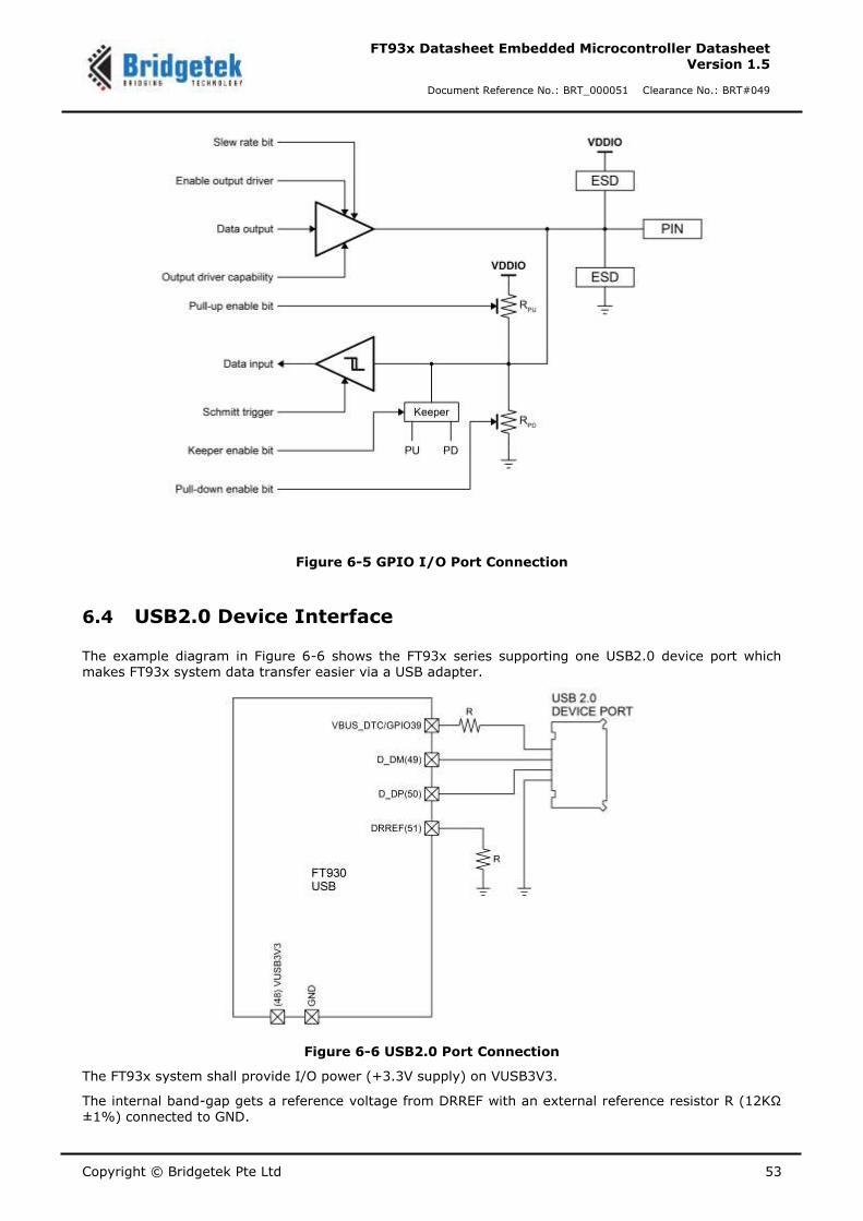
Copyright © Bridgetek Pte Ltd 53
FT93x Datasheet Embedded Microcontroller Datasheet Version 1.5
Document Reference No.: BRT_000051 Clearance No.: BRT#049
Figure 6-5 GPIO I/O Port Connection
6.4 USB2.0 Device Interface
The example diagram in Figure 6-6 shows the FT93x series supporting one USB2.0 device port which makes FT93x system data transfer easier via a USB adapter.
Figure 6-6 USB2.0 Port Connection
The FT93x system shall provide I/O power (+3.3V supply) on VUSB3V3.
The internal band-gap gets a reference voltage from DRREF with an external reference resistor R (12KΩ ±1%) connected to GND.
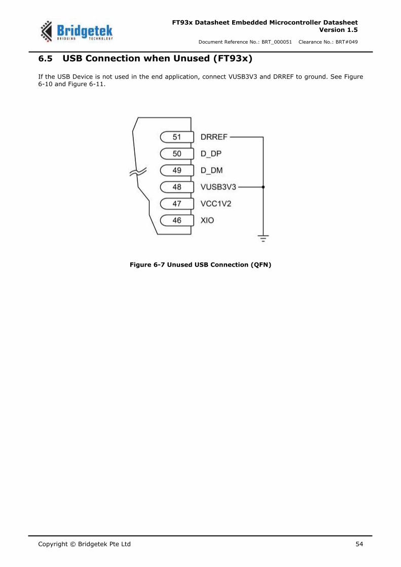
Copyright © Bridgetek Pte Ltd 54
FT93x Datasheet Embedded Microcontroller Datasheet Version 1.5
Document Reference No.: BRT_000051 Clearance No.: BRT#049
6.5 USB Connection when Unused (FT93x)
If the USB Device is not used in the end application, connect VUSB3V3 and DRREF to ground. See Figure 6-10 and Figure 6-11.
Figure 6-7 Unused USB Connection (QFN)
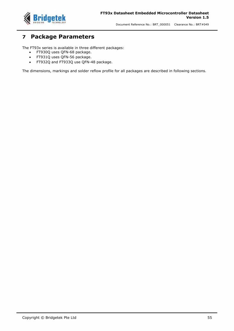
Copyright © Bridgetek Pte Ltd 55
FT93x Datasheet Embedded Microcontroller Datasheet Version 1.5
Document Reference No.: BRT_000051 Clearance No.: BRT#049
7 Package Parameters
The FT93x series is available in three different packages: FT930Q uses QFN-68 package.
FT931Q uses QFN-56 package.
FT932Q and FT933Q use QFN-48 package.
The dimensions, markings and solder reflow profile for all packages are described in following sections.
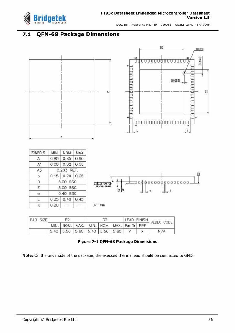
Copyright © Bridgetek Pte Ltd 56
FT93x Datasheet Embedded Microcontroller Datasheet Version 1.5
Document Reference No.: BRT_000051 Clearance No.: BRT#049
7.1 QFN-68 Package Dimensions
Figure 7-1 QFN-68 Package Dimensions
Note: On the underside of the package, the exposed thermal pad should be connected to GND.
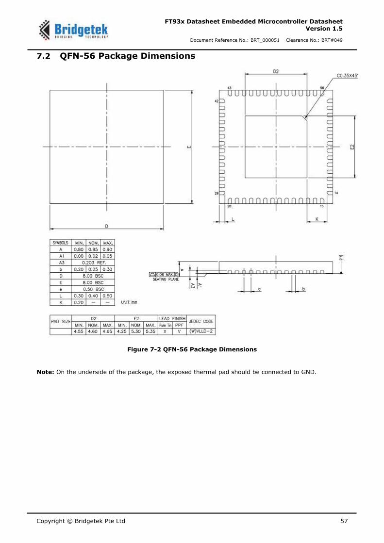
Copyright © Bridgetek Pte Ltd 57
FT93x Datasheet Embedded Microcontroller Datasheet Version 1.5
Document Reference No.: BRT_000051 Clearance No.: BRT#049
7.2 QFN-56 Package Dimensions
Figure 7-2 QFN-56 Package Dimensions
Note: On the underside of the package, the exposed thermal pad should be connected to GND.
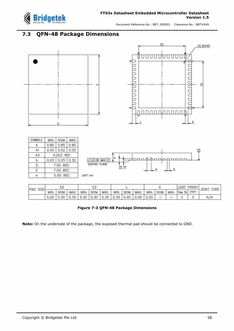
Copyright © Bridgetek Pte Ltd 58
FT93x Datasheet Embedded Microcontroller Datasheet Version 1.5
Document Reference No.: BRT_000051 Clearance No.: BRT#049
7.3 QFN-48 Package Dimensions
Figure 7-3 QFN-48 Package Dimensions
Note: On the underside of the package, the exposed thermal pad should be connected to GND.
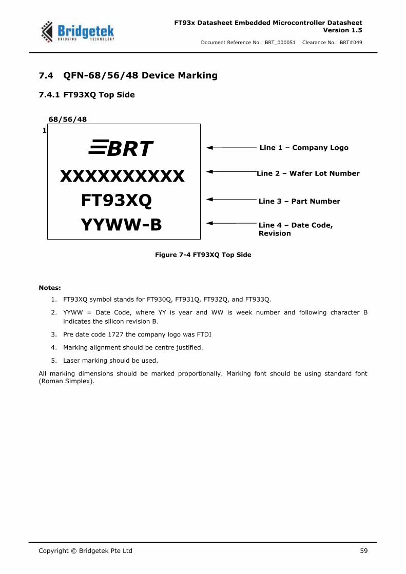
Copyright © Bridgetek Pte Ltd 59
FT93x Datasheet Embedded Microcontroller Datasheet Version 1.5
Document Reference No.: BRT_000051 Clearance No.: BRT#049
7.4 QFN-68/56/48 Device Marking
7.4.1 FT93XQ Top Side
Figure 7-4 FT93XQ Top Side
Notes:
1. FT93XQ symbol stands for FT930Q, FT931Q, FT932Q, and FT933Q.
2. YYWW = Date Code, where YY is year and WW is week number and following character B
indicates the silicon revision B.
3. Pre date code 1727 the company logo was FTDI
4. Marking alignment should be centre justified.
5. Laser marking should be used.
All marking dimensions should be marked proportionally. Marking font should be using standard font (Roman Simplex).
BRT
XXXXXXXXXX
FT93XQ
Line 1 – Company Logo
Line 4 – Date Code, Revision
Line 2 – Wafer Lot Number
1
68/56/48
Line 3 – Part Number
YYWW-B
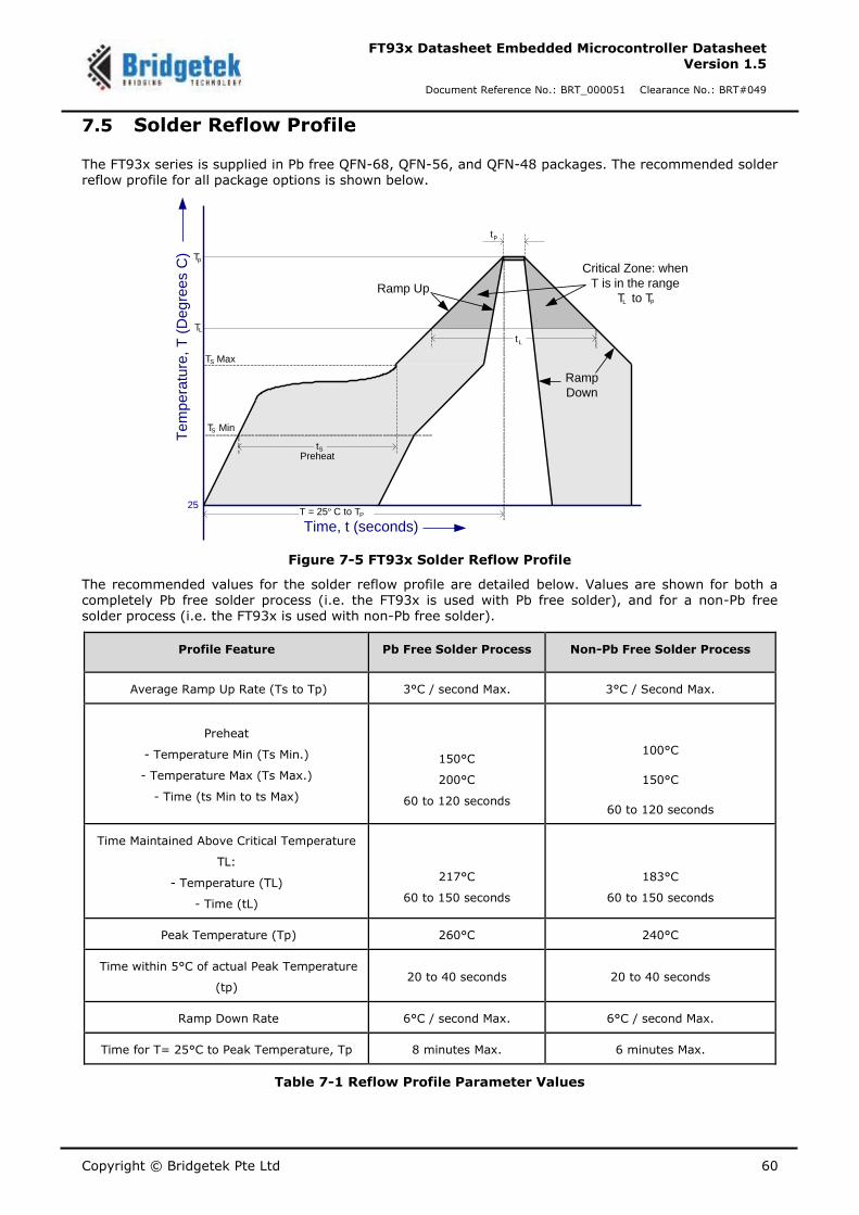
Copyright © Bridgetek Pte Ltd 60
FT93x Datasheet Embedded Microcontroller Datasheet Version 1.5
Document Reference No.: BRT_000051 Clearance No.: BRT#049
7.5 Solder Reflow Profile
The FT93x series is supplied in Pb free QFN-68, QFN-56, and QFN-48 packages. The recommended solder reflow profile for all package options is shown below.
Figure 7-5 FT93x Solder Reflow Profile
The recommended values for the solder reflow profile are detailed below. Values are shown for both a completely Pb free solder process (i.e. the FT93x is used with Pb free solder), and for a non-Pb free solder process (i.e. the FT93x is used with non-Pb free solder).
Profile Feature Pb Free Solder Process Non-Pb Free Solder Process
Average Ramp Up Rate (Ts to Tp) 3°C / second Max. 3°C / Second Max.
Preheat
- Temperature Min (Ts Min.)
- Temperature Max (Ts Max.)
- Time (ts Min to ts Max)
150°C
200°C
60 to 120 seconds
100°C
150°C
60 to 120 seconds
Time Maintained Above Critical Temperature
TL:
- Temperature (TL)
- Time (tL)
217°C
60 to 150 seconds
183°C
60 to 150 seconds
Peak Temperature (Tp) 260°C 240°C
Time within 5°C of actual Peak Temperature
(tp) 20 to 40 seconds 20 to 40 seconds
Ramp Down Rate 6°C / second Max. 6°C / second Max.
Time for T= 25°C to Peak Temperature, Tp 8 minutes Max. 6 minutes Max.
Table 7-1 Reflow Profile Parameter Values
Critical Zone: when
T is in the range
T to T
Tem
pe
ratu
re,
T (
Deg
rees C
)
Time, t (seconds)
25PT = 25º C to T
tp
Tp
TL
tPreheat
S
tL
Ramp UpL p
Ramp
Down
T MaxS
T MinS
Copyright © Bridgetek Pte Ltd 61
FT93x Datasheet Embedded Microcontroller Datasheet Version 1.5
Document Reference No.: BRT_000051 Clearance No.: BRT#049
8 Contact Information
Headquarters – Singapore Branch Office – Taipei, Taiwan
Bridgetek Pte Ltd 178 Paya Lebar Road, #07-03 Singapore 409030 Tel: +65 6547 4827 Fax: +65 6841 6071
Bridgetek Pte Ltd, Taiwan Branch 2 Floor, No. 516, Sec. 1, Nei Hu Road, Nei Hu District Taipei 114 Taiwan, R.O.C. Tel: +886 (2) 8797 5691 Fax: +886 (2) 8751 9737
E-mail (Sales) [email protected] E-mail (Sales) [email protected] E-mail (Support) [email protected] E-mail (Support) [email protected]
Branch Office - Glasgow, United Kingdom Branch Office – Vietnam
Bridgetek Pte Ltd. Unit 1, 2 Seaward Place, Centurion Business Park Glasgow G41 1HH United Kingdom Tel: +44 (0) 141 429 2777 Fax: +44 (0) 141 429 2758
Bridgetek VietNam Company Limited Lutaco Tower Building, 5th Floor, 173A Nguyen Van Troi, Ward 11, Phu Nhuan District, Ho Chi Minh City, Vietnam Tel : 08 38453222 Fax : 08 38455222
E-mail (Sales) [email protected] E-mail (Sales) [email protected] E-mail (Support) [email protected] E-mail (Support) [email protected]
Web Site
http://brtchip.com/
Distributor and Sales Representatives
Please visit the Sales Network page of the Bridgetek Web site for the contact details of our distributor(s) and sales representative(s) in your country.
System and equipment manufacturers and designers are responsible to ensure that their systems, and any Bridgetek Pte Ltd (BRT
Chip) devices incorporated in their systems, meet all applicable safety, regulatory and system-level performance requirements. All
application-related information in this document (including application descriptions, suggested Bridgetek devices and other materials) is
provided for reference only. While Bridgetek has taken care to assure it is accurate, this information is subject to customer
confirmation, and Bridgetek disclaims all liability for system designs and for any applications assistance provided by Bridgetek. Use of
Bridgetek devices in life support and/or safety applications is entirely at the user’s risk, and the user agrees to defend, indemnify and
hold harmless Bridgetek from any and all damages, claims, suits or expense resulting from such use. This document is subject to
change without notice. No freedom to use patents or other intellectual property rights is implied by the publication of this document.
Neither the whole nor any part of the information contained in, or the product described in this document, may be adapted or
reproduced in any material or electronic form without the prior written consent of the copyright holder. Bridgetek Pte Ltd, 178 Paya Lebar Road, #07-03, Singapore 409030. Singapore Registered Company Number: 201542387H.
Copyright © Bridgetek Pte Ltd 62
FT93x Datasheet Embedded Microcontroller Datasheet Version 1.5
Document Reference No.: BRT_000051 Clearance No.: BRT#049
Appendix A – References
Document References
BRT_AN_010_ FT93x_User_Manual
AN_341 FT32_Technical_Manual
FT900 toolchain
AN_325 _ Toolchain Installation Guide
Sample firmware
Acronyms and Abbreviations
Terms Description
ADC Analog-to-Digital Converter
BCD Battery Charge Device
CDP Charging Downstream Port
DAC Digital-to-Analog Converter
DAQ Data Acquisition
DCP Dedicated Charging Port
DNL Differential Nonlinearity
FIFO First In First Out
GPIO General Purpose Input / Output
INL Integral Nonlinearity
I/O Input/Output
LSB Least Significant Bit
MMC Multimedia Card
MSPS Mega Samples Per Second
NMI Non-Maskable Interrupt input
POR Power On Reset
PWM Pulse Width Modulator
QFN Quad Flat No-Lead
RTC Real Time Clock
SD Secure Digital
SDIO Secure Digital Input Output
SDP Standard Downstream Port
SPI Serial Peripheral Interface
UART Universal Asynchronous Receiver/Transmitter
UHS Ultra High Speed
USB Universal Serial Bus
Copyright © Bridgetek Pte Ltd 63
FT93x Datasheet Embedded Microcontroller Datasheet Version 1.5
Document Reference No.: BRT_000051 Clearance No.: BRT#049
Appendix B - List of Figures and Tables
List of Figures
Figure 2-1 FT930 68-pin Block Diagram ........................................................................................... 4
Figure 3-1 Pin Configuration FT930Q (top-down view) ....................................................................... 8
Figure 3-2 Pin Configuration FT931Q (top-down view) ....................................................................... 9
Figure 3-3 Pin Configuration FT932Q (top-down view) ..................................................................... 10
Figure 3-4 Pin Configuration FT933Q (top-down view) ..................................................................... 11
Figure 5-1 USB Rise and Fall Times for DP/DM ............................................................................... 46
Figure 5-2 Definition of I2C Timing F/S mode ................................................................................. 47
Figure 5-3 Definition of I2C Timing HS mode .................................................................................. 48
Figure 5-4 Definition of SPI Master Timing Mode 0 .......................................................................... 48
Figure 5-5 Definition of SPI Slave Timing Mode 0 ............................................................................ 49
Figure 6-1 Crystal Oscillator Connection ........................................................................................ 51
Figure 6-2 External clock input ..................................................................................................... 51
Figure 6-3 RTC 32.768 KHz Oscillator Connection ........................................................................... 52
Figure 6-4 External 32.768 KHz Clock Input ................................................................................... 52
Figure 6-5 GPIO I/O Port Connection ............................................................................................. 53
Figure 6-6 USB2.0 Port Connection ............................................................................................... 53
Figure 6-7 Unused USB Connection (QFN)...................................................................................... 54
Figure 7-1 QFN-68 Package Dimensions ........................................................................................ 56
Figure 7-2 QFN-56 Package Dimensions ........................................................................................ 57
Figure 7-3 QFN-48 Package Dimensions ........................................................................................ 58
Figure 7-4 FT93XQ Top Side......................................................................................................... 59
Figure 7-5 FT93x Solder Reflow Profile .......................................................................................... 60
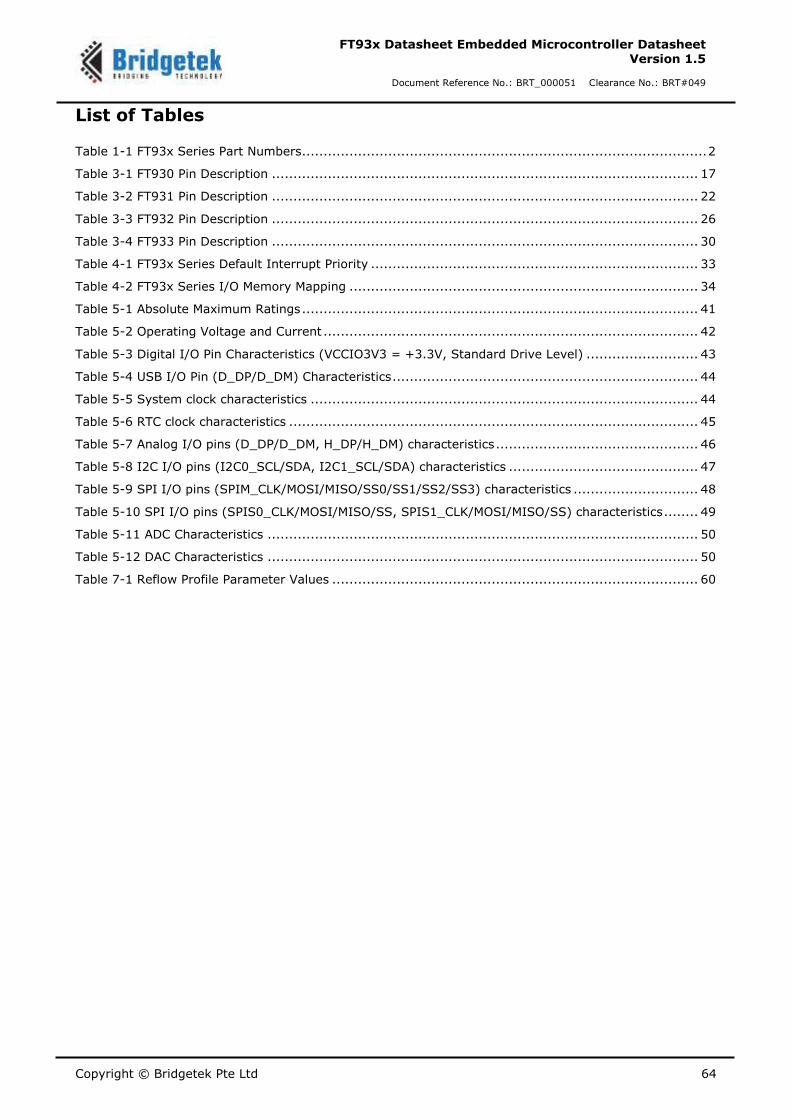
Copyright © Bridgetek Pte Ltd 64
FT93x Datasheet Embedded Microcontroller Datasheet Version 1.5
Document Reference No.: BRT_000051 Clearance No.: BRT#049
List of Tables
Table 1-1 FT93x Series Part Numbers .............................................................................................. 2
Table 3-1 FT930 Pin Description ................................................................................................... 17
Table 3-2 FT931 Pin Description ................................................................................................... 22
Table 3-3 FT932 Pin Description ................................................................................................... 26
Table 3-4 FT933 Pin Description ................................................................................................... 30
Table 4-1 FT93x Series Default Interrupt Priority ............................................................................ 33
Table 4-2 FT93x Series I/O Memory Mapping ................................................................................. 34
Table 5-1 Absolute Maximum Ratings ............................................................................................ 41
Table 5-2 Operating Voltage and Current ....................................................................................... 42
Table 5-3 Digital I/O Pin Characteristics (VCCIO3V3 = +3.3V, Standard Drive Level) .......................... 43
Table 5-4 USB I/O Pin (D_DP/D_DM) Characteristics ....................................................................... 44
Table 5-5 System clock characteristics .......................................................................................... 44
Table 5-6 RTC clock characteristics ............................................................................................... 45
Table 5-7 Analog I/O pins (D_DP/D_DM, H_DP/H_DM) characteristics ............................................... 46
Table 5-8 I2C I/O pins (I2C0_SCL/SDA, I2C1_SCL/SDA) characteristics ............................................ 47
Table 5-9 SPI I/O pins (SPIM_CLK/MOSI/MISO/SS0/SS1/SS2/SS3) characteristics ............................. 48
Table 5-10 SPI I/O pins (SPIS0_CLK/MOSI/MISO/SS, SPIS1_CLK/MOSI/MISO/SS) characteristics ........ 49
Table 5-11 ADC Characteristics .................................................................................................... 50
Table 5-12 DAC Characteristics .................................................................................................... 50
Table 7-1 Reflow Profile Parameter Values ..................................................................................... 60
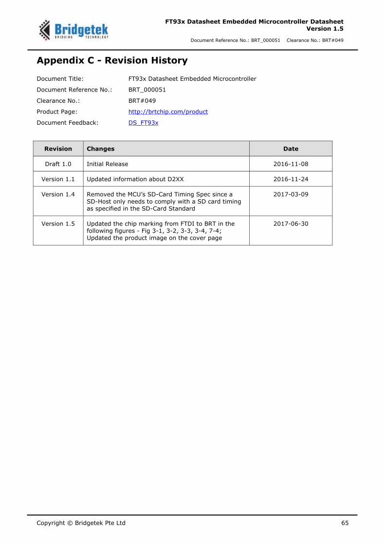
Copyright © Bridgetek Pte Ltd 65
FT93x Datasheet Embedded Microcontroller Datasheet Version 1.5
Document Reference No.: BRT_000051 Clearance No.: BRT#049
Appendix C - Revision History
Document Title: FT93x Datasheet Embedded Microcontroller
Document Reference No.: BRT_000051
Clearance No.: BRT#049
Product Page: http://brtchip.com/product
Document Feedback: DS_FT93x
Revision Changes Date
Draft 1.0 Initial Release 2016-11-08
Version 1.1 Updated information about D2XX 2016-11-24
Version 1.4 Removed the MCU’s SD-Card Timing Spec since a
SD-Host only needs to comply with a SD card timing as specified in the SD-Card Standard
2017-03-09
Version 1.5 Updated the chip marking from FTDI to BRT in the following figures - Fig 3-1, 3-2, 3-3, 3-4, 7-4; Updated the product image on the cover page
2017-06-30