Embed Size (px)
Citation preview

Future Technology Devices International Limited (FTDI) Unit 1,2 Seaward Place, Glasgow G41 1HH, United Kingdom
Tel.: +44 (0) 141 429 2777 Fax: + 44 (0) 141 429 2758 E-Mail (Support): [email protected] Web: http://www.ftdichip.com
Copyright © 2012 Future Technology Devices International Limited
Future Technology Devices International Ltd
Application Note AN_114
Interfacing FT2232H Hi-Speed Devices
To SPI Bus
Document Reference No. FT_000149
Version 1.1
Issue Date: 2012-08-08
This application note introduces the SPI synchronous serial communication interface, and illustrates how to implement SPI with
the FT2232H. The FT2232H will be used to write and read data to a SPI serial EEPROM.

1
Copyright © 2012 Future Technology Devices International Limited
Document Reference No.: FT_000149 Interfacing FT2232H Hi-Speed Devices To SPI Bus Application Note AN_114
Version 1.1 Clearance No.: FTDI# 115
Table of Contents
1 Introduction............................................................................................ 2
1.1 Overview & Scope ............................................................................................... 2
1.2 Overview of SPI Interface.................................................................................... 2
1.3 FT2232H/FT4232H SPI Pinout ............................................................................. 4
2 SPI Design Example .............................................................................. 5
3 Sample SPI Program Code Overview .................................................... 6
3.1 C++ Code Listing ................................................................................................. 7
3.2 FT2232H to 93LC56 Read/Write Timing on Scope ......................................... 15
4 Acronyms and Abbreviations ............................................................. 18
5 Contact Information............................................................................. 19
Appendix A - References .......................................................................... 21
Appendix B - List of Figures and Tables .................................................. 22
Appendix C - Revision History .................................................................. 23

2
Copyright © 2012 Future Technology Devices International Limited
Document Reference No.: FT_000149 Interfacing FT2232H Hi-Speed Devices To SPI Bus Application Note AN_114
Version 1.1 Clearance No.: FTDI# 115
1 Introduction
The FT2232H and FT4232H are the FTDI’s first USB 2.0 Hi-Speed (480Mbits/s) USB to UART/FIFO ICs. They have the capability of being configured in a variety of serial interfaces using the internal MPSSE (Multi-Protocol Synchronous Serial Engine). The FT2232H device has two independent ports, both of which can be configured using MPSSE while only Channel A and B of FT4232H can be configured using MPSSE.
Using MPSSE can simplify the synchronous serial protocol (USB to SPI, I2C, JTAG, etc.) design. This
application note illustrates how to use the MPSSE of the FT2232H to interface with the SPI bus. Users can use the example schematic (refer to Figure 3) and functional software code (section 3) to begin their design.
Note that the example software is for illustration and is neither guaranteed nor supported by FTDI.
1.1 Overview & Scope
This application note gives details of how to interface and configure the FT2232H to read and write data from a host PC to a serial EEPROM over the serial SPI interface bus. This note includes:
Overview of SPI communications interface.
Hardware example of a USB to a serial EEPROM SPI interface using the FT2232H.
Code example in C++ showing how to configure the FT2232H in SPI mode.
Oscilloscope plots showing example SPI read and write cycles.
1.2 Overview of SPI Interface
The SPI (Serial to Peripheral Interface) is a master/slave synchronous serial bus that consists of 4 signals. Both command signals and data are sent across the interface. The SPI master initiates all data transactions. Full duplex data transfers can be made up to 30 Mbits/sec with the FT2232H. There is no fixed bit length in SPI. A generic SPI system consists of the following signals and is illustrated in Figure 1.
Serial Clock (SCLK) from master to slave.
Serial Data Out (also called Master Out Slave In or MOSI) from master.
Serial Data In (also called Master In Slave Out or MISO) from slave.
Chip Select (CS) from master.
Figure 1 Generic SPI System

3
Copyright © 2012 Future Technology Devices International Limited
Document Reference No.: FT_000149 Interfacing FT2232H Hi-Speed Devices To SPI Bus Application Note AN_114
Version 1.1 Clearance No.: FTDI# 115
The FT2232H always acts as the SPI master. Multiple slave devices can be enabled by multiplexing the chip select line. As SPI data is shifted out of the master and in to a slave device, SPI data will also be shifted out from the slave and clocked in to the master. Depending on which type of slave device is being implemented, data can be shifted MSB first or LSB first. Slave devices can have active low or active high chip select inputs. Figure 2 shows an example SPI timing diagram.
Figure 2 Example SPI Timing Diagram
This SPI device uses SPI Mode 0, with active low Chip Select
In addition, the SPI interface has 4 unique modes of clock phase (CPHA) and clock polarity (CPOL), known as Mode 0, Mode 1, Mode 2 and Mode 3. Table 1 summarizes these modes.
For CPOL = 0, the base (inactive) level of SCLK is 0.
In this mode:
When CPHA = 0, data will be read in on the rising edge of SCLK, and data will be clocked out on the falling edge of SCLK.
When CPHA = 1, data will be read in on the falling edge of SCLK, and data will clocked out on the rising edge of SCLK
For CPOL =1, the base (inactive) level of SCLK is 1.
In this mode:
When CPHA = 0, data will be read in on the falling edge of SCLK, and data will clocked out on the rising edge of SCLK
When CPHA =1, data will be read in on the rising edge of SCLK, and data will be clocked out on the falling edge of SCLK.
Mode CPOL CPHA
0 0 0
1 0 1
2 1 0
3 1 1
Table 1 Clock Phase/Polarity Modes
It is worth noting that the SPI slave interface can be implemented in various ways. The FT2232H can be configured to handle these different implementations.
It is recommended that designers review the SPI Slave data sheet to determine the SPI mode implementation.FTDI device can only support mode 0 and mode 2 due to the limitation of MPSSE engine.

4
Copyright © 2012 Future Technology Devices International Limited
Document Reference No.: FT_000149 Interfacing FT2232H Hi-Speed Devices To SPI Bus Application Note AN_114
Version 1.1 Clearance No.: FTDI# 115
1.3 FT2232H/FT4232H SPI Pinout
These tables show the location and function of the SPI signal pins on Channel A and B of the FT2232H and FT4232H devices.
Channel A
FT2232H Pin# FT4232H Pin# Pin Name MPSEE Function Type Description
16 16 ADBUS0 SCLK Output Serial Clock
17 17 ADBUS1 DO (MOSI) Output Master Out
18 18 ADBUS2 DI (MISO) Input Master In
19 19 ADBUS3 CS Output Chip Select
Channel B
FT2232H Pin# FT4232H Pin# Pin Name MPSEE Function Type Description
38 26 BDBUS0 SCLK Output Serial Clock
39 27 BDBUS1 DO (MOSI) Output Master Out
40 28 BDBUS2 DI (MISO) Input Master In
41 29 BDBUS3 CS Output Chip Select
Table 2 FT2232H/4232H SPI Pinout

5
Copyright © 2012 Future Technology Devices International Limited
Document Reference No.: FT_000149 Interfacing FT2232H Hi-Speed Devices To SPI Bus Application Note AN_114
Version 1.1 Clearance No.: FTDI# 115
2 SPI Design Example
The following design, using the FT2232H, demonstrates how to configure the SPI communication with a Microchip 93LC56 Serial SPI EEPROM. A simplified diagram, Figure 3, illustrates the connections.
For clarity, only the Channel A SPI Pins are shown in figure 3.
Please refer to the FT2232H datasheet & the 93LC56 datasheet for interface details.
The sections which follow provide the user with some example code for setting up the SPI interface.
FT2232H Datasheet
93LC56 Datasheet
Figure 3 FT2232H to 93LC56 EEPROM

6
Copyright © 2012 Future Technology Devices International Limited
Document Reference No.: FT_000149 Interfacing FT2232H Hi-Speed Devices To SPI Bus Application Note AN_114
Version 1.1 Clearance No.: FTDI# 115
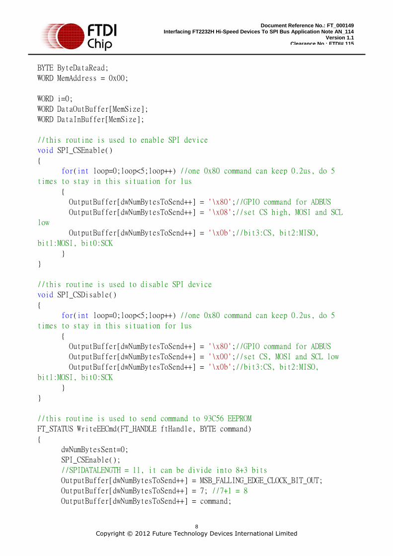
3 Sample SPI Program Code Overview
The sample code provided in the following section configures the FT2232H to function in SPI mode.
The code first verifies that a FTDI Hi Speed device is plugged in, and then identifies the device as either a FT2232H or FT4232H.
Next, the SPI application sends a command to erase the entire EEPROM, and then writes a 16 bit word to the EEPROM.
After each write cycle, the address counter and the data counter are incremented. The new address and data are written to the next memory location.
After 128 bytes of data is written, the application reads back the data and verifies that a successful write of 128 addresses has taken place.
The 128 byte write/read process can be repeated by changing the ”LoopCntr” parameter on page 14.
The code example uses the FTCSPI dll, and requires the use of Microsoft Visual Studio 2008 C++.
The source code for this project can be downloaded from:
http://www.ftdichip.com/Projects/MPSSE/FT2232HS_SPI.zip
The code requires the FTDI D2XX driver:
D2XX Driver link
More information on the D2XX API can be found in the D2XX Programmer’s Guide:
D2XX Programmer's Guide

7
Copyright © 2012 Future Technology Devices International Limited
Document Reference No.: FT_000149 Interfacing FT2232H Hi-Speed Devices To SPI Bus Application Note AN_114
Version 1.1 Clearance No.: FTDI# 115
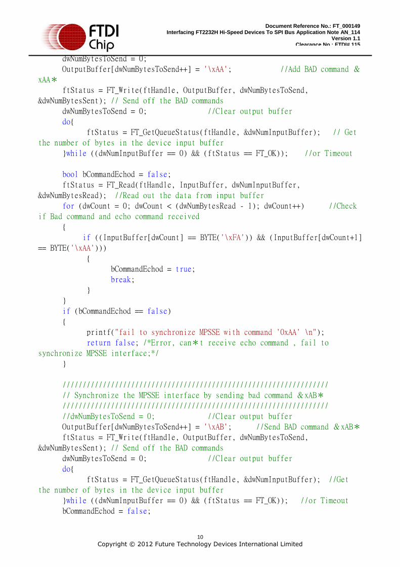
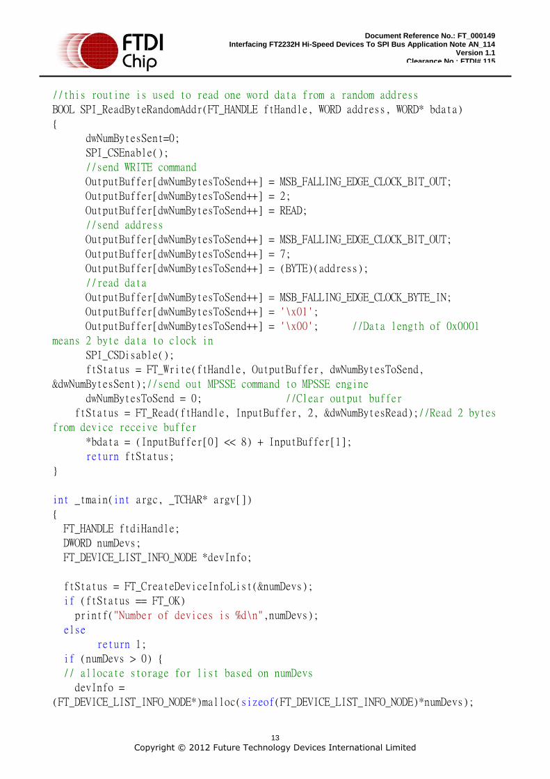
3.1 C++ Code Listing
//
// SPITEST.cpp : VC++ console application.
// this example project use port A of FT2232H to access SPI EEPROM 93C56
// we send 16 word data to 93C56 and read them back, user can see the test
// result in command mode.
#include "stdafx.h"
#include <windows.h>
#include "FTD2XX.h"
#include <stdlib.h>
//declare parameters for 93C56
#define MemSize 16 //define data quantity you want to send out
const BYTE SPIDATALENGTH = 11;//3 digit command + 8 digit address
const BYTE READ = '\xC0';//110xxxxx
const BYTE WRITE = '\xA0';//101xxxxx
const BYTE WREN = '\x98';//10011xxx
const BYTE ERAL = '\x90';//10010xxx
//declare for BAD command
const BYTE AA_ECHO_CMD_1 = '\xAA';
const BYTE AB_ECHO_CMD_2 = '\xAB';
const BYTE BAD_COMMAND_RESPONSE = '\xFA';
//declare for MPSSE command
const BYTE MSB_RISING_EDGE_CLOCK_BYTE_OUT = '\x10';
const BYTE MSB_FALLING_EDGE_CLOCK_BYTE_OUT = '\x11';
const BYTE MSB_RISING_EDGE_CLOCK_BIT_OUT = '\x12';
const BYTE MSB_FALLING_EDGE_CLOCK_BIT_OUT = '\x13';
const BYTE MSB_RISING_EDGE_CLOCK_BYTE_IN = '\x20';
const BYTE MSB_RISING_EDGE_CLOCK_BIT_IN = '\x22';
const BYTE MSB_FALLING_EDGE_CLOCK_BYTE_IN = '\x24';
const BYTE MSB_FALLING_EDGE_CLOCK_BIT_IN = '\x26';
FT_STATUS ftStatus; //Status defined in D2XX to indicate
operation result
BYTE OutputBuffer[512]; //Buffer to hold MPSSE commands and data to be
sent to FT2232H
BYTE InputBuffer[512]; //Buffer to hold Data bytes to be read from
FT2232H
DWORD dwClockDivisor = 29; //Value of clock divisor, SCL Frequency =
60/((1+29)*2) (MHz) = 1Mhz
DWORD dwNumBytesToSend = 0; //Index of output buffer
DWORD dwNumBytesSent = 0, dwNumBytesRead = 0, dwNumInputBuffer = 0;
8
Copyright © 2012 Future Technology Devices International Limited
Document Reference No.: FT_000149 Interfacing FT2232H Hi-Speed Devices To SPI Bus Application Note AN_114
Version 1.1 Clearance No.: FTDI# 115
BYTE ByteDataRead;
WORD MemAddress = 0x00;
WORD i=0;
WORD DataOutBuffer[MemSize];
WORD DataInBuffer[MemSize];
//this routine is used to enable SPI device
void SPI_CSEnable()
{
for(int loop=0;loop<5;loop++) //one 0x80 command can keep 0.2us, do 5
times to stay in this situation for 1us
{
OutputBuffer[dwNumBytesToSend++] = '\x80';//GPIO command for ADBUS
OutputBuffer[dwNumBytesToSend++] = '\x08';//set CS high, MOSI and SCL
low
OutputBuffer[dwNumBytesToSend++] = '\x0b';//bit3:CS, bit2:MISO,
bit1:MOSI, bit0:SCK
}
}
//this routine is used to disable SPI device
void SPI_CSDisable()
{
for(int loop=0;loop<5;loop++) //one 0x80 command can keep 0.2us, do 5
times to stay in this situation for 1us
{
OutputBuffer[dwNumBytesToSend++] = '\x80';//GPIO command for ADBUS
OutputBuffer[dwNumBytesToSend++] = '\x00';//set CS, MOSI and SCL low
OutputBuffer[dwNumBytesToSend++] = '\x0b';//bit3:CS, bit2:MISO,
bit1:MOSI, bit0:SCK
}
}
//this routine is used to send command to 93C56 EEPROM
FT_STATUS WriteEECmd(FT_HANDLE ftHandle, BYTE command)
{
dwNumBytesSent=0;
SPI_CSEnable();
//SPIDATALENGTH = 11, it can be divide into 8+3 bits
OutputBuffer[dwNumBytesToSend++] = MSB_FALLING_EDGE_CLOCK_BIT_OUT;
OutputBuffer[dwNumBytesToSend++] = 7; //7+1 = 8
OutputBuffer[dwNumBytesToSend++] = command;
9
Copyright © 2012 Future Technology Devices International Limited
Document Reference No.: FT_000149 Interfacing FT2232H Hi-Speed Devices To SPI Bus Application Note AN_114
Version 1.1 Clearance No.: FTDI# 115
OutputBuffer[dwNumBytesToSend++] = MSB_FALLING_EDGE_CLOCK_BIT_OUT;
OutputBuffer[dwNumBytesToSend++] = SPIDATALENGTH - (8+1);
OutputBuffer[dwNumBytesToSend++] = '\xff';
SPI_CSDisable();
ftStatus = FT_Write(ftHandle, OutputBuffer, dwNumBytesToSend,
&dwNumBytesSent); //send MPSSE command to MPSSE engine.
dwNumBytesToSend = 0; //Clear output buffer
return ftStatus;
}
//this routine is used to initial SPI interface
BOOL SPI_Initial(FT_HANDLE ftHandle)
{
DWORD dwCount;
ftStatus = FT_ResetDevice(ftHandle); //Reset USB device
//Purge USB receive buffer first by reading out all old data from FT2232H
receive buffer
ftStatus |= FT_GetQueueStatus(ftHandle, &dwNumInputBuffer); // Get the
number of bytes in the FT2232H receive buffer
if ((ftStatus == FT_OK) && (dwNumInputBuffer > 0))
ftStatus |= FT_Read(ftHandle, InputBuffer, dwNumInputBuffer,
&dwNumBytesRead); //Read out the data from FT2232H receive buffer
ftStatus |= FT_SetUSBParameters(ftHandle, 65535, 65535); //Set USB
request transfer size
ftStatus |= FT_SetChars(ftHandle, false, 0, false, 0); //Disable
event and error characters
ftStatus |= FT_SetTimeouts(ftHandle, 3000, 3000); //Sets the
read and write timeouts in 3 sec for the FT2232H
ftStatus |= FT_SetLatencyTimer(ftHandle, 1); //Set the latency
timer
ftStatus |= FT_SetBitMode(ftHandle, 0x0, 0x00); //Reset
controller
ftStatus |= FT_SetBitMode(ftHandle, 0x0, 0x02); //Enable MPSSE mode
if (ftStatus != FT_OK)
{
printf("fail on initialize FT2232H device ! \n");
return false;
}
Sleep(50); // Wait 50ms for all the USB stuff to complete and work
//////////////////////////////////////////////////////////////////
// Synchronize the MPSSE interface by sending bad command &xAA*
//////////////////////////////////////////////////////////////////
10
Copyright © 2012 Future Technology Devices International Limited
Document Reference No.: FT_000149 Interfacing FT2232H Hi-Speed Devices To SPI Bus Application Note AN_114
Version 1.1 Clearance No.: FTDI# 115
dwNumBytesToSend = 0;
OutputBuffer[dwNumBytesToSend++] = '\xAA'; //Add BAD command &
xAA*
ftStatus = FT_Write(ftHandle, OutputBuffer, dwNumBytesToSend,
&dwNumBytesSent); // Send off the BAD commands
dwNumBytesToSend = 0; //Clear output buffer
do{
ftStatus = FT_GetQueueStatus(ftHandle, &dwNumInputBuffer); // Get
the number of bytes in the device input buffer
}while ((dwNumInputBuffer == 0) && (ftStatus == FT_OK)); //or Timeout
bool bCommandEchod = false;
ftStatus = FT_Read(ftHandle, InputBuffer, dwNumInputBuffer,
&dwNumBytesRead); //Read out the data from input buffer
for (dwCount = 0; dwCount < (dwNumBytesRead - 1); dwCount++) //Check
if Bad command and echo command received
{
if ((InputBuffer[dwCount] == BYTE('\xFA')) && (InputBuffer[dwCount+1]
== BYTE('\xAA')))
{
bCommandEchod = true;
break;
}
}
if (bCommandEchod == false)
{
printf("fail to synchronize MPSSE with command '0xAA' \n");
return false; /*Error, can*t receive echo command , fail to
synchronize MPSSE interface;*/
}
//////////////////////////////////////////////////////////////////
// Synchronize the MPSSE interface by sending bad command &xAB*
//////////////////////////////////////////////////////////////////
//dwNumBytesToSend = 0; //Clear output buffer
OutputBuffer[dwNumBytesToSend++] = '\xAB'; //Send BAD command &xAB*
ftStatus = FT_Write(ftHandle, OutputBuffer, dwNumBytesToSend,
&dwNumBytesSent); // Send off the BAD commands
dwNumBytesToSend = 0; //Clear output buffer
do{
ftStatus = FT_GetQueueStatus(ftHandle, &dwNumInputBuffer); //Get
the number of bytes in the device input buffer
}while ((dwNumInputBuffer == 0) && (ftStatus == FT_OK)); //or Timeout
bCommandEchod = false;

11
Copyright © 2012 Future Technology Devices International Limited
Document Reference No.: FT_000149 Interfacing FT2232H Hi-Speed Devices To SPI Bus Application Note AN_114
Version 1.1 Clearance No.: FTDI# 115
ftStatus = FT_Read(ftHandle, InputBuffer, dwNumInputBuffer,
&dwNumBytesRead); //Read out the data from input buffer
for (dwCount = 0;dwCount < (dwNumBytesRead - 1); dwCount++) //Check if Bad
command and echo command received
{
if ((InputBuffer[dwCount] == BYTE('\xFA')) && (InputBuffer[dwCount+1]
== BYTE( '\xAB')))
{
bCommandEchod = true;
break;
}
}
if (bCommandEchod == false)
{
printf("fail to synchronize MPSSE with command '0xAB' \n");
return false;
/*Error, can't receive echo command , fail to synchronize MPSSE
interface;*/
}
////////////////////////////////////////////////////////////////////
//Configure the MPSSE for SPI communication with EEPROM
//////////////////////////////////////////////////////////////////
OutputBuffer[dwNumBytesToSend++] = '\x8A'; //Ensure disable clock divide by
5 for 60Mhz master clock
OutputBuffer[dwNumBytesToSend++] = '\x97'; //Ensure turn off adaptive
clocking
OutputBuffer[dwNumBytesToSend++] = '\x8D'; //disable 3 phase data clock
ftStatus = FT_Write(ftHandle, OutputBuffer, dwNumBytesToSend,
&dwNumBytesSent); // Send out the commands
dwNumBytesToSend = 0; //Clear output buffer
OutputBuffer[dwNumBytesToSend++] = '\x80'; //Command to set directions of
lower 8 pins and force value on bits set as output
OutputBuffer[dwNumBytesToSend++] = '\x00'; //Set SDA, SCL high, WP disabled
by SK, DO at bit &*, GPIOL0 at bit &*
OutputBuffer[dwNumBytesToSend++] = '\x0b'; //Set SK,DO,GPIOL0 pins as
output with bit **, other pins as input with bit &*
// The SK clock frequency can be worked out by below algorithm with divide
by 5 set as off
// SK frequency = 60MHz /((1 + [(1 +0xValueH*256) OR 0xValueL])*2)
OutputBuffer[dwNumBytesToSend++] = '\x86'; //Command to set
clock divisor
OutputBuffer[dwNumBytesToSend++] = BYTE(dwClockDivisor & '\xFF'); //Set
0xValueL of clock divisor
OutputBuffer[dwNumBytesToSend++] = BYTE(dwClockDivisor >> 8); //Set 0xValueH

12
Copyright © 2012 Future Technology Devices International Limited
Document Reference No.: FT_000149 Interfacing FT2232H Hi-Speed Devices To SPI Bus Application Note AN_114
Version 1.1 Clearance No.: FTDI# 115
of clock divisor
ftStatus = FT_Write(ftHandle, OutputBuffer, dwNumBytesToSend,
&dwNumBytesSent); // Send out the commands
dwNumBytesToSend = 0; //Clear output buffer
Sleep(20); //Delay for a while
//Turn off loop back in case
OutputBuffer[dwNumBytesToSend++] = '\x85'; //Command to turn off loop
back of TDI/TDO connection
ftStatus = FT_Write(ftHandle, OutputBuffer, dwNumBytesToSend,
&dwNumBytesSent); // Send out the commands
dwNumBytesToSend = 0; //Clear output buffer
Sleep(30); //Delay for a while
printf("SPI initial successful\n");
return true;
}
//this routine is used to write one word data to a random address
BOOL SPI_WriteByte2RandomAddr(FT_HANDLE ftHandle, WORD address,WORD bdata)
{
dwNumBytesSent=0;
SPI_CSEnable();
//send WRITE command
OutputBuffer[dwNumBytesToSend++] = MSB_FALLING_EDGE_CLOCK_BIT_OUT;
OutputBuffer[dwNumBytesToSend++] = 2;
OutputBuffer[dwNumBytesToSend++] = WRITE;
//send address
OutputBuffer[dwNumBytesToSend++] = MSB_FALLING_EDGE_CLOCK_BIT_OUT;
OutputBuffer[dwNumBytesToSend++] = 7;
OutputBuffer[dwNumBytesToSend++] = (BYTE)(address);
//send data
OutputBuffer[dwNumBytesToSend++] = MSB_FALLING_EDGE_CLOCK_BYTE_OUT;
OutputBuffer[dwNumBytesToSend++] = 1;
OutputBuffer[dwNumBytesToSend++] = 0;//Data length of 0x0001 means 2 byte
data to clock out
OutputBuffer[dwNumBytesToSend++] = bdata >> 8;//output high byte
OutputBuffer[dwNumBytesToSend++] = bdata & 0xff;//output low byte
SPI_CSDisable();
ftStatus = FT_Write(ftHandle, OutputBuffer, dwNumBytesToSend,
&dwNumBytesSent);//send out MPSSE command to MPSSE engine
dwNumBytesToSend = 0; //Clear output buffer
return ftStatus;
}
13
Copyright © 2012 Future Technology Devices International Limited
Document Reference No.: FT_000149 Interfacing FT2232H Hi-Speed Devices To SPI Bus Application Note AN_114
Version 1.1 Clearance No.: FTDI# 115
//this routine is used to read one word data from a random address
BOOL SPI_ReadByteRandomAddr(FT_HANDLE ftHandle, WORD address, WORD* bdata)
{
dwNumBytesSent=0;
SPI_CSEnable();
//send WRITE command
OutputBuffer[dwNumBytesToSend++] = MSB_FALLING_EDGE_CLOCK_BIT_OUT;
OutputBuffer[dwNumBytesToSend++] = 2;
OutputBuffer[dwNumBytesToSend++] = READ;
//send address
OutputBuffer[dwNumBytesToSend++] = MSB_FALLING_EDGE_CLOCK_BIT_OUT;
OutputBuffer[dwNumBytesToSend++] = 7;
OutputBuffer[dwNumBytesToSend++] = (BYTE)(address);
//read data
OutputBuffer[dwNumBytesToSend++] = MSB_FALLING_EDGE_CLOCK_BYTE_IN;
OutputBuffer[dwNumBytesToSend++] = '\x01';
OutputBuffer[dwNumBytesToSend++] = '\x00'; //Data length of 0x0001
means 2 byte data to clock in
SPI_CSDisable();
ftStatus = FT_Write(ftHandle, OutputBuffer, dwNumBytesToSend,
&dwNumBytesSent);//send out MPSSE command to MPSSE engine
dwNumBytesToSend = 0; //Clear output buffer
ftStatus = FT_Read(ftHandle, InputBuffer, 2, &dwNumBytesRead);//Read 2 bytes
from device receive buffer
*bdata = (InputBuffer[0] << 8) + InputBuffer[1];
return ftStatus;
}
int _tmain(int argc, _TCHAR* argv[])
{
FT_HANDLE ftdiHandle;
DWORD numDevs;
FT_DEVICE_LIST_INFO_NODE *devInfo;
ftStatus = FT_CreateDeviceInfoList(&numDevs);
if (ftStatus == FT_OK)
printf("Number of devices is %d\n",numDevs);
else
return 1;
if (numDevs > 0) {
// allocate storage for list based on numDevs
devInfo =
(FT_DEVICE_LIST_INFO_NODE*)malloc(sizeof(FT_DEVICE_LIST_INFO_NODE)*numDevs);

14
Copyright © 2012 Future Technology Devices International Limited
Document Reference No.: FT_000149 Interfacing FT2232H Hi-Speed Devices To SPI Bus Application Note AN_114
Version 1.1 Clearance No.: FTDI# 115
// get the device information list
ftStatus = FT_GetDeviceInfoList(devInfo,&numDevs);
if (ftStatus == FT_OK) {
for (i = 0; i < numDevs; i++) {
printf("Dev %d:\n",i);
printf(" Flags=0x%x\n",devInfo[i].Flags);
printf(" Type=0x%x\n",devInfo[i].Type);
printf(" ID=0x%x\n",devInfo[i].ID);
printf(" LocId=0x%x\n",devInfo[i].LocId);
printf(" SerialNumber=%s\n",devInfo[i].SerialNumber);
printf(" Description=%s\n",devInfo[i].Description);
printf(" ftHandle=0x%x\n",devInfo[i].ftHandle);
}
}
}
else
return 1;
ftStatus = FT_Open(0,&ftdiHandle);
if (ftStatus != FT_OK)
{
printf("Can't open FT2232H device! \n");
return 1;
}
else // Port opened successfully
printf("Successfully open FT2232H device! \n");
if(SPI_Initial(ftdiHandle) == TRUE)
{
byte ReadByte = 0;
//initial output buffer
for(i=0;i<MemSize;i++)
DataOutBuffer[i] = i;
//Purge USB received buffer first before read operation
ftStatus = FT_GetQueueStatus(ftdiHandle, &dwNumInputBuffer); // Get
the number of bytes in the device receive buffer
if ((ftStatus == FT_OK) && (dwNumInputBuffer > 0))
FT_Read(ftdiHandle, InputBuffer, dwNumInputBuffer,
&dwNumBytesRead); //Read out all the data from receive buffer
WriteEECmd(ftdiHandle, WREN);
WriteEECmd(ftdiHandle, ERAL);
Sleep(20);

15
Copyright © 2012 Future Technology Devices International Limited
Document Reference No.: FT_000149 Interfacing FT2232H Hi-Speed Devices To SPI Bus Application Note AN_114
Version 1.1 Clearance No.: FTDI# 115
for(i=0;i<MemSize;i++)
{
SPI_WriteByte2RandomAddr(ftdiHandle, i,DataOutBuffer[i]);
Sleep(2);
printf("Write data %d to address %d\n",DataOutBuffer[i],i);
}
Sleep(20);
for(i=0;i<MemSize;i++)
{
SPI_ReadByteRandomAddr(ftdiHandle, i,&DataInBuffer[i]);
printf("Read data from address %d = %d\n",i,DataInBuffer[i]);
}
getchar();//wait here until we get a key press.
}
FT_Close(ftdiHandle);
return 0;
}
3.2 FT2232H to 93LC56 Read/Write Timing on Scope
The following screenshots show examples of the Read and write waveforms on the SPI interface. These are provided to illustrate the operational details of the SPI write and read commands sent from the FT2232H to the 93LC56 EEPROM.

16
Copyright © 2012 Future Technology Devices International Limited
Document Reference No.: FT_000149 Interfacing FT2232H Hi-Speed Devices To SPI Bus Application Note AN_114
Version 1.1 Clearance No.: FTDI# 115
Figure 4 Write 3 to Address 3
The Figure 4 screen capture shows a write command (101) applied to MOSI, followed by a 3 written to address 3.

17
Copyright © 2012 Future Technology Devices International Limited
Document Reference No.: FT_000149 Interfacing FT2232H Hi-Speed Devices To SPI Bus Application Note AN_114
Version 1.1 Clearance No.: FTDI# 115
Figure 5 Read 3 from Address 3
The Figure 5 screen capture shows a Read command applied to MOSI (110), followed by the address 3. The MOSI output shows the data read (3).
18
Copyright © 2012 Future Technology Devices International Limited
Document Reference No.: FT_000149 Interfacing FT2232H Hi-Speed Devices To SPI Bus Application Note AN_114
Version 1.1 Clearance No.: FTDI# 115
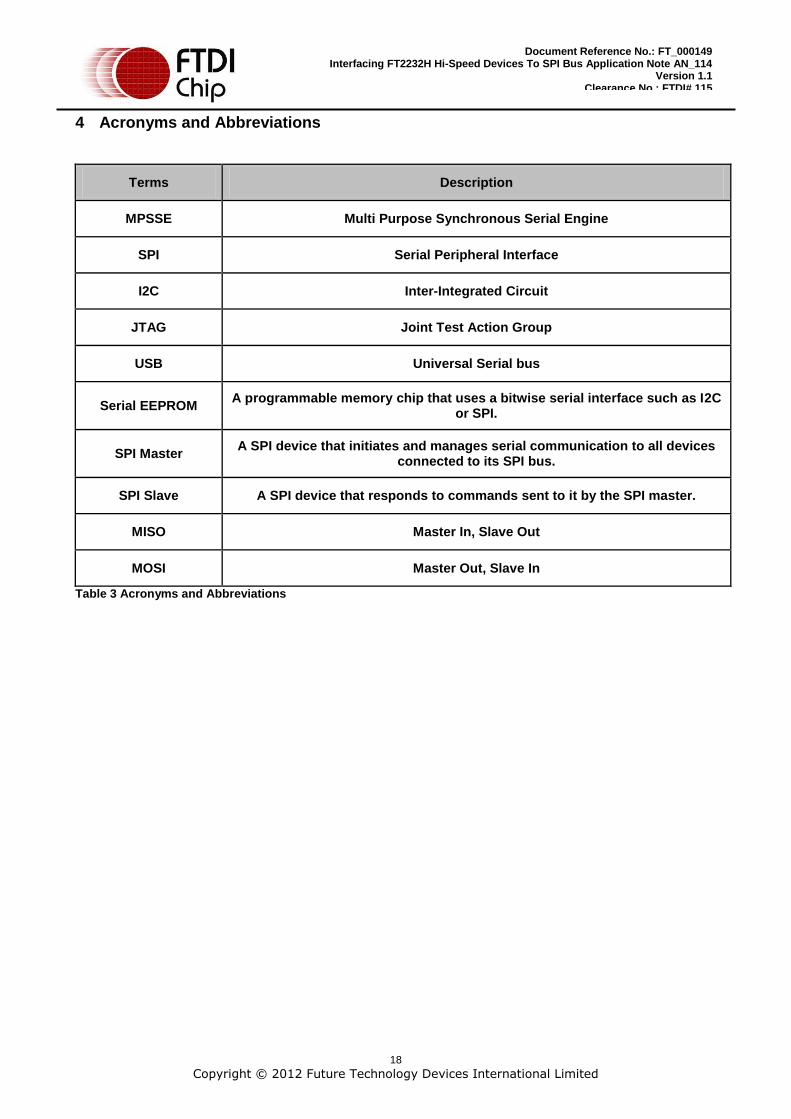
4 Acronyms and Abbreviations
Terms Description
MPSSE Multi Purpose Synchronous Serial Engine
SPI Serial Peripheral Interface
I2C Inter-Integrated Circuit
JTAG Joint Test Action Group
USB Universal Serial bus
Serial EEPROM A programmable memory chip that uses a bitwise serial interface such as I2C
or SPI.
SPI Master A SPI device that initiates and manages serial communication to all devices
connected to its SPI bus.
SPI Slave A SPI device that responds to commands sent to it by the SPI master.
MISO Master In, Slave Out
MOSI Master Out, Slave In
Table 3 Acronyms and Abbreviations

19
Copyright © 2012 Future Technology Devices International Limited
Document Reference No.: FT_000149 Interfacing FT2232H Hi-Speed Devices To SPI Bus Application Note AN_114
Version 1.1 Clearance No.: FTDI# 115
5 Contact Information
Head Office – Glasgow, UK Future Technology Devices International Limited
Unit 1,2 Seaward Place, Centurion Business Park Glasgow G41 1HH United Kingdom Tel: +44 (0) 141 429 2777 Fax: +44 (0) 141 429 2758 E-mail (Sales) [email protected]
E-mail (Support) [email protected] E-mail (General Enquiries) [email protected]
Web Site URL http://www.ftdichip.com Web Shop URL http://www.ftdichip.com
Branch Office – Taipei, Taiwan Future Technology Devices International Limited (Taiwan)
2F, No. 516, Sec. 1, NeiHu Road Taipei 114 Taiwan , R.O.C. Tel: +886 (0) 2 8797 1330 Fax: +886 (0) 2 8751 9737
E-mail (Sales) [email protected]
E-mail (Support) [email protected] E-mail (General Enquiries) [email protected] Web Site URL http://www.ftdichip.com
Branch Office – Hillsboro, Oregon, USA Future Technology Devices International Limited (USA) 7235 NW Evergreen Parkway, Suite 600
Hillsboro, OR 97123-5803 USA Tel: +1 (503) 547 0988 Fax: +1 (503) 547 0987 E-Mail (Sales) [email protected]
E-Mail (Support) [email protected]
Web Site URL http://www.ftdichip.com
Branch Office – Shanghai, China Future Technology Devices International Limited (China) Room 1103, No. 666,
West Huaihai Road, Shanghai, 200052 China
Tel: +86 21 62351596 Fax: +86 21 62351595 E-mail (Sales) [email protected] E-mail (Support) [email protected]
E-mail (General Enquiries) [email protected]
Web Site URL http://www.ftdichip.com

20
Copyright © 2012 Future Technology Devices International Limited
Document Reference No.: FT_000149 Interfacing FT2232H Hi-Speed Devices To SPI Bus Application Note AN_114
Version 1.1 Clearance No.: FTDI# 115
Distributors and Sales Representatives Please visit the Sales Network page of the FTDI Web site for the contact details of our distributor(s) in your country.
Neither the whole nor any part of the information contained in, or the product described in this manual, may be adapted or reproduced in any material or electronic form without the prior written consent of the copyright holder. This product and its documentation are supplied on an as-is basis and no warranty as to their suitability for any particular purpose is either made or implied. Future Technology Devices International Ltd will not accept any claim for damages howsoever arising as a result of use or failure of this product. Your statutory rights are not affected. This product or any variant of it is not intended for use in any medical appliance, device or system in which the failure of the product might reasonably be expected to result in personal injury. This document provides preliminary information that may be subject to change without notice. No freedom to use patents or other intellectual property rights is implied by the publication of this document. Future Technology Devices International Ltd, Unit 1, 2 Seaward Place, Centurion Business Park, Glasgow G41 1HH United Kingdom. Scotland Registered Number: SC136640

21
Copyright © 2012 Future Technology Devices International Limited
Document Reference No.: FT_000149 Interfacing FT2232H Hi-Speed Devices To SPI Bus Application Note AN_114
Version 1.1 Clearance No.: FTDI# 115
Appendix A - References
FTCSPI Programmer’s Guide
D2XX Programmer’s Guide
Datasheet for FT2232H
Datasheet for 93C56 Serial EEPROM

22
Copyright © 2012 Future Technology Devices International Limited
Document Reference No.: FT_000149 Interfacing FT2232H Hi-Speed Devices To SPI Bus Application Note AN_114
Version 1.1 Clearance No.: FTDI# 115
Appendix B - List of Figures and Tables
List of Figures
Figure 1 Generic SPI System .......................................................................................................................... 2
Figure 2 Example SPI Timing Diagram ......................................................................................................... 3
Figure 3 FT2232H to 93LC56 EEPROM ......................................................................................................... 5
Figure 4 Write 3 to Address 3 ...................................................................................................................... 16
Figure 5 Read 3 from Address 3 ................................................................................................................. 17
List of Tables
Table 1 Clock Phase/Polarity Modes ............................................................................................................ 3
Table 2 FT2232H/4232H SPI Pinout ............................................................................................................... 4
Table 3 Acronyms and Abbreviations ......................................................................................................... 18

23
Copyright © 2012 Future Technology Devices International Limited
Document Reference No.: FT_000149 Interfacing FT2232H Hi-Speed Devices To SPI Bus Application Note AN_114
Version 1.1 Clearance No.: FTDI# 115
Appendix C - Revision History
Revision History
Version 1.0 Initial Release 20th October, 2009
Version 1.1 Update SPI sample code 8th
August 2012