Embed Size (px)
Citation preview
Use of FTDI devices in life support and/or safety applications is entirely at the user’s risk, and the user agrees to defend, indemnify and hold harmless FTDI from any and all damages, claims, suits or expense resulting
from such use.
Future Technology Devices International Limited (FTDI) Unit 1, 2 Seaward Place, Glasgow G41 1HH, United Kingdom Tel.: +44 (0) 141 429 2777 Fax: + 44 (0) 141 429 2758
Web Site: http://ftdichip.com Copyright © 2014 Future Technology Devices International Limited
Future Technology Devices International
Application Note
AN_201
FT-X MTP memory Configuration
2.0
Issue Date: 2013-12-18
This application note describes the MTP Memory Map of the FTDI FT-X series of
chips. This MTP memory is used for storing configuration data in the FT-X series of devices. The MTP Memory can be read and written over USB on all FT-X series
devices, and can also be read and written over I2C on the members of the FT-X family which include I2C interfaces.
This application note only covers the MTP memory map. It does not cover the methods of reading and writing the memory. These are covered in the individual device datasheet and the D2XX Programmers Guide.
1
Copyright © 2014 Future Technology Devices International Limited
Application Note
AN_201 FT-X MTP memory Configuration 2.0
Document Reference No.: FT_000572 Clearance No.: 298
Table of Contents
1 Introduction .................................................................... 3
2 Overview of the MTP Memory .......................................... 4
2.1 Memory Areas ........................................................................... 4
2.2 Reading and Writing Commands ............................................... 4
2.3 Programming over I2C and USB ................................................ 4
2.4 Important Warnings and Notes ................................................. 5
3 Memory Map .................................................................... 6
3.1 Memory Map Diagram ............................................................... 6
4 User Data Area ................................................................ 8
5 String descriptor Data ..................................................... 9
6 FTDI Configuration Data ............................................... 10
7 Configuration Descriptor data ....................................... 11
7.1 Misc Config ............................................................................. 11
7.2 USB VID .................................................................................. 12
7.3 USB PID .................................................................................. 12
7.4 BCD Release Number .............................................................. 12
7.5 Max Power & Config Description Value ................................... 12
7.6 Device & Peripheral Control .................................................... 13
7.7 DBUS & CBUS Control .............................................................. 14
7.8 Manufacturer String Descriptor ............................................... 14
7.9 Product String Descriptor ....................................................... 14
7.10 Serial Number String Descriptor ............................................. 14
7.11 I2C Address + Options ............................................................ 15
7.12 CBUS[6:0] Mux Control .......................................................... 15
8 Calculating the Checksum ............................................. 18
8.1 Checksum Calculation Example ............................................... 19
9 Contact Information ...................................................... 21
Appendix A – References ................................................... 22
Document References ..................................................................... 22
Acronyms and Abbreviations ........................................................... 22
2
Copyright © 2014 Future Technology Devices International Limited
Application Note
AN_201 FT-X MTP memory Configuration 2.0
Document Reference No.: FT_000572 Clearance No.: 298
Appendix B – List of Tables & Figures ................................ 23
Appendix C – Revision History ........................................... 24

3
Copyright © 2014 Future Technology Devices International Limited
Application Note
AN_201 FT-X MTP memory Configuration 2.0
Document Reference No.: FT_000572 Clearance No.: 298
1 Introduction
This application note describes the internal MTP (Multi-Time Programmable) memory map configuration area of the FT-X devices, also known as the X-Chip Series. This memory is used to hold information such as the Vendor ID, Product ID, String Descriptors, I2C address and functions assigned to each available Control Bus (CBUS) pin.
The MTP memory is available in all FT-X series devices and performs the same function as the internal EEPROM in the FT232R/FT245R devices.
This document details the data stored in each word of the MTP memory map so that a user application
can determine which values to write to configure the chip.
This application note does not cover the User area of MTP memory or the details of writing the values to the MTP (over I2C or USB). These are covered in the datasheet for each FT-X device and also in the D2XX Programmers Guide.

4
Copyright © 2014 Future Technology Devices International Limited
Application Note
AN_201 FT-X MTP memory Configuration 2.0
Document Reference No.: FT_000572 Clearance No.: 298
2 Overview of the MTP Memory
2.1 Memory Areas
There are two main areas of MTP memory, which are the User area and the Configuration area. A more detailed memory map is provided in the following section.
User Area
This area can be used for storing application-specific data, for example a calibration constant in an analog
measurement system. It is not used for chip configuration. This can be useful as it can avoid the cost and space needed to fit a separate EEPROM chip on the application board when only a few values need to be stored.
User area programming is not covered in the remainder of this document as it is covered in the FT-X device datasheet (for programming over I2C in devices which include an I2C interface) and in the D2XX
Programmers Guide for all FT-X devices. Note that the user area is not included in the MTP checksum and
so modification of the user area does not require re-calculation of the checksum.
Note: An application intending to write to the user area of the MTP memory should take care not to unintentionally change any data in the configuration area.
Configuration Area The device is initially supplied with the configuration areas of the MTP memory already programmed with default values and so in many cases the device can be used without any MTP programming at all.
Changing the contents of the Configuration areas of the MTP memory programming is only required when the final application requires the settings to be customised.
Some examples of customising the configuration settings include:
When the FT-X is to be given a custom Vendor (VID) and/or Product ID (PID) When the FT-X is to be given a specific serial number When the application requires different settings on the CBUS pins e.g. to configure the pins to
output the functional signals necessary for battery charging as shown in Application Note,
AN_175 (see References Section).
2.2 Reading and Writing Commands
This application note covers the memory map itself but does not cover the methods of reading and writing the memory, because this depends on the interface used. Further details on the read and write
commands themselves can be found in the following documents:
For applications which will read and write the MTP memory over I2C, the device datasheet contains the commands required to read and write the MTP memory. This includes the FT200XD and FT201X.
For applications which will program the MTP memory over USB, the D2xx Programmers Guide contains the commands required to read and write MTP memory. This includes all members of the FT-X device family.
2.3 Programming over I2C and USB
FTDI provide two methods of programming the MTP memory. These are designed to make it as easy and as efficient as possible to do this whether executed as part of the production/test process or the final application.

5
Copyright © 2014 Future Technology Devices International Limited
Application Note
AN_201 FT-X MTP memory Configuration 2.0
Document Reference No.: FT_000572 Clearance No.: 298
Programming the MTP memory over USB
The MTP memory on all FT-X devices can be programmed over USB. This method is similar to the other FTDI devices such as the FT232R. No additional hardware, connections or programming voltages are
required. The device is simply connected to the host computer in the same way that it would be for normal applications, and the programming is carried out over USB.
There are two methods for programming over USB:
FTDI provide a utility called FT_Prog which can be used to program the MTP memory. This utility provides a graphical user interface and can be used to configure the device without needing to know the actual memory map. The FT-Prog utility is provided free-of-charge from the FTDI website, and can be found at the link below. Please use the latest version available. The user
guide is also available at this link. Note that the FT-X devices require FT_Prog version 2.6.8 or later. http://www.ftdichip.com/Support/Utilities.htm#FT_Prog
D2XX commands can also be used to program the MTP memory from within user applications. For more information on the commands available, please see the D2XX Programmers Guide (See
Reference [2] in Appendix A – References). The remainder of this document can be used to determine the values in each location in order to configure the device as required.
Note that when programming over USB, word addresses are used.
Programming the MTP memory over I2C
In FT-X devices with I2C interfaces, it is also possible to program the MTP memory over I2C by using special commands.
This can be beneficial when no USB host is available to configure the MTP memory. For example, a bed-
of-nails test jig where no host is present as part of a production and test set-up. Also, if the FT-X is acting as a bridge between a microcontroller/FPGA and a USB host as part of an application, the microcontroller/FPGA can modify or program the MTP memory data. This could include changes to the configuration data (such as serial number) and/or storing application data in the user area of the MTP memory.
Note that when programming over I2C, byte addresses are used.
2.4 Important Warnings and Notes
Care must be taken when performing write operations on the MTP memory
Failure to recalculate a checksum after changing any of the configuration areas may prevent correct operation. An incorrect checksum will cause the device to use default values.
Modifying the MTP data may cause errors and can completely change the operation of the chip.
Ensure that the effect of the modification has been considered before writing the new value to MTP memory. For example, switching to the external oscillator mode will prevent the device from running from its internal oscillator. This cannot be changed back unless an external crystal is temporarily connected to allow the MTP memory to be programmed to select the internal clock source again.
It should be verified that the application code causes only the intended area to be modified and
that the value written is valid for that MTP memory location. For example, an application intending to write to the user area of the MTP memory should include safeguards to ensure that it does not unintentionally write to an address in the configuration area. Values written should also be valid values according to the tables in the following section.
Ensure that the application takes account of the MTP memory write cycle specification in the
datasheet of the FT-X device.
6
Copyright © 2014 Future Technology Devices International Limited
Application Note
AN_201 FT-X MTP memory Configuration 2.0
Document Reference No.: FT_000572 Clearance No.: 298
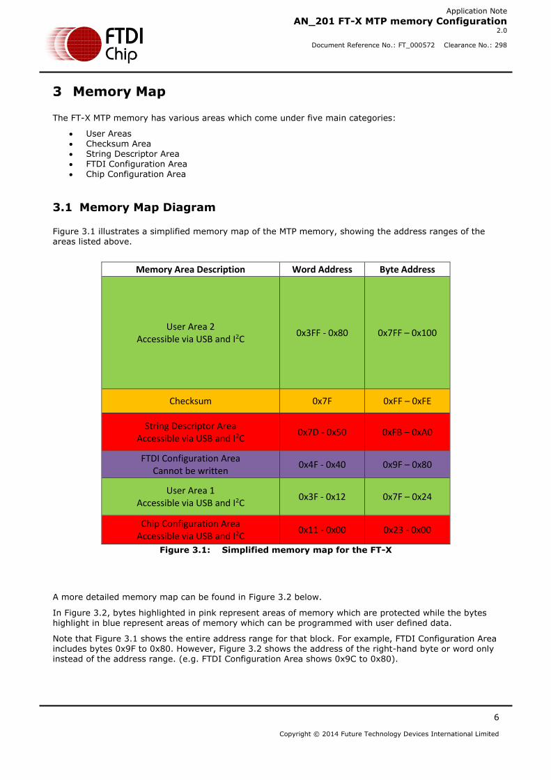
3 Memory Map
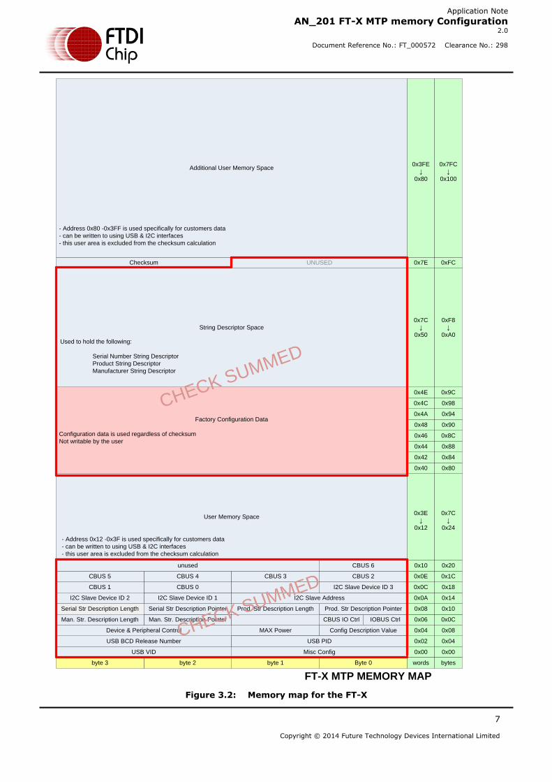
The FT-X MTP memory has various areas which come under five main categories:
User Areas Checksum Area String Descriptor Area FTDI Configuration Area Chip Configuration Area
3.1 Memory Map Diagram
Figure 3.1 illustrates a simplified memory map of the MTP memory, showing the address ranges of the areas listed above.
Memory Area Description Word Address Byte Address
User Area 2 Accessible via USB and I2C
0x3FF - 0x80 0x7FF – 0x100
Checksum 0x7F 0xFF – 0xFE
String Descriptor Area Accessible via USB and I2C
0x7D - 0x50 0xFB – 0xA0
FTDI Configuration Area Cannot be written
0x4F - 0x40 0x9F – 0x80
User Area 1 Accessible via USB and I2C
0x3F - 0x12 0x7F – 0x24
Chip Configuration Area Accessible via USB and I2C
0x11 - 0x00 0x23 - 0x00
Figure 3.1: Simplified memory map for the FT-X
A more detailed memory map can be found in Figure 3.2 below.
In Figure 3.2, bytes highlighted in pink represent areas of memory which are protected while the bytes highlight in blue represent areas of memory which can be programmed with user defined data.
Note that Figure 3.1 shows the entire address range for that block. For example, FTDI Configuration Area includes bytes 0x9F to 0x80. However, Figure 3.2 shows the address of the right-hand byte or word only instead of the address range. (e.g. FTDI Configuration Area shows 0x9C to 0x80).
7
Copyright © 2014 Future Technology Devices International Limited
Application Note
AN_201 FT-X MTP memory Configuration 2.0
Document Reference No.: FT_000572 Clearance No.: 298
FT-X MTP MEMORY MAP
USB BCD Release Number
MAX PowerDevice & Peripheral Control
IOBUS CtrlMan. Str. Description Pointer
Prod. Str Description LengthSerial Str Description Length
I2C Slave Device ID 1
CBUS 0
CBUS 4
Byte 0byte 1byte 2byte 3
Misc ConfigUSB VID
CBUS IO CtrlMan. Str. Description Length
Config Description Value
Prod. Str Description PointerSerial Str Description Pointer
CBUS 1
CBUS 2CBUS 3CBUS 5
CBUS 6
0x00
words
0x02
0x04
0x06
0x08
0x0A
0x0C
0x0E
0x3E
↓
0x12
0x40
0x42
0x44
0x46
0x48
0x4AFactory Configuration Data
Configuration data is used regardless of checksum
Not writable by the user
0x4C
0x4E
0x7C
↓
0x50
String Descriptor Space
0x7EUNUSEDChecksum
I2C Slave AddressI2C Slave Device ID 2
I2C Slave Device ID 3
0x10
Used to hold the following:
Serial Number String Descriptor
Product String Descriptor
Manufacturer String Descriptor
unused
User Memory Space
- Address 0x12 -0x3F is used specifically for customers data
- can be written to using USB & I2C interfaces
- this user area is excluded from the checksum calculation
USB PID
Additional User Memory Space
- Address 0x80 -0x3FF is used specifically for customers data
- can be written to using USB & I2C interfaces
- this user area is excluded from the checksum calculation
0x3FE
↓
0x80
0x00
bytes
0x04
0x08
0x0C
0x10
0x14
0x18
0x1C
0x7C
↓
0x24
0x80
0x84
0x88
0x8C
0x90
0x94
0x98
0x9C
0xF8
↓
0xA0
0xFC
0x20
0x7FC
↓
0x100
CHECK SUMMED
CHECK SUMMED
Figure 3.2: Memory map for the FT-X

8
Copyright © 2014 Future Technology Devices International Limited
Application Note
AN_201 FT-X MTP memory Configuration 2.0
Document Reference No.: FT_000572 Clearance No.: 298
4 User Data Area
All locations within this range are freely programmable; no areas have special functions. There is no checksum for the user area.
Note that the application should take into account the specification for the number of write cycles in the device datasheet if it will be writing to the MTP memory multiple times.
9
Copyright © 2014 Future Technology Devices International Limited
Application Note
AN_201 FT-X MTP memory Configuration 2.0
Document Reference No.: FT_000572 Clearance No.: 298
5 String descriptor Data
This area stores the following strings:
- Serial Number String Descriptor
- Product String Descriptor
- Manufacturer String Descriptor
The checksum must be re-calculated and re-programmed after writing this area. The locations pointing to
the different descriptors and their length must also be programmed. See sections: 7.8, 7.9 and 7.10.

10
Copyright © 2014 Future Technology Devices International Limited
Application Note
AN_201 FT-X MTP memory Configuration 2.0
Document Reference No.: FT_000572 Clearance No.: 298
6 FTDI Configuration Data
This area is written during production test by FTDI and can never be modified by the user. There are no parameters here that any application should ever need to modify. Attempts to write to this area will fail.

11
Copyright © 2014 Future Technology Devices International Limited
Application Note
AN_201 FT-X MTP memory Configuration 2.0
Document Reference No.: FT_000572 Clearance No.: 298
7 Configuration Descriptor data
This area stores the configuration data for the device, including the data which is returned to the host in the configuration descriptors, the hardware configuration (signal assigned to each CBUS pin for example) and the IDs and Address for the I2C interface (in the case of the FT200XD and FT201X).
This area is included in the checksum, and the checksum must therefore be re-calculated whenever the contents of this area are modified.
7.1 Misc Config
Bit Mode Function Description
0 BCD Enable
Enable Battery charge detection. This must be enabled to allow the device to detect a Dedicated
Charging Port.
1 = Enable (Battery Charge Detection is on)
0 = Disable (Battery Charge Detection is off)
1 Force Power Enable
When BCD is enabled and a BCD port is detected, force power enable asserts the power enable signal on CBUS
1 = Enable (Force Power Enable is on)
0 = Disable (Force Power Enable is off)
2 De-activate Sleep
When BCD is enabled and a BCD port is detected, de-activate sleep forces the device never to go into sleep mode
1 = Enable (De-Activate Sleep function is on)
0 = Disable (De-Activate Sleep function is off)
3 RS485 Echo Suppression
RS485 Echo suppression Enable
1 = Enable (Echo are suppressed)
0 = Disable (Echo not suppressed)
4 Ext. OSC 0 = Use INTERNAL oscillator
1 = Use EXTERNAL oscillator
5 Ext. OSC Feedback Resistor Enable 0 = Ext. OSC Feedback resistor enabled
1 = Ext. OSC Feedback resistor disabled
6 CBUS pin set for VBUS sense
Indicates that a CBUS pin has been allocated to
VBUS sense mode. When self powered, use this mode to determine when the device is connected to a powered host.
Used when operating in a self powered mode and is
used to prevent forcing current down the USB lines when the host or hub is powered off.
1 = A CBUS pin has been allocated to VBUS sense
mode.
0 = A CBUS pin has not been allocated to VBUS sense mode.
7 Load D2XX or VCP Driver Enables software to select which driver to load
12
Copyright © 2014 Future Technology Devices International Limited
Application Note
AN_201 FT-X MTP memory Configuration 2.0
Document Reference No.: FT_000572 Clearance No.: 298
1 = Load VCP (load VCP layer on top of D2xx)
0 = Load D2xx (i.e. do not load VCP layer)
15:8 unused
Table 7.1: Misc Config Bit Description
7.2 USB VID
Bit Mode Description
15:0 USB Vendor Identifier A 16-bit number used for vendor identification, the default for the FTX devices is 0x0403
Table 7.2: USB VID
7.3 USB PID
Bit Mode Description
15:0 USB Product Identifier A 16-bit number used for product identification, the FT-X has been assigned a PID of 0x6015 by default.
Table 7.3: USB PID
7.4 BCD Release Number
Bit Mode Description
15:0 Binary Coded Decimal Release Number
This is used in the USB device descriptor which contains information about the major and minor releases of the device. It is coded as binary coded decimal. Refer to chapter 9 in the USB specification
for more detail.
For example, 0x0200 is USB 2.0
Table 7.4 BCD Release Number
7.5 Max Power & Config Description Value
Bit Mode Description
4:0 Unused Reserve to 0
5 Enable USB Remote wakeup
Setting this configures the FT232EX to allow itself to
be remotely woken by something other than USB.
0 = Disabled remote wakeup
1 = Enable remote wakeup
6 Self Powered 0 = Indicates that the FT-X is powered by USB bus
1 = Indicates that the FT-X is self powered
7 Unused Reserve to 1
15:8 Max Power Value Used to set the maximum current limit the device/product can support from USB (in units of 2mA). For example, 0x2D is 45 and gives 90mA.
Table 7.5: Max power and USB Configuration Options
13
Copyright © 2014 Future Technology Devices International Limited
Application Note
AN_201 FT-X MTP memory Configuration 2.0
Document Reference No.: FT_000572 Clearance No.: 298
7.6 Device & Peripheral Control
Bit Mode Description
1:0 Unused
2 USB suspend pull down enable
When the FT-X enters USB suspend, all IO, by default, are pulled up. Set this bit to 1 to pull down all IO when suspended
0 = Only IO inputs are pulled up when USB suspend.
This is the normal operating mode (*)
1 = All IO are made inputs and are pulled down when USB suspend (**)
3 Enable/Disable USB Serial Number When USB requests a device descriptor, if this bit is set to 1 then it indicates to the USB host that a
serial number is available
4 FT1248 CPOL
FT1248 Clock polarity
0 = Clock is active low
1= Clock is active high
5 FT1248 BORD
FT1248 Bit Order
0= Data transmitted MSB to LSB
1 = Data transmitted LSB to MSB
6 FT1248 Flow Control Enable
FT1248 flow control enable
When enabled turns on FT1248 flow control when SS_n is inactive.
7 Disable I2C Schmitt
Disable the I2C Schmitt pad control
Both I2C pads have Schmitt triggers. These can be disabled by setting 1 to this bit.
8 Invert TXD Set to 1, to invert the TXD signal
9 Invert RXD Set to 1, to invert the RXD signal
10 Invert RTS Set to 1, to invert the RTS signal
11 Invert CTS Set to 1, to invert the CTS signal
12 Invert DTR Set to 1, to invert the DTR signal
13 Invert DSR Set to 1, to invert the DSR signal
14 Invert DCD Set to 1, to invert the DCD signal
15 Invert RI Set to 1, to invert the RI signal
Table 7.6: Device & Peripheral Control
* Mode 0 has three exceptions to the all inputs are pulled up rule: 1. The I2C SDA and SCL pins are never pulled up. Pull-ups for I2C mode are the responsibility of the I2C master.
2. When a CBUS pin is in VBUS Sense mode the CBUS input will not be pulled up.
3. When in synchronous or asynchronous bit bang mode, pull up control is under user control.
** Mode 1 (All IO’s pulled down) is designed for the case where the FTX PWREN# pin is used to switch a FET, which will provide to the rest of the circuit/board. PWREN# is activated when a part is fully operational (not suspended or in reset) and the USB state is configured. All I/O’s will remain pulled down until this condition occurs.
*** Disable_I2C_Schmitt can be over-ridden by the DBUS_Schmitt_Trigger_Enable setting (Section 7.7)

14
Copyright © 2014 Future Technology Devices International Limited
Application Note
AN_201 FT-X MTP memory Configuration 2.0
Document Reference No.: FT_000572 Clearance No.: 298
7.7 DBUS & CBUS Control
Bit Mode Description
1:0 DBUS Drive Current Strength Sets the drive current for all DBUS pads
00 = 4mA, 01 = 8mA, 10 = 12mA, 11 = 16mA
2 DBUS Slew Rate
Sets the slew rate for all DBUS pads
0 = Fast slew rate
1 = Slow slew rate
3 DBUS Schmitt Trigger Enable Sets the IO pad to operate with a Schmitt Trigger. 0 = normal mode, 1 = Schmitt
5:4 CBUS Drive Current Strength Sets the drive current for all CBUS pads
00 = 4mA, 01 = 8mA, 10 = 12mA, 11 = 16mA
6 CBUS Slew Rate Sets the slew rate for all CBUS pads
0 = Fast slew rate, 1 = Slow slew rate
7 CBUS Schmitt Trigger Enable Sets the pad to operate with a Schmitt Trigger. 0 = normal mode, 1 = Schmitt
Table 7.7: IO Control
7.8 Manufacturer String Descriptor
Bit Mode Description
7:0 Man. String Description Pointer Address pointer to the location in the MTP memory of the string describing the manufacturer
15:8 Man. String Description Length Length of the string
Table 7.8: Manufacturer String Descriptor
Note that the string descriptor pointers are byte addressable.
7.9 Product String Descriptor
Bit Mode Description
7:0 Prod. String Description Pointer Address pointer to the location in the MTP memory of the string describing the product
15:8 Prod. String Description Length Length of the string
Table 7.9: Product String Descriptor
Note that the string descriptor pointers are byte addressable.
7.10 Serial Number String Descriptor
Bit Mode Description
7:0 Serial No. String Description Pointer Address pointer to the location in the MTP memory of the string describing the serial number
15:8 Serial No. String Description Length Length of the string
Table 7.10: Serial Number String Descriptor
Note that the string descriptor pointers are byte addressable.
15
Copyright © 2014 Future Technology Devices International Limited
Application Note
AN_201 FT-X MTP memory Configuration 2.0
Document Reference No.: FT_000572 Clearance No.: 298
7.11 I2C Address + Options
Bit Mode Description
14:0 I2C Slave Address Programmable I2C Slave Address
15 Unused
Table 7.11: I2C Slave Address
Bit Mode Description
7:0 I2C Device ID Byte 1 I2C Device ID
15:8 I2C Device ID Byte 2 I2C Device ID
Table 7.12: I2C Device ID
Bit Mode Description
7:0 I2C Device ID Byte 3 I2C Device ID
Table 7.13: I2C Device ID
7.12 CBUS[6:0] Mux Control
Each individual CBUS pin (up to 7 are available depending on the package) is controlled by a separate value, which represents the signal assigned to that pin as shown in the following tables. The mode corresponding to each value is also shown in Table 7.18.
Bit Mode Description
7:0 CBUS0 Mux Control Maps various CBUS features to CBUS0 IO pad
15:8 CBUS1 Mux Control Maps various CBUS features to CBUS1 IO pad
Table 7.14: CBUS[1:0] Control
Bit Mode Description
7:0 CBUS2 Mux Control Maps various CBUS features to CBUS2 IO pad
15:8 CBUS3 Mux Control Maps various CBUS features to CBUS3 IO pad
Table 7.15: CBUS[3:2] Control
Bit Mode Description
7:0 CBUS4 Mux Control Maps various CBUS features to CBUS4 IO pad
15:8 CBUS5 Mux Control Maps various CBUS features to CBUS5 IO pad
Table 7.16: CBUS[5:4] Control

16
Copyright © 2014 Future Technology Devices International Limited
Application Note
AN_201 FT-X MTP memory Configuration 2.0
Document Reference No.: FT_000572 Clearance No.: 298
Bit Mode Description
7:0 CBUS6 Mux Control Maps various CBUS features to CBUS6 IO pad
15:8 Unused
Table 7.17: CBUS[6] Mux Control
The mode associated with each value is shown below.
MUX Sel
Mode Description
0 Tristate IO Pad is tri-stated
Value = 00000000
1 RXLED#
Indicates that there is RX activity, can be used as status for LED
Value = 00000001
2 TXLED#
Indicates that there is TX activity, can be used as status for LED
Value = 00000010
3 TX&RXLED#
Indicates that there is TX + RX activity, can be used as status for LED
Value = 00000011
4 PWREN#
Indicates that the USB has been configured when
asserted low, and when suspended is de-asserted high
Value = 00000100
5 SLEEP#
Asserted low when in USB suspend, typically used to power down external logic devices.
Value = 00000101
6 Drive_0 Drive a constant 0
Value = 00000110
7 Drive_1 Drive a constant 1
Value = 00000111
8 GPIO Standard IO port for CBUS bit bang mode
Value = 00001000
9 TXDEN Enable transmit for RS485 mode
Value = 00001001
10 CLK24MHz Output 24 MHz clock
Value = 00001010
11 CLK12MHz Output 12 MHz clock
Value = 00001011
12 CLK6MHz Output6 MHz clock
Value = 00001100
13 BCD_Charger Battery Charger Detect, indicates when the device is connected to a dedicated battery charger host,
17
Copyright © 2014 Future Technology Devices International Limited
Application Note
AN_201 FT-X MTP memory Configuration 2.0
Document Reference No.: FT_000572 Clearance No.: 298
active high.
Value = 00001101
14 BCD_Charger# Inverse of BCD
Value = 00001110
15 I2C_TXE#
Transmit buffer empty, used to indicate to I2C master device status of the FT232EX transmit buffer
Value = 00001111
16 I2C_RXF#
Receive buffer full, used to indicate to I2C master device status of FT232EX receive buffer
Value = 00010000
17 VBUS_Sense
Detect when VBUS is present via the appropriate AC IO pad
Value = 00010001
18 BitBang_WR# Synchronous Bit Bang Write strobe
Value = 00010010
19 BitBang_RD# Synchronous Bit Bang Read strobe
Value = 00010011
20 Time_Stamp
Toggle signal which changes state each time a USB SOF is received
Value = 00010100
21 Keep_Awake#
Stop the part entering suspend when unplugged or
suspended. This mode allows the MTP memory to be accessed over a peripheral, even although disconnected from the USB or suspended.
Value = 00010101
Table 7.18: CBUS Multiplexer Select

18
Copyright © 2014 Future Technology Devices International Limited
Application Note
AN_201 FT-X MTP memory Configuration 2.0
Document Reference No.: FT_000572 Clearance No.: 298
8 Calculating the Checksum
This is a unique word stored in the MTP memory which is used to verify the contents of the non-user areas are correct. This single word checksum covers all of the check-summed areas of MTP.
At power on, the FT-X reads and decodes the checksum from the MTP memory, allowing it to confirm that the contents of the MTP memory are valid and can be used. If the checksum is invalid then the FT-X shall use default values which have been hard-coded in its logic instead.
An example of generating the checksum is shown below:
Variables Used: Checksum, TempChecksum, DataWord, AddressCounter 1 Initialise variables:
Checksum = 0xAAAA, AddressCounter = 0x00 Write data and calculate checksum for words 0x00 to 0x11 (byte addresses 0x00 – 0x23)
2 Get next Dataword 3 Write Dataword to MTP at address = AddressCounter 4 Exclusive OR the current DataWord with the checksum
TempChecksum = DataWord XOR Checksum
5 Rotate TempChecksum 1 bit to the Left (bit 0 -> bit 1, bit 1 -> bit 2 … bit 15 -> bit 0)
TempChecksum = TempChecksum rotated to left 6 Checksum = TempChecksum 7 Increment AddressCounter to point to next word
8 Is address 0x12?
No -> Go To Step 2
Yes -> Go to Step 9 Write data and update the checksum for words 0x40 to 0x7E (byte addresses 0x80 – 0xFD)
9 AddressCounter = 0x40 10 Get next Dataword 11 Write Dataword to MTP at address = AddressCounter
12 Exclusive OR the current DataWord with the checksum TempChecksum = DataWord XOR Checksum
13 Rotate TempChecksum 1 bit to the Left (bit 0 -> bit 1, bit 1 -> bit 2 … bit 15 -> bit 0)
TempChecksum = TempChecksum rotated to left 14 Checksum = TempChecksum
15 Increment AddressCounter to point to next word 16 Is address 0x7F?
No -> Go To Step 9 Yes -> Go to Step 17
Write the checksum 17 Write checksum to address 0x7F

19
Copyright © 2014 Future Technology Devices International Limited
Application Note
AN_201 FT-X MTP memory Configuration 2.0
Document Reference No.: FT_000572 Clearance No.: 298
8.1 Checksum Calculation Example
An example is shown below which will read the contents of an FT-X series device and calculate the checksum using the algorithm shown above.
// NOTE: This code is provided as an example only and is not supported or guaranteed by FTDI.
// It is the responsibility of the recipient/user to ensure the correct operation of
// any software which is created based upon this example.
#include <windows.h>
#include <stdio.h>
#include "ftd2xx.h"
#include "stdafx.h"
int main(int argc, char* argv[])
{
unsigned short Checksum = 0xAAAA; // Variable for checksum value
unsigned char AddressCounter = 0x00; // Variable for address counter
unsigned short TempChecksum = 0x0000; // Used whilst calculating checksum
unsigned short Data = 0x0000; // Used to hold current data value
unsigned short CheckSumLocation = 0x7F; // Address at which checksum stored in FT-X
FT_HANDLE fthandle;
FT_STATUS status;
printf("###########################################################\n");
printf("This program calculates the checksum of an FT-X series chip\n");
printf("###########################################################\n\n\n");
// Open the first device connected to the PC
status = FT_Open(0, &fthandle);
if(status != FT_OK)
printf("open status not ok %d\n", status);
else
printf("open status ok %d\n", status);
// Starting at Word address 0x00
AddressCounter = 0x00;
// Calculation uses addresses from 0x00 up to 0x7E (checksum itself is located at 0x7F)
while(AddressCounter < CheckSumLocation)
{
// Read the word from MTP and print it on the screen
status = FT_ReadEE(fthandle, AddressCounter, &Data);
printf("Memory location %x is... %x \n", AddressCounter, Data);
// EXOR the data with the current checksum and then rotate one bit to the left
TempChecksum = (unsigned short)(Data ^ Checksum);
Checksum = (unsigned short)((TempChecksum << 1) | (TempChecksum >> 15));
// Go to next word address.
// If we have reached word address 0x12, then skip forward to address 0x40
AddressCounter ++;
if(AddressCounter == 0x12)
AddressCounter = 0x40;
}
// Checksum is now ready
printf("\n\nChecksum is %x\n",Checksum);
printf("\n\nPress a key to continue\n");
// Wait for a key to be pressed
getchar();
// Close the device
status = FT_Close(&fthandle);
}
Note that the above example does not program the MTP or re-program the existing checksum in the device – it will only read the MTP contents and display the checksum calculated from them.
20
Copyright © 2014 Future Technology Devices International Limited
Application Note
AN_201 FT-X MTP memory Configuration 2.0
Document Reference No.: FT_000572 Clearance No.: 298
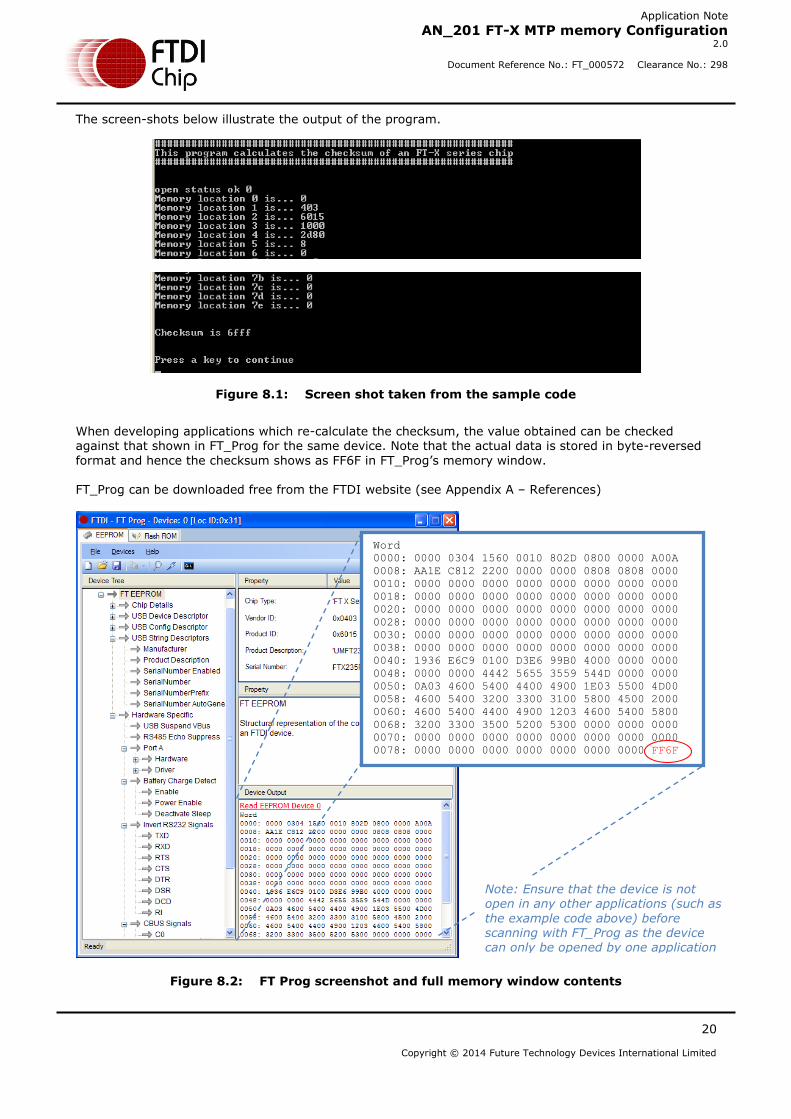
The screen-shots below illustrate the output of the program.
Figure 8.1: Screen shot taken from the sample code
When developing applications which re-calculate the checksum, the value obtained can be checked against that shown in FT_Prog for the same device. Note that the actual data is stored in byte-reversed
format and hence the checksum shows as FF6F in FT_Prog’s memory window. FT_Prog can be downloaded free from the FTDI website (see Appendix A – References)
Figure 8.2: FT Prog screenshot and full memory window contents
Word
0000: 0000 0304 1560 0010 802D 0800 0000 A00A
0008: AA1E C812 2200 0000 0000 0808 0808 0000
0010: 0000 0000 0000 0000 0000 0000 0000 0000
0018: 0000 0000 0000 0000 0000 0000 0000 0000
0020: 0000 0000 0000 0000 0000 0000 0000 0000
0028: 0000 0000 0000 0000 0000 0000 0000 0000
0030: 0000 0000 0000 0000 0000 0000 0000 0000
0038: 0000 0000 0000 0000 0000 0000 0000 0000
0040: 1936 E6C9 0100 D3E6 99B0 4000 0000 0000
0048: 0000 0000 4442 5655 3559 544D 0000 0000
0050: 0A03 4600 5400 4400 4900 1E03 5500 4D00
0058: 4600 5400 3200 3300 3100 5800 4500 2000
0060: 4600 5400 4400 4900 1203 4600 5400 5800
0068: 3200 3300 3500 5200 5300 0000 0000 0000
0070: 0000 0000 0000 0000 0000 0000 0000 0000
0078: 0000 0000 0000 0000 0000 0000 0000 FF6F
Note: Ensure that the device is not open in any other applications (such as
the example code above) before scanning with FT_Prog as the device can only be opened by one application at a time.
21
Copyright © 2014 Future Technology Devices International Limited
Application Note
AN_201 FT-X MTP memory Configuration 2.0
Document Reference No.: FT_000572 Clearance No.: 298
9 Contact Information
Head Office – Glasgow, UK Future Technology Devices International Limited Unit 1, 2 Seaward Place, Centurion Business Park Glasgow G41 1HH United Kingdom Tel: +44 (0) 141 429 2777 Fax: +44 (0) 141 429 2758 E-mail (Sales) [email protected] E-mail (Support) [email protected] E-mail (General Enquiries) [email protected]
Branch Office – Taipei, Taiwan Future Technology Devices International Limited (Taiwan) 2F, No. 516, Sec. 1, NeiHu Road Taipei 114 Taiwan , R.O.C. Tel: +886 (0) 2 8791 3570 Fax: +886 (0) 2 8791 3576 E-mail (Sales) [email protected] E-mail (Support) [email protected] E-mail (General Enquiries) [email protected]
Branch Office – Tigard, Oregon, USA Future Technology Devices International Limited (USA) 7130 SW Fir Loop Tigard, OR 97223-8160 USA Tel: +1 (503) 547 0988 Fax: +1 (503) 547 0987 E-Mail (Sales) [email protected] E-Mail (Support) [email protected] E-Mail (General Enquiries) [email protected]
Branch Office – Shanghai, China Future Technology Devices International Limited (China) Room 1103, No. 666 West Huaihai Road, Shanghai, 200052 China Tel: +86 21 62351596 Fax: +86 21 62351595 E-mail (Sales) [email protected] E-mail (Support) [email protected] E-mail (General Enquiries) [email protected]
Web Site http://ftdichip.com
System and equipment manufacturers and designers are responsible to ensure that their systems, and any Future Technology Devices
International Ltd (FTDI) devices incorporated in their systems, meet all applicable safety, regulatory and system-level performance
requirements. All application-related information in this document (including application descriptions, suggested FTDI devices and other
materials) is provided for reference only. While FTDI has taken care to assure it is accurate, this information is subject to customer
confirmation, and FTDI disclaims all liability for system designs and for any applications assistance provided by FTDI. Use of FTDI devices in life support and/or safety applications is entirely at the user’s risk, and the user agrees to defend, indemnify and hold
harmless FTDI from any and all damages, claims, suits or expense resulting from such use. This document is subject to change without
notice. No freedom to use patents or other intellectual property rights is implied by the publication of this document. Neither the whole
nor any part of the information contained in, or the product described in this document, may be adapted or reproduced in any material
or electronic form without the prior written consent of the copyright holder. Future Technology Devices International Ltd, Unit 1, 2
Seaward Place, Centurion Business Park, Glasgow G41 1HH, United Kingdom. Scotland Registered Company Number: SC136640
22
Copyright © 2014 Future Technology Devices International Limited
Application Note
AN_201 FT-X MTP memory Configuration 2.0
Document Reference No.: FT_000572 Clearance No.: 298
Appendix A – References
Document References
[1] FT_Prog utility for programming the MTP over USB
http://www.ftdichip.com/Support/Utilities.htm#FT_Prog
[2] D2xx Programmers Guide
http://www.ftdichip.com/Support/Documents/ProgramGuides/D2XX_Programmer's_Guide(FT_000071).pdf
[3] FT-X family product page
http://www.ftdichip.com/FT-X.htm
Acronyms and Abbreviations
Terms Description
CBUS Configurable I/O pins on FTDI devices
FT1248 FTDI Dynamic Parallel/Serial bus (between 1 and 8 bits wide)
I2C Inter-Integrated Circuit bus
MTP Multi-Time Programmable memory
PID Product ID (for example, the FT-X devices use 0x6015 by default)
USB Universal Serial Bus
VID Vendor ID (for example, FTDI’s Vendor ID is 0x0403)
23
Copyright © 2014 Future Technology Devices International Limited
Application Note
AN_201 FT-X MTP memory Configuration 2.0
Document Reference No.: FT_000572 Clearance No.: 298
Appendix B – List of Tables & Figures
List of Tables
Table 7.1: Misc Config Bit Description ...................................................................... 12
Table 7.2: USB VID ................................................................................................... 12
Table 7.3: USB PID ................................................................................................... 12
Table 7.4 BCD Release Number ................................................................................ 12
Table 7.5: Max power and USB Configuration Options .............................................. 12
Table 7.6: Device & Peripheral Control ..................................................................... 13
Table 7.7: IO Control ................................................................................................ 14
Table 7.8: Manufacturer String Descriptor ................................................................ 14
Table 7.9: Product String Descriptor ........................................................................ 14
Table 7.10: Serial Number String Descriptor ............................................................ 14
Table 7.11: I2C Slave Address .................................................................................. 15
Table 7.12: I2C Device ID ......................................................................................... 15
Table 7.13: I2C Device ID ......................................................................................... 15
Table 7.14: CBUS[1:0] Control ................................................................................. 15
Table 7.15: CBUS[3:2] Control ................................................................................. 15
Table 7.16: CBUS[5:4] Control ................................................................................. 15
Table 7.17: CBUS[6] Mux Control ............................................................................. 16
Table 7.18: CBUS Multiplexer Select ......................................................................... 17
List of Figures
Figure 3.1: Simplified memory map for the FT-X ..................................................... 6
Figure 3.2: Memory map for the FT-X ...................................................................... 7
Figure 8.1: Screen shot taken from the sample code ............................................. 20
Figure 8.2: FT Prog screenshot and full memory window contents ........................ 20
24
Copyright © 2014 Future Technology Devices International Limited
Application Note
AN_201 FT-X MTP memory Configuration 2.0
Document Reference No.: FT_000572 Clearance No.: 298
Appendix C – Revision History
Document Title: AN_201 FT-X MTP memory Configuration Document Reference No.: FT_000572 Clearance No.: 298 Product Page: http://www.ftdichip.com/FT-X.htm Document Feedback: Send Feedback
Revision Changes Date
1.0 Initial Release 21/06/12
2.0 Updated Figure 3.2 to outline the correct area of memory which is checksummed.
Corrected address range used in Section 8 checksum calculation.
Removed references to FT1248 as programming MTP over
FT1248 not currently supported.
Added example code in Section 8.1 to show calculation of a checksum
18/12/13