Embed Size (px)
Citation preview
IEEE 64th ECTC – Orlando, FL, USA May 27–30, 2014
Future packaging and required interposer technologies for
cognitive computing devices
Yasumitsu Orii,Senior Manager of Science & Technology, IBM Research Tokyo
2014 CPMT SeminarLatest Advances in Organic Interposers

2IEEE 64th ECTC – Orlando, FL, USA May 27 – 30, 2014Yasumitsu Orii 2May 27 – 30, 2014
• Computer System for the Era of Big Data
• What is “Cognitive Computer” ?
• Requirement for Cognitive Computing Devices
– Interposer Technologies
– Packaging Technologies
Agenda / Outline / Overview

3IEEE 64th ECTC – Orlando, FL, USA May 27 – 30, 2014Yasumitsu Orii 3May 27 – 30, 2014
• Computer System for the Era of Big Data
• What is “Cognitive Computer” ?
• Requirement for Cognitive Computing Devices
– Interposer Technologies
– Packaging Technologies
Agenda / Outline / Overview

4IEEE 64th ECTC – Orlando, FL, USA May 27 – 30, 2014Yasumitsu Orii 4May 27 – 30, 2014
Info-Plosion
The oceans of data to be produced in the worldThe size of data generated per Day in 2010 is “1ZB”, which is equal to 3.7 trillion years News Paper Data.

5IEEE 64th ECTC – Orlando, FL, USA May 27 – 30, 2014Yasumitsu Orii 5May 27 – 30, 2014
3 40zettabytes zettabytes
2012 2020
Source: IDC Digital Universe
Data volume is increasing !

6IEEE 64th ECTC – Orlando, FL, USA May 27 – 30, 2014Yasumitsu Orii 6May 27 – 30, 2014
Internet of Things

7IEEE 64th ECTC – Orlando, FL, USA May 27 – 30, 2014Yasumitsu Orii 7May 27 – 30, 2014
11 42% %
2005 2020
Ratio of the data generated by sensors
Source: IDC Digital Universe
Big data to be accelerated by IoT

8IEEE 64th ECTC – Orlando, FL, USA May 27 – 30, 2014Yasumitsu Orii 8May 27 – 30, 2014
Capacity of communication Infrastructure exceeds its limit in 2020
Glo
bal D
ata
Volu
me
in E
xaby
tes
Multiple sources: IDC,Cisco
100
90
80
70
60
50
40
30
20
10
Aggr
egat
e U
ncer
tain
ty %
9000
8000
7000
6000
5000
4000
3000
2000
1000
0
2005 2010 2015
Uncertain
Certain
Global Technology Outlook 2012
9IEEE 64th ECTC – Orlando, FL, USA May 27 – 30, 2014Yasumitsu Orii 9May 27 – 30, 2014
• Computer System for the Era of Big Data
• What is “Cognitive Computer” ?
• Requirement for Cognitive Computing Devices
– Interposer Technologies
– Packaging Technologies
Agenda / Outline / Overview

10IEEE 64th ECTC – Orlando, FL, USA May 27 – 30, 2014Yasumitsu Orii 10May 27 – 30, 2014
Cognitive Systems: A new era of computingC
ompu
ter I
ntel
ligen
ce
Time
TabulatingSystems Era
Programmable Systems Era
CognitiveSystems Era
3rd Generation

11IEEE 64th ECTC – Orlando, FL, USA May 27 – 30, 2014Yasumitsu Orii 11May 27 – 30, 2014
IBM Watson Project
Ken Jennings, who won a record 74 consecutive "Jeopardy!" games in 2004-05 Brad Rutter, who is the biggest all-time money winner.
15TB Memory2,880 Processor core200KW
System to backup more rapid and accurate medical diagnosis.
System to check potential coactions between medicines.
System to refer past authority by lawyers and benches.
System for hypothesis scenario and legal compliance in finance sector.
It is expected to apply the technologies for Watson to many applications.

12IEEE 64th ECTC – Orlando, FL, USA May 27 – 30, 2014Yasumitsu Orii 12May 27 – 30, 2014
Computers and the Brain are Different and Complementary
10 Hz, parallel, high fanout
20W
1.2 L
106 neurons/cm2
Integrates memory
3.55 GHz, sequential, linear
200kW
12,000 L
~5,000 connections/cm2
Separates memory

13IEEE 64th ECTC – Orlando, FL, USA May 27 – 30, 2014Yasumitsu Orii 13May 27 – 30, 2014
IBM Creating New Cognitive Technologies
OFF
ON
Crossbar architecture
Power, space, memory, and communication scale with synapses

14IEEE 64th ECTC – Orlando, FL, USA May 27 – 30, 2014Yasumitsu Orii 14May 27 – 30, 2014
Brain-inspired Chip
~1010 synapses/cm2 ~106 neurons/cm2
5x10⁸ transistors/cm2
@500 transistors/neuron
~104 neurons/cortical column
Biological Brain
Electronic BrainMulti-Gbit/secDigital comms
Layered cortical circuits with ~106
neurons/cm2
~1010 intersections/cm2 @ 100 nm pitch
~5x10³ long range axons @ 1 Hz
(Ref. http://archive.hpcwire.com/hpcwire/2011-08-18/ibm_reveals_cognitive_computing_chips.html)

15IEEE 64th ECTC – Orlando, FL, USA May 27 – 30, 2014Yasumitsu Orii 15May 27 – 30, 2014
• Computer System for the Era of Big Data
• What is “Cognitive Computer” ?
• Requirement for Cognitive Computing Devices
– Interposer Technologies
– Packaging Technologies
Agenda / Outline / Overview

16IEEE 64th ECTC – Orlando, FL, USA May 27 – 30, 2014Yasumitsu Orii 16May 27 – 30, 2014
Human’s brain
• Human’s brain: 1011 (100Billion) neurons1015 (1000Trillion) synapses
Wikipedia
1400cm3 (1.4L)
Eye: 1B neurons10T synapses
J. DiCarlo et al., Neuron, 2012

17IEEE 64th ECTC – Orlando, FL, USA May 27 – 30, 2014Yasumitsu Orii 17May 27 – 30, 2014
Brain size of mammals
S. Herculano-Houzel 2009
Mouse’s brain:70M neurons700B synapses
Mouse’s vision (est.):0.7M neurons (~1M)7B synapses (~10B)
Human’s brain:100B neurons1,000T synapses
Human’s vision:1B neurons10T synapses

18IEEE 64th ECTC – Orlando, FL, USA May 27 – 30, 2014Yasumitsu Orii
Package Outline on Implementation
Chained synapse to neuron connection
• Package outline• 4 die stacked with 7mmSQ chips.• Area arrayed 125,000 signal I/Os and same counts of power and ground per chip in 14m
pitch.• 16 die stacks on interposer.• Chained synapse to synapse connection between die stacks.
Information input for neuron
interposer
16 die stacks
• Assumption : Mouse’s eye (synapse=10B, # of neurons=1M)Number of I/O estimation• Tota signal I/O of neurons: 1M x 2 • Total I/O with power & ground: 4M• Layers of RBM: 16 (= number of stacked chip)• Total I/O with power & ground of a stack (4dies)
: 1M x 2 x 2 / 16=250,000
Die size estimation• Total drivers of a stack (4 dies) :125,000• # of driver on a die: 125,000 / 4=31,250• Area of driver (45nm): 25 x 50 =1,250um2
• Area of die: 0.00125 x 31,250 um2
= 39.0625mm2 -> 6.25mm2
19IEEE 64th ECTC – Orlando, FL, USA May 27 – 30, 2014Yasumitsu Orii
0
2
4
6
8
10
12
14
16
18
20
0 0.2 0.4 0.6 0.8 1
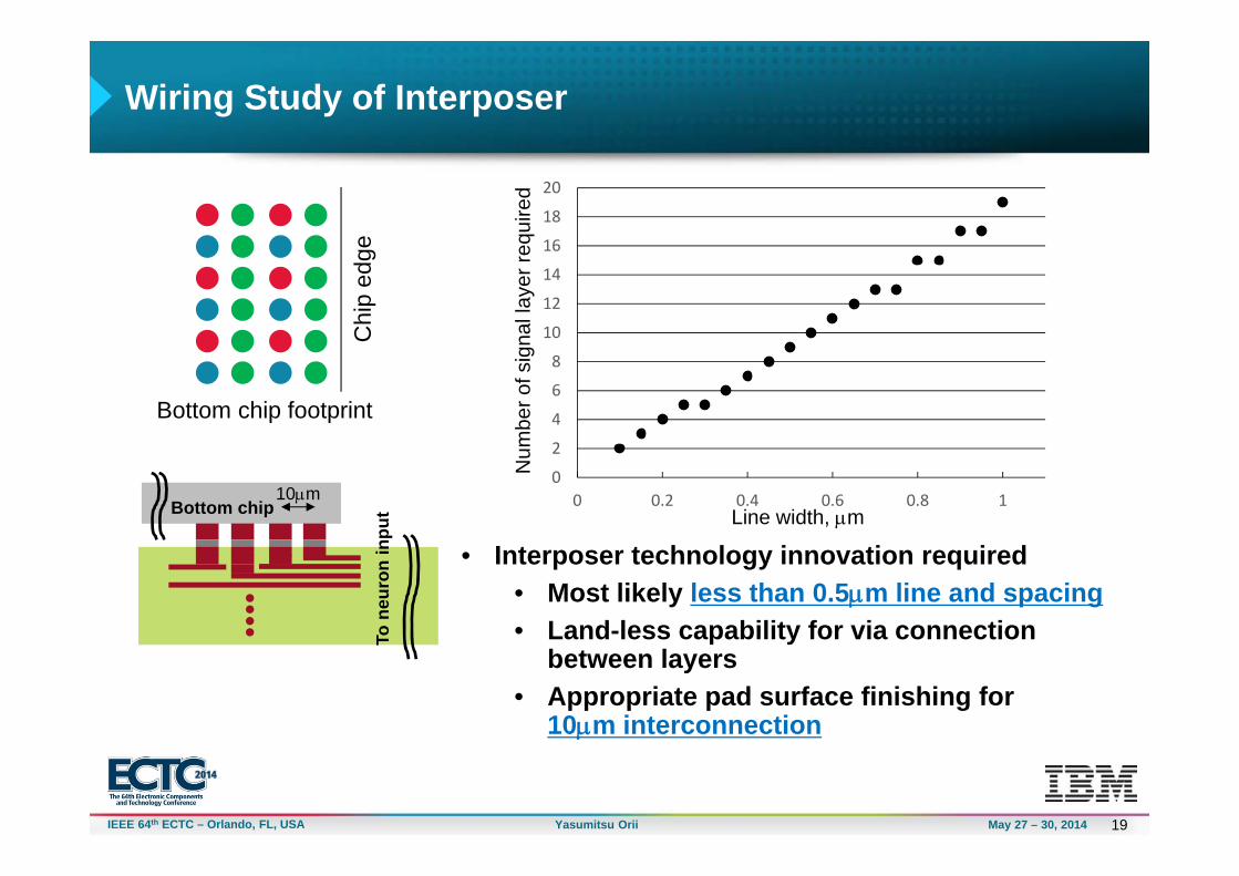
Wiring Study of Interposer
Chi
p ed
ge
10m
To n
euro
n in
put
Bottom chip footprint
Bottom chip Line width, mN
umbe
r of s
igna
l lay
er re
quire
d• Interposer technology innovation required
• Most likely less than 0.5m line and spacing• Land-less capability for via connection
between layers• Appropriate pad surface finishing for
10m interconnection
20IEEE 64th ECTC – Orlando, FL, USA May 27 – 30, 2014Yasumitsu Orii 20May 27 – 30, 2014
• Computer System for the Era of Big Data
• What is “Cognitive Computer” ?
• Requirement for Cognitive Computing Devices
– Interposer Technologies
– Packaging Technologies
Agenda / Outline / Overview

21IEEE 64th ECTC – Orlando, FL, USA May 27 – 30, 2014Yasumitsu Orii 21May 27 – 30, 2014
10micron pitch interconnection
Solder bump: 5m Ni/Au pad: 6m
Al wiring
Post:3mt
(Cu. Ni)
SnAg:3mtNi:3mt /Au:0.1mt
Solder bump: 5m Ni/Au pad: 6m
Al wiring
Post:3mt
(Cu. Ni)
SnAg:3mtNi:3mt /Au:0.1mt
Substrate : 10mmx10mm
4X4 10 m-pitch cluster bumps
Chip7mmx7mm
- Wiring on chip/substrate
- Bump/Pad structure
30X30 100 m-pitch cluster array 10 m pitch SnAg bump
10 m pitch Ni/Au pad
IMCs
IMCs
22IEEE 64th ECTC – Orlando, FL, USA May 27 – 30, 2014Yasumitsu Orii 22May 27 – 30, 2014
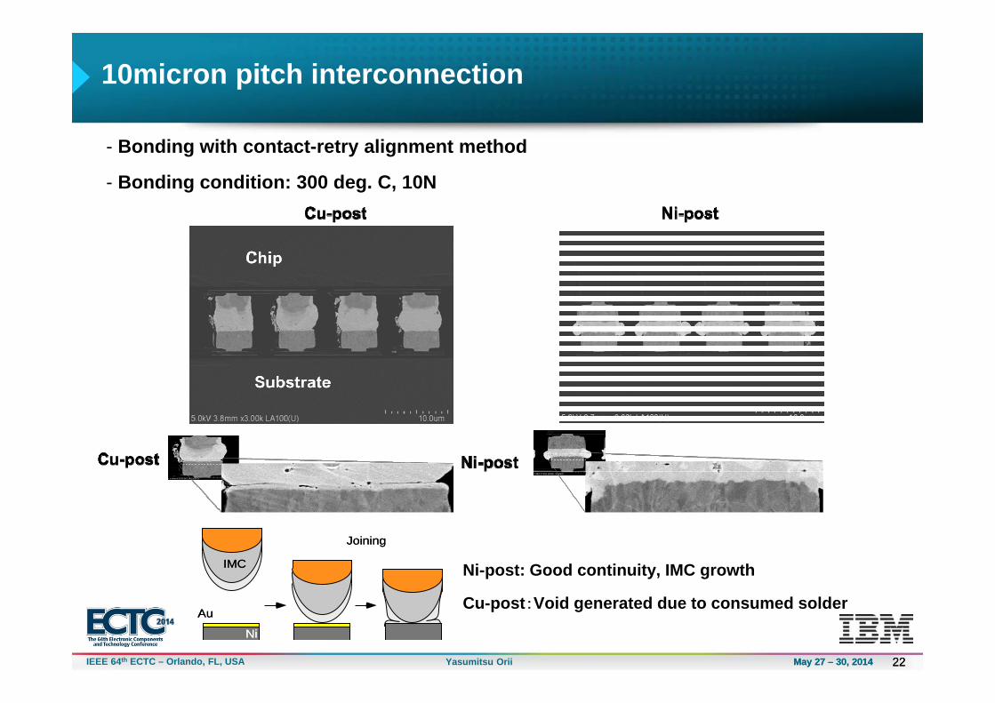
- Bonding with contact-retry alignment method
- Bonding condition: 300 deg. C, 10N
Joining
IMC
Ni
Au
Joining
IMC
Ni
Au
Joining
IMC
Ni
Au
Ni-post: Good continuity, IMC growth
Cu-post:Void generated due to consumed solder
10micron pitch interconnection

23IEEE 64th ECTC – Orlando, FL, USA May 27 – 30, 2014Yasumitsu Orii 23May 27 – 30, 2014
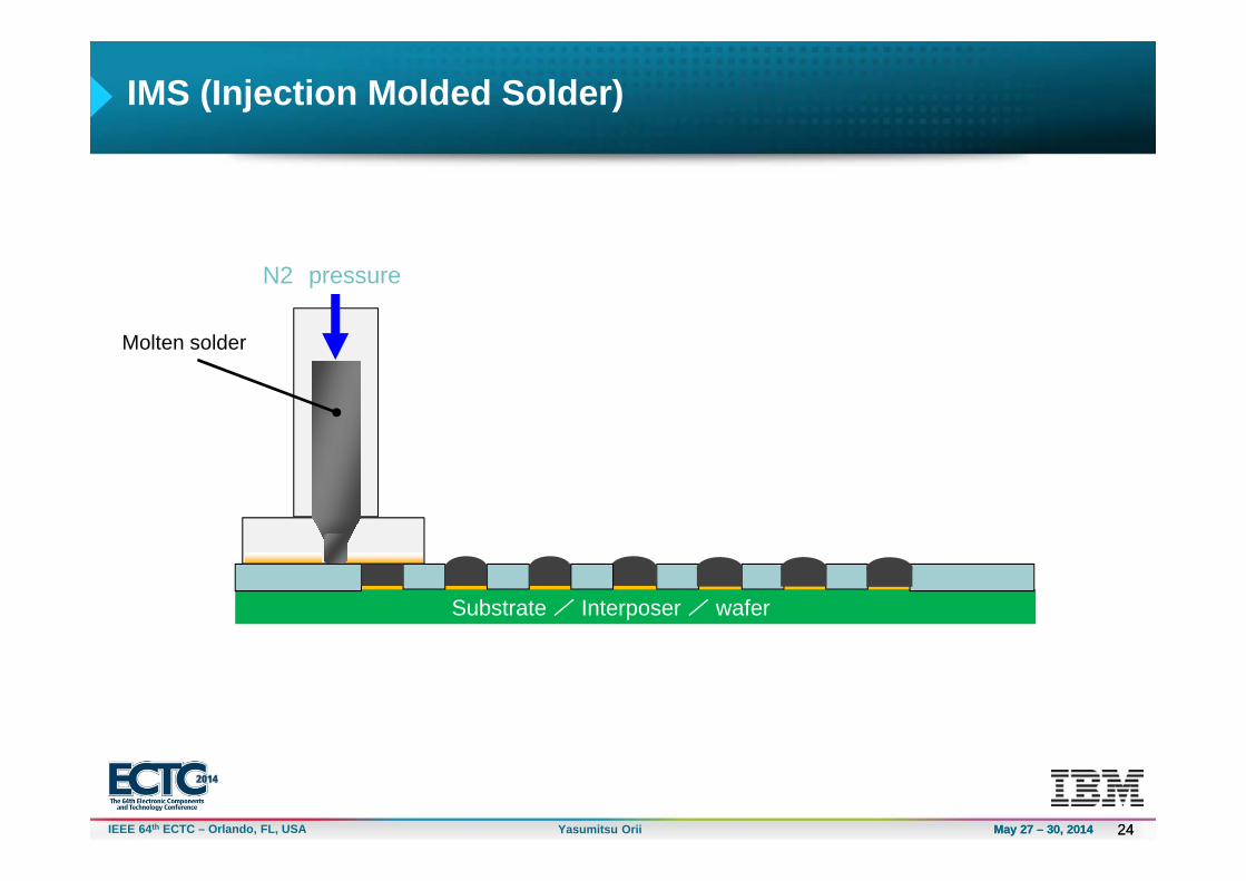
IMS (Injection Molded Solder) technology
Very simple process Green process
• No flux, No formic acid• Minimum solder waste
Pure solder injection• Higher solder volume• Extendible to very fine pitch• Solder alloy flexibility
One pass for multiple solder sizes
Solder Paste (Solder powder + Flux)
Reflow + Cleaning
Squeegee
Metalmask
Substrate
- Solder Paste Printing Method -
IMS head
Mask
Molten Solder
Interposer
- Molten Solder Injection Method -
reference
24IEEE 64th ECTC – Orlando, FL, USA May 27 – 30, 2014Yasumitsu Orii 24May 27 – 30, 2014
IMS (Injection Molded Solder)
Substrate / Interposer / wafer
Molten solder
N2 pressure

25IEEE 64th ECTC – Orlando, FL, USA May 27 – 30, 2014Yasumitsu Orii 25May 27 – 30, 2014
Wafer IMS technology : Demonstration with 8’ wafer
50um
50um diameter
50um
75um diameter
Wafer IMS demonstration with various opening size in 8 inch wafer !!!
solder bump solder bump
Demonstrated Wafer IMS bumping with 8 inch wafer

26IEEE 64th ECTC – Orlando, FL, USA May 27 – 30, 2014Yasumitsu Orii 26May 27 – 30, 2014
Experimental Results of IMS TechnologyB
efor
eSt
rippi
ngA
fter
Strip
ping
30m 40m 50m 75m 100m
After IMS After Stripping After Cu seed etch
50m
30m
8inch wafer
No residue was confirmed through stripping and Cu seed etchingThe process was confirmed for several bump diameters

27IEEE 64th ECTC – Orlando, FL, USA May 27 – 30, 2014Yasumitsu Orii 27May 27 – 30, 2014
A Future led by Cognitive technology
Ref. IEICEVol.94,No.8,2011
Terminal devices responsible for low-end cognitive processing and delivery to data center, to avoid information explosion
Terminal devices enable cognitive processing.Workload is balanced b/w data center and terminals.
Data center responsible for advanced cognitive processing using accumulated valuable information

28IEEE 64th ECTC – Orlando, FL, USA May 27 – 30, 2014Yasumitsu Orii 28May 27 – 30, 2014
Mission for IBM Research Tokyo
Metal Interconnect
Optical interconnect
Wireless interconnect
Current computer Future computer
Toyosu
Shin-Kawasaki
Universities
PartnersCognitive & Bio-inspiredvon Neumann architecture
System technology research
Element technology research
System technology research and element technology research for new era computing will be performed under collaboration among universities and partners.

29IEEE 64th ECTC – Orlando, FL, USA May 27 – 30, 2014Yasumitsu Orii
Thank you for your attention !


![Color Panel Memory Test [CPMT]](https://img.pdfslide.us/doc/110x75/549ab475b4795938098b4593/color-panel-memory-test-cpmt.jpg)