Embed Size (px)
Citation preview

Volume 1 Issue 7
AuGusT 2007
The newsleTTer for The ThermAl mAnAGemenT of elecTronIcs
Micro TECs for Spot Cooling of High Power Devices
fuTure coolInG
PublIshed by AdVAnced ThermAl soluTIons, Inc. | 89-27 Access roAd norwood, mA 02062 | T: 781.769.2800 www.qATs.com PAGe 1
Introduction As component packages shrink, and power densities increase with higher operating frequencies, challenges to thermal engineers are greater than ever for cooling such devices. One thermal management technique of growing interest is to cool localized areas of high heat flux that create so called “hot-spots” or areas of high-temperature on die surfaces, as shown in Figure 1.
Figure 1. Component with Hot Spot as Dem-onstrated by Liquid Crystal Thermography.
Hot spot temperatures can be 5 to 30K higher than other areas of the micropro-cessor, and their temperature differenc-es can surpass 100K for optoelectronic components [1].
A typical thermal solution would be to design a heat sink to cool the entire component, i.e. both the hot-spot and surrounding areas of the chip. But this blunt force approach is very inefficient because the heat sink will cool both the critical areas (hot spots) and the non-critical (lower temperature) areas of the chip. This results in a greater than necessary heat load to the system. One possible approach is to use a micro TEC (small thermoelectric coolers) at the source of the hot spot to remove the heat only in the critical areas as shown in Figure 2. This will reduce the hot spot temperature and may eliminate the thermal stress on the device.
In this issue:
Future Cooling
Thermal Minutes
1
5
Thermal Analysis
Who We Are
8
Thermal Fundamentals12
Cooling News17
18
Figure 2. Typical Application for micro TEC Cooler [1].
PublIshed by AdVAnced ThermAl soluTIons, Inc. | 89-27 Access roAd norwood, mA 02062 | T: 781.769.2800 www.qATs.com PAGe 2
fuTure coolInG
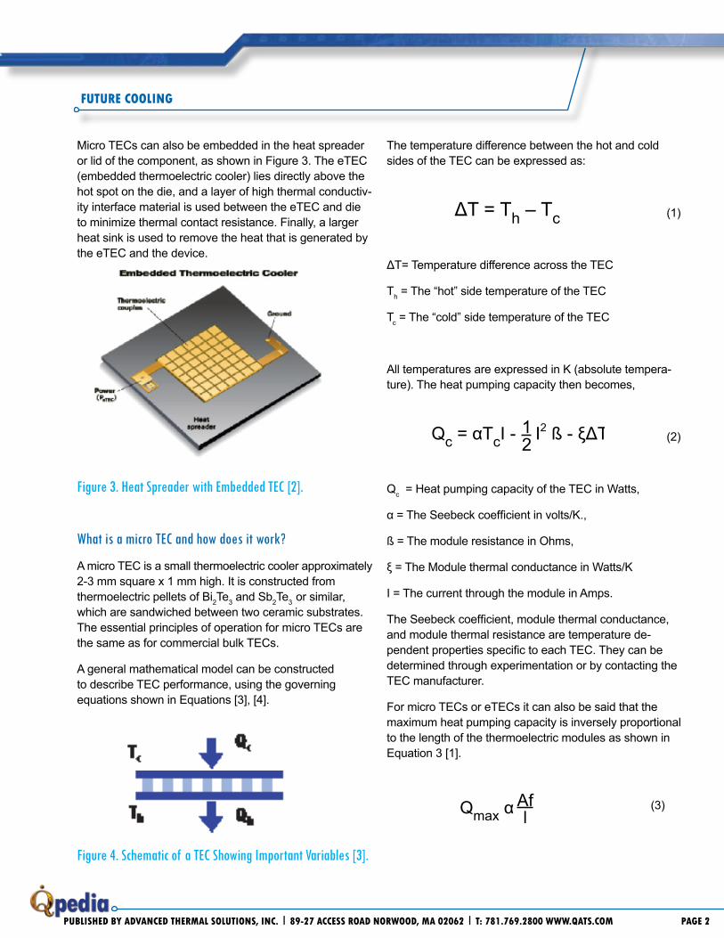
Micro TECs can also be embedded in the heat spreader or lid of the component, as shown in Figure 3. The eTEC (embedded thermoelectric cooler) lies directly above the hot spot on the die, and a layer of high thermal conductiv-ity interface material is used between the eTEC and die to minimize thermal contact resistance. Finally, a larger heat sink is used to remove the heat that is generated by the eTEC and the device.
Figure 3. Heat Spreader with Embedded TEC [2].
What is a micro TEC and how does it work?
A micro TEC is a small thermoelectric cooler approximately 2-3 mm square x 1 mm high. It is constructed from thermoelectric pellets of Bi2Te3 and Sb2Te3 or similar, which are sandwiched between two ceramic substrates. The essential principles of operation for micro TECs are the same as for commercial bulk TECs.
A general mathematical model can be constructed to describe TEC performance, using the governing equations shown in Equations [3], [4].
Figure 4. Schematic of a TEC Showing Important Variables [3].
The temperature difference between the hot and cold sides of the TEC can be expressed as:
(1)
ΔT= Temperature difference across the TEC
Th = The “hot” side temperature of the TEC
Tc = The “cold” side temperature of the TEC
All temperatures are expressed in K (absolute tempera-ture). The heat pumping capacity then becomes,
(2)
Qc = Heat pumping capacity of the TEC in Watts,
α = The Seebeck coefficient in volts/K.,
ß = The module resistance in Ohms,
ξ = The Module thermal conductance in Watts/K
I = The current through the module in Amps.
The Seebeck coefficient, module thermal conductance, and module thermal resistance are temperature de-pendent properties specific to each TEC. They can be determined through experimentation or by contacting the TEC manufacturer.
For micro TECs or eTECs it can also be said that the maximum heat pumping capacity is inversely proportional to the length of the thermoelectric modules as shown in Equation 3 [1].
(3)
ΔT = Th – Tc Qc = αTcI - I
2 ß - ξΔT
Qmax α
COP =
ΔTTECOP>Qc(RSPREAD + RTIM + RSINK)
12
Afl
QlVΔT = Th – Tc
Qc = αTcI - I
2 ß - ξΔT
Qmax α
COP =
ΔTTECOP>Qc(RSPREAD + RTIM + RSINK)
12
Afl
QlV
ΔT = Th – Tc Qc = αTcI - I
2 ß - ξΔT
Qmax α
COP =
ΔTTECOP>Qc(RSPREAD + RTIM + RSINK)
12
Afl
QlV
PublIshed by AdVAnced ThermAl soluTIons, Inc. | 89-27 Access roAd norwood, mA 02062 | T: 781.769.2800 www.qATs.com PAGe �
fuTure coolInG
A = Plan area of the thermoelectric cooler
f = Fraction of area covered by thermoelectric elements
l = Length of the thermoelectric elements.
If the length of the elements is decreased, the heat pumping capacity will increase. Thus, the thinner the eTEC, the better the performance.
Generally speaking, the efficiency of micro TECs (or bulk TECs for that matter) is described by the coefficient of performance equation (Equation 4).
(4)
Q = Heat removed by the TEC in Watts
I = Input current in Amps
V = Input voltage in Volts
IV = Input power
Clearly, the higher the COP the better, as the result is greater heat pumping capacity with respect to input power.
Finally, when deciding if and when to use a micro TEC, the central issue is to determine if adding one will result in improved performance over just the heat sink alone. This condition is true if the inequality below is satisfied (see Equation 5) [1].
(5)
∆TTE = Temperature difference across the TEC
COP = Coefficient of performance (defined in Equation 4)
Qc = Required heat pumping capacity (cold side of TEC)
RSPREAD = Thermal resistance due to spreading
RTIM = Thermal resistance due to thermal interface material
RSINK = Thermal resistance from heat sink
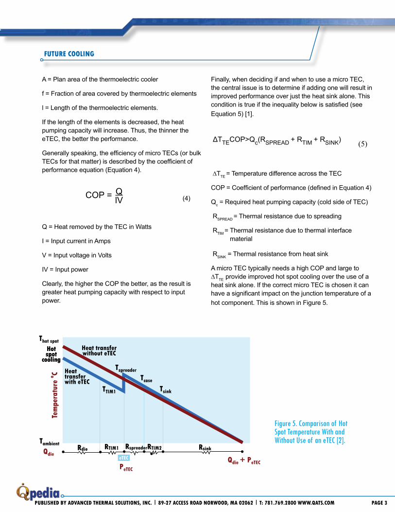
A micro TEC typically needs a high COP and large to ∆TTE provide improved hot spot cooling over the use of a heat sink alone. If the correct micro TEC is chosen it can have a significant impact on the junction temperature of a hot component. This is shown in Figure 5.
ΔT = Th – Tc Qc = αTcI - I
2 ß - ξΔT
Qmax α
COP =
ΔTTECOP>Qc(RSPREAD + RTIM + RSINK)
12
Afl
QlV
ΔT = Th – Tc Qc = αTcI - I
2 ß - ξΔT
Qmax α
COP =
ΔTTECOP>Qc(RSPREAD + RTIM + RSINK)
12
Afl
QlV
Qc
Qh
Tc
Th
HEAT SINKTIM2
HEAT SPREADERTIM1
ICSUBSTRATE
Thot spot
Hotspot
cooling
Hotspot
cooling
Heat transfer without eTEC
Tspreader
Tcase
Tsink
Heattransfer with eTEC
TTIM1
Tambient
QdieRdie RTIM1 RspreaderRTIM2 Rsink
PeTEC
Qdie + PeTEC
Tem
pera
ture
o C
eTEC
Figure 5. Comparison of Hot Spot Temperature With and Without Use of an eTEC [2].

PublIshed by AdVAnced ThermAl soluTIons, Inc. | 89-27 Access roAd norwood, mA 02062 | T: 781.769.2800 www.qATs.com PAGe �
fuTure coolInG
Conclusion The use of micro TECs offer an attractive solution to the thermal engineer who needs to address the issue of cool-ing component hot spots. Micro TECs can be seamlessly integrated into component packages and heat spreaders to focus cooling where it is needed most. The result can be an effective thermal solution that allows for improved thermal management of hot devices [1].
When designing with micro TECs one should select devices with high COP and large ∆TTE capability. The micro TECs should be as thin as possible as this will allow for the best thermal performance and highest level of responsiveness. From a practical standpoint, the technology exists to fabricate TECs directly on to the die or component heat spreader using microfabrication tech-niques such as thick film electroplating, vacuum deposi-tion, and chemical vapor deposition. These processes result in extremely thin TECs with high performance [1].
Finally, while the best micro TECs are now made from Bi2Te3 and Sb2Te3 the world of new materials is ever expanding. It is reasonable to expect that the micro TECs of the future will be better and faster than those of today.
References:
1. Koester, D., Venkatasubramanian, R., Conner, B., Snyder, G., Embedded Thermoelectric Coolers for Semiconductor Hot Spot Cooling, IEEE 2006.
2. Conner, B., Hot Spot Cooling, Semiconductor International, February 2007.
3. Thermoelectric Technical Reference, FerroTec Corporation, 2001-2006.
4. Godfrey, S., An Introduction to Thermoelectric Coolers, Melcor Corporation, Electronics Cooling, September 1996.
ATS has just released its new catalog of over 380 Heat Sink solutions for cooling BGAs, Freescale single and dual-core processors, a wide variety of ASICs, and other components. The catalog also includes custom cooling solutions for linear LED lighting applications.
Products in the new catalog are available exclusively through Digi-Key, the global electronic components distributor, and include heat sinks with ATS’ maxiFLOW™ flared fin technology for maximum convection cooling and the maxiGRIP™ system for safe and secure heat sink attachment to flip chips, BGAs, and other component types.
GET YoUR CopY oF ATS’ NEW HEAT SINK CATALoG
To request your copy or ATS’ new Heat Sink Catalog, please visit www.qats.com or call 781-769-2800. You can also visit www.digikey.com or call 1-800-DIGI-KEY to check inventory, place an order or, to find additional information on ATS’ high performance cooling solutions.

PublIshed by AdVAnced ThermAl soluTIons, Inc. | 89-27 Access roAd norwood, mA 02062 | T: 781.769.2800 www.qATs.com PAGe 5
ThermAl mInuTes
Many Qpedia articles discuss ways to sustain effective cooling as components get smaller and their power levels rise. Yet, continuing advances in packaging and die technology are increasing the demands for thermal management.
One result is pressure on engineers to replace standard heat sinks with optimized, higher performance designs. Optimized heat sinks offer more performance with less weight, in a smaller spatial volume, than an off the shelf designs. This allows the use of higher frequency compo-nents, and ideally leads to higher performing end prod-ucts. Despite these benefits, because of PCB layout and system configuration, there is no one simple method for optimizing heat sink geometry to guarantee increased performance. One such a way to optimize the heat sink is optimizing the air flow to the heat sink by relaying out the components for optimal flow, and/or optimizing the heat sink design to minimize pressure drop in a PCB.
Effect of Air Velocity in Heat Sink Design Heat sink optimization starts with the basic equation, Newton’s cooling law, for convection heat transfer.
Q = h A ∆T
Q = Rate of heat transfer
h = Convection heat transfer coefficient
A = Convective heat transfer surface area
∆T = Temperature differential
The objective, of course, is to increase Q, the rate of heat
transfer from the heat sink to the environment. At the same time, the component temperature gradient, junction to case, and case to package edge, must be minimized so it doesn’t exceed the manufacturer’s recommended temperature. This leaves the heat transfer coefficient and the convective surface area as the two parameters that must be optimized.
Of these two factors, surface area is the most straight-forward and the easiest place to begin when designing a heat sink. Unfortunately, surface area and the heat transfer coefficient are intrinsically linked and become more prevalent in electronics cooling situations as they must be optimized simultaneously. A proper optimiza-tion must balance the total surface area with a high heat transfer coefficient to provide the best possible thermal performance.
How are the two parameters linked in heat sink design? The answer is pressure drop and its effect on air velocity through the heat sink. The majority of air flow configu-rations in the electronics industry are not ducted. This means that the heat sink experiences bypass flow condi-tions, where the flow can go around the heat sink in addi-tion to through the fin field, i.e. path of least resistance. In ducted flows only the fan performance curve is affected by the pressure drop of the heat sink. In unducted flow the heat sink’s pressure drop also causes air to bypass the sink, which further reduces the effective flow rate through the fin field. In this article we assume a simplified relationship between air velocity and the average heat transfer coefficient. Advanced methods for increasing the heat transfer coefficient by modifying heat sink design geometry are subjects of future articles.
The Effect of Compact PCB Layout on Themal Management
As shown in Figure 1, the lowest thermal resistance is found when the heat sink surface area and the pressure drop are correctly balanced. For example, in the 1 m/s case, a heat sink with 8 fins does not provide enough surface area for optimal cooling, while a 20 fin heat sink is very dense and has a large pressure drop across its length. Neither of these heat sinks is well suited for a 1 m/s bypass flow condition. For this case, the optimal heat sink has 14 fins, as shown in Figure 1.
Figure 1. optimal Fin Quantity as a Function of Velocity.
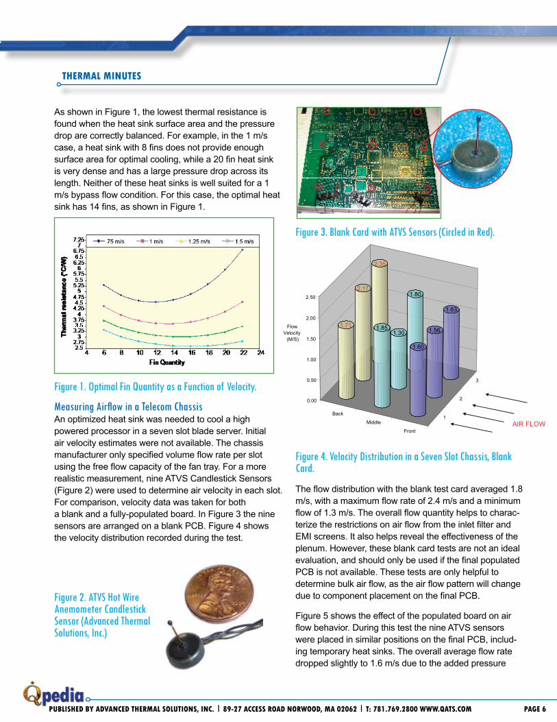
Measuring Airflow in a Telecom Chassis An optimized heat sink was needed to cool a high powered processor in a seven slot blade server. Initial air velocity estimates were not available. The chassis manufacturer only specified volume flow rate per slot using the free flow capacity of the fan tray. For a more realistic measurement, nine ATVS Candlestick Sensors (Figure 2) were used to determine air velocity in each slot. For comparison, velocity data was taken for both a blank and a fully-populated board. In Figure 3 the nine sensors are arranged on a blank PCB. Figure 4 shows the velocity distribution recorded during the test.
Figure 2. ATVS Hot Wire Anemometer Candlestick Sensor (Advanced Thermal Solutions, Inc.)
Figure 3. Blank Card with ATVS Sensors (Circled in Red).
Figure 4. Velocity Distribution in a Seven Slot Chassis, Blank Card.
The flow distribution with the blank test card averaged 1.8 m/s, with a maximum flow rate of 2.4 m/s and a minimum flow of 1.3 m/s. The overall flow quantity helps to charac-terize the restrictions on air flow from the inlet filter and EMI screens. It also helps reveal the effectiveness of the plenum. However, these blank card tests are not an ideal evaluation, and should only be used if the final populated PCB is not available. These tests are only helpful to determine bulk air flow, as the air flow pattern will change due to component placement on the final PCB.
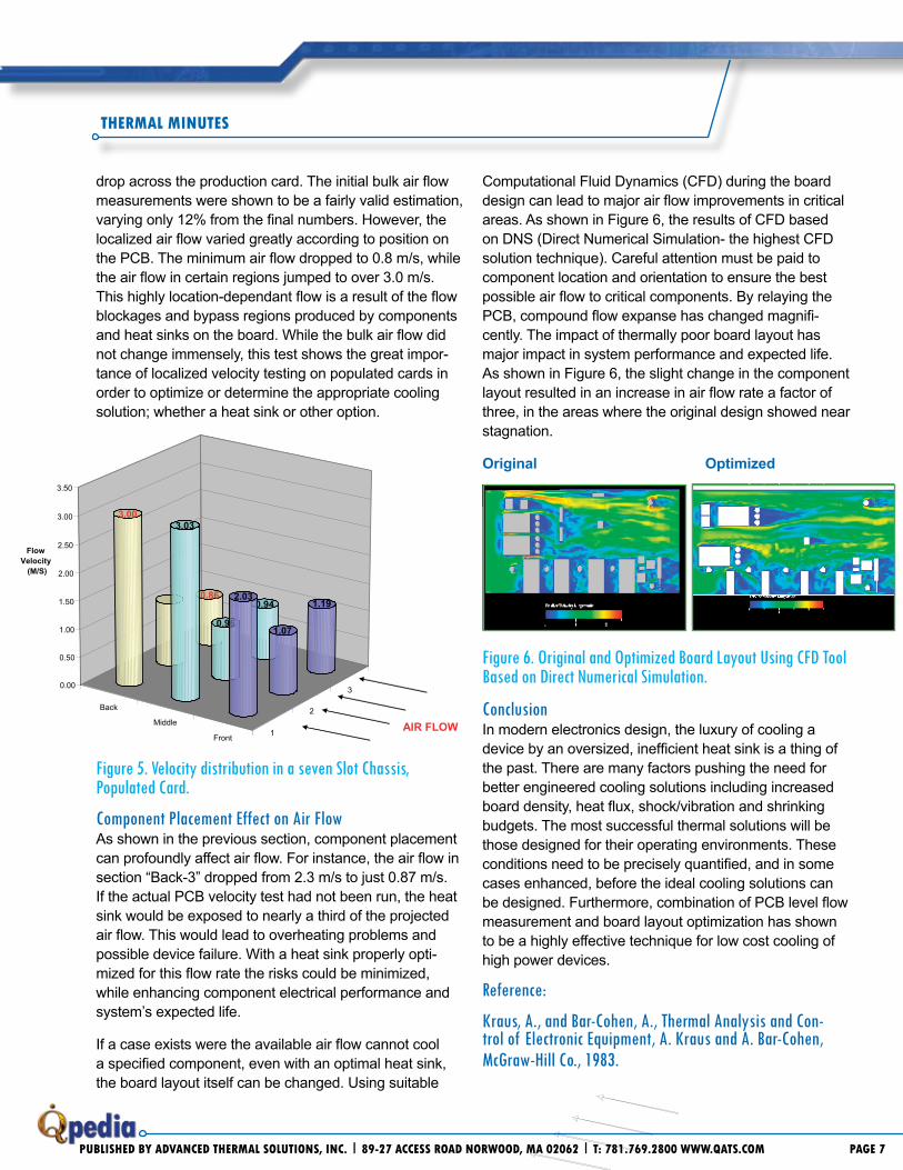
Figure 5 shows the effect of the populated board on air flow behavior. During this test the nine ATVS sensors were placed in similar positions on the final PCB, includ-ing temporary heat sinks. The overall average flow rate dropped slightly to 1.6 m/s due to the added pressure
PublIshed by AdVAnced ThermAl soluTIons, Inc. | 89-27 Access roAd norwood, mA 02062 | T: 781.769.2800 www.qATs.com PAGe 6
ThermAl mInuTes
Heatsink Thermal Resistance as a Function of Air Velocity and Fin Quantity
2.500
2.750
3.000
3.250
3.500
3.750
4.000
4.250
4.500
4.750
4 6 8 10 12 14 16 18 20 22 24Fin Quantity
Ther
mal
resi
stan
ce(°
C/W
)
200 LFM 250 LFM 300 LFM
1
2
3
Front
Middle
Back
2.35
2.17
1.71
1.80
1.301.85
1.63
1.56
1.60
0.00
0.50
1.00
1.50
2.00
2.50
FlowVelocity
(M/S)
AIR FLOW
1
2
3
Front
Middle
Back
0.86
3.00
0.94
0.96
3.03
1.19
1.07
2.03
0.00
0.50
1.00
1.50
2.00
2.50
3.00
3.50
FlowVelocity
(M/S)
AIR FLOW
PublIshed by AdVAnced ThermAl soluTIons, Inc. | 89-27 Access roAd norwood, mA 02062 | T: 781.769.2800 www.qATs.com PAGe 7
ThermAl mInuTes
drop across the production card. The initial bulk air flow measurements were shown to be a fairly valid estimation, varying only 12% from the final numbers. However, the localized air flow varied greatly according to position on the PCB. The minimum air flow dropped to 0.8 m/s, while the air flow in certain regions jumped to over 3.0 m/s. This highly location-dependant flow is a result of the flow blockages and bypass regions produced by components and heat sinks on the board. While the bulk air flow did not change immensely, this test shows the great impor-tance of localized velocity testing on populated cards in order to optimize or determine the appropriate cooling solution; whether a heat sink or other option.
Figure 5. Velocity distribution in a seven Slot Chassis, populated Card.
Component placement Effect on Air Flow As shown in the previous section, component placement can profoundly affect air flow. For instance, the air flow in section “Back-3” dropped from 2.3 m/s to just 0.87 m/s. If the actual PCB velocity test had not been run, the heat sink would be exposed to nearly a third of the projected air flow. This would lead to overheating problems and possible device failure. With a heat sink properly opti-mized for this flow rate the risks could be minimized, while enhancing component electrical performance and system’s expected life.
If a case exists were the available air flow cannot cool a specified component, even with an optimal heat sink, the board layout itself can be changed. Using suitable
Computational Fluid Dynamics (CFD) during the board design can lead to major air flow improvements in critical areas. As shown in Figure 6, the results of CFD based on DNS (Direct Numerical Simulation- the highest CFD solution technique). Careful attention must be paid to component location and orientation to ensure the best possible air flow to critical components. By relaying the PCB, compound flow expanse has changed magnifi-cently. The impact of thermally poor board layout has major impact in system performance and expected life. As shown in Figure 6, the slight change in the component layout resulted in an increase in air flow rate a factor of three, in the areas where the original design showed near stagnation.
Original Optimized
Figure 6. original and optimized Board Layout Using CFD Tool Based on Direct Numerical Simulation.
Conclusion In modern electronics design, the luxury of cooling a device by an oversized, inefficient heat sink is a thing of the past. There are many factors pushing the need for better engineered cooling solutions including increased board density, heat flux, shock/vibration and shrinking budgets. The most successful thermal solutions will be those designed for their operating environments. These conditions need to be precisely quantified, and in some cases enhanced, before the ideal cooling solutions can be designed. Furthermore, combination of PCB level flow measurement and board layout optimization has shown to be a highly effective technique for low cost cooling of high power devices.
Reference:
Kraus, A., and Bar-Cohen, A., Thermal Analysis and Con-trol of Electronic Equipment, A. Kraus and A. Bar-Cohen, McGraw-Hill Co., 1983.
Heatsink Thermal Resistance as a Function of Air Velocity and Fin Quantity
2.500
2.750
3.000
3.250
3.500
3.750
4.000
4.250
4.500
4.750
4 6 8 10 12 14 16 18 20 22 24Fin Quantity
Ther
mal
resi
stan
ce(°
C/W
)
200 LFM 250 LFM 300 LFM
1
2
3
Front
Middle
Back
2.35
2.17
1.71
1.80
1.301.85
1.63
1.56
1.60
0.00
0.50
1.00
1.50
2.00
2.50
FlowVelocity
(M/S)
AIR FLOW
1
2
3
Front
Middle
Back
0.86
3.00
0.94
0.96
3.03
1.19
1.07
2.03
0.00
0.50
1.00
1.50
2.00
2.50
3.00
3.50
FlowVelocity
(M/S)
AIR FLOW
PublIshed by AdVAnced ThermAl soluTIons, Inc. | 89-27 Access roAd norwood, mA 02062 | T: 781.769.2800 www.qATs.com PAGe 8
ThermAl AnAlysIs
Junction to ambient thermalresistance as a function of
velocity
0102030
0 100 200 300 400 500
Velocity (lfm)
R ja
(o C/W
)
Air Flow Measurement in Electronic Systems
Junction to ambient thermalresistance as a function of
velocity
0102030
0 100 200 300 400 500
Velocity (lfm)
R ja
(o C/W
)
Junction to ambient thermalresistance as a function of
velocity
0102030
0 100 200 300 400 500
Velocity (lfm)
R ja
(o C/W
)
Rja = (Tj – Ta)/P
Q = mCp (Ta – Tamb)
m = ρVA
Tj = P•Rja+ Q/(ρVA Cp ) +Tamb
V = ( )
•
•
αAsensor(Tsensor-Tapproach)
Q 1ß
Rja = (Tj – Ta)/P
Q = mCp (Ta – Tamb)
m = ρVA
Tj = P•Rja+ Q/(ρVA Cp ) +Tamb
V = ( )
•
•
αAsensor(Tsensor-Tapproach)
Q 1ß
Rja = (Tj – Ta)/P
Q = mCp (Ta – Tamb)
m = ρVA
Tj = P•Rja+ Q/(ρVA Cp ) +Tamb
V = ( )
•
•
αAsensor(Tsensor-Tapproach)
Q 1ß
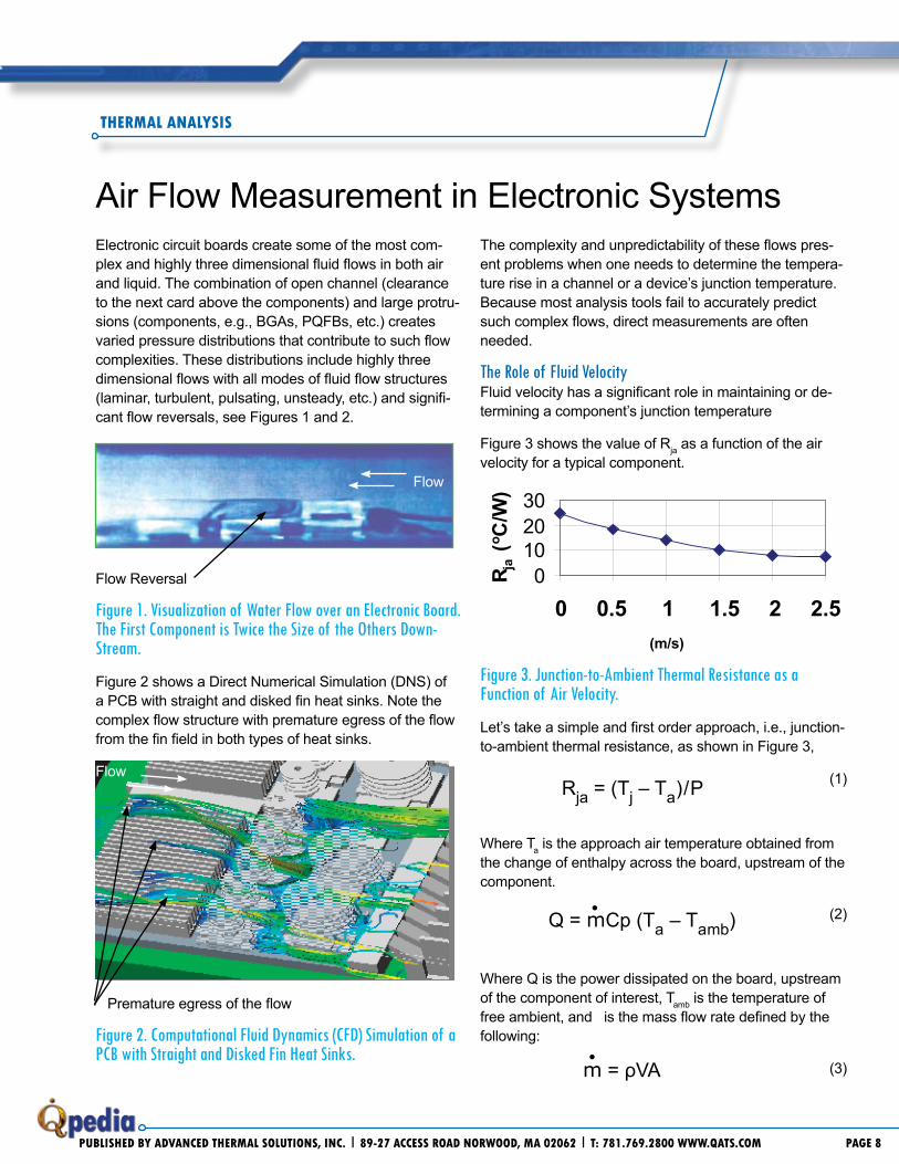
Electronic circuit boards create some of the most com-plex and highly three dimensional fluid flows in both air and liquid. The combination of open channel (clearance to the next card above the components) and large protru-sions (components, e.g., BGAs, PQFBs, etc.) creates varied pressure distributions that contribute to such flow complexities. These distributions include highly three dimensional flows with all modes of fluid flow structures (laminar, turbulent, pulsating, unsteady, etc.) and signifi-cant flow reversals, see Figures 1 and 2.
Flow
Flow Reversal
Figure 1. Visualization of Water Flow over an Electronic Board. The First Component is Twice the Size of the others Down-Stream.
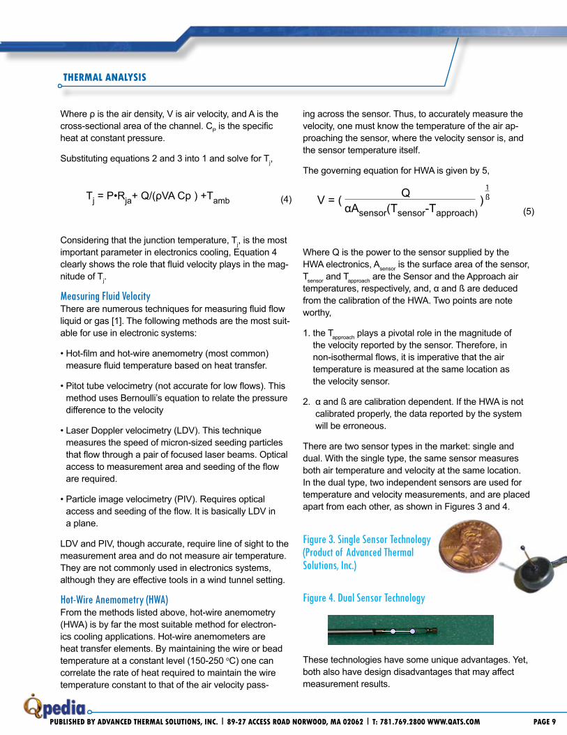
Figure 2 shows a Direct Numerical Simulation (DNS) of a PCB with straight and disked fin heat sinks. Note the complex flow structure with premature egress of the flow from the fin field in both types of heat sinks.
Flow
Premature egress of the flow
Figure 2. Computational Fluid Dynamics (CFD) Simulation of a pCB with Straight and Disked Fin Heat Sinks.
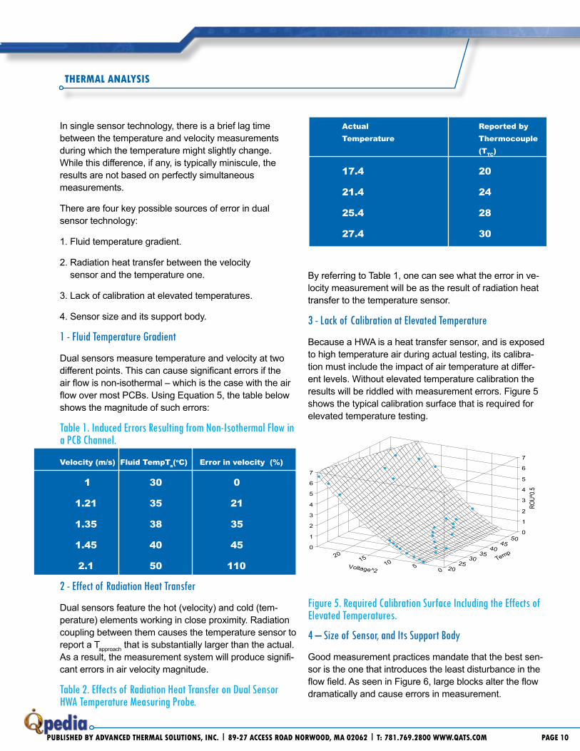
The complexity and unpredictability of these flows pres-ent problems when one needs to determine the tempera-ture rise in a channel or a device’s junction temperature. Because most analysis tools fail to accurately predict such complex flows, direct measurements are often needed.
The Role of Fluid Velocity Fluid velocity has a significant role in maintaining or de-termining a component’s junction temperature
Figure 3 shows the value of Rja as a function of the air velocity for a typical component.
00.511.522.5(m/s)
Figure 3. Junction-to-Ambient Thermal Resistance as a Function of Air Velocity.
Let’s take a simple and first order approach, i.e., junction-to-ambient thermal resistance, as shown in Figure 3,
(1)
Where Ta is the approach air temperature obtained from the change of enthalpy across the board, upstream of the component.
(2)
Where Q is the power dissipated on the board, upstream of the component of interest, Tamb is the temperature of free ambient, and is the mass flow rate defined by the following:
(3)
PublIshed by AdVAnced ThermAl soluTIons, Inc. | 89-27 Access roAd norwood, mA 02062 | T: 781.769.2800 www.qATs.com PAGe 9
ThermAl AnAlysIs
Where ρ is the air density, V is air velocity, and A is the cross-sectional area of the channel. CP is the specific heat at constant pressure.
Substituting equations 2 and 3 into 1 and solve for Tj,
(4)
Considering that the junction temperature, Tj, is the most important parameter in electronics cooling, Equation 4 clearly shows the role that fluid velocity plays in the mag-nitude of Tj.
Measuring Fluid Velocity There are numerous techniques for measuring fluid flow liquid or gas [1]. The following methods are the most suit-able for use in electronic systems:
• Hot-film and hot-wire anemometry (most common) measure fluid temperature based on heat transfer.
• Pitot tube velocimetry (not accurate for low flows). This method uses Bernoulli’s equation to relate the pressure difference to the velocity
• Laser Doppler velocimetry (LDV). This technique measures the speed of micron-sized seeding particles that flow through a pair of focused laser beams. Optical access to measurement area and seeding of the flow are required.
• Particle image velocimetry (PIV). Requires optical access and seeding of the flow. It is basically LDV in a plane.
LDV and PIV, though accurate, require line of sight to the measurement area and do not measure air temperature. They are not commonly used in electronics systems, although they are effective tools in a wind tunnel setting.
Hot-Wire Anemometry (HWA) From the methods listed above, hot-wire anemometry (HWA) is by far the most suitable method for electron-ics cooling applications. Hot-wire anemometers are heat transfer elements. By maintaining the wire or bead temperature at a constant level (150-250 oC) one can correlate the rate of heat required to maintain the wire temperature constant to that of the air velocity pass-
ing across the sensor. Thus, to accurately measure the velocity, one must know the temperature of the air ap-proaching the sensor, where the velocity sensor is, and the sensor temperature itself.
The governing equation for HWA is given by 5,
(5)
Where Q is the power to the sensor supplied by the HWA electronics, Asensor is the surface area of the sensor, Tsensor and Tapproach are the Sensor and the Approach air temperatures, respectively, and, α and ß are deduced from the calibration of the HWA. Two points are note worthy,
1. the Tapproach plays a pivotal role in the magnitude of the velocity reported by the sensor. Therefore, in non-isothermal flows, it is imperative that the air temperature is measured at the same location as the velocity sensor.
2. α and ß are calibration dependent. If the HWA is not calibrated properly, the data reported by the system will be erroneous.
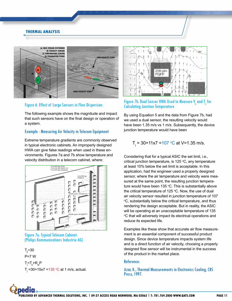
There are two sensor types in the market: single and dual. With the single type, the same sensor measures both air temperature and velocity at the same location. In the dual type, two independent sensors are used for temperature and velocity measurements, and are placed apart from each other, as shown in Figures 3 and 4.
Figure 3. Single Sensor Technology (product of Advanced Thermal Solutions, Inc.)
Figure 4. Dual Sensor Technology
These technologies have some unique advantages. Yet, both also have design disadvantages that may affect measurement results.
Rja = (Tj – Ta)/P
Q = mCp (Ta – Tamb)
m = ρVA
Tj = P•Rja+ Q/(ρVA Cp ) +Tamb
V = ( )
•
•
αAsensor(Tsensor-Tapproach)
Q 1ß
Rja = (Tj – Ta)/P
Q = mCp (Ta – Tamb)
m = ρVA
Tj = P•Rja+ Q/(ρVA Cp ) +Tamb
V = ( )
•
•
αAsensor(Tsensor-Tapproach)
Q 1ß
PublIshed by AdVAnced ThermAl soluTIons, Inc. | 89-27 Access roAd norwood, mA 02062 | T: 781.769.2800 www.qATs.com PAGe 10
ThermAl AnAlysIs
2025
3035
4045
50
Temp
05101520
Voltage^2
0
01
12
23
34
45
56
67
7
ROU^
0.5 ROU^
0.5
VelocitySensor
Stagnationpoint
Free streamdisturbed
TemperatureSensor
VelocitySensor
Stagnationpoint
Free streamdisturbed
TemperatureSensor
HighVelocity
flow
Low Velocity
Flow(separation)
HighVelocity
flow
Low Velocity
Flow(separation)
In single sensor technology, there is a brief lag time between the temperature and velocity measurements during which the temperature might slightly change. While this difference, if any, is typically miniscule, the results are not based on perfectly simultaneous measurements.
There are four key possible sources of error in dual sensor technology:
1. Fluid temperature gradient.
2. Radiation heat transfer between the velocity sensor and the temperature one.
3. Lack of calibration at elevated temperatures.
4. Sensor size and its support body.
1 - Fluid Temperature Gradient
Dual sensors measure temperature and velocity at two different points. This can cause significant errors if the air flow is non-isothermal – which is the case with the air flow over most PCBs. Using Equation 5, the table below shows the magnitude of such errors:
Table 1. Induced Errors Resulting from Non-Isothermal Flow in a pCB Channel.
Velocity (m/s) Fluid TempTa(oC) Error in velocity (%)
1 30 0
1.21 35 21
1.35 38 35
1.45 40 45
2.1 50 110
2 - Effect of Radiation Heat Transfer
Dual sensors feature the hot (velocity) and cold (tem-perature) elements working in close proximity. Radiation coupling between them causes the temperature sensor to report a Tapproach that is substantially larger than the actual. As a result, the measurement system will produce signifi-cant errors in air velocity magnitude.
Table 2. Effects of Radiation Heat Transfer on Dual Sensor HWA Temperature Measuring probe.
Actual Reported by Temperature Thermocouple (TTC)
17.4 20
21.4 24
25.4 28
27.4 30
By referring to Table 1, one can see what the error in ve-locity measurement will be as the result of radiation heat transfer to the temperature sensor.
3 - Lack of Calibration at Elevated Temperature
Because a HWA is a heat transfer sensor, and is exposed to high temperature air during actual testing, its calibra-tion must include the impact of air temperature at differ-ent levels. Without elevated temperature calibration the results will be riddled with measurement errors. Figure 5 shows the typical calibration surface that is required for elevated temperature testing.
Figure 5. Required Calibration Surface Including the Effects of Elevated Temperatures.
4 – Size of Sensor, and Its Support Body
Good measurement practices mandate that the best sen-sor is the one that introduces the least disturbance in the flow field. As seen in Figure 6, large blocks alter the flow dramatically and cause errors in measurement.
PublIshed by AdVAnced ThermAl soluTIons, Inc. | 89-27 Access roAd norwood, mA 02062 | T: 781.769.2800 www.qATs.com PAGe 11
ThermAl AnAlysIs
Figure 6. Effect of Large Sensors in Flow Dispersion.
The following example shows the magnitude and impact that such sensors have on the final design or operation of a system.
Example - Measuring Air Velocity in Telecom Equipment
Extreme temperature gradients are commonly observed in typical electronic cabinets. An improperly designed HWA can give false readings when used in these en-vironments. Figures 7a and 7b show temperature and velocity distribution in a telecom cabinet, where:
Figure 7a. Typical Telecom Cabinet. (philips Kommunications Industrie AG)
Ta=30
P=7 W
Tj=Ta+RjaP
Tj =30+15x7 =135 oC at 1 m/s, actual.
Figure 7b. Dual Sensor HWA Used to Measure Va and Ta for Calculating Junction Temperature
By using Equation 5 and the data from Figure 7b, had we used a dual sensor, the resulting velocity would have been 1.35 m/s vs 1 m/s. Subsequently, the device junction temperature would have been
Tj = 30+11x7 =107 oC at V=1.35 m/s.
Considering that for a typical ASIC the set limit, i.e., critical junction temperature, is 125 oC, any temperature at least 10% below the set limit is acceptable. In this application, had the engineer used a properly designed sensor, where the air temperature and velocity were mea-sured at the same point, the resulting junction tempera-ture would have been 135 oC. This is substantially above the critical temperature of 125 oC. Now, the use of dual air velocity sensor resulted in junction temperature of 107 oC, substantially below the critical temperature, and thus rendering the design acceptable. But in reality, the ASIC will be operating at an unacceptable temperature of 135 oC that will adversely impact its electrical operations and reduce its expected life.
Examples like these show that accurate air flow measure-ment is an essential component of successful product design. Since device temperature impacts system life and is a direct function of air velocity, choosing a properly designed flow sensor will be instrumental in the success of the product in the market place.
Reference:
Azar, K., Thermal Measurements in Electronics Cooling, CRS press, 1997.
(A) free sTreAm dIsTurbed (b) VelocITy sensor
(c) TemPerATure sensor (d) sTAGnATIon PoInT
(A)
(b)
(c)
(d)
hIGh VelocITy flow
low VelocITy flow

PublIshed by AdVAnced ThermAl soluTIons, Inc. | 89-27 Access roAd norwood, mA 02062 | T: 781.769.2800 www.qATs.com PAGe 12
My name is Mitch.
I am an applications engineer for a
networking equipment provider.
I still call my mother every Sunday.
I AM HoT (AND I’M NoT AFRAID To ADMIT IT)
They say the first step to solving your problems is admitting you have one. The second is calling us. Now that ADVANCED THERMAL SOLUTIONS, INC. has teamed up with DIGI-KEY, your electronics cooling solutions are only a click away.
Through Digi-Key, the global electronics components distributor, ATS now offers over 380 heat sinks for cooling BGAs and other hot-running semiconductor devices. The heat sinks are available for immediate delivery when purchased through Digi-Key’s Web site and printed catalogs.
Now you can easily get individual ATS heat sinks for prototypes and testing, or larger volumes for production requirements. And with Digi-Key’s online tools, you can check real-time inventory and order parts 24 hours a day, every day of the year.
C
NEW!
W
H
L
Be Cool. Get your catalog today. For an ATS heat sink catalog call 781.769.2800 or download it at qats.com. To place an order, check availability or view orders, visit digikey.com. Or call 1-800-DIGI-KEY.

PublIshed by AdVAnced ThermAl soluTIons, Inc. | 89-27 Access roAd norwood, mA 02062 | T: 781.769.2800 www.qATs.com PAGe 1�
ThermAl fundAmenTAls
One of the basic concepts of electronics cooling is effective transfer of heat from semiconductor devices to the ambient using heat sinks or other cooling technolo-gies. The effectiveness of this approach depends on a system’s total thermal resistance, which is composed of discrete thermal resistances on the path of heat from the source to the ambient. One of these resistances is spreading resistance.
Spreading resistance occurs whenever a small heat source comes in contact with the base of a larger heat sink. The heat does not distribute uniformly through the heat sink base, and consequently does not transfer ef-ficiently to the fins for convective cooling. Figure 1 shows a CFdesign® simulation solution for such an occurrence. The spreading resistance phenomenon is shown by how the heat travels through the center of a heat sink base causing a large temperature gradient between the center and edges of the heat sink.
Figure 1. CFdesign® Solution Showing Temperature Distribution at the Base of a Heat Sink.
Spreading resistance is an increasingly important issue in thermal management as microelectronic packages become more powerful and compact and larger heat sinks are required to cool these devices. In high heat flux applications, spreading resistance can comprise 60 to 70% of the total thermal resistance.
A good estimate of spreading resistance is required to manage heat effectively using conventional air-cooled heat sinks. There have been a number of theoretical and experimental studies to estimate spreading resistance. Two of the most notable methods belong to Yovanovich et al. [1] and to Gordon N. Ellison [2].
While these extensive studies cover all aspects of spreading resistance, they involve cumbersome infinite series and complicated coefficient terms. Fortunately, a simpler solution is provided by Lee et al. [3] that yield re-sults very close to those of complicated methods and can be easily programmed in any spreadsheet software. The solution is based on a circular spreader plate and circular heat source. Thus, square spreader plates and heating sources must be converted into circular geometries as shown in Figure 2.
Figure 2. Transformation of a Square Spreader and Heat Source Into Circular Geometry [4].
The transformation is based on the areas of the plate and the heat source being the same for both the square and circular geometries. So, the equivalent radii in the circular
Spreading Thermal Resistance; Its Definition and Control
0 10 20 30 4060
70
80
90
100
110
120
130
140
150
160
Surfa
cetem
pera
ure(
oC)
Distancefromcenter (mm)
z
z
00.2
0.40.6
0.81
1.2
1.41.6
1.82
0 0.5 1 1.5 2 2.5 3 3.5
Heat Sink Base Thickness (mm)
Spre
adin
gTh
erm
alR
esis
tanc
e(C
/W)
AluminumCopper
00.2
0.40.6
0.81
1.2
1.41.6
1.82
0 0.5 1 1.5 2 2.5 3 3.5
Heat Sink Base Thickness (mm)
Spre
adin
gTh
erm
alR
esis
tanc
e(C
/W)
AluminumCopper
00.2
0.40.6
0.81
1.2
1.41.6
1.82
0 0.5 1 1.5 2 2.5 3 3.5
Heat Sink Base Thickness (mm)
Spre
adin
gTh
erm
alR
esis
tanc
e(C
/W)
AluminumCopper

case are given by Equations 1 and 2:
(1) (2)
The equivalent radii, r1 and r2, may then be used along with the thermal conductivity, k, of the spreader plate with thickness, t, to obtain the spreading resistance from Equation 3 [4].
(3)
Equation 3 estimates the thermal conduction spreading resistance from the maximum temperature of a heat source to the convective surface on the top of the spreader plate. The parameters that are required to evaluate this equation are defined in Table 1. Table 1. Definitions of Terms Used in Spreading Resistance Equation 3.
ε =
λ =
t = Φ =
Bi = ψmax=
The accuracy of Equation 3 is tested in a study by R. E. Simons of IBM [4] which compares its results with those of the exact series solution developed by Ellison [2].
These calculations are based on a fixed heat input area of 10 x 10 mm on a square thermal spreader plate 2.5 mm thick and ranging in size from 20 x 20 mm to 40 x 40 mm. Two values of thermal conductivity were used, ranging from 25 W/m•K for a material such as Alumina, to 400 W/m•K for a material such as copper. Similarly, two values of heat transfer coefficient were used, ranging
from 250 W/m2•K to 1000 W/m2•K. These values repre-sent what could be achieved with low and high perfor-mance forced convection heat sinks, respectively [4].
A comparison of the results for the conduction/spread-ing thermal resistance, Rsp, reveals that the error for the simplified formula ranges between -2.1% to +4.8% over all parameters [4].
Spreading thermal resistance can be mitigated in a number of ways. One convenient and intuitive method is to simply increase the thickness of the base of a heat sink. However, one should realize that increasing the base thickness will always mean decreasing the height of the fins. A loss of the fins’ convective surfaces beyond a limit would offset the benefits of reduced spreading resistance. In estimating the spreading thermal resistance, the convective resistance must be evaluated at the same time to find the optimized thickness of the heat sink base.
Another way to lower the spreading thermal resistance is to use heat sinks made from materials with high thermal conductivity. The most commonly used material is Alumi-num due to its light weight, good conductivity, and ease of manufacturing. However, some applications require heat sinks with higher thermal conductivities. In these cases, Copper is often used because its thermal conductivity is twice that of aluminum. The main drawbacks of Copper are its high cost, weight, and difficulty to fabricate.
Figure 3 shows the effect of a heat sink’s base thickness and material on the spreading thermal resistance. To con-struct this figure, Equation 3 is used for a spreader plate 40 mm square, with a 10 mm square heat source. The convective heat transfer coefficient is assumed to be 27 W/m2•K. At first, as seen in the figure, thickening the base has a pronounced effect on the spreading resistance. However, this effect becomes less significant at subse-quently higher thicknesses. On the material side, Cop-per heat sinks consistently have a spreading resistance about half that of Aluminum heat sinks. This is because the thermal conductivity of Copper is about twice that of aluminum.
Rsp =k x r1 �
ψmax
�
S1 x S1r1 =
�
r2 = S2 x S2
r1
r2
t
r2
heff x r2
k
� +
tanh (λ x t) +
1 + tanh(λ x t)
ε x π 1 π π
1
ε �
λ
Biλ
Bi
+ (1- ε)Φ
Rsp =k x r1 �
ψmax
�
S1 x S1r1 =
�
r2 = S2 x S2
r1
r2
t
r2
heff x r2
k
� +
tanh (λ x t) +
1 + tanh(λ x t)
ε x π 1 π π
1
ε �
λ
Biλ
Bi
+ (1- ε)Φ
Rsp =k x r1 �
ψmax
�
S1 x S1r1 =
�
r2 = S2 x S2
r1
r2
t
r2
heff x r2
k
� +
tanh (λ x t) +
1 + tanh(λ x t)
ε x π 1 π π
1
ε �
λ
Biλ
Bi
+ (1- ε)Φ
Rsp =k x r1 �
ψmax
�
S1 x S1r1 =
�
r2 = S2 x S2
r1
r2
t
r2
heff x r2
k
� +
tanh (λ x t) +
1 + tanh(λ x t)
ε x π 1 π π
1
ε �
λ
Biλ
Bi
+ (1- ε)Φ
PublIshed by AdVAnced ThermAl soluTIons, Inc. | 89-27 Access roAd norwood, mA 02062 | T: 781.769.2800 www.qATs.com PAGe 1�
ThermAl fundAmenTAls
ThermAl fundAmenTAls
Figure 3. The Effect of a Heat Sink’s Material and Base Thickness on Thermal Spreading Resistance
In some high-heat flux applications where the heat sink needs to be considerably larger than a semiconductor die, thickening the base and/or use of copper heat sinks may not be adequate to compensate for the conduction losses in the base. In these instances, forced spreading devices need to be implemented. One device that can be very useful in reducing the component temperature is a heat pipe.
A heat pipe is a vacuum hollow tube that has a wick structure on its internal walls and has a small amount of coolant fluid [5]. The fluid becomes vaporized by absorb-ing the heat in the evaporative section of the heat pipe. Vaporized fluid will condense at the condenser section of the heat pipe. The condensed fluid is then drawn back to the evaporator side by capillary force of the wick structure and the cycle would continue. As a result, heat pipes if properly designed and manufactured, could have thermal conductivities of 10-50 times of a solid copper. Figure 4 depicts the internal structure of a heat pipe.
Figure 4. Internal Structure of a Heat pipe. [6]
Heat pipes can be embedded in the base of a heat sink to enhance the heat spreading at the base of the heat sink. The heat pipe spreads heat effectively across the sink base before it gets distributed to the fins. The result is more effective convective cooling since the fins’ base temperature will be higher, providing more effective use of the fins at the outer edge of the heat sink. There are several methods for embedding a heat pipe in a heat sink base. They can be completely embedded in the base or surface-embedded inside grooves machined into the base of a heat sink. In either case, conductive thermal epoxy is used to reduce the interfacial contact resistance between the heat pipe and the heat sink.
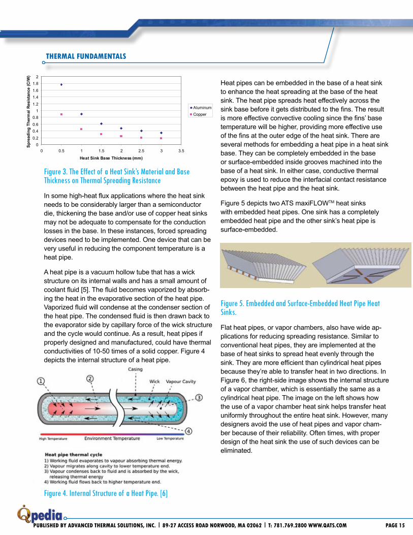
Figure 5 depicts two ATS maxiFLOWTM heat sinks with embedded heat pipes. One sink has a completely embedded heat pipe and the other sink’s heat pipe is surface-embedded.
Figure 5. Embedded and Surface-Embedded Heat pipe Heat Sinks.
Flat heat pipes, or vapor chambers, also have wide ap-plications for reducing spreading resistance. Similar to conventional heat pipes, they are implemented at the base of heat sinks to spread heat evenly through the sink. They are more efficient than cylindrical heat pipes because they’re able to transfer heat in two directions. In Figure 6, the right-side image shows the internal structure of a vapor chamber, which is essentially the same as a cylindrical heat pipe. The image on the left shows how the use of a vapor chamber heat sink helps transfer heat uniformly throughout the entire heat sink. However, many designers avoid the use of heat pipes and vapor cham-ber because of their reliability. Often times, with proper design of the heat sink the use of such devices can be eliminated.
0 10 20 30 4060
70
80
90
100
110
120
130
140
150
160
Surfa
cetem
pera
ure(
oC)
Distancefromcenter (mm)
z
z
00.2
0.40.6
0.81
1.2
1.41.6
1.82
0 0.5 1 1.5 2 2.5 3 3.5
Heat Sink Base Thickness (mm)
Spre
adin
gTh
erm
alR
esis
tanc
e(C
/W)
AluminumCopper
00.2
0.40.6
0.81
1.2
1.41.6
1.82
0 0.5 1 1.5 2 2.5 3 3.5
Heat Sink Base Thickness (mm)
Spre
adin
gTh
erm
alR
esis
tanc
e(C
/W)
AluminumCopper
00.2
0.40.6
0.81
1.2
1.41.6
1.82
0 0.5 1 1.5 2 2.5 3 3.5
Heat Sink Base Thickness (mm)
Spre
adin
gTh
erm
alR
esis
tanc
e(C
/W)
AluminumCopper
PublIshed by AdVAnced ThermAl soluTIons, Inc. | 89-27 Access roAd norwood, mA 02062 | T: 781.769.2800 www.qATs.com PAGe 15
ThermAl fundAmenTAls
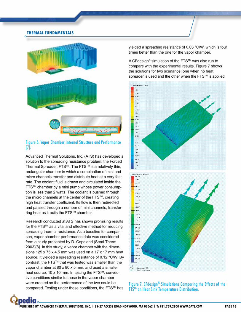
Figure 6. Vapor Chamber Internal Structure and performance [7].
Advanced Thermal Solutions, Inc. (ATS) has developed a solution to the spreading resistance problem: the Forced Thermal Spreader, FTSTM. The FTSTM is a relatively thin, rectangular chamber in which a combination of mini and micro channels transfer and distribute heat at a very fast rate. The coolant fluid is drawn and circulated inside the FTSTM chamber by a mini pump whose power consump-tion is less than 2 watts. The coolant is pushed through the micro channels at the center of the FTSTM, creating high heat transfer coefficient. Its flow is then redirected and passed through a number of mini channels, transfer-ring heat as it exits the FTSTM chamber.
Research conducted at ATS has shown promising results for the FTSTM as a vital and effective method for reducing spreading thermal resistance. As a baseline for compari-son, vapor chamber performance data was considered from a study presented by D. Copeland (Semi-Therm 2003)[8]. In this study, a vapor chamber with the dimen-sions 125 x 75 x 4.5 mm was used on a 17 x 17 mm heat source. It yielded a spreading resistance of 0.12 °C/W. By contrast, the FTSTM that was tested was smaller than the vapor chamber at 80 x 80 x 5 mm, and used a smaller heat source, 10 x 10 mm. In testing the FTSTM, convec-tive conditions similar to those in the vapor chamber were created so the performance of the two could be compared. Testing under these conditions, the FTSTM has
yielded a spreading resistance of 0.03 °C/W, which is four times better than the one for the vapor chamber.
A CFdesign® simulation of the FTSTM was also run to compare with the experimental results. Figure 7 shows the solutions for two scenarios: one when no heat spreader is used and the other when the FTSTM is applied.
Figure 7. CFdesign® Simulations Comparing the Effects of the FTSTM on Heat Sink Temperature Distribution.
PublIshed by AdVAnced ThermAl soluTIons, Inc. | 89-27 Access roAd norwood, mA 02062 | T: 781.769.2800 www.qATs.com PAGe 16

Figure 7 clearly shows that with FTSTM, the temperature throughout the heat sink on the left is uniform and substantially on the lower (cool) side of the temperature scale. As the bottom image shows, when the heat sink is used alone, the result is a high temperature concentration at the component area and much cooler temperatures elsewhere in the heat sink. This huge spreading resis-tance would keep the heat from being dissipated through the base and consequently the fins.
As semiconductor chips are made with more compact packaging and higher power densities, spreading re-sistance is becoming the dominant part of their cooling system’s total thermal resistance. In order to stay within the limits of air-cooled capabilities, spreading resistance must be properly managed based on available tech-niques and technology. Before investing in exotic and expensive solutions, it is worthwhile to determine whether the problem can be solved by simply optimizing the heat sink design parameters or considering a heat sink with higher thermal conductivity. References:
1. Yovanovich, M., Muzychka, Y. and Culham, J., Spreading Resistnace of Isoflux Rectangules and Strips on Com-pound Flux Channels, University of Waterloo, 1998
2. Ellison, G., Maximum Thermal Spreading Resistance for Rectangular Sources and plates With Nonunity Aspect Ratios, IEEE Trans. Comp., Hybrids, Manufac. Technol., Vol. 26, No. 2, 2003.
3. Lee, S., Song, S., Au, V., and Moran, K., Constriction/Spreading Resistance Model for Electronic packaging, proceedings of ASME/JSME Engineering Conference, Vol. 4, 1995.
4. Simons, R., Simple Formulas for Estimating Therma Spreading Resistance, Electronics Cooling, May 2004.
5. Advanced Thermal Solutions, Inc., Heat pipes: Heat Super Conductors, Qpedia, July 2007.
6. A. McCloskey, How Does a Heat pipe Work? Heat pipes Explained, http://www.ocmodshop.com/ocmodshop.aspx?a=920, August 15, 2007
7. Mehl Dale, Vapor Chamber Heat sinks Eliminate Hot Spots, Thermacore International, Inc.
8. Wei, J., Cha, A., Copeland, D., Measurement of Vapor Chamber performance, Semi-Therm Symposium, 2003.
PublIshed by AdVAnced ThermAl soluTIons, Inc. | 89-27 Access roAd norwood, mA 02062 | T: 781.769.2800 www.qATs.com PAGe 17
ThermAl fundAmenTAls
My name is Francisco.
I design GpS devices for the defense industry.
Yesterday, it took me a half-hour to find my car at the mall.
I AM HoT (AND I’M NoT AFRAID To ADMIT IT)
They say the first step to solving your problems is admitting you have one. The second is calling us. Now that ADVANCED THERMAL SOLUTIONS, INC. has teamed up with DIGI-KEY, your electronics cooling solutions are only a click away.
Visit www.Digikey.com to place an order or www.qats.com for further technical information.

PublIshed by AdVAnced ThermAl soluTIons, Inc. | 89-27 Access roAd norwood, mA 02062 | T: 781.769.2800 www.qATs.com PAGe 18
coolInG news
New Catalog Features 380+ Heat Sinks Available in 24 HoursNorwood, MA, August 7, 2007 – Over 380 heat sinks, available for overnight delivery exclusively from Digi-Key, are included in Advanced Thermal Solutions, Inc’s (ATS) new Heat Sink Catalog. Each of the heat sinks within the catalog is listed with part numbers, dimensions, thermal performance data and pricing.
The catalog includes a wide range of ATS maxiFLOW™ heat sinks which feature a low profile, spread fin array to maximize surface area for more effective convection (air) cooling. Testing at an air flow rate of just 0.5 m/s (100 ft/m) shows that device junction temperatures (Tj) can be reduced by more than 20 percent below the temperatures achieved using other heat sinks of comparable size and volume.
Also included in the catalog are heat sinks specifically designed for cooling a variety of Freescale processors and a wide range of BGAs, LGAs, ASICs and LED lighting strips. Straight-fin and cross-cut heat sinks can also be found in the catalog.
Most of the heat sinks in the new catalog are provided with thermally conductive adhesive mounting tapes or mechanical attachment systems for installation on hot components. These include the ATS maxiGRIP™ system, which features a stainless steel spring clip and plastic frame clip to provide secure attachment to the component and eliminates need to drill holes in the PCB. The system also allows for the use of high-performance phase-change materials that improve heat transfer as well as simple heat sink detachment and reattachment without damaging the component.
To receive a copy of the new Heat Sink Catalog by mail, please visit the ATS website www.qats.com and click on the “Ask the Experts” link or call 781-769-2800. An electronic version of the catalog is also available for download on the site.
The entire line of heat sinks can be found in the Digi-Key catalog on pages 1008 through 1011 or by visiting www.digikey.com. Orders can be placed online or by calling 1-800-DIGI-KEY.
1�Th InTernATIonAl WORKSHOp on ThermAl InVesTIGATIons of Ics And sysTems (ThermInIc ‘07) September 17-19, 2007 Budapest, Hungary
embedded sysTems conference bosTon September 18-21, 2007 Boston, MA USA
2007 ATs ThermAl mAnAGemenT TuTorIAl serIes october 4th, 2007 Norwood, MA USA High Capacity Cooling for Thermal Management
surfAce mounT TechnoloGy AssocIATIon (smTA InTernATIonAl 2007) october 7-11, 2007 Orlando, FL, USA
AdVAncedTcA summIT – wesT october 16-18, 2007 Santa Clara, CA USA
Zero downTIme 2007 November 5-7, 2007 Scottsdale, AZ, USA Electronics Cooling: Challenges & Solutions
�0Th InTernATIonAl symPosIum on mIcroelecTronIcs (ImAPs 2007) November 11-15, 2007 San Jose, CA, USA
2007 ATs ThermAl mAnAGemenT TuTorIAl serIes November 15th, 2007 Norwood, MA USA Thermal Management Methods in Electronics Cooling
EVENTS
C
NEW!
W
H
L

PublIshed by AdVAnced ThermAl soluTIons, Inc. | 89-27 Access roAd norwood, mA 02062 | T: 781.769.2800 www.qATs.com PAGe 19
who we Are
Advanced Thermal Solutions is a leading engineering and manufacturing company supplying complete thermal and mechanical packaging solutions from analysis and testing to final production. ATS provides a wide range of air and liquid cooling solutions, laboratory-quality thermal instrumentation, along with thermal design consulting services and training. Each article within Qpedia is meticulously researched and written by ATS’ engineering staff. For more informa-tion about Advanced Thermal Solutions, Inc., please visit www.qats.com or call 781-769-2800.
AdVAnced ThermAl soluTIons, Inc. United States89-27 Access Road, Norwood, MA 02062T: 781.769.2800 | F: 781.769.9979 | www.qats.com
EuropeDe Nieuwe Vaart 50 | 1401 GS Bussum | The NetherlandsT: +31 (0) 3569 84715 | F: +31 (0) 3569 21294www.qats-europe.com