Embed Size (px)
Citation preview

Fundamentals of Power Electronics 1 Chapter 19: Resonant Conversion
• I plan on indicating for each lecture(s) of this year the equivalent lecture(s) from Spr. 06. This will make it easy if you choose to watch those lectures to stay in synch with this years class if we should run at a slightly different pace. I will also indicate if there is any new material for this year not covered in Spr. 06 so you will know to watch / attend that particular lecture this year. Similarly, any material covered in Spr. 06 but not covered this year will not show up as an equivalent lecture so you will know you can skip it.
• Today (lecture 4) we will cover material covered in lecture 7 of the Spr. 06 class. You may wish to watch some of Spring 06 lectures 1 to 3 for some valuable insight and historical perspective on resonant power conversion techniques.
ECEN 5817Housekeeping

Fundamentals of Power Electronics 2 Chapter 19: Resonant Conversion
2 different ways to construct transfer function H

Fundamentals of Power Electronics 3 Chapter 19: Resonant Conversion
Dc conversion ratio of the PRC
At resonance, this becomes
• PRC can step up the voltage, provided R > R0
• PRC can produce M approaching infinity, provided output current is limited to value less than Vg / R0

Fundamentals of Power Electronics 4 Chapter 19: Resonant Conversion
Model: series resonant converter

Fundamentals of Power Electronics 5 Chapter 19: Resonant Conversion
Comparison of approximate and exact characteristics
0.5 0.6 0.7 0.8 0.9 1.0
0.0
0.2
0.4
0.6
0.8
1.0
exact M, Q=2approx M, Q=2exact M, Q=10approx M, Q=10exact M, Q=0.5approx M, Q=0.5
F
M =
V/V
g
1 2 3 4 5
0.0
0.2
0.4
0.6
0.8
1.0
exact M, Q=0.5approx M, Q=0.5exact M, Q=10approx M, Q=10exact M, Q=2approx M, Q=2
F
M=
V/V
g
Series resonant converter
Below resonance:
0.5 < F < 1
Above resonance:
1 < F

Fundamentals of Power Electronics 6 Chapter 19: Resonant Conversion
Comparison of approximate and exact characteristics
Parallel resonant converterExact equation:
solid lines
Sinusoidal approximation: shaded lines

Fundamentals of Power Electronics 7 Chapter 19: Resonant Conversion
Chapter 19
Resonant Conversion
Introduction
19.1 Sinusoidal analysis of resonant converters
19.2 ExamplesSeries resonant converterParallel resonant converter
19.3 Soft switchingZero current switchingZero voltage switching
19.4 Load-dependent properties of resonant converters
19.5 Exact characteristics of the series and parallel resonant converters

Fundamentals of Power Electronics 8 Chapter 19: Resonant Conversion
19.3 Soft switching
Soft switching can mitigate some of the mechanisms of switching loss and possibly reduce the generation of EMI
Losses due to high voltage and high current present in switch during transitions, Losses due to shorting device capacitances
Semiconductor devices are switched on or off at the zero crossing of their voltage or current waveforms:
Zero-current switching: transistor turn-off transition occurs at zero current. Zero-current switching eliminates the switching loss caused by IGBT current tailing and by stray inductances. It can also be used to commutate SCR’s.
Zero-voltage switching: transistor turn-on transition occurs at zero voltage. Diodes may also operate with zero-voltage switching. Zero-voltage switching eliminates the switching loss induced by diode stored charge and device output capacitances.
Zero-voltage switching is usually preferred in modern converters, including soft-switching PWM converters.

Fundamentals of Power Electronics 9 Chapter 19: Resonant Conversion
19.3.1 Operation of the full bridge below resonance: Zero-current switching
Series resonant converter example
L
+–Vg
CQ1
Q2
Q3
Q4
D1
D2
D3
D4
+
vs(t)
– is(t)
+
vds1(t)
–iQ1(t)
Current bi-directional switches
ZCS vs. ZVS depends on tank current zero crossings with respect to transistor switching times = tank voltage zero crossings
Operation below resonance: input tank current leads voltage
Zero-current switching (ZCS) occurs

Fundamentals of Power Electronics 10 Chapter 19: Resonant Conversion
Tank input impedance
Re
|| Zi ||
f0
L
R0
Qe = R0 /Re
Operation below resonance: tank input impedance Zi is dominated by tank capacitor.
Zi is negative, and tank input current leads tank input voltage.
Zero crossing of the tank input current waveform is(t) occurs before the zero crossing of the voltage vs(t) – before switch transitions

Fundamentals of Power Electronics 11 Chapter 19: Resonant Conversion
Switch network waveforms, below resonanceZero-current switching
t
vs(t)
Vg
– Vg
vs1(t)
t
is(t)
t
Q1
Q4
D1
D4
Q2
Q3
D2
D3
Conductingdevices:
“Hard”turn-on of
Q1, Q4
“Soft”turn-off of
Q1, Q4
“Hard”turn-on of
Q2, Q3
“Soft”turn-off of
Q2, Q3
L
+–Vg
CQ1
Q2
Q3
Q4
D1
D2
D3
D4
+
vs(t)
– is(t)
+
vds1(t)
–iQ1(t)
Conduction sequence: Q1–D1–Q2–D2
Tank current is negative at the end of each half interval – antiparallel diodes conduct after their respective switches
Q1 is turned off during D1 conduction interval, without loss

Fundamentals of Power Electronics 12 Chapter 19: Resonant Conversion
Classical but misleading example: Transistor switchingwith clamped inductive load (4.3.1)
Buck converter example
transistor turn-off transition
Loss:

Fundamentals of Power Electronics 13 Chapter 19: Resonant Conversion
Switch network waveforms, below resonanceZero-current switching
t
vs(t)
Vg
– Vg
vs1(t)
t
is(t)
t
Q1
Q4
D1
D4
Q2
Q3
D2
D3
Conductingdevices:
“Hard”turn-on of
Q1, Q4
“Soft”turn-off of
Q1, Q4
“Hard”turn-on of
Q2, Q3
“Soft”turn-off of
Q2, Q3
L
+–Vg
CQ1
Q2
Q3
Q4
D1
D2
D3
D4
+
vs(t)
– is(t)
+
vds1(t)
–iQ1(t)
Conduction sequence: Q1–D1–Q2–D2
Q1 is turned off during D1 conduction interval, without loss
Note on terminology:

Fundamentals of Power Electronics 14 Chapter 19: Resonant Conversion
ZCS turn-on transition: hard switching
L
+–Vg
CQ1
Q2
Q3
Q4
D1
D2
D3
D4
+
vs(t)
– is(t)
+
vds1(t)
–iQ1(t)
Q1 turns on while D2 is conducting. Stored charge of D2 and of semiconductor output capacitances must be removed. Transistor turn-on transition is identical to hard-switched PWM, and switching loss occurs.
t
ids(t)
tQ1
Q4
D1
D4
Q2
Q3
D2
D3
Conductingdevices:
“Hard”turn-on of
Q1, Q4
“Soft”turn-off of
Q1, Q4
t
Vgvds1(t)

Fundamentals of Power Electronics 15 Chapter 19: Resonant Conversion

Fundamentals of Power Electronics 16 Chapter 19: Resonant Conversion
More on diode reverse recovery
Circuits with diode and switch in loop – when turn on switch diode turns off (unless ZVS)

Fundamentals of Power Electronics 17 Chapter 19: Resonant Conversion
More on diode reverse recovery
In steady-state:
Diode equations:
•
•
Stored minority charge profile underforward-biased conditions

Fundamentals of Power Electronics 18 Chapter 19: Resonant Conversion
Induced losses
•Stored charge is exponential function of voltage - require large change in q to get small change in vD
•vD remains > 0 until all stored charge removed – holding voltage across MOSFET = Vg while MOSFET is providing not only iL, but diode reverse current as well.
•Induces losses in MOSFET
•This energy loss is MUCH greater than the energy stored in diode in the form of stored charge as well as across depletion capacitance
rgrLgloss QVtIVW

Fundamentals of Power Electronics 19 Chapter 19: Resonant Conversion
19.3.2 Operation of the full bridge above resonance: Zero-voltage switching
Series resonant converter example
L
+–Vg
CQ1
Q2
Q3
Q4
D1
D2
D3
D4
+
vs(t)
– is(t)
+
vds1(t)
–iQ1(t)
Operation above resonance: input tank current lags voltage
Zero-voltage switching (ZVS) occurs
Fundamentals of Power Electronics 20 Chapter 19: Resonant Conversion
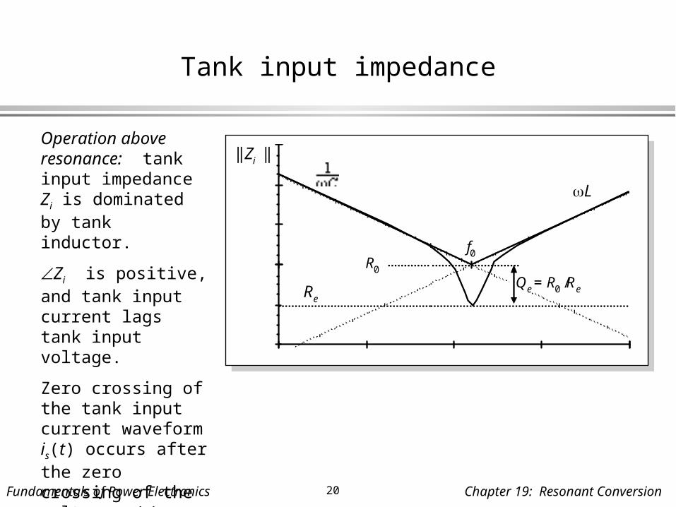
Tank input impedance
Re
|| Zi ||
f0
L
R0
Qe = R0 /Re
Operation above resonance: tank input impedance Zi is dominated by tank inductor.
Zi is positive, and tank input current lags tank input voltage.
Zero crossing of the tank input current waveform is(t) occurs after the zero crossing of the voltage vs(t) – after switch transitions

Fundamentals of Power Electronics 21 Chapter 19: Resonant Conversion
Switch network waveforms, above resonanceZero-voltage switching
L
+–Vg
CQ1
Q2
Q3
Q4
D1
D2
D3
D4
+
vs(t)
– is(t)
+
vds1(t)
–iQ1(t)
Conduction sequence: D1–Q1–D2–Q2
Tank current is negative at the beginning of each half-interval – antiparallel diodes conduct before their respective switches
Q1 is turned on during D1 conduction interval, without loss – D2 already off!
t
vs(t)
Vg
– Vg
vs1(t)
t
is(t)
t
Q1
Q4
D1
D4
Q2
Q3
D2
D3
Conductingdevices:
“Soft”turn-on of
Q1, Q4
“Hard”turn-off of
Q1, Q4
“Soft”turn-on of
Q2, Q3
“Hard”turn-off of
Q2, Q3

Fundamentals of Power Electronics 22 Chapter 19: Resonant Conversion
ZVS turn-off transition: hard switching?
L
+–Vg
CQ1
Q2
Q3
Q4
D1
D2
D3
D4
+
vs(t)
– is(t)
+
vds1(t)
–iQ1(t)
When Q1 turns off, D2 must begin conducting. Voltage across Q1 must increase to Vg. Transistor turn-off transition is identical to hard-switched PWM. Switching loss may occur… but….
t
ids(t)
Conductingdevices:
t
Vgvds1(t)
t
Q1
Q4
D1
D4
Q2
Q3
D2
D3
“Soft”turn-on of
Q1, Q4
“Hard”turn-off of
Q1, Q4

Fundamentals of Power Electronics 23 Chapter 19: Resonant Conversion
Classical but misleading example: Transistor switchingwith clamped inductive load (4.3.1)
Buck converter example
transistor turn-off transition
Loss:
Fundamentals of Power Electronics 24 Chapter 19: Resonant Conversion
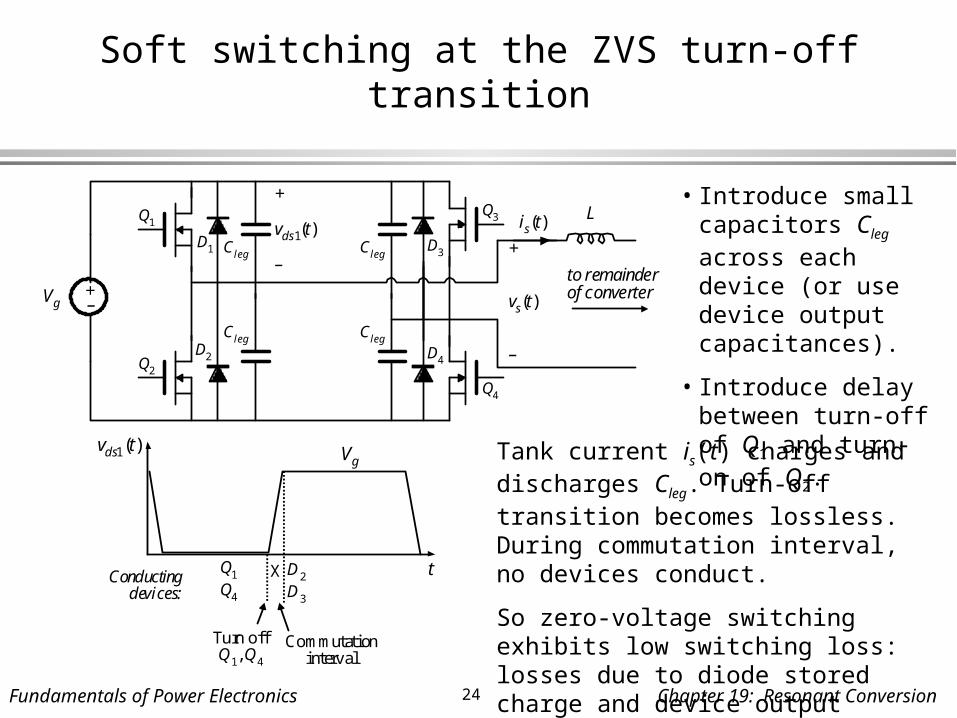
Soft switching at the ZVS turn-off transition
L
+–Vg
Q1
Q2
Q3
Q4
D1
D2
D3
D4
+
vs(t)
–
is(t)
+
vds1(t)
–to remainderof converter
Cleg
Cleg Cleg
Cleg
Conductingdevices:
t
Vgvds1(t)
Q1
Q4
D2
D3
Turn offQ1, Q4
Commutationinterval
X
• Introduce small capacitors Cleg across each device (or use device output capacitances).
• Introduce delay between turn-off of Q1 and turn-on of Q2.
Tank current is(t) charges and discharges Cleg. Turn-off transition becomes lossless. During commutation interval, no devices conduct.
So zero-voltage switching exhibits low switching loss: losses due to diode stored charge and device output capacitances are eliminated.
Fundamentals of Power Electronics 25 Chapter 19: Resonant Conversion
19.4 Load-dependent propertiesof resonant converters
Resonant inverter design objectives:
1. Operate with a specified load characteristic and range of operating points• With a nonlinear load, must properly match inverter output
characteristic to load characteristic
2. Obtain zero-voltage switching or zero-current switching• Preferably, obtain these properties at all loads• Could allow ZVS property to be lost at light load, if necessary
3. Minimize transistor currents and conduction losses• To obtain good efficiency at light load, the transistor current should
scale proportionally to load current (in resonant converters, it often doesn’t!)