Embed Size (px)
Citation preview

SCHOOL OF ELECTRICAL AND ELECTRONICS
DEPARTMENT OF ELECTRICAL AND ELECTRONICS
FUNDAMENTALS OF DIGITAL SYSTEMS-SCSA1201
UNIT – I - NUMBER SYSTEMS, COMPLEMENTS AND CODES

UNIT I-NUMBER SYSTEMS, COMPLEMENTS AND CODES
Number Systems - Binary Numbers - Number base conversions - Octal and Hexa Decimal Numbers - Complements - Signed
Binary Numbers - Binary Arithmetic - Binary Codes - Decimal Code - Error Detection code - Gray Code- Reflection and Self
Complementary codes - BCD number representation - Alphanumeric codes ASCII/EBCDIC - Hamming Code- Generation, Error
Correction.
1.1 Number System
A number system relates quantities and symbols. In digital system how information is represented is key
and there are different radices, i.e. number bases, which a numbering system can use.
Digital computer
Any class of devices capable of solving problems by processing information in discrete form. It operates on
data, including letters and symbols, which are expressed in binary form i.e using only two digits 0 and 1.
The block diagram of digital computer is given below:
The memory unit stores programs as well as input, output and intermediate data. The processor unit
performs arithmetic and other data processing tasks as specified by the program.The control unit
supervises the flow of information between various units. The program and data prepared by the user
are transferred into the memory unit by means of an input device such as punch card reader (or) tele
typewriter. An output device, such as printer, receives the result of the computations and the printed
results are presented to the user.
Number Representation:
Control Unit Processor (or)
Arithmetic unit
Storage (or)
Memory Unit
Output
Devices and
Control
Input
Devices and
Control

It can have different base values like: binary (base-2), octal (base-8), decimal (base 10) and
hexadecimal (base 16),here the base number represents the number of digits used in that numbering
system. As an example, in decimal numbering system the digits used are: 0, 1, 2, 3, 4, 5, 6, 7, 8 and 9.
Therefore the digits for binary are: 0 and 1, the digits for octal are: 0, 1, 2, 3, 4, 5, 6 and 7. For the
hexadecimal numbering system, base 16, the digits are: 0, 1, 2, 3, 4, 5, 6, 7, 8, 9, A, B, C, D, E, F.
2. Binary numbers
Numbers that contain only two digit 0 and 1 are called Binary Numbers. Each 0 or 1 is called a Bit,
from binary digit. A binary number of 4 bits is called a Nibble. A binary number of 8 bits is called a
Byte. A binary number of 16 bits is called a Word on some systems, on others a 32-bit number is called
a Word while a 16-bit number is called a Halfword.
Using 2 bit 0 and 1 to form
a binary number of 1 bit, numbers are 0 and 1
a binary number of 2 bit, numbers are 00, 01, 10, 11
a binary number of 3 bit, such numbers are 000, 001, 010, 011, 100, 101, 110, 111
a binary number of 4 bit, such numbers are 0000, 0001, 0010, 0011, 0100, 0101, 0110, 0111, 1000,
1001, 1010, 1011, 1100,1101,1110,1111
Therefore , using n bits there are 2n binary numbers of n bits
Each digit in a binary number has a value or weight. The LSB has a value of 1. The second from the right
has a value of 2, the next 4 , etc.,
16 8 4 2 1
24 2
3 2
2 2
1 2
0
The binary equivalent for some decimal numbers are given below.
Decimal 0 1 2 3 4 5 6 7 8 9 10 11
Binary 0 1 10 11 100 101 110 111 1000 1001 1010 1011
3. Number Base Conversions
3.1 Conversion of decimal number to any number system Step 1 convert the integer part by doing successive division using the radix of asked number systems. Step 2 convert the fractional part by doing successive multiplication using radix of asked number system 3.2 Conversion of decimal to binary number system The radix of asked number system is 2
Convert 8710 to ( )2
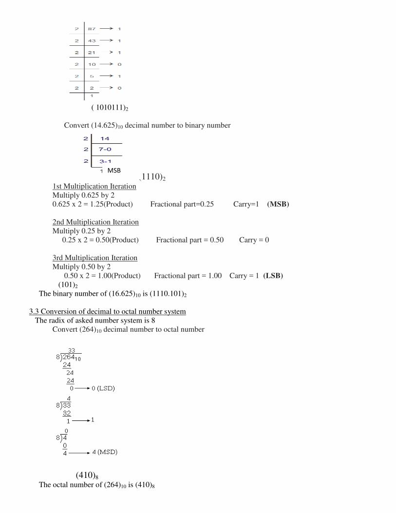
( 1010111)2
Convert (14.625)10 decimal number to binary number
(1110)2
1st Multiplication Iteration Multiply 0.625 by 2 0.625 x 2 = 1.25(Product) Fractional part=0.25 Carry=1 (MSB) 2nd Multiplication Iteration Multiply 0.25 by 2 0.25 x 2 = 0.50(Product) Fractional part = 0.50 Carry = 0 3rd Multiplication Iteration Multiply 0.50 by 2 0.50 x 2 = 1.00(Product) Fractional part = 1.00 Carry = 1 (LSB) (101)2
The binary number of (16.625)10 is (1110.101)2
3.3 Conversion of decimal to octal number system The radix of asked number system is 8
Convert (264)10 decimal number to octal number
(410)8
The octal number of (264)10 is (410)8
MSB
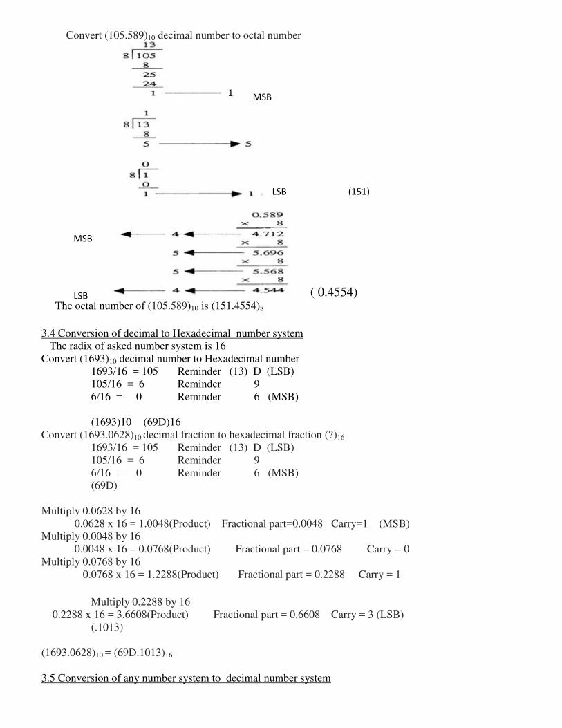
Convert (105.589)10 decimal number to octal number
( 0.4554) The octal number of (105.589)10 is (151.4554)8
3.4 Conversion of decimal to Hexadecimal number system The radix of asked number system is 16 Convert (1693)10 decimal number to Hexadecimal number
1693/16 = 105 Reminder (13) D (LSB) 105/16 = 6 Reminder 9 6/16 = 0 Reminder 6 (MSB) (1693)10 (69D)16
Convert (1693.0628)10 decimal fraction to hexadecimal fraction (?)16 1693/16 = 105 Reminder (13) D (LSB) 105/16 = 6 Reminder 9 6/16 = 0 Reminder 6 (MSB) (69D)
Multiply 0.0628 by 16 0.0628 x 16 = 1.0048(Product) Fractional part=0.0048 Carry=1 (MSB)
Multiply 0.0048 by 16 0.0048 x 16 = 0.0768(Product) Fractional part = 0.0768 Carry = 0 Multiply 0.0768 by 16
0.0768 x 16 = 1.2288(Product) Fractional part = 0.2288 Carry = 1
Multiply 0.2288 by 16
0.2288 x 16 = 3.6608(Product) Fractional part = 0.6608 Carry = 3 (LSB) (.1013)
(1693.0628)10 = (69D.1013)16
3.5 Conversion of any number system to decimal number system
1
LSB (151)
MSB
MSB
LSB
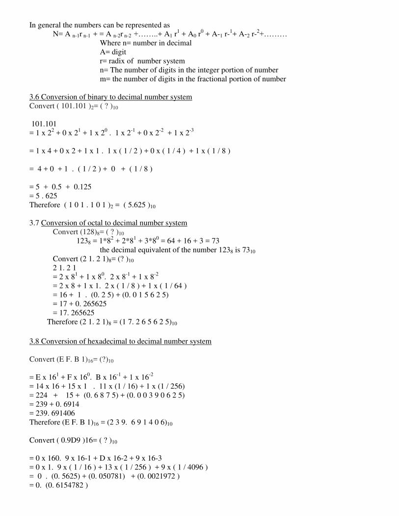
In general the numbers can be represented as N= A n-1r n-1 + = A n-2r n-2 +……..+ A1 r
1 + A0 r0 + A-1 r-
1+ A-2 r-2+………
Where n= number in decimal A= digit r= radix of number system n= The number of digits in the integer portion of number m= the number of digits in the fractional portion of number
3.6 Conversion of binary to decimal number system Convert ( 101.101 )2= ( ? )10 101.101 = 1 x 22 + 0 x 21 + 1 x 20 . 1 x 2-1 + 0 x 2-2 + 1 x 2-3
= 1 x 4 + 0 x 2 + 1 x 1 . 1 x ( 1 / 2 ) + 0 x ( 1 / 4 ) + 1 x ( 1 / 8 ) = 4 + 0 + 1 . ( 1 / 2 ) + 0 + ( 1 / 8 ) = 5 + 0.5 + 0.125 = 5 . 625 Therefore ( 1 0 1 . 1 0 1 )2 = ( 5.625 )10 3.7 Conversion of octal to decimal number system
Convert (128)8= ( ? )10 1238 = 1*82 + 2*81 + 3*80 = 64 + 16 + 3 = 73
the decimal equivalent of the number 1238 is 7310 Convert (2 1. 2 1)8= (? )10 2 1. 2 1
= 2 x 81 + 1 x 80. 2 x 8-1 + 1 x 8-2 = 2 x 8 + 1 x 1. 2 x ( 1 / 8 ) + 1 x ( 1 / 64 ) = 16 + 1 . (0. 2 5) + (0. 0 1 5 6 2 5) = 17 + 0. 265625 = 17. 265625
Therefore (2 1. 2 1)8 = (1 7. 2 6 5 6 2 5)10
3.8 Conversion of hexadecimal to decimal number system Convert (E F. B 1)16= (?)10
= E x 161 + F x 160. B x 16-1 + 1 x 16-2 = 14 x 16 + 15 x 1 . 11 x (1 / 16) + 1 x (1 / 256) = 224 + 15 + (0. 6 8 7 5) + (0. 0 0 3 9 0 6 2 5) = 239 + 0. 6914 = 239. 691406 Therefore (E F. B 1)16 = (2 3 9. 6 9 1 4 0 6)10 Convert ( 0.9D9 )16= ( ? )10 = 0 x 160. 9 x 16-1 + D x 16-2 + 9 x 16-3 = 0 x 1. 9 x ( 1 / 16 ) + 13 x ( 1 / 256 ) + 9 x ( 1 / 4096 ) = 0 . (0. 5625) + (0. 050781) + (0. 0021972 ) = 0. (0. 6154782 )

= 0. 6154782
3.9 Conversion of binary to octal number system
Convert (101101001)2 to ( )8 Divide the binary into group of three digits from LSB we will find the following pattern 101|101|001 Now writing the equivalent decimal number of each group we get 5 | 5 | 1 So the equivalent octal number is 5518
Convert 11001100.101 to ( )8
011|001|100. |101| 3 1 4 . 5 So the equivalent octal number is 314.5
3.10 Conversion of binary to hexadecimal number system Convert 111100010 to ( )16
Divide the binary into group of four digits from LSB 0001|1110|0010 Now writing the equivalent hexadecimal number of each group
1|E|2 So the equivalent Hexa decimal number is 1E216
Convert 11000011001.101 to ( )16 0110|0001|1001|.1010| 6 1 9 . A
So the equivalent Hexa decimal number is 619.A16
3.11 Conversion of octal number system to hexa decimal number system
Convert ( 25)8 to ( )16 First convert octal to binary The binary equivalent of 25 is 010101 Divide the binary into group of four digits from LSB
0001|0101 1 5 So the equivalent Hexa decimal number is 1516
3.12 Conversion of hexa decimal number system to octal number system Convert ( 1A.2B)16 to ( )8
First convert hexadecimal to binary The binary equivalent of 1A.2B is 00011010.00101011 Divide the binary into group of Three digits 011|010|.|001|010|110 3 2 . 1 2 6
so the equivalent octal number is 32.1268
4. COMPLEMENTS In digital computers to simplify the subtraction operation and for logical manipulation complements
are used . There are two types of complements for each radix system the radix complement and diminished radix complement. The first is referred to as the r’s complement and the second as the (r-1)’s complement.
r’s Complement Given a positive number N in base r with an integer part of n digits, the r’s complement of N is defined as rn-N if N≠0 and 0 if N=0
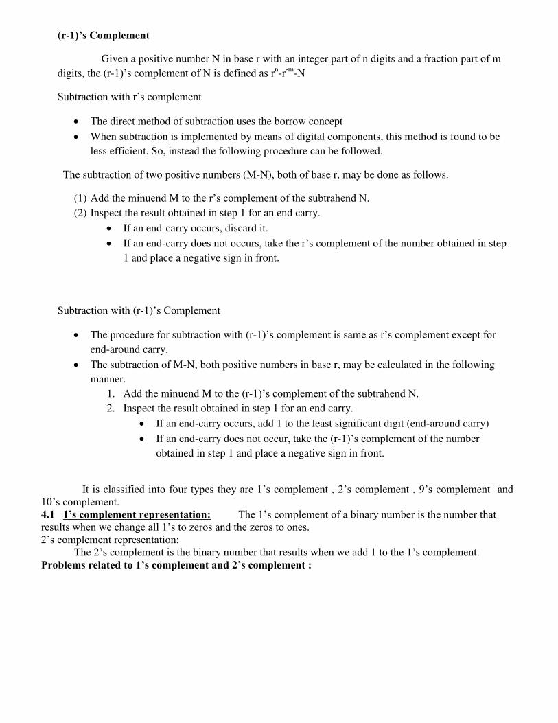
(r-1)’s Complement
Given a positive number N in base r with an integer part of n digits and a fraction part of m
digits, the (r-1)’s complement of N is defined as rn-r-m-N
Subtraction with r’s complement
The direct method of subtraction uses the borrow concept
When subtraction is implemented by means of digital components, this method is found to be
less efficient. So, instead the following procedure can be followed.
The subtraction of two positive numbers (M-N), both of base r, may be done as follows.
(1) Add the minuend M to the r’s complement of the subtrahend N. (2) Inspect the result obtained in step 1 for an end carry.
If an end-carry occurs, discard it.
If an end-carry does not occurs, take the r’s complement of the number obtained in step
1 and place a negative sign in front.
Subtraction with (r-1)’s Complement
The procedure for subtraction with (r-1)’s complement is same as r’s complement except for end-around carry.
The subtraction of M-N, both positive numbers in base r, may be calculated in the following
manner.
1. Add the minuend M to the (r-1)’s complement of the subtrahend N. 2. Inspect the result obtained in step 1 for an end carry.
If an end-carry occurs, add 1 to the least significant digit (end-around carry)
If an end-carry does not occur, take the (r-1)’s complement of the number obtained in step 1 and place a negative sign in front.
It is classified into four types they are 1’s complement , 2’s complement , 9’s complement and 10’s complement. 4.1 1’s complement representation: The 1’s complement of a binary number is the number that results when we change all 1’s to zeros and the zeros to ones. 2’s complement representation: The 2’s complement is the binary number that results when we add 1 to the 1’s complement. Problems related to 1’s complement and 2’s complement :
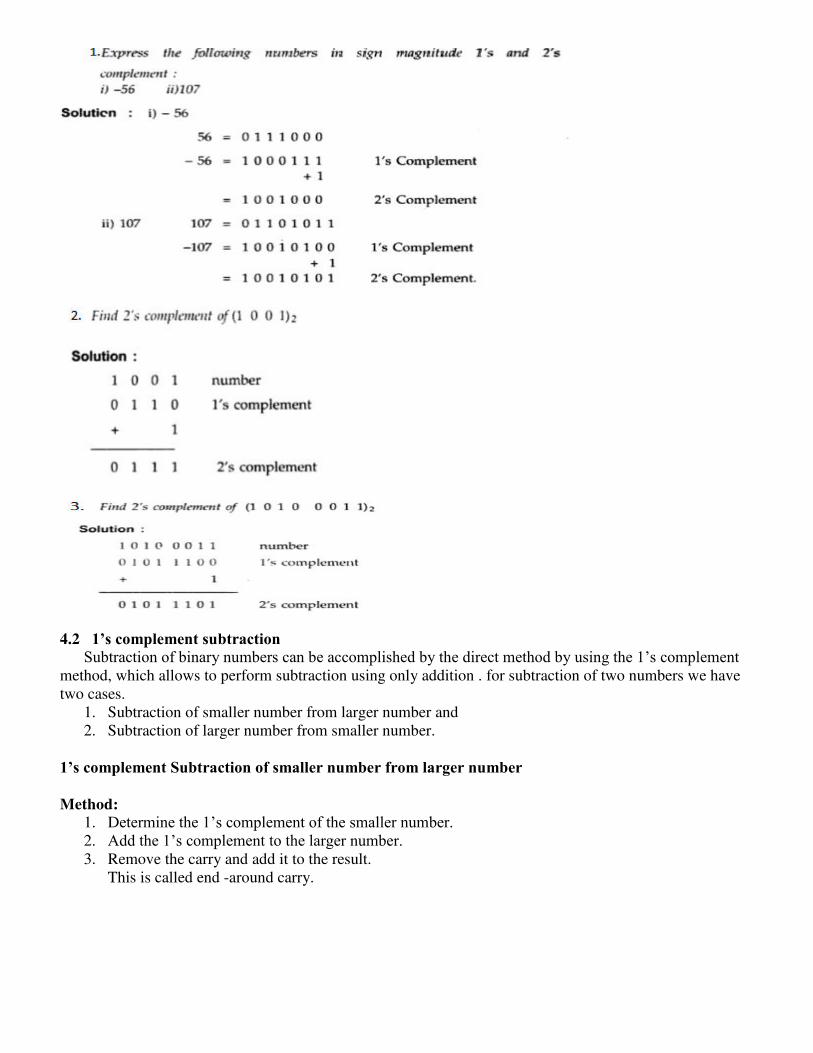
4.2 1’s complement subtraction
Subtraction of binary numbers can be accomplished by the direct method by using the 1’s complement method, which allows to perform subtraction using only addition . for subtraction of two numbers we have two cases.
1. Subtraction of smaller number from larger number and 2. Subtraction of larger number from smaller number.
1’s complement Subtraction of smaller number from larger number
Method:
1. Determine the 1’s complement of the smaller number. 2. Add the 1’s complement to the larger number. 3. Remove the carry and add it to the result.
This is called end -around carry.

1’s complement Subtraction of larger number from smaller number
Method:
1. Determine the 1’s complement of the larger number. 2. Add the 1’s complement to the smaller number. 3. Answer is in 1’s complement form. To get the answer in true form take the 1’s complement and
assign negative sign to the answer.
Advantages of 1’s complement subtraction :
1. The 1’s complement subtraction can be accomplished with an binary adder. Therefore , this method is useful in arithmetic logic circuits.
2. The 1’s complement of a number is easily obtained by inverting each bit in the number. 4.3 2’s complement Subtraction:
Like 1’s complement subtraction, in 2’s complement subtraction, the subtraction is accomplished by only addition.
2’s complement Subtraction of smaller number from larger number
Method
1. Determine the 2’s complement of the smaller number. 2. Add the 2’s complement to the larger number. 3. Discard the carry.
2’s complement Subtraction of larger number from smaller number
Method:
1. Determine the 2’s complement of the larger number. 2. Add the 2’s complement to the smaller number.

3. Answer is in 2’s complement form. To get the answer in true form take the 2’s complement and assign negative sign to the answer.
4.4 9's complement and 10's complement
Before knowing about 9's complement and 10's complement we should know why they are used and why their concept came into existence. Addition of signed BCD numbers can be performed by using 9’s and 10’s complement. The complements are used to make the arithmetic operations in digital system easier. Various topics and related problems we going to see here are
1. 9s complement 2. 10s complement 3. 9s complement subtraction 4. 10s complement subtraction
Now first of all let us know what 9's complement is and how it is done. To obtain the 9,s complement
of any number we have to subtract the number with (10n - 1) where n = number of digits in the number, or in a simpler manner we have to divide each digit of the given decimal number with 9. The table 1. will explain the 9's complement more easily.
Table 1. 9’s complement equivalent for decimalo numbers
Decimal digit 9s complement
0 9
1 8
2 7
3 6
4 5
5 4
6 3
7 2
8 1
9 0

Now coming to 10's complement, it is relatively easy to find out the 10's complement after finding out the 9,s complement of that number. We have to add 1 with the 9,s complement of any number to obtain the desired 10's complement of that number. Or if we want to find out the 10's complement directly, we can do it by following the formula, (10n - number), where n = number of digits in the number. An example is given below to illustrate the concept of obtaining 10’s complement
A decimal number 456, find 9's complement and 10’s complement of this number
10's complement of that no. is
In 9’s complement subtraction when 9’s complement of smaller number number is added to the larger number carry is generated. It is necessary to add this carry to the result. ( this is called an end around carry).when larger number is subtracted from the smaller number, there is no carry, and the result is in 9’s compliment form and negative. This is explained with following examples.
Subtraction using 9’s complements:
Steps for 9’s complement BCD subtraction
1. Find the 9’s complement of a negative number. 2. Add two numbers using BCD addition 3. If carry is generated add carry to the result otherwise find the 9’s complement of the result.
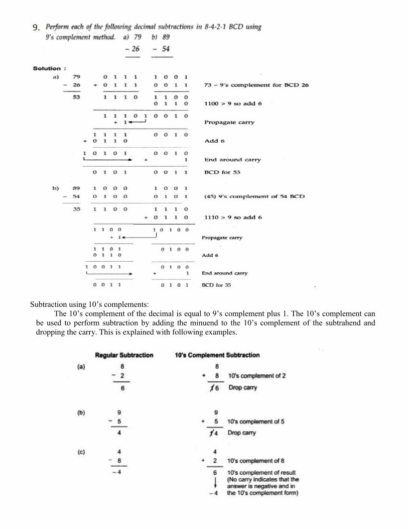
Subtraction using 10’s complements:
The 10’s complement of the decimal is equal to 9’s complement plus 1. The 10’s complement can be used to perform subtraction by adding the minuend to the 10’s complement of the subtrahend and dropping the carry. This is explained with following examples.

Steps for ’s o ple e t BCD su tra tio
1. Fi d the ’s o ple e t of a egative u er. 2. Add two numbers using BCD addition
3. If arry is ot ge erated fi d the ’s o ple e t of the result.
5.SIGNED NUMBERS
Digital systems like computer, must be able to handle both positive and negative numbers.
A signed binary number consists of both sign and magnitude information.
The sign indicates whether a number is positive or negative.
5.1 Representation
There are three forms in which the signed integer (whole numbers) can be represented. They
include,
1. Sign – Magnitude Form – Rarely used
2. 1’s Complement Form 3. 2’s Complement Form – Mostly used
Note:
Sign bit – leftmost bit in a signed binary numbers
0 for positive, 1 for negative
5.11 Sign Magnitude Form
Here, leftmost bit is the sign bit.
Remaining bits are magnitude bits.
Magnitude bits are in true binary.
5.12 1’s Complement Form
In this Form, positive numbers are represented the same way as positive sign-magnitude
numbers.

Negative numbers, are the 1’s complement of the corresponding positive numbers.
(eg)
+25 is represented as,
00011001 same as sign-magnitude form
-25 is represented as,
11100110 1’s complement of +25
5.13 2’s Complement Form
Positive numbers in 2’s complement form are represented as same as in sign-
magnitude and 1’s Complement Form. Negative numbers are the 2’s complement of the corresponding positive numbers
(eg)
+25 is represented as,
00011001 same as sign-magnitude form
-25 is represented as,
11100110 +
1 -------------------------------- 111001112 2’s complement of +25 -------------------------------
Decimal value of Signed Numbers
(1) Sign Magnitude
Decimal values of positive and negative numbers in this form are determined by
summing the weights in all the magnitude – bit positions.
The sign is determined by examining the sign bit.
(eg) 1. Determine the decimal value of this signed binary number expressed in sign –
magnitude. 10010101
Soln:
The seven magnitude bits and their powers of 2 weights are as follows.
1 0010101
26252423222120
Sign bit
Summing weights where there are 1’s. 16+4+1 = 21
Since, the sign bit is 1, the decimal number is -21

(2) 1’s Complement Decimal values of positive numbers in this form are determined by summing the
weights in all bit postions.
Decimal values of negative numbers are determined by assigning a negative value to
the weight of the sign bit, summing all the weights where there are 1’s and adding 1 to the result.
(eg) Determine the decimal value of the signed binary number expressed in 1’s complement 11101000
Soln:
The bits and their powers- of- two weights are as follows.
Note: for sign bit, it is -27 (or) -128
1 1 1 0 1 0 0 0
-27 26 25 24 23 22 21 20
Summing the weights where there are 1’s
-128+64+32+8 = -24 ( if +ve, write this as the result)
Since, it is a negative number, add 1 to the result
-24+1 = -23
(3) 2’s Complement Decimal values of positive and neagative numbers in this form are determined by
summing the weights in all bit positions.
The weight of the sign – bit in a negative number is given a negative value.
(eg): Determine the decimal values of the signed binary numbers expressed in 2’s complement from 10101010
Soln:
The bits and their corresponding powers of -2 weights are as follows
1 0 1 0 1 0 1 0
-27 26 25 24 23 22 21 20
Summing weights where there are 1’s
-128+32+8+2 = -86
Range of signed integer numbers that can be Represented
Since 8-bit (1byte) grouping is common in most computers, the illustrations are all 8-
bits. With 8-bits, we can represent 256 different numbers.
With 16-bits (2 bytes), we can represent 65,536 different numbers.
With 32-bits (4 bytes), we can represent 4.295×10⁹ different numbers.

The formula for finding the number of different combinations of n-bits is,
Total combinations = 2n
Range of values for n-bit numbers is,
-(2n-1) to + (2n-1 – 1)
So, for 8 bits the range is,
-128 to +127
For 16 bits the range is,
-32768 to +32767 etc
5.2 Arithmetic operations with Signed Numbers
Here, we use 2’s complement representation
Addition
The two numbers in an addition are the addend and the augend
The result is sum.
There are four cases that can occur when two signed binary numbers are added.
(1) Both numbers positive.
(2) Positive number with magnitude larger than negative number.
(3) Negative number with magnitude larger than positive number
(4) Both numbers negative.
Case 1: Both numbers +ve

Subtraction
It is a special case of addition.
The two numbers in subtraction are subtrahend and minuend.
The result is the difference.
To subtract +6 from +9, it is also equivalent to add -6 to +9.
So, to subtract two signed numbers, take the 2’s complement of the subtrahend and add. Discard any final carry bit.
6. BINARY ARITHMETIC 6.1 BINARY ADDITION
The binary addition table is as follows:
A+B SUM CARRY
0+0 0 0
0+1 1 0
1+0 1 0
1+1 0 1
Illustration 1:
Add (1010)2 and (0011)2
1010 (Augend) 0011 (Addend) ----------------------- 1101 (sum) -----------------------
The addition manipulated above as follows. Step 1: The least significant bits are added, i.e. 0+1 =1 with a carry of 0

Step 2: The carry in the previous is added to the next higher significant bits, i.e. 0+1+1= 0 with a carry 1. Step 3: The carry in the previous is added to the next higher significant bits, i.e. 1+0+0 =1 with a carry 0. Step 4: The preceding carry is added to the most significant bit i.e. 0+1+0 = 1 with a carry 0. Thus the sum is 1101.
6.2 BINARY SUBTRACTION
The binary subtraction table is as follows:
A-B DIFFERENCE BORROW
0-0 0 0
0-1 1 1
1-0 1 0
1-1 0 0
Illustration 1:
Subtract (0101)2 from (1011)2 1011 (Minuend) 0101 (Subtrahend) --------------------------- 0110 (Difference) ---------------------------
The steps are described below
Step1: the LSB in the first column are 1 and 1. Hence, the difference is 1 - 1 = 0 Step2: The column, the subtraction is performed as 1 – 0 = 1 Step3: In the third column, the difference is given by 0 – 1 =1 Step 4: In the fourth column (MSB), the difference is given by 0 – 0 = 0 since 1 is borrowed for third column.
6.3 BINARY MULTIPLICATION The binary multiplication table is as follows:
A *B PRODUCT
0 * 0 0
0 * 1 0
1 * 0 0
1 * 1 1
Binary multiplication uses add and shift process Binary multiplication is similar to decimal multiplication.
Illustration 1:
Multiplicand * Multiplier 10110.1x01001.1
---------------------------------- 101101 101101 000000 000000 101101 000000
---------------------------------- 011010101.11 (Final product)
----------------------------------- The steps are described below
Partial Product

Step 1: The LSB of the multiplier is taken. If multiplier bit is 1, the multiplicand is copied as such and if the multiplier bit is 0 zero is placed in all the bit positions. Step 2: The next higher significant bit of the multiplier is taken and, the partial product is written with the shift to the left, as in step 1. Step 3: step 2 is repeated for all other higher significant bits. Step 4: The partial product terms are added which gives the actual product of multiplier and the multiplicand.
6.4 BINARY DIVISION: The binary division table is as follows:
A÷B Result
0÷0 Not allowed
0÷1 0
1÷0 Not allowed
1÷1 1
Binary division uses subtract and shift process Binary division is similar to decimal division. Division by 0 is meaningless.
Illustration 1:
Dividend ÷ Divisor
11011.1÷ 101 101.1 (QUOTIENT)
DIVISOR 101 √11011.1 (DIVIDEND)
101 --------------
111 101
-------------- 101
101 --------------
0 --------------
7.BINARY CODES Binary codes are codes which are represented in binary system with modification from the original
one. The group of symbols is called as a code. The digital data is represented, stored and transmitted as group of binary bits. This group is also called as binary code. The binary code is represented by the number as well as alphanumeric letter. Advantages of Binary Code
Following is the list of advantages that binary code offers. 1. Binary codes are suitable for the computer applications. 2. Binary codes are suitable for the digital communications. 3. Binary codes make the analysis and designing of digital circuits if we use the binary codes. 4. Since only 0 and 1 are being used, implementation becomes easy.
7.1 Classification of binary codes:The codes are broadly categorized into following four categories.
Weighted Codes
Non-Weighted Codes
Binary Coded Decimal Code
Alphanumeric Codes

Error Codes 7.1.1 Weighted codes: Weighted binary codes are those binary codes which obey the positional weight principle. Each position of the number represents a specific weight
Decimal 8421 5421 2421 5211
0 0000 0000 0000 0000
1 0001 0001 0001 0001
2 0010 0010 0010 0011
3 0011 0011 0011 0101
4 0100 0100 0100 0111
5 0101 1000 1011 1000
6 0110 1001 1100 1010
7 0111 1010 1101 1100
8 1000 1011 1110 1110
9 1001 1100 1111 1111
For example, in 8421BCD code, 1001 the weights of 1, 0, 0, 1 (from left to right) are 8, 4, 2 and 1 respectively. The codes 8421BCD, 2421BCD, 5211BCD are all weighted codes. 7.1.2 Non-weighted codes: The non-weighted codes are not positionally weighted. In other words, each digit position within the number is not assigned a fixed value (or weight). Examples are
Excess-3
Gray code DECIMAL EXCESS - 3 GRAY CODE
0 0011 0000
1 0100 0001
2 0101 0011
6.1.3 EXCESS – 3 CODES:-
This is another form of BCD code, in which each decimal digit is coded into a 4-bit binary code.
The code for each decimal digit is obtained by adding decimal 3 to the natural BCD code of the digit.
GRAY CONVERSION:-
Record the mostsignificant bit add the binary MSB to the next significant bit of the Gray code.
Record the result, ignoring carrier continue the process, until the LSB is reached. REFLECTIVE CODES: A code is reflective when the code is self-complementing. In otherwords, when the code for 9 is the complement the code for 0, 8 for 1, 7 for 2, 6 for 3 and 5 for 4. 2421BCD, 5421BCD and Excess-3 code are reflective codes. SEQUENTIAL CODES: In sequential codes, each succeeding 'code is one binary number greater than its preceding code. This property helps in manipulation of data. 8421 BCD and Excess-3 are sequential codes. ALPHANUMERIC CODES: Codes used to represent numbers, alphabetic characters, symbols and various instructions necessary for conveying intelligible information. ASCII, EBCDIC, UNICODE are the most-commonly used alphanumeric codes.
8.Decimal code Binary codes for decimal digits require a minimum of four bits. Numerous different codes can be obtained by arranging four or more bits in ten distinct possible combinations. A few possibilities are tabulated.

9.Error detection code In data transmission, Interference and physical defects in the communication medium can cause random bit errors. As the signal is transmitted through a media, the signal gets corrupted because of noise and distortion. Therefore the media is not reliable. To achieve a reliable communication through this unreliable media, there is need for detecting the error in the signal so that suitable mechanism can be devised to take corrective actions. Error coding is a method of detecting and correcting these errors to ensure information is transferred intact from its source to its destination The errors can be divided into two types: • Single-bit Error: only one bit of given data unit (such as a byte, character, or data unit) is changed from 1 to 0 or from 0 to 1. • Burst Error: two or more bits in the data unit have changed from 0 to 1 or vice-versa. (Here doesn’t necessary means that error occurs in consecutive bits) Error Detecting Codes: Basic approach used for error detection is the use of redundancy, where additional bits are added to facilitate detection and correction of errors. Popular techniques are: • Simple Parity check • Two-dimensional Parity check • Checksum • Cyclic redundancy check Detecting Errors using simple parity check
Suppose we are transmitting 7-bit ASCII characters. A parity bit is added to each character to make it 8 bits. Parity can detect all single-bit errors –If even parity is used and a single bit changes, it will change the parity to odd, which will be detected at the receiver end –The receiver end can detect the error, but cannot correct it because it does not know which bit is erroneous Parity can also detect some multiple-bit errors Table 1 shows the four bit data word and its corresponding code words
Decimal value Data block Parity bit Code word
0 0000 0 00000
1 0001 1 00011
2 0010 1 00101

3 0011 0 00110
4 0100 1 01001
5 0101 0 01010
6 0110 0 01100
7 0111 1 01111
8 1000 1 10001
9 1001 0 10010
10 1010 0 10100
11 1011 1 10111
12 1100 0 11000
13 1101 1 11011
14 1110 1 11101
15 1111 0 11110
10.Gray Code- Reflection and Self Complementary codes Gray Code is a non-weighted code which belongs to a class of codes called minimum change codes.
Gray Code is an alternative binary representation, devised such that, between any two adjacent numbers, only one bit changes at a time.
Binary Dec Gray
00000 0 00000
00001 1 00001
00010 2 00011
00011 3 00010
00100 4 00110
00101 5 00111
00110 6 00101
00111 7 00100
01000 8 01100
01001 9 01101
01010 10 01111
01011 11 01110
01100 12 01010
01101 13 01011
01110 14 01001
01111 15 01000
To the left we see three columns of data. These are representations of the same numbers 0-15 in different ways.
o In the middle is the decimal value. o On the left is positional notation binary o On the right is Gray code.
You will notice that, on the right, each adjacent row is different from it's neighbours by no more than one bit.
The term Gray code is often used to refer to a "reflected" code, or more specifically still, the binary reflected Gray code.
10.1 Self-complementary Code

• A code is said to be self-complementary if the code for 9’s complement of N i.e. 9-N can be obtained by interchanging all 0s and 1s. • Decimal 9 is the complement of code for 0, 8 for 1, 7 for 2 and so on. • For a code to be self complementing, the sum of all its weights must be 9. digit.8421 and 5421 codes are not self complementing codes whereas 5211,2421,3321, 4321 are self complementing. • In general, a code is self-complementary if we produce a code by taking the first complement of the digit which is same as 9’s complement of the number.
10.2 Reflective code
Imaged about the centre entries with one bit changed
Example ï 9ís complement of a reflected BCD code word is formed by changing only one of its bits
In the Gray code example shown below, the MSB bit alone is changing and the remaining bits is reflected mirror image about the centre. For clarity, the MSB is removed.
Gray code Reflected property of Gray code
Binary-to-Gray code conversion
The MSB in the Gray code is the same as corresponding MSB in the binary number.
Going from left to right, add each adjacent pair of binary code bits to get the next Gray code bit.
Discard carries. Problem: Convert 10110 to gray code
Gray-to-Binary Conversion
The MSB in the binary code is the same as the corresponding bit in the Gray code.
Add each binary code bit generated to the Gray code bit in the next adjacent position.
Discard carries. Problem: Convert the Gray code word 11011 to binary

11. Binary-Coded Decimal Code Although the binary number system is the most natural system for a computer because it is readily
represented in today’s electronic technology, most people are more accustomed to the decimal system. One way to resolve this difference is to convert decimal numbers to binary, perform all arithmetic calculations in binary, and then convert the binary results back to decimal. This method requires that we store decimal numbers in the computer so that they can be converted to binary. Since the computer can accept only binary values, we must represent the decimal digits by means of a code that contains 1’s and 0’s. It is also possible to perform the arithmetic operations directly on decimal numbers when they are stored in the computer in coded form.
A binary code will have some unassigned bit combinations if the number of elements in the set is not a multiple power of 2. The 10 decimal digits form such a set. A binary code that distinguishes among 10 elements must contain at least four bits, but 6 out of the 16 possible combinations remain unassigned. Different binary codes can be obtained by arranging four bits into 10 distinct combinations. This scheme is called binary-coded decimal and is commonly referred to as BCD.
A number with k decimal digits will require 4k bits in BCD. Decimal 396 is represented in BCD with 12 bits as 0011 1001 0110, with each group of 4 bits representing one decimal digit. A decimal number in BCD is the same as its equivalent binary number only when the number is between 0 and 9. A BCD number greater than 10 looks different from its equivalent binary number, even though both contain 1’s and 0’s. Note that the BCD code is not self‐complementing. Moreover, the binary combinations 1010 through 1111 are not used and have no meaning in BCD. Consider decimal 185 and its corresponding value in BCD and binary: (185)10 = (0001 1000 0101) BCD = (10111001)2
Table 1 In multi digit BCD coding
11.1 BCD addition:
The addition of two BCD numbers can be best understood by considering the three cases that occur when two BCD digits are added. Sum equals 9 or less with carry 0
Let us consider additions of 3 and 6 in BCD.

Sum greater than 9 with carry 0
Let us consider addition of 6 and 8 in BCD
The sum 1110 is an invalid BCD number. This has occurred because the sum of the two digits exceeds 9. Whenever this occurs this occurs the sum has to be corrected by the addition of six (1110) in the invalid BCD number, as shown below
Sum equals 9 or less with carry 1
Let us consider addition of 8 and 9 in BCD
In this case, result (001 0001) is valid BCD number, but it is incorrect. To get the correct BCD result correction factor of 6 has to be added to the least significant digit sum, as shown.
BCD addition procedure
1. Add two BCD numbers using ordinary binary addition. 2. If four bit sum is equal to or less than 9, no correction is needed. The sum is in proper BCD form.

3. If the four bit sum is greater than 9 or if a carry is generated from the four-bit sum, the sum is invalid.
4. To correct the invalid sum, add 01102 to the four-bit sum. If a carry results from this addition, add it to the next higher-order BCD digit.
12.Alphanumeric codes Alphanumeric codes are sometimes called character codes due to their certain properties. Now
these codes are basically binary codes. We can write alphanumeric data, including data, letters of the alphabet, numbers, mathematical symbols and punctuation marks by this code which can be easily understandable and can be processed by the computers. Input output devices such as keyboards, monitors, mouse can be interfaced using these codes. 12-bit Hollerith code is the better known and perhaps the first effective code in the days of evolving computers in early days. During this period punch cards were used as the inputting and outputting data. But nowadays these codes are termed obsolete as many other modern codes have evolved. The most common alphanumeric codes used these days are ASCII code, EBCDIC
code and Unicode.
12.1 ASCII Character Code

Many applications of digital computers require the handling not only of numbers, but also of other characters or symbols, such as the letters of the alphabet. For instance, consider a high‐tech company with thousands of employees. To represent the names and other pertinent information, it is necessary to formulate a binary code for the letters of the alphabet. In addition, the same binary code must represent numerals and special characters (such as $). An alphanumeric character set is a set of elements that includes the 10 decimal digits, the 26 letters of the alphabet, and a number of special characters. Such a set contains between 36 and 64 elements if only capital letters are included, or between 64 and 128 elements if both uppercase and lowercase letters are included. In the first case, we need a binary code of six bits, and in the second, we need a binary code of seven bits. The standard binary code for the alphanumeric characters is the American Standard Code for Information Interchange (ASCII), which uses seven bits to code 128 characters, as shown in Table below. The seven bits of the code are designated by b1 through b7, with b7 the most significant bit. The letter A, for example, is represented in ASCII as 1000001 (column 100, row 0001). The ASCII code also contains 94 graphic characters that can be printed and 34 nonprinting characters used for various control functions.
The graphic characters consist of the 26 uppercase letters (A through Z), the 26 lowercase letters (a through z), the 10 numerals (0 through 9), and 32 special printable characters, such as %, *, and $.characters. Format effectors are characters that control the layout of printing. They include the familiar word processor and typewriter controls such as backspace (BS), horizontal tabulation (HT), and carriage return (CR). Information separators are used to separate the data into divisions such as paragraphs and pages. They include characters such as record separator (RS) and file separator (FS). The communication‐control characters are useful during the transmission of text between remote devices so that it can be distinguished from other messages using the same communication channel before it and after it. Examples of communication‐control characters are STX (start of text) and ETX (end of text), which are used to frame a text message transmitted through a communication channel.
ASCII is a seven‐bit code, but most computers manipulate an eight‐bit quantity as a single unit called a byte. Therefore, ASCII characters most often are stored one per byte. The extra bit is sometimes used for other purposes, depending on the application.
For example, some printers recognize eight‐bit ASCII characters with the most significant bit set to 0. An additional 128 eight‐bit characters with the most significant bit set to 1 are used for other symbols, such as the Greek alphabet or italic type font.
12.2 EBCDIC

The EBCDIC stands for Extended Binary Coded Decimal Interchange Code. IBM invented this code to extend the Binary Coded Decimal which existed at that time. All the IBM computers and peripherals use this code. It is an 8 bit code and therefore can accommodate 256 characters. Below is given some characters of EBCDIC code to get familiar with it.
13. HAMMING CODE-ERROR DETECTION AND CORRECTION
Hamming code is a set of error-correction code s that can be used to detect and correct bit errors
that can occur when computer data is moved or stored. 13.1 Error Detecting Codes
Basic approach used for error detection is the use of redundancy, where additional bits are added to facilitate detection and correction of errors. Popular techniques are: • Simple Parity check • Two-dimensional Parity check • Checksum • Cyclic redundancy check Simple Parity Checking or One-dimension Parity Check The most common and least expensive mechanism for error- detection is the simple parity check. In this technique, a redundant bit called parity bit, is appended to every data unit so that the number of 1s in the unit (including the parity becomes even). Blocks of data from the source are subjected to a check bit or Parity bit generator form, where a parity of 1 is added to the block if it contains an odd number of 1’s (ON bits) and 0 is added if it contains an even number of 1’s. At the receiving end the parity bit is computed from the received data bits and compared with the received parity bit, as shown in Fig 1. This scheme makes the total number of 1’s even, that is why it is called even parity checking. Considering a 4-bit word, different combinations of the data words and the corresponding code words are given in Table 1. Note that for the sake of simplicity, we are discussing here the even-parity checking, where the number of 1’s should be an even number. It is also possible to use odd-parity checking, where the number of 1’s should be odd.

Fig 1) Even parity checking scheme
Table 1:Possible 4 bit data words and corresponding code words
Two-dimension Parity Check Performance can be improved by using two-dimensional parity check, which organizes the block of bits in the form of a table. Parity check bits are calculated for each row, which is equivalent to a simple parity check bit. Parity check bits are also calculated for all columns then both are sent along with the data. At the receiving end these are compared with the parity bitcalculated on the received data. This is illustrated in Fig. 2. Performance Two- Dimension Parity Checking increases the likelihood of detecting burst errors. As we have shown in Fig. 2, that a 2-D Parity check of n bits can detect a burst error of n bits. A burst error of more than n bits is also detected by 2-D Parity check with a highprobability. There is, however, one pattern of error that remains elusive. If two bits in one data unit are damaged and two bits in exactly same position in another data unit are also damaged, the 2-D Parity check checker will not detect an error. For example, if two data units: 11001100 and 10101100. If first and second from last bits in each of them is changed, making the data units as 01001110 and 00101110, the error cannot be detected by 2-D Parity check.

Fig 2) Two dimension parity checking Example of Hamming Code Generation
Suppose a binary data 1001101 is to be transmitted. To implement hamming code for this, following steps are used: 1. Calculating the number of redundancy bits required. Since number of data bits is 7, the value of r is calculated as
2r > m + r + 1 24 > 7 + 4 + 1
Therefore no. of redundancy bits = 4 2. Determining the positions of various data bits and redundancy bits. The various r bits are placed at the position that corresponds to the power of 2 i.e. 1, 2, 4, 8

4. Thus data 1 0 0 1 1 1 0 0 1 0 1 with be transmitted. 13.1 Error Detection & Correction
Considering a case of above discussed example, if bit number 7 has been changed from 1 to 0.The data will be erroneous.
Data sent: 1 0 0 1 1 1 0 0 1 0 1 Data received: 1 00 1 0 1 00 1 0 1 (seventh bit changed) The receive takes the transmission and recalculates four new VRCs using the same set of bits used by sender plus the relevant parity (r) bit for each set as shown in fig. Then it assembles the new parity values into a binary number in order of r position (r8, r4, r2, r1). In this example, this step gives us the binary number 0111. This corresponds to decimal 7. Therefore bit number 7 contains an error. To correct this error, bit 7 is reversed from 0 to 1.
References :
1. Moris Mano, “Digital Computer Fundamentals” TMH 3rd Edition 2. http://www.tutorialspoint.com/computer_logical_organization/number_system_conversion.htm 3. http://www.electronics-tutorials.ws/binary/signed-binary-numbers.html 4. HAMMING, R. →. “Error Detecting and Error Correcting Codes.” Bell System Tech. Jour., 29
(1950): 147–160. 5. A.P GODSE,D.A.GODSE .”Digital Systems”.Technical Publications.Pune. 6. http://www.tutorialspoint.com/computer_logical_organization/binary_codes.htm 7. http://nptel.ac.in/courses/Webcourse-
contents/IIScBANG/Digital%20Systems/Digital%20Systems.pdf 8. Digital Logic Circuits by D.A.Godse A.P.Godse

SCHOOL OF ELECTRICAL AND ELECTRONICS
DEPARTMENT OF ELECTRICAL AND ELECTRONICS
UNIT –II- BOOLEAN ALGEBRA AND LOGIC GATES
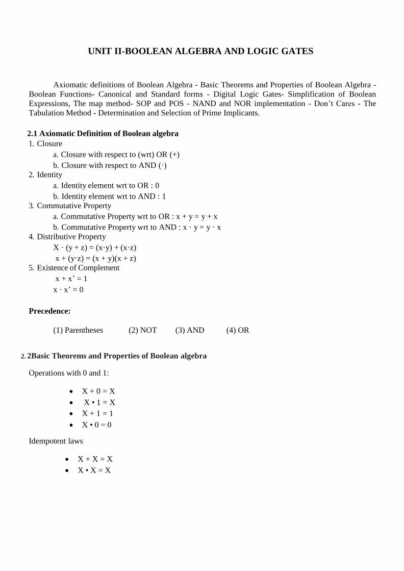
UNIT II-BOOLEAN ALGEBRA AND LOGIC GATES
Axiomatic definitions of Boolean Algebra - Basic Theorems and Properties of Boolean Algebra -
Boolean Functions- Canonical and Standard forms - Digital Logic Gates- Simplification of Boolean
Expressions, The map method- SOP and POS - NAND and NOR implementation - Don’t Cares - The
Tabulation Method - Determination and Selection of Prime Implicants.
2.1 Axiomatic Definition of Boolean algebra
1. Closure
a. Closure with respect to (wrt) OR (+)
b. Closure with respect to AND (·)
2. Identity
a. Identity element wrt to OR : 0
b. Identity element wrt to AND : 1
3. Commutative Property
a. Commutative Property wrt to OR : x + y = y + x
b. Commutative Property wrt to AND : x · y = y · x
4. Distributive Property
X · (y + z) = (x·y) + (x·z)
x + (y·z) = (x + y)(x + z)
5. Existence of Complement
x + x’ = 1
x · x’ = 0
Precedence:
(1) Parentheses (2) NOT (3) AND (4) OR
2. 2Basic Theorems and Properties of Boolean algebra
Operations with 0 and 1:
X + 0 = X
X • 1 = X
X + 1 = 1
X • 0 = 0
Idempotent laws
X + X = X
X • X = X

Involution law:
( X' ) ' = X
Laws of complementarity:
X + X' = 1
X • X' = 0
Commutative laws:
X + Y = Y + X
X • Y = Y • X
Associative laws:
(X + Y) + Z = X + (Y + Z) = X + Y + Z
(XY)Z = X(YZ) = XYZ
Distributive laws:
X( Y + Z ) = XY + XZ
X + YZ = ( X + Y ) ( X + Z )
Simplification theorems:
X Y + X Y' = X
( X + Y ) ( X + Y' ) = X
X + XY = X
X ( X + Y ) = X
( X + Y' ) Y = XY
XY' + Y = X + Y
DeMorgan’s laws:
There are two “de Morgan´s” rules or theorems,
Two separate terms NOR´ed together is the same as the two terms inverted (Complement)
and AND´ed for example, (X+Y)’ = X’.Y’.
Two separate terms NAND´ed together is the same as the two terms inverted (Complement)
and OR´ed for example, (X.Y)’ =X’ +Y’.
Duality:
“Every algebraic expression deducible from the postulates of Boolean Algebra remains valid if the
operations and identity elements are interchanged.”
( X + Y + Z + … ) D = X Y Z …
(X Y Z…) D = X + Y + Z + …
[ f ( X1, X2, … XN, 0, 1, +, • ) ] D = f ( X1, X2, … XN, 1, 0, •, + )

3. Boolean Functions
A simple 2-input AND, OR and NOT Gates can be represented by 16 possible functions as shown in the
following table.
3.1 Laws of Boolean Algebra
Function Description Expression
1. NULL 0
2. IDENTITY 1
3. Input A A
4. Input B B
5. NOT A A’
6. NOT B B’
7. A AND B (AND) A . B
8. A AND NOT B A . B’
9. NOT A AND B A’ . B
10. NOT A AND NOT B (NAND) A’ . B’
11. A OR B (OR) A + B
12. A OR NOT B A + B’
13. NOT A OR B A’ + B
14. NOT OR (NOR) (A + B)’
15. Exclusive-OR A.B’ + A’.B
16. Exclusive-NOR A’.B’ + A.B
Example
Using the above laws, simplify the following expression: (A + B)(A + C)
Q = (A + B).(A + C)
A.A + A.C + A.B + B.C – Distributive law
A + A.C + A.B + B.C – Idempotent AND law (A.A = A)
A(1 + C) + A.B + B.C – Distributive law
A.1 + A.B + B.C – Identity OR law (1 + C = 1)
A(1 + B) + B.C – Distributive law
A.1 + B.C – Identity OR law (1 + B = 1)
Q = A + (B.C) – Identity AND law (A.1 = A)
Then the expression: (A + B)(A + C) can be simplified to A + (B.C) as in the Distributive law.
4. Canonical and Standard Forms
Logical functions are generally expressed in terms of different combinations of logical variables with
their true forms as well as the complement forms. Binary logic values obtained by the logical functions
and logic variables are in binary form. An arbitrary logic function can be expressed in the following
forms.
(i) Sum of the Products (SOP)
(ii) Product of the Sums (POS)
Product Term:

In Boolean algebra, the logical product of several variables on which a function depends is
considered to be a product term. In other words, the AND function is referred to as a product term
or standard product. The variables in a product term can be either in true form or in
complemented form. For example, ABC′ is a product term.
Sum Term:
An OR function is referred to as a sum term. The logical sum of several variables on which
a function depends is considered to be a sum term. Variables in a sum term can also be either in
true form or in complemented form. For example, A + B + C′ is a sum term.
Sum of Products (SOP):
The logical sum of two or more logical product terms is referred to as a sum of products
expression. It is basically an OR operation on AND operated variables. For example, Y = AB +
BC + AC or Y = A′B + BC + AC′ are sum of products expressions.
Product of Sums (POS):
Similarly, the logical product of two or more logical sum terms is called a product of sums
expression. It is an AND operation on OR operated variables. For example, Y = (A + B + C)(A +
B′ + C)(A + B + C′) or Y = (A + B + C)(A′ + B′ + C′) are product of sums expressions.
Standard form:
The standard form of the Boolean function is when it is expressed in sum of the products
or product of the sums fashion. The examples stated above, like Y =AB + BC + AC or Y = (A +
B + C)(A + B′ + C)(A + B + C′) are the standard forms. However, Boolean functions are also
sometimes expressed in nonstandard forms like F = (AB + CD)(A′B′ + C′D′), which is neither a
sum of products form nor a product of sums form. However, the same expression can be
converted to a standard form with help of various Boolean properties, as:
F = (AB + CD)(A′B′ + C′D′) = A′B′CD + ABC′D′
4.1 Minterm
A product term containing all n variables of the function in either true or complemented
form is called the minterm. Each minterm is obtained by an AND operation of the variables in
their true form or complemented form. For a two-variable function, four different combinations
are possible, such as, A′B′, A′B, AB′, and AB. These product terms are called the fundamental
products or standard products or minterms. In the minterm, a variable will possess the value 1 if it
is in true or uncomplemented form, whereas, it contains the value 0 if it is in complemented form.
For three variables function, eight minterms are possible as listed in the following table
A B C Minterm
0 0 0 A’B’C’
0 0 1 A’B’C
0 1 0 A’BC’
0 1 1 A’BC
1 0 0 AB’C’
1 0 1 AB’C
1 1 0 ABC’
1 1 1 ABC
So, if the number of variables is n, then the possible number of minterms is 2n. The main property
of a minterm is that it possesses the value of 1 for only one combination of n input variables and
the rest of the 2n – 1 combinations have the logic value of 0. This means, for the above three
variables example, if A = 0, B = 1, C = 1 i.e., for input combination of 011, there is only one
combination A′BC that has the value 1, the rest of the seven combinations have the value 0.
Canonical Sum of Product Expression:
When a Boolean function is expressed as the logical sum of all the minterms from the rows
of a truth table, for which the value of the function is 1, it is referred to as the canonical sum of
product expression. The same can be expressed in a compact form by listing the corresponding
decimal-equivalent codes of the minterms containing a function value of 1.
For example, if the canonical sum of product form of a three-variable logic function F has
the minterms A′BC, AB′C, and ABC′, this can be expressed as the sum of the decimal codes
corresponding to these minterms as below.
F (A,B,C) = (3,5,6)
= m3 + m5 + m6
= A′BC + AB′C + ABC′
where Σ (3,5,6) represents the summation of minterms corresponding to decimal codes 3, 5, and
6. The canonical sum of products form of a logic function can be obtained by using the following
procedure:
1. Check each term in the given logic function. Retain if it is a minterm, continue to examine the
next term in the same manner.
2. Examine for the variables that are missing in each product which is not a minterm. If the
missing variable in the minterm is X, multiply that minterm with (X+X′).
2. Multiply all the products and discard the redundant terms.
4.2 Maxterm
A sum term containing all n variables of the function in either true or complemented form
is called the maxterm. Each maxterm is obtained by an OR operation of the variables in their true
form or complemented form. Four different combinations are possible for a two-variable function,
such as, A′ + B′, A′ + B, A + B′, and A + B. These sum terms are called the standard sums or
maxterms. Note that, in the maxterm, a variable will possess the value 0, if it is in true or
uncomplemented form, whereas, it contains the value 1, if it is in complemented form. Like
minterms, for a three-variable function, eight maxterms are also possible as listed in the following
table

A B C Maxterm
0 0 0 A+B+C
0 0 1 A+B+C’
0 1 0 A+B’+C
0 1 1 A+B’+C’
1 0 0 A’+B+C
1 0 1 A’+B+C’
1 1 0 A’+B’+C
1 1 1 A’+B’+C’
So, if the number of variables is n, then the possible number of maxterms is 2n. The main
property of a maxterm is that it possesses the value of 0 for only one combination of n input
variables and the rest of the 2n –1 combinations have the logic value of 1. This means, for the
above three variables example, if A = 1, B = 1, C = 0 i.e., for input combination of 110, there is
only one combination A′ + B′ + C that has the value 0, the rest of the seven combinations have
the value 1.
Canonical Product of Sum Expression:
When a Boolean function is expressed as the logical product of all the maxterms from the rows of
a truth table, for which the value of the function is 0, it is referred to as the canonical product of
sum expression. The same can be expressed in a compact form by listing the corresponding
decimal equivalent codes of the maxterms containing a function value of 0. For example, if the
canonical product of sums form of a three-variable logic function F has the maxterms A + B + C,
A + B′ + C, and A′ + B + C′, this can be expressed as the product of the decimal codes
corresponding to thesemaxterms as below,
F (A,B,C) = Π (0,2,5)
= M0 M2 M5
= (A + B + C) (A + B′ + C) (A′ + B + C′)
where Π (0,2,5) represents the product of maxterms corresponding to decimal codes 0, 2, and 5.
The canonical product of sums form of a logic function can be obtained by using the following
procedure.
1. Check each term in the given logic function. Retain it if it is a maxterm, continue to examine
the next term in the same manner.
2. Examine for the variables that are missing in each sum term that is not a maxterm. If the
missing variable in the maxterm is X, add that maxterm with (X.X′).
3. Expand the expression using the properties and postulates as described earlier and discard the
redundant terms. Some examples are given here to explain the above procedure.
5. Boolean Function

Boolean algebra deals with binary variables and logic operation. A Boolean Function is described by an
algebraic expression called Boolean expression which consists of binary variables, the constants 0 and 1, and the
logic operation symbols. Consider the following example
5.1 Truth Table Formation A truth table represents a table having all combinations of inputs and their corresponding result.
It is possible to convert the switching equation into a truth table. For example, consider the following switching equation.
The output will be high (1) if A = 1 or BC = 1 or both are 1. The truth table for this equation is shown by Table (a).
The number of rows in the truth table is 2nwhere n is the number of input variables (n=3 for the given equation).
Hence there are 23 = 8 possible input combination of inputs.
6. DIGITAL LOGIC GATES
A large number of electronic circuits (in computers, control units, and so on) are made up of logic
gates.Digital systems are said to be constructed by using logic gates. These process signals which represent true
or false. The basic gates are the AND, OR, NOT gates. The most common symbols used to represent logic gates are
shown below.
AND gate:

The AND gate is an electronic circuit that gives a high output (1) only if all its inputs are high. A dot (.) is
used to show the AND operation i.e. A.B. Bear in mind that this dot is sometimes omitted i.e. AB. OR gate:
The OR gate is an electronic circuit that gives a high output (1) if one or more of its inputs are high. A
plus (+) is used to show the OR operation.
NOT gate:
7. Simplification of Boolean Expressions
Minimization of Boolean functions is an approach where a given Boolean expression can be transformed
from one form to another equivalent form by applying Boolean Theorems. By minimizing the expressions the individual components used in electrical circuits can be minimized or reduced. This allows designers to make use of fewer components, thus reducing the cost of a particular system. It should be noted that there are no fixed rules that can be used to minimize a given expression. It is left to an individual’s ability to apply Boolean Theorems in order to minimize a function.
Examples:
Example 1:
Using Boolean algebra techniques, simplify the expression X . Y + X (Y + Z) + Y (Y + Z)
Solution:
Given: X . Y + X (Y + Z) + Y (Y + Z). Applying distributive property, we get X . Y + X (Y + Z) + Y (Y + Z) = X . Y + X . Y + X . Z + Y . Y + Y . Z
We know B . B = B = X . Y + X . Y + X . Z + Y + Y . Z
We know A . B + A . B = A . B = X . Y + X . Z + Y + Y . Z = X . Y + X . Z + Y [We know (B + BC = B)] = Y + XZ

Example 2:
Using Boolean algebra techniques, simplify this expression: AB + A(B + C) + B(B + C)
Solution Apply the distributive law to the second and third terms in the expression, as follows: AB + A(B + C) + B(B + C)=AB + AB + AC + BB + BC =AB + AB + AC + B + BC
[BB = B] =AB + AC + B + BC [AB + AB = AB] =AB + AC + B [B + BC = B] =B+AC
[AB + B = B] Example 3:
Using Boolean algebra techniques, simplify this expression A.B’ + A.B + B.C
Solution
A.B’ + A.B + B.C= A. (B’ + B) + B.C
= A.1 + B.C = A + B.C
Example 4:
Using Boolean algebra techniques, simplify this expression A’.B.C + A.B’.C + A.B.C’ + A.B.C
Solution: A’.B.C + A.B’.C + A.B.C’ + A.B.C = A’.B.C + A.B’.C + A.B.C’ + A.B.C + A.B.C + A.B.C
= (A’.B.C + A.B.C) + (A.B’.C + A.B.C) + (A.B.C’ + A.B.C) = (A’ + A). B.C + (B’ + B). C.A + (C’ + C). A.B = B.C + C.A + A.B
7.1 STANDARD FORMS OF BOOLEAN EXPRESSIONS
All Boolean expressions, regardless of their form, can be converted into either of two standard forms: the sum-of-products form or the product-of-sums form.
Standardization makes the evaluation, simplification, and implementation of Boolean expressions much
more systematic and easier.
7.1.1 The Sum-of-Products (SOP) Form
When two or more product terms are summed by Boolean addition, the resulting expression is a sum-of-products (SOP). Some examples are:
AB + ABC ABC + C’DE + B’CD’ AB + BCD + AC
Also, an SOP expression can contain a single-variable term, as in A + ABC’ + BCD’.
In an SOP expression a single over bar cannot extend over more than one variable.
Example

Convert each of the following Boolean expressions to SOP form: (a) AB + B(CD + EF) (b) (A + B)(B + C + D) (c) *(A + B)’ + C+’
The Standard SOP Form
So far, you have seen SOP expressions in which some of the product terms do not contain all of the
variables in the domain of the expression. For example, the expression A’BC’ + AB’D + ABC’D’ has a domain made up of the variables A, B, C. and D.
However, notice that the complete set of variables in the domain is not represented in the first two terms of the expression; that is, D or D’ is missing from the first term and C or C’ is missing from the second term.
A standard SOP expression is one in which all the variables in the domain appear in each product term in the expression. For example, A’BCD’ + ABC’D+ AB’CD are a standard SOP expression.
Converting Product Terms to Standard SOP:
Each product term in an SOP expression that does not contain all the variables in the domain can be
expanded to standard SOP to include all variables in the domain and their complements. As stated in the
following steps, a nonstandard SOP expression is converted into standard form using Boolean algebra rule
(A + A’ = 1) i.e., A variable added to its complement equals 1.
Step 1: Multiply each nonstandard product term by a term made up of the sum of a missing variable and
its complement. This results in two product terms. As you know, you can multiply anything by 1 without changing its Value.
Step 2: Repeat Step 1 until all resulting product terms contain all variables in the domain in either
complemented or uncomplemented form. In converting a product term to standard form, the number of product terms is doubled for each missing variable. Example Convert the following Boolean expression into standard SOP form: AB’C + A’B’ + ABC’D
Solution
The domain of this SOP expression A, B, C, D. Take one term at a time.
The first term, ABC, is missing variable D or D’, so multiply the first term by(D + D) as follows: AB’C =
AB’C(D + D’) = AB’CD + AB’CD’ In this case, two standard product terms are the result.
The second term, A’B’; is missing variables C or C’ and D or D’, so first multiply the second term by C + C’ as follows:
A’B’ = A’B’(C + C’) = A’B’C + A’B’C’
The two resulting terms are missing variable D or D’, so multiply both terms by (D + D) as follows A’B’C(D + D’) + A’B’C’(D + D’)= A’B’CD + A’B’CD’ + A’B’C’D + A’B’C’D’ In this case, four standard product terms are the result.
The third term, ABC’D, is already in standard form. The complete standard SOP form of the original expression is as follows:
AB’C + A’B’ + ABC’D = AB’CD + AB’CD ‘+ A’ B’CD + A’B’CD’ + A’B’C’D +A’B’C’D’ + ABC’D
7.1.2 The Product-of-Sums (POS) Form
A sum term was defined before as a term consisting of the sum (Boolean addition) of literals (variables or

their complements). When two or more sum terms are multiplied, the resulting expression is a product-of-sums (POS). Some examples are
(A’ + B)(A + B’ + C) (A + B’ + C’)( C + D’ + E)(B + C + D) (A + B’)(A + B’ + C)(A + C)
A POS expression can contain a single-variable term, as inA(A + B + C)(B + C + D).
In a POS expression, a single over bar cannot extend over more than one variable; however, more than
one variable in a term can have an over-bar. For example, a POS expression can have the term A’ + B’ + C’ but not *A + B + C+’.
Implementation of a POS Expression simply requires ANDing the outputs of two or more OR gates. A sum
term is produced by an OR operation and the product of two or more sum terms is produced by an AND operation.
The Standard POS Form
So far, you have seen POS expressions in which some of the sum terms do not contain all of the variables
in the domain of the expression. For example, the expression(A’ + B + C) (A + B + D’) (A + B’ + C’ + D)has a domain made up of the variables
A, B, C, and D. Notice that the complete set of variables in the domain is not represented in e first two terms of the expression; that is, D or D’ is missing from the first term and C or C’ is missing from the second term.
A standard POS expression is one in which all the variables in the domainappear in each sum term in the
expression. For example,(A’ + B’ + C + D)(A + B’ + C + D)(A + B + C + D)is a standard POS expression. Converting a Sum Term to Standard POS
Each sum term in a POS expression that does not contain all the variables in the domain can be expanded
to standard form to include all variables in the domain and their complements. As stated in the following steps, a
Nonstandard POS expression is converted into standard form using Boolean algebra rule
(A’. A = 0) i.e., A
variable multiplied to its complement equals 0.
Step 1. Add to each nonstandard product term a term made up of the product of the missing variable and its complement. This results in two sum terms. As you know, you can add 0 to anything without changing its value.
Step 2. Apply rule A + BC = (A + B)(A + C).
Step 3. Repeat Step 1 until all resulting sum terms contain all variables in the domain in either
complemented or non-complemented form. Example
Convert the following Boolean expression into standard POS form:(A’ + B + C)(B’ + C + D’)(A + B’ + C’ + D)
Solution
The domain of this POS expression is A, B, C, D. Take one term at a time.
The first term, A + B + C, is missing variable D or D’, so add D’D and apply rule as follows: A’ + B +
C = A’ + B + C + D’D = (A’ + B + C + D’)(A’ + B + C + D)
The second term, B’ + C + D’, is missing variable A or A’, so add A’A andapply rule as follows: B’ + C +
D’ = B’ + C + D’ + A’A

= (A’ + B’ + C + D’)(A + B’ + C + D’) The third term, A + B’ + C’ + D, is already in standard form. The standardPOS form of the original
expression is as follows: (A’ + B + C)(B’ + C + D’)(A + B’ + C’ + D) = (A’ + B + C + D’)(A’ + B + C +D) (A’ + B’ + C + D’)(A + B’ + C + D’) (A + B’ + C’ + D) 7.2 CANONICAL FORMS OF BOOLEAN EXPRESSIONS
With one variable x & x. With two variables x y, x y, x y and x y. With three variables x’ y’ z’, x’ y’ z, x’ y z’, x’ y z, x y’ z’, x y’ z, x y z’ & x y z.
These eight AND terms are called Minterms.
1 0 0 XY’Z’ m4
1 0 1 XY’Z m5
1 1 0 XYZ’ m6
1 1 1 XYZ m7
Maxterm is the complement of its corresponding minterm and vice versa
X Y Z MAXTERMS DESIGNATION
0 0 0 X+Y+Z M0
0 0 1 X+Y+Z’ M1
0 1 0 X+Y’+Z M2
0 1 1 X+Y’+Z’ M3
1 0 0 X’+Y+Z M4
1 0 1 X’+Y+Z’ M5
1 1 0 X’+Y’+Z M6
1 1 1 X’+Y’+Z’ M7 For example the function F (for minterms)
x y z F
0 0 0 0
0 0 1 1
0 1 0 0
0 1 1 0
1 0 0 1
1 0 1 0
1 1 0 0
1 1 1 1 F = x’ y’ z + x y’ z’ + x y z F = m1 + m4 + m7
Any Boolean function can be expressed as a sum of minterms (sum of products SOP) or product of maxterms (product of sums POS). For example the function F (for maxterms)
F’ = x’ y’ z’ + x’ y z’ + x’ y z + x y’ z + x y z’ The complement of F’ = (F’)’= F
X Y Z MINTERM DESIGNATION
0 0 0 X’Y’Z’ m0
0 0 1 X’Y’Z m1
0 1 0 X’YZ’ m2
0 1 1 X’YZ m3

F = (x + y + z) (x + y’ + z) (x + y’ + z’) (x’ + y + z’) (x’ + y’ + z) F = M0M2M3M5M6 Example 1 Express the Boolean function F = A + B’C in a sum of minterms (SOP). Solution
The term A is missing two variables because the domain of F is (A, B, C) A = A(B + B’) = AB + AB’ because B + B’ = 1
BC missing A, so B’C(A + A’) = ABC + A’B’C AB(C + C’) = ABC + ABC’ AB’(C + C’) = AB’C + AB’C’ F = ABC + ABC’ + AB’C + AB’C’ + ABC + A’B’C Because A + A = A F = ABC + ABC’ + AB’C + AB’C’ + A’B’C F = m7 + m6 + m5 + m4 + m1 In short notation F(A, B, C) = Σ(1, 4, 5, 6, 7) F’ (A, B, C) = Σ(0, 2, 3)
The complement of a function expressed as the sum of minterms equalto the sum of minterms missing
from the original function.
Truth table for F = A + B’C
A B C B’ B’C F
0 0 0 0 1 0 0
1 0 0 1 1 1 1
2 0 1 0 0 0 0
3 0 1 1 0 0 0
4 1 0 0 1 0 1
5 1 0 1 1 1 1
6 1 1 0 0 0 1
7 1 1 1 0 0 1 Example 2 Express F = xy + x’z in a product of maxterms form.
Solution F = xy + x’z = (xy + x’)(xy + z) = (x + x’)(y + x’)(x + z)(y + z) remember x + x’ = 1 F = (y + x’)(x + z)(y + z) F = (x’ + y + zz’)(x + yy’ + z )(xx’ + y + z) F = (x ‘+ y + z)(x’ + y + z’)(x + y + z)(x + y’ + z)(x + y +z)(x’ + y + z) F = (x’ + y + z)(x’ + y + z’)(x + y + z)(x + y’ + z) F = M4 M5M0M2 F(x, y, z) = Π(0, 2, 4, 5) F(x, y, z) = Π(1, 3, 6, 7) The complement of a function expressed as the product of maxterms equal to the product of maxterms missing from the original function. To convert from one canonical form to another, interchange the symbols Σ,Π and list those numbers missing from the original form.
F = M4 M5M0M2 = m1 + m3 + m6 + m7 F(x, y, z) = Π(0, 2, 4, 5) = Σ(1, 3, 6, 7)
8. Karnaugh Map

Karnaugh map method gives us a systematic approach for simplifying a Boolean expression.
Karnaugh map method was first proposed by Veitch and modified by Karnaugh, hence it is known as
Karnaugh Map or K-map.
K-map contains boxes called cells. Each of the cell represents one of the 2n possible products that
can be formed from n variables. A two variable mzp contains 22 =4 cells, a three variable contains 2
3 =8
cells and four variable contains 24 =16 cells. The following figure shows the outline of 1, 2, 3 and 4
variable maps.
The product term(minterm) assigned to the cells of K-map by labelling each row and column is
shown in 1, 2, 3 and 4 variable map and the product term(minterm) corresponding to each cell is shown
in the below figure (a),(b),(c) and (d).
The labelling of the rows and columns of a 1, 2, 3 and 4 variable K-map using Gray code and the

product terms(minterm) corresponding to each cell is shown in the figure(a) (b) (c) and (d).
The sum term(maxterm) assigned to the cells of K-map by labelling each row and column is
shown in 1, 2, 3 and 4 variable map and the sum term(maxterm) corresponding to each cell is shown in
the below figure (a),(b),(c) and (d).

The labelling of the rows and columns of a 1, 2, 3 and 4 variable K-map using Gray code and the sum terms(maxterm) corresponding to each cell is shown in the figure(a) (b) (c) and (d)
8.1 Plotting a Karnaugh Map
Representation of truth table on K-map

The representation of a two variable truth table on a Karnaugh map is shown below.
The representation of a three variable truth table on a Karnaugh map is shown below
The representation of a four variable truth table on a Karnaugh map is shown below

Representation standard SOP on K-map
Example 1:
Plot Boolean expression Y=ABC’ +ABC+A
’B
’C on the Karnaugh map
Example 2:
Plot Boolean expression Y=A’BC
’D
’ + AB’CD
’+A
’BCD
’+AB
’CD+ABC
’D on the karnaugh map.

Grouping Cells for Simplification
1. Grouping Two adjacent Pairs & Grouping Four adjacent ones (Quad)

2. Grouping Eight adjacent ones (Octet)

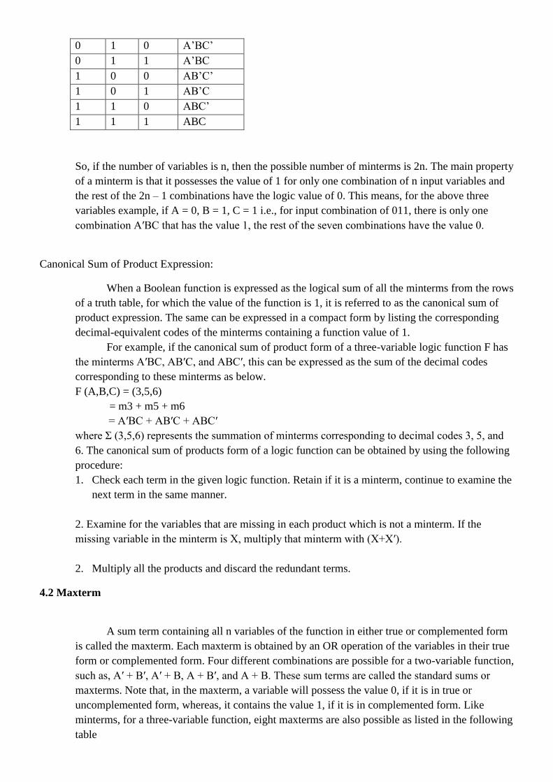
Simplification of Sum of Products Expression (SOP) Example 1: Minimize the Boolean expression Y=A’BC’D’+ A’BC’D +ABC’D’+ ABC’D +AB’C’D + A’B’CD’ on Karnaugh map

Y=A’B
’CD
’+AC’D+BC
’
Example 2:
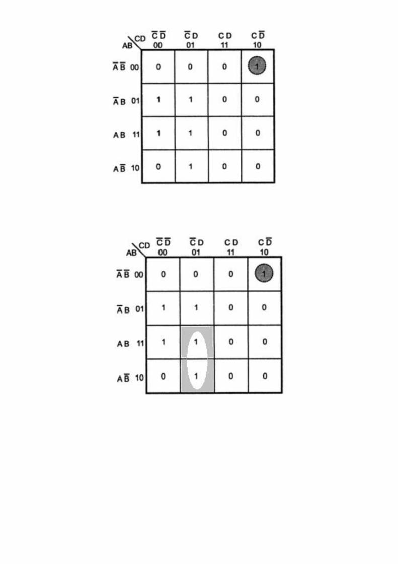
Simplify the logic function specified by the truth table using Karnaugh map method. Y is the output variable and A,B,C are the input variable
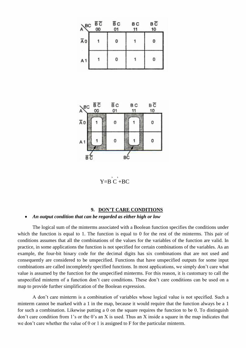
Y=B’C
’+BC
9. DON’T CARE CONDITIONS
An output condition that can be regarded as either high or low
The logical sum of the minterms associated with a Boolean function specifies the conditions under
which the function is equal to 1. The function is equal to 0 for the rest of the minterms. This pair of
conditions assumes that all the combinations of the values for the variables of the function are valid. In
practice, in some applications the function is not specified for certain combinations of the variables. As an
example, the four-bit binary code for the decimal digits has six combinations that are not used and
consequently are considered to be unspecified. Functions that have unspecified outputs for some input
combinations are called incompletely specified functions. In most applications, we simply don’t care what
value is assumed by the function for the unspecified minterms. For this reason, it is customary to call the
unspecified minterm of a function don’t care conditions. These don’t care conditions can be used on a
map to provide further simplification of the Boolean expression.
A don’t care minterm is a combination of variables whose logical value is not specified. Such a
minterm cannot be marked with a 1 in the map, because it would require that the function always be a 1
for such a combination. Likewise putting a 0 on the square requires the function to be 0. To distinguish
don’t care condition from 1’s or the 0’s an X is used. Thus an X inside a square in the map indicates that
we don’t care whether the value of 0 or 1 is assigned to F for the particular minterm.

In choosing the adjacent squares to simplify the function in a map the don’t care minterms may be
assumed to be either 0 0r 1. When simplifying the function, we can choose to include each don’t care
minterm with either the 1’s or the 0’s depending on which combination gives the simplest expression.
Example Problem:
Simplify the Boolean function F(w,x,y,z) = ∑(1,3,7,11,15) which has the don’t care conditions
d(w,x,y,z) = ∑(0,2,5).
Solution
The minterms of F are the variable combinations that make the function equal to 1. The minterms
of “d” are don’t care minterms that may be assigned either 0 or 1. The map simplification is shown in fig.
the minterms of F are marked by 1’s. Those of d are marked by X’s and remaining squares are filled with
0’s.
To get simplified expression in sum-of- product form we must include all five 1’s in the map but
we may
In the part of the diagram, don’t care minterm 0 and 2 is included the units 1’s and the simplified function
is now
F = yz+w’x’
In the second don’t care minterm 5 is included with the 1’s , and the simplified function is now
F = yz + w’z
9.1 NAND AND NOR IMPLIMENTATION

Digital circuits are frequently constructed with NAND and NOR gates rather than with AND and
OR gates. NAND and NOR gates are easier to fabricate. So rules and procedures have been developed for
the conversion from Boolean functions given in terms of AND, OR and NOT into equivalent NAND and
NOR logic diagrams.
Two level NAND- NAND implementation
To facilitate the conversion to NAND logic, it is convenient to define an alternative graphic
symbol for the gate. The alternate representation of NAND gate is shown in fig. according to De
Morgan’s theorem
Steps to be followed
1. Simplify the given logic expression and convert it in the SOP form
2. Draw the logic circuit using AND,OR and NOT gate
3. Replace every AND gate by a NAND gate, Every OR gate by a bubbled OR gate and NOT gate
by a NAND inverter.
4. Replace bubbled-OR gate by NAND gate.
Example Problem:
Implement the following Boolean equation using only NAND gatesY=AB+CDE+F
Solution
Step 1: realization using basic gates
Step 2: replace
AND →NAND
OR →bubbled – OR
NOT →NAND inverter

Step 3: draw the logic circuit using only NAND gates
9.2 Multilevel NAND circuits
The standard form of expressing Boolean function results in a two-level implementation. If has
digital system three or more levels then the most common procedure in the design of multilevel circuits is
to express the Boolean function in terms of AND, OR and compliments operations.
The general procedure for converting multilevel AND – OR logic diagram into an all NAND logic
diagram is as follows
1. Convert all AND gates to NAND gates with AND – invert graphic symbols
2. Convert all OR gates to NAND gates with invert –OR graphic symbol.
3. Check all the bubbles in the diagram. For every bubble that is not compensated by other small
circle along the same line insert an inverter or compliment the input literal.
Example Problem:
Implement the following Boolean expression using NAND gates onlyF=A(CD+B)+BC
Solution:
Step 1: Draw logic diagram using AND,OR and NOT gate as shown in the fig.

9.3 NOR IMPLEMENTATION
The NOR operation is the dual of the AND operation. Therefore all procedures and rules for NOR
logic are the dual for the corresponding procedures and rules developed for NAND logic. The NOR gate
is another universal gate that can be used to implement any Boolean function. The alternative
representation of NOR gate according to demorgan’s theorem is shown below.
Steps to be followed
1. Simply the given logic expression and convert it into product of sum (POS) form.
2. Draw the AND – OR-NOT realization.
3. Replace every OR gate by NOR, every AND gate by a bubbled AND gate and ever inerter by a
NOR inverter.
4. Draw the final circuit using only the NOR gates.
Example Problem:
Implement the following function by using NOR gates Y=(A’+B+C)(A+B)D
Solution:
Step 1: Implement the given Boolean function by usingAND, ORandNOTgate as shown below.
Step 2:
Replace OR → NOR
AND → invert AND
NOT → NOR invert

Step 3: Replace invert AND gate by NOR gate shown in fig.
9.4 MULTILEVEL NOR IMPLEMENTATION
The procedure for converting a multilevel AND-OR diagram to an all NOR diagram is similar to
multilevel NAND implements. The following steps are followed for multilevel-NOR implementation
Step 1.impliment the logic function using AND, OR and NOT gate.
Step 2.convert all AND gates to NOR gates with invert-AND graphic symbol.
Step 3.convert all OR gates with OR invert graphic symbols.
Step 4.Check all the bubbles in the diagram. For every bubble that is not compensated by another small
circle along the same line, insert an inverter or compliment the input literal.
Example Problem:
Implement the following Boolean function using NOR gatesY=(AB’+A’B)(C+D’)
Solution
Step 1: Implement the Boolean function using AND,OR and NOT gate as shown in fig.
Step 2:
Replace
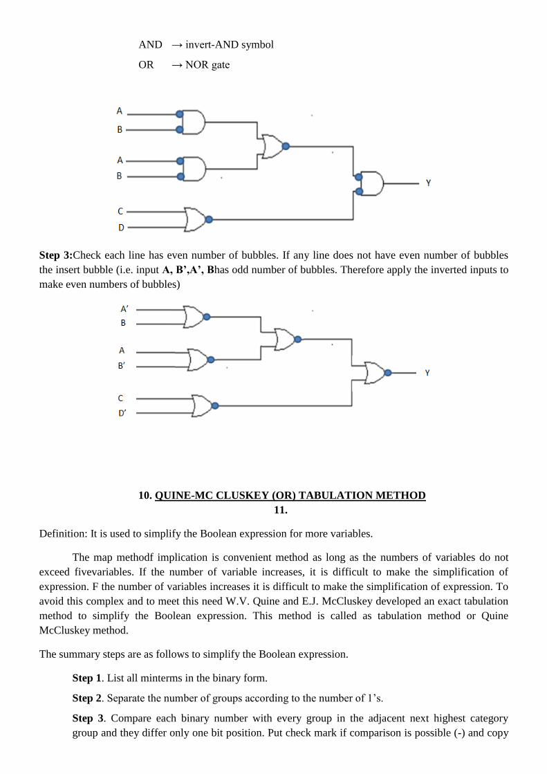
AND → invert-AND symbol
OR → NOR gate
Step 3:Check each line has even number of bubbles. If any line does not have even number of bubbles
the insert bubble (i.e. input A, B’,A’, Bhas odd number of bubbles. Therefore apply the inverted inputs to
make even numbers of bubbles)
10. QUINE-MC CLUSKEY (OR) TABULATION METHOD
11.
Definition: It is used to simplify the Boolean expression for more variables.
The map methodf implication is convenient method as long as the numbers of variables do not
exceed fivevariables. If the number of variable increases, it is difficult to make the simplification of
expression. F the number of variables increases it is difficult to make the simplification of expression. To
avoid this complex and to meet this need W.V. Quine and E.J. McCluskey developed an exact tabulation
method to simplify the Boolean expression. This method is called as tabulation method or Quine
McCluskey method.
The summary steps are as follows to simplify the Boolean expression.
Step 1. List all minterms in the binary form.
Step 2. Separate the number of groups according to the number of 1’s.
Step 3. Compare each binary number with every group in the adjacent next highest category
group and they differ only one bit position. Put check mark if comparison is possible (-) and copy

remaining term in the next column. Put (√) mark for every comparison.The essential prime
implicants are identified if they have no tick mark.
Step 4. Apply the same process described in step 3 for the resultant column and continue the
cycles until a single pass through cycle yieldsfurther elimination of literals.
Step 5. From prime implicant chart
(a) The prime implicants should be represented in rowsand each minterm of the function in a column.
(b) Crosses (X) should be placed in each row to show the composition of minterm that makes the
prime implicants.
(c) A completed prime implicants table should be inspected for columns containing only a single
cross in their columns are called essential prime implicants.
Step 6. Getting the simplified expression after the above step
Example Problem: Simplify the Boolean function by using tabulation method.
F(a,b,c,d)=∑m(0,1,2,5,6,7,8,9,10,14)
Solution
Group Column I Column II Column III
abcd abcd abcd
Group 0 0 0000√ 0,1 000√ 0,1,8,9-00-
Group 1
Number of 1’s one
1 0001√ 0,2 00-0√ 0,2,8,10-0-0
2 0010√ 0,8 -000√ 0,8,1,-00-
8 1000√ 1,5 0-01√ 0,8,2,10-0-0
Group 2
Number of 1’s two
5 0101√ 1,9 -001√ 2,6,10,14-10
6 0110√ 2,6 0-10√ 2,10,6,14-10
9 1001√ 2,10 -0-10√
10 1010√ 8,9 100√
Group 3
Number of 1’s three
7 0111√ 8,10 10-0√
14 1110√ 5,7 01-1
6,7 011-
6,14 =110√
10,14 1-10√
Table: Prime implicant table
Prime implicants minterms
0 1 2 5 6 7 8 9 10 14
1,5 d’c’d X X
5,7 a’bd X X
6,7 a’bc X X
0,1,8,9* b’c’ X X X X
0,2,8,10 b’d’ X X X X
2,10,6,14* cd’ X X X X
√ √
Note that the cells (5,7), (1,5), (6,7),(0,1,8,9),(0,2,8,10) and (2,10,6,14)are prime implicants. The
prime implicants table can be plotted as shown in table above. All the unticked terms in the above
simplification are given as prime implicant of this Boolean expression, these prime implicants chart is

shown in table. In the chart all the specified implicants form columns a cross is put in the row of each
prime implicant under the columns of the implicants which it covers.
A tick mark is placed against every essential prime implicant (which column contains a single
cross(X). the sum of essential prime implicantsF = b’c’ + cd’
The prime implicants which covers the minterms 0,1,8,9 and 2,10,6,14 therefore in order to cover
the remaining minterms, the reduced prime implicants chart is formed as follows.
To cover the minterms the prime implicants (6,7) and (0,2,8,10) can be selected in additionto the
essential prime implicants for obtaining the minimal Boolean expression is given
F = b’c’+cd’+a’bc+b’d’
Reduced prime implicant table
Prime implicants Minterms
0 1 2 5 6 7 8 9 10 14
1,5 a’c’d X X
5,7 a’bd X X
6,7 a’bc X X
0,2,8,10* b’d’ X X X X
√ √ √ √ √

SCHOOL OF ELECTRICAL AND ELECTRONICS
DEPARTMENT OF ELECTRICAL AND ELECTRONICS
UNIT –III- COMBINATIONAL LOGIC

UNIT III- COMBINATIONAL LOGIC
Design Procedure - Adder - Subtracter - Code Conversion - Analysis Procedure - Multilevel NAND/NOR
circuits - Exclusive OR functions - Binary adder and subtractor- Decimal adder - BCD adder - Magnitude
Comparator - Decoders - Demultiplexer - Encoder – Multiplexers.
Half Adder
3.1. Design Procedure - Adder - Subtracter - Code Conversion
Half adder is a combinational logic circuit with two inputs and two outputs. The half adder circuit is designed to add two
single bit binary number A and B. It is the basic building block for addition of two single bit numbers. This circuit has two
outputs carry and sum.
Block diagram Truth Table
Circuit Diagram
Full Adder
Full adder is developed to overcome the drawback of Half Adder circuit. It can add two one-bit numbers A and B, and
carry c. The full adder is a three input and two output combinational circuit.
Block diagram

Truth Table Circuit Diagram
Half Subtractors
Half subtractor is a combination circuit with two inputs and two outputs (difference and borrow). It produces the
difference between the two binary bits at the input and also produces an output (Borrow) to indicate if a 1 has been
borrowed. In the subtraction (A-B), A is called as Minuend bit and B is called as Subtrahend bit.
Truth Table Circuit Diagram
Full Subtractors
The disadvantage of a half subtractor is overcome by full subtractor. The full subtractor is a combinational circuit with
three inputs A,B,C and two output D and C'. A is the 'minuend', B is 'subtrahend', C is the 'borrow' produced by the
previous stage, D is the difference output and C' is the borrow output.
Truth Table Circuit Diagram

4 Bit Parallel Adder
In the block diagram, A0 and B0 represent the LSB of the four bit words A and B. Hence Full Adder-0 is the lowest stage.
Hence its Cin has been permanently made 0. The rest of the connections are exactly same as those of n-bit parallel adder is
shown in fig. The four bit parallel adder is a very common logic circuit.
Block diagram
Serial Adder
If speed is not of great importance, a cost-effective option is to use a serial adder
Serial adder: bits are added a pair at a time (in one clock cycle)

4 Bit Adder/ Subtractor
The circuit for subtracting A - B consists of an adder with inverters placed between each data input B and the
corresponding input of the full adder. The input carry C0 must be equal to 1 when subtraction is performed. The operation
thus performed becomes A, plus the 1’s complement of B, plus 1. This is equal to A plus the 2’s complement of B.
Code conversion


2. Analysis Procedure - Multilevel NAND/NOR circuits
Multi-Level Gate Circuits
Two-level circuits consisting of AND and OR gates can easily be converted to networks that can be realized only NAND and
NOR gates – A two-level AND-OR (SOP) circuit can be realized (directly) as a two-level NAND-NAND circuit – A two-level
OR-AND (POS) circuit can be realized (directly) as a two-level NOR-NOR circuit . The same approach can be used for
multilevel networks.
AND – OR to NAND- NAND example

OR –AND to NAND-NAND example

3. Exclusive OR functions - Binary adder and subtractor- Decimal adder - BCD
adder
Exclusive OR functions:
The XOR function operates such that when both inputs are the same the output is zero. The output is only positive
if one of the inputs is on. As a Boolean equivalency, this rule may be helpful in simplifying some Boolean
expressions. Any expression following the AB’ + A’B form (two AND gates and an OR gate) may be replaced by
a single Exclusive-OR gate.

Binary Adder (Asynchronous Ripple-Carry Adder):
A binary adder is a digital circuit that produces the arithmetic sum of two binary numbers. A binary adder can be
constructed with full adders connected in cascade with the output carry form each full adder connected to the input
carry of the next full adder in the chain. The four-bit adder is a typical example of a standard component .It can be
used in many application involving arithmetic operations.
The input carry to the adder is c0 and it ripples through the full adders to the output carry c4.
n -bit binary adder requires n full adders.

The addition of A+B binary numbers in parallel implies that all the bits of A and B are available for computation
at the same time. As in any combinational circuit, the signal must propagate through the gates before the correct
output sum is available. The output will not be correct unless the signals are given enough time to propagate
through the gates connected form the input to the output. The longest propagation delay time in an adder is the
time it takes the carry to propagate through the full adders.
The signal form the carry input Ci to the output carry Ci+1 propagates through an AND gate and an OR gate, which
equals 2 gate levels.
If there are 4 full adders in the binary adder, the output carry C4would have 2×4=8 gate levels, form C0 to C4
For an n-bit adder, 2n gate levels for the carry to propagate form input to output are required.
The carry propagation time is an important attribute of the adder because it limits the speed with which two
numbers are added.
To reduce the carry propagation delay time:
1) Employ faster gates with reduced delays.
2) Employ the principle of Carry Lookahead Logic
Proof: (using carry lookahead logic)
Pi = Ai ⊕Bi
Gi = AiBi

The output sum and carry are:
Si =Pi ⊕ Ci
Ci +1 = Gi + PiCi
Gi is known as the carry generate, and it produces a carry of 1 when both Ai and Bi are 1.
Pi called a carry propagate, it determines whether a carry into stage i will propagate into stage i+1 .
Computing the values of Pi and G
i only depend on the input operand bits (A
i & B
i) as clear from the Figure and
equations.
Thus, these signals settle to their steady-state value after the propagation through their respective gates.
Computed values of all the Pi’s are valid one XOR-gate delay after the operands A and B are made valid.
Computed values of all the Gi’s are valid one AND-gate delay after the operands A and B are made valid.
The Boolean function for the carry outputs of each stage and substitute the value of each Ci from the previous
equations:
C0= input carry
C1 = G0 + P0C0
C2 = G1 + P1C1 = G1 + P1 (G0 + P0C0) = G1 + P1G0 + P1P0C0
C3 = G2 + P2C2 = G2 + P2G1 + P2P1G0 + P2P1P0C0
Each carry signal is expressed as a direct SOP function of C0
rather than its preceding carry signal.
Since the Boolean expression for each output carry is expressed in SOP form, it can be implemented in two-level
circuits.
The 2-level implementation of the carry signals has a propagation delay of 2 gates, i.e., 2τ.
The 4-bit carry look-ahead (CLA) adder consists of 3 levels of logic:

First level: Generates all the P & G signals. Four sets of P & G logic (each consists of an XOR gate and an AND gate).
Output signals of this level (P’s & G’s) will be valid after 1τ.
Second level: The Carry Look-Ahead (CLA) logic block which consists of four 2-level implementation logic circuits.
It generates the carry signals (C0, C
1, C
2, and C
3) as defined by the above expressions. Output signals of this level (C
0,
C1, C
2, and C
3) will be valid after 3τ.
Third level: Four XOR gates which generate the sum signals (Si) (S
i = P
i ⊕ C
i). Output signals of this level (S
0, S
1, S
2,
and S3) will be valid after 4τ.
Thus, the 4 Sum signals (S0, S
1, S
2 & S
3) will all be valid after a total delay of 4τ compared to a delay of (2n+1)τ for
Ripple Carry adders.
For a 4-bit adder (n = 4), the Ripple Carry adder delay is 9τ.
The disadvantage of the CLA adders is that the carry expressions (and hence logic) become quite complex for more
than 4 bits.
Thus, CLA adders are usually implemented as 4-bit modules that are used to build larger size adders.
Binary Subtractor
To perform the subtraction, we can use the 2's complements, so the subtraction can be converted to addition.
2's complement can be obtained by talking the 1’s complement and adding 1 to the LSD bit.
1) 1’s complement can be implemented with inverters.
2) 1 can be added to the sum through the input carry.
The circuit for subtracting A-B consists of an adder with inverters placed between each data input B and the
corresponding input of the full adder. The input carry C0 must be equal to 1.
Binary Parallel Adder/Subtractor: The addition and subtraction operations can be done using an Adder-Subtractor circuit. The figure shows the logic
diagram of a 4-bit Adder-Subtractor circuit.

The circuit has a mode control signal M which determines if the circuit is to operate as an adder or a subtractor. Each XOR gate receives input M and one of the inputs of B, i.e., B
i. To understand the behavior of XOR gate consider
its truth table given below.
If one input of XOR gate is zero then the output of XOR will be same as the second input. While if one input of XOR
gate is one then the output of XOR will be complement of the second input.
So when M = 0, the output of XOR gate will be Bi ⊕ 0 = B
i. If the full adders receive the value of B, and the input
carry C0
is 0, the circuit performs A plus B.
When M = 1, the output of XOR gate will be Bi ⊕ 1 = B
i
’
. If the full adders receive the value of B’, and the input carry
C0 is 1, the circuit performs A plus 1’s complement of B plus 1, which is equal to A minus B.
BCD ADDER:
Computers or calculators that perform arithmetic operations directly in the decimal number system represent
decimal numbers in binary coded form.
An adder for such a computer must employ arithmetic circuits that accept coded decimal numbers and present
results in the same code. For binary addition, it is sufficient to consider a pair of significant bits together with a

previous carry. A decimal adder requires a minimum of nine inputs and five outputs, since four bits are required to
code each decimal digit and the circuit must have an input and output carry
(1 digit requires 4-bit
Input: 2 digits + 1-bit carry
Output: 1 digit + 1-bit carry)
Since each input digit does not exceed 9, the output sum cannot be greater than 9 + 9 + 1 = 19, the 1 in the sum
being an input carry.
Suppose we apply two BCD digits to a four-bit binary adder. The adder will form the sum in binary and produce a
result that ranges from 0 through 19.
These binary numbers are labeled by symbols K, Z8, Z4, Z2, and Z1. K is the carry, and the subscripts under the
letter Z represent the weights 8, 4, 2, and 1 that can be assigned to the four bits in the BCD code.
When the binary sum is equal to or less than 1001b
BCD Sum = Binary Sum
C = 0 ;
When the binary sum is greater than 1001b
BCD Sum = Binary Sum + 0110b
C = 1
The condition for a correction and an output carry can be expressed by the Boolean function
C = K + Z8.Z4 + Z8.Z2
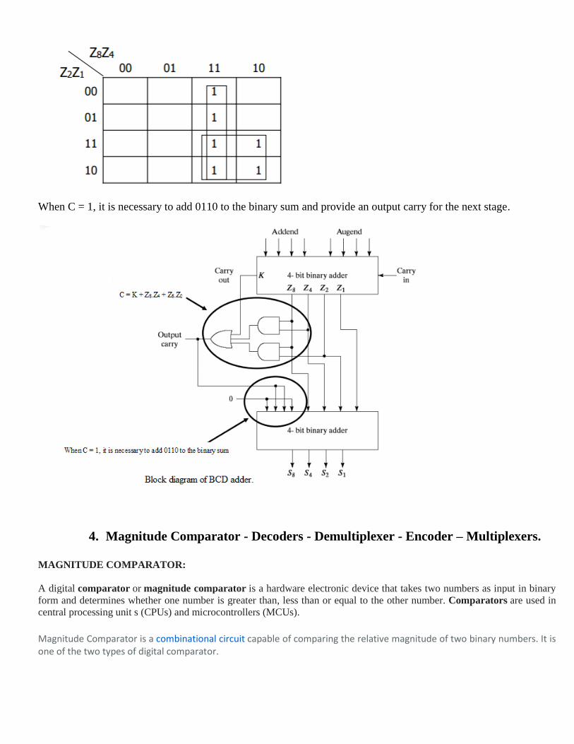
When C = 1, it is necessary to add 0110 to the binary sum and provide an output carry for the next stage.
4. Magnitude Comparator - Decoders - Demultiplexer - Encoder – Multiplexers.
MAGNITUDE COMPARATOR:
A digital comparator or magnitude comparator is a hardware electronic device that takes two numbers as input in binary
form and determines whether one number is greater than, less than or equal to the other number. Comparators are used in
central processing unit s (CPUs) and microcontrollers (MCUs).
Magnitude Comparator is a combinational circuit capable of comparing the relative magnitude of two binary numbers. It is one of the two types of digital comparator.
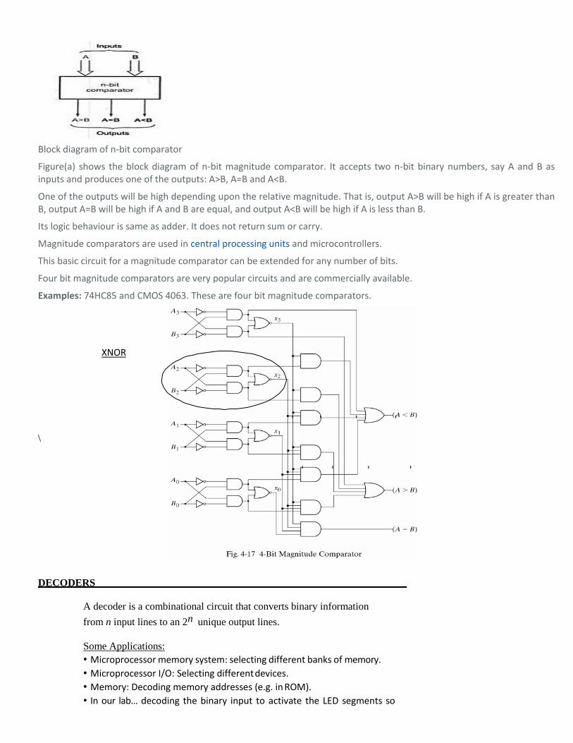
Block diagram of n-bit comparator
Figure(a) shows the block diagram of n-bit magnitude comparator. It accepts two n-bit binary numbers, say A and B as inputs and produces one of the outputs: A>B, A=B and A<B.
One of the outputs will be high depending upon the relative magnitude. That is, output A>B will be high if A is greater than B, output A=B will be high if A and B are equal, and output A<B will be high if A is less than B.
Its logic behaviour is same as adder. It does not return sum or carry.
Magnitude comparators are used in central processing units and microcontrollers.
This basic circuit for a magnitude comparator can be extended for any number of bits.
Four bit magnitude comparators are very popular circuits and are commercially available.
Examples: 74HC85 and CMOS 4063. These are four bit magnitude comparators.
XNOR
' ' ' '
\
' ' ' '
DECODERS
A decoder is a combinational circuit that converts binary information
from n input lines to an 2n unique output lines.
Some Applications:
• Microprocessor memory system: selecting different banks of memory.
• Microprocessor I/O: Selecting different devices.
• Memory: Decoding memory addresses (e.g. in ROM).
• In our lab… decoding the binary input to activate the LED segments so

that the decimal number can be displayed.

3-to-8-line DECODER
Binary Inputs
Outputs
D0 D1 D2 D3 D4 D5 D6 D7
0 0 0 1 0 0 0 0 0 0 0
0 0 1 0 1 0 0 0 0 0 0
0 1 0 0 0 1 0 0 0 0 0
0 1 1 0 0 0 1 0 0 0 0
1 0 0 0 0 0 0 1 0 0 0
1 0 1 0 0 0 0 0 1 0 0
1 1 0 0 0 0 0 0 0 1 0
1 1 1 0 0 0 0 0 0 0 1
If the input corresponds to minterm mi then the decoder ouputi
will be the single asserted output.
3-to-8-line DECODER

3-to-8-line DECODER

2-to-4-line DECODER with Enable
The decoder is enabled when E = 0. The output whose value = 0
represents the minterm is selected by inputs A and B.
The decoder is inactive when E = 1€ D0 … D3 = 1
A Decoder with enable input is called a decoder/ demultiplexer.
Demultiplexer receives information from a single line and directs it
to the output lines.
Complemented outputs
A 4 x 16 DECODER
• When w = 0, the top decoder is enabled and the bottom
is disabled. Top decoder generates 8 minterms 0000 to
0111, while the bottom decoder outputs are 0’s.
• When w = 1, the top decoder is disabled and the bottom
is enabled. Bottom decoder generates 8 minterms 1000 to
1111, while the top decoder outputs are 0’s.
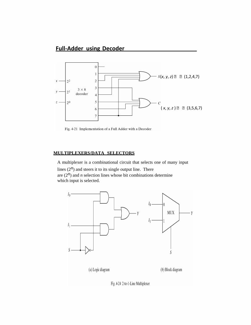
Full-Adder using Decoder
(x, y, z) (1,2,4,7)
( x, y, z ) (3,5,6,7)
MULTIPLEXERS/DATA SELECTORS
A multiplexer is a combinational circuit that selects one of many input
lines (2n) and steers it to its single output line. There
are (2n) and n selection lines whose bit combinations determine
which input is selected.

4-to-1LINE MULTIPLEXER DESIGN
In general, a 2n–to–1- line multiplexer is constructed from an
n–to 2n decoder by adding to it 2n lines, one to each AND gate.
1
0

QUADRUPLE 4-to-1LINE MULTIPLEXER
Function implementation using multiplexers
Function with n variables and multiplexer with n – 1 selection
F (x, y, z) (1,2,6,7)
Input variables x, y: Selection lines, S1 and S0
Variable z: Date line 0
Data lines 1,2,3: z', 0,1
OR gates
are
included

Function implementation using 4x1multiplexer
’
Function implementation using 8x1multiplexer
F ( A, B,C, D) (1,3,4,11,12,13,14,15)
1. Complete the truth table from the SOP.
2. The first n – 1 variables in the table are applied to the
selection inputs of the multiplexer.
3. For each combination of the selection variables, we evaluate the
output as a function of the last variable.
4. Apply these values to the data input in proper order.

Function implementation using 8x1 MUX
note the order of input
lines
Three State Gates
A three-state gate is a digital circuit that exhibits three states: 0, 1 and a
high- impedance (high z state). The high impedance state behaves as an
open circuit.
Because of this feature (high z state), a large number of three-state gate
outputs can be connected to form a common line without endangering
load effects.

Function implementation using 8x1 MUX
The data distributor, known more commonly as a Demultiplexer or “Demux” for short, is the exact opposite of
the Multiplexer
The demultiplexer takes one single input data line and then switches it to any one of a number of individual output lines
one at a time. The demultiplexer converts a serial data signal at the input to a parallel data at its output lines as shown
below.
1-to-4 Channel De-multiplexer
Output Select
Data Output
Selected
b a
0 0 A
0 1 B

Function implementation using 8x1 MUX
1 0 C
1 1 D
The Boolean expression for this 1-to-4 Demultiplexer above with outputs A to D and data select lines a, b is given as:
F = abA + abB + abC + abD
The function of the Demultiplexer is to switch one common data input line to any one of the 4 output data
lines A to D in our example above. As with the multiplexer the individual solid state switches are selected by the binary
input address code on the output select pins “a” and “b” as shown.
Demultiplexer Output Line Selection
As with the previous multiplexer circuit, adding more address line inputs it is possible to switch more outputs giving a
1-to-2n data line outputs.
Some standard demultiplexer IC´s also have an additional “enable output” pin which disables or prevents the input from
being passed to the selected output. Also some have latches built into their outputs to maintain the output logic level
after the address inputs have been changed. However, in standard decoder type circuits the address input will determine
which single data output will have the same value as the data input with all other data outputs having the value of logic
“0”.
The implementation of the Boolean expression above using individual logic gates would require the use of six
individual gates consisting of AND and NOT gates as shown.

Function implementation using 8x1 MUX
4 Channel Demultiplexer using Logic Gates
The symbol used in logic diagrams to identify a demultiplexer is as follows.
The Demultiplexer Symbol
Again, as with the previous multiplexer example, we can also use the demultiplexer to digitally control the gain of an
operational amplifier as shown.
Applications of Demultiplexer:
1. Demultiplexer is used to connect a single source to multiple destinations. The main application area of
demultiplexer is communication system where multiplexer are used. Most of the communication system are
bidirectional i.e. they function in both ways (transmitting and receiving signals). Hence, for most of the
applications, the multiplexer and demultiplexer work in sync. Demultiplexer are also used for reconstruction of
parallel data and ALU circuits.
2. Communication System – Communication system use multiplexer to carry multiple data like audio, video and
other form of data using a single line for transmission. This process make the transmission easier. The
demultiplexer receive the output signals of the multiplexer and converts them back to the original form of the

Function implementation using 8x1 MUX
data at the receiving end. The multiplexer and demultiplexer work together to carry out the process of
transmission and reception of data in communication system.
3. ALU (Arithmetic Logic Unit) – In an ALU circuit, the output of ALU can be stored in multiple registers or storage
units with the help of demultiplexer. The output of ALU is fed as the data input to the demultiplexer. Each output
of demultiplexer is connected to multiple register which can be stored in the registers.
4. Serial to parallel converter – A serial to parallel converter is used for reconstructing parallel data from incoming
serial data stream. In this technique, serial data from the incoming serial data stream is given as data input to
the demultiplexer at the regular intervals. A counter is attach to the control input of the demultiplexer. This
counter directs the data signal to the output of the demultiplexer where these data signals are stored. When all
data signals have been stored, the output of the demultiplexer can be retrieved and read out in parallel.
Encoder
An encoder is a circuit that changes a set of signals into a code. Let’s
begin making a 2-to-1 line encoder truth table by reversing the 1-to-2 decoder
truth table.
This truth table is a little short. A complete truth table would be
One question we need to answer is what to do with those other inputs? Do
we ignore them? Do we have them generate an additional error output? In many
circuits this problem is solved by adding sequential logic in order to know not
just what input is active but also which order the inputs became active.
A more useful application of combinational encoder design is a binary to
7-segment encoder. The seven segments are given according

Function implementation using 8x1 MUX
Our truth table is:
Deciding what to do with the remaining six entries of the truth table is
easier with this circuit. This circuit should not be expected to encode an
undefined combination of inputs, so we can leave them as “don’t care” when we
design the circuit. The equations were simplified with karnaugh maps.

Function implementation using 8x1 MUX
The collection of equations is summarised here:

Function implementation using 8x1 MUX
The circuit is:

Function implementation using 8x1 MUX
Reference
1. http://www.tutorialspoint.com/computer_logical_organization/combinational_circuits.htm
2. “Digital Logic and Computer design” by M. Morris Mano 3. Textbook of Digital Fundamentals by Thomas L. Floyd (9th Edition)
4. Logic and Computer Design Fundamentals (4th Edition) 4th Edition by M. Morris R.
5. Mano , Charles R. Kime.
6. www.electronicsinourhands.blogspot.com/2012/10/bcd-adder.html
7. www.electronics-tutorials.ws › Combinational Logic

SCHOOL OF ELECTRICAL AND ELECTRONICS
DEPARTMENT OF ELECTRICAL AND ELECTRONICS
UNIT –IV- SYNCHRONOUS SEQUENTIAL LOGIC
UNIT IV- SYNCHRONOUS SEQUENTIAL LOGIC
Flip Flops - Analysis of clocked sequential circuit -Flip flop excitation tables - Design Procedure - Design
of counters - Registers - Shift registers - Synchronous Counters - Timing sequences- Algorithmic State
Machines - ASM chart - timing considerations - control implementation
4.1. FLIP-FLOP
In electronics, a flip-flop or latch is a circuit that has two stable states and
can be used to store state information. Flip-flops and latches are used as data
storage elements. A flip-flop stores a single bit (binary digit) of data; one of its two
states represents a "one" and the other represents a "zero". Such data storage can be
used for storage of state, and such a circuit is described as sequential logic. When
used in a finite-state machine, the output and next state depend not only on its
current input, but also on its current state (and hence, previous inputs). It can also
be used for counting of pulses, and for synchronizing variably-timed input signals
to some reference timing signal.
Flip-flops can be either simple (transparent or opaque) or clocked (synchronous or
edge-triggered). Although the term flip-flop has historically referred generically to
both simple and clocked circuits, in modern usage it is common to reserve the term
flip-flop exclusively for discussing clocked circuits; the simple ones are commonly
called latches.
Using this terminology, a latch is level-sensitive, whereas a flip-flop is edge-
sensitive. That is, when a latch is enabled it becomes transparent, while a flip flop's
output only changes on a single type (positive going or negative going) of clock
edge.
4.2 Flip-flop types
Flip-flops can be divided into common types
1. SR ("set-reset")
2. D ("data" or "delay"[12])

3. T ("toggle")
4. JK types are the common ones.
2. Analysis of clocked sequential circuit
Sequential Logic Circuits
Unlike Combinational Logic circuits that change state depending upon the actual
signals being applied to their inputs at that time, Sequential Logic circuits have
some form of inherent “Memory” built in to them as they are able to take into
account their previous input state as well as those actually present, a sort
of “before” and “after” effect is involved with sequential logic circuits.
In other words, the output state of a “sequential logic circuit” is a function of
the following three states, the “present input”, the “past input” and/or the “past
output”. Sequential Logic circuits remember these conditions and stay fixed in
their current state until the next clock signal changes one of the states, giving
sequential logic circuits “Memory”.
Sequential logic circuits are generally termed as two state or Bistable
devices which can have their output or outputs set in one of two basic states, a
logic level “1” or a logic level “0” and will remain “latched” (hence the name
latch) indefinitely in this current state or condition until some other input trigger
pulse or signal is applied which will cause the bistable to change its state once
again.
The word “Sequential” means that things happen in a “sequence”, one after
another and in Sequential Logic circuits, the actual clock signal determines when

things will happen next. Simple sequential logic circuits can be constructed from
standard Bistable circuits such as: Flip-flops, Latches and Counters and which
themselves can be made by simply connecting together universal NAND Gates
and/or NOR Gates in a particular combinational way to produce the required
sequential circuit
3. Flip flop excitation tables - Flip flop excitation tables
- Design Procedure of SR, Jk, D T flipflops
SR Flip-Flop
The SR flip-flop, also known as a SR Latch, can be considered as one of the
most basic sequential logic circuit possible. This simple flip-flop is basically a one-
bit memory bistable device that has two inputs, one which will “SET” the device
(meaning the output = “1”), and is labelled S and another which will “RESET” the
device (meaning the output = “0”), labelled R.
Then the SR description stands for “Set-Reset”. The reset input resets the
flip-flop back to its original state with an output Q that will be either at a logic
level “1” or logic “0” depending upon this set/reset condition.
A basic NAND gate SR flip-flop circuit provides feedback from both of its
outputs back to its opposing inputs and is commonly used in memory circuits to
store a single data bit. Then the SR flip-flop actually has three inputs, Set, Reset
and its current output Q relating to it’s current state or history. The term “Flip-
flop” relates to the actual operation of the device, as it can be “flipped” into one
logic Set state or “flopped” back into the opposing logic Reset state.
The Basic SR Flip-flop

The Set State
Consider the circuit shown above. If the input R is at logic level “0” (R = 0)
and input S is at logic level “1” (S = 1), the NAND gate Y has at least one of its
inputs at logic “0” therefore, its output Q must be at a logic level “1” (NAND Gate
principles). Output Q is also fed back to input “A” and so both inputs to NAND
gate X are at logic level “1”, and therefore its output Q must be at logic level “0”.
Again NAND gate principals. If the reset input R changes state, and goes
HIGH to logic “1” with S remaining HIGH also at logic level “1”, NAND gate Y
inputs are now R = “1” and B = “0”. Since one of its inputs is still at logic level “0”
the output at Q still remains HIGH at logic level “1” and there is no change of
state. Therefore, the flip-flop circuit is said to be “Latched” or “Set” with Q = “1”
and Q = “0”.
Reset State
In this second stable state, Q is at logic level “0”, (not Q = “0”) its inverse
output at Q is at logic level “1”, (Q = “1”), and is given by R = “1” and S = “0”. As
gate X has one of its inputs at logic “0” its output Q must equal logic level “1”
(again NAND gate principles). Output Q is fed back to input “B”, so both inputs to
NAND gate Y are at logic “1”, therefore, Q = “0”.
If the set input, S now changes state to logic “1” with input R remaining at
logic “1”, output Q still remains LOW at logic level “0” and there is no change of
state. Therefore, the flip-flop circuits “Reset” state has also been latched and we
can define this “set/reset” action in the following truth table.
Truth Table for this Set-Reset Function

It can be seen that when both inputs S = “1” and R = “1” the outputs Q and
Q can be at either logic level “1” or “0”, depending upon the state of the inputs S
or R BEFORE this input condition existed. Therefore the condition of S = R = “1”
does not change the state of the outputs Q and Q.
However, the input state of S = “0” and R = “0” is an undesirable or invalid
condition and must be avoided. The condition of S = R = “0” causes both outputs
Q and Q to be HIGH together at logic level “1” when we would normally want Q
to be the inverse of Q. The result is that the flip-flop looses control of Q and Q, and
if the two inputs are now switched “HIGH” again after this condition to logic “1”,
the flip-flop becomes unstable and switches to an unknown data state based upon
the unbalance as shown in the following switching diagram.
S-R Flip-flop Switching Diagram
This unbalance can cause one of the outputs to switch faster than the other
resulting in the flip-flop switching to one state or the other which may not be the
required state and data corruption will exist. This unstable condition is generally
known as its Meta-stable state.
Then, a simple NAND gate SR flip-flop or NAND gate SR latch can be set
by applying a logic “0”, (LOW) condition to its Set input and reset again by then
applying a logic “0” to its Reset input. The SR flip-flop is said to be in an “invalid”
condition (Meta-stable) if both the set and reset inputs are activated
simultaneously.

Latch Flip Flop
The R-S (Reset Set) flip flop is the simplest flip flop of all and easiest to
understand. It is basically a device which has two outputs one output being the
inverse or complement of the other, and two inputs. A pulse on one of the inputs to
take on a particular logical state. The outputs will then remain in this state until a
similar pulse is applied to the other input. The two inputs are called the Set and
Reset input (sometimes called the preset and clear inputs).
Such flip flop can be made simply by cross coupling two inverting gates
either NAND or NOR gate could be used Figure 1(a) shows on RS flip flop using
NAND gate and Figure 1(b) sh ows the same circuit using NOR gate.
Figure 1: Latch R-S Flip Flop Using NAND and NOR Gates
To describe the circuit of Figure 1(a), assume that initially both R and S are
at the logic 1 state and that output is at the logic 0 state.
Now, if Q = 0 and R = 1, then these are the states of inputs of gate B,
therefore the outputs of gate B is at 1 (making it the inverse of Q i.e. 0). The output
of gate B is connected to an input of gate A so if S = 1, both inputs of gate A are at
the logic 1 state. This means that the output of gate A must be 0 (as was originally
specified). In other words, the 0 state at Q is continuously disabling gate B so that

any change in R has no effect. Also the 1 state at is continuously enabling gate A
so that any change S will be transmitted through to Q. The above conditions
constitute one of the stable states of the device referred to as the Reset state since
Q = 0.
Now suppose that the R-S flip flop in the Reset state, the S input goes to 0.
The output of gate A i.e. Q will go to 1 and with Q = 1 and R = 1, the output of
gates B ( ) will go to 0 with now 0 gate A is disabled keeping Q at 1.
Consequently, when S returns to the 1 state it has no effect on the flip flop whereas
a change in R will cause a change in the output of gate B. The above conditions
constitute the other stable state of the device, called the Set state since Q = 1. Note
that the change of the state of S from 1 to 0 has caused the flip flop to change from
the Reset state to the Set state.
There is another input condition which has not yet been considered. That is
when both the R and S inputs are taken to the logic state 0. When this happens both
Q and will be forced to 1 and will remain so far as long as R and S are kept at 0.
However when both inputs return to 1 there is no way of knowing whether the flip
flop will latch in the Reset state or the Set state. The condition is said to be
indeterminate because of this indeterminate state great care must be taken when
using R-S flip flop to ensure that both inputs are not instructed simultaneously.
Table 1: The truth table for the NAND R-S flip flop
Table 2: Simple NAND R-S Flip Flop Truth Table

Table 3: NOR Gate R-S Flip Flop Truth Table
Clocked RS Flip Flop
The RS latch flip flop required the direct input but no clock. It is very use
full to add clock to control precisely the time at which the flip flop changes the
state of its output.
In the clocked R-S flip flop the appropriate levels applied to their inputs are
blocked till the receipt of a pulse from an other source called clock. The flip flop
changes state only when clock pulse is applied depending upon the inputs. The
basic circuit is shown in Figure 2. This circuit is formed by adding two AND gates
at inputs to the R-S flip flop. In addition to control inputs Set (S) and Reset (R),
there is a clock input (C) also.
Figure 2: Clocked RS Flip Flop

Table 4: The truth table for the Clocked R-S flip flop
Table 5: Excitation table for R-S Flip Flop
D Flip Flop
A D type (Data or delay flip flop) has a single data input in addition to the
clock input as shown in Figure 3.
Figure 3: D Flip Flop

Basically, such type of flip flop is a modification of clocked RS flip flop
gates from a basic Latch flip flop and NOR gates modify it in to a clock RS flip
flop. The D input goes directly to S input and its complement through NOT gate, is
applied to the R input.
This kind of flip flop prevents the value of D from reaching the output until
a clock pulse occurs. The action of circuit is straight forward as follows.
When the clock is low, both AND gates are disabled, there fore D can
change values with out affecting the value of Q. On the other hand, when the clock
is high, both AND gates are enabled. In this case, Q is forced equal to D when the
clock again goes low, Q retains or stores the last value of D. The truth table for
such a flip flop is as given below in table 6.
Table 6: Truth table for D Flip Flop
Table 7: Excitation table for D Flip Flop
JK Flip Flop
One of the most useful and versatile flip flop is the JK flip flop the unique features
of a JK flip flop are:
1. If the J and K input are both at 1 and the clock pulse is applied, then the
output will change state, regardless of its previous condition.
2. If both J and K inputs are at 0 and the clock pulse is applied there will be no
change in the output. There is no indeterminate condition, in the operation of
JK flip flop i.e. it has no ambiguous state. The circuit diagram for a JK flip
flop is shown in Figure 4.

Figure 4: JK Flip Flop
When J = 0 and K = 0
These J and K inputs disable the NAND gates, therefore clock pulse have no effect
on the flip flop. In other words, Q returns it last value.
When J = 0 and K = 1,
The upper NAND gate is disabled the lower NAND gate is enabled if Q is 1
therefore, flip flop will be reset (Q = 0 , =1)if not already in that state.
When J = 1 and K = 0
The lower NAND gate is disabled and the upper NAND gate is enabled if is at 1,
As a result we will be able to set the flip flop ( Q = 1, = 0) if not already set
When J = 1 and K = 1
If Q = 0 the lower NAND gate is disabled the upper NAND gate is enabled. This
will set the flip flop and hence Q will be 1. On the other hand if Q = 1, the lower
NAND gate is enabled and flip flop will be reset and hence Q will be 0. In other
words , when J and K are both high, the clock pulses cause the JK flip flop to
toggle. Truth table for JK flip flop is shown in table 8.
Table 8: The truth table for the JK flip flop

Table 6: Excitation table for JK Flip Flop
T Flip Flop
A method of avoiding the indeterminate state found in the working of RS
flip flop is to provide only one input ( the T input ) such, flip flop acts as a toggle
switch. Toggle means to change in the previous stage i.e. switch to opposite state.
It can be constructed from clocked RS flip flop be incorporating feedback from
output to input as shown in Figure 5.
Figure 5: T Flip Flop
Such a flip flop is also called toggle flip flop. In such a flip flop a train of
extremely narrow triggers drives the T input each time one of these triggers, the
output of the flip flop changes stage. For instance Q equals 0 just before the
trigger. Then the upper AND gate is enable and the lower AND gate is disabled.
When the trigger arrives, it results in a high S input.
This sets the Q output to 1. When the next trigger appears at the point T, the
lower AND gate is enabled and the trigger passes through to the R input this forces
the flip flop to reset.
Since each incoming trigger is alternately changed into the set and reset
inputs the flip flop toggles. It takes two triggers to produce one cycle of the output
waveform. This means the output has half the frequency of the input stated another
way, a T flip flop divides the input frequency by two. Thus such a circuit is also
called a divide by two circuit.

A disadvantage of the toggle flip flop is that the state of the flip flop after a
trigger pulse has been applied is only known if the previous state is known. The
truth table for a T flip flop is as given table 7.
Table 7: Truth table for T Flip Flop
Table 8: Excitation table for T Flip Flop
Generally T flip flop ICs are not available. It can be constructed using JK, RS or D
flip flop. Figure 6 shows the relation of T flip flop using JK flip flop.
A D-type flip flop may be modified by external connection as a T-type stage
as shown in Figure 7. Since the Q logic is used as D-input the opposite of the Q

output is transferred into the stage each clock pulse. Thus the stage having Q - 0
transistors = 1, Providing a toggle action, if the stage had Q = 1 the clock pulse
would result in Q = 0 being transferred, again providing the toggle operation. The
D-type flip flop connected as in Figure 6 will thus operate as a T-type stage,
complementing each clock pulse.
Master Slave Flip Flop
Figure 8 shows the schematic diagram of master sloave J-K flip flop
Figure 8: Master Slave JK Flip Flop
A master slave flip flop contains two clocked flip flops. The first is called
master and the second slave. When the clock is high the master is active. The
output of the master is set or reset according to the state of the input. As the slave
is inactive during this period its output remains in the previous state. When clock
becomes low the output of the slave flip flop changes because it become active
during low clock period. The final output of master slave flip flop is the output of
the slave flip flop. So the output of master slave flip flop is available at the end of a
clock pulse.
4. Design of counters
Counter is a sequential circuit. A digital circuit which is used for a counting pulses
is known counter. Counter is the widest application of flip-flops. It is a group of
flip-flops with a clock signal applied. Counters are of two types.
Asynchronous or ripple counters.
Synchronous counters
5. Registers
Flip-flop is a 1 bit memory cell which can be used for storing the digital
data. To increase the storage capacity in terms of number of bits, we have to use a
group of flip-flop. Such a group of flip-flop is known as a Register. The n-bit

register will consist of n number of flip-flop and it is capable of storing an n-bit
word.
6. Shift Register
The Shift Register is another type of sequential logic circuit that can be used
for the storage or the transfer of data in the form of binary numbers. This
sequential device loads the data present on its inputs and then moves or “shifts” it
to its output once every clock cycle, hence the name “shift register”.
A shift register basically consists of several single bit “D-Type Data Latches”, one
for each data bit, either a logic “0” or a “1”, connected together in a serial type
daisy-chain arrangement so that the output from one data latch becomes the input
of the next latch and so on.
Data bits may be fed in or out of a shift register serially, that is one after the other
from either the left or the right direction, or all together at the same time in a
parallel configuration.
The number of individual data latches required to make up a single Shift
Register device is usually determined by the number of bits to be stored with the
most common being 8-bits (one byte) wide constructed from eight individual data
latches.
Shift Registers are used for data storage or for the movement of data and are
therefore commonly used inside calculators or computers to store data such as two
binary numbers before they are added together, or to convert the data from either a
serial to parallel or parallel to serial format. The individual data latches that make
up a single shift register are all driven by a common clock ( Clk ) signal making
them synchronous devices.
Shift register IC’s are generally provided with a clear or reset connection so that
they can be “SET” or “RESET” as required. Generally, shift registers operate in
one of four different modes with the basic movement of data through a shift
register being:
Serial-in to Parallel-out (SIPO) - the register is loaded with serial data, one bit
at a time, with the stored data being available at the output in parallel form.

Serial-in to Serial-out (SISO) - the data is shifted serially “IN” and “OUT” of
the register, one bit at a time in either a left or right direction under clock control.
Parallel-in to Serial-out (PISO) - the parallel data is loaded into the register
simultaneously and is shifted out of the register serially one bit at a time under
clock control.
Parallel-in to Parallel-out (PIPO) - the parallel data is loaded simultaneously
into the register, and transferred together to their respective outputs by the same
clock pulse.
The effect of data movement from left to right through a shift register can be
presented graphically as:
Also, the directional movement of the data through a shift register can be either to
the left, (left shifting) to the right, (right shifting) left-in but right-out, (rotation) or
both left and right shifting within the same register thereby making it bidirectional.
In this tutorial it is assumed that all the data shifts to the right, (right shifting).
4-bit Serial-in to Parallel-out Shift Register

The operation is as follows. Lets assume that all the flip-flops ( FFA to FFD ) have
just been RESET ( CLEAR input ) and that all the outputs QA to QD are at logic
level “0” ie, no parallel data output.
If a logic “1” is connected to the DATA input pin of FFA then on the first clock
pulse the output of FFA and therefore the resulting QA will be set HIGH to logic
“1” with all the other outputs still remaining LOW at logic “0”. Assume now that
the DATA input pin of FFA has returned LOW again to logic “0” giving us one
data pulse or 0-1-0.
The second clock pulse will change the output of FFA to logic “0” and the output
of FFB and QB HIGH to logic “1” as its input D has the logic “1” level on it
from QA. The logic “1” has now moved or been “shifted” one place along the
register to the right as it is now atQA.
When the third clock pulse arrives this logic “1” value moves to the output
of FFC ( QC ) and so on until the arrival of the fifth clock pulse which sets all the
outputs QA to QD back again to logic level “0” because the input to FFA has
remained constant at logic level “0”.
The effect of each clock pulse is to shift the data contents of each stage one place
to the right, and this is shown in the following table until the complete data value
of 0-0-0-1 is stored in the register. This data value can now be read directly from
the outputs of QA to QD.

Then the data has been converted from a serial data input signal to a parallel data
output. The truth table and following waveforms show the propagation of the logic
“1” through the register from left to right as follows.
Basic Data Movement Through A Shift Register
Clock
Pulse
No
QA QB QC QD
0 0 0 0 0
1 1 0 0 0
2 0 1 0 0
3 0 0 1 0
4 0 0 0 1
5 0 0 0 0

Note that after the fourth clock pulse has ended the 4-bits of data ( 0-0-0-1 ) are
stored in the register and will remain there provided clocking of the register has
stopped. In practice the input data to the register may consist of various
combinations of logic “1” and “0”. Commonly available SIPO IC’s include the
standard 8-bit 74LS164 or the 74LS594.
Serial-in to Serial-out (SISO) Shift Register
This shift register is very similar to the SIPO above, except were before the
data was read directly in a parallel form from the outputs QA to QD, this time the
data is allowed to flow straight through the register and out of the other end. Since
there is only one output, the DATA leaves the shift register one bit at a time in a
serial pattern, hence the name Serial-in to Serial-Out Shift Register or SISO.
The SISO shift register is one of the simplest of the four configurations as it
has only three connections, the serial input (SI) which determines what enters the
left hand flip-flop, the serial output (SO) which is taken from the output of the
right hand flip-flop and the sequencing clock signal (Clk). The logic circuit
diagram below shows a generalized serial-in serial-out shift register.

4-bit Serial-in to Serial-out Shift Register
You may think what the point of a SISO shift register is if the output data is
exactly the same as the input data. Well this type of Shift Register also acts as a
temporary storage device or it can act as a time delay device for the data, with the
amount of time delay being controlled by the number of stages in the register, 4, 8,
16 etc or by varying the application of the clock pulses. Commonly available IC’s
include the 74HC595 8-bit Serial-in to Serial-out Shift Register all with 3-state
outputs.
Parallel-in to Serial-out (PISO) Shift Register
The Parallel-in to Serial-out shift register acts in the opposite way to the
serial-in to parallel-out one above. The data is loaded into the register in a parallel
format in which all the data bits enter their inputs simultaneously, to the parallel
input pins PA to PD of the register. The data is then read out sequentially in the
normal shift-right mode from the register at Q representing the data present
at PA to PD.
This data is outputted one bit at a time on each clock cycle in a serial format.
It is important to note that with this type of data register a clock pulse is not
required to parallel load the register as it is already present, but four clock pulses
are required to unload the data.

4-bit Parallel-in to Serial-out Shift Register
As this type of shift register converts parallel data, such as an 8-bit data
word into serial format, it can be used to multiplex many different input lines into a
single serial DATA stream which can be sent directly to a computer or transmitted
over a communications line. Commonly available IC’s include the 74HC166 8-bit
Parallel-in/Serial-out Shift Registers.
Parallel-in to Parallel-out (PIPO) Shift Register
The final mode of operation is the Parallel-in to Parallel-out Shift Register.
This type of shift register also acts as a temporary storage device or as a time delay
device similar to the SISO configuration above. The data is presented in a parallel
format to the parallel input pins PA to PD and then transferred together directly to
their respective output pins QA to QA by the same clock pulse. Then one clock
pulse loads and unloads the register. This arrangement for parallel loading and
unloading is shown below.
4-bit Parallel-in to Parallel-out Shift Register

The PIPO shift register is the simplest of the four configurations as it has only
three connections, the parallel input (PI) which determines what enters the flip-
flop, the parallel output (PO) and the sequencing clock signal (Clk).
Similar to the Serial-in to Serial-out shift register, this type of register also
acts as a temporary storage device or as a time delay device, with the amount of
time delay being varied by the frequency of the clock pulses. Also, in this type of
register there are no interconnections between the individual flip-flops since no
serial shifting of the data is required.
Universal Shift Register
Today, there are many high speed bi-directional “universal” type Shift
Registers available such as the TTL 74LS194, 74LS195 or the CMOS 4035 which
are available as 4-bit multi-function devices that can be used in either serial-to-
serial, left shifting, right shifting, serial-to-parallel, parallel-to-serial, or as a
parallel-to-parallel multifunction data register, hence the name “Universal”.
These universal shift registers can perform any combination of parallel and
serial input to output operations but require additional inputs to specify desired
function and to pre-load and reset the device. A commonly used universal shift
register is the TTL 74LS194 as shown below.
4-bit Universal Shift Register 74LS194

Universal shift registers are very useful digital devices. They can be
configured to respond to operations that require some form of temporary memory
storage or for the delay of information such as the SISO or PIPO configuration
modes or transfer data from one point to another in either a serial or parallel
format. Universal shift registers are frequently used in arithmetic operations to
shift data to the left or right for multiplication or division.
7. Binary Synchronous Counter
In Asynchronous binary counter , the output of one counter stage is
connected directly to the clock input of the next counter stage and so on along the
chain, and as a result the asynchronous counter suffers from what is known as
“Propagation Delay” in which the timing signal is delayed a fraction through each
flip-flop.However, with the Synchronous Counter, the external clock signal is
connected to the clock input of EVERY individual flip-flop within the counter so
that all of the flip-flops are clocked together simultaneously (in parallel) at the
same time giving a fixed time relationship. In other words, changes in the output
occur in “synchronisation” with the clock signal.
The result of this synchronisation is that all the individual output bits
changing state at exactly the same time in response to the common clock signal
with no ripple effect and therefore, no propagation delay.

Binary 4-bit Synchronous Up Counter
It can be seen above, that the external clock pulses (pulses to be counted) are
fed directly to each of the J-K flip-flops in the counter chain and that both
the J and K inputs are all tied together in toggle mode, but only in the first flip-
flop, flip-flop FFA(LSB) are they connected HIGH, logic “1” allowing the flip-
flop to toggle on every clock pulse. Then the synchronous counter follows a
predetermined sequence of states in response to the common clock signal,
advancing one state for each pulse.The J and K inputs of flip-flop FFB are
connected directly to the output QA of flip-flopFFA, but the J and K inputs of flip-
flops FFC and FFD are driven from separate AND gates which are also supplied
with signals from the input and output of the previous stage. These
additional AND gates generate the required logic for the JK inputs of the next
stage.If we enable each JK flip-flop to toggle based on whether or not all preceding
flip-flop outputs (Q) are “HIGH” we can obtain the same counting sequence as
with the asynchronous circuit but without the ripple effect, since each flip-flop in
this circuit will be clocked at exactly the same time.Then as there is no inherent
propagation delay in synchronous counters, because all the counter stages are
triggered in parallel at the same time, the maximum operating frequency of this
type of frequency counter is much higher than that for a similar asynchronous
counter circuit.

8. Timing sequence
4-bit Synchronous Counter Waveform Timing Diagram.
Because this 4-bit synchronous counter counts sequentially on every clock
pulse the resulting outputs count upwards from 0 ( 0000 ) to 15 ( 1111 ). Therefore,
this type of counter is also known as a 4-bit Synchronous Up Counter.
However, we can easily construct a 4-bit Synchronous Down Counter by
connecting the AND gates to the Q output of the flip-flops as shown to produce a
waveform timing diagram the reverse of the above. Here the counter starts with all
of its outputs HIGH ( 1111 ) and it counts down on the application of each clock
pulse to zero, ( 0000 ) before repeating again.

Binary 4-bit Synchronous Down Counter
As synchronous counters are formed by connecting flip-flops together and
any number of flip-flops can be connected or “cascaded” together to form a
“divide-by-n” binary counter, the modulo’s or “MOD” number still applies as it
does for asynchronous counters so a Decade counter or BCD counter with counts
from 0 to 2n-1 can be built along with truncated sequences. All we need to increase
the MOD count of an up or down synchronous counter is an additional flip-flop
and AND gate across it.
Decade 4-bit Synchronous Counter
A 4-bit decade synchronous counter can also be built using synchronous
binary counters to produce a count sequence from 0 to 9. A standard binary counter
can be converted to a decade (decimal 10) counter with the aid of some additional
logic to implement the desired state sequence. After reaching the count of “1001”,
the counter recycles back to “0000”. We now have a decade or Modulo-
10 counter.

Decade 4-bit Synchronous Counter
The additional AND gates detect when the counting sequence reaches
“1001”, (Binary 10) and causes flip-flop FF3 to toggle on the next clock pulse.
Flip-flop FF0 toggles on every clock pulse. Thus, the count is reset and starts over
again at “0000” producing a synchronous decade counter.
We could quite easily re-arrange the additional AND gates in the above
counter circuit to produce other count numbers such as a Mod-12 counter which
counts 12 states from”0000″ to “1011” (0 to 11) and then repeats making them
suitable for clocks, etc.
Triggering A Synchronous Counter
Synchronous Counters use edge-triggered flip-flops that change states on
either the “positive-edge” (rising edge) or the “negative-edge” (falling edge) of the
clock pulse on the control input resulting in one single count when the clock input
changes state.
Generally, synchronous counters count on the rising-edge which is the low
to high transition of the clock signal and asynchronous ripple counters count on the
falling-edge which is the high to low transition of the clock signal.
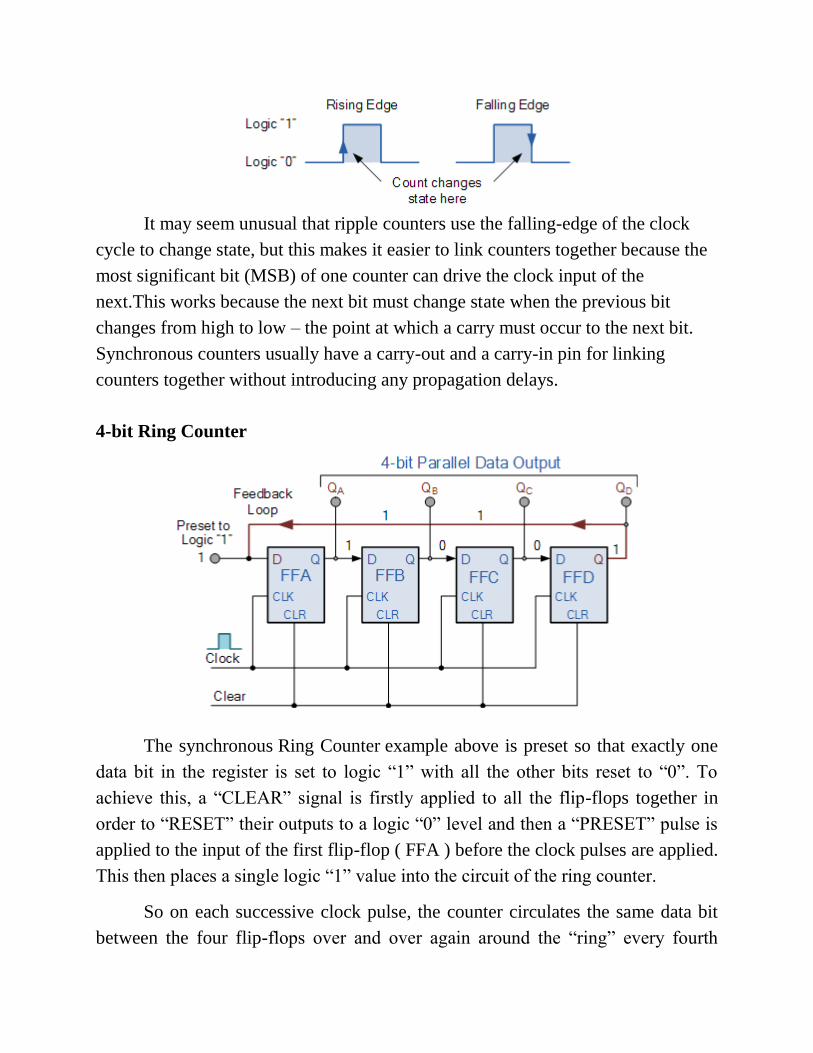
It may seem unusual that ripple counters use the falling-edge of the clock
cycle to change state, but this makes it easier to link counters together because the
most significant bit (MSB) of one counter can drive the clock input of the
next.This works because the next bit must change state when the previous bit
changes from high to low – the point at which a carry must occur to the next bit.
Synchronous counters usually have a carry-out and a carry-in pin for linking
counters together without introducing any propagation delays.
4-bit Ring Counter
The synchronous Ring Counter example above is preset so that exactly one
data bit in the register is set to logic “1” with all the other bits reset to “0”. To
achieve this, a “CLEAR” signal is firstly applied to all the flip-flops together in
order to “RESET” their outputs to a logic “0” level and then a “PRESET” pulse is
applied to the input of the first flip-flop ( FFA ) before the clock pulses are applied.
This then places a single logic “1” value into the circuit of the ring counter.
So on each successive clock pulse, the counter circulates the same data bit
between the four flip-flops over and over again around the “ring” every fourth
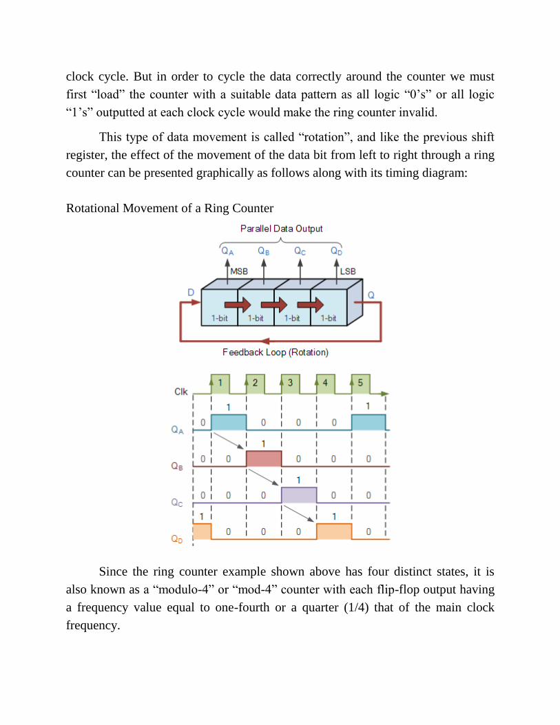
clock cycle. But in order to cycle the data correctly around the counter we must
first “load” the counter with a suitable data pattern as all logic “0’s” or all logic
“1’s” outputted at each clock cycle would make the ring counter invalid.
This type of data movement is called “rotation”, and like the previous shift
register, the effect of the movement of the data bit from left to right through a ring
counter can be presented graphically as follows along with its timing diagram:
Rotational Movement of a Ring Counter
Since the ring counter example shown above has four distinct states, it is
also known as a “modulo-4” or “mod-4” counter with each flip-flop output having
a frequency value equal to one-fourth or a quarter (1/4) that of the main clock
frequency.

The “MODULO” or “MODULUS” of a counter is the number of states the
counter counts or sequences through before repeating itself and a ring counter can
be made to output any modulo number. A “mod-n” ring counter will require “n”
number of flip-flops connected together to circulate a single data bit providing “n”
different output states.
For example, a mod-8 ring counter requires eight flip-flops and a mod-16
ring counter would require sixteen flip-flops. However, as in our example above,
only four of the possible sixteen states are used, making ring counters very
inefficient in terms of their output state usage.
Johnson Ring Counter
The Johnson Ring Counter or “Twisted Ring Counters”, is another shift
register with feedback exactly the same as the standard Ring Counter above, except
that this time the inverted output Q of the last flip-flop is now connected back to
the input D of the first flip-flop as shown below.
The main advantage of this type of ring counter is that it only needs half the
number of flip-flops compared to the standard ring counter then its modulo number
is halved. So a “n-stage” Johnson counter will circulate a single data bit giving
sequence of 2ndifferent states and can therefore be considered as a “mod-2n
counter”.
4-bit Johnson Ring Counter

This inversion of Q before it is fed back to input D causes the counter to
“count” in a different way. Instead of counting through a fixed set of patterns like
the normal ring counter such as for a 4-bit counter, “0001”(1), “0010”(2),
“0100”(4), “1000”(8) and repeat, the Johnson counter counts up and then down as
the initial logic “1” passes through it to the right replacing the preceding logic “0”.
A 4-bit Johnson ring counter passes blocks of four logic “0” and then four
logic “1” thereby producing an 8-bit pattern. As the inverted output Q is connected
to the input D this 8-bit pattern continually repeats. For example, “1000”, “1100”,
“1110”, “1111”, “0111”, “0011”, “0001”, “0000” and this is demonstrated in the
following table below.
Truth Table for a 4-bit Johnson Ring Counter
Clock Pulse
No FFA FFB FFC FFD
0 0 0 0 0
1 1 0 0 0
2 1 1 0 0
3 1 1 1 0
4 1 1 1 1
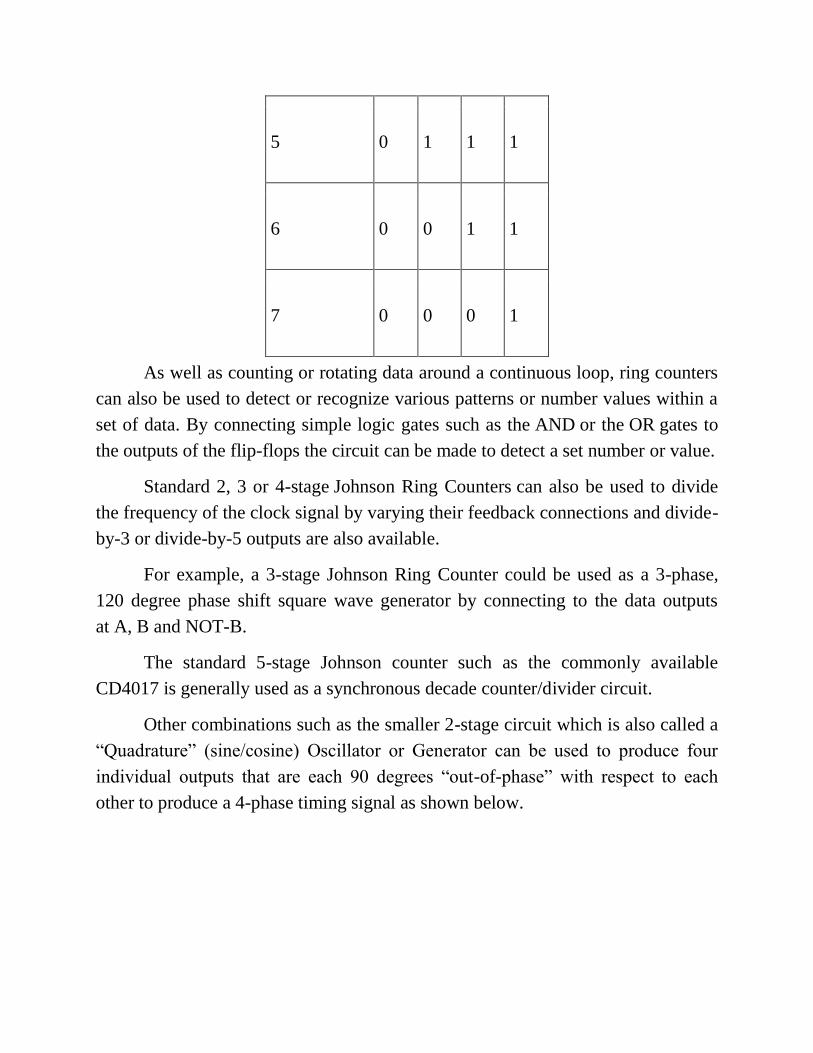
5 0 1 1 1
6 0 0 1 1
7 0 0 0 1
As well as counting or rotating data around a continuous loop, ring counters
can also be used to detect or recognize various patterns or number values within a
set of data. By connecting simple logic gates such as the AND or the OR gates to
the outputs of the flip-flops the circuit can be made to detect a set number or value.
Standard 2, 3 or 4-stage Johnson Ring Counters can also be used to divide
the frequency of the clock signal by varying their feedback connections and divide-
by-3 or divide-by-5 outputs are also available.
For example, a 3-stage Johnson Ring Counter could be used as a 3-phase,
120 degree phase shift square wave generator by connecting to the data outputs
at A, B and NOT-B.
The standard 5-stage Johnson counter such as the commonly available
CD4017 is generally used as a synchronous decade counter/divider circuit.
Other combinations such as the smaller 2-stage circuit which is also called a
“Quadrature” (sine/cosine) Oscillator or Generator can be used to produce four
individual outputs that are each 90 degrees “out-of-phase” with respect to each
other to produce a 4-phase timing signal as shown below.

9. Algorithmic State Machines
Algorithm State Machines(ASM) ASM stands for 'Algorithm State Machine 'or
simply state machine is the another name given to sequential network is used to
control a digital system which carries out a step by a step –by step procedure .It
should be noted that ASM charts represent physical hardware and offers several
advantages.
1. Operation of a digital system can be easily understand by inspection of the SM
chart .
2. ASM charts represent physical hardware.
3. The ASM chart are equivalent to a state graph, and it leads directly to a
hardware realization . 4. ASM charts can be described the operation of both
combinational and sequential circuits .
5. ASM charts are easier to understand and can be converted several equivalent
form.
6. The ASM chart may be equivalently expressed as a state and output table .
10. ASM chart
Principal Component Of An ASM Chart
•State Box.
The state of the system is represented by a state box .It is a rectangular box .At the
top left hand corner the name of state is shown ,which at the top right hand corner
the state assignment is given .Within the state box ,the output signals are listed .

• Decision box .It a diamond –shaped box with true false branches .Boolean
condition is placed in the box and the decision is made from the value of one or
more input signals .The decision box must follow and be associated with a state
Conditional output box .A condition output box is shown in Fig. is a rectangular
box with curved ends .It contain conditional output list .The conditional output
depends on both the state of the system and the inputs .Therefore the conditional
output signals are sometimes known as Mealy output .A condition output must
follow a decision box

Equivalent ASM charts ASM charts are not unique, it may have more than one
equivalent form Fig. shown three equivalent ASM charts for combinational
network Z=A(B+C).
11. control implementation
Conversion Of State Diagram To An ASM Chart
ASM chart can be derived derived an ASM from state diagram of machine ,but
certain rules must be followed when constructing an ASM block. First for every
valid combination of input, there must be exactly one exit path defined .Second ,no
internal feedback within an SM block is allowed.
Mealy Machine.
In case of Mealy machine, output is a function of both present state and input . For
construction of ASM chart from Mealy state diagram, we should follow the
following steps.
1. Represent each state by state boxes.
2. Put input in decision box after each state box.
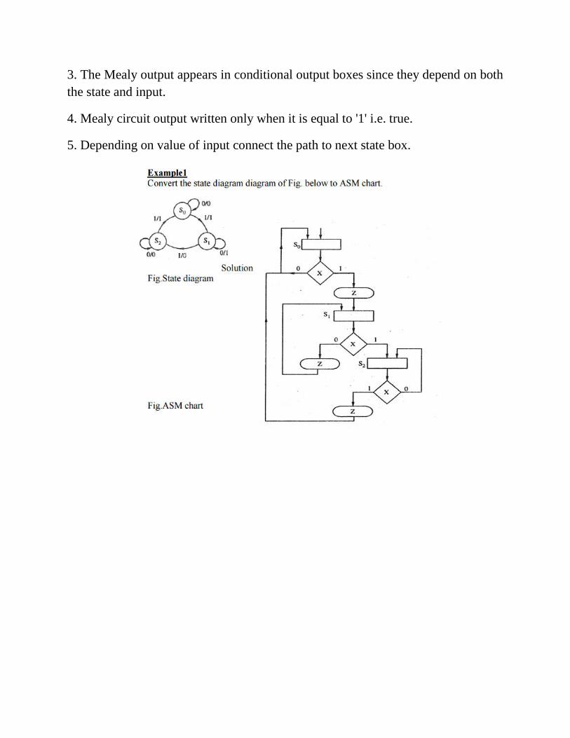
3. The Mealy output appears in conditional output boxes since they depend on both
the state and input.
4. Mealy circuit output written only when it is equal to '1' i.e. true.
5. Depending on value of input connect the path to next state box.

Moore Machine. In case of Moore machine, output is a function of the present state
only . For construction of ASM chart from Moore state diagram, we should follow
the following steps
1. Represent each states by state boxes.
2. The Moore output are placed in the state boxes since they do not depend on the
input .
3. After each state box put the input in decision box.
4. Depending on value of input connect the path to next state box.
Example3 Convert the state diagram of Fig. below to ASM chart.

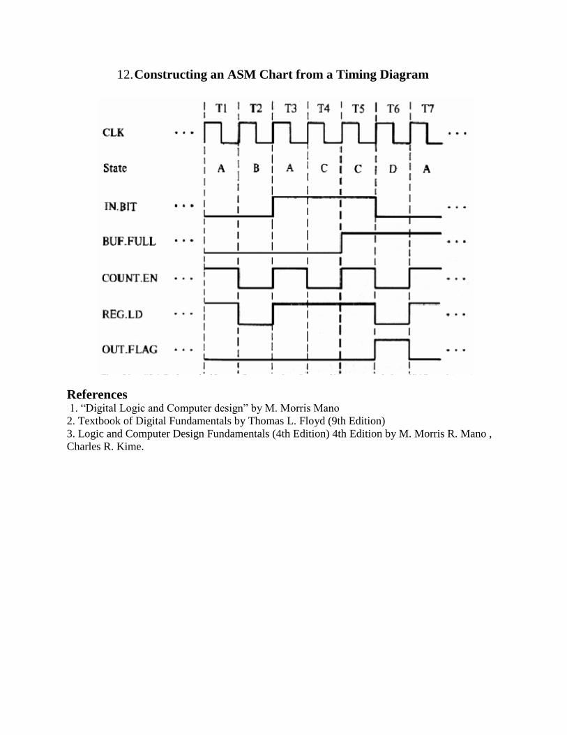
12. Constructing an ASM Chart from a Timing Diagram
References 1. “Digital Logic and Computer design” by M. Morris Mano
2. Textbook of Digital Fundamentals by Thomas L. Floyd (9th Edition)
3. Logic and Computer Design Fundamentals (4th Edition) 4th Edition by M. Morris R. Mano ,
Charles R. Kime.

SCHOOL OF ELECTRICAL AND ELECTRONICS
DEPARTMENT OF ELECTRICAL AND ELECTRONICS
UNIT –V- ASYNCHRONOUS SEQUENTIAL LOGIC AND MEMORY UNIT

UNIT V-
Circuits with Latches - Analysis procedure and Design Procedure - Reduction of state and Flow tables - Race
- Free State Assignment
5.1 SR LATCH
The SR latch is a digital circuit with two inputs s and R and two cross-coupled NOR gates or two cross-coupled
NAND gates.
SR Latch with NOR:
The cross-coupled NOR gate circuit is shown in Fig. (a) This circuit and its truth table are taken from Fig (b) In
order to analyze the circuit by the transition-table method , it is redrawn as fig(c). To see the feedback: path
from the output of gate I to the input of gate 2. The output Q is equivalent to the excitation variable Y and the
secondary variable y, The Boolean function for the output is
Y = [(s + y)' + RI'] (S +y )R' = SR' + R'y

Plotting Y in the Fig. (d). we obtain the transitio n table for table circuit
The state with SR = 10 is a stable stale because Y = y = I; likewise. the state with SR = 0 1 is a sta - ble state.
because Y = y = 0. With SR = 10. the output Q = Y = I and the latch is said to be set. Changing S to 0 leaves the
circuit in the set state . With SR =01 . the output Q = Y = 0 and the latch is said to be reset. A change of R back
to 0 leaves the circuit in the reset state. These conditions are also listed in the truth table. The circuit exhibits
some difficulty when both S and R are equal to 1. From the truth table, we see that both Q and Q' are equal to
0. a condition that violates the requirement that these two outputs be the complement of each other. Moreover,
from the transition table. we note that going from SR = 1 1 and SR = 00 produces an unpredictable result. If S
goes to 0 first. the output remains at 0. but if R goes to 0 first. the output goes to 1. This condition can be
expressed by the Boolean function SR = O. which states that the ANDing of S and R must always result in a 0.
Coming back to the excitation function. we note that when we OR the Boolean expression , SR' with SR. the
result is the single variable S:
SR' + SR = S(R' + R) = S
we infer that SR' = S when SR = 0
Y = SR' + R'y
reduced excitation function Y=S + R'y when SR =0
1.3 SR Latch with NAND:
The NAND latch operates wi th both inputs normally at 1. unless the state of the latch has to be changed . The
application of 0 to R causes the out put Q to goto 0, thus putting the latch in the reset state. After the R input
returns to 1, a change of S to 0 causes a change to the set state. The condition to be avoided here is that both S
and R not be 0 simultaneously. This condition is satisfied when S 'R' =0. The excitation function for the circuit
in Fig.(c1) is
Y - [S(Ry)']' = S' + Ry
Comparing this with the excitation function of the NOR latch. we note that S has been replaced with S' and R'
with R.Hence, the input variables for the NAND latch require the complemented values of those used in the
NOR latch. For this reason. the NAND latch is sometimes referred to as an S'R' latch (or S- R latch).
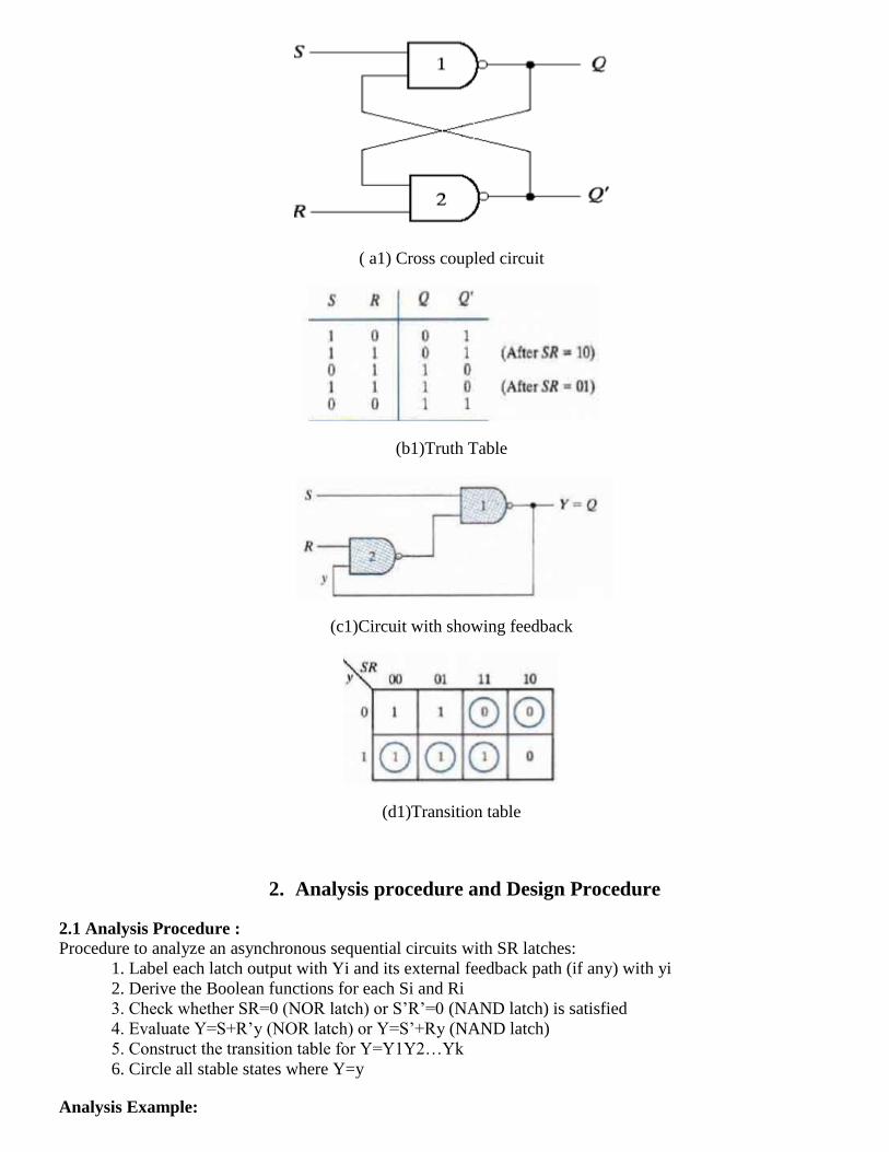
( a1) Cross coupled circuit
(b1)Truth Table
(c1)Circuit with showing feedback
(d1)Transition table
2. Analysis procedure and Design Procedure
2.1 Analysis Procedure :
Procedure to analyze an asynchronous sequential circuits with SR latches:
1. Label each latch output with Yi and its external feedback path (if any) with yi
2. Derive the Boolean functions for each Si and Ri
3. Check whether SR=0 (NOR latch) or S’R’=0 (NAND latch) is satisfied
4. Evaluate Y=S+R’y (NOR latch) or Y=S’+Ry (NAND latch)
5. Construct the transition table for Y=Y1Y2…Yk
6. Circle all stable states where Y=y
Analysis Example:

Asynchronous sequential circuits can be constructed with the use of SR latches with or without external
feedback paths . There is always a feedb ack loop within the latch itself.Th e analysis of a circ uit with latches
will be demonstrated by means of a specific example from which it will be possible to generalize the proced
ural steps necessary to analyze other similar circuits.
The following circuit figure 2 shown here has two SR latches with outputs Y1 and Y2.
Fig 2. Example of a circuit with Srlatches
There are two input x1 and x2. and two external feedback loops giving rise to the secondary varia bles. y1 and
y2,then firs t obtain the Boolean function for the S and R inputs in each latch
We then check whether the condition SR = 0 is satisfied to ensure proper operation of the circuit.
The transition table is given below in figure 3

Fig.3 Transition table
The result is 0 because x1x1’=x2x2’=0
The next step is to derive the transition tab le of the circuit. Remember that thetransition table specifies the
value of Y as a funct ion of y and x. The excitation functions are derived from the relation Y = S + R'y.
2.2 Design Procedure:
1.Obtain a primitive flow table from the given de sign specifications. This is the most difficult pan of the design , because it is necessary to use intuition and experience to arrive at the correct interpretation of the problem specifications. 2.Reduce the flow table by merging rows in the primitive table. 3.Assign binary state variables to eac h row of the reduced flow table to obtain the transition table.
4.Assign outp ut value s to the dashes associ ated with the unstable states to obtain the output maps. 5.Simplify the Boolean functions of the excitation and output variables and draw the logic diagram.
Design Example:
Primitive table:
It is necessary to design a gated latch circuit with two inputs G (gate) and D (data) and one out-put Q. Binary
information present at the D input is transferred to the Q output when G is equal to I. The Q output will follow
the D input as long as G = 1. When G goes to 0, the information that was present at the D input at the time the
transition occurred is retained at the Qoutput. The gated latch is a memory element that accepts the value of D
when G = I and retains this value after G goes to 0. Once G = 0, a change in D does not change the value of the
output Q. The Gated-latch total states is given in Table 1.
2.3 Derive transition table and flow table:
no simultaneous transitions of two variables
state a: after inputs DG=01
state b: after inputs DG=11
only one stable state in each row

Table1 . Gated-latch total states
The primitive flow table for the gated latch is shown in Table 2 . It has one row for each state and one column
for each input combination. First. we fill in one square in each row belonging to the stable state in that row.
These entries are determined from Table 1. For example, State a is stable and the output is 0 when the input is 0
1. This infomation is entered into the flow table in the first row and second column . Similarly. the other five
stable states together with their output are entered into the corresponding input columns.
we can enter dash marks in each row that differs in two or more variables from the input variables associated
with the stable state.For example, the first row in the flow table shows a stable state with an input of 0 1. Since
only one input can change at any given time. it can change to 00 or 11. but not to 10 . Therefore. we enter two
dashes in the 10 column of row a.. This will eventually result in a don' t-care condition for the next state and
output in this square . Following the same procedure, we fill in a second square in each row of the primitive
flow table.
Table 2.Primitive Flow table
2.4 Reduction of the Primitive Flow Table:
Two or more rows in the primitive flow table can be merged if there are nonconflicting states and outputs in
each of columns.
– Primitive flow table is separated into two parts of three rows each in shown in fig 5.
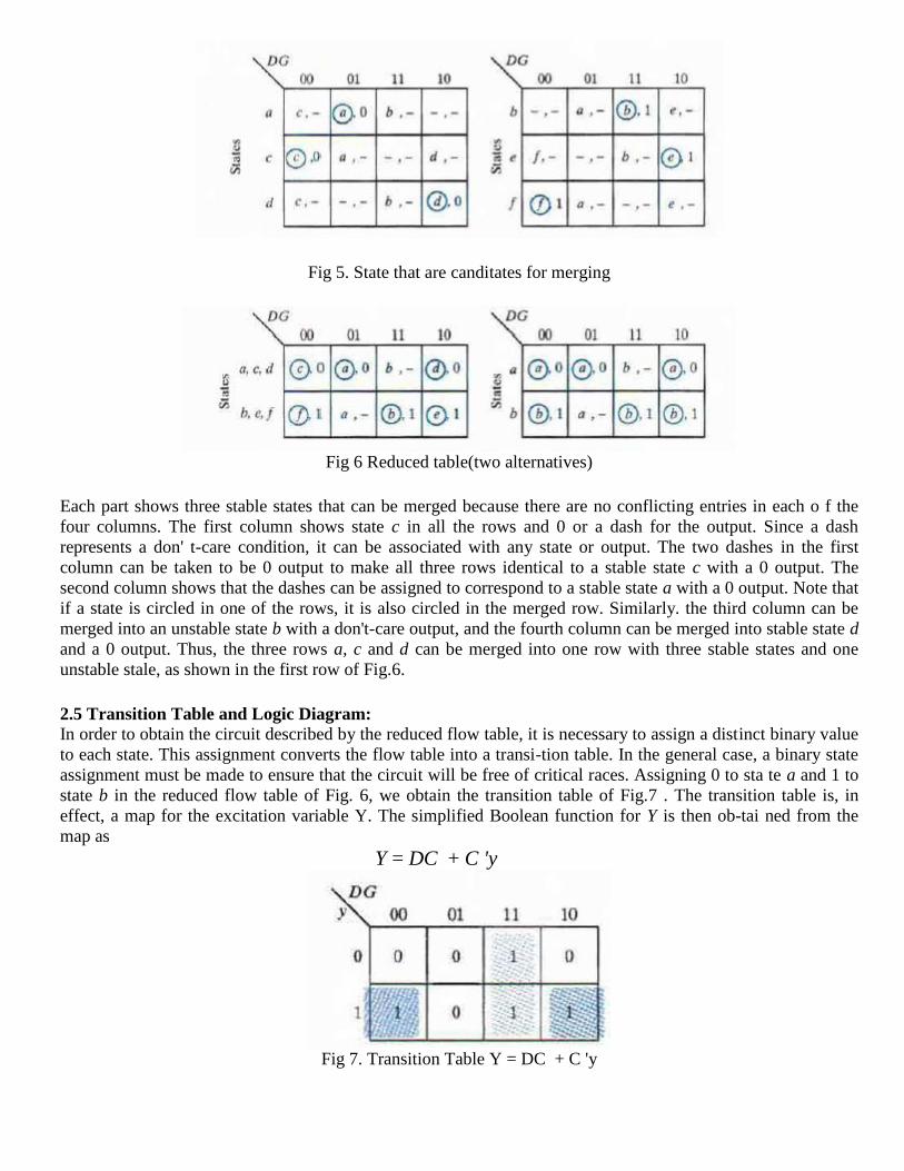
Fig 5. State that are canditates for merging
Fig 6 Reduced table(two alternatives)
Each part shows three stable states that can be merged because there are no conflicting entries in each o f the
four columns. The first column shows state c in all the rows and 0 or a dash for the output. Since a dash
represents a don' t-care condition, it can be associated with any state or output. The two dashes in the first
column can be taken to be 0 output to make all three rows identical to a stable state c with a 0 output. The
second column shows that the dashes can be assigned to correspond to a stable state a with a 0 output. Note that
if a state is circled in one of the rows, it is also circled in the merged row. Similarly. the third column can be
merged into an unstable state b with a don't-care output, and the fourth column can be merged into stable state d
and a 0 output. Thus, the three rows a, c and d can be merged into one row with three stable states and one
unstable stale, as shown in the first row of Fig.6.
2.5 Transition Table and Logic Diagram:
In order to obtain the circuit described by the reduced flow table, it is necessary to assign a distinct binary value
to each state. This assignment converts the flow table into a transi-tion table. In the general case, a binary state
assignment must be made to ensure that the circuit will be free of critical races. Assigning 0 to sta te a and 1 to
state b in the reduced flow table of Fig. 6, we obtain the transition table of Fig.7 . The transition table is, in
effect, a map for the excitation variable Y. The simplified Boolean function for Y is then ob-tai ned from the
map as
Y = DC + C 'y
Fig 7. Transition Table Y = DC + C 'y

There are two don' t-care outputs in the final reduced flow table. If we assign values to the output as shown in
Fig. 8, it is possible to make output Q identical to the map of the excitation function Y.Tthe logic diagram of the
gated latch is as shown in Fig. 9
Fig 8. Output map for gated latch Q=Y
Fig 9. Logic diagram of the gated latch
2.6 Assign Outputs to Unstable States:
The stable states in a flow table have specific output values associated with them. The unstable states have
unspecified output entries designated by a dash. The output values for the unstable states must be chosen so that
no momentary false outputs occur when the circuit switches between stable states. The Flow table and
Output Assignment are shown in fig 10(a) and (b) respectively.
•the unstable states have unspecified output values
•no momentary false outputs occur when circuit switches between stable states
0→0 ==0 : assign 0 if the transient state between two 0 stable states
1→1 = 1 : assign 1 if the transient state between two 1 stable states
0→1, 1→0 = don’t care: assign don’t care if the transient state between two different stable states
Fig 10(a). Flow table (b)Output Assignment
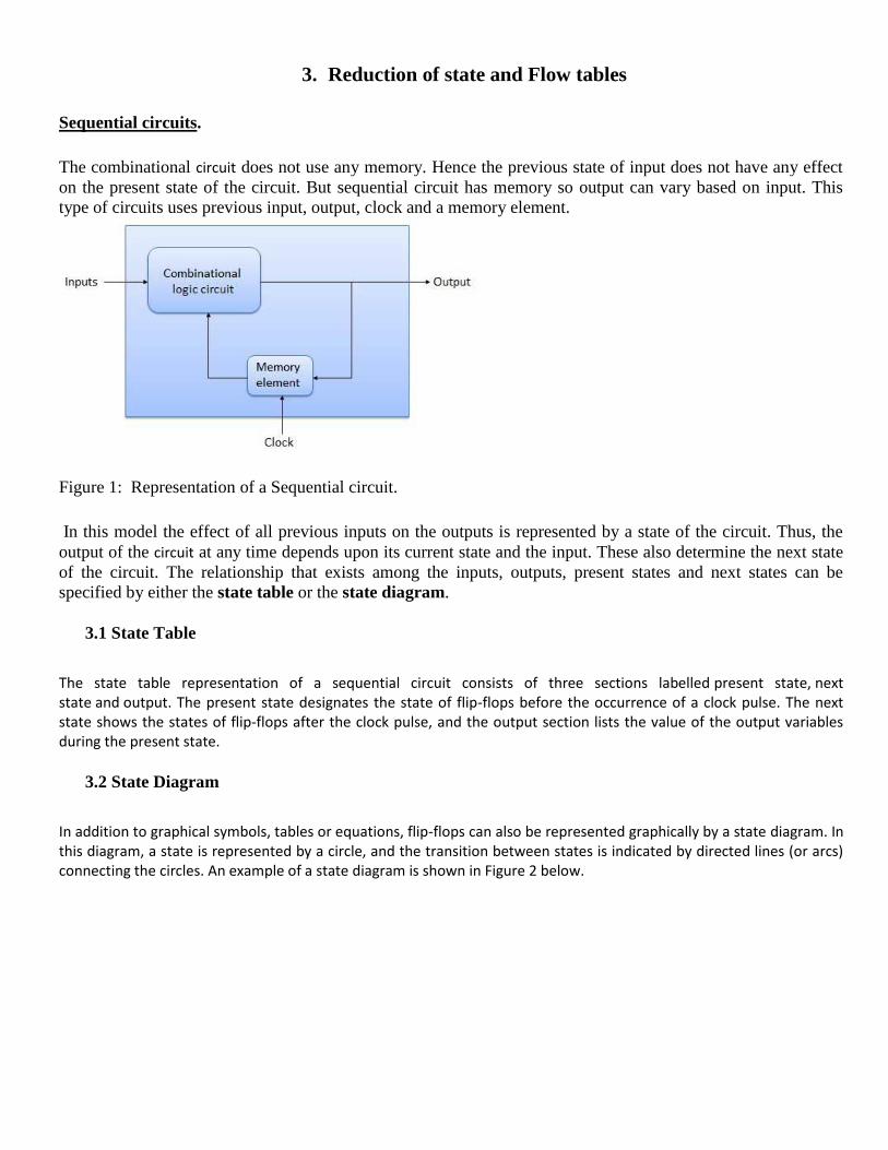
3. Reduction of state and Flow tables
Sequential circuits.
The combinational circuit does not use any memory. Hence the previous state of input does not have any effect
on the present state of the circuit. But sequential circuit has memory so output can vary based on input. This
type of circuits uses previous input, output, clock and a memory element.
Figure 1: Representation of a Sequential circuit.
In this model the effect of all previous inputs on the outputs is represented by a state of the circuit. Thus, the
output of the circuit at any time depends upon its current state and the input. These also determine the next state
of the circuit. The relationship that exists among the inputs, outputs, present states and next states can be
specified by either the state table or the state diagram.
3.1 State Table
The state table representation of a sequential circuit consists of three sections labelled present state, next state and output. The present state designates the state of flip-flops before the occurrence of a clock pulse. The next state shows the states of flip-flops after the clock pulse, and the output section lists the value of the output variables during the present state.
3.2 State Diagram
In addition to graphical symbols, tables or equations, flip-flops can also be represented graphically by a state diagram. In this diagram, a state is represented by a circle, and the transition between states is indicated by directed lines (or arcs) connecting the circles. An example of a state diagram is shown in Figure 2 below.
Figure 2: An example of a state diagram
The binary number inside each circle identifies the state the circle represents. The directed lines are labelled with two binary numbers separated by a slash (/). The input value that causes the state transition is labelled first. The number after the slash symbol / gives the value of the output. For example, the directed line from state 00 to 01 is labelled 1/0, meaning that, if the sequential circuit is in a present state and the input is 1, then the next state is 01 and the output is 0. If it is in a present state 00 and the input is 0, it will remain in that state. A directed line connecting a circle with itself indicates that no change of state occurs. The state diagram provides exactly the same information as the state table and is obtained directly from the state table.
3.3 State Reduction:
The reduction of the number of flip-flops in a sequential circuit is referred to as the state reduction problem. State-reduction algorithms are concerned with procedures for reducing the number of states in a state table, while keeping the external input-output requirements unchanged. Since (N) flip-flops produce (2N) states, a reduction in the number of states may (or may not) result in a reduction in the number of flip-flops. An unpredictable effect in reducing the number of flip-flops is that sometimes the equivalent circuit (with fewer flip-flops) may require more combinational gates. We will illustrate the state reduction procedure with an example. We start with a sequential circuit whose specification is given in the state diagram shown in Figure 3. In this example, only the input-output sequences are important; the internal states are used merely to provide the required sequences. For this reason, the states marked inside the circles are denoted by letter symbols instead of their binary values. This is in constant to a binary counter, where the binary value sequence of the state themselves is taken as the outputs.

Figure 3: State diagram
There are an infinite number of input sequences that may be applied to the circuit; each results in a unique
output sequence. As an example, consider the input sequence [01010110100] starting from the initial state (a).
Each input of 0 or 1 produces an output of 0 or 1 and causes the circuit to go to the next state. the output and
state sequence for the given input sequence as follows: With the circuit in initial state (a), an input of 0 produces
an output of 0 and the circuit remains in state (a). With present state (a) and input of 1, the output is 0 and the
next state is (b). With present state (b) and input of 0, the output is 0 and next state is (c). Continuing this
process, we find the complete sequence to be as follows:
In each column, we have the present state, input value, and output value. The next state is written on top of the
next column. It is important to realize that in this circuit, the states themselves are of secondary importance
because we are interested only in output sequences caused by input sequences. Now let us assume that we have
found a sequential circuit whose state diagram has less than seven states and we wish to compare it with the
circuit whose state diagram is given by Figure 3. If identical input sequences are applied to the two circuits and
identical outputs occur for all input sequences, then the two circuits are said to be equivalent (as far as the input-
output is concerned) and one may be replaced by the other. The problem of state reduction is to find ways of
reducing the number of states in a sequential circuit without altering the input-output relationships. We now
proceed to reduce the number of states for this example. First, we need the state table; it is more convenient to
apply procedures for state reduction using a table rather than a diagram. The state table of the circuit is listed in
Table 1 and is obtained directly from the state diagram.

Table 1: State table
An algorithm for the state reduction of a completely specified state table is given here without proof:"Two
states are said to be equivalent if, for each member of the set of inputs, they give exactly the same output and
send the circuit either to the same state or to an equivalent state." When two states are equivalent, one of them
can be removed without altering the input-output relationships. Now apply this algorithm to Table 1. Going
through the state table, we look for two present states that go to the same next state and have the same output
for both input combinations. States (g) and (e) are two such states: one of these states can be removed. The
procedure of removing a state and replacing it by its equivalent is demonstrated in Table 2. The row with
present state (g) is removed and state (g) is replaced by state (e) each time it occurs in the next-state columns.
Table 2: Reducing the State table
Table 3: Reduced State table

Figure 4: Reduced State diagram
Present state (f) now has next states (e and f) and outputs 0 and 1 for x=0 and x=1, respectively. The same next
states and outputs appear in the row with present (d). Therefore, states (f and d) are equivalent and state (f) can
be removed and replaced by (d). The final reduced table is shown in Table 3. The state diagram for the reduced
table consists of only five states and is shown in Figure 4. This state diagram satisfies the original input-output
specifications and will produce the required output sequence for any given input sequence. The following list
derived from the state diagram of Figure 4 is for the input sequence used previously (note that the same output
sequence results, although the state sequence is different):
Infact, this sequence is exactly the same as that obtained for Figure 3, if we replace (g by e and f by d).
Checking each pair of states for possible equivalency can be done systematically by means of a procedure that
employs an implication table. The implication table consists of squares, one for every suspected pair of possible
equivalent states. By judicious use of the table, it is possible to determine all pairs of equivalent states in a state
table. The use of the implication table for reducing the number of states in a state table is demonstrated in the
next section. The sequential circuit of this example was reduced from seven to five state. In general, reducing
the number of states in a state table may result in a circuit with less equipment. However, the fact that a state
table has been reduced to fewer state doesn't guarantee a saving in the number of flip-flops or the number of
gates.
Example 1: Consider a sequential circuit shown in Figure 5. It has one input x, one output Z and two state
variables Q1Q2 (thus having four possible present states 00, 01, 10, 11).

Figure 5: A sequential circuit
The behaviour of the circuit is determined by the following Boolean expressions:
Z = x*Q1
D1 = x' + Q1
D2 = x*Q2' + x'*Q1'
These equations can be used to form the state table. Suppose the present state (i.e. Q1Q2) = 00 and input x = 0.
Under these conditions, we get Z = 0, D1 = 1, and D2 = 1. Thus the next state of the circuit D1D2 = 11, and this
will be the present state after the clock pulse has been applied. The output of the circuit corresponding to the
present state Q1Q2 = 00 and x = 1 is Z = 0. This data is entered into the state table as shown in Table 4.
Table 4: State table for the sequential circuit in Figure 5.
The state diagram for the sequential circuit in Figure 5 is shown in Figure 6.

Figure 6: State Diagram of circuit in Figure 5.
3.4 Implication Table:
The state-reduction procedure for completely specified state tables is based on the algorithm that two states in a
state table can be combined into one if they can be shown to be equivalent. Two states are equivalent if for each
possible input, they give exactly the same output and go to the same next states or to equivalent next state.
Consider for example, the state table shown in Table 5. The present states (a) and (b) have the same output for
the same input. Their next states are (c and d) for x=0 and (b and a) for x=1. If we can show that the pair of
states (c, d) are equivalent, then the pair of states (a, b) will also be equivalent because they will have the same
or equivalent next states. When this relationship exists, we say that (a, b) imply (c, d). Similarly, from the last
two rows of Table 5, we find that the pair of states (c, d) imply the pair of states (a, b). The characteristic of
equivalent states is that if (a, b) imply (c, d) and (c, d) imply (a, b), then both pairs of states are equivalent; that
is, (a and b) are equivalent as well as (c and d). As a consequence, the four rows of Table 5 can be reduced to
two rows by combining (a and b) into one state and (c and d) into a second state.
The checking of each pair of states for possible equivalence in a table with a large number of states can
be done systematically by means of an implication table. The implication table is a chart that consists of
squares, one for every possible pair of states, that provide spaces for listing any possible implied states. By
judicious use of the table, it is possible to determine all pairs of equivalent states. The state table of Table 6 will
be used to illustrate this procedure. The implication table is shown in Figure 7. On the left side along the
vertical are listed all the states defined in the state table except the first, and across the bottom horizontally are
listed all the states expect the last. The result is a display of all possible combinations of two states with a square
placed in the intersection of a row and a column where the two states can be tested for equivalence. Two states
that are not equivalent are marked with a cross (x) in the corresponding square, whereas their equivalence
recorded with a check mark (√). Some of the squares have entries of implied states that must be further
investigated to determine whether they are equivalent or not. The step-by-step procedure of filling in the
squares is as follows. First, we place a cross in any square corresponding to a pair of states whose outputs are
not equal for every input. In this case, state (c) has a different output than any other state, so a cross is placed in
the two squares of row (c) and the four squares of column (c). There are nine other squares in this category in
the implication table.

Table 5: State Table to Demonstrate Equivalent States.
Next, we enter in the remaining squares the pairs of states that are implied by the pair of states representing the
squares. We do that starting from the top square in the left column and going down and then proceeding with
the next column to the right. From the state table, we see that pair (a,b) imply (d,e), so (d,e) is recorded in the
square defined by column (a and row b). We proceed in this manner until the entire table is completed. Note
that states (d,e) are equivalent because they go to the same next state and have the some output. Therefore, a
check mark is recorded in the square defined by column (d and row e), indicating that the two states are
equivalent and independent of any implied pair. The next step is to make successive passes through the table to
determine whether any additional squares should be marked with a cross. A square in the table is crossed out if
it contains at least one implied pair that is not equivalent. For example, the square defined by (a) and (f) is
marked with a cross next to (c,d) because the pair (c,d) defines a square that contains a cross. This procedure is
repeated until no additional squares can be crossed out.
Finally, all the squares that have no crosses are recorded with check marks. These squares define pairs of
equivalent states. In this example, the equivalent states are: (a,b) (d,e) (d,g) (e,g).
Table 6: State Table to be Reduced.
Figure 7: Implication table.
We now combine pairs of states into larger groups of equivalent states. The last three pairs can be combined
into a set of three equivalent states (d,e,g) because each one of the states in the group is equivalent to the other
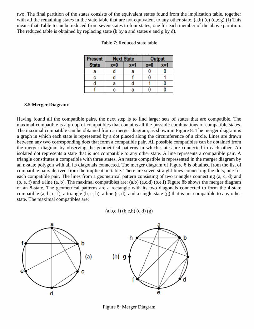
two. The final partition of the states consists of the equivalent states found from the implication table, together
with all the remaining states in the state table that are not equivalent to any other state. (a,b) (c) (d,e,g) (f) This
means that Table 6 can be reduced from seven states to four states, one for each member of the above partition.
The reduced table is obtained by replacing state (b by a and states e and g by d).
Table 7: Reduced state table
3.5 Merger Diagram:
Having found all the compatible pairs, the next step is to find larger sets of states that are compatible. The
maximal compatible is a group of compatibles that contains all the possible combinations of compatible states.
The maximal compatible can be obtained from a merger diagram, as shown in Figure 8. The merger diagram is
a graph in which each state is represented by a dot placed along the circumference of a circle. Lines are drawn
between any two corresponding dots that form a compatible pair. All possible compatibles can be obtained from
the merger diagram by observing the geometrical patterns in which states are connected to each other. An
isolated dot represents a state that is not compatible to any other state. A line represents a compatible pair. A
triangle constitutes a compatible with three states. An nstate compatible is represented in the merger diagram by
an n-state polygon with all its diagonals connected. The merger diagram of Figure 8 is obtained from the list of
compatible pairs derived from the implication table. There are seven straight lines connecting the dots, one for
each compatible pair. The lines from a geometrical pattern consisting of two triangles connecting (a, c, d) and
(b, e, f) and a line (a, b). The maximal compatibles are: (a,b) (a,c,d) (b,e,f) Figure 8b shows the merger diagram
of an 8-state. The geometrical patterns are a rectangle with its two diagonals connected to form the 4-state
compatible (a, b, e, f), a triangle (b, c, h), a line (c, d), and a single state (g) that is not compatible to any other
state. The maximal compatibles are:
(a,b,e,f) (b,c,h) (c,d) (g)
Figure 8: Merger Diagram

3.6 Reduction of flow table
Reduction of primitive flow table has two functions: Elimination of redundant stable states, Merging those
stable states which are distinguishable by input states.
Let 00 = a; 01 = b; 11 = c; 01 = d
00 = a
01 = b
11 = c
01 = d
The resulting flow table is
4. Race‐Free State Assignment A race condition is caused when two or more binary state variables change value due to change in an input
variable
Unequal delays may cause state variables to change in unpredictable manner
Race condition may be (i) non- critical, or (ii) critical
(i) Non critical race

Possible transitions
00->11
00->01->11
00->10->11
(ii) Critical race
Possible transitions
00->11
00->01
00->10
Once a reduced flow table has been derived, the next step in the design is to assign binary variables to each
stable state. The main objective in choosing a proper binary state assignment is the prevention of critical races.
Adjacent Binary Values: 2 binary values are said to be adjacent if they differ in only one variable ( e.g. 010 and
011 are adjacent).
2‐Row Flow‐Table: The assignment of a single variable to a flow table with two rows does not impose
critical race problems. [two adjacent adjacent values 0 and 1]
3‐Row Flow‐Table :
Example: A flow table with 3 states requires an assignment of 2 variables. • We have the following
transitions: a -> b, a -> c, b -> a, b -> c & c -> a (see the transition diagram in figure 9.
Figure 9: (a)Flow table (b) Transition diagram
If we take the following assignment:

This assignment will cause a critical race during the transition from a to c (2 changes in the binary state ), and
also from c to a.
A race‐free assignment can be obtained by adding an extra row to the original flow table : The use of an extra
row will not increase the number of binary state variables (2 variables), but it allows the formation of cycles
between two stable states. The added row (d) is assigned the binary value (10), which is adjacent to both a & c.
The transition from a to c must go through d, thus avoiding a critical race. The two squares with dashes in row d
represent unspecified states (don’t care). These squares must not be assigned to 01 in order to avoid the
possibility of stable state being established in the 4th row. Then the corresponding flow table and transition
diagram will be shown in figure 10.
Figure 10: (a) Flow table (b) Transition diagram
The new flow table is converted to a transition table to complete the design process
Figure 11: (a) Flow table (b) Transition table