Embed Size (px)
Citation preview

managementMEDIAHEALTH
lawD
ESIGN
EDU
CAT
ION
MU
SICagriculture
LA
NG
UA
GEM E C H A N I C S
psychology
BIOTECHNOLOGY
GEOGRAPHY
ARTPHYSICS
history
ECOLOGY
CHEMISTRY
math
ematicsENGINEERING
Fundamentals of Assembly Language
Subject: FUNDAMENTALS OF ASSEMBLY LANGUAGE Credits: 4
SYLLABUS
The Computer and its Components History of Computing, Data representation, Number System, Fixed Point Number Representation, Floating Point Number Representation, BCD representation, Error Detection Code, Fixed and Instruction execution, Interrupts,Buses, Boolean Algebra, Logic Circuits, Logic Gates, Combinational circuits, Sequential Circuit, Adders, Decoders, Multiplexer, Encoder, Types Of Flip Flop, Edge Triggered, Master-Slave, Asynchronous (Serial Or Ripple) Counters, Shift Register Memory System Memory Hierarchy, RAM, DRAM, SRAM, ROM,Flash Memory, Secondary memory, Optical Memories, Hard disk drives, Head Mechanisms, CCDs, Bubble memories, RAID, Cache Organisation, Memory System of Micro-Computers, Input/ Output System, DMA, Input output processors, External Communication Interfaces, Interrupt Processing, BUS arbitration, Floppy Drives, CD-ROM, DVD-ROM, Cartridge Drives, Recordable CDs, CD-RW, Input/ Output Technologies, Characteristics, Video Cards, Monitors, USB Port, Liquid Crystal Display (LCD), Sound Cards, Modems, Printers, Scanner, Digital Cameras, Keyboard, Mouse, Power supply. Central Processing Unit The Instruction and instruction Set, Addressing modes and their importance, Register, Micro-operation, Description of Various types of Registers with the help of a Microprocessor example, ALU, Control Unit, Hardwired Control, Wilkes control, Micro-programmed control, Microinstructions, Assembly Language Programming Microprocessor, Instruction format for an example Microprocessor, The need and use of assembly language, Input output in assembly Language Program, Assembly Programming tools, Interfacing assembly with HLL, Device Deriver of assembly language, Interrupts in assembly language programming, Suggested Reading: Verma, G.; Mielke, N. Reliability performance of ETOX based flash memories. IEEE International
Reliability Physics Symposium.
Doron D. Swade . Redeeming Charles Babbage's Mechanical Computer. Scientific American
Meuer, Hans; Strohmaier, Erich; Simon, Horst; Dongarra, Jack . "Architectures Share Over Time". TOP500.
Lavington, Simon . A History of Manchester Computers (2 ed.). Swindon: The British Computer Society
Stokes, Jon . Inside the Machine: An Illustrated Introduction to Microprocessors and Computer Architecture. San Francisco: No Starch Press. Zuse, Konrad . The Computer - My life. Berlin: Pringler-Verlag.
Fundamentals of Assembly Language
1.1 The computer and its components
A computer is a general purpose device that can be programmed to carry out a set of arithmetic or logical operations. Since a sequence of operations can be readily changed, the computer can solve more than one kind of problem.
Conventionally, a computer consists of at least one processing element, typically a central processing unit (CPU) and some form of memory. The processing element carries out arithmetic and logic operations, and a sequencing and control unit that can change the order of operations based on stored information. Peripheral devices allow information to be retrieved from an external source, and the result of operations saved and retrieved.
The first electronic digital computers were developed between 1940 and 1945. Originally they were the size of a large room, consuming as much power as several hundred modern personal computers (PCs). In this era mechanical analog computers were used for military applications.
Modern computers based on integrated circuits are millions to billions of times more capable than the early machines, and occupy a fraction of the space. Simple computers are small enough to fit into mobile devices, and mobile computers can be powered by small batteries. Personal computers in their various forms are icons of the Information Age and are what most people think of as ―computers.‖ However, the embedded computers found in many devices from MP3 players to fighter aircraft and from toys to industrial robots are the most numerous.
1.1.1 Components
A general purpose computer has four main components: the arithmetic logic unit (ALU), the control unit, the memory, and the input and output devices (collectively termed I/O). These parts are interconnected by buses, often made of groups of wires.
Inside each of these parts are thousands to trillions of small electrical circuits which can be turned off or on by means of an electronic switch. Each circuit represents a bit (binary digit) of information so that when the circuit is on it represents a ―1‖, and when off it represents a ―0‖ (in
positive logic representation). The circuits are arranged in logic gates so that one or more of the circuits may control the state of one or more of the other circuits.
The control unit, ALU, registers, and basic I/O (and often other hardware closely linked with these) are collectively known as a central processing unit (CPU). Early CPUs were composed of many separate components but since the mid-1970s CPUs have typically been constructed on a single integrated circuit called a microprocessor.
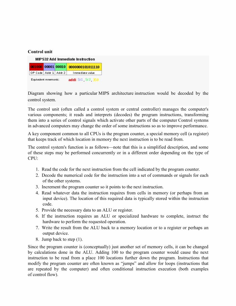
Control unit
Diagram showing how a particular MIPS architecture instruction would be decoded by the control system.
The control unit (often called a control system or central controller) manages the computer's various components; it reads and interprets (decodes) the program instructions, transforming them into a series of control signals which activate other parts of the computer Control systems in advanced computers may change the order of some instructions so as to improve performance.
A key component common to all CPUs is the program counter, a special memory cell (a register) that keeps track of which location in memory the next instruction is to be read from.
The control system's function is as follows—note that this is a simplified description, and some of these steps may be performed concurrently or in a different order depending on the type of CPU:
1. Read the code for the next instruction from the cell indicated by the program counter. 2. Decode the numerical code for the instruction into a set of commands or signals for each
of the other systems. 3. Increment the program counter so it points to the next instruction. 4. Read whatever data the instruction requires from cells in memory (or perhaps from an
input device). The location of this required data is typically stored within the instruction code.
5. Provide the necessary data to an ALU or register. 6. If the instruction requires an ALU or specialized hardware to complete, instruct the
hardware to perform the requested operation. 7. Write the result from the ALU back to a memory location or to a register or perhaps an
output device. 8. Jump back to step (1).
Since the program counter is (conceptually) just another set of memory cells, it can be changed by calculations done in the ALU. Adding 100 to the program counter would cause the next instruction to be read from a place 100 locations further down the program. Instructions that modify the program counter are often known as ―jumps‖ and allow for loops (instructions that
are repeated by the computer) and often conditional instruction execution (both examples of control flow).
The sequence of operations that the control unit goes through to process an instruction is in itself like a short computer program, and indeed, in some more complex CPU designs, there is another yet smaller computer called a microsequencer, which runs a microcode program that causes all of these events to happen.
1.1.1.1 Arithmetic logic unit (ALU)
The ALU is capable of performing two classes of operations: arithmetic and logic.
The set of arithmetic operations that a particular ALU supports may be limited to addition and subtraction, or might include multiplication, division, trigonometry functions such as sine, cosine, etc., and square roots. Some can only operate on whole numbers (integers) whilst others use floating point to represent real numbers, albeit with limited precision. However, any computer that is capable of performing just the simplest operations can be programmed to break down the more complex operations into simple steps that it can perform. Therefore, any computer can be programmed to perform any arithmetic operation—although it will take more time to do so if its ALU does not directly support the operation. An ALU may also compare numbers and returnboolean truth values (true or false) depending on whether one is equal to, greater than or less than the other (―is 64 greater than 65?‖).
Logic operations involve Boolean logic: AND, OR, XOR and NOT. These can be useful for creating complicated conditional statements and processing boolean logic.
Superscalar computers may contain multiple ALUs, allowing them to process several instructions simultaneously. Graphics processors and computers with SIMD and MIMD features often contain ALUs that can perform arithmetic on vectors and matrices.
1.1.1.2 Memory A computer's memory can be viewed as a list of cells into which numbers can be placed or read. Each cell has a numbered ―address‖ and can store a single number. The computer can be instructed to ―put the number 123 into the cell numbered 1357‖ or to ―add the number that is in
cell 1357 to the number that is in cell 2468 and put the answer into cell 1595.‖ The information
stored in memory may represent practically anything. Letters, numbers, even computer instructions can be placed into memory with equal ease. Since the CPU does not differentiate between different types of information, it is the software's responsibility to give significance to what the memory sees as nothing but a series of numbers.
In almost all modern computers, each memory cell is set up to store binary numbers in groups of eight bits (called a byte). Each byte is able to represent 256 different numbers (2^8 = 256); either from 0 to 255 or −128 to +127. To store larger numbers, several consecutive bytes may be used
(typically, two, four or eight). When negative numbers are required, they are usually stored in two's complement notation. Other arrangements are possible, but are usually not seen outside of specialized applications or historical contexts. A computer can store any kind of information in memory if it can be represented numerically. Modern computers have billions or even trillions of bytes of memory.
The CPU contains a special set of memory cells called registers that can be read and written to much more rapidly than the main memory area. There are typically between two and one hundred registers depending on the type of CPU. Registers are used for the most frequently needed data items to avoid having to access main memory every time data is needed. As data is constantly being worked on, reducing the need to access main memory (which is often slow compared to the ALU and control units) greatly increases the computer's speed.
Computer main memory comes in two principal varieties: random-access memory or RAM and read-only memory or ROM. RAM can be read and written to anytime the CPU commands it, but ROM is preloaded with data and software that never changes, therefore the CPU can only read from it. ROM is typically used to store the computer's initial start-up instructions. In general, the contents of RAM are erased when the power to the computer is turned off, but ROM retains its data indefinitely. In a PC, the ROM contains a specialized program called the BIOS that orchestrates loading the computer's operating system from the hard disk drive into RAM whenever the computer is turned on or reset. In embedded computers, which frequently do not have disk drives, all of the required software may be stored in ROM. Software stored in ROM is often called firmware, because it is notionally more like hardware than software. Flash memory blurs the distinction between ROM and RAM, as it retains its data when turned off but is also rewritable. It is typically much slower than conventional ROM and RAM however, so its use is restricted to applications where high speed is unnecessary.
In more sophisticated computers there may be one or more RAM cache memories, which are slower than registers but faster than main memory. Generally computers with this sort of cache are designed to move frequently needed data into the cache automatically, often without the need for any intervention on the programmer's part.
1.1.1.3 Input/output (I/O) I/O is the means by which a computer exchanges information with the outside world. Devices that provide input or output to the computer are calledperipherals. On a typical personal computer, peripherals include input devices like the keyboard and mouse, and output devices such as the displayand printer. Hard disk drives, floppy disk drives and optical disc drives serve as both input and output devices. Computer networking is another form of I/O.
I/O devices are often complex computers in their own right, with their own CPU and memory. A graphics processing unit might contain fifty or more tiny computers that perform the calculations necessary to display 3D graphics.[citation needed] Modern desktop computers contain many smaller computers that assist the main CPU in performing I/O.
1.1.1.4 Multitasking While a computer may be viewed as running one gigantic program stored in its main memory, in some systems it is necessary to give the appearance of running several programs simultaneously. This is achieved by multitasking i.e. having the computer switch rapidly between running each program in turn. One means by which this is done is with a special signal called an interrupt, which can periodically cause the computer to stop executing instructions where it was and do something else instead. By remembering where it was executing prior to the interrupt, the
computer can return to that task later. If several programs are running ―at the same time,‖ then
the interrupt generator might be causing several hundred interrupts per second, causing a program switch each time. Since modern computers typically execute instructions several orders of magnitude faster than human perception, it may appear that many programs are running at the same time even though only one is ever executing in any given instant. This method of multitasking is sometimes termed ―time-sharing‖ since each program is allocated a ―slice‖ of
time in turn
Before the era of cheap computers, the principal use for multitasking was to allow many people to share the same computer.
Seemingly, multitasking would cause a computer that is switching between several programs to run more slowly, in direct proportion to the number of programs it is running, but most programs spend much of their time waiting for slow input/output devices to complete their tasks. If a program is waiting for the user to click on the mouse or press a key on the keyboard, then it will not take a ―time slice‖ until the event it is waiting for has occurred. This frees up time for other
programs to execute so that many programs may be run simultaneously without unacceptable speed loss.
1.1.1.5 Multiprocessing Some computers are designed to distribute their work across several CPUs in a multiprocessing configuration, a technique once employed only in large and powerful machines such as supercomputers, mainframe computers and servers. Multiprocessor and multi-core (multiple CPUs on a single integrated circuit) personal and laptop computers are now widely available, and are being increasingly used in lower-end markets as a result.
Supercomputers in particular often have highly unique architectures that differ significantly from the basic stored-program architecture and from general purpose computers.[53] They often feature thousands of CPUs, customized high-speed interconnects, and specialized computing hardware. Such designs tend to be useful only for specialized tasks due to the large scale of program organization required to successfully utilize most of the available resources at once. Supercomputers usually see usage in large-scale simulation, graphics rendering, and cryptography applications, as well as with other so-called ―embarrassingly parallel‖ tasks.
1.1.1.6 Networking and the Internet Computers have been used to coordinate information between multiple locations since the 1950s. The U.S. military's SAGE system was the first large-scale example of such a system, which led to a number of special-purpose commercial systems such asSabre.
In the 1970s, computer engineers at research institutions throughout the United States began to link their computers together using telecommunications technology. The effort was funded by ARPA (now DARPA), and the computer network that resulted was called the ARPANET. The technologies that made the Arpanet possible spread and evolved.
In time, the network spread beyond academic and military institutions and became known as the Internet. The emergence of networking involved a redefinition of the nature and boundaries of
the computer. Computer operating systems and applications were modified to include the ability to define and access the resources of other computers on the network, such as peripheral devices, stored information, and the like, as extensions of the resources of an individual computer. Initially these facilities were available primarily to people working in high-tech environments, but in the 1990s the spread of applications like e-mail and the World Wide Web, combined with the development of cheap, fast networking technologies like Ethernet andADSL saw computer networking become almost ubiquitous. In fact, the number of computers that are networked is growing phenomenally. A very large proportion of personal computers regularly connect to the Internet to communicate and receive information. ―Wireless‖ networking, often utilizing mobile
phone networks, has meant networking is becoming increasingly ubiquitous even in mobile computing environments.
1.2 History of Computing
The first use of the word ―computer‖ was recorded in 1613 in a book called ―The yong mans
gleanings‖ by English writer Richard Braithwait I haue read the truest computer of Times, and the best Arithmetician that euer breathed, and he reduceth thy dayes into a short number. It referred to a person who carried out calculations, or computations, and the word continued with the same meaning until the middle of the 20th century. From the end of the 19th century the word began to take on its more familiar meaning, a machine that carries out computations.
1.2.1 Limited-function early computers The history of the modern computer begins with two separate technologies, automated calculation and programmability. However no single device can be identified as the earliest computer, partly because of the inconsistent application of that term. A few devices are worth mentioning though, like somemechanical aids to computing, which were very successful and survived for centuries until the advent of the electronic calculator, like the Sumerian abacus, designed around 2500 BC of which a descendant won a speed competition against a contemporary desk calculating machine in Japan in 1946 theslide rules, invented in the 1620s, which were carried on five Apollo space missions, including to the moon and arguably the astrolabe and theAntikythera mechanism, an ancient astronomical analog computer built by the Greeks around 80 BC The Greek mathematician Hero of Alexandria (c. 10–70 AD) built a mechanical theater which performed a play lasting 10 minutes and was operated by a complex system of ropes and drums that might be considered to be a means of deciding which parts of the mechanism performed which actions and when. This is the essence of programmability.
Blaise Pascal invented the mechanical calculator in 1642, known as Pascal's calculator, it was the first machine to better human performance of arithmetical computations and would turn out to be the only functional mechanical calculator in the 17th century. Two hundred years later, in 1851,Thomas de Colmar released, after thirty years of development, his simplified arithmometer; it became the first machine to be commercialized because it was strong enough and reliable enough to be used daily in an office environment. The mechanical calculator was at the root of the development of computers in two separate ways. Initially, it was in trying to develop more powerful and more flexible calculators[12] that the computer was first theorized by Charles Babbage and then developed. Secondly, development of a low-cost electronic calculator,
successor to the mechanical calculator, resulted in the development by Intel of the first commercially availablemicroprocessor integrated circuit.
1.2.2 First general-purpose computers In 1801, Joseph Marie Jacquard made an improvement to the textile loom by introducing a series of punched paper cards as a template which allowed his loom to weave intricate patterns automatically. The resulting Jacquard loom was an important step in the development of computers because the use of punched cards to define woven patterns can be viewed as an early, albeit limited, form of programmability.
It was the fusion of automatic calculation with programmability that produced the first recognizable computers. In 1837, Charles Babbage was the first to conceptualize and design a fully programmablemechanical computer, his analytical engine. Limited finances and Babbage's inability to resist tinkering with the design meant that the device was never completed—
nevertheless his son, Henry Babbage, completed a simplified version of the analytical engine's computing unit (the mill) in 1888. He gave a successful demonstration of its use in computing tables in 1906. This machine was given to the Science museum in South Kensington in 1910.
Between 1842 and 1843, Ada Lovelace, an analyst of Charles Babbage's analytical engine, translated an article by Italian military engineer Luigi Menabrea on the engine, which she supplemented with an elaborate set of notes of her own, simply called Notes. These notes contain what is considered the first computer program – that is, an algorithm encoded for processing by a machine. Lovelace's notes are important in the early history of computers. She also developed a vision on the capability of computers to go beyond mere calculating or number-crunching while others, including Babbage himself, focused only on those capabilities.
In the late 1880s, Herman Hollerith invented the recording of data on a machine-readable medium. Earlier uses of machine-readable media had been for control, not data. ―After some
initial trials with paper tape, he settled on punched cards... To process these punched cards he invented the tabulator, and the keypunch machines. These three inventions were the foundation of the modern information processing industry. Large-scale automated data processing of punched cards was performed for the 1890 United States Census by Hollerith's company, which later became the core of IBM. By the end of the 19th century a number of ideas and technologies, that would later prove useful in the realization of practical computers, had begun to appear:Boolean algebra, the vacuum tube (thermionic valve), punched cards and tape, and the teleprinter.
During the first half of the 20th century, many scientific computing needs were met by increasingly sophisticatedanalog computers, which used a direct mechanical or electrical model of the problem as a basis forcomputation. However, these were not programmable and generally lacked the versatility and accuracy of modern digital computers.
Alan Turing is widely regarded as the father of modern computer science. In 1936, Turing provided an influential formalization of the concept of the algorithmand computation with the Turing machine, providing a blueprint for the electronic digital computer.[23] Of his role in the creation of the modern computer,Time magazine in naming Turing one of the 100 most influential people of the 20th century, states: ―The fact remains that everyone who taps at a
keyboard, opening a spreadsheet or a word-processing program, is working on an incarnation of a Turing machine.
The first really functional computer was the Z1, originally created by Germany's Konrad Zuse in his parents living room in 1936 to 1938, and it is considered to be the first electro-mechanical binary programmable (modern) computer.
George Stibitz is internationally recognized as a father of the modern digital computer. While working at Bell Labs in November 1937, Stibitz invented and built a relay-based calculator he dubbed the ―Model K‖ (for ―kitchen table,‖ on which he had assembled it), which was the first to
usebinary circuits to perform an arithmetic operation. Later models added greater sophistication including complex arithmetic and programmability.
The Atanasoff–Berry Computer (ABC) was the world's first electronic digital computer, albeit not programmable. Atanasoff is considered to be one of the fathers of the computer. Conceived in 1937 by Iowa State College physics professor John Atanasoff, and built with the assistance of graduate student Clifford Berry,[28] the machine was not programmable, being designed only to solve systems of linear equations. The computer did employ parallel computation. A 1973 court ruling in a patent dispute found that the patent for the 1946 ENIAC computer derived from the Atanasoff–Berry Computer.
The first program-controlled computer was invented by Konrad Zuse, who built the Z3, an electromechanical computing machine, in 1941. The first programmable electronic computer was the Colossus, built in 1943 by Tommy Flowers.
1.2.3 Key steps towards modern computers A succession of steadily more powerful and flexible computing devices were constructed in the 1930s and 1940s, gradually adding the key features that are seen in modern computers. The use of digital electronics (largely invented by Claude Shannon in 1937) and more flexible programmability were vitally important steps, but defining one point along this road as ―the first
digital electronic computer‖ is difficult.
Notable achievements include:
Konrad Zuse's electromechanical ―Z machines.‖ The Z3 (1941) was the first working machine featuring binary arithmetic, including floating point arithmetic and a measure of programmability. In 1998 the Z3 was proved to be Turing complete, therefore being the world's first operational computer. Thus, Zuse is often regarded as the inventor of the computer.
The non-programmable Atanasoff–Berry Computer (commenced in 1937, completed in 1941) which used vacuum tube based computation, binary numbers, and regenerative capacitor memory. The use of regenerative memory allowed it to be much more compact than its peers (being approximately the size of a large desk or workbench), since intermediate results could be stored and then fed back into the same set of computation elements.
The secret British Colossus computers (1943), which had limited programmability but demonstrated that a device using thousands of tubes could be reasonably reliable and electronically re-programmable. It was used for breaking German wartime codes.
The Harvard Mark I (1944), a large-scale electromechanical computer with limited programmability.
The U.S. Army's Ballistic Research Laboratory ENIAC (1946), which used decimal arithmetic and is sometimes called the first general purposeelectronic computer (since Konrad Zuse's Z3 of 1941 used electromagnets instead of electronics). Initially, however, ENIAC had an architecture which required rewiring a plugboard to change its programming.
1.2.4 Stored-program architecture Several developers of ENIAC, recognizing its flaws, came up with a far more flexible and elegant design, which came to be known as the ―stored-program architecture‖ or von Neumann architecture. This design was first formally described by John von Neumann in the paper First Draft of a Report on the EDVAC, distributed in 1945. A number of projects to develop computers based on the stored-program architecture commenced around this time, the first of which was completed in 1948 at the University of Manchester in England, the Manchester Small-Scale Experimental Machine (SSEM or ―Baby‖). The Electronic Delay Storage Automatic Calculator (EDSAC), completed a year after the SSEM at Cambridge University, was the first practical, non-experimental implementation of the stored-program design and was put to use immediately for research work at the university. Shortly thereafter, the machine originally described by von Neumann's paper—EDVAC—was completed but did not see full-time use for an additional two years. Nearly all modern computers implement some form of the stored-program architecture, making it the single trait by which the word ―computer‖ is now defined. While the technologies used in
computers have changed dramatically since the first electronic, general-purpose computers of the 1940s, most still use the von Neumann architecture.
Beginning in the 1950s, Soviet scientists Sergei Sobolev and Nikolay Brusentsov conducted research on ternary computers, devices that operated on a base three numbering system of -1, 0, and 1 rather than the conventional binary numbering system upon which most computers are based. They designed the Setun, a functional ternary computer, at Moscow State University. The device was put into limited production in the Soviet Union, but supplanted by the more common binary architecture.
1.2.5 Semiconductors and microprocessors Computers using vacuum tubes as their electronic elements were in use throughout the 1950s, but by the 1960s they had been largely replaced bytransistor-based machines, which were smaller, faster, cheaper to produce, required less power, and were more reliable. The first transistorized computer was demonstrated at the University of Manchester in 1953. In the 1970s, integrated circuit technology and the subsequent creation ofmicroprocessors, such as the Intel 4004, further decreased size and cost and further increased speed and reliability of computers. By the late 1970s, many products such as video recorders contained dedicated
computers called microcontrollers, and they started to appear as a replacement to mechanical controls in domestic appliances such as washing machines. The 1980s witnessed home computers and the now ubiquitous personal computer. With the evolution of the Internet, personal computers are becoming as common as the television and the telephone in the household Modern smartphones are fully programmable computers in their own right, and as of 2009 may well be the most common form of such computers in existence.]
Programs
The defining feature of modern computers which distinguishes them from all other machines is that they can be programmed. That is to say that some type of instructions (the program) can be given to the computer, and it will process them. Modern computers based on the von Neumann architectureoften have machine code in the form of an imperative programming language.In practical terms, a computer program may be just a few instructions or extend to many millions of instructions, as do the programs for word processors and web browsers for example. A typical modern computer can execute billions of instructions per second (gigaflops) and rarely makes a mistake over many years of operation. Large computer programs consisting of several million instructions may take teams of programmers years to write, and due to the complexity of the task almost certainly contain errors.
Stored program architecture This section applies to most common RAM machine-based computers.
In most cases, computer instructions are simple: add one number to another, move some data from one location to another, send a message to some external device, etc. These instructions are read from the computer's memory and are generally carried out (executed) in the order they were given. However, there are usually specialized instructions to tell the computer to jump ahead or backwards to some other place in the program and to carry on executing from there. These are called ―jump‖ instructions (or branches). Furthermore, jump instructions may be made to happen conditionally so that different sequences of instructions may be used depending on the result of some previous calculation or some external event. Many computers directly support subroutines by providing a type of jump that ―remembers‖ the location it jumped from and another instruction to return to the instruction following that jump instruction.
Program execution might be likened to reading a book. While a person will normally read each word and line in sequence, they may at times jump back to an earlier place in the text or skip sections that are not of interest. Similarly, a computer may sometimes go back and repeat the instructions in some section of the program over and over again until some internal condition is met. This is called the flow of control within the program and it is what allows the computer to perform tasks repeatedly without human intervention.
Comparatively, a person using a pocket calculator can perform a basic arithmetic operation such as adding two numbers with just a few button presses. But to add together all of the numbers from 1 to 1,000 would take thousands of button presses and a lot of time, with a near certainty of making a mistake. On the other hand, a computer may be programmed to do this with just a few simple instructions. For example:
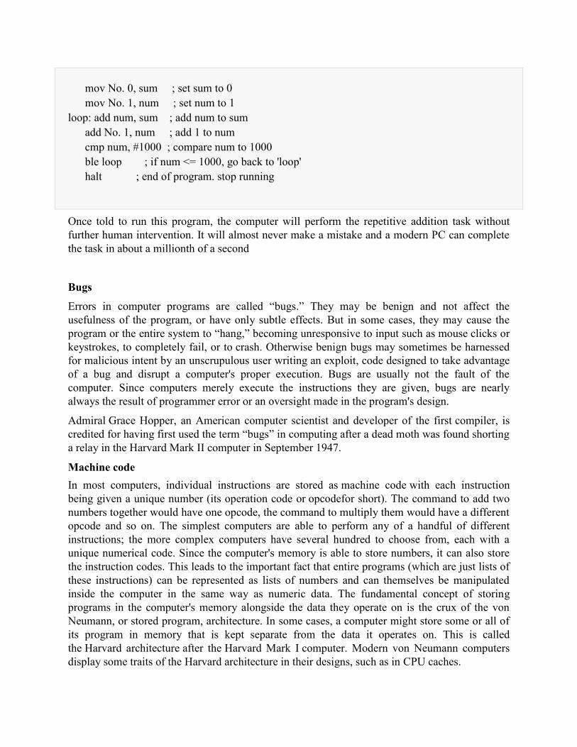
mov No. 0, sum ; set sum to 0 mov No. 1, num ; set num to 1 loop: add num, sum ; add num to sum add No. 1, num ; add 1 to num cmp num, #1000 ; compare num to 1000 ble loop ; if num <= 1000, go back to 'loop' halt ; end of program. stop running
Once told to run this program, the computer will perform the repetitive addition task without further human intervention. It will almost never make a mistake and a modern PC can complete the task in about a millionth of a second
Bugs
Errors in computer programs are called ―bugs.‖ They may be benign and not affect the
usefulness of the program, or have only subtle effects. But in some cases, they may cause the program or the entire system to ―hang,‖ becoming unresponsive to input such as mouse clicks or keystrokes, to completely fail, or to crash. Otherwise benign bugs may sometimes be harnessed for malicious intent by an unscrupulous user writing an exploit, code designed to take advantage of a bug and disrupt a computer's proper execution. Bugs are usually not the fault of the computer. Since computers merely execute the instructions they are given, bugs are nearly always the result of programmer error or an oversight made in the program's design.
Admiral Grace Hopper, an American computer scientist and developer of the first compiler, is credited for having first used the term ―bugs‖ in computing after a dead moth was found shorting
a relay in the Harvard Mark II computer in September 1947.
Machine code In most computers, individual instructions are stored as machine code with each instruction being given a unique number (its operation code or opcodefor short). The command to add two numbers together would have one opcode, the command to multiply them would have a different opcode and so on. The simplest computers are able to perform any of a handful of different instructions; the more complex computers have several hundred to choose from, each with a unique numerical code. Since the computer's memory is able to store numbers, it can also store the instruction codes. This leads to the important fact that entire programs (which are just lists of these instructions) can be represented as lists of numbers and can themselves be manipulated inside the computer in the same way as numeric data. The fundamental concept of storing programs in the computer's memory alongside the data they operate on is the crux of the von Neumann, or stored program, architecture. In some cases, a computer might store some or all of its program in memory that is kept separate from the data it operates on. This is called the Harvard architecture after the Harvard Mark I computer. Modern von Neumann computers display some traits of the Harvard architecture in their designs, such as in CPU caches.
While it is possible to write computer programs as long lists of numbers (machine language) and while this technique was used with many early computers, it is extremely tedious and potentially error-prone to do so in practice, especially for complicated programs. Instead, each basic instruction can be given a short name that is indicative of its function and easy to remember – a mnemonic such as ADD, SUB, MULT or JUMP. These mnemonics are collectively known as a computer's assembly language. Converting programs written in assembly language into something the computer can actually understand (machine language) is usually done by a computer program called an assembler.
Programming language
Programming languages provide various ways of specifying programs for computers to run. Unlike natural languages, programming languages are designed to permit no ambiguity and to be concise. They are purely written languages and are often difficult to read aloud. They are generally either translated into machine code by a compiler or an assembler before being run, or translated directly at run time by an interpreter. Sometimes programs are executed by a hybrid method of the two techniques.
Low-level languages
Machine languages and the assembly languages that represent them (collectively termed low-level programming languages) tend to be unique to a particular type of computer. For instance, an ARM architecture computer (such as may be found in a PDA or a hand-held videogame) cannot understand the machine language of an Intel Pentium or the AMD Athlon 64 computer that might be in a PC.
Higher-level languages
Though considerably easier than in machine language, writing long programs in assembly language is often difficult and is also error prone. Therefore, most practical programs are written in more abstract high-level programming languages that are able to express the needs of the programmer more conveniently (and thereby help reduce programmer error). High level languages are usually ―compiled‖ into machine language (or sometimes into assembly language and then into machine language) using another computer program called a compiler. High level languages are less related to the workings of the target computer than assembly language, and more related to the language and structure of the problem(s) to be solved by the final program. It is therefore often possible to use different compilers to translate the same high level language program into the machine language of many different types of computer. This is part of the means by which software like video games may be made available for different computer architectures such as personal computers and various video game consoles.
Program design Program design of small programs is relatively simple and involves the analysis of the problem, collection of inputs, using the programming constructs within languages, devising or using established procedures and algorithms, providing data for output devices and solutions to the problem as applicable. As problems become larger and more complex, features such as subprograms, modules, formal documentation, and new paradigms such as object-oriented programming are encountered. Large programs involving thousands of line of code and more require formal software methodologies. The task of developing large software systems presents a significant intellectual challenge. Producing software with an acceptably high reliability within a predictable schedule and budget has historically been difficult; the academic and professional discipline of software engineering concentrates specifically on this challenge.
1.3 Data representation
Computers can sense when an electrical signal being sent is either on or off. This is represented by a '1' (on) or a '0' (off). Each individual 1 or 0 is called a binary digit or bit and it is the smallest piece of data that a computer system can work with.
Eight bits are grouped together to make one byte.
One byte provides enough codes (256) to represent all of the characters that appear on a standard keyboard. A byte is the basic unit used to measure computer memory size.
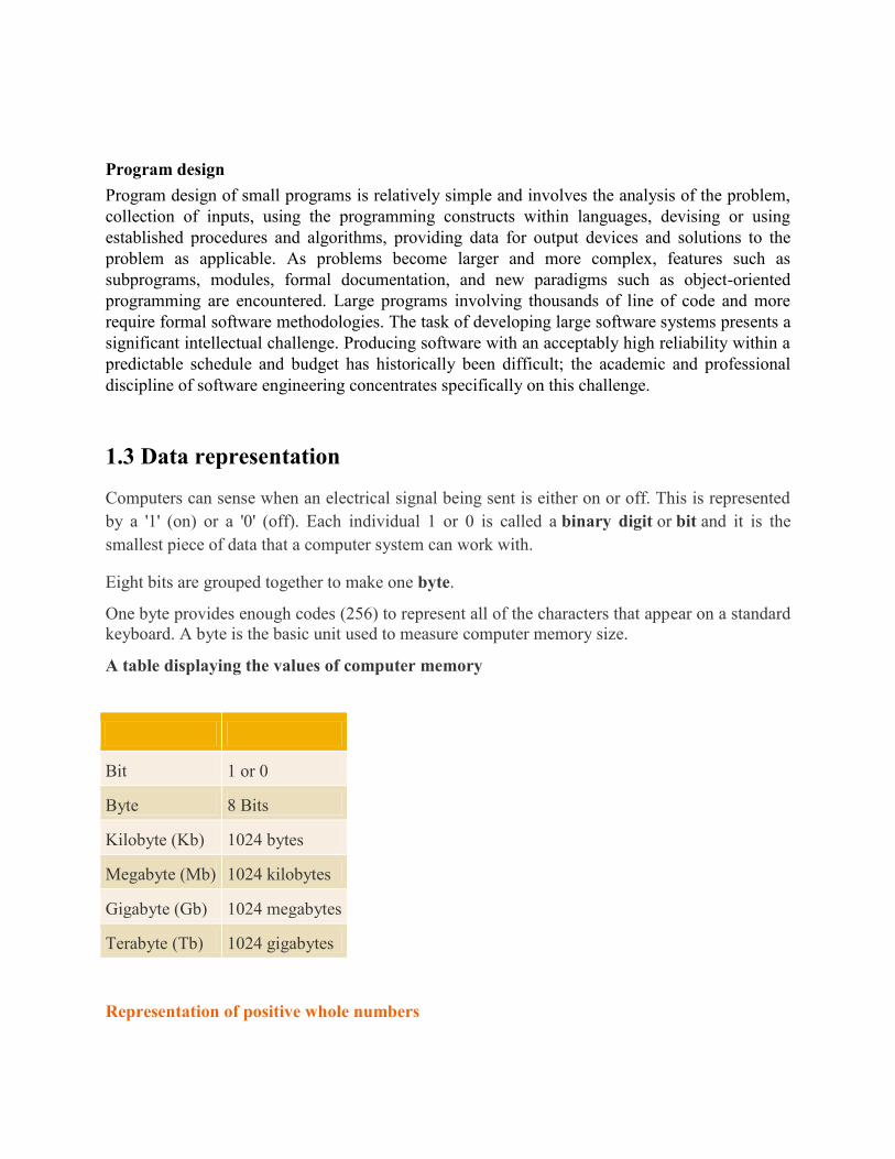
A table displaying the values of computer memory
Bit 1 or 0
Byte 8 Bits
Kilobyte (Kb) 1024 bytes
Megabyte (Mb) 1024 kilobytes
Gigabyte (Gb) 1024 megabytes
Terabyte (Tb) 1024 gigabytes
Representation of positive whole numbers
We can represent any number, however large, in binary. Remember we can only store numbers between 0 and 255 in one byte. This is obviously rather restrictive since it's not dealing with large integers, negative numbers or decimal numbers.
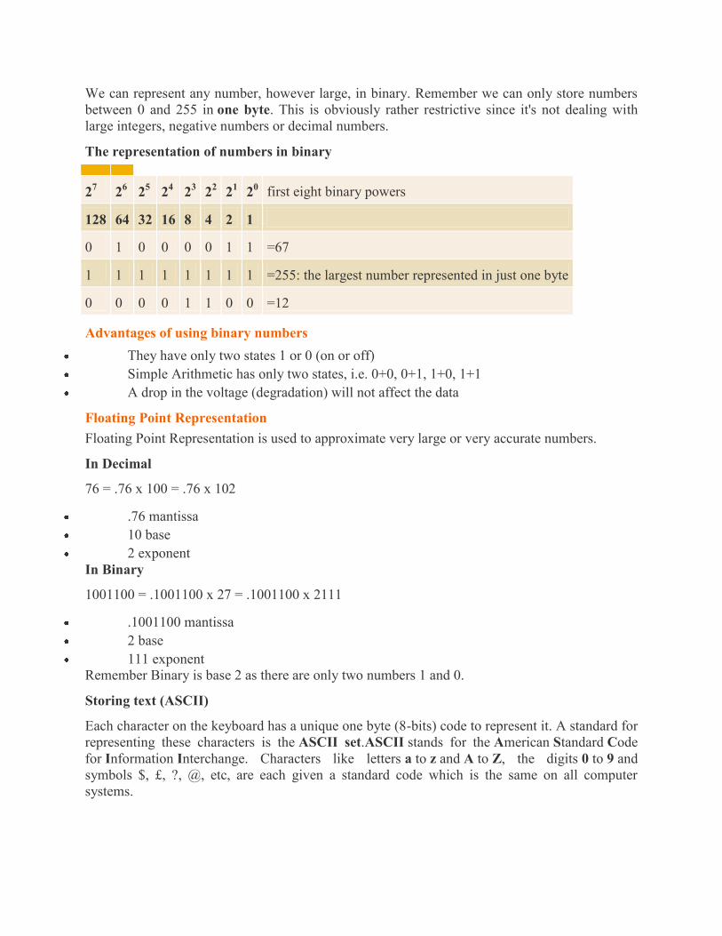
The representation of numbers in binary
27 26 25 24 23 22 21 20 first eight binary powers
128 64 32 16 8 4 2 1
0 1 0 0 0 0 1 1 =67
1 1 1 1 1 1 1 1 =255: the largest number represented in just one byte
0 0 0 0 1 1 0 0 =12
Advantages of using binary numbers They have only two states 1 or 0 (on or off) Simple Arithmetic has only two states, i.e. 0+0, 0+1, 1+0, 1+1 A drop in the voltage (degradation) will not affect the data
Floating Point Representation Floating Point Representation is used to approximate very large or very accurate numbers.
In Decimal
76 = .76 x 100 = .76 x 102
.76 mantissa 10 base 2 exponent
In Binary
1001100 = .1001100 x 27 = .1001100 x 2111
.1001100 mantissa 2 base 111 exponent
Remember Binary is base 2 as there are only two numbers 1 and 0.
Storing text (ASCII)
Each character on the keyboard has a unique one byte (8-bits) code to represent it. A standard for representing these characters is the ASCII set.ASCII stands for the American Standard Code for Information Interchange. Characters like letters a to z and A to Z, the digits 0 to 9 and symbols $, £, ?, @, etc, are each given a standard code which is the same on all computer systems.
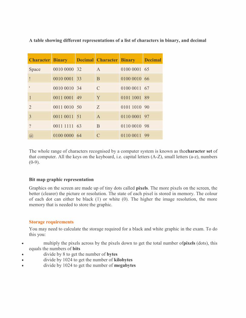
A table showing different representations of a list of characters in binary, and decimal
Character Binary Decimal Character Binary Decimal
Space 0010 0000 32 A 0100 0001 65
! 0010 0001 33 B 0100 0010 66
' 0010 0010 34 C 0100 0011 67
1 0011 0001 49 Y 0101 1001 89
2 0011 0010 50 Z 0101 1010 90
3 0011 0011 51 A 0110 0001 97
? 0011 1111 63 B 0110 0010 98
@ 0100 0000 64 C 0110 0011 99
The whole range of characters recognised by a computer system is known as thecharacter set of that computer. All the keys on the keyboard, i.e. capital letters (A-Z), small letters (a-z), numbers (0-9).
Bit map graphic representation
Graphics on the screen are made up of tiny dots called pixels. The more pixels on the screen, the better (clearer) the picture or resolution. The state of each pixel is stored in memory. The colour of each dot can either be black (1) or white (0). The higher the image resolution, the more memory that is needed to store the graphic.
Storage requirements You may need to calculate the storage required for a black and white graphic in the exam. To do this you:
multiply the pixels across by the pixels down to get the total number ofpixels (dots), this equals the numbers of bits
divide by 8 to get the number of bytes divide by 1024 to get the number of kilobytes divide by 1024 to get the number of megabytes
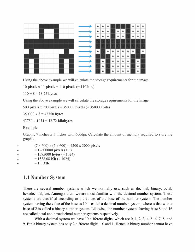
Using the above example we will calculate the storage requirements for the image.
10 pixels x 11 pixels = 110 pixels (= 110 bits)
110 ÷ 8 = 13.75 bytes
Using the above example we will calculate the storage requirements for the image.
500 pixels x 700 pixels = 350000 pixels (= 350000 bits)
350000 ÷ 8 = 43750 bytes
43750 ÷ 1024 = 42.72 kilobytes
Example
Graphic 7 inches x 5 inches with 600dpi. Calculate the amount of memory required to store the graphic.
(7 x 600) x (5 x 600) = 4200 x 3000 pixels = 12600000 pixels (÷ 8) = 1575000 bytes (÷ 1024) = 1538.08 Kb (÷ 1024) = 1.5 Mb
1.4 Number System There are several number systems which we normally use, such as decimal, binary, octal, hexadecimal, etc. Amongst them we are most familiar with the decimal number system. These systems are classified according to the values of the base of the number system. The number system having the value of the base as 10 is called a decimal number system, whereas that with a base of 2 is called a binary number system. Likewise, the number systems having base 8 and 16 are called octal and hexadecimal number systems respectively.
With a decimal system we have 10 different digits, which are 0, 1, 2, 3, 4, 5, 6, 7, 8, and 9. But a binary system has only 2 different digits—0 and 1. Hence, a binary number cannot have
any digit other than 0 or 1. So to deal with a binary number system is quite easier than a decimal system. Now, in a digital world, we can think in binary nature, e.g., a light can be either off or on. There is no state in between these two. So we generally use the binary system when we deal with the digital world. Here comes the utility of a binary system. We can express everything in the world with the help of only two digits i.e., 0 and 1. For example, if we want to express 2510 in binary we may write 110012. The right most digit in a number system is called the ‗Least
Significant Bit‘ (LSB) or ‗Least Significant Digit‘ (LSD). And the left most digit in a number
system is called the ‗Most Significant Bit‘ (MSB) or ‗Most Significant Digit‘ (MSD). Now
normally when we deal with different number systems we specify the base as the subscript to make it clear which number system is being used.
In an octal number system there are 8 digits—0, 1, 2, 3, 4, 5, 6, and 7. Hence, any octal number cannot have any digit greater than 7. Similarly, a hexadecimal number system has 16 digits—0 to 9— and the rest of the six digits are specified by letter symbols as A, B, C, D, E, and F. Here A, B, C, D, E, and F represent decimal 10, 11, 12, 13, 14, and 15 respectively. Octal and hexadecimal codes are useful to write assembly level language.
In general, we can express any number in any base or radix ―X.‖ Any number with base
X, having n digits to the left and m digits to the right of the decimal point can be expressed as:
anXn-1 + an-1Xn-2 + an-2Xn-3 + …. + a2X1 + a1X0 + b1X-1 + b2X-2 + …. + bmX-m where an is the digit in the nth position. The coefficient an is termed as the MSD or Most Significant Digit and bm is termed as the LSD or the Least Significant Digit. 1.4.1 Conversion between Number System It is often required to convert a number in a particular number system to any other number system, e.g., it may be required to convert a decimal number to binary or octal or hexadecimal. The reverse is also true, i.e., a binary number may be converted into decimal and so on. The methods of interconversions are now discussed. 1.4.1.1 Decimal-to-Binary Conversion Now to convert a number in decimal to a number in binary we have to divide the decimal number by 2 repeatedly, until the quotient of zero is obtained. This method of repeated division by 2 is called the ‗double-dabble‘ method. The remainders are noted down for each of the division steps. Then the column of the remainder is read in reverse order i.e., from bottom to top order. We try to show the method with an example shown in Example 1.1.
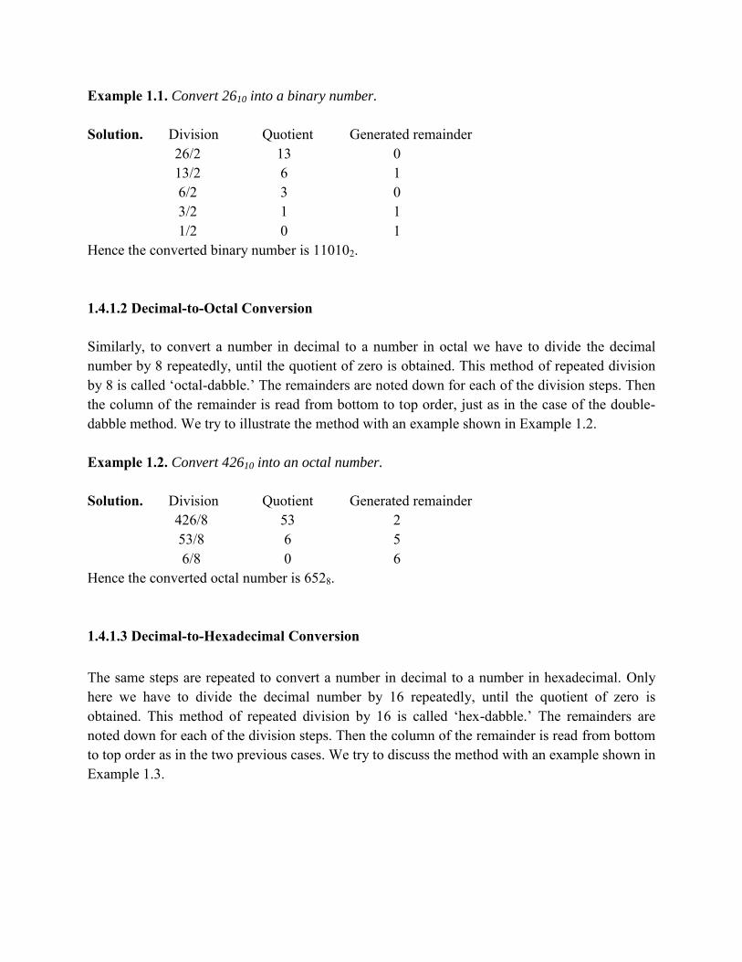
Example 1.1. Convert 2610 into a binary number.
Solution. Division Quotient Generated remainder 26/2 13 0 13/2 6 1 6/2 3 0 3/2 1 1 1/2 0 1 Hence the converted binary number is 110102. 1.4.1.2 Decimal-to-Octal Conversion Similarly, to convert a number in decimal to a number in octal we have to divide the decimal number by 8 repeatedly, until the quotient of zero is obtained. This method of repeated division by 8 is called ‗octal-dabble.‘ The remainders are noted down for each of the division steps. Then the column of the remainder is read from bottom to top order, just as in the case of the double-dabble method. We try to illustrate the method with an example shown in Example 1.2. Example 1.2. Convert 42610 into an octal number.
Solution. Division Quotient Generated remainder 426/8 53 2 53/8 6 5 6/8 0 6 Hence the converted octal number is 6528. 1.4.1.3 Decimal-to-Hexadecimal Conversion The same steps are repeated to convert a number in decimal to a number in hexadecimal. Only here we have to divide the decimal number by 16 repeatedly, until the quotient of zero is obtained. This method of repeated division by 16 is called ‗hex-dabble.‘ The remainders are noted down for each of the division steps. Then the column of the remainder is read from bottom to top order as in the two previous cases. We try to discuss the method with an example shown in Example 1.3.
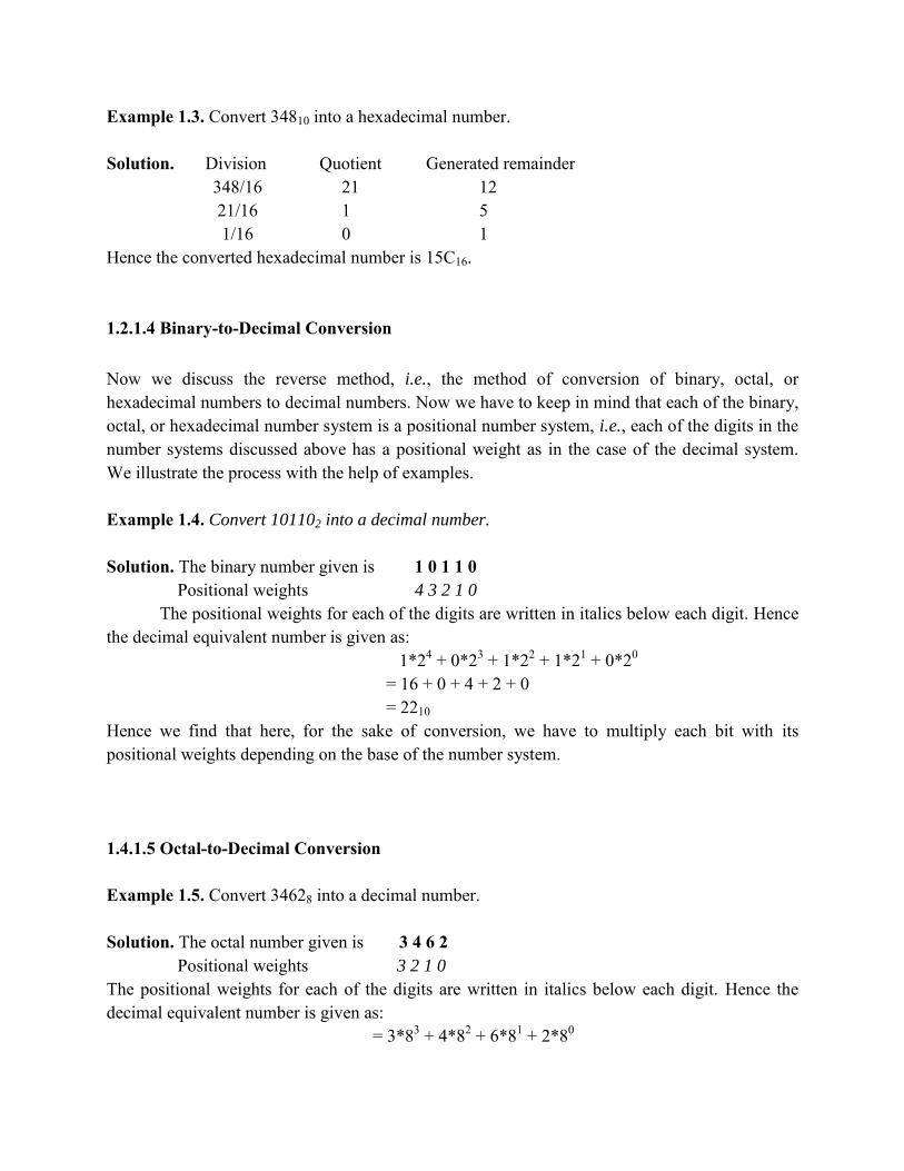
Example 1.3. Convert 34810 into a hexadecimal number. Solution. Division Quotient Generated remainder 348/16 21 12 21/16 1 5 1/16 0 1 Hence the converted hexadecimal number is 15C16. 1.2.1.4 Binary-to-Decimal Conversion Now we discuss the reverse method, i.e., the method of conversion of binary, octal, or hexadecimal numbers to decimal numbers. Now we have to keep in mind that each of the binary, octal, or hexadecimal number system is a positional number system, i.e., each of the digits in the number systems discussed above has a positional weight as in the case of the decimal system. We illustrate the process with the help of examples. Example 1.4. Convert 101102 into a decimal number.
Solution. The binary number given is 1 0 1 1 0 Positional weights 4 3 2 1 0
The positional weights for each of the digits are written in italics below each digit. Hence the decimal equivalent number is given as:
1*24 + 0*23 + 1*22 + 1*21 + 0*20 = 16 + 0 + 4 + 2 + 0 = 2210
Hence we find that here, for the sake of conversion, we have to multiply each bit with its positional weights depending on the base of the number system. 1.4.1.5 Octal-to-Decimal Conversion Example 1.5. Convert 34628 into a decimal number. Solution. The octal number given is 3 4 6 2 Positional weights 3 2 1 0
The positional weights for each of the digits are written in italics below each digit. Hence the decimal equivalent number is given as: = 3*83 + 4*82 + 6*81 + 2*80
= 1536 + 256 + 48 + 2 = 184210 1.4.1.6 Hexadecimal-to-Decimal Conversion Example 1.6. Convert 42AD16 into a decimal number. Solution. The hexadecimal number given is 4 2 A D Positional weights 3 2 1 0
The positional weights for each of the digits are written in italics below each digit. Hence the decimal equivalent number is given as: = 4*163 + 2*162 + 10*161 + 13*160 = 16384 + 512 + 160 + 13 = 1706910 1.4.1.7 Fractional Conversion
So far we have dealt with the conversion of integer numbers only. Now if the number contains the fractional part we have to deal in a different way when converting the number from a different number system (i.e., binary, octal, or hexadecimal) to a decimal number system or vice versa. We illustrate this with examples. Example 1.7. Convert 1010.0112 into a decimal number. Solution. The binary number given is 1 0 1 0. 0 1 1 Positional weights 3 2 1 0 -1-2-3
The positional weights for each of the digits are written in italics below each digit. Hence the decimal equivalent number is given as: = 1*23 + 0*22 + 1*21 + 0*20 + 0*2-1 + 1*2-2 + 1*2-3 = 8 + 0 + 2 + 0 + 0 + .25 + .125 = 10.37510 Example 1.8. Convert 362.358 into a decimal number.
Solution. The octal number given is 3 6 2. 3 5 Positional weights 2 1 0 -1-2
The positional weights for each of the digits are written in italics below each digit. Hence the decimal equivalent number is given as: = 3*82 + 6*81 + 2*80 + 3*8-1 + 5*8-2 = 192 + 48 + 2 + .37 + .078125
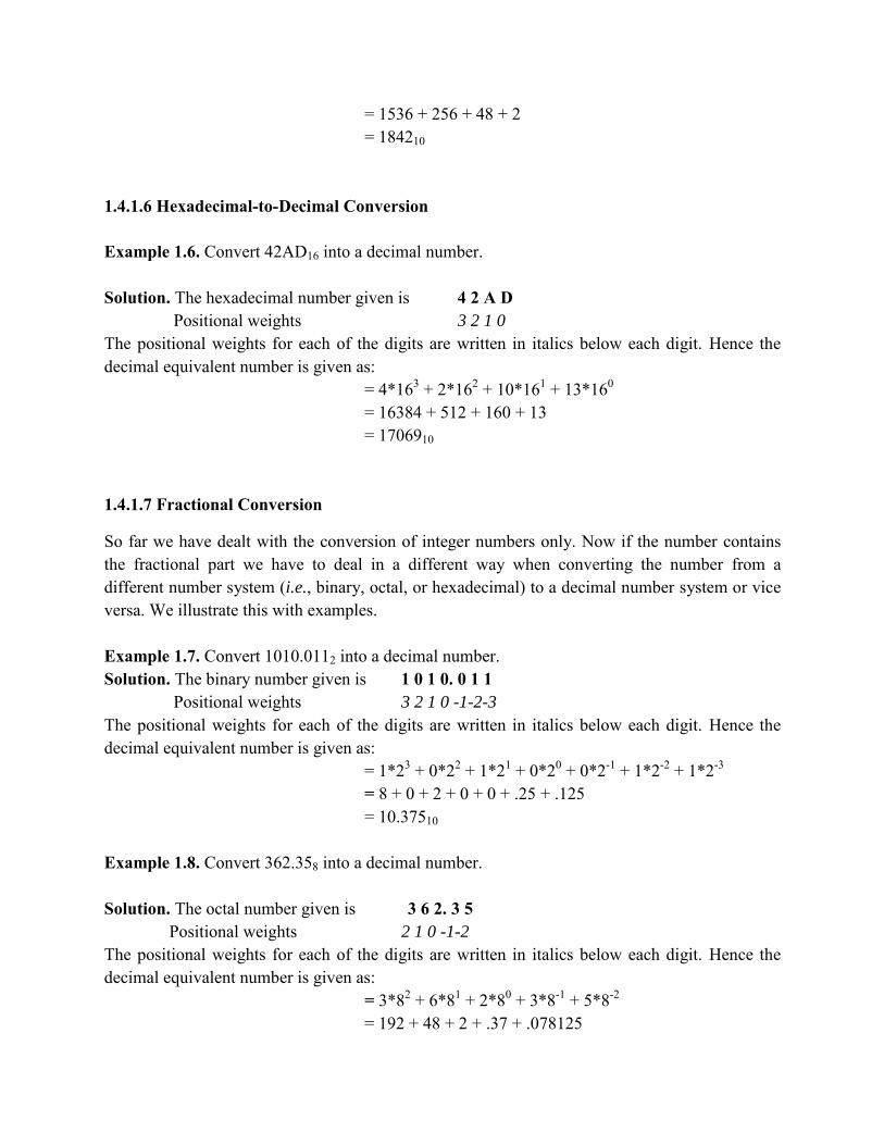
= 242.45212510 Example 1.9. Convert 42A.1216 into a decimal number. Solution. The hexadecimal number given is 4 2 A. 1 2 Positional weights 2 1 0 -1-2
The positional weights for each of the digits are written in italics below each digit. Hence the decimal equivalent number is given as: = 4*162 + 2*161 + 10*160 + 1*16-1 + 2*16-2 = 1024 + 32 + 10 + .0625 + .00393625 = 1066.06640621510 Example 1.10. Convert 25.62510 into a binary number. Solution. Division Quotient Generated remainder 25/2 12 1 12/2 6 0 6/2 3 0 3/2 1 1 1/2 0 1 Therefore, (25)10 = (11001)2 Fractional Part .625 * 2 = 1.250 1 .250 * 2 = .500 0 .500 * 2 = 1.000 1 i.e., (0.625)10 = (0.101)2 Therefore, (25.625)10 = (11001.101)2
Example 1.11. Convert 34.52510 into an octal number. Solution. Division Quotient Generated remainder 34/8 4 2 4/8 0 4 Therefore, (34)10 = (42)8 Fractional Part
.525 * 8 = 4.200 4 .200 * 8 = 1.600 1
.600 * 8 = 4.800 4 i.e., (0.525)10 = (0.414)8 Therefore, (34.525)10 = (42.411)8 Example 1.12. Convert 92.8510 into a hexadecimal number. Solution. Division Quotient Generated remainder 92/16 5 12 5/16 0 5 Therefore, (92)10 = (5C)16 Fractional Part
.85 * 16 = 13.60 13 .60 * 16 = 9.60 9 i.e., (0.85)10 = (0.D9)16 Therefore, (92.85)10 = (5C.D9)16 1.4.1.8 Conversion from a Binary to Octal Number and Vice Versa We know that the maximum digit in an octal number system is 7, which can be represented as 1112 in a binary system. Hence, starting from the LSB, we group three digits at a time and replace them by the decimal equivalent of those groups and we get the final octal number. Example 1.13. Convert 1011010102 into an equivalent octal number. Solution. The binary number given is 101101010 Starting with LSB and grouping 3 bits 101 101 010 Octal equivalent 5 5 2 Hence the octal equivalent number is (552)8. Example 1.14. Convert 10111102 into an equivalent octal number. Solution. The binary number given is 1011110 Starting with LSB and grouping 3 bits 001 011 110 Octal equivalent 1 3 6 Hence the octal equivalent number is (176)8. Since at the time of grouping the three digits in Example 1.14 starting from the LSB, we find that the third group cannot be completed, since only one 1 is left out in the third group, so we
complete the group by adding two 0s in the MSB side. This is called left padding of the number with 0. Now if the number has a fractional part then there will be two different classes of groups—one for the integer part starting from the left of the decimal point and proceeding toward the left and the second one starting from the right of the decimal point and proceeding toward the right. If, for the second class, any 1 is left out, we complete the group by adding two 0s on the right side. This is called right-padding. Example 1.15. Convert 1101.01112 into an equivalent octal number. Solution. The binary number given is 1101.0111 Grouping 3 bits 001 101. 011 100 Octal equivalent: 1 5 3 4 Hence the octal number is (15.34)8.
Now if the octal number is given and you're asked to convert it into its binary equivalent, then each octal digit is converted into a 3-bit-equivalent binary number and—combining all those digits we get the final binary equivalent.
Example 1.16. Convert 2358 into an equivalent binary number. Solution. The octal number given is 2 3 5 3-bit binary equivalent 010 011 101 Hence the binary number is (010011101)2. Example 1.17. Convert 47.3218 into an equivalent binary number. Solution. The octal number given is 4 7 3 2 1 3-bit binary equivalent 100 111 011 010 001 Hence the binary number is (100111.011010001)2. 1.4.1.9 Conversion from a Binary to Hexadecimal Number and Vice Versa We know that the maximum digit in a hexadecimal system is 15, which can be represented by 11112 in a binary system. Hence, starting from the LSB, we group four digits at a time and replace them with the hexadecimal equivalent of those groups and we get the final hexadecimal number.
Example 1.18. Convert 110101102 into an equivalent hexadecimal number. Solution. The binary number given is 11010110 Starting with LSB and grouping 4 bits 1101 0110 Hexadecimal equivalent D 6 Hence the hexadecimal equivalent number is (D6)16. Example 1.19. Convert 1100111102 into an equivalent hexadecimal number. Solution. The binary number given is 110011110 Starting with LSB and grouping 4 bits 0001 1001 1110 Hexadecimal equivalent 1 9 E Hence the hexadecimal equivalent number is (19E)16.
Since at the time of grouping of four digits starting from the LSB, in Example 1.19 we find that the third group cannot be completed, since only one 1 is left out, so we complete the group by adding three 0s to the MSB side. Now if the number has a fractional part, as in the case of octal numbers, then there will be two different classes of groups—one for the integer part starting from the left of the decimal point and proceeding toward the left and the second one starting from the right of the decimal point and proceeding toward the right. If, for the second class, any uncompleted group is left out, we complete the group by adding 0s on the right side. Example 1.20. Convert 111011.0112 into an equivalent hexadecimal number. Solution. The binary number given is 111011.011 Grouping 4 bits 0011 1011. 0110 Hexadecimal equivalent 3 B 6 Hence the hexadecimal equivalent number is (3B.6)16.
Now if the hexadecimal number is given and you're asked to convert it into its binary equivalent, then each hexadecimal digit is converted into a 4-bit-equivalent binary number and by combining all those digits we get the final binary equivalent.
Example 1.21. Convert 29C16 into an equivalent binary number. Solution. The hexadecimal number given is 2 9 C 4-bit binary equivalent 0010 1001 1100 Hence the equivalent binary number is (001010011100)2.
Example 1.22. Convert 9E.AF216 into an equivalent binary number. Solution. The hexadecimal number given is 9 E.A F 2 4-bit binary equivalent 1001 1110 1010 1111 0010 Hence the equivalent binary number is (10011110.101011110010)2. 1.4.1.10 Conversion from an Octal to Hexadecimal Number and Vice Versa Conversion from octal to hexadecimal and vice versa is sometimes required. To convert an octal number into a hexadecimal number the following steps are to be followed:
i. First convert the octal number to its binary equivalent (as already discussed above). ii. Then form groups of 4 bits, starting from the LSB.
iii. Then write the equivalent hexadecimal number for each group of 4 bits. Similarly, for converting a hexadecimal number into an octal number the following steps are to be followed:
i. First convert the hexadecimal number to its binary equivalent. ii. Then form groups of 3 bits, starting from the LSB.
iii. Then write the equivalent octal number for each group of 3 bits. Example 1.23. Convert the following hexadecimal numbers into equivalent octal numbers. (a) A72E (b) 4.BF85 Solution. (a) Given hexadecimal number is A 7 2 E Binary equivalent is 1010 0111 0010 1110 = 1010011100101110 Forming groups of 3 bits from the LSB 001 010 011 100 101 110 Octal equivalent 1 2 3 4 5 6 Hence the octal equivalent of (A72E)16 is (123456)8. (b) Given hexadecimal number is 4 B F 8 5 Binary equivalent is 0100 1011 1111 1000 0101 = 0100.1011111110000101 Forming groups of 3 bits 100. 101 111 111 000 010 100 Octal equivalent 4 5 7 7 0 2 4 Hence the octal equivalent of (4.BF85)16 is (4.577024)8.
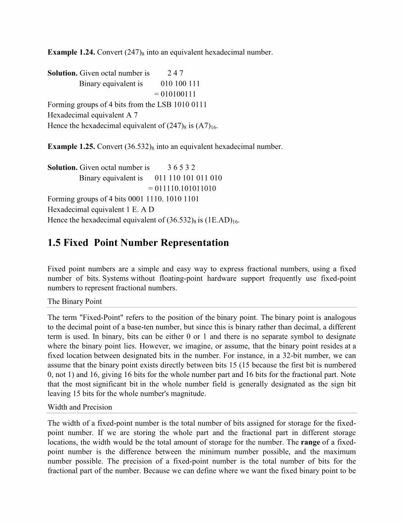
Example 1.24. Convert (247)8 into an equivalent hexadecimal number. Solution. Given octal number is 2 4 7 Binary equivalent is 010 100 111 = 010100111 Forming groups of 4 bits from the LSB 1010 0111 Hexadecimal equivalent A 7 Hence the hexadecimal equivalent of (247)8 is (A7)16. Example 1.25. Convert (36.532)8 into an equivalent hexadecimal number. Solution. Given octal number is 3 6 5 3 2 Binary equivalent is 011 110 101 011 010 = 011110.101011010 Forming groups of 4 bits 0001 1110. 1010 1101 Hexadecimal equivalent 1 E. A D Hence the hexadecimal equivalent of (36.532)8 is (1E.AD)16.
1.5 Fixed Point Number Representation
Fixed point numbers are a simple and easy way to express fractional numbers, using a fixed number of bits. Systems without floating-point hardware support frequently use fixed-point numbers to represent fractional numbers.
The Binary Point
The term "Fixed-Point" refers to the position of the binary point. The binary point is analogous to the decimal point of a base-ten number, but since this is binary rather than decimal, a different term is used. In binary, bits can be either 0 or 1 and there is no separate symbol to designate where the binary point lies. However, we imagine, or assume, that the binary point resides at a fixed location between designated bits in the number. For instance, in a 32-bit number, we can assume that the binary point exists directly between bits 15 (15 because the first bit is numbered 0, not 1) and 16, giving 16 bits for the whole number part and 16 bits for the fractional part. Note that the most significant bit in the whole number field is generally designated as the sign bit leaving 15 bits for the whole number's magnitude.
Width and Precision
The width of a fixed-point number is the total number of bits assigned for storage for the fixed-point number. If we are storing the whole part and the fractional part in different storage locations, the width would be the total amount of storage for the number. The range of a fixed-point number is the difference between the minimum number possible, and the maximum number possible. The precision of a fixed-point number is the total number of bits for the fractional part of the number. Because we can define where we want the fixed binary point to be
located, the precision can be any number up to and including the width of the number. Note however, that the more precision we have, the less total range we have.
There are a number of standards, but in this book we will use n for the width of a fixed-point number, p for the precision, and R for the total range.
Examples
Not all numbers can be represented exactly by a fixed-point number, and so the closest approximation is used.
The formula for calculating the integer representation (X) in a Qm.n format of a float number (x) is:
X = round( x*2n )
To convert it back the following formula is used:
x = X * 2-n
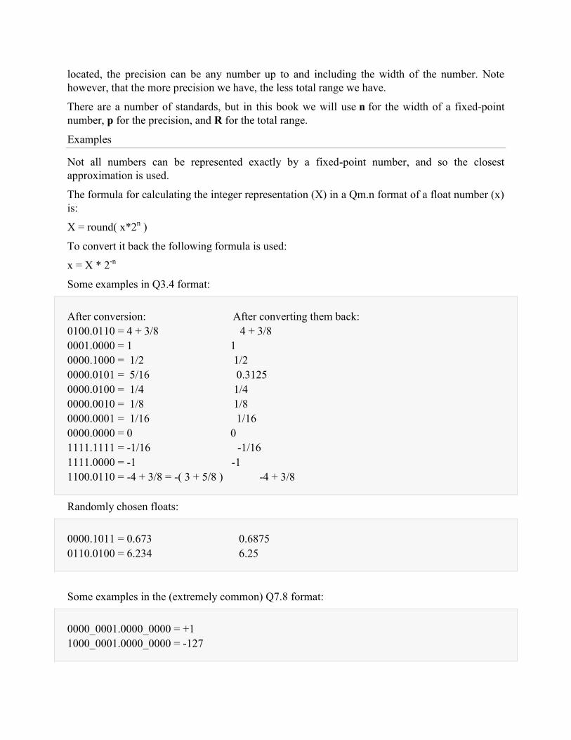
Some examples in Q3.4 format:
After conversion: After converting them back: 0100.0110 = 4 + 3/8 4 + 3/8 0001.0000 = 1 1 0000.1000 = 1/2 1/2 0000.0101 = 5/16 0.3125 0000.0100 = 1/4 1/4 0000.0010 = 1/8 1/8 0000.0001 = 1/16 1/16 0000.0000 = 0 0 1111.1111 = -1/16 -1/16 1111.0000 = -1 -1 1100.0110 = -4 + 3/8 = -( 3 + 5/8 ) -4 + 3/8
Randomly chosen floats:
0000.1011 = 0.673 0.6875 0110.0100 = 6.234 6.25
Some examples in the (extremely common) Q7.8 format:
0000_0001.0000_0000 = +1 1000_0001.0000_0000 = -127
0000_0000.0100_0000 = 1/4
Arithmetic
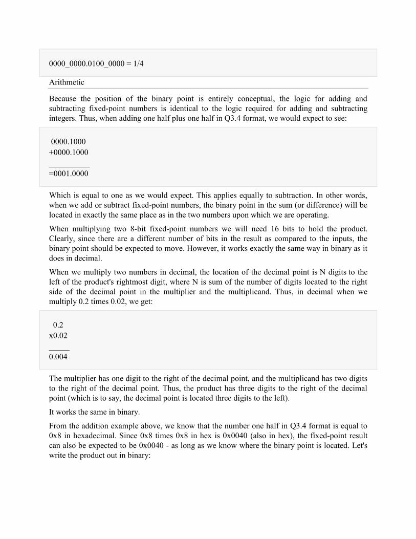
Because the position of the binary point is entirely conceptual, the logic for adding and subtracting fixed-point numbers is identical to the logic required for adding and subtracting integers. Thus, when adding one half plus one half in Q3.4 format, we would expect to see:
0000.1000 +0000.1000 __________ =0001.0000
Which is equal to one as we would expect. This applies equally to subtraction. In other words, when we add or subtract fixed-point numbers, the binary point in the sum (or difference) will be located in exactly the same place as in the two numbers upon which we are operating.
When multiplying two 8-bit fixed-point numbers we will need 16 bits to hold the product. Clearly, since there are a different number of bits in the result as compared to the inputs, the binary point should be expected to move. However, it works exactly the same way in binary as it does in decimal.
When we multiply two numbers in decimal, the location of the decimal point is N digits to the left of the product's rightmost digit, where N is sum of the number of digits located to the right side of the decimal point in the multiplier and the multiplicand. Thus, in decimal when we multiply 0.2 times 0.02, we get:
0.2 x0.02 _____ 0.004
The multiplier has one digit to the right of the decimal point, and the multiplicand has two digits to the right of the decimal point. Thus, the product has three digits to the right of the decimal point (which is to say, the decimal point is located three digits to the left).
It works the same in binary.
From the addition example above, we know that the number one half in Q3.4 format is equal to 0x8 in hexadecimal. Since 0x8 times 0x8 in hex is 0x0040 (also in hex), the fixed-point result can also be expected to be 0x0040 - as long as we know where the binary point is located. Let's write the product out in binary:
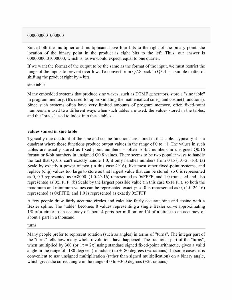
0000000001000000
Since both the multiplier and multiplicand have four bits to the right of the binary point, the location of the binary point in the product is eight bits to the left. Thus, our answer is 00000000.01000000, which is, as we would expect, equal to one quarter.
If we want the format of the output to be the same as the format of the input, we must restrict the range of the inputs to prevent overflow. To convert from Q7.8 back to Q3.4 is a simple matter of shifting the product right by 4 bits.
sine table
Many embedded systems that produce sine waves, such as DTMF generators, store a "sine table" in program memory. (It's used for approximating the mathematical sine() and cosine() functions). Since such systems often have very limited amounts of program memory, often fixed-point numbers are used two different ways when such tables are used: the values stored in the tables, and the "brads" used to index into these tables.
values stored in sine table Typically one quadrant of the sine and cosine functions are stored in that table. Typically it is a quadrant where those functions produce output values in the range of 0 to +1. The values in such tables are usually stored as fixed point numbers -- often 16-bit numbers in unsigned Q0.16 format or 8-bit numbers in unsigned Q0.8 values. There seems to be two popular ways to handle the fact that Q0.16 can't exactly handle 1.0, it only handles numbers from 0 to (1.0-2^-16): (a) Scale by exactly a power of two (in this case 2^16), like most other fixed-point systems, and replace (clip) values too large to store as that largest value that can be stored: so 0 is represented as 0, 0.5 represented as 0x8000, (1.0-2^-16) represented as 0xFFFF, and 1.0 truncated and also represented as 0xFFFF. (b) Scale by the largest possible value (in this case 0xFFFF), so both the maximum and minimum values can be represented exactly: so 0 is represented as 0, (1.0-2^-16) represented as 0xFFFE, and 1.0 is represented as exactly 0xFFFF
A few people draw fairly accurate circles and calculate fairly accurate sine and cosine with a Bezier spline. The "table" becomes 8 values representing a single Bezier curve approximating 1/8 of a circle to an accuracy of about 4 parts per million, or 1/4 of a circle to an accuracy of about 1 part in a thousand.
turns
Many people prefer to represent rotation (such as angles) in terms of "turns". The integer part of the "turns" tells how many whole revolutions have happened. The fractional part of the "turns", when multiplied by 360 (or 1τ = 2π) using standard signed fixed-point arithmetic, gives a valid angle in the range of -180 degrees (-π radians) to +180 degrees (+π radians). In some cases, it is
convenient to use unsigned multiplication (rather than signed multiplication) on a binary angle, which gives the correct angle in the range of 0 to +360 degrees (+2π radians).
The main advantage to storing angles as a fixed-point fraction of a turn is speed. Combining some "current position" angle with some positive or negative "incremental angle" to get the "new position" is very fast, even on slow 8-bit microcontrollers: it takes a single "integer addition", ignoring overflow. Other formats for storing angles require the same addition, plus special cases to handle the edge cases of overflowing 360 degrees or underflowing 0 degrees.
Compared to storing angles in a binary angle format, storing angles in any other format -- such as 360 degrees to give one complete revolution, or 2π radians to give one complete revolution -- inevitably results in some bit patterns giving "angles" outside that range, requiring extra steps to range-reduce the value to the desired range, or results in some bit patterns that are not valid angles at all (NaN), or both.
Using a binary angle format in units of "turns" allows us to quickly (using shift-and-mask, avoiding multiply) separate the bits into:
bits that represent integer turns (ignored when looking up the sine of the angle; some systems never bother storing these bits in the first place)
2 bits that represent the quadrant bits that are directly used to index into the lookup table low-order bits less than one "step" into the index table (phase accumulator bits, ignored
when looking up the sine of the angle without interpolation) The low-order phase bits give improved frequency resolution, even without interpolation.
Some systems use the low-order bits to linearly interpolate between values in the table. This allows you to get more accuracy using a smaller table (saving program space), by sacrificing a few cycles on this "extra" interpolation calculation. A few systems get even more accuracy using an even smaller table by sacrificing a few more cycles to use those low-order bits to calculate cubic interpolation.
Perhaps the most common binary angle format is "brads".
brads Many embedded systems store the angle, the fractional part of the "turns", in a single byte binary angle format. There are several ways of interpreting the value in that byte, all of which mean (more or less) the same angle:
an angle in units of brads (binary radians) stored as an 8 bit unsigned integer, from 0 to 255 brads
an angle in units of brads stored as an 8 bit signed integer, from -128 to +127 brads an angle in units of "turns", stored as a fractional turn in unsigned Q0.8 format, from 0 to
just under 1 full turn an angle in units of "turns", stored as a fractional turn in signed Q0.7 (?) format, from -
1/2 to just under +1/2 full turn One full turn is 256 brads is 360 degrees.
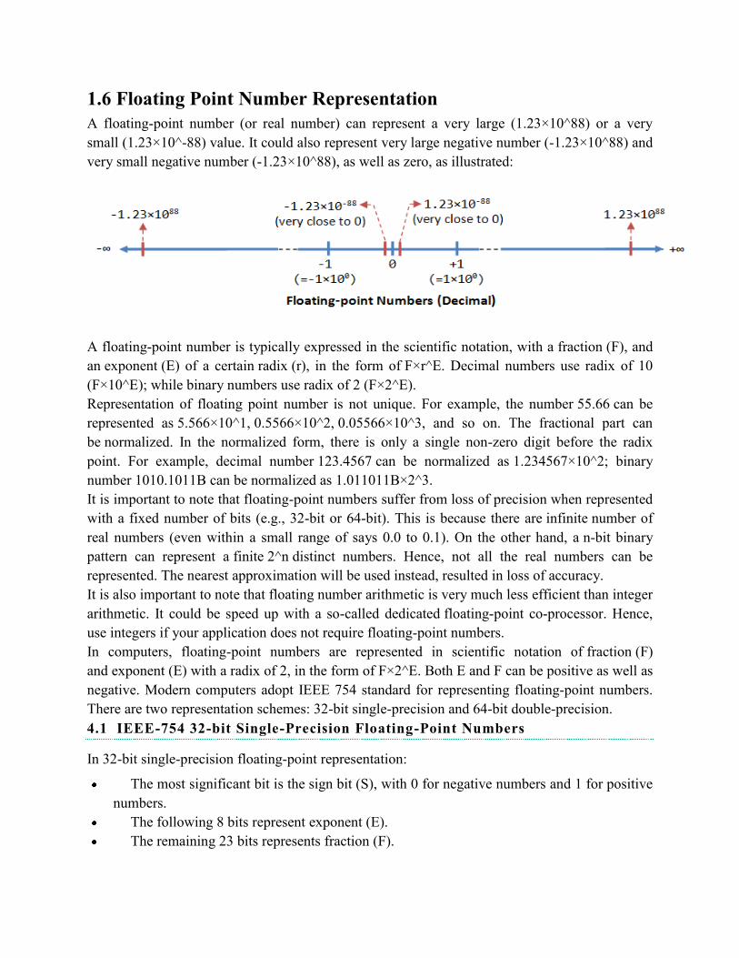
1.6 Floating Point Number Representation A floating-point number (or real number) can represent a very large (1.23×10^88) or a very small (1.23×10^-88) value. It could also represent very large negative number (-1.23×10^88) and very small negative number (-1.23×10^88), as well as zero, as illustrated:
A floating-point number is typically expressed in the scientific notation, with a fraction (F), and an exponent (E) of a certain radix (r), in the form of F×r^E. Decimal numbers use radix of 10 (F×10^E); while binary numbers use radix of 2 (F×2^E). Representation of floating point number is not unique. For example, the number 55.66 can be represented as 5.566×10^1, 0.5566×10^2, 0.05566×10^3, and so on. The fractional part can be normalized. In the normalized form, there is only a single non-zero digit before the radix point. For example, decimal number 123.4567 can be normalized as 1.234567×10^2; binary number 1010.1011B can be normalized as 1.011011B×2^3. It is important to note that floating-point numbers suffer from loss of precision when represented with a fixed number of bits (e.g., 32-bit or 64-bit). This is because there are infinite number of real numbers (even within a small range of says 0.0 to 0.1). On the other hand, a n-bit binary pattern can represent a finite 2^n distinct numbers. Hence, not all the real numbers can be represented. The nearest approximation will be used instead, resulted in loss of accuracy. It is also important to note that floating number arithmetic is very much less efficient than integer arithmetic. It could be speed up with a so-called dedicated floating-point co-processor. Hence, use integers if your application does not require floating-point numbers. In computers, floating-point numbers are represented in scientific notation of fraction (F) and exponent (E) with a radix of 2, in the form of F×2^E. Both E and F can be positive as well as negative. Modern computers adopt IEEE 754 standard for representing floating-point numbers. There are two representation schemes: 32-bit single-precision and 64-bit double-precision. 4.1 IEEE-754 32-bit Single-Precision Floating-Point Numbers
In 32-bit single-precision floating-point representation:
The most significant bit is the sign bit (S), with 0 for negative numbers and 1 for positive numbers.
The following 8 bits represent exponent (E). The remaining 23 bits represents fraction (F).
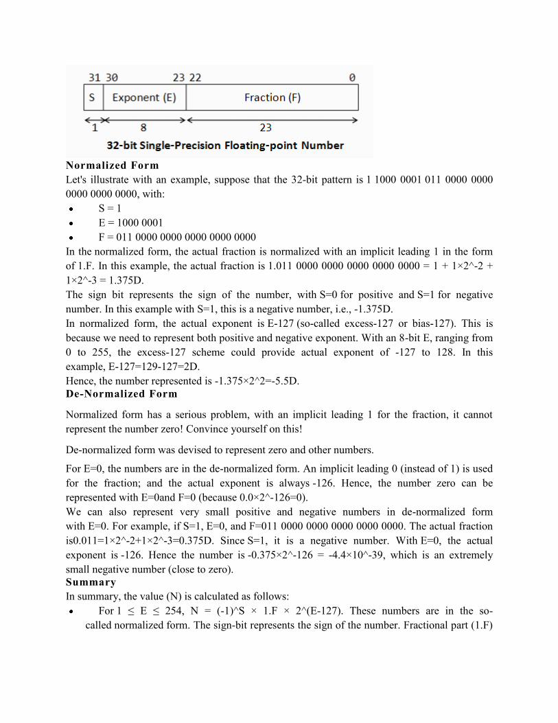
Normalized Form Let's illustrate with an example, suppose that the 32-bit pattern is 1 1000 0001 011 0000 0000 0000 0000 0000, with:
S = 1 E = 1000 0001 F = 011 0000 0000 0000 0000 0000
In the normalized form, the actual fraction is normalized with an implicit leading 1 in the form of 1.F. In this example, the actual fraction is 1.011 0000 0000 0000 0000 0000 = 1 + 1×2^-2 + 1×2^-3 = 1.375D. The sign bit represents the sign of the number, with S=0 for positive and S=1 for negative number. In this example with S=1, this is a negative number, i.e., -1.375D. In normalized form, the actual exponent is E-127 (so-called excess-127 or bias-127). This is because we need to represent both positive and negative exponent. With an 8-bit E, ranging from 0 to 255, the excess-127 scheme could provide actual exponent of -127 to 128. In this example, E-127=129-127=2D. Hence, the number represented is -1.375×2^2=-5.5D. De-Normalized Form
Normalized form has a serious problem, with an implicit leading 1 for the fraction, it cannot represent the number zero! Convince yourself on this!
De-normalized form was devised to represent zero and other numbers.
For E=0, the numbers are in the de-normalized form. An implicit leading 0 (instead of 1) is used for the fraction; and the actual exponent is always -126. Hence, the number zero can be represented with E=0and F=0 (because 0.0×2^-126=0). We can also represent very small positive and negative numbers in de-normalized form with E=0. For example, if S=1, E=0, and F=011 0000 0000 0000 0000 0000. The actual fraction is0.011=1×2^-2+1×2^-3=0.375D. Since S=1, it is a negative number. With E=0, the actual exponent is -126. Hence the number is -0.375×2^-126 = -4.4×10^-39, which is an extremely small negative number (close to zero). Summary In summary, the value (N) is calculated as follows:
For 1 ≤ E ≤ 254, N = (-1)^S × 1.F × 2^(E-127). These numbers are in the so-called normalized form. The sign-bit represents the sign of the number. Fractional part (1.F)
are normalized with an implicit leading 1. The exponent is bias (or in excess) of 127, so as to represent both positive and negative exponent. The range of exponent is -126 to +127.
For E = 0, N = (-1)^S × 0.F × 2^(-126). These numbers are in the so-called denormalized form. The exponent of 2^-126 evaluates to a very small number. Denormalized form is needed to represent zero (with F=0 and E=0). It can also represents very small positive and negative number close to zero.
For E = 255, it represents special values, such as ±INF (positive and negative infinity) and NaN (not a number). This is beyond the scope of this article.
Example 1: Suppose that IEEE-754 32-bit floating-point representation pattern is 0 10000000 110 0000 0000 0000 0000 0000.
Sign bit S = 0 ⇒ positive number
E = 1000 0000B = 128D (in normalized form)
Fraction is 1.11B (with an implicit leading 1) = 1 + 1×2^-1 + 1×2^-2 = 1.75D
The number is +1.75 × 2^(128-127) = +3.5D
Example 2: Suppose that IEEE-754 32-bit floating-point representation pattern is 1 01111110 100 0000 0000 0000 0000 0000.
Sign bit S = 1 ⇒ negative number E = 0111 1110B = 126D (in normalized form)
Fraction is 1.1B (with an implicit leading 1) = 1 + 2^-1 = 1.5D
The number is -1.5 × 2^(126-127) = -0.75D
Example 3: Suppose that IEEE-754 32-bit floating-point representation pattern is 1 01111110 000 0000 0000 0000 0000 0001.
Sign bit S = 1 ⇒ negative number E = 0111 1110B = 126D (in normalized form)
Fraction is 1.000 0000 0000 0000 0000 0001B (with an implicit leading 1) = 1 + 2^-23
The number is -(1 + 2^-23) × 2^(126-127) = -0.500000059604644775390625 (may not be exact in decimal!)
Example 4 (De-Normalized Form): Suppose that IEEE-754 32-bit floating-point representation pattern is 1 00000000 000 0000 0000 0000 0000 0001.
Sign bit S = 1 ⇒ negative number
E = 0 (in de-normalized form)
Fraction is 0.000 0000 0000 0000 0000 0001B (with an implicit leading 0) = 1×2^-23
The number is -2^-23 × 2^(-126) = -2×(-149) ≈ -1.4×10^-45
4.2 Exercises (Floating-point Numbers)
1. Compute the largest and smallest positive numbers that can be represented in the 32-bit normalized form.
2. Compute the largest and smallest negative numbers can be represented in the 32-bit normalized form.
3. Repeat (1) for the 32-bit de-normalized form.
4. Repeat (2) for the 32-bit de-normalized form. Hints:
1. Largest positive number: S=0, E=1111 1110 (254), F=111 1111 1111 1111 1111 1111. Smallest positive number: S=0, E=0000 00001 (1), F=000 0000 0000 0000 0000 0000.
2. Same as above, but S=1. 3. Largest positive number: S=0, E=0, F=111 1111 1111 1111 1111 1111.
Smallest positive number: S=0, E=0, F=000 0000 0000 0000 0000 0001. 4. Same as above, but S=1.
Notes For Java Users You can use JDK methods Float.intBitsToFloat(int bits) or Double.longBitsToDouble(long bits) to create a single-precision 32-bit float or double-precision 64-bit double with the specific bit patterns, and print their values. For examples,
System.out.println(Float.intBitsToFloat(0x7fffff));
System.out.println(Double.longBitsToDouble(0x1fffffffffffffL));
4.3 IEEE-754 64-bit Double-Precision Floating-Point Numbers
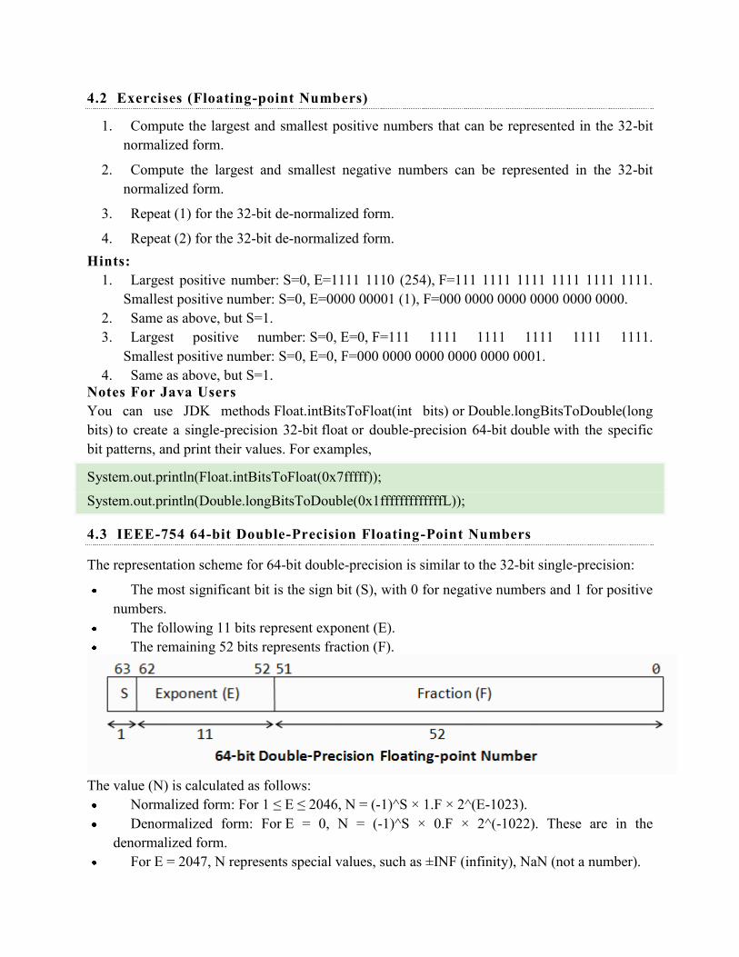
The representation scheme for 64-bit double-precision is similar to the 32-bit single-precision:
The most significant bit is the sign bit (S), with 0 for negative numbers and 1 for positive numbers.
The following 11 bits represent exponent (E). The remaining 52 bits represents fraction (F).
The value (N) is calculated as follows:
Normalized form: For 1 ≤ E ≤ 2046, N = (-1)^S × 1.F × 2^(E-1023). Denormalized form: For E = 0, N = (-1)^S × 0.F × 2^(-1022). These are in the
denormalized form. For E = 2047, N represents special values, such as ±INF (infinity), NaN (not a number).
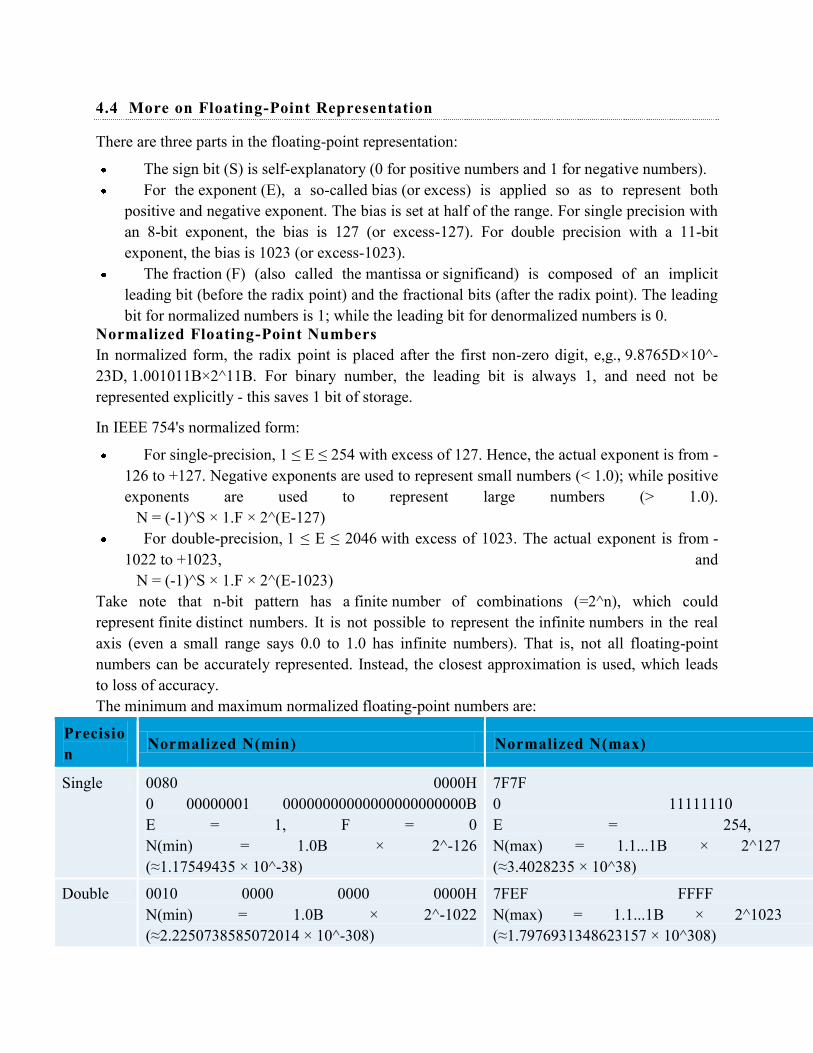
4.4 More on Floating-Point Representation
There are three parts in the floating-point representation:
The sign bit (S) is self-explanatory (0 for positive numbers and 1 for negative numbers). For the exponent (E), a so-called bias (or excess) is applied so as to represent both
positive and negative exponent. The bias is set at half of the range. For single precision with an 8-bit exponent, the bias is 127 (or excess-127). For double precision with a 11-bit exponent, the bias is 1023 (or excess-1023).
The fraction (F) (also called the mantissa or significand) is composed of an implicit leading bit (before the radix point) and the fractional bits (after the radix point). The leading bit for normalized numbers is 1; while the leading bit for denormalized numbers is 0.
Normalized Floating-Point Numbers In normalized form, the radix point is placed after the first non-zero digit, e,g., 9.8765D×10^-23D, 1.001011B×2^11B. For binary number, the leading bit is always 1, and need not be represented explicitly - this saves 1 bit of storage.
In IEEE 754's normalized form:
For single-precision, 1 ≤ E ≤ 254 with excess of 127. Hence, the actual exponent is from -126 to +127. Negative exponents are used to represent small numbers (< 1.0); while positive exponents are used to represent large numbers (> 1.0). N = (-1)^S × 1.F × 2^(E-127)
For double-precision, 1 ≤ E ≤ 2046 with excess of 1023. The actual exponent is from -1022 to +1023, and N = (-1)^S × 1.F × 2^(E-1023)
Take note that n-bit pattern has a finite number of combinations (=2^n), which could represent finite distinct numbers. It is not possible to represent the infinite numbers in the real axis (even a small range says 0.0 to 1.0 has infinite numbers). That is, not all floating-point numbers can be accurately represented. Instead, the closest approximation is used, which leads to loss of accuracy. The minimum and maximum normalized floating-point numbers are:
Precision Normalized N(min) Normalized N(max)
Single 0080 0000H 0 00000001 00000000000000000000000B E = 1, F = 0 N(min) = 1.0B × 2^-126 (≈1.17549435 × 10^-38)
7F7F FFFFH 0 11111110 00000000000000000000000B E = 254, F = 0 N(max) = 1.1...1B × 2^127 = (2 - 2^-23) × 2^127 (≈3.4028235 × 10^38)
Double 0010 0000 0000 0000H N(min) = 1.0B × 2^-1022 (≈2.2250738585072014 × 10^-308)
7FEF FFFF FFFF FFFFH N(max) = 1.1...1B × 2^1023 = (2 - 2^-52) × 2^1023 (≈1.7976931348623157 × 10^308)
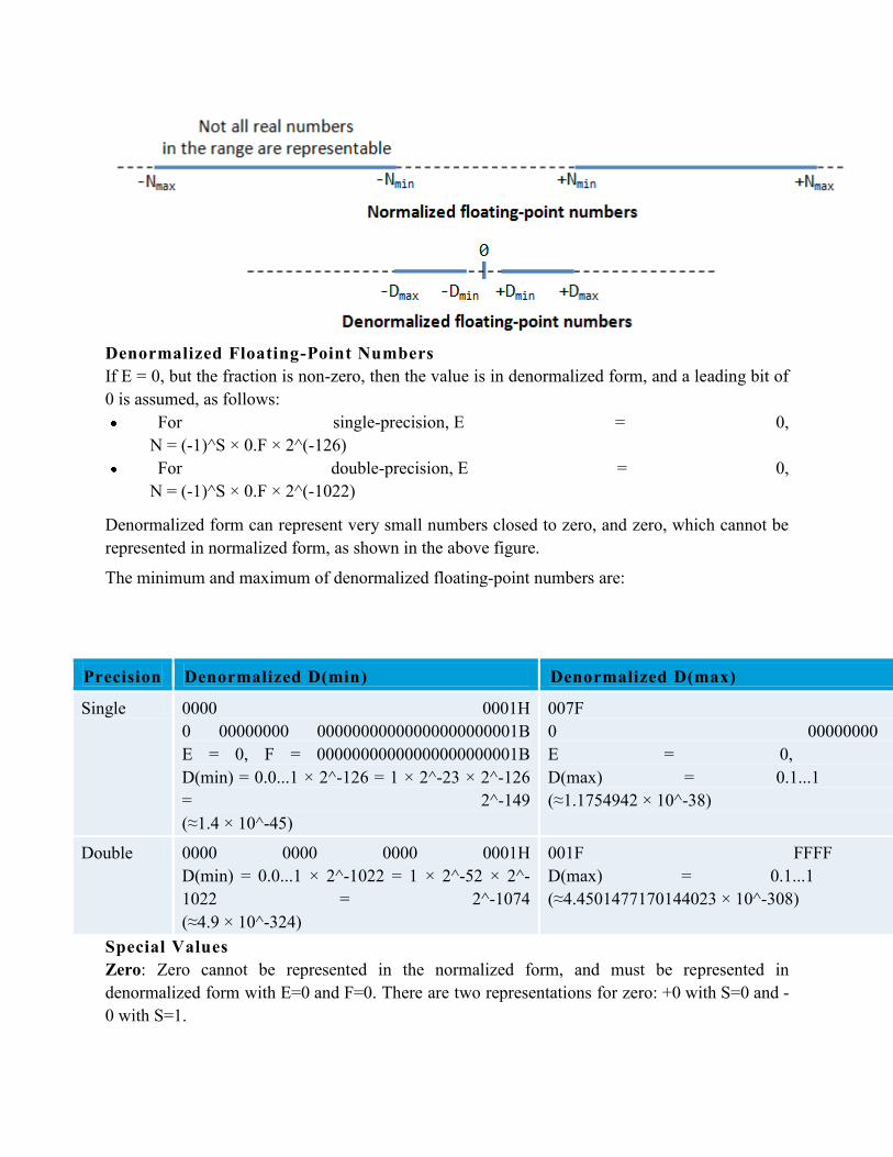
Denormalized Floating-Point Numbers If E = 0, but the fraction is non-zero, then the value is in denormalized form, and a leading bit of 0 is assumed, as follows:
For single-precision, E = 0, N = (-1)^S × 0.F × 2^(-126)
For double-precision, E = 0, N = (-1)^S × 0.F × 2^(-1022)
Denormalized form can represent very small numbers closed to zero, and zero, which cannot be represented in normalized form, as shown in the above figure.
The minimum and maximum of denormalized floating-point numbers are:
Precision Denormalized D(min) Denormalized D(max)
Single 0000 0001H 0 00000000 00000000000000000000001B E = 0, F = 00000000000000000000001B D(min) = 0.0...1 × 2^-126 = 1 × 2^-23 × 2^-126 = 2^-149 (≈1.4 × 10^-45)
007F FFFFH 0 00000000 11111111111111111111111B E = 0, F = 11111111111111111111111B D(max) = 0.1...1 × 2^-126 = (1-2^-23)×2^-126 (≈1.1754942 × 10^-38)
Double 0000 0000 0000 0001H D(min) = 0.0...1 × 2^-1022 = 1 × 2^-52 × 2^-1022 = 2^-1074 (≈4.9 × 10^-324)
001F FFFF FFFF FFFFH D(max) = 0.1...1 × 2^-1022 = (1-2^-52)×2^-1022 (≈4.4501477170144023 × 10^-308)
Special Values Zero: Zero cannot be represented in the normalized form, and must be represented in denormalized form with E=0 and F=0. There are two representations for zero: +0 with S=0 and -0 with S=1.
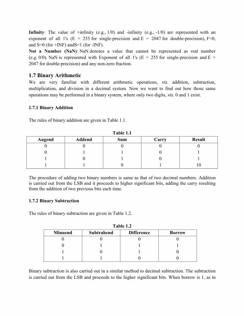
Infinity: The value of +infinity (e.g., 1/0) and -infinity (e.g., -1/0) are represented with an exponent of all 1's (E = 255 for single-precision and E = 2047 for double-precision), F=0, and S=0 (for +INF) andS=1 (for -INF). Not a Number (NaN): NaN denotes a value that cannot be represented as real number (e.g. 0/0). NaN is represented with Exponent of all 1's (E = 255 for single-precision and E = 2047 for double-precision) and any non-zero fraction.
1.7 Binary Arithmetic We are very familiar with different arithmetic operations, viz. addition, subtraction, multiplication, and division in a decimal system. Now we want to find out how those same operations may be performed in a binary system, where only two digits, viz. 0 and 1 exist. 1.7.1 Binary Addition The rules of binary addition are given in Table 1.1.
Table 1.1
Augend Addend Sum Carry Result 0 0 1 1
0 1 0 1
0 1 1 0
0 0 0 1
0 1 1 10
The procedure of adding two binary numbers is same as that of two decimal numbers. Addition is carried out from the LSB and it proceeds to higher significant bits, adding the carry resulting from the addition of two previous bits each time. 1.7.2 Binary Subtraction The rules of binary subtraction are given in Table 1.2.
Table 1.2 Minuend Subtrahend Difference Borrow
0 0 1 1
0 1 0 1
0 1 1 0
0 1 0 0
Binary subtraction is also carried out in a similar method to decimal subtraction. The subtraction is carried out from the LSB and proceeds to the higher significant bits. When borrow is 1, as in
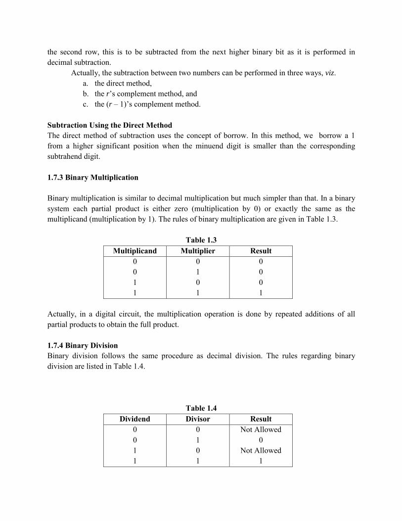
the second row, this is to be subtracted from the next higher binary bit as it is performed in decimal subtraction.
Actually, the subtraction between two numbers can be performed in three ways, viz. a. the direct method, b. the r‘s complement method, and c. the (r – 1)‘s complement method.
Subtraction Using the Direct Method The direct method of subtraction uses the concept of borrow. In this method, we borrow a 1 from a higher significant position when the minuend digit is smaller than the corresponding subtrahend digit. 1.7.3 Binary Multiplication Binary multiplication is similar to decimal multiplication but much simpler than that. In a binary system each partial product is either zero (multiplication by 0) or exactly the same as the multiplicand (multiplication by 1). The rules of binary multiplication are given in Table 1.3.
Table 1.3 Multiplicand Multiplier Result
0 0 1 1
0 1 0 1
0 0 0 1
Actually, in a digital circuit, the multiplication operation is done by repeated additions of all partial products to obtain the full product. 1.7.4 Binary Division Binary division follows the same procedure as decimal division. The rules regarding binary division are listed in Table 1.4.
Table 1.4 Dividend Divisor Result
0 0 1 1
0 1 0 1
Not Allowed 0
Not Allowed 1
At their lowest level, computers cannot subtract, multiply, or divide. Neither can calculators. The world's largest and fastest supercomputer can only add—that's it. It performs the addition at the bit level. Binary arithmetic is the only means by which any electronic digital computing machine can perform arithmetic.
Suppose you want the computer to add seven 6s together. If you asked the computer (through programming) to perform the calculation
6 + 6 + 6 + 6 + 6 + 6 + 6
the computer would zing the answer, 42, back to you before you could say bit bucket. The computer has no problem performing addition. The problems arise when you request that the computer perform another type of calculation, such as this one:
42 – 6 – 6 – 6 – 6 – 6 – 6 – 6
Because the computer can only add, it cannot do the subtraction. However, the computer can negate numbers. That is, the computer can take the negative of a number. Therefore, it can take the negative of 6 and represent (at the bit level) negative 6. Once it has done that, it can add –6 to 42 seven times. In effect, the internal calculation becomes this:
42 + (–6) + (–6) + (–6) + (–6) + (–6) + (–6) + (–6)
Adding seven –6s produces the correct result of 0. This may seem like a cop-out to you. After all, the computer is really subtracting, right? In reality, the computer is not subtracting. At its bit level, the computer can convert a number to its negative through a process known as 2's complement. A number's 2's complement is the negative of its original value at the bit level. The computer has in its internal logic circuits the capability to convert a number to its 2's complement and then carry out the addition of negatives, thereby seemingly performing subtraction.
Once the computer can add and simulate subtraction, it can simulate multiplying and dividing. To multiply 6 times 7, the computer actually adds 6 together seven times and produces 42. Therefore
6 x 7
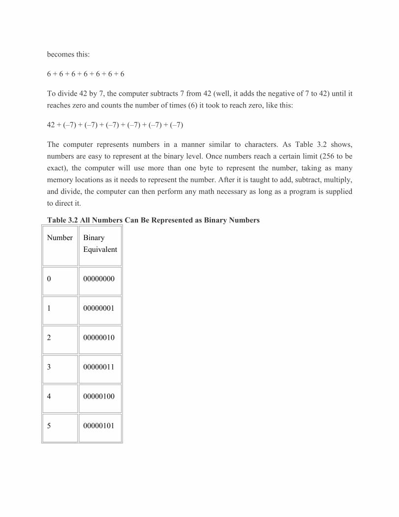
becomes this:
6 + 6 + 6 + 6 + 6 + 6 + 6
To divide 42 by 7, the computer subtracts 7 from 42 (well, it adds the negative of 7 to 42) until it reaches zero and counts the number of times (6) it took to reach zero, like this:
42 + (–7) + (–7) + (–7) + (–7) + (–7) + (–7)
The computer represents numbers in a manner similar to characters. As Table 3.2 shows, numbers are easy to represent at the binary level. Once numbers reach a certain limit (256 to be exact), the computer will use more than one byte to represent the number, taking as many memory locations as it needs to represent the number. After it is taught to add, subtract, multiply, and divide, the computer can then perform any math necessary as long as a program is supplied to direct it.
Table 3.2 All Numbers Can Be Represented as Binary Numbers
Number Binary Equivalent
0 00000000
1 00000001
2 00000010
3 00000011
4 00000100
5 00000101
6 00000110
7 00000111
8 00001000
9 00001001
10 00001010
11 00001011
12 00001100
13 00001101
14 00001110
15 00001111
16 00010000
17 00010001
18 00010010
19 00010011
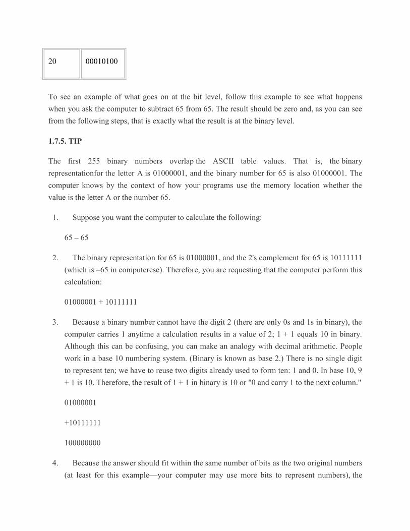
20 00010100
To see an example of what goes on at the bit level, follow this example to see what happens when you ask the computer to subtract 65 from 65. The result should be zero and, as you can see from the following steps, that is exactly what the result is at the binary level.
1.7.5. TIP
The first 255 binary numbers overlap the ASCII table values. That is, the binary representationfor the letter A is 01000001, and the binary number for 65 is also 01000001. The computer knows by the context of how your programs use the memory location whether the value is the letter A or the number 65.
1. Suppose you want the computer to calculate the following:
65 – 65
2. The binary representation for 65 is 01000001, and the 2's complement for 65 is 10111111 (which is –65 in computerese). Therefore, you are requesting that the computer perform this calculation:
01000001 + 10111111
3. Because a binary number cannot have the digit 2 (there are only 0s and 1s in binary), the computer carries 1 anytime a calculation results in a value of 2; 1 + 1 equals 10 in binary. Although this can be confusing, you can make an analogy with decimal arithmetic. People work in a base 10 numbering system. (Binary is known as base 2.) There is no single digit to represent ten; we have to reuse two digits already used to form ten: 1 and 0. In base 10, 9 + 1 is 10. Therefore, the result of 1 + 1 in binary is 10 or "0 and carry 1 to the next column."
01000001
+10111111
100000000
4. Because the answer should fit within the same number of bits as the two original numbers (at least for this example—your computer may use more bits to represent numbers), the
ninth bit is discarded, leaving the zero result. This example shows that binary 65 plus binary negative 65 equals zero as it should.
TIP
The good thing about all this binary arithmetic is that you don't have to understand a bit of it (pun intended) to be an expert programmer. Nevertheless, the more you know about what is going on under the hood, the better you will understand how programming languages workand the faster you will master new ones by seeing similarities between them.
1.8.BCD representation In computing and electronic systems, binary-coded decimal (BCD) is a class of binary encodings of decimal numbers where each decimal digitis represented by a fixed number of bits, usually four or eight, although other sizes (such as six bits) have been used historically. Special bit patterns are sometimes used for a sign or for other indications (e.g., error or overflow).
In byte-oriented systems (i.e. most modern computers), the term uncompressed BCD usually implies a full byte for each digit (often including a sign), whereas packed BCD typically encodes two decimal digits within a single byte by taking advantage of the fact that four bits are enough to represent the range 0 to 9. The precise 4-bit encoding may vary however, for technical reasons, see Excess-3 for instance.
BCD's main virtue is a more accurate representation and rounding of decimal quantities as well as an ease of conversion into human-readable representations. As compared to binary positional systems, BCD's principal drawbacks are a small increase in the complexity of the circuitsneeded to implement basic arithmetics and a slightly less dense storage.
BCD was used in many early decimal computers. Although BCD is not as widely used as in the past, decimal fixed-point and floating-point formats are still important and continue to be used in financial, commercial, and industrial computing, where subtle conversion and rounding errors that are inherent to floating point binary representations cannot be tolerated.
As described in the introduction, BCD takes advantage of the fact that any one decimal numeral can be represented by a four bit pattern:
Decimal Digit
BCD 8 4 2 1
0 0 0 0 0 1 0 0 0 1 2 0 0 1 0 3 0 0 1 1 4 0 1 0 0
5 0 1 0 1 6 0 1 1 0 7 0 1 1 1 8 1 0 0 0 9 1 0 0 1
As most computers store data in 8-bit bytes, it is possible to use one of the following methods to encode a BCD number:
Uncompressed: each numeral is encoded into one byte, with four bits representing the numeral and the remaining bits having no significance.
Packed: two numerals are encoded into a single byte, with one numeral in the least significant nibble (bits 0 through 3) and the other numeral in the most significant nibble (bits 4 through 7).
As an example, encoding the decimal number 91 using uncompressed BCD results in the following binary pattern of two bytes:
Decimal: 9 1 Binary : 0000 1001 0000 0001
In packed BCD, the same number would fit into a single byte:
Decimal: 9 1 Binary : 1001 0001
Hence the numerical range for one uncompressed BCD byte is zero through nine inclusive, whereas the range for one packed BCD is zero through ninety-nine inclusive.
To represent numbers larger than the range of a single byte any number of contiguous bytes may be used. For example, to represent the decimal number 12345 in packed BCD, using big-endian format, a program would encode as follows:
Decimal: 1 2 3 4 5 Binary : 0000 0001 0010 0011 0100 0101
Note that the most significant nibble of the most significant byte is zero, implying that the number is in actuality 012345. Also note how packed BCD is more efficient in storage usage as compared to uncompressed BCD; encoding the same number in uncompressed format would consume 100 percent more storage.
Shifting and masking operations are used to pack or unpack a packed BCD digit. Other logical operations are used to convert a numeral to its equivalent bit pattern or reverse the process.
1.8.1. Addition with BCD
It is possible to perform addition in BCD by first adding in binary, and then converting to BCD afterwards. Conversion of the simple sum of two digits can be done by adding 6 (that is, 16 – 10) when the five-bit result of adding a pair of digits has a value greater than 9. For example:
1001 + 1000 = 10001 9 + 8 = 17
Note that 10001 is the binary, not decimal, representation of the desired result. In BCD as in decimal, there cannot exist a value greater than 9 (1001) per digit. To correct this, 6 (0110) is added to that sum and then the result is treated as two nibbles:
10001 + 0110 = 00010111 => 0001 0111 17 + 6 = 23 1 7
The two nibbles of the result, 0001 and 0111, correspond to the digits "1" and "7". This yields "17" in BCD, which is the correct result.
This technique can be extended to adding multiple digits by adding in groups from right to left, propagating the second digit as a carry, always comparing the 5-bit result of each digit-pair sum to 9. Some CPUs provide a half-carry flag to facilitate BCD arithmetic adjustments following binary addition and subtraction operations.
1.8.2.Subtraction with BCD
Subtraction is done by adding the ten's complement of the subtrahend. To represent the sign of a number in BCD, the number 0000 is used to represent a positive number, and 1001 is used to represent a negative number. The remaining 14 combinations are invalid signs. To illustrate signed BCD subtraction, consider the following problem: 357 − 432.
In signed BCD, 357 is 0000 0011 0101 0111. The ten's complement of 432 can be obtained by taking the nine's complement of 432, and then adding one. So, 999 − 432 = 567, and 567 + 1 = 568. By preceding 568 in BCD by the negative sign code, the number −432 can be represented.
So, −432 in signed BCD is 1001 0101 0110 1000.
Now that both numbers are represented in signed BCD, they can be added together:
0000 0011 0101 0111 + 1001 0101 0110 1000 = 1001 1000 1011 1111 0 3 5 7 + 9 5 6 8 = 9 8 11 15
Since BCD is a form of decimal representation, several of the digit sums above are invalid. In the event that an invalid entry (any BCD digit greater than 1001) exists, 6 is added to generate a carry bit and cause the sum to become a valid entry. The reason for adding 6 is that there are 16
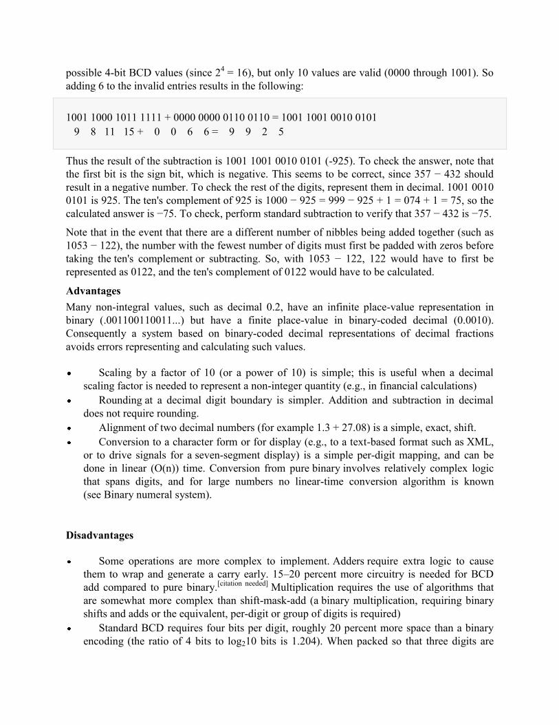
possible 4-bit BCD values (since 24 = 16), but only 10 values are valid (0000 through 1001). So adding 6 to the invalid entries results in the following:
1001 1000 1011 1111 + 0000 0000 0110 0110 = 1001 1001 0010 0101 9 8 11 15 + 0 0 6 6 = 9 9 2 5
Thus the result of the subtraction is 1001 1001 0010 0101 (-925). To check the answer, note that the first bit is the sign bit, which is negative. This seems to be correct, since 357 − 432 should
result in a negative number. To check the rest of the digits, represent them in decimal. 1001 0010 0101 is 925. The ten's complement of 925 is 1000 − 925 = 999 − 925 + 1 = 074 + 1 = 75, so the
calculated answer is −75. To check, perform standard subtraction to verify that 357 − 432 is −75.
Note that in the event that there are a different number of nibbles being added together (such as 1053 − 122), the number with the fewest number of digits must first be padded with zeros before
taking the ten's complement or subtracting. So, with 1053 − 122, 122 would have to first be
represented as 0122, and the ten's complement of 0122 would have to be calculated.
Advantages Many non-integral values, such as decimal 0.2, have an infinite place-value representation in binary (.001100110011...) but have a finite place-value in binary-coded decimal (0.0010). Consequently a system based on binary-coded decimal representations of decimal fractions avoids errors representing and calculating such values.
Scaling by a factor of 10 (or a power of 10) is simple; this is useful when a decimal scaling factor is needed to represent a non-integer quantity (e.g., in financial calculations)
Rounding at a decimal digit boundary is simpler. Addition and subtraction in decimal does not require rounding.
Alignment of two decimal numbers (for example 1.3 + 27.08) is a simple, exact, shift. Conversion to a character form or for display (e.g., to a text-based format such as XML,
or to drive signals for a seven-segment display) is a simple per-digit mapping, and can be done in linear (O(n)) time. Conversion from pure binary involves relatively complex logic that spans digits, and for large numbers no linear-time conversion algorithm is known (see Binary numeral system).
Disadvantages
Some operations are more complex to implement. Adders require extra logic to cause them to wrap and generate a carry early. 15–20 percent more circuitry is needed for BCD add compared to pure binary.[citation needed] Multiplication requires the use of algorithms that are somewhat more complex than shift-mask-add (a binary multiplication, requiring binary shifts and adds or the equivalent, per-digit or group of digits is required)
Standard BCD requires four bits per digit, roughly 20 percent more space than a binary encoding (the ratio of 4 bits to log210 bits is 1.204). When packed so that three digits are
encoded in ten bits, the storage overhead is greatly reduced, at the expense of an encoding that is unaligned with the 8-bit byte boundaries common on existing hardware, resulting in slower implementations on these systems.
Practical existing implementations of BCD are typically slower than operations on binary representations, especially on embedded systems,[citation needed] due to limited processor support for native BCD operations.
1.8.3. Application
The BIOS in many personal computers stores the date and time in BCD because the MC6818 real-time clock chip used in the original IBM PC AT motherboard provided the time encoded in BCD. This form is easily converted into ASCII for display.[8]
The Atari 8-bit family of computers used BCD to implement floating-point algorithms. The MOS 6502 processor used has a BCD mode that affects the addition and subtraction instructions.
Early models of the PlayStation 3 store the date and time in BCD. This led to a worldwide outage of the console on 1 March 2010. The last two digits of the year stored as BCD were misinterpreted as 16 causing an error in the unit's date, rendering most functions inoperable. This has been referred to as the Year 2010 Problem
1.9.Error Detection Code
In information theory and coding theory with applications in computer science and telecommunication, error detection and correction or error control are techniques that enable reliable delivery of digital data over unreliable communication channels. Many communication channels are subject to channel noise, and thus errors may be introduced during transmission from the source to a receiver. Error detection techniques allow detecting such errors, while error correction enables reconstruction of the original data.
1.9.1.Error detection schemes
Error detection is most commonly realized using a suitable hash function (or checksum algorithm). A hash function adds a fixed-length tag to a message, which enables receivers to verify the delivered message by recomputing the tag and comparing it with the one provided.
There exists a vast variety of different hash function designs. However, some are of particularly widespread use because of either their simplicity or their suitability for detecting certain kinds of errors (e.g., the cyclic redundancy check's performance in detecting burst errors).
Random-error-correcting codes based on minimum distance coding can provide a suitable alternative to hash functions when a strict guarantee on the minimum number of errors to be detected is desired. Repetition codes, described below, are special cases of error-correcting
codes: although rather inefficient, they find applications for both error correction and detection due to their simplicity.
1.9.2.Repetition codes A repetition code is a coding scheme that repeats the bits across a channel to achieve error-free communication. Given a stream of data to be transmitted, the data is divided into blocks of bits. Each block is transmitted some predetermined number of times. For example, to send the bit pattern "1011", the four-bit block can be repeated three times, thus producing "1011 1011 1011". However, if this twelve-bit pattern was received as "1010 1011 1011" – where the first block is unlike the other two – it can be determined that an error has occurred.
Repetition codes are very inefficient, and can be susceptible to problems if the error occurs in exactly the same place for each group (e.g., "1010 1010 1010" in the previous example would be detected as correct). The advantage of repetition codes is that they are extremely simple, and are in fact used in some transmissions of numbers stations.
1.9.3.Parity bits A parity bit is a bit that is added to a group of source bits to ensure that the number of set bits (i.e., bits with value 1) in the outcome is even or odd. It is a very simple scheme that can be used to detect single or any other odd number (i.e., three, five, etc.) of errors in the output. An even number of flipped bits will make the parity bit appear correct even though the data is erroneous. Extensions and variations on the parity bit mechanism are horizontal redundancy checks, vertical redundancy checks, and "double," "dual," or "diagonal" parity (used in RAID-DP).
1.9.4.Checksums A checksum of a message is a modular arithmetic sum of message code words of a fixed word length (e.g., byte values). The sum may be negated by means of a ones'-complement operation prior to transmission to detect errors resulting in all-zero messages.
Checksum schemes include parity bits, check digits, and longitudinal redundancy checks. Some checksum schemes, such as the Damm algorithm, the Luhn algorithm, and the Verhoeff algorithm, are specifically designed to detect errors commonly introduced by humans in writing down or remembering identification numbers.
1.9.5.Cyclic redundancy checks (CRCs) A cyclic redundancy check (CRC) is a single-burst-error-detecting cyclic code and non-secure hash function designed to detect accidental changes to digital data in computer networks. It is not suitable for detecting maliciously introduced errors. It is characterized by specification of a so-called generator polynomial, which is used as the divisor in a polynomial long division over a finite field, taking the input data as the dividend, and where the remainder becomes the result.
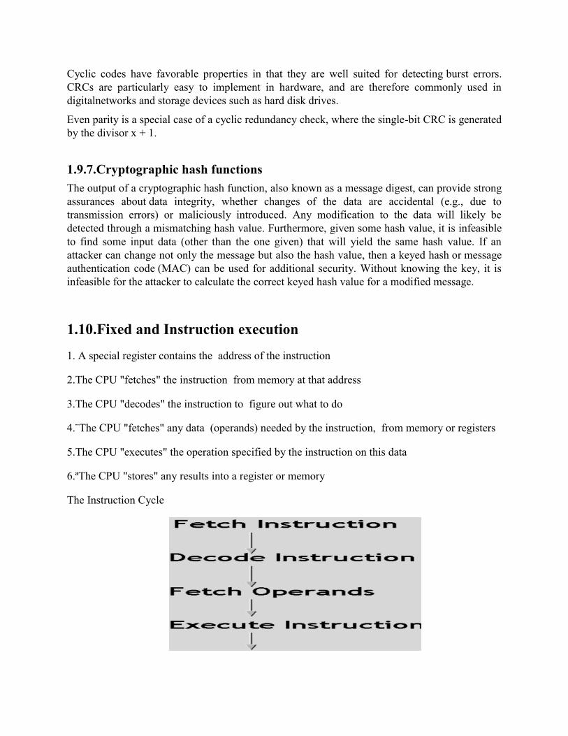
Cyclic codes have favorable properties in that they are well suited for detecting burst errors. CRCs are particularly easy to implement in hardware, and are therefore commonly used in digitalnetworks and storage devices such as hard disk drives.
Even parity is a special case of a cyclic redundancy check, where the single-bit CRC is generated by the divisor x + 1.
1.9.7.Cryptographic hash functions The output of a cryptographic hash function, also known as a message digest, can provide strong assurances about data integrity, whether changes of the data are accidental (e.g., due to transmission errors) or maliciously introduced. Any modification to the data will likely be detected through a mismatching hash value. Furthermore, given some hash value, it is infeasible to find some input data (other than the one given) that will yield the same hash value. If an attacker can change not only the message but also the hash value, then a keyed hash or message authentication code (MAC) can be used for additional security. Without knowing the key, it is infeasible for the attacker to calculate the correct keyed hash value for a modified message.
1.10.Fixed and Instruction execution
1. A special register contains the address of the instruction
2.The CPU "fetches" the instruction from memory at that address
3.The CPU "decodes" the instruction to figure out what to do
4.¨The CPU "fetches" any data (operands) needed by the instruction, from memory or registers
5.The CPU "executes" the operation specified by the instruction on this data
6.ªThe CPU "stores" any results into a register or memory
The Instruction Cycle
How Does a Complete Program Get Executed?
The "special register" is initialized to point to the first instruction of the program
• As part of the instruction fetch cycle, the "special register" is updated to point to the next instruction
• When one instruction is finished, the cycle is begun all over again
– the CPU never quits; it is always executing something
1.11.Interrupts
An interrupt is a signal from a device attached to a computer or from a program within the computer that causes the main program that operates the computer (the operating system ) to stop and figure out what to do next. Almost all personal (or larger) computers today areinterrupt-driven - that is, they start down the list of computer instruction s in one program (perhaps an application such as a word processor) and keep running the instructions until either (A) they can't go any further or (B) an interrupt signal is sensed. After the interrupt signal is sensed, the computer either resumes running the program it was running or begins running another program.
Basically, a single computer can perform only one computer instruction at a time. But, because it can be interrupted, it can take turns in which programs or sets of instructions that it performs. This is known as multitasking . It allows the user to do a number of different things at the same time. The computer simply takes turns managing the programs that the user effectively starts. Of course, the computer operates at speeds that make it seem as though all of the user's tasks are being performed at the same time. (The computer's operating system is good at using little pauses in operations and user think time to work on other programs.)
An operating system usually has some code that is called an interrupt handler . The interrupt handler prioritizes the interrupts and saves them in a queue if more than one is waiting to be handled. The operating system has another little program, sometimes called ascheduler , that figures out which program to give control to next.
In general, there are hardware interrupts and software interrupts. A hardware interrupt occurs, for example, when an I/O operation is completed such as reading some data into the computer from a tape drive. A software interrupt occurs when an application program terminates or requests certain services from the operating system. In a personal computer, a hardware interrupt request ( IRQ ) has a value associated with it that associates it with a particular device.
Types of interrupts
∗ Software interrupts
∗ Hardware interrupts
∗ Exceptions
1.Software interrupts
∗ Keyboard services
» int 21H DOS services
» int 16H BIOS services
2. Exceptions
∗ Single-step example
3. Hardware interrupts
∗ Accessing I/O
∗ Peripheral support chips
1.12.Buses
The CPU of personal computer has to send and receive various types of information and data to and from all other devices and components inside a computer and to devices connected to outer word of computer. If we remove the case of CPU then we will see that there is a mesh of wires or electronics pathways connected between motherboard and other components. These are the wires or electronics pathways that joins various components together to communicate with each other. This network of wires or electronics pathways is known as 'BUS'. Thus BUS is simply a set of wires of lines that connects various components inside a computer. Types of Buses:
Mainly, Computer's BUS can be divided into two types :
Internal Bus External Bus
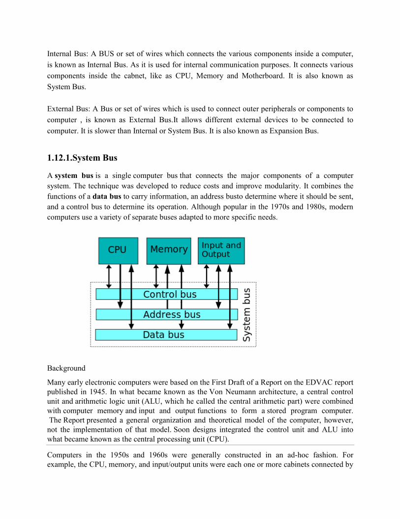
Internal Bus: A BUS or set of wires which connects the various components inside a computer, is known as Internal Bus. As it is used for internal communication purposes. It connects various components inside the cabnet, like as CPU, Memory and Motherboard. It is also known as System Bus. External Bus: A Bus or set of wires which is used to connect outer peripherals or components to computer , is known as External Bus.It allows different external devices to be connected to computer. It is slower than Internal or System Bus. It is also known as Expansion Bus.
1.12.1.System Bus
A system bus is a single computer bus that connects the major components of a computer system. The technique was developed to reduce costs and improve modularity. It combines the functions of a data bus to carry information, an address busto determine where it should be sent, and a control bus to determine its operation. Although popular in the 1970s and 1980s, modern computers use a variety of separate buses adapted to more specific needs.
Background
Many early electronic computers were based on the First Draft of a Report on the EDVAC report published in 1945. In what became known as the Von Neumann architecture, a central control unit and arithmetic logic unit (ALU, which he called the central arithmetic part) were combined with computer memory and input and output functions to form a stored program computer.
The Report presented a general organization and theoretical model of the computer, however, not the implementation of that model. Soon designs integrated the control unit and ALU into what became known as the central processing unit (CPU).
Computers in the 1950s and 1960s were generally constructed in an ad-hoc fashion. For example, the CPU, memory, and input/output units were each one or more cabinets connected by
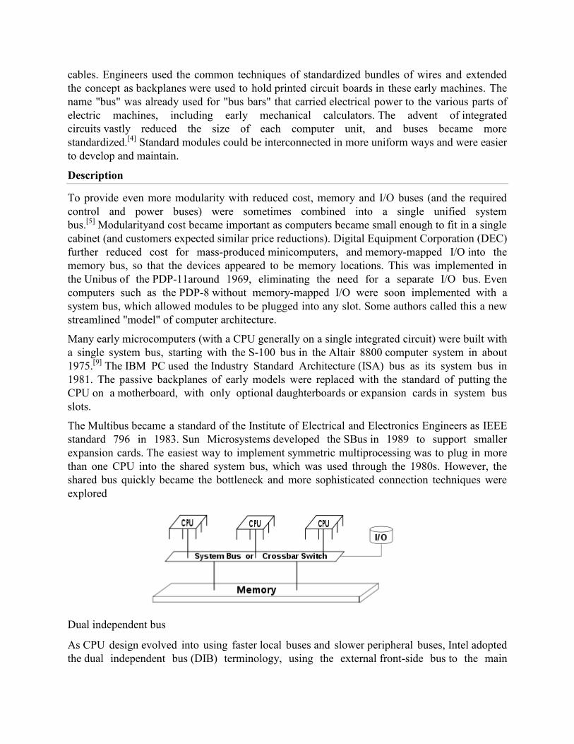
cables. Engineers used the common techniques of standardized bundles of wires and extended the concept as backplanes were used to hold printed circuit boards in these early machines. The name "bus" was already used for "bus bars" that carried electrical power to the various parts of electric machines, including early mechanical calculators. The advent of integrated circuits vastly reduced the size of each computer unit, and buses became more standardized.[4] Standard modules could be interconnected in more uniform ways and were easier to develop and maintain.
Description
To provide even more modularity with reduced cost, memory and I/O buses (and the required control and power buses) were sometimes combined into a single unified system bus.[5] Modularityand cost became important as computers became small enough to fit in a single cabinet (and customers expected similar price reductions). Digital Equipment Corporation (DEC) further reduced cost for mass-produced minicomputers, and memory-mapped I/O into the memory bus, so that the devices appeared to be memory locations. This was implemented in the Unibus of the PDP-11around 1969, eliminating the need for a separate I/O bus. Even computers such as the PDP-8 without memory-mapped I/O were soon implemented with a system bus, which allowed modules to be plugged into any slot. Some authors called this a new streamlined "model" of computer architecture.
Many early microcomputers (with a CPU generally on a single integrated circuit) were built with a single system bus, starting with the S-100 bus in the Altair 8800 computer system in about 1975.[9] The IBM PC used the Industry Standard Architecture (ISA) bus as its system bus in 1981. The passive backplanes of early models were replaced with the standard of putting the CPU on a motherboard, with only optional daughterboards or expansion cards in system bus slots.
The Multibus became a standard of the Institute of Electrical and Electronics Engineers as IEEE standard 796 in 1983. Sun Microsystems developed the SBus in 1989 to support smaller expansion cards. The easiest way to implement symmetric multiprocessing was to plug in more than one CPU into the shared system bus, which was used through the 1980s. However, the shared bus quickly became the bottleneck and more sophisticated connection techniques were explored
Dual independent bus
As CPU design evolved into using faster local buses and slower peripheral buses, Intel adopted the dual independent bus (DIB) terminology, using the external front-side bus to the main
system memory, and the internal back-side bus between one or more CPUs and the CPU caches. This was introduced in the Pentium Pro and Pentium II products in the mid to late 1990s.
The primary bus for communicating data between the CPU and main memory and input and output devices is called the front-side bus, and the back-side bus accesses the level 2 cache. Modern personal and server computers use higher-performance interconnection technologies such as HyperTransport and Intel QuickPath Interconnect, while the system bus architecture continued to be used on simpler embedded microprocessors. The systems bus can even be internal to a single integrated circuit, producing asystem-on-a-chip. Examples include AMBA, CoreConnect, and Wishbone.
1.13.Boolean Algebra
In 1854 George Boole introduced a systematic approach of logic and developed an algebraic system to treat the logic functions, which is now called Boolean algebra. In 1938 C.E. Shannon developed a two-valued Boolean algebra called Switching algebra, and demonstrated that the properties of two-valued or bistable electrical switching circuits can be represented by this algebra. The postulates formulated by E.V. Huntington in 1904 are employed for the formal definition of Boolean algebra. However, Huntington postulates are not unique for defining Boolean algebra and other postulates are also used. The following Huntington postulates are satisfied for the definition of Boolean algebra on a set of elements S together with two binary operators (+) and (.).
1. (a) Closer with respect to the operator (+). (b) Closer with respect to the operator (.).
2. (a) An identity element with respect to + is designated by 0 i.e., A + 0 = 0 + A = A. (b) An identity element with respect to . is designated by 1 i.e., A.1 = 1. A = A.
3. (a) Commutative with respect to (+), i.e., A + B = B + A. (b) Commutative with respect to (.), i.e., A.B = B.A.
4. (a) (.) is distributive over (+), i.e., A . (B+C) = (A . B) + (A . C). (b) (+) is distributive over (.), i.e., A + (B .C) = (A + B) . (A + C).
5. For every element A ∈ S, there exists an element A' ∈ S (called the complement of A) such that A + A′ = 1 and A . A′ = 0. 6. There exists at least two elements A,B ∈ S, such that A is not equal to B.
Comparing Boolean algebra with arithmetic and ordinary algebra (the field of real numbers), the following differences are observed:
1. Huntington postulates do not include the associate law. However, Boolean algebra follows the law and can be derived from the other postulates for both operations.
2. The distributive law of (+) over ( . ) i.e., A+ (B.C) = (A+B) . (A+C) is valid for Boolean algebra, but not for ordinary algebra. 3. Boolean algebra does not have additive or multiplicative inverses, so there are no subtraction or division operations. 4. Postulate 5 defines an operator called Complement, which is not available in ordinary algebra. 5. Ordinary algebra deals with real numbers, which consist of an infinite set of elements. Boolean algebra deals with the as yet undefined set of elements S, but in the two valued Boolean algebra, the set S consists of only two elements—0 and 1.
Boolean algebra is very much similar to ordinary algebra in some respects. The symbols (+) and (.) are chosen intentionally to facilitate Boolean algebraic manipulations by persons already familiar to ordinary algebra. Although one can use some knowledge from ordinary algebra to deal with Boolean algebra, beginners must be careful not to substitute the rules of ordinary algebra where they are not applicable.
It is important to distinguish between the elements of the set of an algebraic structure and the variables of an algebraic system. For example, the elements of the field of real numbers are numbers, the variables such as X, Y, Z, etc., are the symbols that stand for real numbers, which are used in ordinary algebra. On the other hand, in the case of Boolean algebra, the elements of a set S are defined, and the variables A, B, C, etc., are merely symbols that represent the elements. At this point, it is important to realize that in order to have Boolean algebra, the following must be shown. 1. The elements of the set S. 2. The rules of operation for the two binary operators. 3. The set of elements S, together with the two operators satisfies six Huntington postulates.
One may formulate much Boolean algebra, depending on the choice of elements of set S and the rules of operation. In the subsequent chapters, we will only deal with a two-valued Boolean algebra i.e., one with two elements. Two-valued Boolean algebra has the applications in set theory and propositional logic. But here, our interest is with the application of Boolean algebra to gate-type logic circuits. 1.13.1 Basic Properties And Theorems Of Boolean Algebra 1.13.1.1 Principle of Duality From Huntington postulates, it is evident that they are grouped in pairs as (a) and (b) and every algebraic expression deductible from the postulates of Boolean algebra remains valid if the operators and identity elements are interchanged. This means one expression can be obtained from the other in each pair by interchanging every element i.e., every 0 with 1, every 1 with 0, as
well as interchanging the operators i.e., every (+) with (.) and every (.) with (+). This important property of Boolean algebra is called principle of duality. 1.13.1.2 DeMorgan's Theorem Two theorems that were proposed by DeMorgan play important parts in Boolean algebra. The first theorem states that the complement of a product is equal to the sum of the complements. That is, if the variables are A and B, then
(A.B)′ = A′ + B′ The second theorem states that the complement of a sum is equal to the product of the complements. In equation form, this can be expressed as
(A + B)′ = A′ . B′ The complements of Boolean logic function or a logic expression may be simplified or expanded by the following steps of DeMorgan‘s theorem.
(a) Replace the operator (+) with (.) and (.) with (+) given in the expression. (b) Complement each of the terms or variables in the expression.
DeMorgan‘s theorems are applicable to any number of variables. For three variables A, B, and C, the equations are
(A.B.C)′ = A′ + B′ + C′ and (A + B + C)′ = A′.B′.C′
1.13.1.3 Other Important Theorems Theorem 1(a): A + A = A
A + A = (A + A).1 by postulate 2(b) = (A + A) . ( A + A′) by postulate 5 = A + A.A′ = A + 0 by postulate 4 = A by postulate 2(a)
Theorem 1(b): A . A = A
A . A = (A . A) + 0 by postulate 2(a) = (A . A) + ( A . A′) by postulate 5 = A (A + A′) = A . 1 by postulate 4
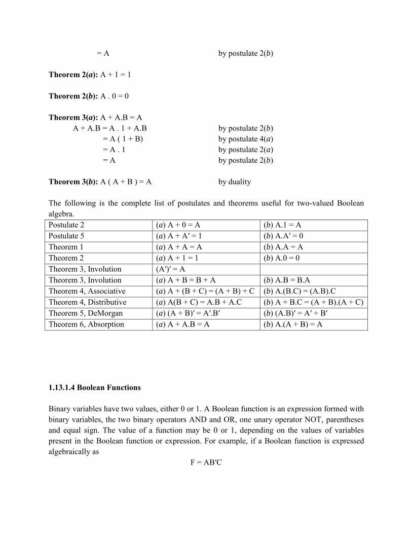
= A by postulate 2(b) Theorem 2(a): A + 1 = 1 Theorem 2(b): A . 0 = 0 Theorem 3(a): A + A.B = A
A + A.B = A . 1 + A.B by postulate 2(b) = A ( 1 + B) by postulate 4(a) = A . 1 by postulate 2(a) = A by postulate 2(b)
Theorem 3(b): A ( A + B ) = A by duality The following is the complete list of postulates and theorems useful for two-valued Boolean algebra. Postulate 2 (a) A + 0 = A (b) A.1 = A Postulate 5 (a) A + A′ = 1 (b) A.A′ = 0 Theorem 1 (a) A + A = A (b) A.A = A Theorem 2 (a) A + 1 = 1 (b) A.0 = 0 Theorem 3, Involution (A′)′ = A Theorem 3, Involution (a) A + B = B + A (b) A.B = B.A Theorem 4, Associative (a) A + (B + C) = (A + B) + C (b) A.(B.C) = (A.B).C Theorem 4, Distributive (a) A(B + C) = A.B + A.C (b) A + B.C = (A + B).(A + C) Theorem 5, DeMorgan (a) (A + B)′ = A′.B′ (b) (A.B)′ = A′ + B′ Theorem 6, Absorption (a) A + A.B = A (b) A.(A + B) = A 1.13.1.4 Boolean Functions Binary variables have two values, either 0 or 1. A Boolean function is an expression formed with binary variables, the two binary operators AND and OR, one unary operator NOT, parentheses and equal sign. The value of a function may be 0 or 1, depending on the values of variables present in the Boolean function or expression. For example, if a Boolean function is expressed algebraically as
F = AB′C
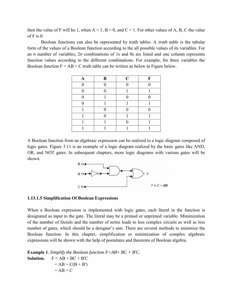
then the value of F will be 1, when A = 1, B = 0, and C = 1. For other values of A, B, C the value of F is 0.
Boolean functions can also be represented by truth tables. A truth table is the tabular form of the values of a Boolean function according to the all possible values of its variables. For an n number of variables, 2n combinations of 1s and 0s are listed and one column represents function values according to the different combinations. For example, for three variables the Boolean function F = AB + C truth table can be written as below in Figure below.
A B C F 0 0 0 0 0 0 1 1 0 1 0 0 0 1 1 1 1 0 0 0 1 0 1 1 1 1 0 1 1 1 1 1
A Boolean function from an algebraic expression can be realized to a logic diagram composed of logic gates. Figure 3.11 is an example of a logic diagram realized by the basic gates like AND, OR, and NOT gates. In subsequent chapters, more logic diagrams with various gates will be shown.
1.13.1.5 Simplification Of Boolean Expressions When a Boolean expression is implemented with logic gates, each literal in the function is designated as input to the gate. The literal may be a primed or unprimed variable. Minimization of the number of literals and the number of terms leads to less complex circuits as well as less number of gates, which should be a designer‘s aim. There are several methods to minimize the Boolean function. In this chapter, simplification or minimization of complex algebraic expressions will be shown with the help of postulates and theorems of Boolean algebra. Example 1. Simplify the Boolean function F=AB+ BC + B′C.
Solution. F = AB + BC + B′C = AB + C(B + B′) = AB + C
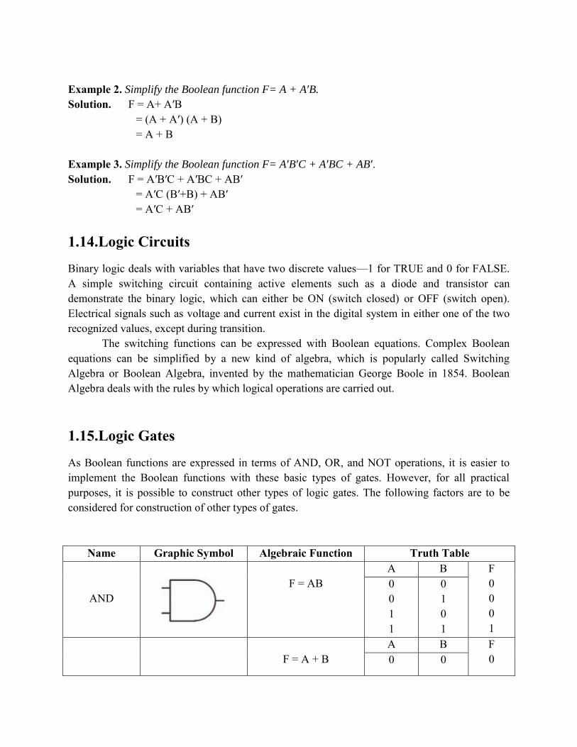
Example 2. Simplify the Boolean function F= A + A′B.
Solution. F = A+ A′B = (A + A′) (A + B) = A + B
Example 3. Simplify the Boolean function F= A′B′C + A′BC + AB′. Solution. F = A′B′C + A′BC + AB′
= A′C (B′+B) + AB′ = A′C + AB′
1.14.Logic Circuits
Binary logic deals with variables that have two discrete values—1 for TRUE and 0 for FALSE. A simple switching circuit containing active elements such as a diode and transistor can demonstrate the binary logic, which can either be ON (switch closed) or OFF (switch open). Electrical signals such as voltage and current exist in the digital system in either one of the two recognized values, except during transition.
The switching functions can be expressed with Boolean equations. Complex Boolean equations can be simplified by a new kind of algebra, which is popularly called Switching Algebra or Boolean Algebra, invented by the mathematician George Boole in 1854. Boolean Algebra deals with the rules by which logical operations are carried out.
1.15.Logic Gates
As Boolean functions are expressed in terms of AND, OR, and NOT operations, it is easier to implement the Boolean functions with these basic types of gates. However, for all practical purposes, it is possible to construct other types of logic gates. The following factors are to be considered for construction of other types of gates.
Name Graphic Symbol Algebraic Function Truth Table
AND
F = AB
A B F 0 0 0 1
0 0 1 1
0 1 0 1
F = A + B
A B F 0 0 0
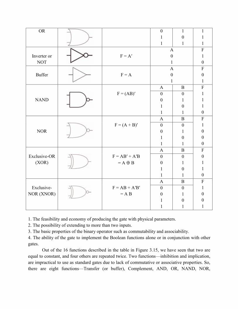
OR
0 1 1
1 0 1
1 1 1
Inverter or
NOT
F = A′
A 0 1
F 1 0
Buffer
F = A
A 0 1
F 0 1
NAND
F = (AB)′
A B F 1 1 1 0
0 0 1 1
0 1 0 1
NOR
F = (A + B)′
A B F 1 0 0 0
0 0 1 1
0 1 0 1
Exclusive-OR
(XOR)
F = AB′ + A′B
= A B
A B F 0 1 1 0
0 0 1 1
0 1 0 1
Exclusive-
NOR (XNOR)
F = AB + A′B′
= A B
A B F 1 0 0 1
0 0 1 1
0 1 0 1
1. The feasibility and economy of producing the gate with physical parameters. 2. The possibility of extending to more than two inputs. 3. The basic properties of the binary operator such as commutability and associability. 4. The ability of the gate to implement the Boolean functions alone or in conjunction with other gates.
Out of the 16 functions described in the table in Figure 3.15, we have seen that two are equal to constant, and four others are repeated twice. Two functions—inhibition and implication, are impractical to use as standard gates due to lack of commutative or associative properties. So, there are eight functions—Transfer (or buffer), Complement, AND, OR, NAND, NOR,
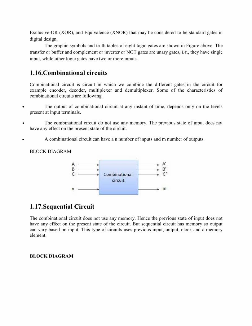
Exclusive-OR (XOR), and Equivalence (XNOR) that may be considered to be standard gates in digital design.
The graphic symbols and truth tables of eight logic gates are shown in Figure above. The transfer or buffer and complement or inverter or NOT gates are unary gates, i.e., they have single input, while other logic gates have two or more inputs.
1.16.Combinational circuits
Combinational circuit is circuit in which we combine the different gates in the circuit for example encoder, decoder, multiplexer and demultiplexer. Some of the characteristics of combinational circuits are following.
The output of combinational circuit at any instant of time, depends only on the levels present at input terminals.
The combinational circuit do not use any memory. The previous state of input does not have any effect on the present state of the circuit.
A combinational circuit can have a n number of inputs and m number of outputs.
BLOCK DIAGRAM
1.17.Sequential Circuit
The combinational circuit does not use any memory. Hence the previous state of input does not have any effect on the present state of the circuit. But sequential circuit has memory so output can vary based on input. This type of circuits uses previous input, output, clock and a memory element.
BLOCK DIAGRAM
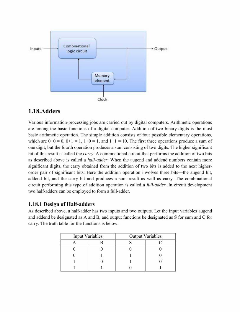
1.18.Adders
Various information-processing jobs are carried out by digital computers. Arithmetic operations are among the basic functions of a digital computer. Addition of two binary digits is the most basic arithmetic operation. The simple addition consists of four possible elementary operations, which are 0+0 = 0, 0+1 = 1, 1+0 = 1, and 1+1 = 10. The first three operations produce a sum of one digit, but the fourth operation produces a sum consisting of two digits. The higher significant bit of this result is called the carry. A combinational circuit that performs the addition of two bits as described above is called a half-adder. When the augend and addend numbers contain more significant digits, the carry obtained from the addition of two bits is added to the next higher-order pair of significant bits. Here the addition operation involves three bits—the augend bit, addend bit, and the carry bit and produces a sum result as well as carry. The combinational circuit performing this type of addition operation is called a full-adder. In circuit development two half-adders can be employed to form a full-adder. 1.18.1 Design of Half-adders As described above, a half-adder has two inputs and two outputs. Let the input variables augend and addend be designated as A and B, and output functions be designated as S for sum and C for carry. The truth table for the functions is below.
Input Variables Output Variables A B S C 0 0 1 1
0 1 0 1
0 1 1 0
0 0 0 1
From the truth table in Figure 5.2, it can be seen that the outputs S and C functions are similar to Exclusive-OR and AND functions respectively, as shown in Figure below. The Boolean expressions are
S = A′B+AB′ and C = AB.
Figure below shows the logic diagram to implement the half-adder circuit.
1.18.2 Design of Full-adders A combinational circuit of full-adder performs the operation of addition of three bits—the augend, addend, and previous carry, and produces the outputs sum and carry. Let us designate the input variables augend as A, addend as B, and previous carry as X, and outputs sum as S and carry as C. As there are three input variables, eight different input combinations are possible. The truth table is shown below according to its functions.
Input Variables Output Variables X A B S C 0 0 0 0 1 1 1 1
0 0 1 1 0 0 1 1
0 1 0 1 0 1 0 1
0 1 1 0 1 0 0 1
0 0 0 1 0 1 1 1
To derive the simplified Boolean expression from the truth table, the Karnaugh map method is adopted as in shown below. A′ B′ A′B AB AB′
X′ X Map for function S A′ B′ A′B AB AB′ X′ X Map for function C The simplified Boolean expressions of the outputs are
S = X′A′B + X′AB′ + XA′B′ + XAB and C = AB + BX + AX.
The logic diagram for the above functions is shown below. It is assumed complements of X, A, and B are available at the input source.
Note that one type of configuration of the combinational circuit diagram for full-adder is
realized in below, with two-input and three-input AND gates, and three input and four-input OR gates. Other configurations can also be developed where number and type of gates are reduced. For this, the Boolean expressions of S and C are modified as follows.
S = X′A′B + X′AB′ + XA′B′ + XAB = X′ (A′B + AB′) + X (A′B′ + AB) = X′ (A B) + X (A B)′ = X A B
C = AB + BX + AX = AB + X (A + B) = AB + X (AB + AB′ + AB + A′B) = AB + X (AB + AB′ + A‘B) = AB + XAB + X (AB′ + A‘B) = AB + X (A B)
1 1 1 1
1 1 1 1
Logic diagram according to the modified expression is
You may notice that the full-adder developed in above Figure consists of two 2-input AND gates, two 2-input XOR (Exclusive-OR) gates and one 2-input OR gate. This contains a reduced number of gates as well as type of gates as compared to actual Figure. Also, if compared with a half-adder circuit, the full-adder circuit can be formed with two half-adders and one OR gate.
1.19.Decoders
A Decoder is the exact opposite to that of an "Encoder" we looked at in the last tutorial. It is basically, a combinational type logic circuit that converts the binary code data at its input into one of a number of different output lines, one at a time producing an equivalent decimal code at its output. Binary Decodershave inputs of 2-bit, 3-bit or 4-bit codes depending upon the number of data input lines, and a n-bitdecoder has 2n output lines.
Therefore, if a binary decoder receives n inputs (usually grouped as a binary or Boolean number) it activates one and only one of its 2n outputs based on that input with all other outputs deactivated. A decoders output code normally has more bits than its input code and practical "binary decoder" circuits include, 2-to-4, 3-to-8 and 4-to-16 line configurations.
A Binary Decoder converts coded inputs into coded outputs, where the input and output codes are different and decoders are available to "decode" either a Binary or BCD (8421 code) input pattern to typically a Decimal output code. Commonly available BCD-to-Decimal decoders include the TTL 7442 or the CMOS 4028. An example of a 2-to-4 line decoder along with its truth table is given below. It consists of an array of four NAND gates, one of which is selected for each combination of the input signals A and B.
1.19.1.A 2-to-4 Binary Decoders.
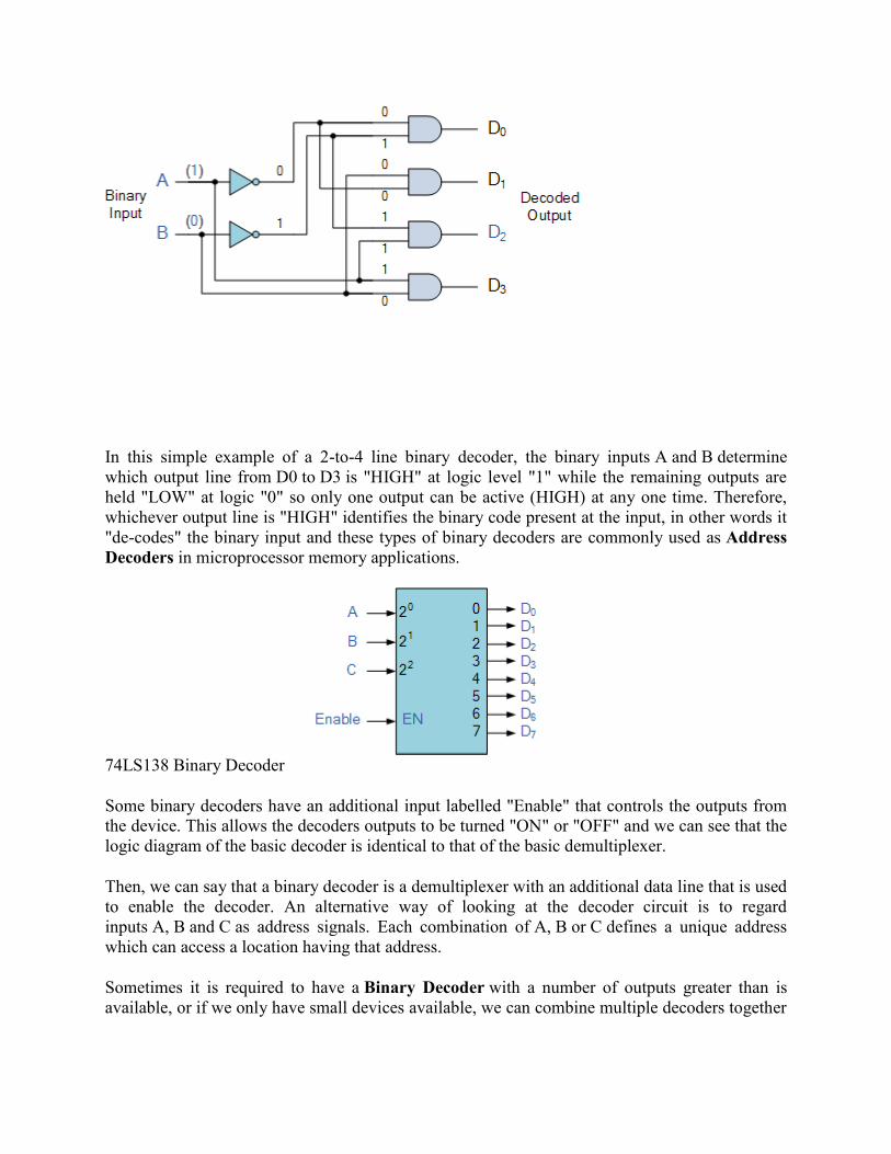
In this simple example of a 2-to-4 line binary decoder, the binary inputs A and B determine which output line from D0 to D3 is "HIGH" at logic level "1" while the remaining outputs are held "LOW" at logic "0" so only one output can be active (HIGH) at any one time. Therefore, whichever output line is "HIGH" identifies the binary code present at the input, in other words it "de-codes" the binary input and these types of binary decoders are commonly used as Address Decoders in microprocessor memory applications.
74LS138 Binary Decoder
Some binary decoders have an additional input labelled "Enable" that controls the outputs from the device. This allows the decoders outputs to be turned "ON" or "OFF" and we can see that the logic diagram of the basic decoder is identical to that of the basic demultiplexer.
Then, we can say that a binary decoder is a demultiplexer with an additional data line that is used to enable the decoder. An alternative way of looking at the decoder circuit is to regard inputs A, B and C as address signals. Each combination of A, B or C defines a unique address which can access a location having that address.
Sometimes it is required to have a Binary Decoder with a number of outputs greater than is available, or if we only have small devices available, we can combine multiple decoders together
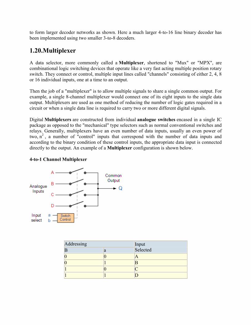
to form larger decoder networks as shown. Here a much larger 4-to-16 line binary decoder has been implemented using two smaller 3-to-8 decoders.
1.20.Multiplexer
A data selector, more commonly called a Multiplexer, shortened to "Mux" or "MPX", are combinational logic switching devices that operate like a very fast acting multiple position rotary switch. They connect or control, multiple input lines called "channels" consisting of either 2, 4, 8 or 16 individual inputs, one at a time to an output.
Then the job of a "multiplexer" is to allow multiple signals to share a single common output. For example, a single 8-channel multiplexer would connect one of its eight inputs to the single data output. Multiplexers are used as one method of reducing the number of logic gates required in a circuit or when a single data line is required to carry two or more different digital signals.
Digital Multiplexers are constructed from individual analogue switches encased in a single IC package as opposed to the "mechanical" type selectors such as normal conventional switches and relays. Generally, multiplexers have an even number of data inputs, usually an even power of two, n2 , a number of "control" inputs that correspond with the number of data inputs and according to the binary condition of these control inputs, the appropriate data input is connected directly to the output. An example of a Multiplexer configuration is shown below.
4-to-1 Channel Multiplexer
Addressing Input Selected B a
0 0 A 0 1 B 1 0 C 1 1 D
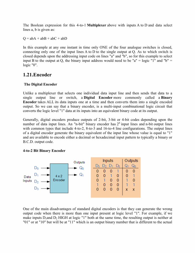
The Boolean expression for this 4-to-1 Multiplexer above with inputs A to D and data select lines a, b is given as:
Q = abA + abB + abC + abD
In this example at any one instant in time only ONE of the four analogue switches is closed, connecting only one of the input lines A to D to the single output at Q. As to which switch is closed depends upon the addressing input code on lines "a" and "b", so for this example to select input B to the output at Q, the binary input address would need to be "a" = logic "1" and "b" = logic "0".
1.21.Encoder
The Digital Encoder
Unlike a multiplexer that selects one individual data input line and then sends that data to a single output line or switch, a Digital Encoder more commonly called a Binary Encoder takes ALL its data inputs one at a time and then converts them into a single encoded output. So we can say that a binary encoder, is a multi-input combinational logic circuit that converts the logic level "1" data at its inputs into an equivalent binary code at its output.
Generally, digital encoders produce outputs of 2-bit, 3-bit or 4-bit codes depending upon the number of data input lines. An "n-bit" binary encoder has 2n input lines and n-bit output lines with common types that include 4-to-2, 8-to-3 and 16-to-4 line configurations. The output lines of a digital encoder generate the binary equivalent of the input line whose value is equal to "1" and are available to encode either a decimal or hexadecimal input pattern to typically a binary or B.C.D. output code.
4-to-2 Bit Binary Encoder
One of the main disadvantages of standard digital encoders is that they can generate the wrong output code when there is more than one input present at logic level "1". For example, if we make inputs D1and D2 HIGH at logic "1" both at the same time, the resulting output is neither at "01" or at "10" but will be at "11" which is an output binary number that is different to the actual
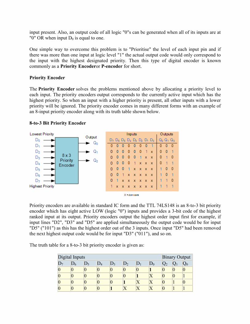
input present. Also, an output code of all logic "0"s can be generated when all of its inputs are at "0" OR when input D0 is equal to one.
One simple way to overcome this problem is to "Prioritise" the level of each input pin and if there was more than one input at logic level "1" the actual output code would only correspond to the input with the highest designated priority. Then this type of digital encoder is known commonly as a Priority Encoderor P-encoder for short.
Priority Encoder
The Priority Encoder solves the problems mentioned above by allocating a priority level to each input. The priority encoders output corresponds to the currently active input which has the highest priority. So when an input with a higher priority is present, all other inputs with a lower priority will be ignored. The priority encoder comes in many different forms with an example of an 8-input priority encoder along with its truth table shown below.
8-to-3 Bit Priority Encoder
Priority encoders are available in standard IC form and the TTL 74LS148 is an 8-to-3 bit priority encoder which has eight active LOW (logic "0") inputs and provides a 3-bit code of the highest ranked input at its output. Priority encoders output the highest order input first for example, if input lines "D2", "D3" and "D5" are applied simultaneously the output code would be for input "D5" ("101") as this has the highest order out of the 3 inputs. Once input "D5" had been removed the next highest output code would be for input "D3" ("011"), and so on.
The truth table for a 8-to-3 bit priority encoder is given as:
Digital Inputs Binary Output D7 D6 D5 D4 D3 D2 D1 D0 Q2 Q1 Q0 0 0 0 0 0 0 0 1 0 0 0 0 0 0 0 0 0 1 X 0 0 1 0 0 0 0 0 1 X X 0 1 0 0 0 0 0 1 X X X 0 1 1
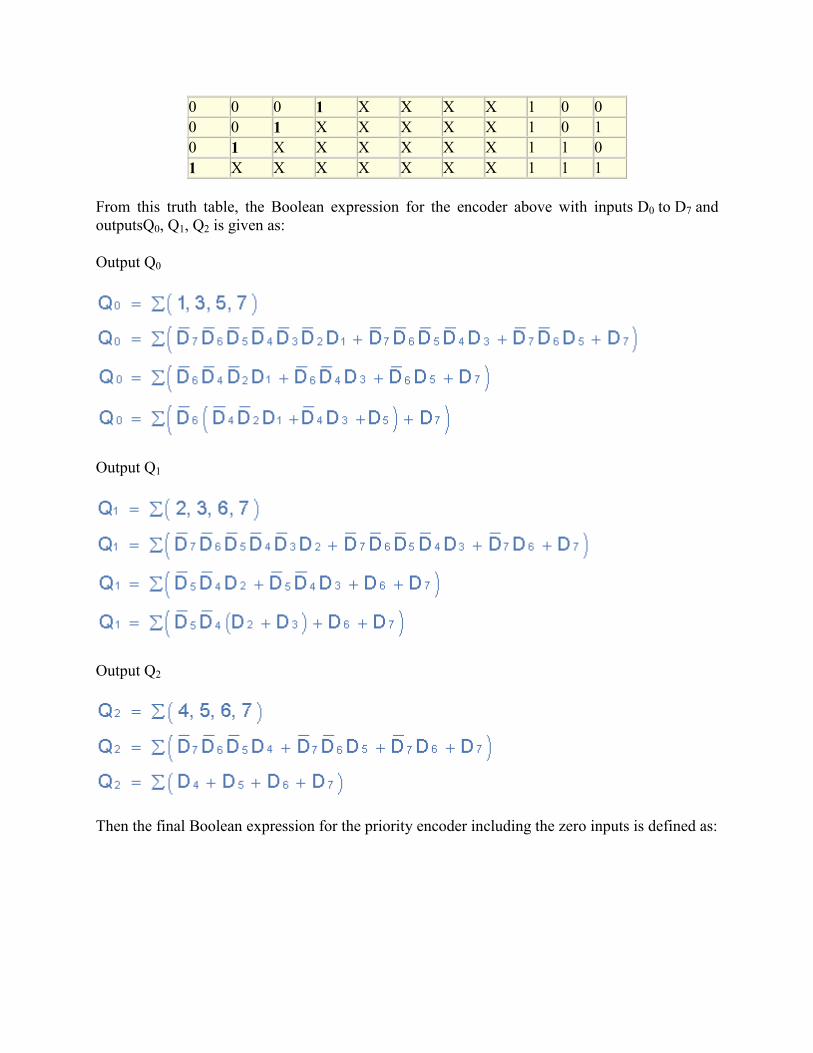
0 0 0 1 X X X X 1 0 0 0 0 1 X X X X X 1 0 1 0 1 X X X X X X 1 1 0 1 X X X X X X X 1 1 1
From this truth table, the Boolean expression for the encoder above with inputs D0 to D7 and outputsQ0, Q1, Q2 is given as:
Output Q0
Output Q1
Output Q2
Then the final Boolean expression for the priority encoder including the zero inputs is defined as:
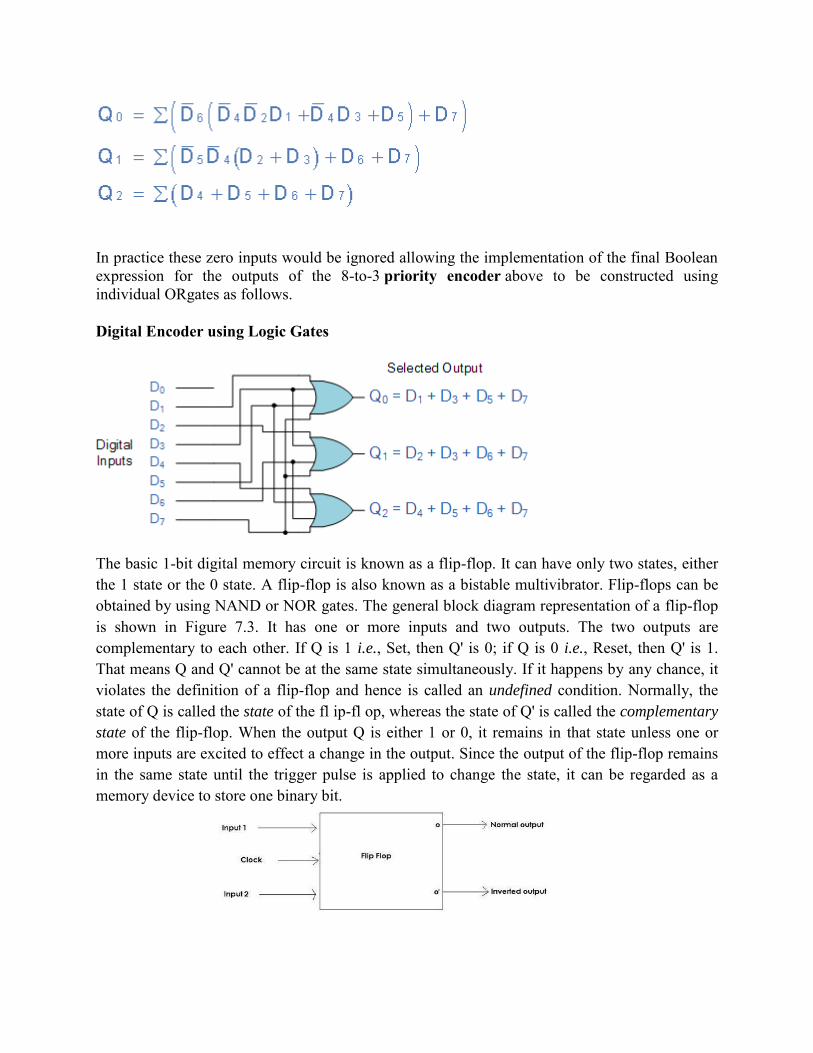
In practice these zero inputs would be ignored allowing the implementation of the final Boolean expression for the outputs of the 8-to-3 priority encoder above to be constructed using individual ORgates as follows.
Digital Encoder using Logic Gates
The basic 1-bit digital memory circuit is known as a flip-flop. It can have only two states, either the 1 state or the 0 state. A flip-flop is also known as a bistable multivibrator. Flip-flops can be obtained by using NAND or NOR gates. The general block diagram representation of a flip-flop is shown in Figure 7.3. It has one or more inputs and two outputs. The two outputs are complementary to each other. If Q is 1 i.e., Set, then Q' is 0; if Q is 0 i.e., Reset, then Q' is 1. That means Q and Q' cannot be at the same state simultaneously. If it happens by any chance, it violates the definition of a flip-flop and hence is called an undefined condition. Normally, the state of Q is called the state of the fl ip-fl op, whereas the state of Q' is called the complementary
state of the flip-flop. When the output Q is either 1 or 0, it remains in that state unless one or more inputs are excited to effect a change in the output. Since the output of the flip-flop remains in the same state until the trigger pulse is applied to change the state, it can be regarded as a memory device to store one binary bit.
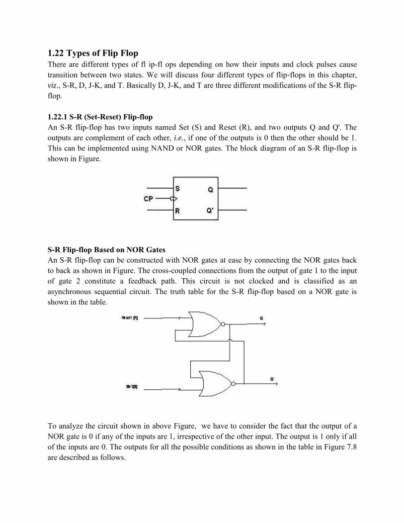
1.22 Types of Flip Flop There are different types of fl ip-fl ops depending on how their inputs and clock pulses cause transition between two states. We will discuss four different types of flip-flops in this chapter, viz., S-R, D, J-K, and T. Basically D, J-K, and T are three different modifications of the S-R flip-flop. 1.22.1 S-R (Set-Reset) Flip-flop An S-R flip-flop has two inputs named Set (S) and Reset (R), and two outputs Q and Q'. The outputs are complement of each other, i.e., if one of the outputs is 0 then the other should be 1. This can be implemented using NAND or NOR gates. The block diagram of an S-R flip-flop is shown in Figure.
S-R Flip-flop Based on NOR Gates An S-R flip-flop can be constructed with NOR gates at ease by connecting the NOR gates back to back as shown in Figure. The cross-coupled connections from the output of gate 1 to the input of gate 2 constitute a feedback path. This circuit is not clocked and is classified as an asynchronous sequential circuit. The truth table for the S-R flip-flop based on a NOR gate is shown in the table.
To analyze the circuit shown in above Figure, we have to consider the fact that the output of a NOR gate is 0 if any of the inputs are 1, irrespective of the other input. The output is 1 only if all of the inputs are 0. The outputs for all the possible conditions as shown in the table in Figure 7.8 are described as follows.
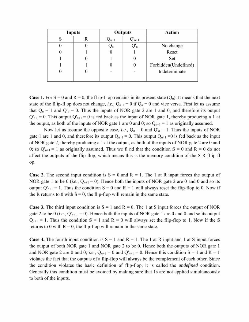
Inputs Outputs Action S R Qn+1 Q'n+1 0 0 1 1 0
0 1 0 1 0
Qn 0 1 0 -
Q'n 1 0 0 -
No change Reset Set
Forbidden(Undefined) Indeterminate
Case 1. For S = 0 and R = 0, the fl ip-fl op remains in its present state (Qn). It means that the next state of the fl ip-fl op does not change, i.e., Qn+1 = 0 if Qn = 0 and vice versa. First let us assume that Qn = 1 and Q'n = 0. Thus the inputs of NOR gate 2 are 1 and 0, and therefore its output Q'n+1= 0. This output Q'n+1 = 0 is fed back as the input of NOR gate 1, thereby producing a 1 at the output, as both of the inputs of NOR gate 1 are 0 and 0; so Qn+1 = 1 as originally assumed.
Now let us assume the opposite case, i.e., Qn = 0 and Q'n = 1. Thus the inputs of NOR gate 1 are 1 and 0, and therefore its output Qn+1 = 0. This output Qn+1 =0 is fed back as the input of NOR gate 2, thereby producing a 1 at the output, as both of the inputs of NOR gate 2 are 0 and 0; so Q'n+1 = 1 as originally assumed. Thus we fi nd that the condition S = 0 and R = 0 do not affect the outputs of the flip-flop, which means this is the memory condition of the S-R fl ip-fl op. Case 2. The second input condition is S = 0 and R = 1. The 1 at R input forces the output of NOR gate 1 to be 0 (i.e., Qn+1 = 0). Hence both the inputs of NOR gate 2 are 0 and 0 and so its output Q'n+1 = 1. Thus the condition S = 0 and R = 1 will always reset the flip-flop to 0. Now if the R returns to 0 with S = 0, the flip-flop will remain in the same state. Case 3. The third input condition is S = 1 and R = 0. The 1 at S input forces the output of NOR gate 2 to be 0 (i.e., Q'n+1 = 0). Hence both the inputs of NOR gate 1 are 0 and 0 and so its output Qn+1 = 1. Thus the condition S = 1 and R = 0 will always set the flip-flop to 1. Now if the S returns to 0 with R = 0, the flip-flop will remain in the same state. Case 4. The fourth input condition is S = 1 and R = 1. The 1 at R input and 1 at S input forces the output of both NOR gate 1 and NOR gate 2 to be 0. Hence both the outputs of NOR gate 1 and NOR gate 2 are 0 and 0; i.e., Qn+1 = 0 and Q'n+1 = 0. Hence this condition S = 1 and R = 1 violates the fact that the outputs of a flip-flop will always be the complement of each other. Since the condition violates the basic definition of flip-flop, it is called the undefined condition. Generally this condition must be avoided by making sure that 1s are not applied simultaneously to both of the inputs.
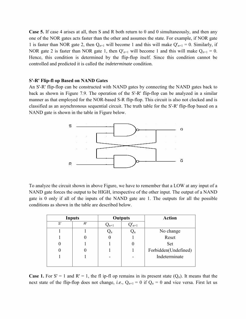
Case 5. If case 4 arises at all, then S and R both return to 0 and 0 simultaneously, and then any one of the NOR gates acts faster than the other and assumes the state. For example, if NOR gate 1 is faster than NOR gate 2, then Qn+1 will become 1 and this will make Q'n+1 = 0. Similarly, if NOR gate 2 is faster than NOR gate 1, then Q'n+1 will become 1 and this will make Qn+1 = 0. Hence, this condition is determined by the flip-flop itself. Since this condition cannot be controlled and predicted it is called the indeterminate condition.
S'-R' Flip-fl op Based on NAND Gates An S'-R' flip-flop can be constructed with NAND gates by connecting the NAND gates back to back as shown in Figure 7.9. The operation of the S'-R' flip-flop can be analyzed in a similar manner as that employed for the NOR-based S-R flip-flop. This circuit is also not clocked and is classified as an asynchronous sequential circuit. The truth table for the S'-R' flip-flop based on a NAND gate is shown in the table in Figure below.
To analyze the circuit shown in above Figure, we have to remember that a LOW at any input of a NAND gate forces the output to be HIGH, irrespective of the other input. The output of a NAND gate is 0 only if all of the inputs of the NAND gate are 1. The outputs for all the possible conditions as shown in the table are described below.
Inputs Outputs Action S' R' Qn+1 Q'n+1 1 1 0 0 1
1 0 1 0 1
Qn 0 1 1 -
Qn 1 0 1 -
No change Reset Set
Forbidden(Undefined) Indeterminate
Case 1. For S' = 1 and R' = 1, the fl ip-fl op remains in its present state (Qn). It means that the next state of the flip-flop does not change, i.e., Qn+1 = 0 if Qn = 0 and vice versa. First let us
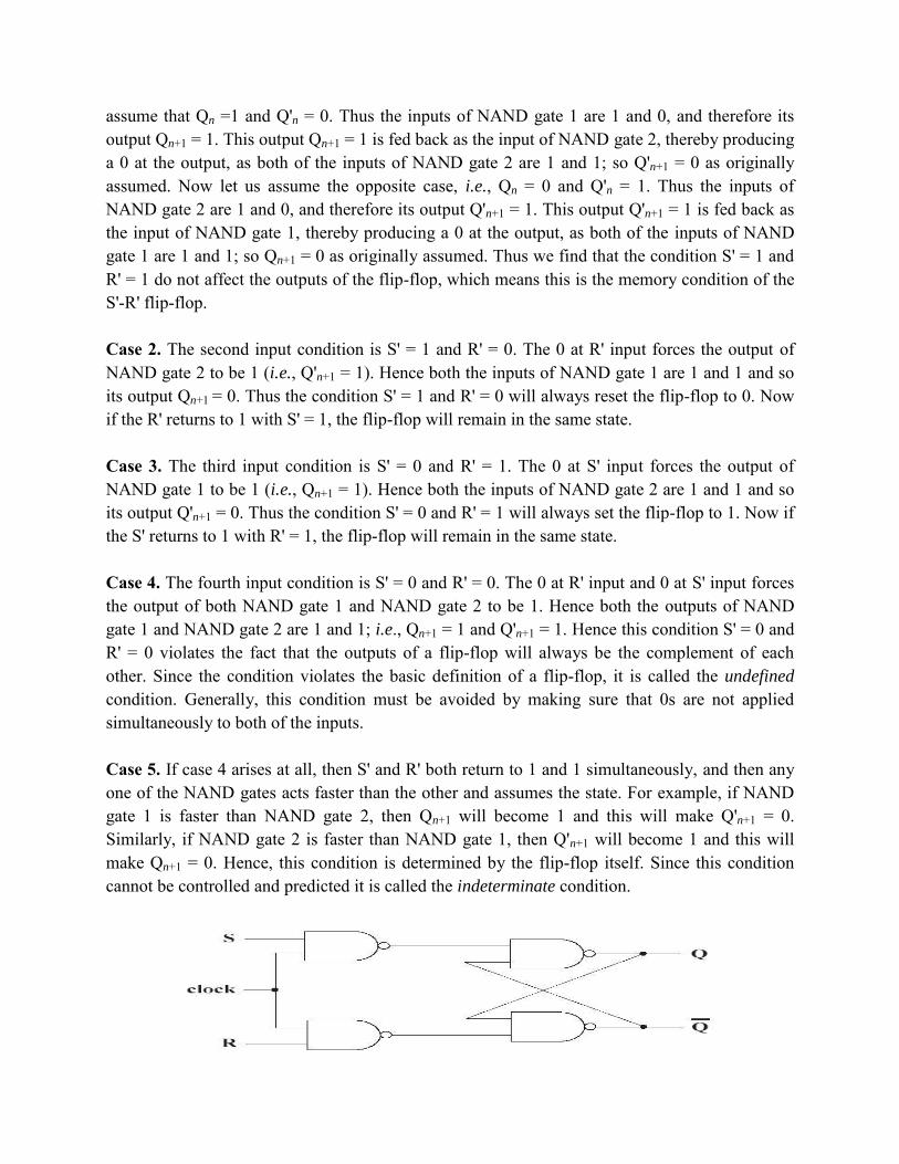
assume that Qn =1 and Q'n = 0. Thus the inputs of NAND gate 1 are 1 and 0, and therefore its output Qn+1 = 1. This output Qn+1 = 1 is fed back as the input of NAND gate 2, thereby producing a 0 at the output, as both of the inputs of NAND gate 2 are 1 and 1; so Q'n+1 = 0 as originally assumed. Now let us assume the opposite case, i.e., Qn = 0 and Q'n = 1. Thus the inputs of NAND gate 2 are 1 and 0, and therefore its output Q'n+1 = 1. This output Q'n+1 = 1 is fed back as the input of NAND gate 1, thereby producing a 0 at the output, as both of the inputs of NAND gate 1 are 1 and 1; so Qn+1 = 0 as originally assumed. Thus we find that the condition S' = 1 and R' = 1 do not affect the outputs of the flip-flop, which means this is the memory condition of the S'-R' flip-flop. Case 2. The second input condition is S' = 1 and R' = 0. The 0 at R' input forces the output of NAND gate 2 to be 1 (i.e., Q'n+1 = 1). Hence both the inputs of NAND gate 1 are 1 and 1 and so its output Qn+1 = 0. Thus the condition S' = 1 and R' = 0 will always reset the flip-flop to 0. Now if the R' returns to 1 with S' = 1, the flip-flop will remain in the same state. Case 3. The third input condition is S' = 0 and R' = 1. The 0 at S' input forces the output of NAND gate 1 to be 1 (i.e., Qn+1 = 1). Hence both the inputs of NAND gate 2 are 1 and 1 and so its output Q'n+1 = 0. Thus the condition S' = 0 and R' = 1 will always set the flip-flop to 1. Now if the S' returns to 1 with R' = 1, the flip-flop will remain in the same state. Case 4. The fourth input condition is S' = 0 and R' = 0. The 0 at R' input and 0 at S' input forces the output of both NAND gate 1 and NAND gate 2 to be 1. Hence both the outputs of NAND gate 1 and NAND gate 2 are 1 and 1; i.e., Qn+1 = 1 and Q'n+1 = 1. Hence this condition S' = 0 and R' = 0 violates the fact that the outputs of a flip-flop will always be the complement of each other. Since the condition violates the basic definition of a flip-flop, it is called the undefined
condition. Generally, this condition must be avoided by making sure that 0s are not applied simultaneously to both of the inputs. Case 5. If case 4 arises at all, then S' and R' both return to 1 and 1 simultaneously, and then any one of the NAND gates acts faster than the other and assumes the state. For example, if NAND gate 1 is faster than NAND gate 2, then Qn+1 will become 1 and this will make Q'n+1 = 0. Similarly, if NAND gate 2 is faster than NAND gate 1, then Q'n+1 will become 1 and this will make Qn+1 = 0. Hence, this condition is determined by the flip-flop itself. Since this condition cannot be controlled and predicted it is called the indeterminate condition.
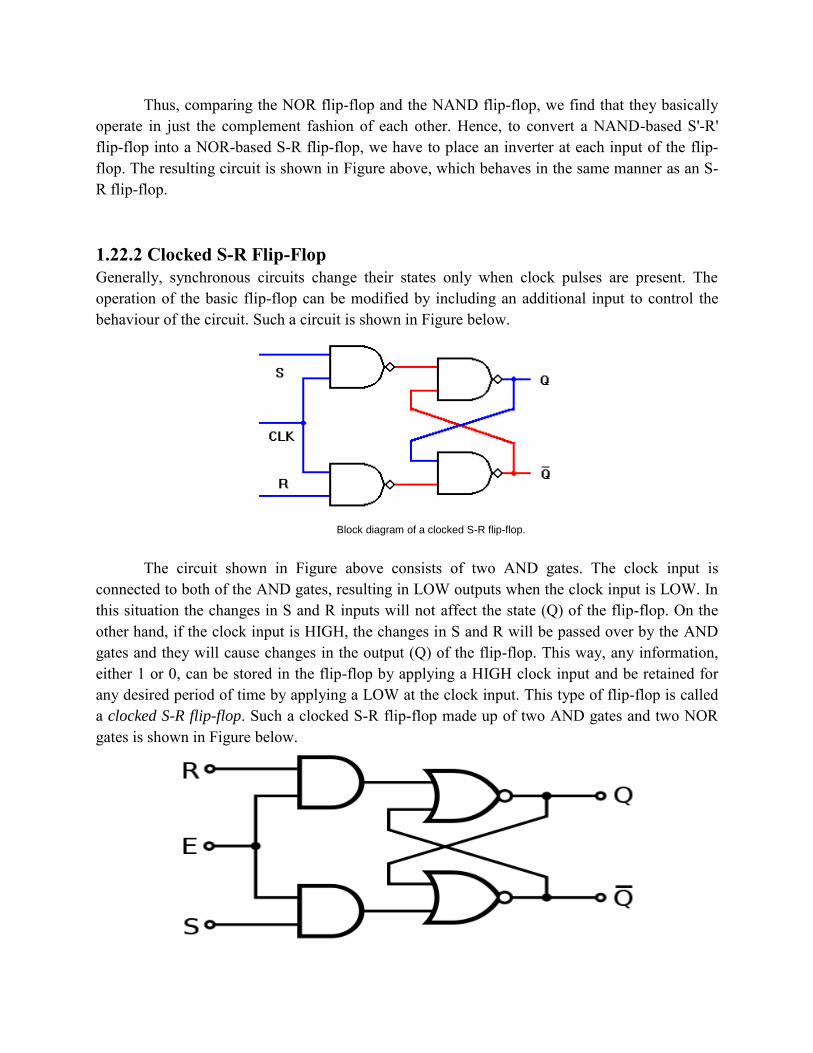
Thus, comparing the NOR flip-flop and the NAND flip-flop, we find that they basically operate in just the complement fashion of each other. Hence, to convert a NAND-based S'-R' flip-flop into a NOR-based S-R flip-flop, we have to place an inverter at each input of the flip-flop. The resulting circuit is shown in Figure above, which behaves in the same manner as an S-R flip-flop. 1.22.2 Clocked S-R Flip-Flop Generally, synchronous circuits change their states only when clock pulses are present. The operation of the basic flip-flop can be modified by including an additional input to control the behaviour of the circuit. Such a circuit is shown in Figure below.
Block diagram of a clocked S-R flip-flop.
The circuit shown in Figure above consists of two AND gates. The clock input is
connected to both of the AND gates, resulting in LOW outputs when the clock input is LOW. In this situation the changes in S and R inputs will not affect the state (Q) of the flip-flop. On the other hand, if the clock input is HIGH, the changes in S and R will be passed over by the AND gates and they will cause changes in the output (Q) of the flip-flop. This way, any information, either 1 or 0, can be stored in the flip-flop by applying a HIGH clock input and be retained for any desired period of time by applying a LOW at the clock input. This type of flip-flop is called a clocked S-R flip-flop. Such a clocked S-R flip-flop made up of two AND gates and two NOR gates is shown in Figure below.
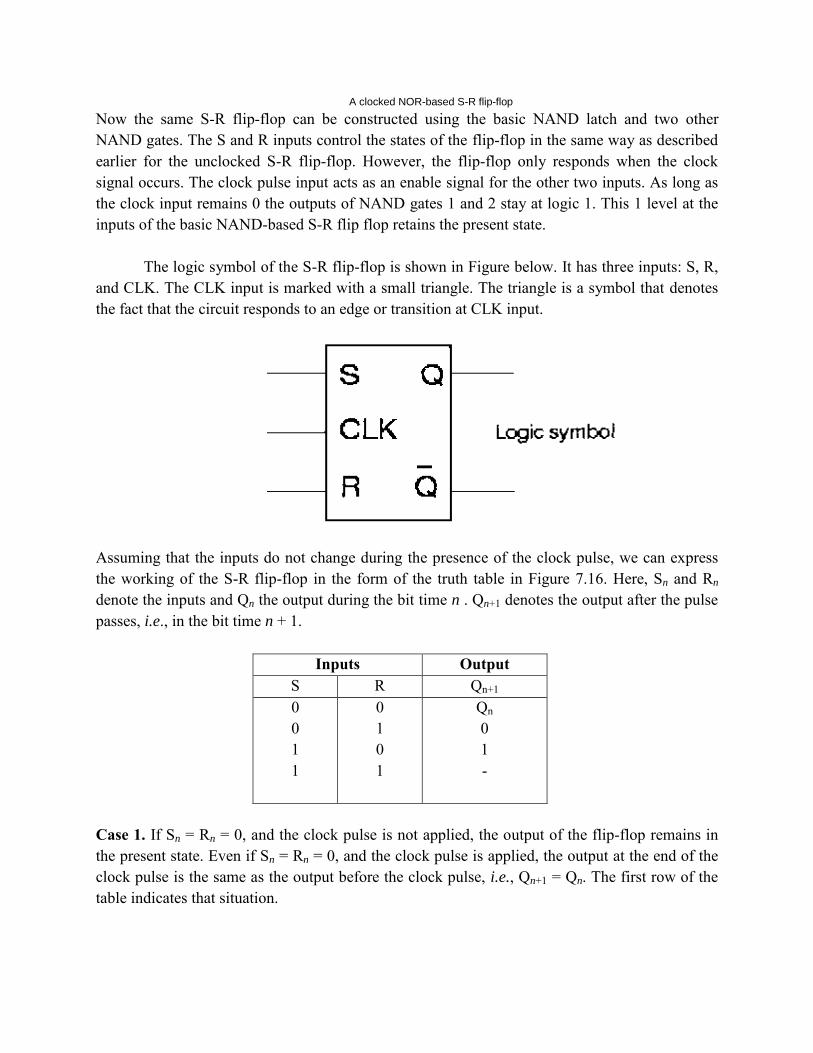
A clocked NOR-based S-R flip-flop Now the same S-R flip-flop can be constructed using the basic NAND latch and two other NAND gates. The S and R inputs control the states of the flip-flop in the same way as described earlier for the unclocked S-R flip-flop. However, the flip-flop only responds when the clock signal occurs. The clock pulse input acts as an enable signal for the other two inputs. As long as the clock input remains 0 the outputs of NAND gates 1 and 2 stay at logic 1. This 1 level at the inputs of the basic NAND-based S-R flip flop retains the present state. The logic symbol of the S-R flip-flop is shown in Figure below. It has three inputs: S, R, and CLK. The CLK input is marked with a small triangle. The triangle is a symbol that denotes the fact that the circuit responds to an edge or transition at CLK input.
Assuming that the inputs do not change during the presence of the clock pulse, we can express the working of the S-R flip-flop in the form of the truth table in Figure 7.16. Here, Sn and Rn
denote the inputs and Qn the output during the bit time n . Qn+1 denotes the output after the pulse passes, i.e., in the bit time n + 1.
Inputs Output S R Qn+1
0 0 1 1
0 1 0 1
Qn 0 1 -
Case 1. If Sn = Rn = 0, and the clock pulse is not applied, the output of the flip-flop remains in the present state. Even if Sn = Rn = 0, and the clock pulse is applied, the output at the end of the clock pulse is the same as the output before the clock pulse, i.e., Qn+1 = Qn. The first row of the table indicates that situation.
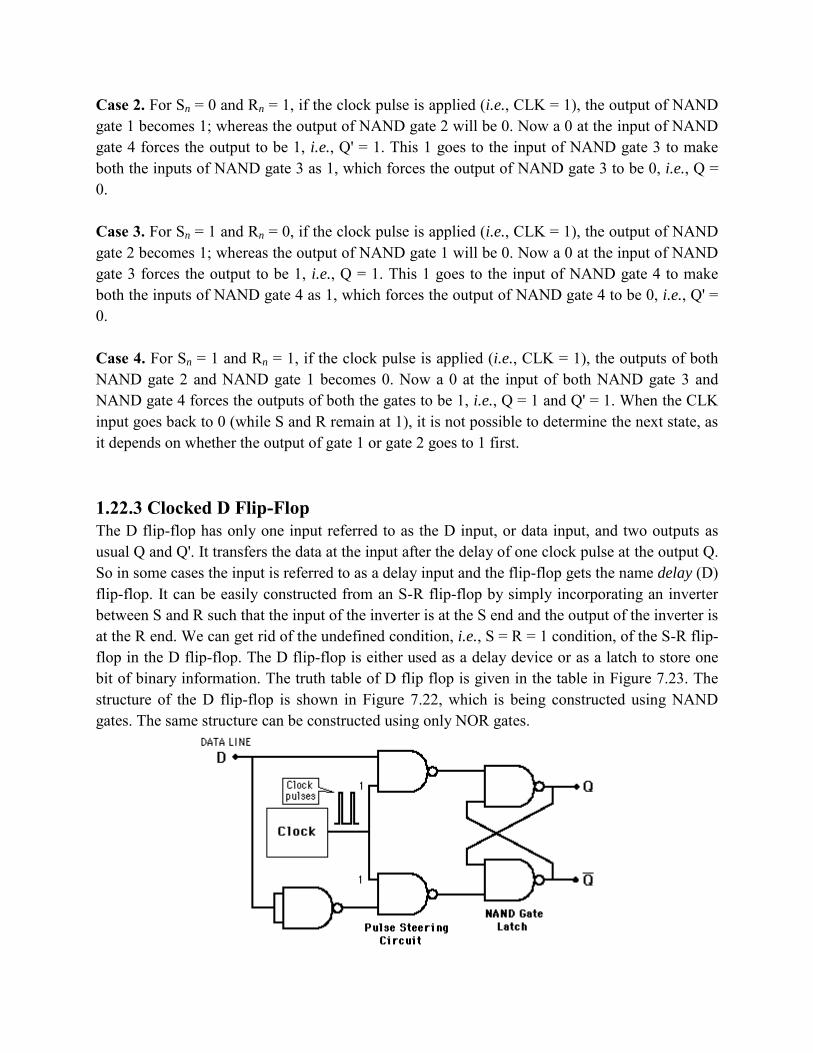
Case 2. For Sn = 0 and Rn = 1, if the clock pulse is applied (i.e., CLK = 1), the output of NAND gate 1 becomes 1; whereas the output of NAND gate 2 will be 0. Now a 0 at the input of NAND gate 4 forces the output to be 1, i.e., Q' = 1. This 1 goes to the input of NAND gate 3 to make both the inputs of NAND gate 3 as 1, which forces the output of NAND gate 3 to be 0, i.e., Q = 0. Case 3. For Sn = 1 and Rn = 0, if the clock pulse is applied (i.e., CLK = 1), the output of NAND gate 2 becomes 1; whereas the output of NAND gate 1 will be 0. Now a 0 at the input of NAND gate 3 forces the output to be 1, i.e., Q = 1. This 1 goes to the input of NAND gate 4 to make both the inputs of NAND gate 4 as 1, which forces the output of NAND gate 4 to be 0, i.e., Q' = 0. Case 4. For Sn = 1 and Rn = 1, if the clock pulse is applied (i.e., CLK = 1), the outputs of both NAND gate 2 and NAND gate 1 becomes 0. Now a 0 at the input of both NAND gate 3 and NAND gate 4 forces the outputs of both the gates to be 1, i.e., Q = 1 and Q' = 1. When the CLK input goes back to 0 (while S and R remain at 1), it is not possible to determine the next state, as it depends on whether the output of gate 1 or gate 2 goes to 1 first. 1.22.3 Clocked D Flip-Flop The D flip-flop has only one input referred to as the D input, or data input, and two outputs as usual Q and Q'. It transfers the data at the input after the delay of one clock pulse at the output Q. So in some cases the input is referred to as a delay input and the flip-flop gets the name delay (D) flip-flop. It can be easily constructed from an S-R flip-flop by simply incorporating an inverter between S and R such that the input of the inverter is at the S end and the output of the inverter is at the R end. We can get rid of the undefined condition, i.e., S = R = 1 condition, of the S-R flip-flop in the D flip-flop. The D flip-flop is either used as a delay device or as a latch to store one bit of binary information. The truth table of D flip flop is given in the table in Figure 7.23. The structure of the D flip-flop is shown in Figure 7.22, which is being constructed using NAND gates. The same structure can be constructed using only NOR gates.
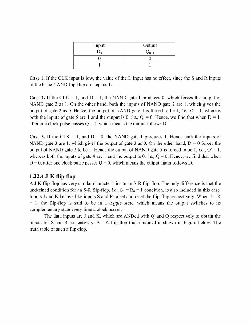
Input Dn
Output Qn+1
0 1
0 1
Case 1. If the CLK input is low, the value of the D input has no effect, since the S and R inputs of the basic NAND flip-flop are kept as 1. Case 2. If the CLK = 1, and D = 1, the NAND gate 1 produces 0, which forces the output of NAND gate 3 as 1. On the other hand, both the inputs of NAND gate 2 are 1, which gives the output of gate 2 as 0. Hence, the output of NAND gate 4 is forced to be 1, i.e., Q = 1, whereas both the inputs of gate 5 are 1 and the output is 0, i.e., Q' = 0. Hence, we find that when D = 1, after one clock pulse passes Q = 1, which means the output follows D. Case 3. If the CLK = 1, and D = 0, the NAND gate 1 produces 1. Hence both the inputs of NAND gate 3 are 1, which gives the output of gate 3 as 0. On the other hand, D = 0 forces the output of NAND gate 2 to be 1. Hence the output of NAND gate 5 is forced to be 1, i.e., Q' = 1, whereas both the inputs of gate 4 are 1 and the output is 0, i.e., Q = 0. Hence, we find that when D = 0, after one clock pulse passes Q = 0, which means the output again follows D. 1.22.4 J-K flip-flop A J-K flip-flop has very similar characteristics to an S-R flip-flop. The only difference is that the undefined condition for an S-R flip-flop, i.e., Sn = Rn = 1 condition, is also included in this case. Inputs J and K behave like inputs S and R to set and reset the flip-flop respectively. When J = K = 1, the flip-flop is said to be in a toggle state, which means the output switches to its complementary state every time a clock passes.
The data inputs are J and K, which are ANDed with Q' and Q respectively to obtain the inputs for S and R respectively. A J-K flip-flop thus obtained is shown in Figure below. The truth table of such a flip-flop.
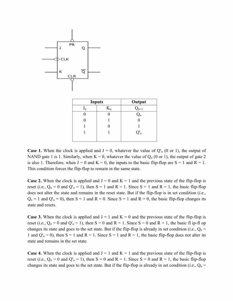
Inputs Output Jn Kn Qn+1
0 0 1 1
0 1 0 1
Qn 0 1
Q'n
Case 1. When the clock is applied and J = 0, whatever the value of Q'n (0 or 1), the output of NAND gate 1 is 1. Similarly, when K = 0, whatever the value of Qn (0 or 1), the output of gate 2 is also 1. Therefore, when J = 0 and K = 0, the inputs to the basic flip-flop are S = 1 and R = 1. This condition forces the flip-flop to remain in the same state. Case 2. When the clock is applied and J = 0 and K = 1 and the previous state of the flip-flop is reset (i.e., Qn = 0 and Q'n = 1), then S = 1 and R = 1. Since S = 1 and R = 1, the basic flip-flop does not alter the state and remains in the reset state. But if the flip-flop is in set condition (i.e., Qn = 1 and Q'n = 0), then S = 1 and R = 0. Since S = 1 and R = 0, the basic flip-flop changes its state and resets. Case 3. When the clock is applied and J = 1 and K = 0 and the previous state of the flip-flop is reset (i.e., Qn = 0 and Q'n = 1), then S = 0 and R = 1. Since S = 0 and R = 1, the basic fl ip-fl op changes its state and goes to the set state. But if the flip-flop is already in set condition (i.e., Qn = 1 and Q'n = 0), then S = 1 and R = 1. Since S = 1 and R = 1, the basic flip-flop does not alter its state and remains in the set state. Case 4. When the clock is applied and J = 1 and K = 1 and the previous state of the flip-flop is reset (i.e., Qn = 0 and Q'n = 1), then S = 0 and R = 1. Since S = 0 and R = 1, the basic flip-flop changes its state and goes to the set state. But if the flip-flop is already in set condition (i.e., Qn =
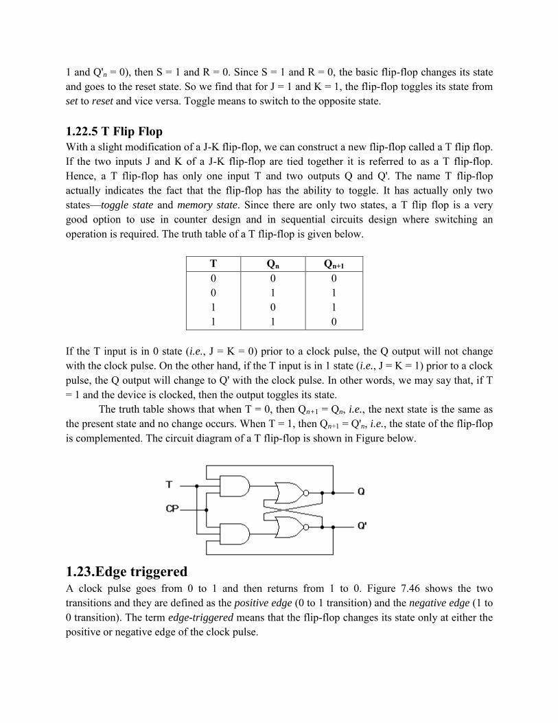
1 and Q'n = 0), then S = 1 and R = 0. Since S = 1 and R = 0, the basic flip-flop changes its state and goes to the reset state. So we find that for J = 1 and K = 1, the flip-flop toggles its state from set to reset and vice versa. Toggle means to switch to the opposite state. 1.22.5 T Flip Flop With a slight modification of a J-K flip-flop, we can construct a new flip-flop called a T flip flop. If the two inputs J and K of a J-K flip-flop are tied together it is referred to as a T flip-flop. Hence, a T flip-flop has only one input T and two outputs Q and Q'. The name T flip-flop actually indicates the fact that the flip-flop has the ability to toggle. It has actually only two states—toggle state and memory state. Since there are only two states, a T flip flop is a very good option to use in counter design and in sequential circuits design where switching an operation is required. The truth table of a T flip-flop is given below.
T Qn Qn+1
0 0 1 1
0 1 0 1
0 1 1 0
If the T input is in 0 state (i.e., J = K = 0) prior to a clock pulse, the Q output will not change with the clock pulse. On the other hand, if the T input is in 1 state (i.e., J = K = 1) prior to a clock pulse, the Q output will change to Q' with the clock pulse. In other words, we may say that, if T = 1 and the device is clocked, then the output toggles its state.
The truth table shows that when T = 0, then Qn+1 = Qn, i.e., the next state is the same as the present state and no change occurs. When T = 1, then Qn+1 = Q'n, i.e., the state of the flip-flop is complemented. The circuit diagram of a T flip-flop is shown in Figure below.
1.23.Edge triggered A clock pulse goes from 0 to 1 and then returns from 1 to 0. Figure 7.46 shows the two transitions and they are defined as the positive edge (0 to 1 transition) and the negative edge (1 to 0 transition). The term edge-triggered means that the flip-flop changes its state only at either the positive or negative edge of the clock pulse.
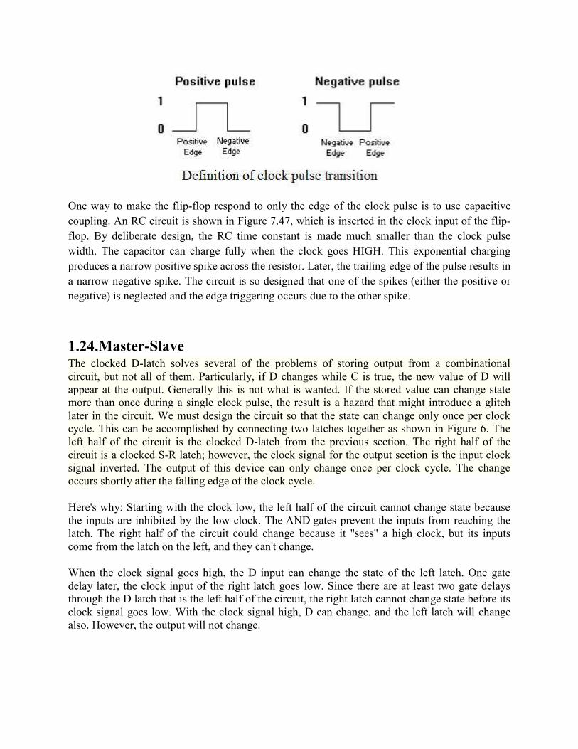
One way to make the flip-flop respond to only the edge of the clock pulse is to use capacitive coupling. An RC circuit is shown in Figure 7.47, which is inserted in the clock input of the flip-flop. By deliberate design, the RC time constant is made much smaller than the clock pulse width. The capacitor can charge fully when the clock goes HIGH. This exponential charging produces a narrow positive spike across the resistor. Later, the trailing edge of the pulse results in a narrow negative spike. The circuit is so designed that one of the spikes (either the positive or negative) is neglected and the edge triggering occurs due to the other spike. 1.24.Master-Slave The clocked D-latch solves several of the problems of storing output from a combinational circuit, but not all of them. Particularly, if D changes while C is true, the new value of D will appear at the output. Generally this is not what is wanted. If the stored value can change state more than once during a single clock pulse, the result is a hazard that might introduce a glitch later in the circuit. We must design the circuit so that the state can change only once per clock cycle. This can be accomplished by connecting two latches together as shown in Figure 6. The left half of the circuit is the clocked D-latch from the previous section. The right half of the circuit is a clocked S-R latch; however, the clock signal for the output section is the input clock signal inverted. The output of this device can only change once per clock cycle. The change occurs shortly after the falling edge of the clock cycle.
Here's why: Starting with the clock low, the left half of the circuit cannot change state because the inputs are inhibited by the low clock. The AND gates prevent the inputs from reaching the latch. The right half of the circuit could change because it "sees" a high clock, but its inputs come from the latch on the left, and they can't change.
When the clock signal goes high, the D input can change the state of the left latch. One gate delay later, the clock input of the right latch goes low. Since there are at least two gate delays through the D latch that is the left half of the circuit, the right latch cannot change state before its clock signal goes low. With the clock signal high, D can change, and the left latch will change also. However, the output will not change.
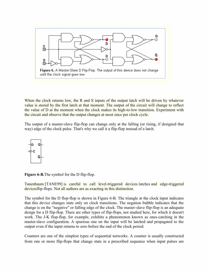
When the clock returns low, the R and S inputs of the output latch will be driven by whatever value is stored by the first latch at that moment. The output of the circuit will change to reflect the value of D at the moment when the clock makes its high-to-low transition. Experiment with the circuit and observe that the output changes at most once per clock cycle.
The output of a master-slave flip-flop can change only at the falling (or rising, if designed that way) edge of the clock pulse. That's why we call it a flip-flop instead of a latch.
Figure 6-B.The symbol for the D flip-flop.
Tanenbaum [TANE99] is careful to call level-triggered devices latches and edge-triggered devicesflip-flops. Not all authors are as exacting in this distinction.
The symbol for the D flop-flop is shown in Figure 6-B. The triangle at the clock input indicates that this device changes state only on clock transitions. The negation bubble indicates that the change is on the "negative" or falling edge of the clock. The master-slave flip-flop is an adequate design for a D flip-flop. There are other types of flip-flops, not studied here, for which it doesn't work. The J-K flop-flop, for example, exhibits a phenomenon known as ones-catching in the master-slave configuration. A spurious one on the input will be latched and propagated to the output even if the input returns to zero before the end of the clock period.
Counters are one of the simplest types of sequential networks. A counter is usually constructed from one or more flip-flops that change state in a prescribed sequence when input pulses are
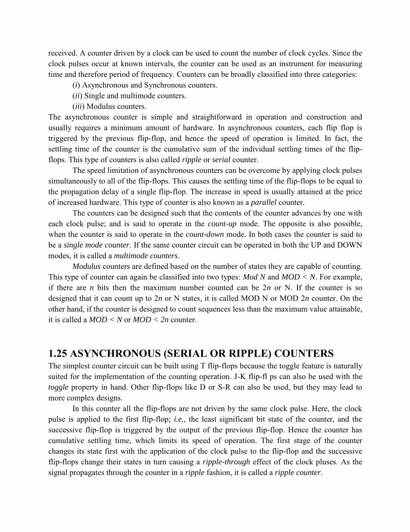
received. A counter driven by a clock can be used to count the number of clock cycles. Since the clock pulses occur at known intervals, the counter can be used as an instrument for measuring time and therefore period of frequency. Counters can be broadly classified into three categories:
(i) Asynchronous and Synchronous counters. (ii) Single and multimode counters. (iii) Modulus counters.
The asynchronous counter is simple and straightforward in operation and construction and usually requires a minimum amount of hardware. In asynchronous counters, each flip flop is triggered by the previous flip-flop, and hence the speed of operation is limited. In fact, the settling time of the counter is the cumulative sum of the individual settling times of the flip-flops. This type of counters is also called ripple or serial counter.
The speed limitation of asynchronous counters can be overcome by applying clock pulses simultaneously to all of the flip-flops. This causes the settling time of the flip-flops to be equal to the propagation delay of a single flip-flop. The increase in speed is usually attained at the price of increased hardware. This type of counter is also known as a parallel counter.
The counters can be designed such that the contents of the counter advances by one with each clock pulse; and is said to operate in the count-up mode. The opposite is also possible, when the counter is said to operate in the count-down mode. In both cases the counter is said to be a single mode counter. If the same counter circuit can be operated in both the UP and DOWN modes, it is called a multimode counters.
Modulus counters are defined based on the number of states they are capable of counting. This type of counter can again be classified into two types: Mod N and MOD < N. For example, if there are n bits then the maximum number counted can be 2n or N. If the counter is so designed that it can count up to 2n or N states, it is called MOD N or MOD 2n counter. On the other hand, if the counter is designed to count sequences less than the maximum value attainable, it is called a MOD < N or MOD < 2n counter.
1.25 ASYNCHRONOUS (SERIAL OR RIPPLE) COUNTERS The simplest counter circuit can be built using T flip-flops because the toggle feature is naturally suited for the implementation of the counting operation. J-K flip-fl ps can also be used with the toggle property in hand. Other flip-flops like D or S-R can also be used, but they may lead to more complex designs.
In this counter all the flip-flops are not driven by the same clock pulse. Here, the clock pulse is applied to the first flip-flop; i.e., the least significant bit state of the counter, and the successive flip-flop is triggered by the output of the previous flip-flop. Hence the counter has cumulative settling time, which limits its speed of operation. The first stage of the counter changes its state first with the application of the clock pulse to the flip-flop and the successive flip-flops change their states in turn causing a ripple-through effect of the clock pluses. As the signal propagates through the counter in a ripple fashion, it is called a ripple counter.
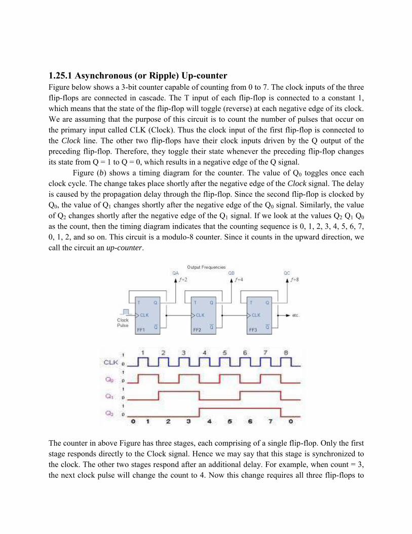
1.25.1 Asynchronous (or Ripple) Up-counter Figure below shows a 3-bit counter capable of counting from 0 to 7. The clock inputs of the three flip-flops are connected in cascade. The T input of each flip-flop is connected to a constant 1, which means that the state of the flip-flop will toggle (reverse) at each negative edge of its clock. We are assuming that the purpose of this circuit is to count the number of pulses that occur on the primary input called CLK (Clock). Thus the clock input of the first flip-flop is connected to the Clock line. The other two flip-flops have their clock inputs driven by the Q output of the preceding flip-flop. Therefore, they toggle their state whenever the preceding flip-flop changes its state from Q = 1 to Q = 0, which results in a negative edge of the Q signal.
Figure (b) shows a timing diagram for the counter. The value of Q0 toggles once each clock cycle. The change takes place shortly after the negative edge of the Clock signal. The delay is caused by the propagation delay through the flip-flop. Since the second flip-flop is clocked by Q0, the value of Q1 changes shortly after the negative edge of the Q0 signal. Similarly, the value of Q2 changes shortly after the negative edge of the Q1 signal. If we look at the values Q2 Q1 Q0 as the count, then the timing diagram indicates that the counting sequence is 0, 1, 2, 3, 4, 5, 6, 7, 0, 1, 2, and so on. This circuit is a modulo-8 counter. Since it counts in the upward direction, we call the circuit an up-counter.
The counter in above Figure has three stages, each comprising of a single flip-flop. Only the first stage responds directly to the Clock signal. Hence we may say that this stage is synchronized to the clock. The other two stages respond after an additional delay. For example, when count = 3, the next clock pulse will change the count to 4. Now this change requires all three flip-flops to
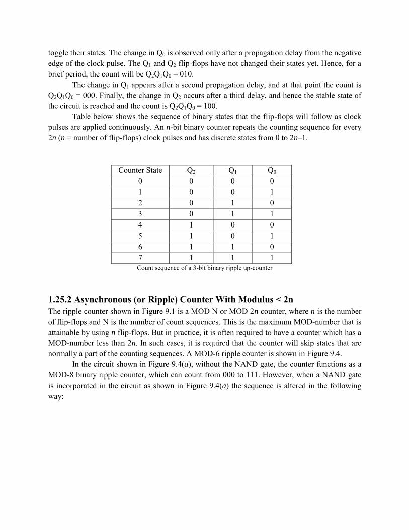
toggle their states. The change in Q0 is observed only after a propagation delay from the negative edge of the clock pulse. The Q1 and Q2 flip-flops have not changed their states yet. Hence, for a brief period, the count will be Q2Q1Q0 = 010.
The change in Q1 appears after a second propagation delay, and at that point the count is Q2Q1Q0 = 000. Finally, the change in Q2 occurs after a third delay, and hence the stable state of the circuit is reached and the count is Q2Q1Q0 = 100.
Table below shows the sequence of binary states that the flip-flops will follow as clock pulses are applied continuously. An n-bit binary counter repeats the counting sequence for every 2n (n = number of flip-flops) clock pulses and has discrete states from 0 to 2n–1.
Counter State Q2 Q1 Q0
0 0 0 0 1 0 0 1 2 0 1 0 3 0 1 1 4 1 0 0 5 1 0 1 6 1 1 0 7 1 1 1 Count sequence of a 3-bit binary ripple up-counter
1.25.2 Asynchronous (or Ripple) Counter With Modulus < 2n The ripple counter shown in Figure 9.1 is a MOD N or MOD 2n counter, where n is the number of flip-flops and N is the number of count sequences. This is the maximum MOD-number that is attainable by using n flip-flops. But in practice, it is often required to have a counter which has a MOD-number less than 2n. In such cases, it is required that the counter will skip states that are normally a part of the counting sequences. A MOD-6 ripple counter is shown in Figure 9.4.
In the circuit shown in Figure 9.4(a), without the NAND gate, the counter functions as a MOD-8 binary ripple counter, which can count from 000 to 111. However, when a NAND gate is incorporated in the circuit as shown in Figure 9.4(a) the sequence is altered in the following way:
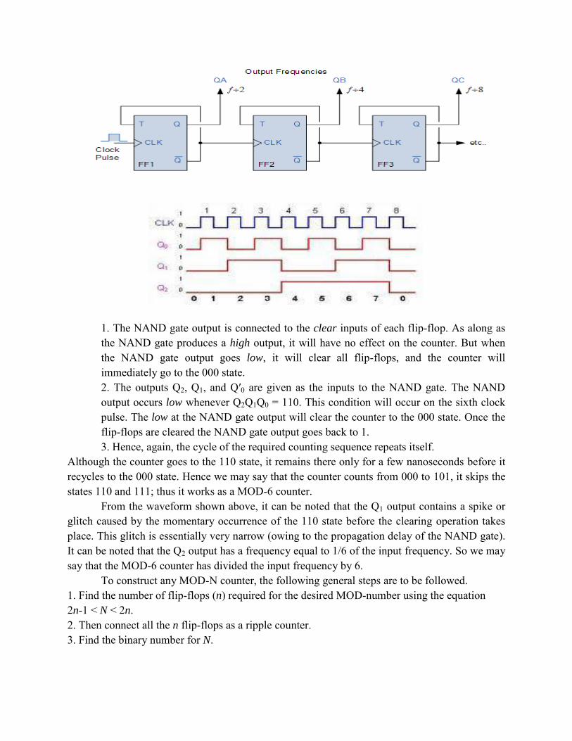
1. The NAND gate output is connected to the clear inputs of each flip-flop. As along as the NAND gate produces a high output, it will have no effect on the counter. But when the NAND gate output goes low, it will clear all flip-flops, and the counter will immediately go to the 000 state. 2. The outputs Q2, Q1, and Q′0 are given as the inputs to the NAND gate. The NAND output occurs low whenever Q2Q1Q0 = 110. This condition will occur on the sixth clock pulse. The low at the NAND gate output will clear the counter to the 000 state. Once the flip-flops are cleared the NAND gate output goes back to 1. 3. Hence, again, the cycle of the required counting sequence repeats itself.
Although the counter goes to the 110 state, it remains there only for a few nanoseconds before it recycles to the 000 state. Hence we may say that the counter counts from 000 to 101, it skips the states 110 and 111; thus it works as a MOD-6 counter.
From the waveform shown above, it can be noted that the Q1 output contains a spike or glitch caused by the momentary occurrence of the 110 state before the clearing operation takes place. This glitch is essentially very narrow (owing to the propagation delay of the NAND gate). It can be noted that the Q2 output has a frequency equal to 1/6 of the input frequency. So we may say that the MOD-6 counter has divided the input frequency by 6.
To construct any MOD-N counter, the following general steps are to be followed. 1. Find the number of flip-flops (n) required for the desired MOD-number using the equation 2n-1 < N < 2n. 2. Then connect all the n flip-flops as a ripple counter. 3. Find the binary number for N.
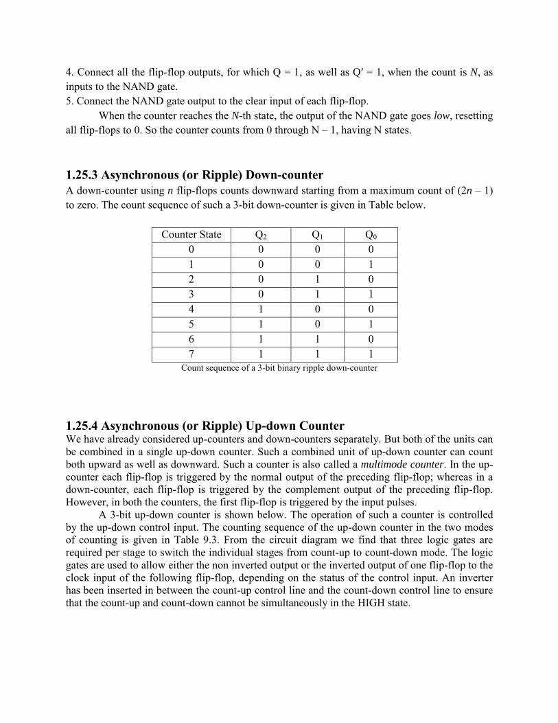
4. Connect all the flip-flop outputs, for which Q = 1, as well as Q′ = 1, when the count is N, as inputs to the NAND gate. 5. Connect the NAND gate output to the clear input of each flip-flop.
When the counter reaches the N-th state, the output of the NAND gate goes low, resetting all flip-flops to 0. So the counter counts from 0 through N – 1, having N states. 1.25.3 Asynchronous (or Ripple) Down-counter A down-counter using n flip-flops counts downward starting from a maximum count of (2n – 1) to zero. The count sequence of such a 3-bit down-counter is given in Table below.
Counter State Q2 Q1 Q0
0 0 0 0 1 0 0 1 2 0 1 0 3 0 1 1 4 1 0 0 5 1 0 1 6 1 1 0 7 1 1 1
Count sequence of a 3-bit binary ripple down-counter 1.25.4 Asynchronous (or Ripple) Up-down Counter We have already considered up-counters and down-counters separately. But both of the units can be combined in a single up-down counter. Such a combined unit of up-down counter can count both upward as well as downward. Such a counter is also called a multimode counter. In the up-counter each flip-flop is triggered by the normal output of the preceding flip-flop; whereas in a down-counter, each flip-flop is triggered by the complement output of the preceding flip-flop. However, in both the counters, the first flip-flop is triggered by the input pulses.
A 3-bit up-down counter is shown below. The operation of such a counter is controlled by the up-down control input. The counting sequence of the up-down counter in the two modes of counting is given in Table 9.3. From the circuit diagram we find that three logic gates are required per stage to switch the individual stages from count-up to count-down mode. The logic gates are used to allow either the non inverted output or the inverted output of one flip-flop to the clock input of the following flip-flop, depending on the status of the control input. An inverter has been inserted in between the count-up control line and the count-down control line to ensure that the count-up and count-down cannot be simultaneously in the HIGH state.
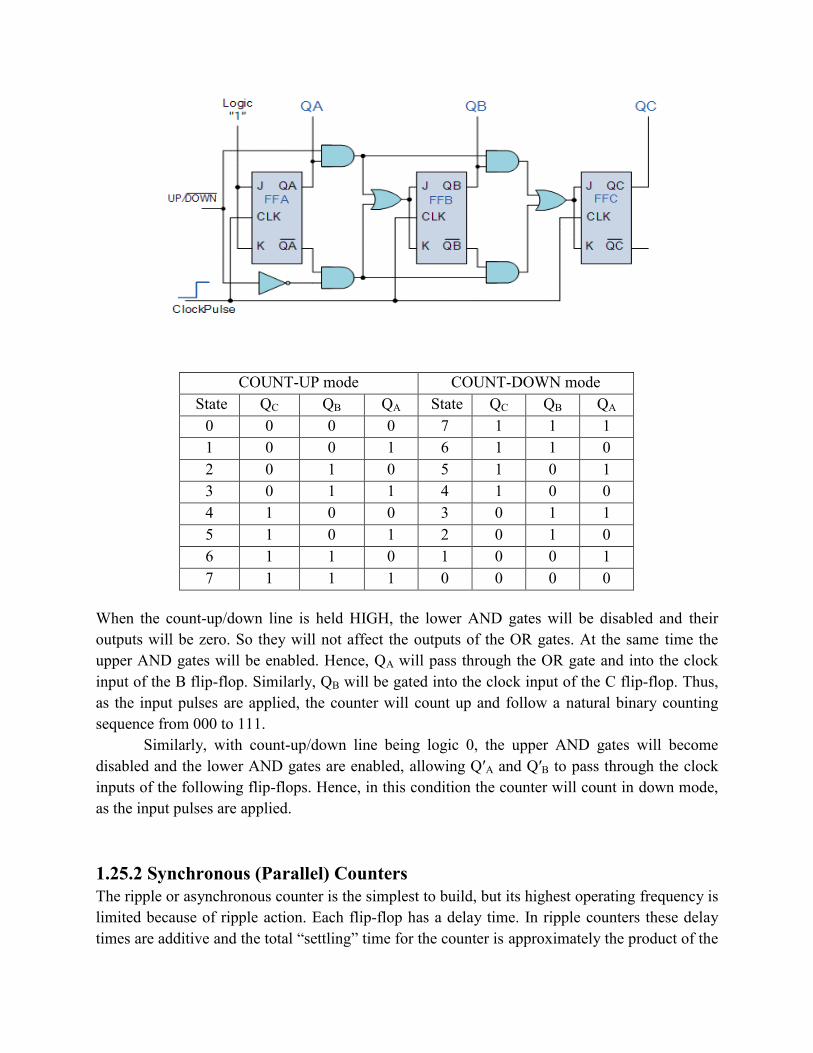
COUNT-UP mode COUNT-DOWN mode
State QC QB QA State QC QB QA
0 0 0 0 7 1 1 1 1 0 0 1 6 1 1 0 2 0 1 0 5 1 0 1 3 0 1 1 4 1 0 0 4 1 0 0 3 0 1 1 5 1 0 1 2 0 1 0 6 1 1 0 1 0 0 1 7 1 1 1 0 0 0 0
When the count-up/down line is held HIGH, the lower AND gates will be disabled and their outputs will be zero. So they will not affect the outputs of the OR gates. At the same time the upper AND gates will be enabled. Hence, QA will pass through the OR gate and into the clock input of the B flip-flop. Similarly, QB will be gated into the clock input of the C flip-flop. Thus, as the input pulses are applied, the counter will count up and follow a natural binary counting sequence from 000 to 111.
Similarly, with count-up/down line being logic 0, the upper AND gates will become disabled and the lower AND gates are enabled, allowing Q′A and Q′B to pass through the clock inputs of the following flip-flops. Hence, in this condition the counter will count in down mode, as the input pulses are applied. 1.25.2 Synchronous (Parallel) Counters The ripple or asynchronous counter is the simplest to build, but its highest operating frequency is limited because of ripple action. Each flip-flop has a delay time. In ripple counters these delay times are additive and the total ―settling‖ time for the counter is approximately the product of the
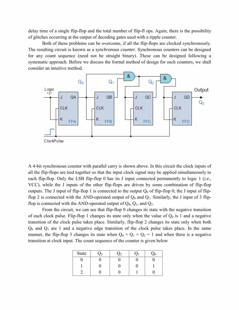
delay time of a single flip-flop and the total number of flip-fl ops. Again, there is the possibility of glitches occurring at the output of decoding gates used with a ripple counter.
Both of these problems can be overcome, if all the flip-flops are clocked synchronously. The resulting circuit is known as a synchronous counter. Synchronous counters can be designed for any count sequence (need not be straight binary). These can be designed following a systematic approach. Before we discuss the formal method of design for such counters, we shall consider an intuitive method.
A 4-bit synchronous counter with parallel carry is shown above. In this circuit the clock inputs of all the flip-flops are tied together so that the input clock signal may be applied simultaneously to each flip-flop. Only the LSB flip-flop 0 has its J input connected permanently to logic 1 (i.e., VCC), while the J inputs of the other flip-flops are driven by some combination of flip-flop outputs. The J input of flip-flop 1 is connected to the output Q0 of flip-flop 0; the J input of flip-flop 2 is connected with the AND-operated output of Q0 and Q1. Similarly, the J input of 3 flip-flop is connected with the AND-operated output of Q0, Q1, and Q2.
From the circuit, we can see that flip-flop 0 changes its state with the negative transition of each clock pulse. Flip-flop 1 changes its state only when the value of Q0 is 1 and a negative transition of the clock pulse takes place. Similarly, flip-flop 2 changes its state only when both Q0 and Q1 are 1 and a negative edge transition of the clock pulse takes place. In the same manner, the flip-flop 3 changes its state when Q0 = Q1 = Q2 = 1 and when there is a negative transition at clock input. The count sequence of the counter is given below
State Q3 Q2 Q1 Q0
0 1 2
0 0 0
0 0 0
0 0 1
0 1 0
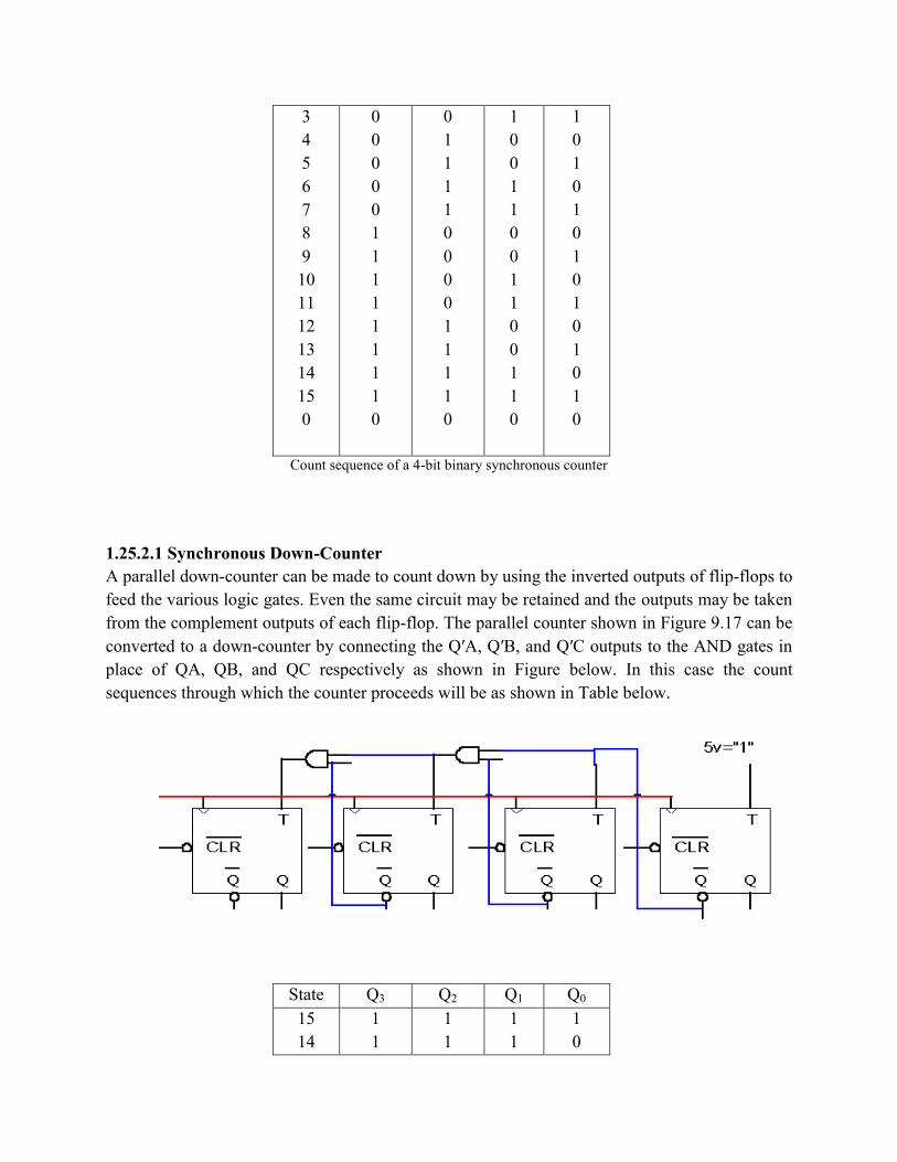
3 4 5 6 7 8 9 10 11 12 13 14 15 0
0 0 0 0 0 1 1 1 1 1 1 1 1 0
0 1 1 1 1 0 0 0 0 1 1 1 1 0
1 0 0 1 1 0 0 1 1 0 0 1 1 0
1 0 1 0 1 0 1 0 1 0 1 0 1 0
Count sequence of a 4-bit binary synchronous counter
1.25.2.1 Synchronous Down-Counter A parallel down-counter can be made to count down by using the inverted outputs of flip-flops to feed the various logic gates. Even the same circuit may be retained and the outputs may be taken from the complement outputs of each flip-flop. The parallel counter shown in Figure 9.17 can be converted to a down-counter by connecting the Q′A, Q′B, and Q′C outputs to the AND gates in place of QA, QB, and QC respectively as shown in Figure below. In this case the count sequences through which the counter proceeds will be as shown in Table below.
State Q3 Q2 Q1 Q0
15 14
1 1
1 1
1 1
1 0
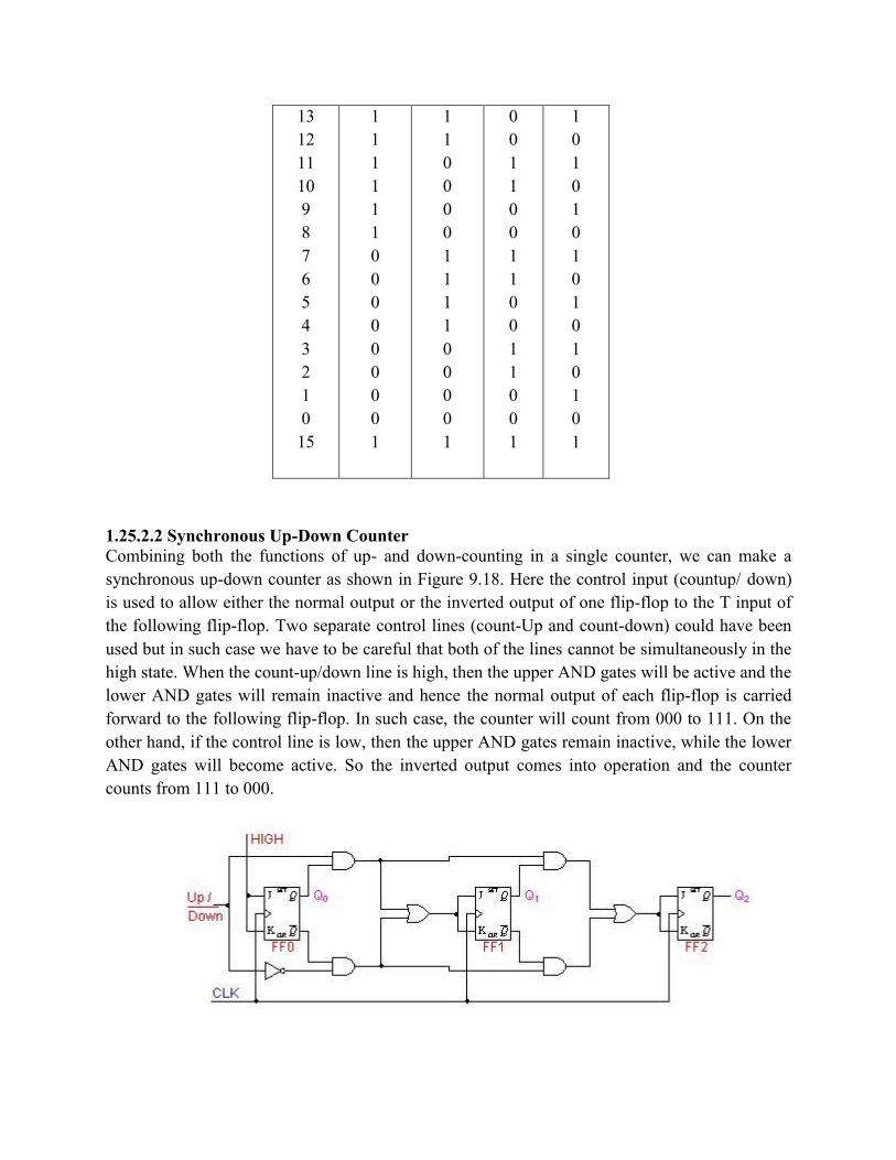
13 12 11 10 9 8 7 6 5 4 3 2 1 0 15
1 1 1 1 1 1 0 0 0 0 0 0 0 0 1
1 1 0 0 0 0 1 1 1 1 0 0 0 0 1
0 0 1 1 0 0 1 1 0 0 1 1 0 0 1
1 0 1 0 1 0 1 0 1 0 1 0 1 0 1
1.25.2.2 Synchronous Up-Down Counter Combining both the functions of up- and down-counting in a single counter, we can make a synchronous up-down counter as shown in Figure 9.18. Here the control input (countup/ down) is used to allow either the normal output or the inverted output of one flip-flop to the T input of the following flip-flop. Two separate control lines (count-Up and count-down) could have been used but in such case we have to be careful that both of the lines cannot be simultaneously in the high state. When the count-up/down line is high, then the upper AND gates will be active and the lower AND gates will remain inactive and hence the normal output of each flip-flop is carried forward to the following flip-flop. In such case, the counter will count from 000 to 111. On the other hand, if the control line is low, then the upper AND gates remain inactive, while the lower AND gates will become active. So the inverted output comes into operation and the counter counts from 111 to 000.
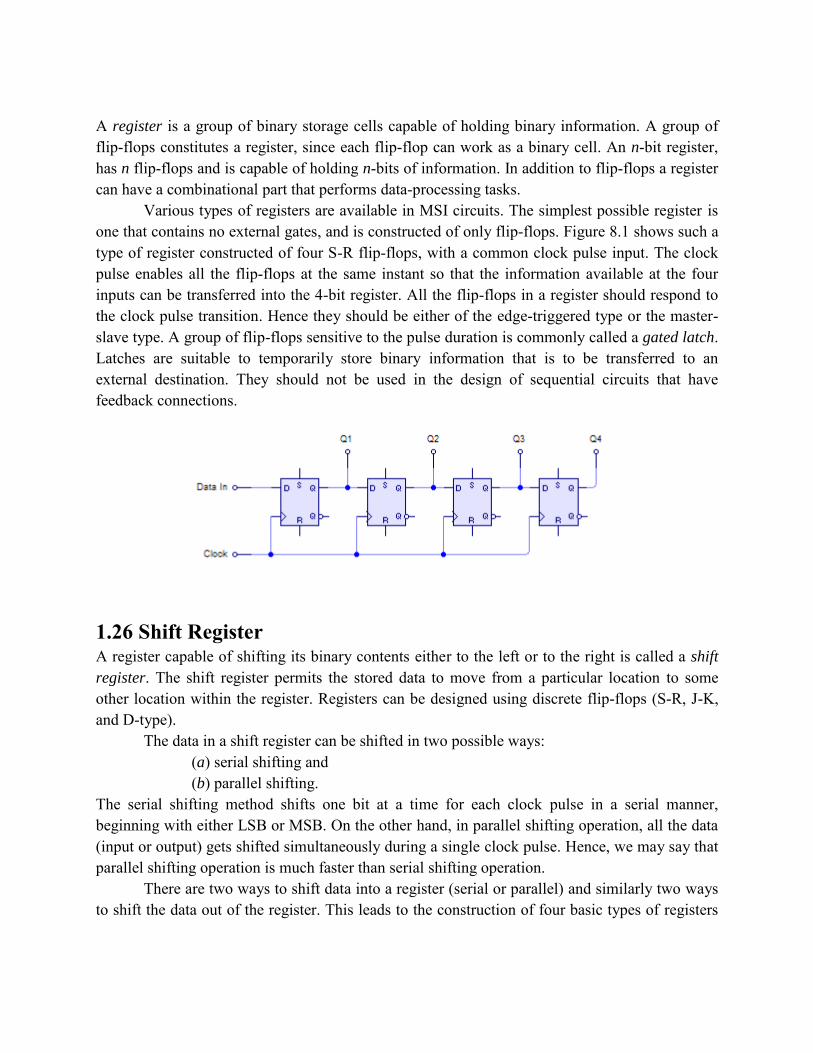
A register is a group of binary storage cells capable of holding binary information. A group of flip-flops constitutes a register, since each flip-flop can work as a binary cell. An n-bit register, has n flip-flops and is capable of holding n-bits of information. In addition to flip-flops a register can have a combinational part that performs data-processing tasks.
Various types of registers are available in MSI circuits. The simplest possible register is one that contains no external gates, and is constructed of only flip-flops. Figure 8.1 shows such a type of register constructed of four S-R flip-flops, with a common clock pulse input. The clock pulse enables all the flip-flops at the same instant so that the information available at the four inputs can be transferred into the 4-bit register. All the flip-flops in a register should respond to the clock pulse transition. Hence they should be either of the edge-triggered type or the master-slave type. A group of flip-flops sensitive to the pulse duration is commonly called a gated latch. Latches are suitable to temporarily store binary information that is to be transferred to an external destination. They should not be used in the design of sequential circuits that have feedback connections.
1.26 Shift Register A register capable of shifting its binary contents either to the left or to the right is called a shift
register. The shift register permits the stored data to move from a particular location to some other location within the register. Registers can be designed using discrete flip-flops (S-R, J-K, and D-type).
The data in a shift register can be shifted in two possible ways: (a) serial shifting and (b) parallel shifting.
The serial shifting method shifts one bit at a time for each clock pulse in a serial manner, beginning with either LSB or MSB. On the other hand, in parallel shifting operation, all the data (input or output) gets shifted simultaneously during a single clock pulse. Hence, we may say that parallel shifting operation is much faster than serial shifting operation.
There are two ways to shift data into a register (serial or parallel) and similarly two ways to shift the data out of the register. This leads to the construction of four basic types of registers
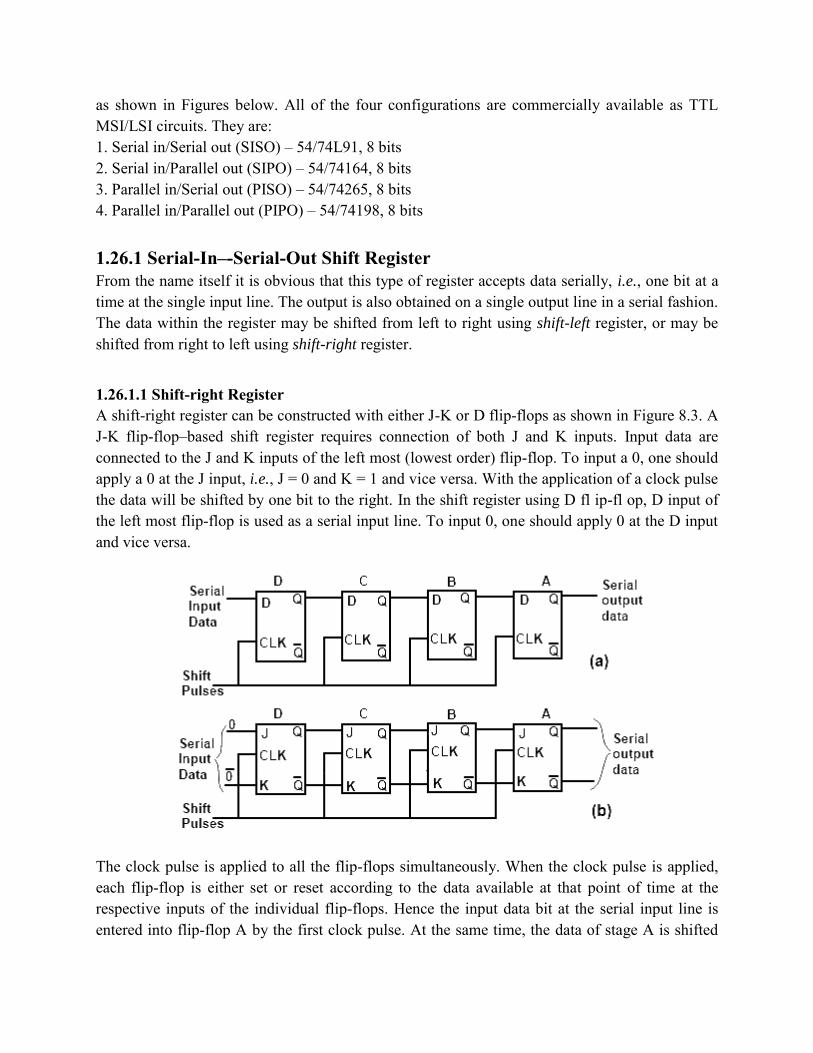
as shown in Figures below. All of the four configurations are commercially available as TTL MSI/LSI circuits. They are: 1. Serial in/Serial out (SISO) – 54/74L91, 8 bits 2. Serial in/Parallel out (SIPO) – 54/74164, 8 bits 3. Parallel in/Serial out (PISO) – 54/74265, 8 bits 4. Parallel in/Parallel out (PIPO) – 54/74198, 8 bits 1.26.1 Serial-In–-Serial-Out Shift Register From the name itself it is obvious that this type of register accepts data serially, i.e., one bit at a time at the single input line. The output is also obtained on a single output line in a serial fashion. The data within the register may be shifted from left to right using shift-left register, or may be shifted from right to left using shift-right register.
1.26.1.1 Shift-right Register A shift-right register can be constructed with either J-K or D flip-flops as shown in Figure 8.3. A J-K flip-flop–based shift register requires connection of both J and K inputs. Input data are connected to the J and K inputs of the left most (lowest order) flip-flop. To input a 0, one should apply a 0 at the J input, i.e., J = 0 and K = 1 and vice versa. With the application of a clock pulse the data will be shifted by one bit to the right. In the shift register using D fl ip-fl op, D input of the left most flip-flop is used as a serial input line. To input 0, one should apply 0 at the D input and vice versa.
The clock pulse is applied to all the flip-flops simultaneously. When the clock pulse is applied, each flip-flop is either set or reset according to the data available at that point of time at the respective inputs of the individual flip-flops. Hence the input data bit at the serial input line is entered into flip-flop A by the first clock pulse. At the same time, the data of stage A is shifted
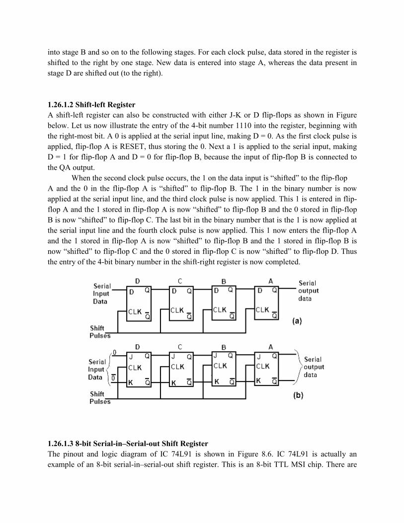
into stage B and so on to the following stages. For each clock pulse, data stored in the register is shifted to the right by one stage. New data is entered into stage A, whereas the data present in stage D are shifted out (to the right). 1.26.1.2 Shift-left Register A shift-left register can also be constructed with either J-K or D flip-flops as shown in Figure below. Let us now illustrate the entry of the 4-bit number 1110 into the register, beginning with the right-most bit. A 0 is applied at the serial input line, making D = 0. As the first clock pulse is applied, flip-flop A is RESET, thus storing the 0. Next a 1 is applied to the serial input, making D = 1 for flip-flop A and D = 0 for flip-flop B, because the input of flip-flop B is connected to the QA output.
When the second clock pulse occurs, the 1 on the data input is ―shifted‖ to the flip-flop A and the 0 in the flip-flop A is ―shifted‖ to flip-flop B. The 1 in the binary number is now applied at the serial input line, and the third clock pulse is now applied. This 1 is entered in flip-flop A and the 1 stored in flip-flop A is now ―shifted‖ to flip-flop B and the 0 stored in flip-flop B is now ―shifted‖ to flip-flop C. The last bit in the binary number that is the 1 is now applied at the serial input line and the fourth clock pulse is now applied. This 1 now enters the flip-flop A and the 1 stored in flip-flop A is now ―shifted‖ to flip-flop B and the 1 stored in flip-flop B is now ―shifted‖ to flip-flop C and the 0 stored in flip-flop C is now ―shifted‖ to flip-flop D. Thus the entry of the 4-bit binary number in the shift-right register is now completed.
1.26.1.3 8-bit Serial-in–Serial-out Shift Register The pinout and logic diagram of IC 74L91 is shown in Figure 8.6. IC 74L91 is actually an example of an 8-bit serial-in–serial-out shift register. This is an 8-bit TTL MSI chip. There are
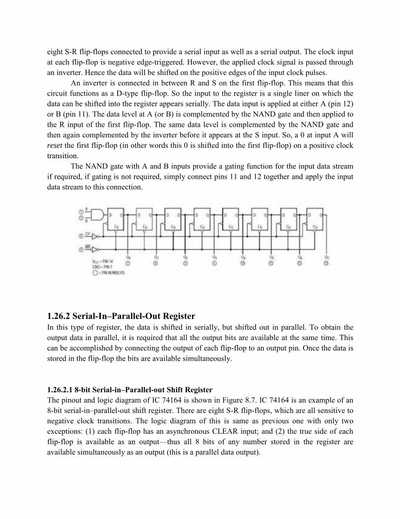
eight S-R flip-flops connected to provide a serial input as well as a serial output. The clock input at each flip-flop is negative edge-triggered. However, the applied clock signal is passed through an inverter. Hence the data will be shifted on the positive edges of the input clock pulses.
An inverter is connected in between R and S on the first flip-flop. This means that this circuit functions as a D-type flip-flop. So the input to the register is a single liner on which the data can be shifted into the register appears serially. The data input is applied at either A (pin 12) or B (pin 11). The data level at A (or B) is complemented by the NAND gate and then applied to the R input of the first flip-flop. The same data level is complemented by the NAND gate and then again complemented by the inverter before it appears at the S input. So, a 0 at input A will reset the first flip-flop (in other words this 0 is shifted into the first flip-flop) on a positive clock transition.
The NAND gate with A and B inputs provide a gating function for the input data stream if required, if gating is not required, simply connect pins 11 and 12 together and apply the input data stream to this connection.
1.26.2 Serial-In–Parallel-Out Register In this type of register, the data is shifted in serially, but shifted out in parallel. To obtain the output data in parallel, it is required that all the output bits are available at the same time. This can be accomplished by connecting the output of each flip-flop to an output pin. Once the data is stored in the flip-flop the bits are available simultaneously. 1.26.2.1 8-bit Serial-in–Parallel-out Shift Register The pinout and logic diagram of IC 74164 is shown in Figure 8.7. IC 74164 is an example of an 8-bit serial-in–parallel-out shift register. There are eight S-R flip-flops, which are all sensitive to negative clock transitions. The logic diagram of this is same as previous one with only two exceptions: (1) each flip-flop has an asynchronous CLEAR input; and (2) the true side of each flip-flop is available as an output—thus all 8 bits of any number stored in the register are available simultaneously as an output (this is a parallel data output).
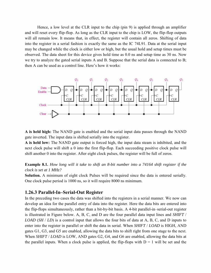
Hence, a low level at the CLR input to the chip (pin 9) is applied through an amplifier and will reset every flip-flop. As long as the CLR input to the chip is LOW, the flip-flop outputs will all remain low. It means that, in effect, the register will contain all zeros. Shifting of data into the register in a serial fashion is exactly the same as the IC 74L91. Data at the serial input may be changed while the clock is either low or high, but the usual hold and setup times must be observed. The data sheet for this device gives hold time as 0.0 ns and setup time as 30 ns. Now we try to analyze the gated serial inputs A and B. Suppose that the serial data is connected to B; then A can be used as a control line. Here‘s how it works:
A is held high: The NAND gate is enabled and the serial input data passes through the NAND gate inverted. The input data is shifted serially into the register. A is held low: The NAND gate output is forced high, the input data steam is inhibited, and the next clock pulse will shift a 0 into the first flip-flop. Each succeeding positive clock pulse will shift another 0 into the register. After eight clock pulses, the register will be full of zeros. Example 8.1. How long will it take to shift an 8-bit number into a 74164 shift register if the
clock is set at 1 MHz?
Solution. A minimum of eight clock Pulses will be required since the data is entered serially. One clock pulse period is 1000 ns, so it will require 8000 ns minimum. 1.26.3 Parallel-In–Serial-Out Register In the preceding two cases the data was shifted into the registers in a serial manner. We now can develop an idea for the parallel entry of data into the register. Here the data bits are entered into the flip-flops simultaneously, rather than a bit-by-bit basis. A 4-bit parallel-in–serial-out register is illustrated in Figure below. A, B, C, and D are the four parallel data input lines and SHIFT / LOAD (SH / LD) is a control input that allows the four bits of data at A, B, C, and D inputs to enter into the register in parallel or shift the data in serial. When SHIFT / LOAD is HIGH, AND gates G1, G3, and G5 are enabled, allowing the data bits to shift right from one stage to the next. When SHIFT / LOAD is LOW, AND gates G2, G4, and G6 are enabled, allowing the data bits at the parallel inputs. When a clock pulse is applied, the flip-flops with D = 1 will be set and the
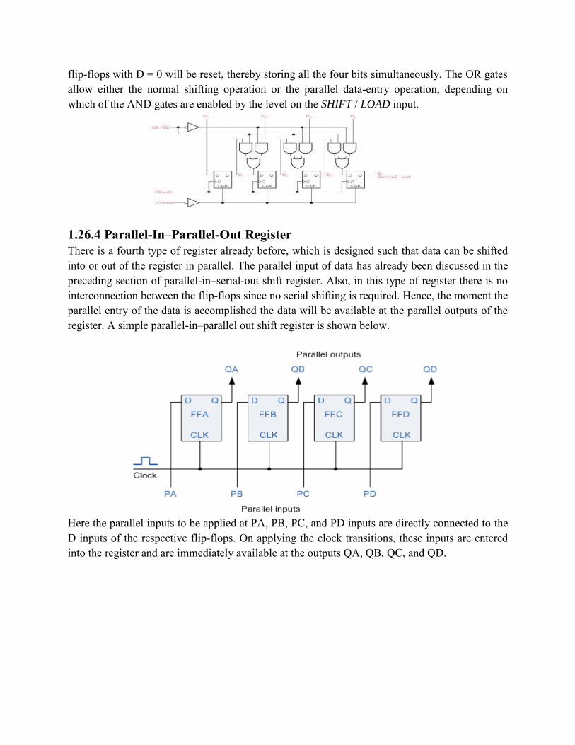
flip-flops with D = 0 will be reset, thereby storing all the four bits simultaneously. The OR gates allow either the normal shifting operation or the parallel data-entry operation, depending on which of the AND gates are enabled by the level on the SHIFT / LOAD input.
1.26.4 Parallel-In–Parallel-Out Register There is a fourth type of register already before, which is designed such that data can be shifted into or out of the register in parallel. The parallel input of data has already been discussed in the preceding section of parallel-in–serial-out shift register. Also, in this type of register there is no interconnection between the flip-flops since no serial shifting is required. Hence, the moment the parallel entry of the data is accomplished the data will be available at the parallel outputs of the register. A simple parallel-in–parallel out shift register is shown below.
Here the parallel inputs to be applied at PA, PB, PC, and PD inputs are directly connected to the D inputs of the respective flip-flops. On applying the clock transitions, these inputs are entered into the register and are immediately available at the outputs QA, QB, QC, and QD.
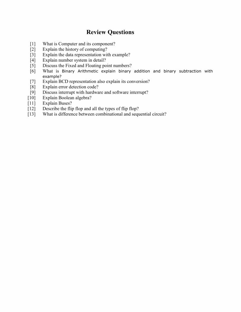
Review Questions
[1] What is Computer and its component? [2] Explain the history of computing? [3] Explain the data representation with example? [4] Explain number system in detail? [5] Discuss the Fixed and Floating point numbers? [6] What is Binary Arithmetic explain binary addition and binary subtraction with
example? [7] Explain BCD representation also explain its conversion? [8] Explain error detection code? [9] Discuss interrupt with hardware and software interrupt?
[10] Explain Boolean algebra? [11] Explain Buses? [12] Describe the flip flop and all the types of flip flop? [13] What is difference between combinational and sequential circuit?
2.1.Memory System
Memory is an essential part of any computer. These are used extensively for storing various types of program segments, data and other information. Essentially, they are expected to be read-write type of memory. Although, as described before, that a small amount of read-only memory (ROM) is essential for any computer system (boot strap ROM) at the time of power-on, we are not considering that aspect in our present discussions.
Memory Technologies
° Random Access:
• ―Random‖ is good: access time is the same for all locations
• DRAM: Dynamic Random Access Memory
- High density, low power, cheap, slow
- Dynamic: content must be ―refreshed‖ regularly
• SRAM: Static Random Access Memory
- Low density, high power, expensive, fast
- Static: content will last ―forever‖ (until lose power)
° ―Not-so-random‖ Access Technology:
• Access time varies from location to location and from time to time
• Examples: Disk, CDROM
° Sequential Access Technology: access time linear in location
(e.g.,Tape)
2.2.Memory Hierarchy
The term memory hierarchy is used in computer architecture when discussing performance issues in computer architectural design, algorithm predictions, and the lower level programming constructs such as involving locality of reference. A "memory hierarchy" incomputer storage distinguishes each level in the "hierarchy" by response time. Since response time, complexity, and capacity are related, the levels may also be distinguished by the controlling technology.
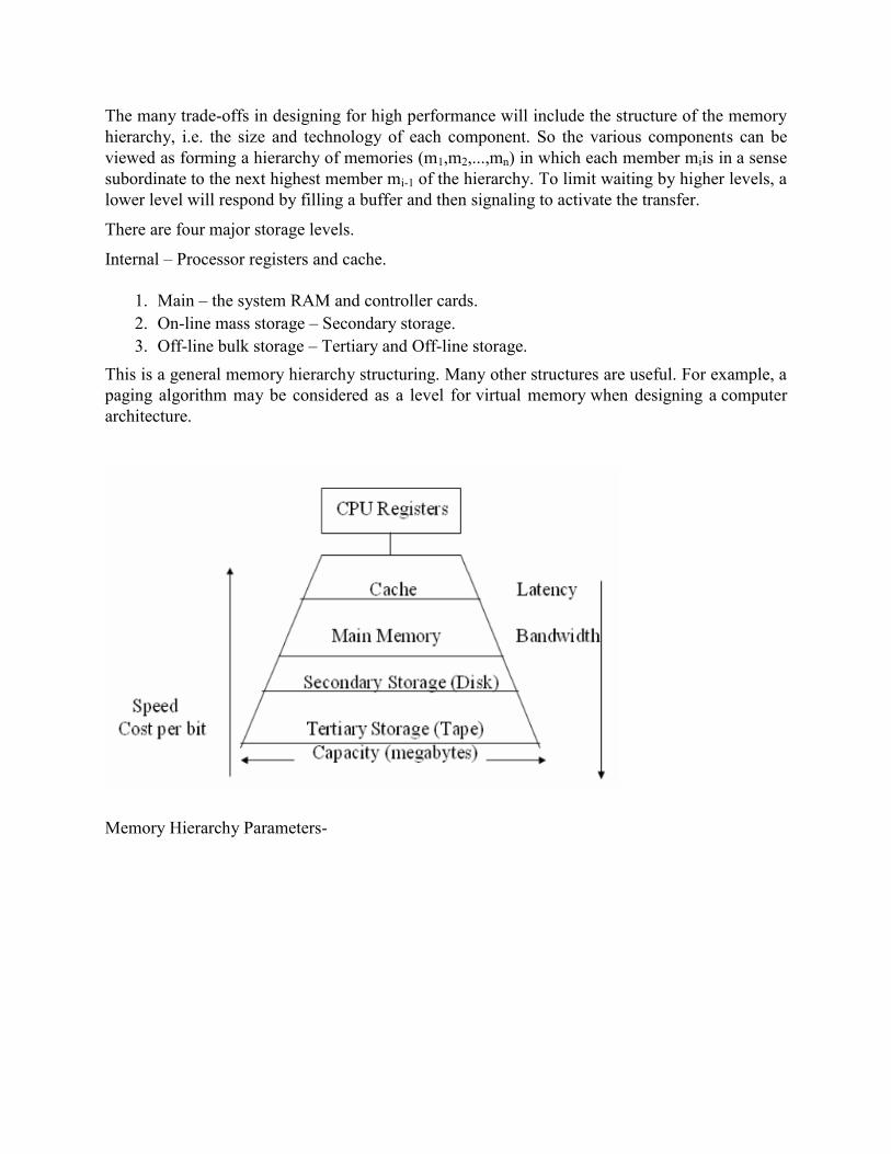
The many trade-offs in designing for high performance will include the structure of the memory hierarchy, i.e. the size and technology of each component. So the various components can be viewed as forming a hierarchy of memories (m1,m2,...,mn) in which each member miis in a sense subordinate to the next highest member mi-1 of the hierarchy. To limit waiting by higher levels, a lower level will respond by filling a buffer and then signaling to activate the transfer.
There are four major storage levels.
Internal – Processor registers and cache.
1. Main – the system RAM and controller cards. 2. On-line mass storage – Secondary storage. 3. Off-line bulk storage – Tertiary and Off-line storage.
This is a general memory hierarchy structuring. Many other structures are useful. For example, a paging algorithm may be considered as a level for virtual memory when designing a computer architecture.
Memory Hierarchy Parameters-
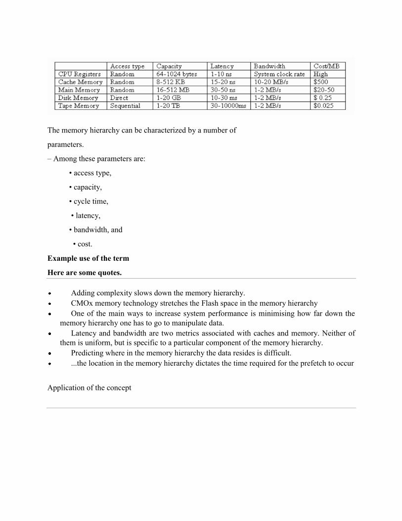
The memory hierarchy can be characterized by a number of
parameters.
– Among these parameters are:
• access type,
• capacity,
• cycle time,
• latency,
• bandwidth, and
• cost.
Example use of the term
Here are some quotes.
Adding complexity slows down the memory hierarchy. CMOx memory technology stretches the Flash space in the memory hierarchy One of the main ways to increase system performance is minimising how far down the
memory hierarchy one has to go to manipulate data. Latency and bandwidth are two metrics associated with caches and memory. Neither of
them is uniform, but is specific to a particular component of the memory hierarchy. Predicting where in the memory hierarchy the data resides is difficult. ...the location in the memory hierarchy dictates the time required for the prefetch to occur
Application of the concept
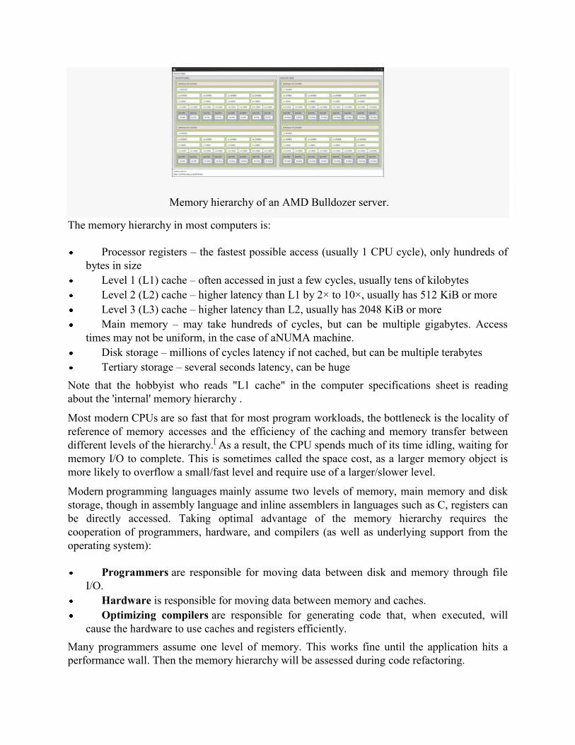
Memory hierarchy of an AMD Bulldozer server.
The memory hierarchy in most computers is:
Processor registers – the fastest possible access (usually 1 CPU cycle), only hundreds of bytes in size
Level 1 (L1) cache – often accessed in just a few cycles, usually tens of kilobytes Level 2 (L2) cache – higher latency than L1 by 2× to 10×, usually has 512 KiB or more Level 3 (L3) cache – higher latency than L2, usually has 2048 KiB or more Main memory – may take hundreds of cycles, but can be multiple gigabytes. Access
times may not be uniform, in the case of aNUMA machine. Disk storage – millions of cycles latency if not cached, but can be multiple terabytes Tertiary storage – several seconds latency, can be huge
Note that the hobbyist who reads "L1 cache" in the computer specifications sheet is reading about the 'internal' memory hierarchy .
Most modern CPUs are so fast that for most program workloads, the bottleneck is the locality of reference of memory accesses and the efficiency of the caching and memory transfer between different levels of the hierarchy.[ As a result, the CPU spends much of its time idling, waiting for memory I/O to complete. This is sometimes called the space cost, as a larger memory object is more likely to overflow a small/fast level and require use of a larger/slower level.
Modern programming languages mainly assume two levels of memory, main memory and disk storage, though in assembly language and inline assemblers in languages such as C, registers can be directly accessed. Taking optimal advantage of the memory hierarchy requires the cooperation of programmers, hardware, and compilers (as well as underlying support from the operating system):
Programmers are responsible for moving data between disk and memory through file I/O.
Hardware is responsible for moving data between memory and caches. Optimizing compilers are responsible for generating code that, when executed, will
cause the hardware to use caches and registers efficiently. Many programmers assume one level of memory. This works fine until the application hits a performance wall. Then the memory hierarchy will be assessed during code refactoring.
2.3.RAM
Random-access memory (RAM /ræm/) is a form of computer data storage. A random-access device allows stored data to be accessed directly in any random order. In contrast, other data storage media such as hard disks, CDs, DVDs and magnetic tape, as well as early primary memory types such as drum memory, read and write data only in a predetermined order, consecutively, because of mechanical design limitations. Therefore the time to access a given data location varies significantly depending on its physical location.
Today, random-access memory takes the form of integrated circuits. Strictly speaking, modern types of DRAM are not random access, as data is read in bursts, although the name DRAM / RAM has stuck. However, many types of SRAM, ROM, OTP, and NOR flash are still random access even in a strict sense. RAM is normally associated with volatile types of memory (such as DRAM memory modules), where its stored information is lost if the power is removed. Many other types of non-volatile memory are RAM as well, including most types of ROM and a type of flash memory called NOR-Flash. The first RAM modules to come into the market were created in 1951 and were sold until the late 1960s and early 1970s.
Types of RAM There are two different types of RAM:
DRAM (Dynamic Random Access Memory) SRAM (Static Random Access Memory).
2.4.DRAM-
DRAM stores a bit of data using a transistor and capacitor pair, which together comprise a memory cell. The capacitor holds a high or low charge (1 or 0, respectively), and the transistor acts as a switch that lets the control circuitry on the chip read the capacitor's state of charge or change it. As this form of memory is less expensive to produce than static RAM, it is the predominant form of computer memory used in modern computers.
2.5.SRAM-
In SRAM, a bit of data is stored using the state of a flip-flop. This form of RAM is more expensive to produce, but is generally faster and requires less power than DRAM and, in modern computers, is often used as cache memory for the CPU
Both static and dynamic RAM are considered volatile, as their state is lost or reset when power is removed from the system. By contrast, read-only memory (ROM) stores data by permanently enabling or disabling selected transistors, such that the memory cannot be altered. Writeable variants of ROM (such as EEPROM and flash memory) share properties of both ROM and
RAM, enabling data to persist without power and to be updated without requiring special equipment. These persistent forms of semiconductor ROM include USB flash drives, memory cards for cameras and portable devices, etc. ECC memory (which can be either SRAM or DRAM) includes special circuitry to detect and/or correct random faults (memory errors) in the stored data, using parity bitsor error correction code.
In general, the term RAM refers solely to solid-state memory devices (either DRAM or SRAM), and more specifically the main memory in most computers. In optical storage, the term DVD-RAMis somewhat of a misnomer since, unlike CD-RW or DVD-RW it does not need to be erased before reuse. Nevertheless a DVD-RAM behaves much like a hard disc drive if somewhat slower.
2.6.ROM
Read-only memory (ROM) is a class of storage medium used in computers and other electronic devices. Data stored in ROM cannot be modified, or can be modified only slowly or with difficulty, so it is mainly used to distribute firmware (software that is very closely tied to specific hardware, and unlikely to need frequent updates).
In its strictest sense, ROM refers only to mask ROM (the oldest type of solid state ROM), which is fabricated with the desired data permanently stored in it, and thus can never be modified. Despite the simplicity, speed and economies of scale of mask ROM, field-programmability often make reprogrammable memories more flexible and inexpensive. As of 2007, actual ROM circuitry is therefore mainly used for applications such as microcode, and similar structures, on various kinds of processors.
Other types of non-volatile memory such as erasable programmable read only memory (EPROM) and electrically erasable programmable read-only memory (EEPROM or Flash ROM) are sometimes referred to, in an abbreviated way, as "read-only memory" (ROM); although these types of memory can be erased and re-programmed multiple times, writing to this memory takes longer and may require different procedures than reading the memory.[1]When used in this less precise way, "ROM" indicates a non-volatile memory which serves functions typically provided by mask ROM, such as storage of program code and nonvolatile data.
Types-
Classic mask-programmed ROM chips are integrated circuits that physically encode the data to be stored, and thus it is impossible to change their contents after fabrication. Other types of non-volatile solid-state memory permit some degree of modification:
Programmable read-only memory (PROM), or one-time programmable ROM (OTP), can be written to or programmed via a special device called a PROM programmer. Typically, this device uses high voltages to permanently destroy or create internal links (fuses or antifuses) within the chip. Consequently, a PROM can only be programmed once.
Erasable programmable read-only memory (EPROM) can be erased by exposure to strong ultraviolet light (typically for 10 minutes or longer), then rewritten with a process that again needs higher than usual voltage applied. Repeated exposure to UV light will eventually wear out an EPROM, but the endurance of most EPROM chips exceeds 1000 cycles of erasing and reprogramming. EPROM chip packages can often be identified by the prominent quartz "window" which allows UV light to enter. After programming, the window is typically covered with a label to prevent accidental erasure. Some EPROM chips are factory-erased before they are packaged, and include no window; these are effectively PROM.
Electrically erasable programmable read-only memory (EEPROM) is based on a similar semiconductor structure to EPROM, but allows its entire contents (or selected banks) to be electrically erased, then rewritten electrically, so that they need not be removed from the computer (or camera, MP3 player, etc.). Writing or flashing an EEPROM is much slower (milliseconds per bit) than reading from a ROM or writing to a RAM (nanoseconds in both cases).
Electrically alterable read-only memory (EAROM) is a type of EEPROM that can be modified one bit at a time. Writing is a very slow process and again needs higher voltage (usually around 12 V) than is used for read access. EAROMs are intended for applications that require infrequent and only partial rewriting. EAROM may be used as non-volatile storage for critical system setup information; in many applications, EAROM has been supplanted by CMOS RAM supplied by mains power and backed-up with a lithium battery.
2.7.Flash memeory
Flash memory (or simply flash) is a modern type of EEPROM invented in 1984. Flash memory can be erased and rewritten faster than ordinary EEPROM, and newer designs feature very high endurance (exceeding 1,000,000 cycles). Modern NAND flash makes efficient use of silicon chip area, resulting in individual ICs with a capacity as high as 32 GB as of 2007; this feature, along with its endurance and physical durability, has allowed NAND flash to replace magnetic in some applications (such as USB flash drives). Flash memory is sometimes calledflash ROM or flash EEPROM when used as a replacement for older ROM types, but not in applications that take advantage of its ability to be modified quickly and frequently.
2.8.Need of secondary storage technologies As of 2011, the most commonly used data storage technologies are semiconductor, magnetic, and optical, while paper still sees some limited usage. Media is a common name for what actually holds the data in the storage device. Some other fundamental storage technologies have also been used in the past or are proposed for development.
Semiconductor Semiconductor memory uses semiconductor-based integrated circuits to store information. A semiconductor memory chip may contain millions of tiny transistors or capacitors. Both volatile andnon-volatile forms of semiconductor memory exist. In modern computers, primary storage almost exclusively consists of dynamic volatile semiconductor memory or dynamic random access memory. Since the turn of the century, a type of non-volatile semiconductor memory known as flash memory has steadily gained share as off-line storage for home computers. Non-volatile semiconductor memory is also used for secondary storage in various advanced electronic devices and specialized computers. As early as 2006, notebook and desktop computer manufacturers started using flash-based solid-state drives (SSDs) as default configuration options for the secondary storage either in addition to or instead of the more traditional HDD Magnetic Magnetic storage uses different patterns of magnetization on a magnetically coated surface to store information. Magnetic storage is non-volatile. The information is accessed using one or more read/write heads which may contain one or more recording transducers. A read/write head only covers a part of the surface so that the head or medium or both must be moved relative to another in order to access data. In modern computers, magnetic storage will take these forms:
Magnetic disk Floppy disk, used for off-line storage Hard disk drive, used for secondary storage
Magnetic tape, used for tertiary and off-line storage In early computers, magnetic storage was also used as:
Primary storage in a form of magnetic memory, or core memory, core rope memory, thin-film memory and/or twistor memory.
Tertiary (e.g. NCR CRAM) or off line storage in the form of magnetic cards. Magnetic tape was then often used for secondary storage.
Optical Optical storage, the typical optical disc, stores information in deformities on the surface of a circular disc and reads this information by illuminating the surface with a laser diode and observing the reflection. Optical disc storage is non-volatile. The deformities may be permanent (read only media ), formed once (write once media) or reversible (recordable or read/write media). The following forms are currently in common use CD, CD-ROM, DVD, BD-ROM: Read only storage, used for mass distribution of digital information (music, video, computer programs)
CD-R, DVD-R, DVD+R, BD-R: Write once storage, used for tertiary and off-line storage CD-RW, DVD-RW, DVD+RW, DVD-RAM, BD-RE: Slow write, fast read storage, used
for tertiary and off-line storage
Ultra Density Optical or UDO is similar in capacity to BD-R or BD-RE and is slow write, fast read storage used for tertiary and off-line storage.
Magneto-optical disc storage is optical disc storage where the magnetic state on a ferromagnetic surface stores information. The information is read optically and written by combining magnetic and optical methods. Magneto-optical disc storage is non-volatile, sequential access, slow write, fast read storage used for tertiary and off-line storage.
3D optical data storage has also been proposed.
Paper Paper data storage, typically in the form of paper tape or punched cards, has long been used to store information for automatic processing, particularly before general-purpose computers existed. Information was recorded by punching holes into the paper or cardboard medium and was read mechanically (or later optically) to determine whether a particular location on the medium was solid or contained a hole. A few technologies allow people to make marks on paper that are easily read by machine—these are widely used for tabulating votes and grading standardized tests.Barcodes made it possible for any object that was to be sold or transported to have some computer readable information securely attached to it. Uncommon Vacuum tube memory
A Williams tube used a cathode ray tube, and a Selectron tube used a large vacuum tube to store information. These primary storage devices were short-lived in the market, since Williams tube was unreliable and the Selectron tube was expensive.
Electro-acoustic memory Delay line memory used sound waves in a substance such as mercury to store information. Delay line memory was dynamic volatile, cycle sequential read/write storage, and was used for primary storage.
Optical tape is a medium for optical storage generally consisting of a long and narrow strip of plastic onto which patterns can be written and from which the patterns can be read back. It shares some technologies with cinema film stock and optical discs, but is compatible with neither. The motivation behind developing this technology was the possibility of far greater storage capacities than either magnetic tape or optical discs.
Phase-change memory uses different mechanical phases of Phase Change Material to store information in an X-Y addressable matrix, and reads the information by observing the varying electrical resistance of the material. Phase-change memory would be non-volatile, random-access read/write storage, and might be used for primary, secondary and off-line storage. Most
rewritable and many write once optical disks already use phase change material to store information.
Holographic data storage stores information optically inside crystals or photopolymers. Holographic storage can utilize the whole volume of the storage medium, unlike optical disc storage which is limited to a small number of surface layers. Holographic storage would be non-volatile, sequential access, and either write once or read/write storage. It might be used for secondary and off-line storage. SeeHolographic Versatile Disc (HVD).
Molecular memory stores information in polymer that can store electric charge. Molecular memory might be especially suited for primary storage. The theoretical storage capacity of molecular memory is 10 terabits per square inch.
Related technologies
Disk storage replication
While a group of bits malfunction may be resolved by error detection and correction mechanisms (see above), storage device malfunction requires different solutions. The following solutions are commonly used and valid for most storage devices:
1.Device mirroring (replication) - A common solution to the problem is constantly maintaining an identical copy of device content on another device (typically of a same type). The downside is that this doubles the storage, and both devices (copies) need to be updated simultaneously with some overhead and possibly some delays. The upside is possible concurrent read of a same data group by two independent processes, which increases performance. When one of the replicated devices is detected to be defective, the other copy is still operational, and is being utilized to generate a new copy on another device (usually available operational in a pool of stand-by devices for this purpose).
2.Redundant array of independent disks (RAID) - This method generalizes the device mirroring above by allowing one device in a group of N devices to fail and be replaced with content restored (Device mirroring is RAID with N=2). RAID groups of N=5 or N=6 are common. N>2 saves storage, when comparing with N=2, at the cost of more processing during both regular operation (with often reduced performance) and defective device replacement. Device mirroring and typical RAID are designed to handle a single device failure in the RAID group of devices. However, if a second failure occurs before the RAID group is completely repaired from the first failure, then data can be lost. The probability of a single failure is typically small. Thus the probability of two failures in a same RAID group in time proximity is much
smaller (approximately the probability squared, i.e., multiplied by itself). If a database cannot tolerate even such smaller probability of data loss, then the RAID group itself is replicated (mirrored). In many cases such mirroring is done geographically remotely, in a different storage array, to handle also recovery from disasters (see disaster recovery above).
Network connectivity A secondary or tertiary storage may connect to a computer utilizing computer networks. This concept does not pertain to the primary storage, which is shared between multiple processors to a lesser degree.
1.Direct-attached storage (DAS) is a traditional mass storage, that does not use any network. This is still a most popular approach. This retronym was coined recently, together with NAS and SAN.
2.Network-attached storage (NAS) is mass storage attached to a computer which another computer can access at file level over a local area network, a private wide area network, or in the case of online file storage, over the Internet. NAS is commonly associated with the NFS and CIFS/SMB protocols.
3.Storage area network (SAN) is a specialized network, that provides other computers with storage capacity. The crucial difference between NAS and SAN is the former presents and manages file systems to client computers, whilst the latter provides access at block-addressing (raw) level, leaving it to attaching systems to manage data or file systems within the provided capacity. SAN is commonly associated with Fibre Channel networks. Robotic storage Large quantities of individual magnetic tapes, and optical or magneto-optical discs may be stored in robotic tertiary storage devices. In tape storage field they are known as tape libraries, and in optical storage field optical jukeboxes, or optical disk libraries per analogy. Smallest forms of either technology containing just one drive device are referred to as autoloaders or autochangers. Robotic-access storage devices may have a number of slots, each holding individual media, and usually one or more picking robots that traverse the slots and load media to built-in drives. The arrangement of the slots and picking devices affects performance. Important characteristics of such storage are possible expansion options: adding slots, modules, drives, robots. Tape libraries may have from 10 to more than 100,000 slots, and provide terabytes or petabytes of near-line information. Optical jukeboxes are somewhat smaller solutions, up to 1,000 slots.
Robotic storage is used for backups, and for high-capacity archives in imaging, medical, and video industries. Hierarchical storage management is a most known archiving strategy of automatically migrating long-unused files from fast hard disk storage to libraries or jukeboxes. If the files are needed, they are retrieved back to disk.
2.9.Secondary memory
Secondary storage (also known as external memory or auxiliary storage), differs from primary storage in that it is not directly accessible by the CPU. The computer usually uses its input/output channels to access secondary storage and transfers the desired data using intermediate area in primary storage. Secondary storage does not lose the data when the device is powered down—it is non-volatile. Per unit, it is typically also two orders of magnitude less expensive than primary storage. Modern computer systems typically have two orders of magnitude more secondary storage than primary storage and data are kept for a longer time there.
In modern computers, hard disk drives are usually used as secondary storage. The time taken to access a given byte of information stored on a hard disk is typically a few thousandths of a second, or milliseconds. By contrast, the time taken to access a given byte of information stored in random-access memory is measured in billionths of a second, or nanoseconds. This illustrates the significant access-time difference which distinguishes solid-state memory from rotating magnetic storage devices: hard disks are typically about a million times slower than memory. Rotating optical storagedevices, such as CD and DVD drives, have even longer access times. With disk drives, once the disk read/write head reaches the proper placement and the data of interest rotates under it, subsequent data on the track are very fast to access. To reduce the seek time and rotational latency, data are transferred to and from disks in large contiguous blocks.
When data reside on disk, block access to hide latency offers a ray of hope in designing efficient external memory algorithms. Sequential or block access on disks is orders of magnitude faster than random access, and many sophisticated paradigms have been developed to design efficient algorithms based upon sequential and block access. Another way to reduce the I/O bottleneck is to use multiple disks in parallel in order to increase the bandwidth between primary and secondary memory.[3]
Some other examples of secondary storage technologies are: flash memory (e.g. USB flash drives or keys), floppy disks, magnetic tape, paper tape, punched cards, standalone RAM disks, andIomega Zip drives.
The secondary storage is often formatted according to a file system format, which provides the abstraction necessary to organize data into files and directories, providing also additional information (called metadata) describing the owner of a certain file, the access time, the access permissions, and other information.
Most computer operating systems use the concept of virtual memory, allowing utilization of more primary storage capacity than is physically available in the system. As the primary memory fills up, the system moves the least-used chunks (pages) to secondary storage devices (to a swap file or page file), retrieving them later when they are needed. As more of these retrievals from slower secondary storage are necessary, the more the overall system performance is degraded.
2.9.1.Characteristics Storage technologies at all levels of the storage hierarchy can be differentiated by evaluating certain core characteristics as well as measuring characteristics specific to a particular implementation. These core characteristics are volatility, mutability, accessibility, and addressibility. For any particular implementation of any storage technology, the characteristics worth measuring are capacity and performance.
Volatility Non-volatile memory
Will retain the stored information even if it is not constantly supplied with electric power. It is suitable for long-term storage of information.
Volatile memory
Requires constant power to maintain the stored information. The fastest memory technologies of today are volatile ones (not a universal rule). Since primary storage is required to be very fast, it predominantly uses volatile memory.
Dynamic random-access memory A form of volatile memory which also requires the stored information to be periodically re-read and re-written, or refreshed, otherwise it would vanish. Static random-access memory A form of volatile memory similar to DRAM with the exception that it never needs to be refreshed as long as power is applied. (It loses its content if power is removed). An uninterruptible power supply can be used to give a computer a brief window of time to move information from primary volatile storage into non-volatile storage before the batteries are exhausted. Some systems (e.g., see the EMC Symmetrix) have integrated batteries that maintain volatile storage for several hours.
Mutability Read/write storage or mutable storage
Allows information to be overwritten at any time. A computer without some amount of read/write storage for primary storage purposes would be useless for many tasks. Modern computers typically use read/write storage also for secondary storage. Read only storage Retains the information stored at the time of manufacture, and write once storage (Write Once Read Many) allows the information to be written only once at some point after manufacture. These are called immutable storage. Immutable storage is used for tertiary and off-line storage. Examples include CD-ROM and CD-R. Slow write, fast read storage
Read/write storage which allows information to be overwritten multiple times, but with the write operation being much slower than the read operation. Examples include CD-RW and flash memory. Accessibility Random access Any location in storage can be accessed at any moment in approximately the same amount of time. Such characteristic is well suited for primary and secondary storage. Most semiconductor memories and disk drives provide random access.
Sequential access The accessing of pieces of information will be in a serial order, one after the other; therefore the time to access a particular piece of information depends upon which piece of information was last accessed. Such characteristic is typical of off-line storage. Addressability Location-addressable
Each individually accessible unit of information in storage is selected with its numerical memory address. In modern computers, location-addressable storage usually limits to primary storage, accessed internally by computer programs, since location-addressability is very efficient, but burdensome for humans. File addressable Information is divided into files of variable length, and a particular file is selected with human-readable directory and file names. The underlying device is still location-addressable, but theoperating system of a computer provides the file system abstraction to make the operation more understandable. In modern computers, secondary, tertiary and off-line storage use file systems. Content-addressable Each individually accessible unit of information is selected based on the basis of (part of) the contents stored there. Content-addressable storage can be implemented using software(computer program) or hardware (computer device), with hardware being faster but more expensive option. Hardware content addressable memory is often used in a computer's CPU cache.
Capacity Raw capacity
The total amount of stored information that a storage device or medium can hold. It is expressed as a quantity of bits or bytes (e.g. 10.4 megabytes). Memory storage density The compactness of stored information. It is the storage capacity of a medium divided with a unit of length, area or volume (e.g. 1.2 megabytes per square inch). Performance Latency
The time it takes to access a particular location in storage. The relevant unit of measurement is typically nanosecond for primary storage, millisecond for secondary storage, and second for tertiary storage. It may make sense to separate read latency and write latency, and in case of sequential access storage, minimum, maximum and average latency. Throughput The rate at which information can be read from or written to the storage. In computer data storage, throughput is usually expressed in terms of megabytes per second or MB/s, though bit ratemay also be used. As with latency, read rate and write rate may need to be differentiated. Also accessing media sequentially, as opposed to randomly, typically yields maximum throughput. Granularity The size of the largest "chunk" of data that can be efficiently accessed as a single unit, e.g. without introducing more latency. Reliability The probability of spontaneous bit value change under various conditions, or overall failure rate Energy use Storage devices that reduce fan usage, automatically shut-down during inactivity, and low power hard drives can reduce energy consumption 90 percent.
2.5 inch hard disk drives often consume less power than larger ones.Low capacity solid-state drives have no moving parts and consume less power than hard disks.Also, memory may use more power than hard disks.
2.10.Optical Memories
Optical storage devices use light to store and retrieve data
• Devices that use this technology include CD-ROM, CD-Rs, CD-RWs and DVDs
• The CD-ROM is read using a low-power laser beam coming from the computer drive
• Low-power laser beam passes in front of the simulated pits and lands.
• For a land, the beam reaches the reflective layer and is reflected.
• For a simulated pit, the spot is opaque and not reflected.
Compact Disk• First made in 1983.• Compact Disk types• CR-Read only• CD-Recordable• CD-R/W• Data is encoded and read optically with a laser• Can store around 600MB to 700MB data
Data representation in CD-ROM• Digital data is represented as a series of Pits andLands:– Pit = a little depression, forming a lower level in the track– Land = the flat part between pits, or the upper levels in thetrack
Organization of data• Reading a CD is done by shining a laser at the disc anddetecting changing reflections patterns.– 1 = change in height (land to pit or pit to land)– 0 = a ―fixed‖ amount of
time between 1‘sLAND PIT LAND PIT LAND...------+ +-------------+ +---...|_____| |_______|..0 0 0 0 1 0 0 1 0 0 0 0 0 0 1 0 0 0 1 0 0 ..• Note : we cannot have two 1‘s in a row!
CD-ROM• Because of the heritage from CD audio, the data is storedas a single spiral track on
the CD-ROM, contrary tomagnetic hard disk‘s discrete track concept.• Thus, the rotation speed
is controlled by CLV-ConstantLinear velocity. The rotational speed at the center ishighest, slowing down towards the outer edge. Because,the recording density is the same every where.•
Note that with CLV, the linear speed of the spiral passingunder the R/W head remains constant.•
CLV is the result for the poor seek time in CD-ROMs• The advantage of CLV is that the disk is
utilized at its bestcapacity, as the recording density is the same every where.
CD-ROM• Note that: Since 0s are represented by the length oftime between transitions, we must travel at constantlinear velocity (CLV)on the tracks.• Sectors are organized along a spiral•
Sectors have same linear length• Advantage: takes advantage of all storage spaceavailable.•
Disadvantage: has to change rotational speed whenseeking (slower towards the outside)
Digital Versatile Disc•The DVD (Digital Video Disc or Digital Versatile Disc)technology is
based on CD technology withincreased storage density.• The DVD‘s come with a storage
capacity of up to17GB• Multi-layer• Very high capacity (4.7GB to 17GB)• Has same three types
as CD
2.11.Hard disk drives
A hard disk drive (HDD) is a data storage device used for storing and retrieving digital information using rapidly rotating disks (platters) coated with magnetic material. An HDD retains its data even when powered off. Data is read in a random-access manner, meaning individual blocks of data can be stored or retrieved in any order rather than sequentially. An HDD consists of one or more rigid ("hard") rapidly rotating disks (platters) withmagnetic heads arranged on a moving actuator arm to read and write data to the surfaces.
Introduced by IBM in 1956 HDDs became the dominant secondary storage device for general purpose computers by the early 1960s. Continuously improved, HDDs have maintained this position into the modern era of servers and personal computers. More than 200 companies have produced HDD units, though most current units are manufactured by Seagate, Toshiba and Western Digital. Worldwide revenues for HDD shipments are expected to reach $33 billion in 2013, a decrease of approximately 12% from $37.8 billion in 2012.
The primary characteristics of an HDD are its capacity and performance. Capacity is specified in unit prefixes corresponding to powers of 1000: a 1-terabyte (TB) drive has a capacity of 1,000 gigabytes (GB; where 1 gigabyte = 1 billion bytes). Typically, some of an HDD's capacity is unavailable to the user because it is used by the file system and the computer operating system, and possibly inbuilt redundancy for error correction and recovery. Performance is specified by the time to move the heads to a file (Average Access Time) plus the time it takes for the file to move under its head (average latency, a function of the physical rotational speed in revolutions per minute) and the speed at which the file is transmitted (data rate).
The two most common form factors for modern HDDs are 3.5-inch in desktop computers and 2.5-inch in laptops. HDDs are connected to systems bystandard interface cables such as SATA (Serial ATA), USB or SAS (Serial attached SCSI) cables.
As of 2012, the primary competing technology for secondary storage is flash memory in the form of solid-state drives (SSDs). HDDs are expected to remain the dominant medium for secondary storage due to predicted continuing advantages in recording capacity and price per unit of storage but SSDs are replacing HDDs where speed, power consumption and durability are more important considerations than price and capacity.
2.12.Head Mechanisms
Disk storage is a general category of storage mechanisms where data are recorded by various electronic, magnetic, optical, or mechanical changes to a surface layer of one or more rotatingdisks. A disk drive is a device implementing such a storage mechanism and is usually distinguished from the disk medium. Notable types are the hard disk drive (HDD) containing a non-removable disk, the floppy disk drive (FDD) and its removable floppy disk, and various optical disc drives and associated optical disc media.
Disk and disc are used interchangeably except where trademarks preclude one usage, e.g. the Compact Disc logo. The choice of a particular form is frequently historical, as in IBM's usage of the disk form beginning in 1956 with the "IBM 350 disk storage unit".
Access methods
Digital disk drives are block storage devices. Each disk is divided into logical blocks (collection of sectors). Blocks are addressed using their logical block addresses (LBA). Read from or writing to disk happens at the granularity of blocks.
Originally the disk capacity was quite low and has been improved in one of several ways. Improvements in mechanical design and manufacture allowed smaller and more precise heads, meaning that more tracks could be stored on each of the disks. Advancements in data compression methods permitted more information to be stored in each of the individual sectors.
The drive stores data onto cylinders, heads, and sectors. The sectors unit is the smallest size of data to be stored in a hard disk drive and each file will have many sectors units assigned to it. The smallest entity in a CD is called a frame, which consists of 33 bytes and contains six complete 16-bit stereo samples (two bytes × two channels × six samples = 24 bytes). The other nine bytes consist of eight CIRC error-correction bytes and onesubcode byte used for control and display.
The information is sent from the computer processor to the BIOS into a chip controlling the data transfer. This is then sent out to the hard drive via a multi-wire connector. Once the data is received onto the circuit board of the drive, it is translated and compressed into a format that the individual drive can use to store onto the disk itself. The data is then passed to a chip on the circuit board that controls the access to the drive. The drive is divided into sectors of data stored onto one of the sides of one of the internal disks. An HDD with two disks internally will typically store data on all four surfaces.
The hardware on the drive tells the actuator arm where it is to go for the relevant track and the compressed information is then sent down to the head which changes the physical properties, optically or magnetically for example, of each byte on the drive, thus storing the information. A file is not stored in a linear manner, rather, it is held in the best way for quickest retrieval.
Rotation speed and track layout
Mechanically there are two different motions occurring inside the drive. One is the rotation of the disks inside the device. The other is the side-to-side motion of the heads across the disk as it moves between tracks.
There are two types of disk rotation methods:
constant linear velocity (used mainly in optical storage) varies the rotational speed of the optical disc depending upon the position of the head, and
constant angular velocity (used in HDDs, standard FDDs, a few optical disc systems, and vinyl audio records) spins the media at one constant speed regardless of where the head is positioned.
Track positioning also follows two different methods across disk storage devices. Storage devices focused on holding computer data, e.g., HDDs, FDDs, Iomega zip drives, use concentric tracks to store data. During a sequential read or write operation, after the drive accesses all the sectors in a track it repositions the head(s) to the next track. This will cause a momentary delay in the flow of data between the device and the computer. In contrast, optical audio and video discs use a single spiral track that starts at the inner most point on the disc and flows continuously to the outer edge. When reading or writing data there is no need to stop the flow of data to switch tracks. This is similar to vinyl records except vinyl records started at the outer edge and spiraled in toward the center.
Interfaces
The disk drive interface is the mechanism/protocol of communication between the rest of the system and the disk drive itself. Storage devices intended for desktop and mobile computers typically use ATA (PATA) and SATA interfaces. Enterprise systems and high-end storage devices will typically use SCSI, SAS, and FC interfaces in addition to some use of SATA.
Basic terminology
Platter – An individual recording disk. In a hard disk drive we tend to find a set of platters and developments in optical technology have led to multiple recording layers on a single DVD's.
Spindle – the spinning axle on which the platters are mounted. Rotation – Platters rotate; two techniques are common:
Constant angular velocity (CAV) keeps the disk spinning at a fixed rate, measured in revolutions per minute (RPM). This means the heads cover more distance per unit of time on the outer tracks than on the inner tracks. This method is typical with computer hard drives.
Constant linear velocity (CLV) keeps the distance covered by the heads per unit time fixed. Thus the disk has to slow down as the arm moves to the outer tracks. This method is typical for CD drives.
Track – The circle of recorded data on a single recording surface of a platter. Sector – A segment of a track Low level formatting – Establishing the tracks and sectors. Head – The device that reads and writes the information—magnetic or optical—on the
disk surface. Arm – The mechanical assembly that supports the head as it moves in and out. Seek time – Time needed to move the head to a new position (specific track). Rotational latency – Average time, once the arm is on the right track, before a head is
over a desired sector. Data transfer rate - The rate at which user data bits are transferred from or to the medium,
technically this would more accurately be entitled the "gross" data transfer rate.
2.13.CCDs Modern scanners typically use a charge-coupled device (CCD) or a Contact Image Sensor (CIS) as the image sensor, whereas older drum scanners use a photomultiplier tube as the image sensor. A rotary scanner, used for high-speed document scanning, is another type of drum scanner, using a CCD array instead of a photomultiplier. Other types of scanners are planetary scanners, which take photographs of books and documents, and 3D scanners, for producing three-dimensional models of objects.
Another category of scanner is digital camera scanners, which are based on the concept of reprographic cameras. Due to increasing resolution and new features such as anti-shake, digital cameras have become an attractive alternative to regular scanners. While still having disadvantages compared to traditional scanners (such as distortion, reflections, shadows, low contrast), digital cameras offer advantages such as speed, portability and gentledigitizing of thick documents without damaging the book spine. New scanning technologies are combining 3D scanners with digital cameras to create full-color, photo-realistic 3D models of objects.[citation
needed]
In the biomedical research area, detection devices for DNA microarrays are called scanners as well. These scanners are high-resolution systems (up to 1 µm/ pixel), similar to microscopes. The detection is done via CCD or a photomultiplier tube (PMT)
Types- Drum Drum scanners capture image information with photomultiplier tubes (PMT), rather than the charge-coupled device (CCD) arrays found in flatbed scanners and inexpensive film scanners. Reflective and transmissive originals are mounted on an acrylic cylinder, the scanner drum, which rotates at high speed while it passes the object being scanned in front of precision optics that deliver image information to the PMTs. Most modern color drum scanners use three matched PMTs, which read red, blue, and green light, respectively. Light from the original artwork is split into separate red, blue, and green beams in the optical bench of the scanner.
The drum scanner gets its name from the clear acrylic cylinder, the drum, on which the original artwork is mounted for scanning. Depending on size, it is possible to mount originals up to 20"x28", but maximum size varies by manufacturer. One of the unique features of drum scanners is the ability to control sample area and aperture size independently. The sample size is the area that the scanner encoder reads to create an individual pixel. The aperture is the actual opening that allows light into the optical bench of the scanner. The ability to control aperture and sample size separately is particularly useful for smoothing film grain when scanning black-and white and color negative originals.
While drum scanners are capable of scanning both reflective and transmissive artwork, a good-quality flatbed scanner can produce good scans from reflective artwork. As a result, drum scanners are rarely used to scan prints now that high-quality, inexpensive flatbed scanners are readily available. Film, however, is where drum scanners continue to be the tool of choice for high-end applications. Because film can be wet-mounted to the scanner drum and because of the
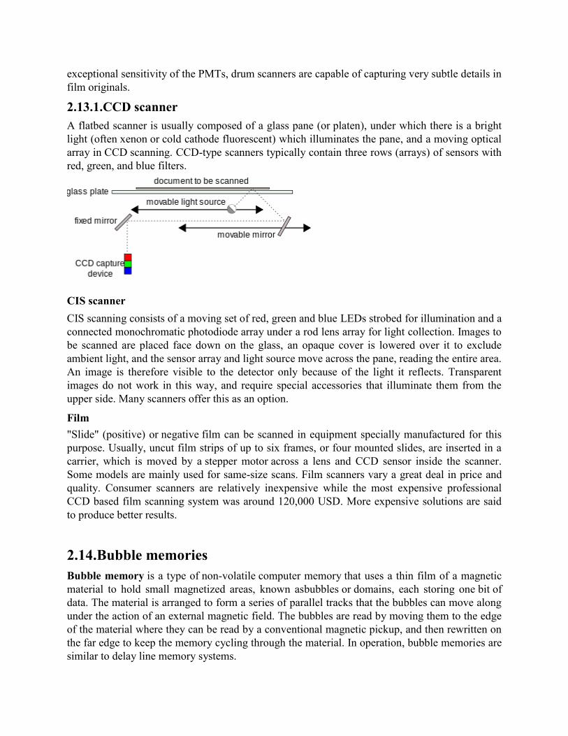
exceptional sensitivity of the PMTs, drum scanners are capable of capturing very subtle details in film originals.
2.13.1.CCD scanner A flatbed scanner is usually composed of a glass pane (or platen), under which there is a bright light (often xenon or cold cathode fluorescent) which illuminates the pane, and a moving optical array in CCD scanning. CCD-type scanners typically contain three rows (arrays) of sensors with red, green, and blue filters.
CIS scanner CIS scanning consists of a moving set of red, green and blue LEDs strobed for illumination and a connected monochromatic photodiode array under a rod lens array for light collection. Images to be scanned are placed face down on the glass, an opaque cover is lowered over it to exclude ambient light, and the sensor array and light source move across the pane, reading the entire area. An image is therefore visible to the detector only because of the light it reflects. Transparent images do not work in this way, and require special accessories that illuminate them from the upper side. Many scanners offer this as an option.
Film "Slide" (positive) or negative film can be scanned in equipment specially manufactured for this purpose. Usually, uncut film strips of up to six frames, or four mounted slides, are inserted in a carrier, which is moved by a stepper motor across a lens and CCD sensor inside the scanner. Some models are mainly used for same-size scans. Film scanners vary a great deal in price and quality. Consumer scanners are relatively inexpensive while the most expensive professional CCD based film scanning system was around 120,000 USD. More expensive solutions are said to produce better results.
2.14.Bubble memories Bubble memory is a type of non-volatile computer memory that uses a thin film of a magnetic material to hold small magnetized areas, known asbubbles or domains, each storing one bit of data. The material is arranged to form a series of parallel tracks that the bubbles can move along under the action of an external magnetic field. The bubbles are read by moving them to the edge of the material where they can be read by a conventional magnetic pickup, and then rewritten on the far edge to keep the memory cycling through the material. In operation, bubble memories are similar to delay line memory systems.
Bubble memory started out as a promising technology in the 1980s, offering memory density of a similar order as hard drives but performance more comparable to core memory. This led many to consider it a contender for a "universal memory" that could be used for all storage needs. However, the introduction of dramatically faster semiconductor memory chips pushed bubble into the slow end of the scale, and equally dramatic improvements in hard drive capacity made it uncompetitive in price terms.[1] Bubble memory was used for some time in the 1970s and 80s where its non-moving nature was desirable for maintenance or shock-proofing reasons. The introduction of Flash RAM and similar technologies rendered even this niche uncompetitive, and bubble disappeared entirely by the late 1980s.
Prehistory: twistor memory
Bubble memory is largely the brainchild of a single person, Andrew Bobeck. Bobeck had worked on many kinds of magnetics-related projects through the 1960s, and two of his projects put him in a particularly good position for the development of bubble memory. The first was the development of the first magnetic core memory system driven by a transistor-based controller, and the second was the development of twistor memory.
Twistor is essentially a version of core memory that replaces the "cores" with a piece of magnetic tape. The main advantage of twistor is its ability to be assembled by automated machines, as opposed to core, which was almost entirely manual. AT&T had great hopes for twistor, believing it would greatly reduce the cost of computer memory and put them in an industry leading position. Instead, DRAM memories came onto the market in the early 1970s that rapidly replaced all previous random access memory systems. Twistor ended up being used only in a few applications, many of them AT&T's own computers.
One interesting side-effect of the twistor concept was noticed in production; under certain conditions, passing a current through one of the electrical wires running inside the tape would cause the magnetic fields on the tape to move in the direction of the current. If used properly, it allowed the stored bits to be pushed down the tape and pop off the end, forming a type of delay line memory, but one where the propagation of the fields was under computer control, as opposed to automatically advancing at a set rate defined by the materials used. However, such a system had few advantages over twistor, especially as it did not allow random access.
Magnetic bubbles
In 1967, Bobeck joined a team at Bell Labs and started work on improving twistor. He thought that, if he could find a material that allowed the movement of the fields easily in only one direction, a strip of such material could have a number of read/write heads positioned along its edge instead of only one. Patterns would be introduced at one edge of the material and pushed along just as in twistor, but since they could be moved in one direction only, they would naturally form "tracks" across the surface, increasing the areal density. This would produce a sort of "2D twistor".
Paul Charles Michaelis working with permalloy magnetic thin films discovered that it was possible to propagate magnetic domains in orthogonal directions within the film. This seminal work led to a patent application.[2] The memory device and method of propagation were described in a paper presented at the 13th Annual Conference on Magnetism and Magnetic
Materials, Boston, Massachusetts, September 15, 1967. The device used anisotropic thin magnetic films that required different magnetic pulse combinations for orthogonal propagation directions. The propagation velocity was also dependent on the hard and easy magnetic axes. This difference suggested that an isotropic magnetic medium would be desirable.
Starting work extending this concept using orthoferrite, Bobeck noticed an additional interesting effect. With the magnetic tape materials used in twistor the data had to be stored on relatively large patches known as "domains". Attempts to magnetize smaller areas would fail. With orthoferrite, if the patch was written and then a magnetic field was applied to the entire material, the patch would shrink down into a tiny circle, which he called a bubble. These bubbles were much smaller than the "domains" of normal media like tape, which suggested that very high area densities were possible.
Five significant discoveries took place at Bell Labs:
1. The controlled two-dimensional motion of single wall domains in permalloy films 2. The application of orthoferrites 3. The discovery of the stable cylindrical domain 4. The invention of the field access mode of operation 5. The discovery of growth-induced uniaxial anisotropy in the garnet system and the
realization that garnets would be a practical material
The bubble system cannot be described by any single invention, but in terms of the above discoveries. Andy Bobeck was the sole discoverer of (4) and (5) and co-discoverer of (2) and (3); (1) was performed in P. Bonyhard's group. At one point, over 60 scientists were working on the project at Bell Labs, many of whom have earned recognition in this field. For instance, in September 1974, H.E.D. Scovil, P.C. Michaelis and Bobeck were awarded the IEEE Morris N. Liebmann Memorial Award by the IEEE with the following citation: For the concept and development of single-walled magnetic domains (magnetic bubbles), and for recognition of their importance to memory technology. It took some time to find the perfect material, but they discovered that garnet turned out to have the right properties. Bubbles would easily form in the material and could be pushed along it fairly easily. The next problem was to make them move to the proper location where they could be read back out — twistor was a wire and there was only one place to go, but in a 2D sheet things would not be so easy. Unlike the original experiments, the garnet did not constrain the bubbles to move only in one direction, but its bubble properties were too advantageous to ignore.
The solution was to imprint a pattern of tiny magnetic bars onto the surface of the garnet. When a small magnetic field was applied, they would become magnetized, and the bubbles would "stick" to one end. By then reversing the field they would be attracted to the far end, moving down the surface. Another reversal would pop them off the end of the bar to the next bar in the line.
A memory device is formed by lining up tiny electromagnets at one end with detectors at the other end. Bubbles written in would be slowly pushed to the other, forming a sheet of twistors
lined up beside each other. Attaching the output from the detector back to the electromagnets turns the sheet into a series of loops, which can hold the information as long as needed.
Bubble memory is a non-volatile memory. Even when power was removed, the bubbles remained, just as the patterns do on the surface of a disk drive. Better yet, bubble memory devices needed no moving parts: the field that pushed the bubbles along the surface was generated electrically, whereas media like tape and disk drives required mechanical movement. Finally, because of the small size of the bubbles, the density was in theory much higher than existing magnetic storage devices. The only downside was performance; the bubbles had to cycle to the far end of the sheet before they could be read.
Commercialization
Bobeck's team soon had 1 cm square memories that stored 4,096 bits, the same as a then-standard plane of core memory. This sparked considerable interest in the industry. Not only could bubble memories replace core but it seemed that they could replace tapes and disks as well. In fact, it seemed that bubble memory would soon be the only form of memory used in the vast majority of applications, with the high-performance market being the only one they could not serve.
By the mid-1970s, practically every large electronics company had teams working on bubble memory. By the late 1970s several products were on the market, and Intel released their own 1-megabit version, the 7110. In the early 1980s, however, bubble memory became a dead end with the introduction of higher-density, faster, and cheaper hard disk systems. Almost all work on it stopped.
Bubble memory found uses in niche markets through the 1980s in systems needing to avoid the higher rates of mechanical failures of disk drives, and in systems operating in high vibration or harsh environments. This application became obsolete too with the development of flash memory, which also brought performance, density, and cost benefits.
One application was Konami's Bubble System arcade video game system, introduced in 1984. It featured interchangeable bubble memory cartridges on a 68000-based board. The Bubble Systemrequired a "warm-up" time of about 85 seconds (prompted by a timer on the screen when switched on) before the game was loaded, as bubble memory needs to be heated to around 30 to 40 °C to operate properly. Sharp used bubble memory in their PC 5000 series, a laptop-like portable computer from 1983. Nicolet used bubble memory modules for saving waveforms in their Model 3091 oscilloscope, as did HP in their Model 3561 spectrum analyzer. GRiD Systems Corporation used it in their early laptops. TIE communication used it in the early development of digital phone systems in order to lower their MTBF rates and produce a non-volatile telephone system's central processor.
2.15.RAID RAID (redundant array of independent disks, originally redundant array of inexpensive disks) is a storage technology that combines multiple disk drive components into a logical unit.
Data is distributed across the drives in one of several ways called "RAID levels", depending on the level of redundancy and performance required.
The term "RAID" was first defined by David Patterson, Garth A. Gibson, and Randy Katz at the University of California, Berkeley in 1987.[3] Marketers representing industry RAID manufacturers later attempted to reinvent the term to describe a redundant array of independent disks as a means of disassociating a low-cost expectation from RAID technology.
RAID is now used as an umbrella term for computer data storage schemes that can divide and replicate data among multiple physical drives: RAID is an example of storage virtualization and the array can be accessed by the operating system as one single drive. The different schemes or architectures are named by the word RAID followed by a number (e.g. RAID 0, RAID 1). Each scheme provides a different balance between the key goals: reliability and availability, performance and capacity. RAID levels greater than RAID 0 provide protection against unrecoverable (sector) read errors, as well as whole disk failure.
2.15.1.RAID Levels A number of standard schemes have evolved. These are called levels. Originally, there were five RAID levels, but many variations have evolved—notably several nested levels and many non-standard levels (mostly proprietary). RAID levels and their associated data formats are standardized by the Storage Networking Industry Association (SNIA) in the Common RAID Disk Drive Format (DDF) standard:
RAID 0 RAID 0 (block-level striping without parity or mirroring) has no (or zero) redundancy. It provides improved performance and additional storage but no fault tolerance. Any drive failure destroys the array, and the likelihood of failure increases with more drives in the array.
RAID 1 In RAID 1 (mirroring without parity or striping), data is written identically to two drives, thereby producing a "mirrored set"; the read request is serviced by either of the two drives containing the requested data, whichever one involves least seek time plus rotational latency. Conversely, a write request updates the stripes of both drives. The write performance depends on the slower of the two writes (i.e. the one that involves larger seek time and rotational latency). At least two drives are required to constitute such an array. While more constituent drives may be employed, many implementations deal with a maximum of only two. The array continues to operate as long as at least one drive is functioning.
RAID 2 In RAID 2 (bit-level striping with dedicated Hamming-code parity), all disk spindle rotation is synchronized, and data is striped such that each sequential bit is on a different drive. Hamming-codeparity is calculated across corresponding bits and stored on at least one parity drive.[5] This theoretical RAID level is not used in practice.
RAID 3
In RAID 3 (byte-level striping with dedicated parity), all disk spindle rotation is synchronized, and data is striped so each sequential byte is on a different drive. Parity is calculated across corresponding bytes and stored on a dedicated parity drive. Although implementations exist,
RAID 3 is not commonly used in practice.
RAID 4 RAID 4 (block-level striping with dedicated parity) is equivalent to RAID 5 except that all parity data are stored on a single drive. In this arrangement files may be distributed among multiple drives. Each drive operates independently, allowing I/O requests to be performed in parallel.[citation needed]
RAID 4 was previously used primarily by NetApp, but has now been largely replaced by an implementation of RAID 6 (RAID-DP).
RAID 5 RAID 5 (block-level striping with distributed parity) distributes parity along with the data and requires that all drives but one be present to operate. The array is not destroyed by a single drive failure. On drive failure, any subsequent reads can be calculated from the distributed parity such that the drive failure is masked from the end user. RAID 5 requires at least three disks. RAID 6 Net 120's fav RAID 6 (block-level striping with double distributed parity) provides fault tolerance up to two failed drives. This makes larger RAID groups more practical, especially for high-availability systems. This becomes increasingly important as large-capacity drives lengthen the time needed to recover from the failure of a single drive. Like RAID 5, a single drive failure results in reduced performance of the entire array until the failed drive has been replaced and the associated data rebuilt RAID 10 In RAID 10, often referred to as RAID 1+0 (mirroring and striping), data is written in stripes across primary disks that have been mirrored to the secondary disks.
2.16.Cache Organisation
Principles
o Intended to give memory speed approaching that of fastest memories available but with large size, at close to price of slower memories
o Cache is checked first for all memory references.
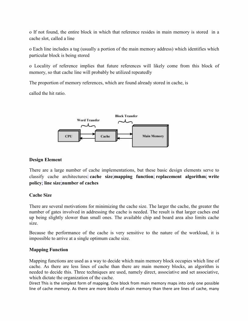
o If not found, the entire block in which that reference resides in main memory is stored in a cache slot, called a line
o Each line includes a tag (usually a portion of the main memory address) which identifies which particular block is being stored
o Locality of reference implies that future references will likely come from this block of memory, so that cache line will probably be utilized repeatedly
The proportion of memory references, which are found already stored in cache, is
called the hit ratio.
Design Element
There are a large number of cache implementations, but these basic design elements serve to classify cache architectures: cache size;mapping function; replacement algorithm; write policy; line size;number of caches
Cache Size
There are several motivations for minimizing the cache size. The larger the cache, the greater the number of gates involved in addressing the cache is needed. The result is that larger caches end up being slightly slower than small ones. The available chip and board area also limits cache size.
Because the performance of the cache is very sensitive to the nature of the workload, it is impossible to arrive at a single optimum cache size.
Mapping Function
Mapping functions are used as a way to decide which main memory block occupies which line of cache. As there are less lines of cache than there are main memory blocks, an algorithm is needed to decide this. Three techniques are used, namely direct, associative and set associative, which dictate the organization of the cache. Direct This is the simplest form of mapping. One block from main memory maps into only one possible line of cache memory. As there are more blocks of main memory than there are lines of cache, many
blocks in main memory can map to the same line in cache memory. To implement this function, use the following formula: α = β % γ where α is the cache line number, β is the block number in main memory, γ is the total number of lines in cache memory and % being the modulus operator. The main disadvantage of using this type of mapping is that there is a fixed cache location for any given block in main memory. If two blocks of memory sharing the same cache line are being continually referenced, cache misses would occur and these two blocks would continuously be swapped, resulting in slower memory access due to the time taken to access main memory (or the next level of memory). Associative This type of mapping overcomes the disadvantage of direct mapping by permitting each main memory block to be loaded into any line of cache. To do so, the cache control logic interprets a memory address as a tag and a word field. The tag uniquely identifies a block in main memory. The primary disadvantage of this method is that to find out whether a particular block is in cache, all cache lines would have to be examined. Using this method, replacement algorithms are required to maximize its potential. Set Associative This type of mapping is designed to utilize the strengths of the previous two mappings, while minimizing the disadvantages. The cache is divided into a number of sets containing an equal number of lines. Each block in main memory maps into one set in cache memory similar to that of direct mapping. Within the set, the cache acts as associative mapping where a block can occupy any line within that set. Replacement algorithms may be used within the set.
Replacement Algorithms
For direct mapping where there is only one possible line for a block of memory, no replacement algorithm is needed. For associative and set associative mapping, however, an algorithm is needed. For maximum speed, this algorithm is implemented in the hardware. Four of the most common algorithms are: least recently used This replaces the candidate line in cache memory that has been there the longest
with no reference to it. first in first out This replaces the candidate line in the cache that has been there
the longest. least frequently used This replaces the candidate line in the cache that has had the fewest
references. random replacement This algorithm randomly chooses a line to be replaced from among the
candidate lines. Studies have shown that this yields only slightly inferior performance than other
algorithms.
Write Policy
This is important because if changes were made to a line in cache memory, the appropriate changes should be made to the block in main memory before removing the line from the cache. The problems to contend with are more than one device may have access to main memory (I/O modules). If more than one processor on the same bus with its own cache is involved, the problem becomes more complex. Any change in either cache or main memory could invalidate the others.
The simplest technique is called ―write through‖. In using this technique, both main memory and cache are written to when a write operation is performed, ensuring that main memory is always valid. The main disadvantage of this technique is that it may generate substantial main memory traffic, causing a bottle neck and decreasing performance. An alternative technique, known as ―write back‖ minimizes main memory writes. Updates are made only in the cache. An update bit associated with the line is set. Main memory is updated when the line in cache gets replaces only if the update bit has been set. The problem with this technique is that all changes to main memory have to be made through the cache in order not to invalidate parts of main memory, which potentially may cause a bottle neck.
Line Size
When a block of data is retrieved from main memory and put into the cache, the desired word and a number of adjacent words are retrieved. As the block size increases from a very small size, the hit ratio will at first increase due to the principle of locality of reference, which says that words in the vicinity of a referenced word are more likely to be referenced in the near future. As the block size increases, however, the hit ratio will decrease as the probability of reusing the new informationbecomes less than that of using the information that has been replaced.
2.17.Memory System of Micro-Computers A microcomputer is a small, relatively inexpensive computer with a microprocessor as its central processing unit (CPU). It includes a microprocessor, memory, and input/output (I/O) facilities. Microcomputers became popular in the 1970s and 80s with the advent of increasingly powerful microprocessors. The predecessors to these computers, mainframes and minicomputers, were comparatively much larger and more expensive (though indeed present-day mainframes such as the IBM System z machines use one or more custom microprocessors as their CPUs). Many microcomputers (when equipped with a keyboard and screen for input and output) are alsopersonal computers (in the generic sense).
The term microcomputer came into popular use after the introduction of the minicomputer, although Isaac Asimov used the term microcomputer in his short story "The Dying Night" as early as 1956 (published in The Magazine of Fantasy and Science Fiction in July that year). Most notably, the microcomputer replaced the many separate components that made up the minicomputer's CPU with one integrated microprocessor chip. The French developers of the Micral N (1973) filed their patents with the term "Micro-ordinateur", a literal equivalent of "Microcomputer", to designate the first solid state machine designed with a microprocessor. In the USA, the earliest models such as the Altair 8800 were often sold as kits to be assembled by the user, and came with as little as 256 bytes of RAM, and no input/output devices other than indicator lights and switches, useful as a proof of concept to demonstrate what such a simple device could do. However, as microprocessors and semiconductor memory became less expensive, microcomputers in turn grew cheaper and easier to use:
Increasingly inexpensive logic chips such as the 7400 series allowed cheap dedicated circuitry for improved user interfaces such as keyboard input, instead of simply a row of switches to toggle bits one at a time.
Use of audio cassettes for inexpensive data storage replaced manual re-entry of a program every time the device was powered on.
Large cheap arrays of silicon logic gates in the form of Read-only memory and EPROMs allowed utility programs and self-booting kernels to be stored within microcomputers. These stored programs could automatically load further more complex software from external storage devices without user intervention, to form an inexpensive turnkey system that does not require a computer expert to understand or to use the device.
Random access memory became cheap enough to afford dedicating approximately 1-2 kilobytes of memory to a video display controller frame buffer, for a 40x25 or 80x25 text display or blocky color graphics on a common household television. This replaced the slow, complex, and expensive teletypewriter that was previously common as an interface to minicomputers and mainframes.
All these improvements in cost and usability resulted in an explosion in their popularity during the late 1970s and early 1980s. A large number of computer makers packaged microcomputers for use in small business applications. By 1979, many companies such as Cromemco, Processor Technology, IMSAI, North Star Computers, Southwest Technical Products Corporation, Ohio Scientific, Altos, Morrow Designs and others produced systems designed either for a resourceful end user or consulting firm to deliver business systems such as accounting, database management, and word processing to small businesses. This allowed businesses unable to afford leasing of a minicomputer or time-sharing service the opportunity to automate business functions, without (usually) hiring a full-time staff to operate the computers. A representative system of this era would have used an S100 bus, an 8-bit processor such as an Intel 8080 or Zilog Z80, and either CP/M or MP/M operating system. The increasing availability and power of desktop computers for personal use attracted the attention of more software developers. In time, and as the industry matured, the market for personal computers standardized around IBM PC compatibles running DOS, and later Windows. Modern desktop computers, video game consoles, laptops,tablet PCs, and many types of handheld devices, including mobile phones, pocket calculators, and industrial embedded systems, may all be considered examples of microcomputers according to the definition given above.
2.18.Input/ Output System A general purpose computer should have the ability to exchange information with a wide range of devices in varying environments. Computers can communicate with other computers over the Internet and access information around the globe. They are an integral part of home appliances, manufacturing equipment, transportation systems, banking and point-of-sale terminals. In this chapter, we study the various ways in which I/O operations are performed.
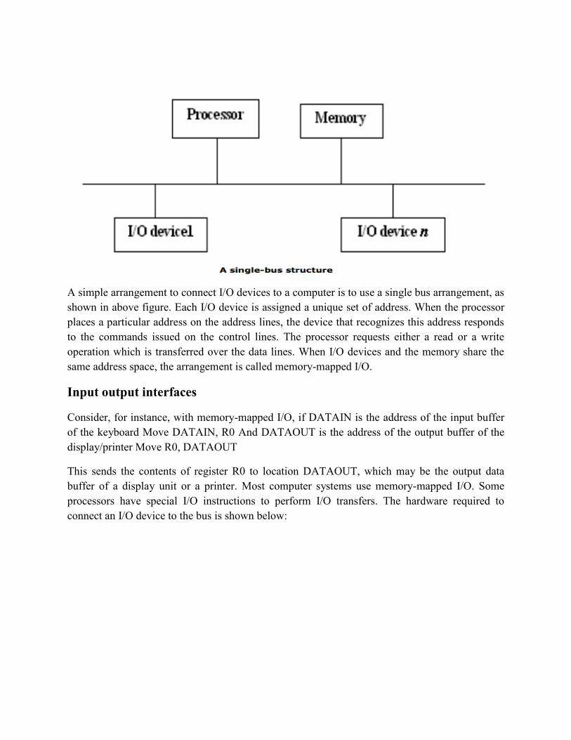
A simple arrangement to connect I/O devices to a computer is to use a single bus arrangement, as shown in above figure. Each I/O device is assigned a unique set of address. When the processor places a particular address on the address lines, the device that recognizes this address responds to the commands issued on the control lines. The processor requests either a read or a write operation which is transferred over the data lines. When I/O devices and the memory share the same address space, the arrangement is called memory-mapped I/O.
Input output interfaces
Consider, for instance, with memory-mapped I/O, if DATAIN is the address of the input buffer of the keyboard Move DATAIN, R0 And DATAOUT is the address of the output buffer of the display/printer Move R0, DATAOUT
This sends the contents of register R0 to location DATAOUT, which may be the output data buffer of a display unit or a printer. Most computer systems use memory-mapped I/O. Some processors have special I/O instructions to perform I/O transfers. The hardware required to connect an I/O device to the bus is shown below:
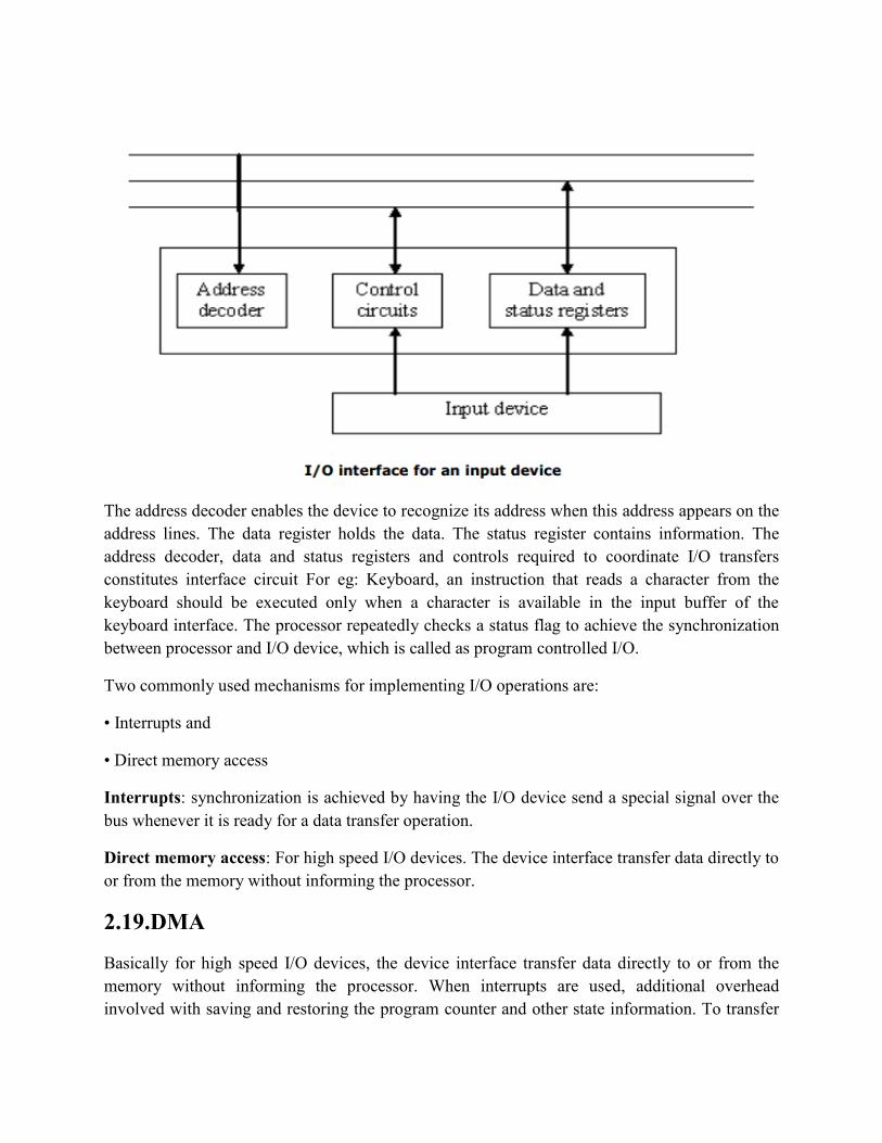
The address decoder enables the device to recognize its address when this address appears on the address lines. The data register holds the data. The status register contains information. The address decoder, data and status registers and controls required to coordinate I/O transfers constitutes interface circuit For eg: Keyboard, an instruction that reads a character from the keyboard should be executed only when a character is available in the input buffer of the keyboard interface. The processor repeatedly checks a status flag to achieve the synchronization between processor and I/O device, which is called as program controlled I/O.
Two commonly used mechanisms for implementing I/O operations are:
• Interrupts and
• Direct memory access
Interrupts: synchronization is achieved by having the I/O device send a special signal over the bus whenever it is ready for a data transfer operation.
Direct memory access: For high speed I/O devices. The device interface transfer data directly to or from the memory without informing the processor.
2.19.DMA
Basically for high speed I/O devices, the device interface transfer data directly to or from the memory without informing the processor. When interrupts are used, additional overhead involved with saving and restoring the program counter and other state information. To transfer
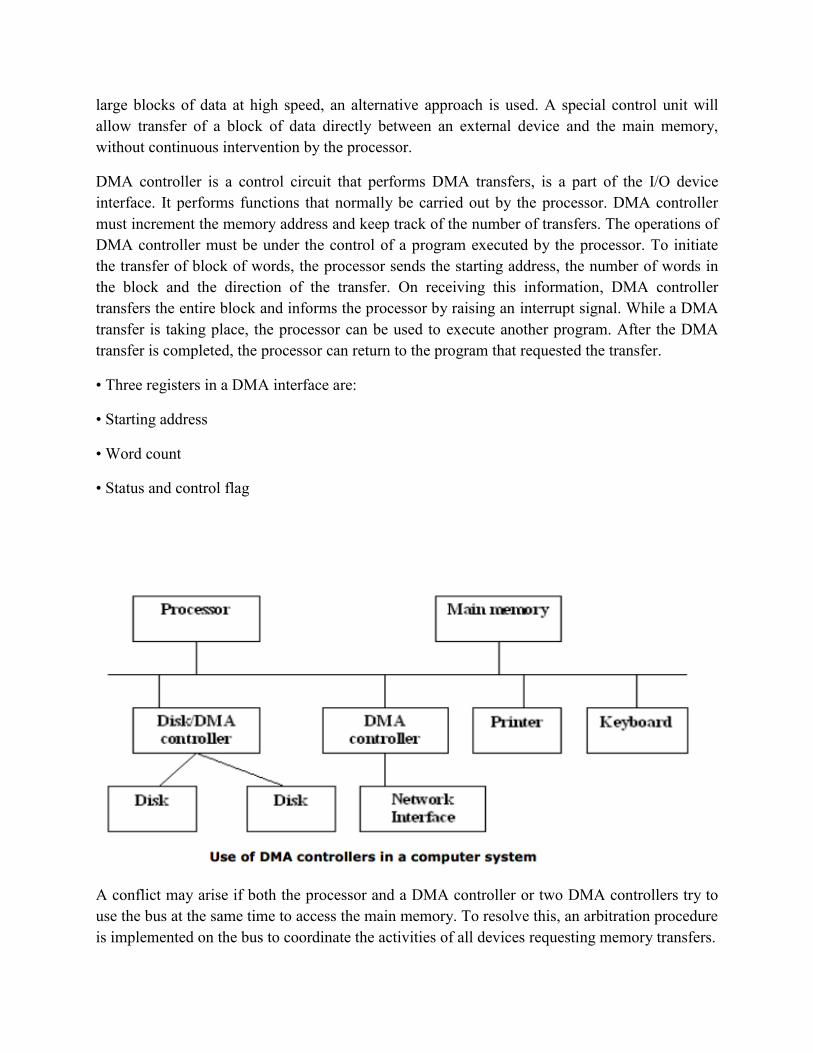
large blocks of data at high speed, an alternative approach is used. A special control unit will allow transfer of a block of data directly between an external device and the main memory, without continuous intervention by the processor.
DMA controller is a control circuit that performs DMA transfers, is a part of the I/O device interface. It performs functions that normally be carried out by the processor. DMA controller must increment the memory address and keep track of the number of transfers. The operations of DMA controller must be under the control of a program executed by the processor. To initiate the transfer of block of words, the processor sends the starting address, the number of words in the block and the direction of the transfer. On receiving this information, DMA controller transfers the entire block and informs the processor by raising an interrupt signal. While a DMA transfer is taking place, the processor can be used to execute another program. After the DMA transfer is completed, the processor can return to the program that requested the transfer.
• Three registers in a DMA interface are:
• Starting address
• Word count
• Status and control flag
A conflict may arise if both the processor and a DMA controller or two DMA controllers try to use the bus at the same time to access the main memory. To resolve this, an arbitration procedure is implemented on the bus to coordinate the activities of all devices requesting memory transfers.
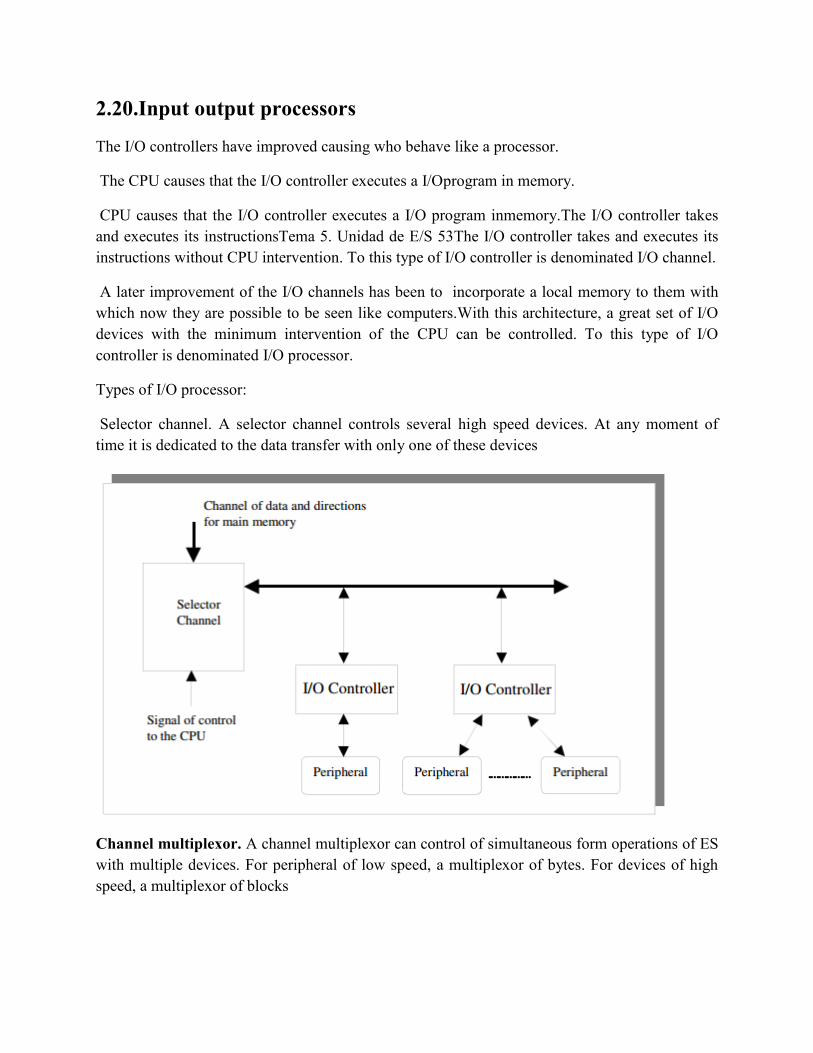
2.20.Input output processors
The I/O controllers have improved causing who behave like a processor.
The CPU causes that the I/O controller executes a I/Oprogram in memory.
CPU causes that the I/O controller executes a I/O program inmemory.The I/O controller takes and executes its instructionsTema 5. Unidad de E/S 53The I/O controller takes and executes its instructions without CPU intervention. To this type of I/O controller is denominated I/O channel.
A later improvement of the I/O channels has been to incorporate a local memory to them with which now they are possible to be seen like computers.With this architecture, a great set of I/O devices with the minimum intervention of the CPU can be controlled. To this type of I/O controller is denominated I/O processor.
Types of I/O processor:
Selector channel. A selector channel controls several high speed devices. At any moment of time it is dedicated to the data transfer with only one of these devices
Channel multiplexor. A channel multiplexor can control of simultaneous form operations of ES with multiple devices. For peripheral of low speed, a multiplexor of bytes. For devices of high speed, a multiplexor of blocks
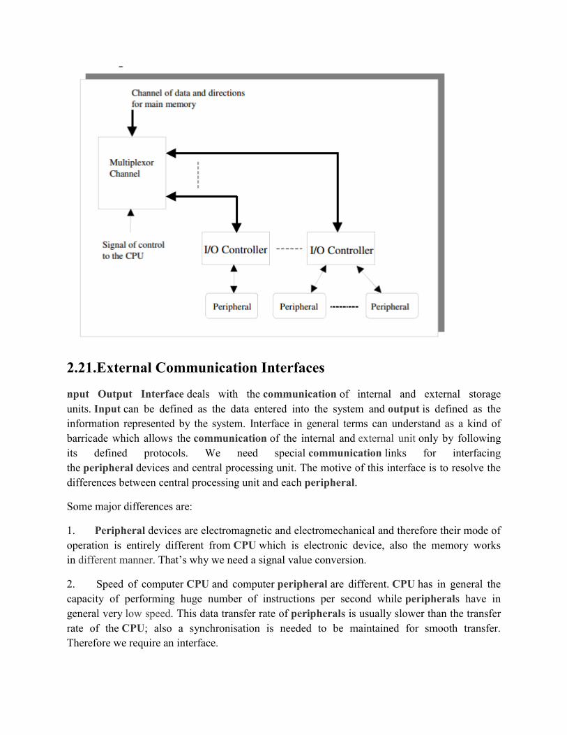
2.21.External Communication Interfaces
nput Output Interface deals with the communication of internal and external storage units. Input can be defined as the data entered into the system and output is defined as the information represented by the system. Interface in general terms can understand as a kind of barricade which allows the communication of the internal and external unit only by following its defined protocols. We need special communication links for interfacing the peripheral devices and central processing unit. The motive of this interface is to resolve the differences between central processing unit and each peripheral.
Some major differences are:
1. Peripheral devices are electromagnetic and electromechanical and therefore their mode of operation is entirely different from CPU which is electronic device, also the memory works in different manner. That‘s why we need a signal value conversion.
2. Speed of computer CPU and computer peripheral are different. CPU has in general the capacity of performing huge number of instructions per second while peripherals have in general very low speed. This data transfer rate of peripherals is usually slower than the transfer rate of the CPU; also a synchronisation is needed to be maintained for smooth transfer. Therefore we require an interface.
3. The data codes and format of the peripherals is different from the word format in the CPU and memory.
4. The speed and operating mode of different peripheral also differs, so as to synchronise the different peripheral among them and also with the CPU interfaces are designed.
For homework help and assignment help contact our experts on Transtutors.com. We have a dedicated team to resolve all your doubts and will also try to explain it from the scratch. We cover subject from school, under graduate and graduate level in almost all discipline.
To resolve these differences, computer system need to include special hardware component between the CPU and peripherals to synchronise, supervise and guide the input – output transfers between the peripheral and memory. These components are termed as interface because they interface between peripheral and processor bus. In addition to these each peripheral can have its own separate interface to synchronise and supervise its own controller.
The input-output bus from the processor is attached to all the peripherals interfaces to communicate. To communicate with each peripheral device separately the processor places the device address on the address line. Each interface attached to the input-output bus contains a decoder which decodes the address from address line and places it correctly. When the decoder senses that the address belongs to its peripheral device then the link between the bus lines and the device that it controls is activated. Rest all whose match is not found remain deactivated.
Processor provides function code in these control lines. The interface selected responds to the function code and executes it and then move forward onto the next.
For more help log on to Transtutors.com. Our experts also provide homework help and assignment help. We are very punctual for the timings and specifications laid by you. We cover a wide range of topics from school to graduate level. Our sincere and dedicated team will look forward your each and every doubt even after the completion of you assignment if you found so.
2.22.Interrupt Processing
There are many situations where other tasks can be performed while waiting for an I/O device to become ready. A hardware signal called an Interrupt will alert the processor when an I/O device becomes ready. Interrupt-request line is usually dedicated for this purpose. For example, consider, COMPUTE and PRINT routines. The routine executed in response to an interrupt request is called interrupt-service routine. Transfer of control through the use of interrupts happens. The processor must inform the device that its request has been recognized by sending interrupt-acknowledge signal. One must therefore know the difference between Interrupt Vs Subroutine. Interrupt latency is concerned with saving information in registers will increase the
delay between the time an interrupt request is received and the start of execution of the interrupt-service routine.
Interrupt hardware Most computers have several I/O devices that can request an interrupt. A single interrupt request line may be used to serve n devices. Enabling and Disabling Interrupts All computers fundamentally should be able to enable and disable interruptions as desired. Again reconsider the COMPUTE and PRINT example. When a device activates the interrupt-request signal, it keeps this signal activated until it learns that the processor has accepted its request. When interrupts are enabled, the following is a typical scenario:
• The device raises an interrupt request.
• The processor interrupts the program currently being executed.
• Interrupts are disabled by changing the control bits in the processor status register (PS).
• The device is informed that its request has been recognized and deactivates the interrupt request signal.
• The action requested by the interrupt is performed by the interrupt-service routine.
• Interrupts are enabled and execution of the interrupted program is resumed. Handling multiple devices While handling multiple devices, the issues concerned are:
• How can the processor recognize the device requesting an interrupt?
• How can the processor obtain the starting address of the appropriate routine?
• Should a device be allowed to interrupt the processor while another interrupt is being serviced?
• How should two or more simultaneous interrupt requests be handled?
Vectored interrupts -A device requesting an interrupt may identify itself (by sending a special code) directly to the processor, so that the processor considers it immediately
Interrupt nesting The processor should continue to execute the interrupt-service routine till completion, before it accepts an interrupt request from a second device. Privilege exception means they execute privileged instructions. Individual interrupt-request and acknowledge lines can also be implemented. Implementation of interrupt priority using individual interrupt-request and acknowledge lines has been shown in figure
Simultaneous requests The processor must have some mechanisms to decide which request to service when simultaneous requests arrive. Here, daisy chain and arrangement of priority groups as the interrupt priority schemes are discussed. Priority based simultaneous requests are considered in many organizations.
Controlling device requests At the device end, an interrupt enable bit determines whether it is allowed to generate an interrupt request. At the processor end, it determines whether a given interrupt request will be accepted.
Exceptions The term exception is used to refer to any event that causes an interruption. Hence, I/O interrupts are one example of an exception.
• Recovery from errors – These are techniques to ensure that all hardware components are operating properly.
• Debugging – find errors in a program, trace and breakpoints (only at specific points selected by the user).
• Privilege exception – execute privileged instructions to protect OS of a computer.
Use of interrupts in Operating Systems Operating system is system software which is also termed as resource manager, as it manages all variety of computer peripheral devices efficiently. Different issues addressed by the operating systems are: Assign priorities among jobs, Security and protection features, incorporate interrupt-service routines for all devices and Multitasking, time slice, process, program state, context switch and others.
2.23.BUS arbitration
The device that is allowed to initiate data transfers on the bus at any given time is called the bus master. Arbitration is the process by which the next device to become the bus master is selected and bus mastership is transferred to it. The two approaches are centralized and distributed arbitrations. In centralized, a single bus arbiter performs the required arbitration whereas in distributed, all device participate in the selection of the next bus master. The bus arbiter may be the processor or a separate unit connected to the bus. The processor is normally the bus master unless it grants bus mastership to one of the DMA controllers. A simple arrangement for bus arbitration using daisy chain and a distributed arbitration scheme
In Centralized arbitration, A simple arrangement for bus arbitration using a daisy chain shows the arbitration solution. A rotating priority scheme may be used to give all devices an equal chance of being serviced (BR1 to BR4). In Distributed arbitration, all devices waiting to use the bus have equal responsibility in carrying out the arbitration process, without using a central arbiter. The drivers are of the open-collector type. Hence, if the input to one driver is equal to 1 and the input to another driver connected to the same bus line is equal to 0 the bus will be in the low-voltage state. This uses ARB0 to ARB3.
2.24.Floppy Drives
A floppy disk, or diskette, is a disk storage medium composed of a disk of thin and flexible magnetic storage medium, sealed in a rectangular plastic carrier lined with fabric that removes dust particles. They are read and written by a floppy disk drive (FDD).
Floppy disks, initially as 8-inch (200 mm) media and later in 5.25-inch (133 mm) and 3.5-inch (90 mm) sizes, were a ubiquitous form of data storage andexchange from the mid-1970s well into the first decade of the 21st century.[1]
By 2010, computer motherboards were rarely manufactured with floppy drive support; 3 1⁄2-inch floppies could be used as an external USB drive, but5 1⁄4-inch, 8-inch, and non-standard drives could only be handled by old equipment.
While floppy disk drives still have some limited uses, especially with legacy industrial computer equipment, they have been superseded by data storage methods with much greater capacity, such as USB flash drives, portable external hard disk drives, optical discs, memory cards, and computer networks.
The earliest floppy disks, developed in the late 1960s, were 8 inches (200 mm) in diameter;[1] they became commercially available in 1971.[2] These disks and associated drives were produced and improved upon by IBM and other companies such as Memorex, Shugart Associates, and Burroughs Corporation. The phrase "floppy disk" appeared in print as early as 1970, and although in 1973 IBM announced its first media as "Type 1 Diskette" the industry continued to use the terms "floppy disk" or "floppy".
In 1976, Shugart Associates introduced the first 5 1⁄4-inch FDD. By 1978 there were more than 10 manufacturers producing such FDDs. There were competing floppy disk formats, with hard and soft sectorversions and encoding schemes such as FM, MFM and GCR. The 5¼ inch format displaced the 8-inch one for most applications, and the hard sectored disk format disappeared. In 1984, IBM introduced the 1.2 MB dual sided floppy disk along with its AT model. IBM started using the 720 KB double density 3.5-inch microfloppy disk on its Convertible laptop computer in 1986 and the 1.44 MB high density version with thePS/2 line in 1987. These disk drives could be added to older PC models. In 1988 IBM introduced a drive for 2.88 MB "DSED" diskettes in its top-of-the-line PS/2 models but this was a commercial failure.
Throughout the early 1980s, limitations of the 5 1⁄4-inch format became clear. Originally designed to be more practical than the 8-inch format, it was itself too large; as the quality of recording media grew, data could be stored in a smaller area.[5] A number of solutions were developed, with drives at 2, 2 1⁄2, 3 and 3 1⁄2 inches (and Sony's 90.0 mm × 94.0 mm disk) offered by various companies. They all shared a number of advantages over the old format, including a rigid case with a sliding write protection tab, protecting them from damage; the large market share of the5 1⁄4-inch format made it difficult for these new formats to gain significant market share.[5] A variant on the Sony design, introduced in 1982 by a large number of manufacturers, was then rapidly adopted; by 1988 the 3 1⁄2-inch was outselling the 5 1⁄4-inch.
By the end of the 1980s, the 5 1⁄4-inch disks had been superseded by the 3 1⁄2-inch disks. By the mid-1990s, the 5 1⁄4-inch drives had virtually disappeared as the 3 1⁄2-inch disk became the
predominant floppy disk. The advantages of the 3 1⁄2-inch disk were its smaller size and its plastic case which provided better protection from dirt and other environmental risks while the 5 1⁄4-inch disk was available cheaper per piece throughout its history, usually with a price in the range of one third to two thirds of a 3 1⁄2-inch disk
2.25.CD-ROM A CD-ROM /ˌsiːˌdiːˈrɒm/ is a pre-pressed compact disc which contains data. The name is an acronym which stands for "Compact Disc Read-Only Memory". Computers can read CD-ROMs, but cannot write on them.
CD-ROMs are popularly used to distribute computer software, including video games and multimedia applications, though any data can be stored (up to the capacity limit of a disc). Some CDs, called enhanced CDs, hold both computer data and audio with the latter capable of being played on a CD player, while data (such as software or digital video) is only usable on a computer (such as ISO 9660 format PC CD-ROMs).
The Yellow Book is the technical standard that defines the format of CD-ROMs. One of a set of color-bound books that contain the technical specifications for all CD formats, the Yellow Book, created by Sony and Philips in 1988, was the first extension of Compact Disc Digital Audio. It adapted the format to hold any form of data.
CD-ROM drives
CD-ROM discs are read using CD-ROM drives. A CD-ROM drive may be connected to the computer via an IDE (ATA), SCSI, SATA, FireWire, or USBinterface or a proprietary interface, such as the Panasonic CD interface. Virtually all modern CD-ROM drives can also play audio CDs (as well as Video CDs and other data standards) when used in conjunction with the right software.
Laser and optics CD-ROM drives employ a near-infrared 780 nm laser diode. The laser beam is directed onto the disc via an opto-electronic tracking module, which then detects whether the beam has been reflected or scattered. Transfer rates CD-ROM drives are rated with a speed factor relative to music CDs. If a CD-ROM is read at the same rotational speed as an audio CD, the data transfer rate is 150 KiB/s, commonly referred to as "1×". At this data rate, the track moves along under the laser spot at about 1.2 m/s. To maintain this linear velocity as the optical head moves to different positions, the angular velocity is varied from 500 rpm at the inner edge to 200 rpm at the outer edge. The 1× speed rating for CD-ROM (150 KiB/s) is different than the 1× speed rating for DVDs (1.32 MiB/s).
Copyright issues
Software distributors, and in particular distributors of computer games, often make use of various copy protection schemes to prevent software running from any media besides the original CD-ROMs. This differs somewhat from audio CD protection in that it is usually implemented in both the media and the software itself. The CD-ROM itself may contain "weak" sectors to make copying the disc more difficult, and additional data that may be difficult or impossible to copy to a CD-R or disc image, but which the software checks for each time it is run to ensure an original disc and not an unauthorized copy is present in the computer's CD-ROM drive.Manufacturers of CD writers (CD-R or CD-RW) are encouraged by the music industry to ensure that every drive they produce has a unique identifier, which will be encoded by the drive on every disc that it records: the RID or Recorder Identification Code.[11] This is a counterpart to the Source Identification Code (SID), an eight character code beginning with "IFPI" that is usually stamped on discs produced by CD recording plants.
2.26.DVD-ROM DVD is a digital optical disc storage format, invented and developed by Philips, Sony, Toshiba, and Panasonic in 1995. DVDs offer higher storage capacity than compact discs while having the same dimensions.
Pre-recorded DVDs are mass-produced using molding machines that physically stamp data onto the DVD. Such discs are known as DVD-ROM, because data can only be read and not written or erased. Blank recordable DVD discs (DVD-R and DVD+R) can be recorded once using a DVD recorder and then function as a DVD-ROM. Rewritable DVDs (DVD-RW, DVD+RW, and DVD-RAM) can be recorded and erased multiple times.
DVDs are used in DVD-Video consumer digital video format and in DVD-Audio consumer digital audio format, as well as for authoring AVCHD discs. DVDs containing other types of information may be referred to as DVD data discs.
DVD drives and players
DVD drives are devices that can read DVD discs on a computer. DVD players are a particular type of devices that do not require a computer to work, and can read DVD-Video and DVD-Audiodiscs
Laser and optics DVD uses 650 nm wavelength laser diode light, as opposed to 780 nm for CD. This shorter wavelength etches a smaller pit on the media surface compared to CDs (0.74 µm for DVD versus 1.6 µm for CD), allowing in part for DVD's increased storage capacity.
In comparison, Blu-ray Disc, the successor to the DVD format, uses a wavelength of 405 nm, and one dual-layer disc has a 50 GB storage capacity.
Transfer rates
Read and write speeds for the first DVD drives and players were of 1,385 kB/s (1,353 KiB/s); this speed is usually called "1×". More recent models, at 18× or 20×, have 18 or 20 times that speed. Note that for CD drives, 1× means 153.6 kB/s (150 KiB/s), about one-ninth as swift
Zip The Zip drive is a medium-capacity removable disk storage system that was introduced by Iomega in late 1994. Originally, Zip disks launched with capacities of 100 MB, but later versions increased this to first 250 MB and then 750 MB.
The format became the most popular of the super-floppy type products which filled a niche in the late 1990s portable storage market. However it was never popular enough to replace the 3.5-inch floppy disk nor could ever match the storage size available on rewritable CDs and later rewritable DVDs.USB flash drives ultimately proved to be the better rewritable storage medium among the general public due to the near-ubiquity of USB ports on personal computers and soon after because of the far greater storage sizes offered. Zip drives fell out of favor for mass portable storage during the early 2000s. The Zip brand later covered internal and external CD writers known as Zip-650 or Zip-CD, which had no relation to the Zip drive.
Jaz The Jaz drive was a removable disk storage system introduced by the Iomega company in 1995. The system has since been discontinued. The Jaz disks were originally released with a 1 GB capacity (there was also 540 MB, but it was unreleased) in a 3½-inch form factor; its capacity was a significant increase over Iomega's most popular product at the time, the Zip drive, with its 100 MB capacity. The Jaz drive used only the SCSI interface (the IDE internal version is rare), but an adapter known as Jaz Traveller was available to connect it to a standard parallel port. The capacity was later increased to 2 GB, through a drive and disk revision in 1998, before the Jaz line was ultimately discontinued in 2002.
Problems
The Jaz drive was less prone to failure than was the Zip drive. Even so, earlier Jaz drives could overheat, and loading-mechanism jams could leave a cartridge stuck in the drive. Forcibly ejecting a stuck cartridge could destroy both drive and cartridge. Jaz drives were based on hard-disk technology, making them susceptible to contaminants in the drive; dust and grit could be introduced through a hole in the cartridge where the motor drove the platters, and any dust built up on the external case could enter the drive with its next insertion. Additionally, the metal sliding door was capable of wearing the plastic, resulting in debris and head crashes.
Furthermore, the mechanism used to attach the platters to the spindle motor was complex and tended to vibrate noisily. Iomega implemented an anti-gyro device (much like an optical CD/DVD drive) within the cartridge to prevent vibration at spin-up, but this device lost effectiveness with age. As a result, the two platters could lose alignment, rendering the cartridge unusable. The plastic gears attached to the bottom of a Jaz cartridge often stripped and broke, rendering the inserted disk physically incapable of spinning up to operating speed.
2.27.Cartridge Drives Disk Cartridge Disk cartridge or Optical disk cartridge may refer to:
A 1960s computer disk pack which has a single hard disk platter encased in a protective plastic shell
Removable disk storage media Zip disk A 31
⁄2-inch Floppy disk An optical disc or magneto-optical disc enclosed in a protective plastic sheath called
a Caddy (hardware) Ultra Density Optical Universal Media Disc Disk enclosure ROM cartridge
Tape Drive A tape drive is a data storage device that reads and writes data on a magnetic tape. Magnetic tape data storage is typically used for offline, archival data storage. Tape media generally has a favorable unit cost and long archival stability.
A tape drive provides sequential access storage, unlike a disk drive, which provides random access storage. A disk drive can move to any position on the disk in a few milliseconds, but a tape drive must physically wind tape between reels to read any one particular piece of data. As a result, tape drives have very slow average seek times. For sequential access once the tape is positioned, however, tape drives can stream data very fast. For example, as of 2010 Linear Tape-Open (LTO) supported continuous data transfer rates of up to 140 MB/s, comparable to hard disk drives.
ROM Cartridge A ROM cartridge, sometimes referred to simply as a cartridge or cart, is a removable enclosure containing read-only memory devices designed to be connected to a consumer electronics device such as a home computer or games console. ROM cartridges can be used to load software such as video games, or other application programs.
The cartridge slot could be used for hardware additions, for example speech synthesis. Some cartridges had battery-backed static random-access memory, allowing a user to save data such as game scores between uses.
ROM cartridges allowed the user to rapidly load and access programs and data without the expense of a floppy disk drive, which was an expensive peripheral during the home computer era, and without using slow, sequential, and often unreliable Compact Cassette tape. An
advantage for the manufacturer was the relative security of distribution of software in cartridge form, which was difficult for end users to replicate. However, cartridges were expensive to manufacture compared to making a floppy disk or CD-ROM. As disk drives became more common and software expanded beyond the practical limits of ROM size, cartridge slots disappeared from later consoles and computers. Cartridges are still used today with handheld gaming consoles such as Nintendo 3DS and PlayStation Vita.
2.28.Recordable CDs A CD-R (Compact Disc-Recordable) is a variation of the compact disc invented by Philips and Sony. CD-R is a Write Once Read Many (WORM) optical medium, although the whole disk does not have to be entirely written in the same session.
CD-R retains a high level of compatibility with standard CD readers, unlike CD-RW which can be re-written, but is not capable of playing on many readers.
Writing Method
The blank disc has a pre-groove track onto which the data are written. The pre-groove track, which also contains timing information, ensures that the recorder follows the same spiral path as a conventional CD. A CD recorder writes data to a CD-R disc by pulsing its laser to heat areas of the organic dye layer. The writing process does not produce indentations (pits); instead, the heat permanently changes the optical properties of the dye, changing the reflectivity of those areas. Using a low laser power, so as not to further alter the dye, the disc is read back in the same way as a CD-ROM. However, the reflected light is modulated not by pits, but by the alternating regions of heated and unaltered dye. The change of the intensity of the reflected laser radiation is transformed into an electrical signal, from which the digital information is recovered ("decoded"). Once a section of a CD-R is written, it cannot be erased or rewritten, unlike a CD-RW. A CD-R can be recorded in multiple sessions. A CD recorder can write to a CD-R using several methods including:
1. Disc At Once – the whole CD-R is written in one session with no gaps and the disc is "closed" meaning no more data can be added and the CD-R effectively becomes a standard read-only CD. With no gaps between the tracks the Disc At Once format is useful for "live" audio recordings.
2. Track At Once – data are written to the CD-R one track at a time but the CD is left "open" for further recording at a later stage. It also allows data and audio to reside on the same CD-R.
3. Packet Writing – used to record data to a CD-R in "packets", allowing extra information to be appended to a disc at a later time, or for information on the disc to be made "invisible". In this way, CD-R can emulate CD-RW; however, each time information on the disc is altered, more data has to be written to the disc. There can be compatibility issues with this format and some CD drives.
With careful examination, the written and unwritten areas can be distinguished by the naked eye. CD-Rs are written from the center outwards, so the written area appears as an inner band with slightly different shading.
2.29.CD-RW A CD-RW (Compact Disc-ReWritable) is a rewritable optical disc. It was introduced in 1997, and was known as "CD-Writable" during development. It was preceded by the CD-MO, which was never commercially released.
CD-RW disc require a more sensitive laser optics. Also, CD-RWs cannot be read in some CD-ROM drives built prior to 1997. CD-ROM drives will bear a "MultiRead" certification to show compatibility. CD-RW discs need to be blanked before reuse. Different blanking methods can be used, including "full" blanking in which the entire surface of the disc is cleared, and "fast" blanking in which only meta-data areas are cleared: PMA, TOC and pregap, comprising a few percent of the disc. Fast blanking is much quicker, and is usually sufficient to allow rewriting the disc. Full blanking removes traces of the former data, often for confidentiality. It may be possible to recover data from full-blanked CD-RWs with specialty data recovery equipment[citation needed]; however, this is generally not used except by government agencies due to cost.
CD-RW also have a shorter rewriting cycles life (ca. 1,000) compared to virtually all of the previously exposed types storage of media (typically well above 10,000 or even 100,000), something which however is less of a drawback considering that CD-RWs are usually written and erased in their totality, and not with repeated small scale changes, so normally wear leveling is not an issue.
Their ideal usage field is in the creation of test disks, temporary short or mid-term backups, and in general, where an intermediate solution between online and offline storage schemes is required.
2.30.Input/ Output Technologies input/output device, also known as computer peripheral, any of various devices (including sensors) used to enter information and instructions into a computer for storage or processing and to deliver the processed data to a human operator or, in some cases, a machine controlled by the computer. Such devices make up the peripheral equipment of modern digital computer systems.
An input device converts incoming data and instructions into a pattern of electrical signals in binarycode that are comprehensible to a digital computer. An output device reverses the process, translating the digitized signals into a form intelligible to the user. At one time punched-card and paper-tape readers were extensively used for inputting, but these have now been supplanted by more efficient devices.
Input devices include typewriter-like keyboards; handheld devices such as the mouse, trackball, joystick, and special pen with pressure-sensitive pad; and microphones. They also include
sensors that provide information about their environment—temperature, pressure, and so forth—
to a computer. Another direct-entry mechanism is the optical laser scanner (e.g., scanners used with point-of-sale terminals in retail stores) that can read bar-coded data or optical character fonts. Output equipment includes video display terminals (either cathode-ray tubes or liquid crystal displays), ink-jet and laser printers, loudspeakers, and devices such as flow valves that control machinery, often in response to computer processing of sensor input data. Some devices, such as video display terminals, may provide both input and output. Other examples are devices that enable the transmission and reception of data between computers—e.g., modems and network interfaces. Most auxiliary storage devices—as, for example, magnetic tape, magnetic disk drives, and certain types of optical compact discs—also double as input/output devices (see computer memory).
Various standards for connecting peripherals to computers exist. For example, integrated drive electronics (IDE) and enhanced integrated drive electronics (EIDE) are common interfaces, or buses, for magnetic disk drives. A bus (also known as a port) can be either serial or parallel, depending on whether the data path carries one bit at a time (serial) or many at once (parallel). Serial connections, which use relatively few wires, are generally simpler and slower than parallel connections. Universal serial bus (USB) is a common serial bus. A common example of a parallel bus is the small computer systems interface, or SCSI, bus.
2.31.Characteristics
SPEED : In general, no human being can compete to solving the complex computation, faster than computer.
ACCURACY : Since Computer is programmed, so what ever input we give it gives result with accuratly.
STORAGE : Computer can store mass storage of data with appropriate formate.
DILIGENCE : Computer can work for hours without any break and creating error.
VERSATILITY : We can use computer to perform completely different type of work at the same time.
POWER OF REMEMBERING : It can remember data for us.
NO IQ : Computer does not work without instruction.
NO FEELING : Computer does not have emotions, knowledge, experience, feeling.
2.32.Video Cards A video card (also called a video adapter, display card, graphics card, graphics board, display adapter or graphics adapter) is anexpansion card which generates a feed of output images to a display. Most video cards offer various functions such as accelerated rendering of 3Dscenes and 2D graphics, MPEG-2/MPEG-4 decoding, TV output, or the ability to connect multiple monitors (multi-monitor).
Video hardware can be integrated into the motherboard or (as with more recent designs) the CPU, but all modern motherboards (and some from the 1980s) provide expansion ports to which a video card can be connected. In this configuration it is sometimes referred to as a video
controller or graphics controller. Modern low-end to mid-range motherboards often include a graphics chipset manufactured by the developer of thenorthbridge (e.g. an AMD chipset with Radeon graphics or an Intel chipset with Intel graphics) on the motherboard. This graphics chip usually has a small quantity of embedded memory and takes some of the system's main RAM, reducing the total RAM available. This is usually called integrated graphics or on-board
graphics, and is usually low in performance and undesirable for those wishing to run 3D applications. A dedicated graphics card on the other hand has its own Random Access Memory or RAM and Processor specifically for processing video images, and thus offloads this work from the CPU and system RAM. Almost all of these motherboards allow (PCI-E) the disabling of the integrated graphics chip in BIOS, and have anAGP, PCI, or PCI Express(PCI-E) slot for adding a higher-performance graphics card in place of the integrated graphics.
If the CPU is the brain of a computer, the video card is its imagination. Really, anything the CPU can think up, the video card can beautifully recreate in 3D imagery. A video card's function is to take information from the CPU and convert it to an image, and then send that image to your monitor. Without video cards, modern gaming would be impossible. While a CPU can render simple 3D images, the video card excels at drawing complex scenes very fast. A modern video card can render a 1080p scene at 60 frames-per-second. That means that it calculates and draws over 2 million individual pixels 60 times every second!
Video cards communicate with your computer through a few possible interfaces. Older video cards used the PCI bus, or the AGP (Accelerated Graphics Port) bus, but modern cards almost exclusively use the PCI-express interface. PCI-express offers greater bandwidth over the older interfaces, which means that the video card can communicate with the CPU much faster. There are two versions of the PCI-express interface: version 1.1 and version 2.0. Newer cards are meant to run in PCI-express 2.0 slots, but the interface is backwards compatible, which allows PCI-express 2.0 cards to run in version 1.1 slots and vice-versa.
2.33.Monitors A monitor or a display is an electronic visual display for computers. The monitor comprises the display device, circuitry and an enclosure. The display device in modern monitors is typically a thin film transistor liquid crystal display (TFT-LCD) thin panel, while older monitors use a cathode ray tube (CRT) about as deep as the screen size.
Originally, computer monitors were used for data processing while television receivers were used for entertainment. From the 1980s onwards, computers (and their monitors) have been used for both data processing and entertainment, while televisions have implemented some computer functionality. The common aspect ratio of televisions, and then computer monitors, has also changed from 4:3 to 16:9 (and 16:10).
Technologies
Multiple technologies have been used for computer monitors. Until the 21st century most used cathode ray tubes but they have largely been superseded by LCD monitors.
Cathode ray tube The first computer monitors used cathode ray tubes (CRT). Until the early 1980s, they were known as video display terminals and were physically attached to the computer and keyboard. The monitors were monochrome, flickered and the image quality was poor. In 1981, IBM introduced the Color Graphics Adapter, which could display four colors with a resolution of 320 by 200 pixels, or it could produce 640 by 200 pixels with two colors. In 1984 IBM introduced the Enhanced Graphics Adapter which was capable of producing 16 colors and had a resolution of 640 by 350.
CRT technology remained dominant in the PC monitor market into the new millennium partly because it was cheaper to produce and offered viewing angles close to 180 degrees.[2]
Liquid crystal There are multiple technologies that have been used to implement liquid crystal displays (LCD). Throughout the 1990s, the primary use of LCD technology as computer monitors was in laptops where the lower power consumption, lighter weight, and smaller physical size of LCDs justified the higher price versus a CRT. Commonly, the same laptop would be offered with an assortment of display options at increasing price points: (active or passive) monochrome, passive color, or active matrix color (TFT). As volume and manufacturing capability have improved, the monochrome and passive color technologies were dropped from most product lines.
TFT-LCD is a variant of LCD which is now the dominant technology used for computer monitors.
The first standalone LCD displays appeared in the mid-1990s selling for high prices. As prices declined over a period of years they became more popular, and by 1997 were competing with CRT monitors. Among the first desktop LCD computer monitors was the Eizo L66 in the mid-1990s, the Apple Studio Display in 1998, and the Apple Cinema Display in 1999. In 2003, TFT-LCDsoutsold CRTs for the first time, becoming the primary technology used for computer monitors. The main advantages of LCDs over CRT displays are that LCDs consume less power, take up much less space, and are considerably lighter. The now common active matrix TFT-LCD technology also has less flickering than CRTs, which reduces eye strain. On the other hand, CRT monitors have superior contrast, have superior response time, are able to use multiple screen resolutions natively, and there is no discernible flicker if the refresh rate is set to a sufficiently high value. LCD monitors have now very high temporal accuracy and can be used for vision research.[5]
Organic light-emitting diode Organic light-emitting diode (OLED) monitors provide higher contrast and better viewing angles than LCDs, and are predicted to replace them. In 2011, a 25-inch OLED monitor cost $7500, but the prices are expected to drop.
2.34.USB Port A USB port is a standard cable connection interface on personal computers and consumer electronics. USB ports allow stand-alone electronic devices to be connected via cables to a computer (or to each other).
USB stands for Universal Serial Bus, an industry standard for short-distance digital data communications. USB allows data to be transferred between devices. USB ports can also supply electric power across the cable to devices without their own power source.
Both wired and wireless versions of the USB standard exist, although only the wired version involves USB ports and cables.
What Can You Plug Into a USB Port?:
Many types of consumer electronics support USB interfaces. These types of equipment are most commonly used for computer networking: USB network adapters USB broadband and cellular modems for Internet access USB printers to be shared on a home network For computer-to-computer file transfers without a network, USB keys are also sometimes used to copy files between devices. Multiple USB devices can also be connected to each other using a USB hub. A USB hub plugs into one USB port and contains additional ports for other devices to connect subsequently.
Usage Model:
Connect two devices directly with one USB cable by plugging each end into a USB port. If using a USB hub, plug a separate cable into each device and connect them to the hub individually. You may plug cables into a USB port at any time regardless of whether the devices involved are powered on or off. However, do not remove cables from a USB port arbitrarily, as this can lose or corrupt data. Follow instructions provided with your equipment before unplugging USB cables. Many PCs feature more than one USB port, but do not plug both ends of a cable into the same device, as this can cause electrical damage.
USB-B and Other Types of Ports:
A few different types of physical layouts exist for USB ports. The standard layout for computers, called USB-B, is a rectangular connection point approximately 1.4 cm (9/16 in) length by 0.65 cm (1/4 in) height. Printers and some other devices may use smaller types of USB ports including a standard called USB-A. To connect a device having USB-B ports to a device with another type, simply use the correct type of cable with appropriate interfaces on each end.
Versions of USB:
The USB industry standard exists in multiple versions including 1.1, 2.0 and 3.0. However, USB ports feature identical physical layouts no matter the version of USB supported.
2.35.Liquid Crystal Display (LCD) A liquid-crystal display (LCD) is a flat panel display, electronic visual display, or video display that uses the light modulating properties of liquid crystals. Liquid crystals do not emit light directly.
LCDs are available to display arbitrary images (as in a general-purpose computer display) or fixed images which can be displayed or hidden, such as preset words, digits, and 7-segment displays as in a digital clock. They use the same basic technology, except that arbitrary images are made up of a large number of small pixels, while other displays have larger elements.
LCDs are used in a wide range of applications including computer monitors, televisions, instrument panels, aircraft cockpit displays, and signage. They are common in consumer devices such as video players, gaming devices, clocks, watches, calculators, and telephones, and have replacedcathode ray tube (CRT) displays in most applications. They are available in a wider range of screen sizes than CRT and plasma displays, and since they do not use phosphors, they do not suffer image burn-in. LCDs are, however, susceptible to image persistence.
The LCD screen is more energy efficient and can be disposed of more safely than a CRT. Its low electrical power consumption enables it to be used in battery-powered electronic equipment. It is an electronically modulated optical device made up of any number of segments filled with liquid crystals and arrayed in front of a light source (backlight) or reflector to produce images in color or monochrome. Liquid crystals were firstdiscovered in 1888. By 2008, annual sales of televisions with LCD screens exceeded sales of CRT units worldwide; the CRT becameobsolescent for most purposes.
2.36.Sound Cards A sound card (also known as an audio card) is an internal computer expansion card that facilitates the input and output of audio signals to and from a computer under control of
computer programs. The term sound card is also applied to external audio interfaces that use software to generate sound, as opposed to using hardware inside the PC. Typical uses of sound cards include providing the audio component for multimedia applications such as music composition, editing video or audio, presentation, education and entertainment (games) and video projection.
Sound functionality can also be integrated onto the motherboard, using basically the same components as a plug-in card. The best plug-in cards, which use better and more expensive components, can achieve higher quality than integrated sound. The integrated sound system is often still referred to as a "sound card".
2.37.Modems A modem (modulator-demodulator) is a device that modulates an analog carrier signal to encode digital information, and also demodulates such a carrier signal to decode the transmitted information. The goal is to produce a signal that can be transmitted easily and decoded to reproduce the original digital data. Modems can be used with any means of transmitting analog signals, from light emitting diodes to radio. The most familiar example is avoice band modem that turns the digital data of a personal computer into modulated electrical signals in the voice frequency range of a telephonechannel. These signals can be transmitted over telephone lines and demodulated by another modem at the receiver side to recover the digital data.
Modems are generally classified by the amount of data they can send in a given unit of time, usually expressed in bits per second (bit/s, or bps), orbytes per second (B/s). Modems can alternatively be classified by their symbol rate, measured in baud. The baud unit denotes symbols per second, or the number of times per second the modem sends a new signal. For example, the ITU V.21 standard used audio frequency shift keying with two possible frequencies corresponding to two distinct symbols (or one bit per symbol), to carry 300 bits per second using 300 baud. By contrast, the original ITU V.22 standard, which could transmit and receive four distinct symbols (two bits per symbol), handled 1,200 bit/s by sending 600 symbols per second (600 baud) using phase shift keying.
2.38.Printers In computing, a printer is a peripheral which produces a representation of an electronic document on physical media such as paper or transparency film. Many printers are local peripherals connected directly to a nearby personal computer. Individual printers are often designed to support both local and network connected users at the same time. Some printers can print documents stored on memory cards or from digital cameras and scanners.Multifunction printers (MFPs) include a scanner and can copy paper documents or send a fax; these are also called multi-function devices (MFD), or all-in-one (AIO) printers. Most MFPs include printing, scanning, and copying among their many features.
Consumer and some commercial printers are designed for low-volume, short-turnaround print jobs; requiring virtually no setup time to achieve a hard copy of a given document. However,
printers are generally slow devices (30 pages per minute is considered fast, and many inexpensive consumer printers are far slower than that), and the cost per page is actually relatively high. However, this is offset by the on-demand convenience and project management costs being more controllable compared to an out-sourced solution. The printing press remains the machine of choice for high-volume, professional publishing. However, as printers have improved in quality and performance, many jobs which used to be done by professional print shops are now done by users on local printers; see desktop publishing. Local printers are also increasingly taking over the process of photofinishing as digital photo printers become commonplace.
The world's first computer printer was a 19th-century mechanically driven apparatus invented by Charles Babbage for his difference engine.
A virtual printer is a piece of computer software whose user interface and API resembles that of a printer driver, but which is not connected with a physical computer printer.
2.39.Scanner A scanner is a device that captures images from photographic prints, posters, magazine pages, and similar sources for computer editing and display. Scanners come in hand-held, feed-in, and flatbed types and for scanning black-and-white only, or color. Very high resolution scanners are used for scanning for high-resolution printing, but lower resolution scanners are adequate for capturing images for computer display. Scanners usually come with software, such as Adobe's Photoshop product, that lets you resize and otherwise modify a captured image.
Scanners usually attach to your personal computer with a Small Computer System Interface (SCSI ). An application such as PhotoShop uses the TWAIN program to read in the image.
Some major manufacturers of scanners include: Epson, Hewlett-Packard, Microtek, and Relisys
2.40.Digital Cameras A digital camera (or digicam) is a camera that takes video or still photographs by recording images on an electronic image sensor. Most cameras sold today are digital, and digital cameras are incorporated into many devices ranging from PDAs and mobile phones (called camera phones) to vehicles.
Digital and film cameras share an optical system, typically using a lens with a variable diaphragm to focus light onto an image pickup device. The diaphragm and shutter admit the correct amount of light to the imager, just as with film but the image pickup device is electronic rather than chemical. However, unlike film cameras, digital cameras can display images on a screen immediately after being recorded, and store and delete images frommemory. Many digital cameras can also record moving video with sound. Some digital cameras can crop and stitch pictures and perform other elementary image editing.
2.41.Keyboard In computing, a keyboard is a typewriter-style device, which uses an arrangement of buttons or keys, to act as mechanical levers or electronic switches. Following the decline of punch cards and paper tape, interaction via teleprinter-style keyboards became the main input device for computers.
A keyboard typically has characters engraved or printed on the keys and each press of a key typically corresponds to a single written symbol. However, to produce some symbols requires pressing and holding several keys simultaneously or in sequence. While most keyboard keys produce letters,numbers or signs (characters), other keys or simultaneous key presses can produce actions or execute computer commands.
Despite the development of alternative input devices, such as the mouse, touchscreen, pen devices, character recognition and voice recognition, the keyboard remains the most commonly used and most versatile device used for direct (human) input into computers.[citation needed]
In normal usage, the keyboard is used to type text and numbers into a word processor, text editor or other programs. In a modern computer, the interpretation of key presses is generally left to the software. A computer keyboard distinguishes each physical key from every other and reports all key presses to the controlling software. Keyboards are also used for computer gaming, either with regular keyboards or by using keyboards with special gaming features, which can expedite frequently used keystroke combinations. A keyboard is also used to give commands to the operating system of a computer, such as Windows' Control-Alt-Delete combination, which brings up a task window or shuts down the machine. A command-line interface is a type of user interface operated entirely through a keyboard, or another device performing the function of one.
2.42.Mouse In computing, a mouse is a pointing device that functions by detecting two-dimensional motion relative to its supporting surface. Physically, a mouse consists of an object held under one of the user's hands, with one or more buttons.
The mouse sometimes features other elements, such as "wheels", which allow the user to perform various system-dependent operations, or extra buttons or features that can add more control or dimensional input. The mouse's motion typically translates into the motion of a pointer on a display, which allows for fine control of a graphical user interface.
2.43.Power supply A power supply is a device that supplies electric power to an electrical load. The term is most commonly applied to electric power converters that convert one form of electrical energy to another, though it may also refer to devices that convert another form of energy (mechanical, chemical, solar) to electrical energy. A regulated power supply is one that controls the output
voltage or current to a specific value; the controlled value is held nearly constant despite variations in either load current or the voltage supplied by the power supply's energy source.
Every power supply must obtain the energy it supplies to its load, as well as any energy it consumes while performing that task, from an energy source. Depending on its design, a power supply may obtain energy from:
Electrical energy transmission systems. Common examples of this include power supplies that convert AC line voltage to DC voltage.
Energy storage devices such as batteries and fuel cells. Electromechanical systems such as generators and alternators. Solar power.
A power supply may be implemented as a discrete, stand-alone device or as an integral device that is hardwired to its load. Examples of the latter case include the low voltage DC power supplies that are part of desktop computers and consumer electronics devices.
Commonly specified power supply attributes include:
The amount of voltage and current it can supply to its load. How stable its output voltage or current is under varying line and load conditions. How long it can supply energy without refueling or recharging (applies to power supplies
that employ portable energy sources).
Review Questions
[1] Explain Memory hierarchy with diagram? [2] What are types of Memory explain briefly? [3] Explain secondary storage and also explain the need of it? [4] What are the characteristic of secondary storage also explain the types of its? [5] What is RAID and also describe the all levels of its? [6] What is cache organization with diagram? [7] Explain the microcomputer in details? [8] Explain DMA with diagram? [9] What is interrupt processing explain?
[10] What is BUS arbitration? [11] Explain Hard Drives, floppy Drives, CD-ROM and DVD-ROM, Zip, Jaz, and
other Cartridge Drives, Recordable CDs, CD-RW in brief? [12] Explain Video Cards, Monitors, USB Port, Liquid Crystal Display (LCD), Sound
Cards, Modems, Printers, Scanners, Digital Cameras, Keyboards, Mouse, Power supply in brief?
3.1.Central Processing Unit A central processing unit (CPU), also referred to as a central processor unit, is the hardware within a computer that carries out the instructions of a computer program by performing the basic arithmetical, logical, and input/output operations of the system. The term has been in use in the computer industry at least since the early 1960s. The form, design, and implementation of CPUs have changed over the course of their history, but their fundamental operation remains much the same.
A computer can have more than one CPU; this is called multiprocessing. Some integrated circuits (ICs) can contain multiple CPUs on a single chip; those ICs are called multi-core processors.
Two typical components of a CPU are the arithmetic logic unit (ALU), which performs arithmetic and logical operations, and the control unit (CU), which extracts instructions from memory and decodes and executes them, calling on the ALU when necessary.
Not all computational systems rely on a central processing unit. An array processor or vector processor has multiple parallel computing elements, with no one unit considered the "center". In the distributed computing model, problems are solved by a distributed interconnected set of processors.
The abbreviation CPU is sometimes used incorrectly by people who are not computer specialists to refer to the cased main part of a desktop computercontaining the motherboard, processor, disk drives, etc., i.e., not the display monitor or keyboard.
3.2.The Instruction and instruction Set An instruction set, or instruction set architecture (ISA), is the part of the computer architecture related to programming, including the native data types, instructions, registers, addressing modes, memory architecture, interrupt and exception handling, and external I/O. An ISA includes a specification of the set of opcodes (machine language), and the native commands implemented by a particular processor
Examples of instruction set
ADD - Add two numbers together. COMPARE - Compare numbers. IN - Input information from a device, e.g. keyboard. JUMP - Jump to designated RAM address. JUMP IF - Conditional statement that jumps to a designated RAM address. LOAD - Load information from RAM to the CPU. OUT - Output information to device, e.g. monitor.
STORE - Store information to RAM.
Classification of instruction sets
A complex instruction set computer (CISC) has many specialized instructions, which may only be rarely used in practical programs. A reduced instruction set computer (RISC) simplifies the processor by only implementing instructions that are frequently used in programs; unusual operations are implemented as subroutines, where the extra processor execution time is offset by their rare use. Theoretically, important types are the minimal instruction set computer and the one instruction set computer, but these are not implemented in commercial processors. Another variation is the very long instruction word (VLIW) where the processor receives many instructions encoded and retrieved in one instruction word.
Machine language
Machine language is built up from discrete statements or instructions. On the processing architecture, a given instruction may specify:
Particular registers for arithmetic, addressing, or control functions Particular memory locations or offsets Particular addressing modes used to interpret the operands
More complex operations are built up by combining these simple instructions, which (in a von Neumann architecture) are executed sequentially, or as otherwise directed by control flowinstructions.
Instruction types
Examples of operations common to many instruction sets include: Data handling and Memory operations
set a register to a fixed constant value move data from a memory location to a register, or vice versa. Used to store the contents
of a register, result of a computation, or to retrieve stored data to perform a computation on it later.
read and write data from hardware devices Arithmetic and Logic operations add, subtract, multiply, or divide the values of two registers, placing the result in a register, possibly setting one or more condition codes in a status register
perform bitwise operations, e.g., taking the conjunction and disjunction of corresponding bits in a pair of registers, taking the negation of each bit in a register
compare two values in registers (for example, to see if one is less, or if they are equal) Control flow operations
branch to another location in the program and execute instructions there conditionally branch to another location if a certain condition holds indirectly branch to another location, while saving the location of the next instruction as
a point to return to (a call) Complex instructions CISC processors include "complex" instructions in their instruction set. A single "complex" instruction does something that may take many instructions on other computers.Such instructions are typified by instructions that take multiple steps, control multiple functional units, or otherwise appear on a larger scale than the bulk of simple instructions implemented by the given processor. Some examples of "complex" instructions include:
saving many registers on the stack at once moving large blocks of memory complex and/or floating-point arithmetic (sine, cosine, square root, etc.) performing an atomic test-and-set instruction instructions that combine ALU with an operand from memory rather than a register
A complex instruction type that has become particularly popular recently[citation needed] is the SIMD or Single-Instruction Stream Multiple-Data Stream operation or vector instruction, that is an operation that performs the same arithmetic operation on multiple pieces of data at the same time. SIMD have the ability of manipulating large vectors and matrices in minimal time. SIMD instructions allow easy parallelization of algorithms commonly involved in sound, image, and video processing. Various SIMD implementations have been brought to market under trade names such as MMX, 3DNow! and AltiVec.
Specialised processor types like GPUs for example also provide complex instruction sets. Nonetheless many of these specialised processor complex instruction sets do not have a publicly available native instruction set and native assembly language for proprietary hardware related reasons and are usually only accessible to software developers through standardized higher level languages and APIs. The OpenGL virtual instruction set and virtual assembly language ARB assembly language and CUDA are examples of such hardware abstraction layers on top of the specialised processor native instruction set.
Parts of an instruction On traditional architectures, an instruction includes an opcode specifying the operation to be performed, such as "add contents of memory to register", and zero or more operand specifiers, which may specify registers, memory locations, or literal data. The operand specifiers may have addressing modes determining their meaning or may be in fixed fields. In very long instruction word (VLIW) architectures, which include many microcodearchitectures, multiple simultaneous opcodes and operands are specified in a single instruction. Some exotic instruction sets do not have an opcode field (such as Transport Triggered Architectures (TTA) or the Forth virtual machine), only operand(s). Other unusual "0-operand" instruction sets lack any operand specifier fields, such as some stack machines including NOSC .
Instruction length The size or length of an instruction varies widely, from as little as four bits in some microcontrollers to many hundreds of bits in some VLIW systems. Processors used in personal computers, mainframes, and supercomputers have instruction sizes between 8 and 64 bits. The longest possible instruction on x86 is 15 bytes (120 bits). Within an instruction set, different instructions may have different lengths. In some architectures, notably most reduced instruction set computers (RISC), instructions are a fixed length, typically corresponding with that architecture's word size. In other architectures, instructions have variable length, typically integral multiples of a byte or a halfword.
Representation The instructions constituting a program are rarely specified using their internal, numeric form (machine code); they may be specified by programmers using an assembly language or, more commonly, may be generated from programming languages by compilers. Design The design of instruction sets is a complex issue. There were two stages in history for the microprocessor. The first was the CISC (Complex Instruction Set Computer) which had many different instructions. In the 1970s, however, places like IBM did research and found that many instructions in the set could be eliminated. The result was the RISC (Reduced Instruction Set Computer), an architecture which uses a smaller set of instructions. A simpler instruction set may offer the potential for higher speeds, reduced processor size, and reduced power consumption. However, a more complex set may optimize common operations, improve memory/cache efficiency, or simplify programming. Some instruction set designers reserve one or more opcodes for some kind of system call or software interrupt. For example, MOS Technology 6502 uses 00H, Zilog Z80 uses the eight codes C7,CF,D7,DF,E7,EF,F7,FFH
while Motorola 68000 use codes in the range A000..AFFFH.
Fast virtual machines are much easier to implement if an instruction set meets the Popek and Goldberg virtualization requirements.
The NOP slide used in Immunity Aware Programming is much easier to implement if the "unprogrammed" state of the memory is interpreted as a NOP.
On systems with multiple processors, non-blocking synchronization algorithms are much easier to implement if the instruction set includes support for something such as "fetch-and-add", "load-link/store-conditional" (LL/SC), or "atomic compare and swap".
Instruction set implementation
Any given instruction set can be implemented in a variety of ways. All ways of implementing an instruction set give the same programming model, and they all are able to run the same binary executables The various ways of implementing an instruction set give different tradeoffs between cost, performance, power consumption, size, etc.
When designing the microarchitecture of a processor, engineers use blocks of "hard-wired" electronic circuitry (often designed separately) such as adders, multiplexers, counters, registers, ALUs etc. Some kind of register transfer language is then often used to describe the decoding and sequencing of each instruction of an ISA using this physical microarchitecture. There are two basic ways to build a control unit to implement this description (although many designs use middle ways or compromises):
1. Early computer designs and some of the simpler RISC computers "hard-wired" the complete instruction set decoding and sequencing (just like the rest of the microarchitecture).
2. Other designs employ microcode routines and/or tables to do this—typically as on chip ROMs and/or PLAs (although separate RAMs have been used historically).
There are also some new CPU designs which compile the instruction set to a writable RAM or flash inside the CPU (such as the Rekursiv processor and the Imsys Cjip), or an FPGA (reconfigurable computing). The Western Digital MCP-1600 is an older example, using a dedicated, separate ROM for microcode.
An ISA can also be emulated in software by an interpreter. Naturally, due to the interpretation overhead, this is slower than directly running programs on the emulated hardware, unless the hardware running the emulator is an order of magnitude faster. Today, it is common practice for vendors of new ISAs or microarchitectures to make software emulators available to software developers before the hardware implementation is ready.
Often the details of the implementation have a strong influence on the particular instructions selected for the instruction set. For example, many implementations of the instruction pipeline only allow a single memory load or memory store per instruction, leading to a load-store architecture (RISC). For another example, some early ways of implementing the instruction pipeline led to adelay slot.
The demands of high-speed digital signal processing have pushed in the opposite direction—
forcing instructions to be implemented in a particular way. For example, in order to perform digital filters fast enough, the MAC instruction in a typical digital signal processor (DSP) must be implemented using a kind of Harvard architecture that can fetch an instruction and two data words simultaneously, and it requires a single-cycle multiply–accumulate multiplier.
Code density In early computers, memory was expensive, so minimizing the size of a program to make sure it would fit in the limited memory was often central. Thus the combined size of all the instructions needed to perform a particular task, the code density, was an important characteristic of any instruction set. Computers with high code density often have complex instructions for procedure entry, parameterized returns, loops etc. (therefore retroactively namedComplex Instruction Set Computers, CISC). However, more typical, or frequent, "CISC" instructions merely combine a basic ALU operation, such as "add", with the access of one or more operands in memory (using addressing modes such as direct, indirect, indexed etc.). Certain architectures may allow two or three operands (including the result) directly in memory or may be able to perform functions
such as automatic pointer increment etc. Software-implemented instruction sets may have even more complex and powerful instructions. Reduced instruction-set computers, RISC, were first widely implemented during a period of rapidly growing memory subsystems and sacrifice code density in order to simplify implementation circuitry and thereby try to increase performance via higher clock frequencies and more registers. RISC instructions typically perform only a single operation, such as an "add" of registers or a "load" from a memory location into a register; they also normally use a fixed instruction width, whereas a typical CISC instruction set has many instructions shorter than this fixed length. Fixed-width instructions are less complicated to handle than variable-width instructions for several reasons (not having to check whether an instruction straddles a cache line or virtual memory page boundary for instance), and are therefore somewhat easier to optimize for speed. However, as RISC computers normally require more and often longer instructions to implement a given task, they inherently make less optimal use of bus bandwidth and cache memories.
Minimal instruction set computers (MISC) are a form of stack machine, where there are few separate instructions (16-64), so that multiple instructions can be fit into a single machine word. These type of cores often take little silicon to implement, so they can be easily realized in an FPGA or in a multi-core form. Code density is similar to RISC; the increased instruction density is offset by requiring more of the primitive instructions to do a task.
There has been research into executable compression as a mechanism for improving code density. The mathematics of Kolmogorov complexity describes the challenges and limits of this.
Number of operands Instruction sets may be categorized by the maximum number of operands explicitly specified in instructions.
(In the examples that follow, a, b, and c are (direct or calculated) addresses referring to memory cells, while reg1 and so on refer to machine registers.)
0-operand (zero-address machines), so called stack machines: All arithmetic operations take place using the top one or two positions on the stack: push a, push b, add, pop c. For stack machines, the terms "0-operand" and "zero-address" apply to arithmetic instructions, but not to all instructions, as 1-operand push and pop instructions are used to access memory.
1-operand (one-address machines), so called accumulator machines, include early computers and many small microcontrollers: most instructions specify a single right operand (that is, constant, a register, or a memory location), with the implicit accumulator as the left operand (and the destination if there is one): load a, add b, store c. A related class is practical stack machines which often allow a single explicit operand in arithmetic instructions: push a, add b, pop c.
2-operand — many CISC and RISC machines fall under this category: CISC — often load a,reg1; add reg1,b; store reg1,c on machines that are limited
to one memory operand per instruction; this may be load and store at the same location CISC — move a->c; add c+=b.
RISC — Requiring explicit memory loads, the instructions would be: load a,reg1; load b,reg2; add reg1,reg2; store reg2,c
3-operand, allowing better reuse of data:[4] CISC — It becomes either a single instruction: add a,b,c, or more
typically: move a,reg1; add reg1,b,c as most machines are limited to two memory operands.
RISC — arithmetic instructions use registers only, so explicit 2-operand load/store instructions are needed: load a,reg1; load b,reg2; add reg1+reg2->reg3; store reg3,c; unlike 2-operand or 1-operand, this leaves all three values a, b, and c in registers available for further reuse
more operands—some CISC machines permit a variety of addressing modes that allow more than 3 operands (registers or memory accesses), such as the VAX "POLY" polynomial evaluation instruction.
Due to the large number of bits needed to encode the three registers of a 3-operand instruction, RISC processors using 16-bit instructions are invariably 2-operand machines, such as the Atmel AVR, the TI MSP430, and some versions of the ARM Thumb. RISC processors using 32-bit instructions are usually 3-operand machines, such as processors implementing the Power Architecture, the SPARC architecture, the MIPS architecture, the ARM architecture, and the AVR32 architecture.
Each instruction specifies some number of operands (registers, memory locations, or immediate values) explicitly. Some instructions give one or both operands implicitly, such as by being stored on top of the stack or in an implicit register. If some of the operands are given implicitly, fewer operands need be specified in the instruction. When a "destination operand" explicitly specifies the destination, an additional operand must be supplied. Consequently, the number of operands encoded in an instruction may differ from the mathematically necessary number of arguments for a logical or arithmetic operation (the arity). Operands are either encoded in the "opcode" representation of the instruction, or else are given as values or addresses following the instruction.
3.2.Addressing modes and their importance Addressing modes are an aspect of the instruction set architecture in most central processing unit (CPU) designs. The various addressing modes that are defined in a given instruction set architecture define how machine language instructions in that architecture identify the operand (or operands) of each instruction. An addressing mode specifies how to calculate the effectivememory address of an operand by using information held in registers and/or constants contained within a machine instruction or elsewhere.
In computer programming, addressing modes are primarily of interest to compiler writers and to those who write code directly in assembly language.
Types of Addressing Modes
Each instruction of a computer specifies an operation on certain data. The are various ways of specifying address of the data to be operated on. These different ways of specifying data are called the addressing modes. The most common addressing modes are:
Immediate addressing mode Direct addressing mode Indirect addressing mode Register addressing mode Register indirect addressing mode Displacement addressing mode Stack addressing mode
To specify the addressing mode of an instruction several methods are used. Most often used are :
a) Different operands will use different addressing modes. b) One or more bits in the instruction format can be used as mode field. The value of the mode field determines which addressing mode is to be used.
The effective address will be either main memory address of a register.
Immediate Addressing:
This is the simplest form of addressing. Here, the operand is given in the instruction itself. This mode is used to define a constant or set initial values of variables. The advantage of this mode is that no memory reference other than instruction fetch is required to obtain operand. The disadvantage is that the size of the number is limited to the size of the address field, which most instruction sets is small compared to word length.
INSTRUCTION OPERAND
Direct Addressing:
In direct addressing mode, effective address of the operand is given in the address field of the instruction. It requires one memory reference to read the operand from the given location and provides only a limited address space. Length of the address field is usually less than the word length.
Ex : Move P, Ro, Add Q, Ro P and Q are the address of operand.
Indirect Addressing:
Indirect addressing mode, the address field of the instruction refers to the address of a word in memory, which in turn contains the full length address of the operand. The advantage of this mode is that for the word length of N, an address space of 2N can be addressed. He disadvantage is that instruction execution requires two memory reference to fetch the operand Multilevel or cascaded indirect addressing can also be used.
Register Addressing:
Register addressing mode is similar to direct addressing. The only difference is that the address field of the instruction refers to a register rather than a memory location 3 or 4 bits are used as address field to reference 8 to 16 generate purpose registers. The advantages of register addressing are Small address field is needed in the instruction.
Register Indirect Addressing:
This mode is similar to indirect addressing. The address field of the instruction refers to a register. The register contains the effective address of the operand. This mode uses one memory reference to obtain the operand. The address space is limited to the width of the registers available to store the effective address.
Displacement Addressing:
In displacement addressing mode there are 3 types of addressing mode. They are :
1) Relative addressing
2) Base register addressing
3) Indexing addressing.
This is a combination of direct addressing and register indirect addressing. The value contained in one address field. A is used directly and the other address refers to a register whose contents are added to A to produce the effective address.
Stack Addressing:
Stack is a linear array of locations referred to as last-in first out queue. The stack is a reserved block of location, appended or deleted only at the top of the stack. Stack pointer is a register which stores the address of top of stack location. This mode of addressing is also known as implicit addressing.
Importance The specifics of each type are important for computer programmers using assembly language. This computer language is a direct representation of the machine instructions sent to the CPU
and is what makes it able to produce programs that can run several times faster than otherprogramming languages. Assembly language is used in the development of operating systems. A computer programmer must know the type of addressing modes used on the specific computer architecture before he can write a functioning operating system or application in assembly.
Some processors, such as Intel x86 and the IBM/390, have a Load effective address instruction. This performs a calculation of the effective operand address, but instead of acting on that memory location, it loads the address that would have been accessed into a register. This can be useful when passing the address of an array element to a subroutine. It may also be a slightly sneaky way of doing more calculation than normal in one instruction; for example, using such an instruction with the addressing mode "base+index+offset" (detailed below) allows one to add two registers and a constant together in one instruction.
3.4.Register The Registers are temporary memory units that store words. The registers are located in the processor, instead of in RAM, so data can be accessed and stored faster. There are eight registers PC, AC, IR, TIR, +1, AMASK, MAR, and MBR, and they are used as follows: * PC: Program Counter. Stores the address of the macro-instruction currently being executed. * AC Accumulator. Stores a previously calculated value or a value loaded from the main memory. * IR Instruction Register. Stores a copy of the instruction loaded from main memory. * TIR Temporary Instruction Register. As the CPU evaluates exactly what an instruction is supposed to do, it stores the edited instruction in the TIR. * 1 A constant that represents the number one. The CPU cannot access a number unless it is in a register or loaded from main memory, or somehow computed. Therefore this register is set aside to represent this often used number, * AMASK Address Mask. When the CPU needs to know the address of a target word that an instruction is using, the AMASK is AND'ed with the instruction to eliminate the opcode, leaving only the desired address. If that didn't make sense, leave it to the discussion of macro-instructions later on. * MAR Memory Address Register. This register contains the address of the place the CPU wants to work with in the main memory. It is directly connected to the RAM chips on the motherboard. * MBR Memory Buffer Register. This register contains the word that was either loaded from main memory or that is going to be stored in main memory. It is also directly connected to the RAM chips on the motherboard.
3.5.Micro-operation
In computer central processing units, micro-operations (also known as a micro-ops or μops) are detailed low-level instructions used in some designs to implement complex machine instructions (sometimes termed macro-instructions in this context).
Various forms of μops have long been the basis for traditional microcode routines used to simplify the implementation of a particular CPU design or perhaps just the sequencing of certain multi-step operations or addressing modes. More recently, μops have also been employed in a
different way in order to let modern "CISC" processors more easily handle asynchronous parallel and speculative execution: As with traditional microcode, one or more table lookups (or equivalent) is done to locate the appropriate μop-sequence based on the encoding and semantics of the machine instruction (the decoding or translation step), however, instead of having rigid μop-sequences controlling the CPU directly from a microcode-ROM, μops are here
dynamically issued, that is, buffered in rather long sequences before being executed.
This buffering means that the fetch and decode stages can be more detached from the execution units than is feasible in a more traditional microcoded (or "hard-wired") design. As this allows a degree of freedom regarding execution order, it makes some extraction of instruction level parallelism out of a normal single-threaded program possible (provided that dependencies are checked etc.). It opens up for more analysis and therefore also for reordering of code sequences in order to dynamically optimize mapping and scheduling of μops onto machine
resources (such as ALUs, load/store units etc.). As this happens on the μop-level, sub-operations of different machine (macro) instructions may often intermix in a particular μop-sequence (forming partially reorderedmachine instructions).
Today, the optimization has gone even further; processors not only translate many machine instructions into a series of μops, but also do the opposite when appropriate; they combine
certain machine instruction sequences (such as a compare followed by a conditional jump) into a more complex μop which fits the execution model better and thus can be executed faster or with
less machine resources involved.
Another way to try to improve performance is to cache the decoded micro-operations, so that if the same macroinstruction is executed again, the processor can directly access the decoded micro-operations from a special cache, instead of decoding them again. The Execution Trace Cache found in Intel NetBurst microarchitecture (Pentium 4) is so far the only widespread example of this technique. The size of this cache may be stated in terms of how many thousands of micro-operations it can store: kμops.
There is a bunch of varieties and optimizations of accelerated instruction execution as described above, which are extremely difficult to explain in detail without losing the basic overview. Due to this, for didactical explanation there is a need to simplify general computational concepts to a minimum of complexity necessary. Therefore, several valuable eLearning Tools have been developed during the years in academic areas for visualizing, simulating and emulating aspects on Computer Architecture, the Instruction Set and its architecture.
3.6.Description of Various types of Registers with the help of a Microprocessor example In computer architecture, a processor register is a small amount of storage available as part of a CPU or other digital processor. Such registers are (typically) addressed by mechanisms other than main memory and can be accessed more quickly. Almost all computers, load-store architecture or not, load data from a larger memory into registers where it is used for arithmetic, manipulated, or tested, by some machine instruction. Manipulated data is then often stored back in main memory, either by the same instruction or a subsequent one. Modern processors use either static or dynamic RAM as main memory, the latter often being implicitly accessed via one or more cache levels. A common property of computer programs is locality of reference: the same values are often accessed repeatedly and frequently used values held in registers improves performance. This is what makes fast registers (and caches) meaningful.
Processor registers are normally at the top of the memory hierarchy, and provide the fastest way to access data. The term normally refers only to the group of registers that are directly encoded as part of an instruction, as defined by the instruction set. However, modern high performance CPUs often have duplicates of these "architectural registers" in order to improve performance viaregister renaming, allowing parallel and speculative execution. Modern x86 is perhaps the most well known example of this technique.
Allocating frequently used variables to registers can be critical to a program's performance. This register allocation is either performed by a compiler, in the code generation phase, or manually, by an assembly language programmer.
Categories of registers
Registers are normally measured by the number of bits they can hold, for example, an "8-bit register" or a "32-bit register". A processor often contains several kinds of registers, that can be classified accordingly to their content or instructions that operate on them:
User-accessible registers – The most common division of user-accessible registers is into data registers and address registers.
Data registers can hold numeric values such as integer and floating-point values, as well as characters, small bit arrays and other data. In some older and low end CPUs, a special data register, known as the accumulator, is used implicitly for many operations.
Address registers hold addresses and are used by instructions that indirectly access primary memory.
Some processors contain registers that may only be used to hold an address or only to hold numeric values (in some cases used as an index register whose value is added as an offset from some address); others allow registers to hold either kind of quantity. A wide variety of possible addressing modes, used to specify the effective address of an operand, exist.
The stack pointer is used to manage the run-time stack. Rarely, other data stacks are addressed by dedicated address registers, see stack machine.
Conditional registers hold truth values often used to determine whether some instruction should or should not be executed.
General purpose registers (GPRs) can store both data and addresses, i.e., they are combined Data/Address registers and rarely the register file is unified to include floating point as well.
Floating point registers (FPRs) store floating point numbers in many architectures. Constant registers hold read-only values such as zero, one, or pi. Vector registers hold data for vector processing done by SIMD instructions (Single
Instruction, Multiple Data). Special purpose registers (SPRs) hold program state; they usually include the program
counter (aka instruction pointer) and status register (aka processor status word). The aforementioned stack pointer is sometimes also included in this group. Embedded microprocessors can also have registers corresponding to specialized hardware elements.
Instruction registers store the instruction currently being executed. In some architectures, model-specific registers (also called machine-specific registers)
store data and settings related to the processor itself. Because their meanings are attached to the design of a specific processor, they cannot be expected to remain standard between processor generations.
Control and status registers – There are three types: program counter, instruction registers and program status word (PSW).
Registers related to fetching information from RAM, a collection of storage registers located on separate chips from the CPU (unlike most of the above, these are generally not architecturalregisters):
Memory buffer register (MBR) Memory data register (MDR) Memory address register (MAR) Memory Type Range Registers (MTRR)
Hardware registers are similar, but occur outside CPUs.
Some examples
The table shows the number of registers of several mainstream architectures. Note that in x86-compatible processors the stack pointer (ESP) is counted as an integer register, even though there are a limited number of instructions that may be used to operate on its contents. Similar caveats apply to most architectures.
x86 FPUs have 8 80-bit stack levels in legacy mode, and at least 8 128-bit XMM registers in SSE modes.
Although all of the above listed architectures are different, almost all are a basic arrangement known as the Von Neumann architecture, first proposed by mathematician John von Neumann.
Architecture Integer registers
FP registers Notes
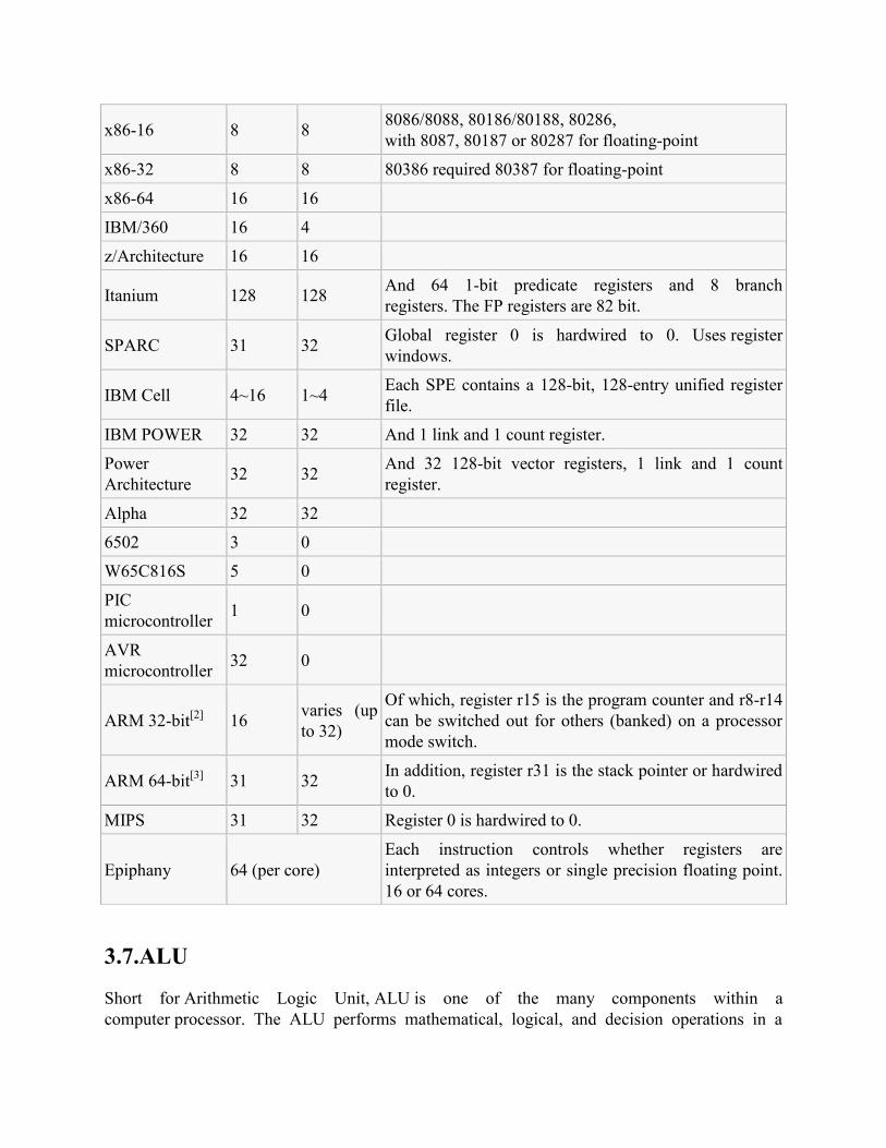
3.7.ALU
Short for Arithmetic Logic Unit, ALU is one of the many components within a computer processor. The ALU performs mathematical, logical, and decision operations in a
x86-16 8 8 8086/8088, 80186/80188, 80286, with 8087, 80187 or 80287 for floating-point
x86-32 8 8 80386 required 80387 for floating-point
x86-64 16 16 IBM/360 16 4 z/Architecture 16 16
Itanium 128 128 And 64 1-bit predicate registers and 8 branch registers. The FP registers are 82 bit.
SPARC 31 32 Global register 0 is hardwired to 0. Uses register windows.
IBM Cell 4~16 1~4 Each SPE contains a 128-bit, 128-entry unified register file.
IBM POWER 32 32 And 1 link and 1 count register.
Power Architecture
32 32 And 32 128-bit vector registers, 1 link and 1 count register.
Alpha 32 32 6502 3 0 W65C816S 5 0 PIC microcontroller
1 0
AVR microcontroller
32 0
ARM 32-bit[2] 16 varies (up to 32)
Of which, register r15 is the program counter and r8-r14 can be switched out for others (banked) on a processor mode switch.
ARM 64-bit[3] 31 32 In addition, register r31 is the stack pointer or hardwired to 0.
MIPS 31 32 Register 0 is hardwired to 0.
Epiphany 64 (per core) Each instruction controls whether registers are interpreted as integers or single precision floating point. 16 or 64 cores.
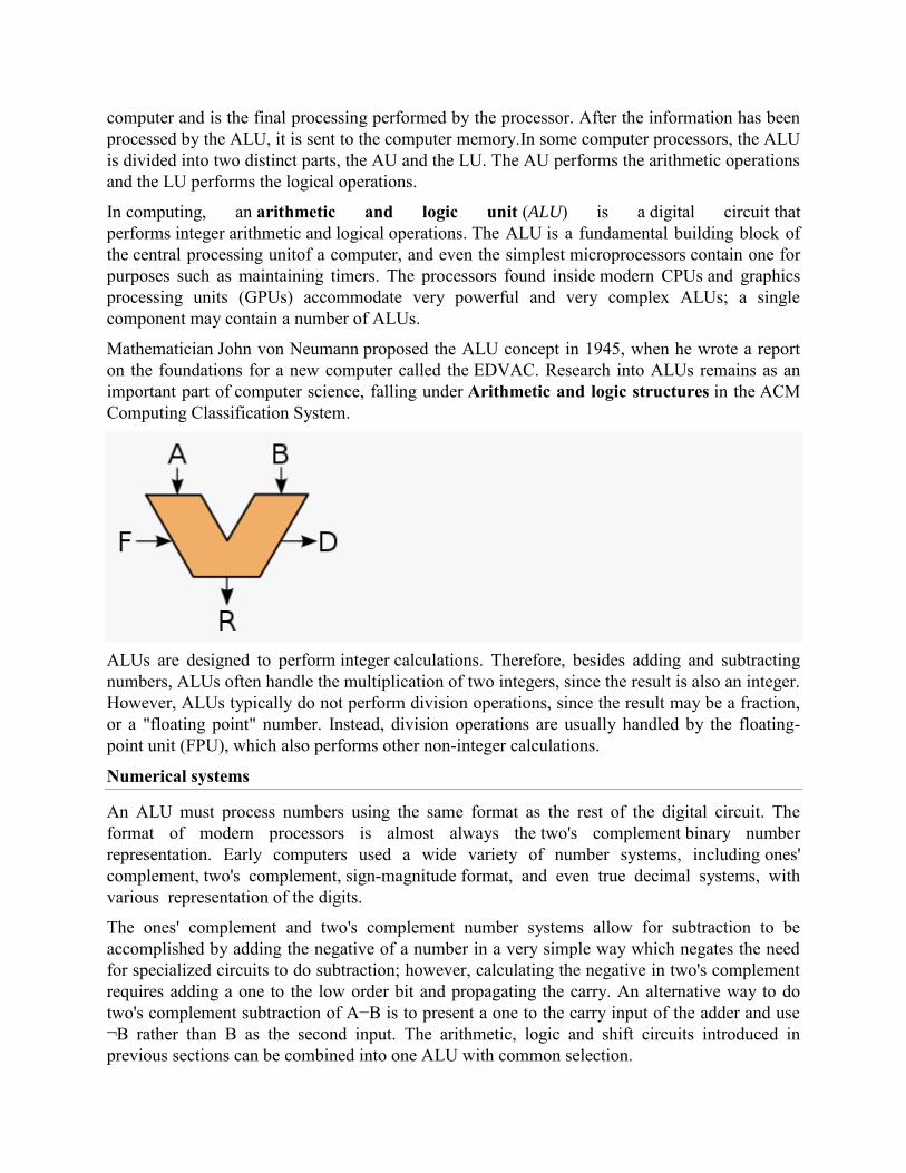
computer and is the final processing performed by the processor. After the information has been processed by the ALU, it is sent to the computer memory.In some computer processors, the ALU is divided into two distinct parts, the AU and the LU. The AU performs the arithmetic operations and the LU performs the logical operations.
In computing, an arithmetic and logic unit (ALU) is a digital circuit that performs integer arithmetic and logical operations. The ALU is a fundamental building block of the central processing unitof a computer, and even the simplest microprocessors contain one for purposes such as maintaining timers. The processors found inside modern CPUs and graphics processing units (GPUs) accommodate very powerful and very complex ALUs; a single component may contain a number of ALUs.
Mathematician John von Neumann proposed the ALU concept in 1945, when he wrote a report on the foundations for a new computer called the EDVAC. Research into ALUs remains as an important part of computer science, falling under Arithmetic and logic structures in the ACM Computing Classification System.
ALUs are designed to perform integer calculations. Therefore, besides adding and subtracting numbers, ALUs often handle the multiplication of two integers, since the result is also an integer. However, ALUs typically do not perform division operations, since the result may be a fraction, or a "floating point" number. Instead, division operations are usually handled by the floating-point unit (FPU), which also performs other non-integer calculations.
Numerical systems
An ALU must process numbers using the same format as the rest of the digital circuit. The format of modern processors is almost always the two's complement binary number representation. Early computers used a wide variety of number systems, including ones' complement, two's complement, sign-magnitude format, and even true decimal systems, with various representation of the digits.
The ones' complement and two's complement number systems allow for subtraction to be accomplished by adding the negative of a number in a very simple way which negates the need for specialized circuits to do subtraction; however, calculating the negative in two's complement requires adding a one to the low order bit and propagating the carry. An alternative way to do two's complement subtraction of A−B is to present a one to the carry input of the adder and use
¬B rather than B as the second input. The arithmetic, logic and shift circuits introduced in previous sections can be combined into one ALU with common selection.
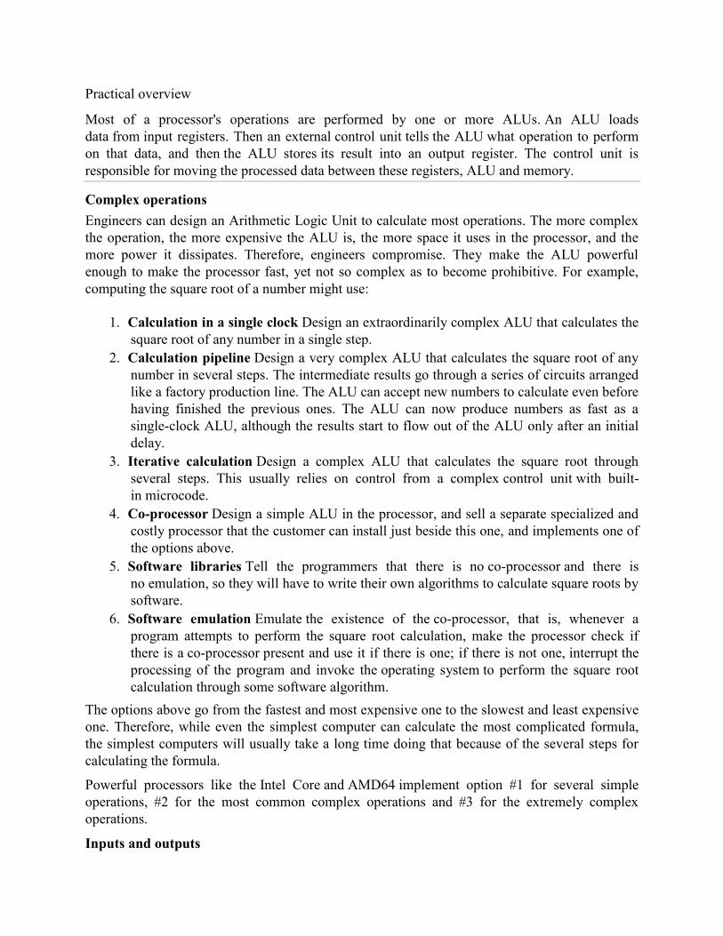
Practical overview
Most of a processor's operations are performed by one or more ALUs. An ALU loads data from input registers. Then an external control unit tells the ALU what operation to perform on that data, and then the ALU stores its result into an output register. The control unit is responsible for moving the processed data between these registers, ALU and memory.
Complex operations Engineers can design an Arithmetic Logic Unit to calculate most operations. The more complex the operation, the more expensive the ALU is, the more space it uses in the processor, and the more power it dissipates. Therefore, engineers compromise. They make the ALU powerful enough to make the processor fast, yet not so complex as to become prohibitive. For example, computing the square root of a number might use:
1. Calculation in a single clock Design an extraordinarily complex ALU that calculates the square root of any number in a single step.
2. Calculation pipeline Design a very complex ALU that calculates the square root of any number in several steps. The intermediate results go through a series of circuits arranged like a factory production line. The ALU can accept new numbers to calculate even before having finished the previous ones. The ALU can now produce numbers as fast as a single-clock ALU, although the results start to flow out of the ALU only after an initial delay.
3. Iterative calculation Design a complex ALU that calculates the square root through several steps. This usually relies on control from a complex control unit with built-in microcode.
4. Co-processor Design a simple ALU in the processor, and sell a separate specialized and costly processor that the customer can install just beside this one, and implements one of the options above.
5. Software libraries Tell the programmers that there is no co-processor and there is no emulation, so they will have to write their own algorithms to calculate square roots by software.
6. Software emulation Emulate the existence of the co-processor, that is, whenever a program attempts to perform the square root calculation, make the processor check if there is a co-processor present and use it if there is one; if there is not one, interrupt the processing of the program and invoke the operating system to perform the square root calculation through some software algorithm.
The options above go from the fastest and most expensive one to the slowest and least expensive one. Therefore, while even the simplest computer can calculate the most complicated formula, the simplest computers will usually take a long time doing that because of the several steps for calculating the formula.
Powerful processors like the Intel Core and AMD64 implement option #1 for several simple operations, #2 for the most common complex operations and #3 for the extremely complex operations.
Inputs and outputs
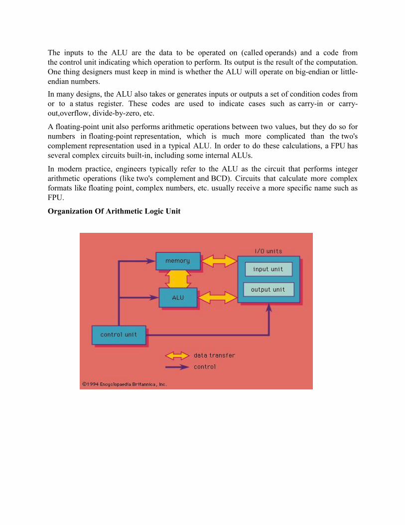
The inputs to the ALU are the data to be operated on (called operands) and a code from the control unit indicating which operation to perform. Its output is the result of the computation. One thing designers must keep in mind is whether the ALU will operate on big-endian or little-endian numbers. In many designs, the ALU also takes or generates inputs or outputs a set of condition codes from or to a status register. These codes are used to indicate cases such as carry-in or carry-out,overflow, divide-by-zero, etc.
A floating-point unit also performs arithmetic operations between two values, but they do so for numbers in floating-point representation, which is much more complicated than the two's complement representation used in a typical ALU. In order to do these calculations, a FPU has several complex circuits built-in, including some internal ALUs.
In modern practice, engineers typically refer to the ALU as the circuit that performs integer arithmetic operations (like two's complement and BCD). Circuits that calculate more complex formats like floating point, complex numbers, etc. usually receive a more specific name such as FPU.
Organization Of Arithmetic Logic Unit
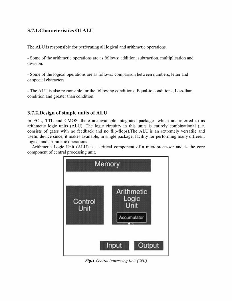
3.7.1.Characteristics Of ALU The ALU is responsible for performing all logical and arithmetic operations. - Some of the arithmetic operations are as follows: addition, subtraction, multiplication and division. - Some of the logical operations are as follows: comparison between numbers, letter and or special characters. - The ALU is also responsible for the following conditions: Equal-to conditions, Less-than condition and greater than condition.
3.7.2.Design of simple units of ALU In ECL, TTL and CMOS, there are available integrated packages which are referred to as arithmetic logic units (ALU). The logic circuitry in this units is entirely combinational (i.e. consists of gates with no feedback and no flip-flops).The ALU is an extremely versatile and useful device since, it makes available, in single package, facility for performing many different logical and arithmetic operations. Arithmetic Logic Unit (ALU) is a critical component of a microprocessor and is the core component of central processing unit.
Fig.1 Central Processing Unit (CPU)
ALU‘s comprise the combinational logic that implements logic operations such as AND, OR
and arithmetic operations, such as ADD, SUBTRACT. Functionally, the operation of typical ALU is represented as shown in diagram below,
Fig.2 Functional representation of Arithmetic Logic Unit
3.8.Control Unit The control unit maintains order within thecomputer system and directs the flow of traffic(operations) and data. The flow of control is indicatedby the dotted arrows on figure 1-1. The control unitselects one program statement at a time from theprogram storage area, interprets the statement, andsends the appropriate electronic impulses to thearithmetic-logic unit and storage section to cause themto carry out the instruction.The control unit does not perform the actualprocessing operations on the data. Specifically, thecontrol unit manages the operations of the CPU, be it asingle-chip microprocessor or a fill-size mainframe.Like a traffic director, it decides when to start and
stop(control and timing), what to do (program instructions),where to keep information (memory), and with whatdevices to communicate (I/O). It controls the flow of alldata entering and leaving the computer. It accomplishesthis by communicating or interfacing with thearithmetic-logic unit, memory, and I/O areas. Itprovides the computer with the ability to function underprogram control.Depending on the design of thecomputer, the CPU can also have the capability tofunction under manual control through man/machineinterfacing.The control unit consists of several basic logicallydefined areas.These logically defined areas workclosely with each other. Timing in a computer regulatesthe flow of signals that control the operation of thecomputer. The instruction and control portion makesup the decision-making and memory-type functions.Addressing is the process of locating the operand(specific information) for a given operation. Aninterrupt is a break in the normal flow of operation of acomputer (e.g., CTRL + ALT + DEL). Controlmemory is a random-access memory (RAM)consisting of addressable storage registers.Cachememory is a small, high-speed RAM buffer locatedbetween the CPU and main memory; it can increase thespeed of the PC. Read-only memory (ROM) are chipswith a set of software instructions supplied by themanufacturer built into them that enables the computerto perform its I/O operation.
The control unit is also capable of shutting down thecomputer when the power supply detects abnormalconditions
3.9.Hardwired Control Hardwired control units are implemented through use of sequential logic units, featuring a finite number of gates that can generate specific results based on the instructions that were used to invoke those responses. Hardwired control units are generally faster than microprogrammed designs.
Their design uses a fixed architecture — it requires changes in the wiring if the instruction set is modified or changed. This architecture is preferred in reduced instruction set computers (RISC) as they use a simpler instruction set.
A controller that uses this approach can operate at high speed. However, it has little flexibility, and the complexity of the instruction set it can implement is limited.
The hardwired approach has become less popular as computers have evolved as at one time, control units for CPUs were ad-hoc logic, and they were difficult to design.
3.10.Wilkes control Basically its function is to initiate the sequece of micro-operations to be performeed on the data stored in registers in computer.
Maurice Wilkes invented "microprogram" in 1953. He realised an idea that made a control unit easier to design and is more flexible. His idea is that a control unit can be implemented as a memory which contains patterns of the control bits and part of the flow control for sequencing
those patterns. Microprogram control unit is actually like a miniature computer which can be "programmed" to sequence the patterns of control bits. Its "program" is called "microprogram" to distinguish it from an ordinary computer program. Using microprogram, a control unit can be implemented for a complex instruction set which is impossible to do by hardwired. Wilkes told his realisation by his own words:
Maurice Wilkes 1953, he thought of a centralized control using diode matrix and, after visiting the Whirlwind computer in U.S., wrote :
I found that it did indeed have a centralized control based on the use of a matrix of diodes. It was, however, only capable of producing a fixed sequence of 8 pulses -- a different sequence for each instruction, but nevertheless fixed as far as a particular instruction was concerned. It was not, I think, until I got back to Cambridge that I realized that the solution was to turn the control unit into a computer in miniature by adding a second matrix to determine the flow of control at the microlevel and by providing for conditional micro-instructions. [Wilkes 1985] His idea was too far ahead of its time as it required high speed memory which was not possible at that time. Microprogram approach for control unit has several advantages : 1. One computer model can be microprogrammed to "emulate" other model. 2. One instruction set can be used throughout different models of hardware. 3. One hardware can realised many instruction sets. Therefore it is possible to choose the set that is most suitable for an application.
3.11.Micro-programmed control The idea of microprogramming was introduced by Maurice Wilkes in 1951 as an intermediate level to execute computer program instructions. Microprograms were organized as a sequence ofmicroinstructions and stored in special control memory. The algorithm for the microprogram control unit is usually specified by flowchart description.[1] The main advantage of the microprogram control unit is the simplicity of its structure. Outputs of the controller are organized in microinstructions and they can be easily replaced.
In hardwired control , we saw how all the control signals required inside the CPU can be generated
using a state counter and a PLA circuit.
There is an alternative approach by which the control signals required inside the CPU can be generated This alternative approach is known as microprogrammed control unit.
In microprogrammed control unit , the logic of the control unit is specified by a microprogram.Amicroprogram consists of a sequence of instructions in a microprogramming language. These are very instructions that specify microoperations.
A microprogrammed control unit is a relatively simple logic circuit that is capable of (1) sequencing through microinstructions and (2) generating control signals to execute each microinstruction.
The concept of microprogram is similar to computer program. In computer program the complete instructions of the program is stored in main memory and during execution it fetches the instructions from main memory one after another. The sequence of instruction fetch is controlled by program counter (PC) .
Microprogram are stored in microprogram memory and the execution is controlled by microprogram counter ( PC ) .Microprogram consists of microinstructions which are nothing but the strings of 0‘s and 1‘s . In a particular instance ,we read the contents of one location of microprogram memory , which is nothing but a microinstruction . Each output line ( data line ) of microprogram memory corresponds to one control signal. If the contents of the memory cell is ) , it indicates that the signal is to generated and if the contents of memory cell is 1 , it indicates that generate that control signal at that instant of time.
3.12.Microinstructions A single instruction in microcode. It is the most elementary instruction in the computer, such as moving the contents of a register to the arithmetic logic unit (ALU). It takes several microinstructions to carry out one complex machine instruction (CISC). Also called a "micro-op" or "µop," microinstructions differ within the same computer family and even the same vendor. For example, although all are x86 chips, the microcode for Intel's Pentium 4, Pentium M and AMD's Athlon are not the same. The software programmer never sees microinstructions, and they are not documented for the public
microinstruction: An instruction that controls data flow and instruction-execution sequencing in a processor at a more fundamental level than machine instructions. Note: A series of microinstructions is necessary to perform an individual machine instruction. a micro instruction specifies one or more micro oprations for the system.
Execution Of Micro-Program
The level of abstraction of a microprogram can vary according to the amount of control signal encoding and the amount of explicit parallelism found in the microinstruction format. On one end of a spectrum, a vertical microinstruction is highly encoded and may look like a simple macroinstruction containing a single opcode field and one or two operand specifiers. For example, see Figure 10, which shows an example of vertical microcode for a Microdata machine [Microdata].
; multiply two numbers LF 5,X'08' ; set loop counter to 8 MT 2 ; move X to T LF 4,X'00' ; clear ZU ADD: TZ 3,X'01' ; if Y bit 0 set to 1 A 4,T ; add X to Z H 4,R ; shift Z upper
H 3,L,R ; shift Z lower D 5,C ; decrement loop counter TN 0,X'04' ; if loop counter equal 0 JP ADD ; jump to top of loop
Each vertical microinstruction specifies a single datapath operation and, when decoded, activates multiple control signals. Branches within vertical microprograms are typically handled as separate microinstructions using a "branch" or "jump" opcode. This style of microprogramming is the most natural to someone experienced in regular assembly language programming, and is similar to programming in a RISC instruction set.
Horizontal microprogramming is therefore less familiar to traditional programmers and can be more error-prone. However, horizontal microprogramming typically provides better performance because of the opportunities to exploit parallelism within the datapath and to fold the microprogram branching decisions into the same clock cycle in which the datapath actions are being performed. Programming for horizontal microcode engines has been compared to the programming required for VLIW processors.
A combination of vertical and horizontal microinstructions in a two-level scheme is called nanoprogramming and was used in the Nanodata QM-1 and the Motorola 68000. The QM-1 used a 16K word microinstruction control store of 18 bits per word and a 1K word nanoinstruction control store of 360 bits per word [Nanodata]. The microinstructions essentially formed calls to routines at the nanoinstruction level. The horizontal-style nanoinstruction was divided into five 72-bit fields (see Figure 11).
SRDAI: "SHIFT RIGHT DOUBLE ARITHMETIC IMMEDIATE" .... FETCH, KSHC=RIGHT+DOUBLE+ARITHMETIC+RIGHT CTL, SH STATUS ENABLE KALC=PASS LEFT, ALU STATUS ENABLE S... A->FAIL, A->FSID, B->KSHR, CLEAR CIN .S.. A->FAOD, INCF->FSID, A->FSOD ..S. INCF->FSOD ...X GATE ALU, GATE SH, ALU TO COM
Review Questions
1. Explain central processing unit ? 2. What is instruction and instruction set? 3. What is instruction set architecture? 4. What is addressing mode and also explain the types of it? 5. What is register ? 6. What are the types of registers? 7. Explain the concept of microoperation? 8. Explain arithmetic logic unit with diagram? 9. What is characteristic of ALU? 10. What is micro-program control unit? 11. Describe control unit explain?
4.1.Assembly Language Programming
An assembly language is a low-level programming language for a computer, or other programmable device, in which there is a very strong (generallyone-to-one) correspondence between the language and the architecture's machine code instructions. Each assembly language is specific to a particularcomputer architecture, in contrast to most high-level programming languages, which are generally portable across multiple architectures, but requireinterpreters or compiling.
Assembly language is converted into executable machine code by a utility program referred to as an assembler; the conversion process is referred to as assembly, or assembling the code.
Assembly language uses a mnemonic to represent each low-level machine operation or opcode. Some opcodes require one or more operands as part of the instruction, and most assemblers can take labels and symbols as operands to represent addresses and constants, instead of hard coding them into the program. Macro assemblers include a macroinstruction facility so that assembly language text can be pre-assigned to a name, and that name can be used to insert the text into other code. Many assemblers offer additional mechanisms to facilitate program development, to control the assembly process, and to aid debugging.
A program written in assembly language consists of a series of (mnemonic) processor instructions and meta-statements (known variously as directives, pseudo-instructions and pseudo-ops), comments and data. Assembly language instructions usually consist of an opcode mnemonic followed by a list of data, arguments or parameters.[4] These are translated by an assembler intomachine language instructions that can be loaded into memory and executed.
For example, the instruction below tells an x86/IA-32 processor to move an immediate 8-bit value into a register. The binary code for this instruction is 10110 followed by a 3-bit identifier for which register to use. The identifier for the AL register is 000, so the following machine code loads the AL register with the data 01100001.
10110000 01100001
This binary computer code can be made more human-readable by expressing it in hexadecimal as follows
B0 61
Here, B0 means 'Move a copy of the following value into AL', and 61 is a hexadecimal representation of the value 01100001, which is 97 in decimal. Intel assembly language provides themnemonic MOV (an abbreviation of move) for instructions such as this, so the machine code
above can be written as follows in assembly language, complete with an explanatory comment if required, after the semicolon. This is much easier to read and to remember.
MOV AL, 61h ; Load AL with 97 decimal (61 hex) In some assembly languages the same mnemonic such as MOV may be used for a family of related instructions for loading, copying and moving data, whether these are immediate values, values in registers, or memory locations pointed to by values in registers. Other assemblers may use separate opcodes such as L for "move memory to register", ST for "move register to memory", LR for "move register to register", MVI for "move immediate operand to memory", etc.
The Intel opcode 10110000 (B0) copies an 8-bit value into the AL register, while 10110001 (B1) moves it into CL and 10110010 (B2) does so into DL. Assembly language examples for these follow.[5]
MOV AL, 1h ; Load AL with immediate value 1 MOV CL, 2h ; Load CL with immediate value 2 MOV DL, 3h ; Load DL with immediate value 3 The syntax of MOV can also be more complex as the following examples show.[6]
MOV EAX, [EBX] ; Move the 4 bytes in memory at the address contained in EBX into EAX MOV [ESI+EAX], CL ; Move the contents of CL into the byte at address ESI+EAX In each case, the MOV mnemonic is translated directly into an opcode in the ranges 88-8E, A0-A3, B0-B8, C6 or C7 by an assembler, and the programmer does not have to know or remember which.
Transforming assembly language into machine code is the job of an assembler, and the reverse can at least partially be achieved by a disassembler. Unlike high-level languages, there is usually aone-to-one correspondence between simple assembly statements and machine language instructions. However, in some cases, an assembler may provide pseudoinstructions (essentially macros) which expand into several machine language instructions to provide commonly needed functionality. For example, for a machine that lacks a "branch if greater or equal" instruction, an assembler may provide a pseudoinstruction that expands to the machine's "set if less than" and "branch if zero (on the result of the set instruction)". Most full-featured assemblers also provide a rich macro language (discussed below) which is used by vendors and programmers to generate more complex code and data sequences.
Each computer architecture has its own machine language. Computers differ in the number and type of operations they support, in the different sizes and numbers of registers, and in the representations of data in storage. While most general-purpose computers are able to carry out essentially the same functionality, the ways they do so differ; the corresponding assembly languages reflect these differences.
Multiple sets of mnemonics or assembly-language syntax may exist for a single instruction set, typically instantiated in different assembler programs. In these cases, the most popular one is usually that supplied by the manufacturer and used in its documentation.
Language design Basic elements
There is a large degree of diversity in the way the authors of assemblers categorize statements and in the nomenclature that they use. In particular, some describe anything other than a machine mnemonic or extended mnemonic as a pseudo-operation (pseudo-op). A typical assembly language consists of 3 types of instruction statements that are used to define program operations:
Opcode mnemonics Data sections Assembly directives
Opcode mnemonics and extended mnemonics Instructions (statements) in assembly language are generally very simple, unlike those in high-level language. Generally, a mnemonic is a symbolic name for a single executable machine language instruction (an opcode), and there is at least one opcode mnemonic defined for each machine language instruction. Each instruction typically consists of an operation or opcode plus zero or more operands. Most instructions refer to a single value, or a pair of values. Operands can be immediate (value coded in the instruction itself), registers specified in the instruction or implied, or the addresses of data located elsewhere in storage. This is determined by the underlying processor architecture: the assembler merely reflects how this architecture works. Extended mnemonics are often used to specify a combination of an opcode with a specific operand, e.g., the System/360 assemblers use B as an extended mnemonic for BC with a mask of 15 and NOP("NO OPeration" - do nothing for one step) for BC with a mask of 0. Extended mnemonics are often used to support specialized uses of instructions, often for purposes not obvious from the instruction name. For example, many CPU's do not have an explicit NOP instruction, but do have instructions that can be used for the purpose. In 8086 CPUs the instruction xchg ax,ax is used for nop, with nop being a pseudo-opcode to encode the instruction xchg ax,ax. Some disassemblers recognize this and will decode the xchg ax,ax instruction as nop. Similarly, IBM assemblers for System/360 and System/370 use the extended mnemonics NOP andNOPR for BC and BCR with zero masks. For the SPARC architecture, these are known as synthetic instructions
Some assemblers also support simple built-in macro-instructions that generate two or more machine instructions. For instance, with some Z80 assemblers the instruction ld hl,bc is recognized to generate ld l,c followed by ld h,b. These are sometimes known as pseudo-opcodes.
Mnemonics are arbitrary symbols; in 1985 the IEEE published Standard 694 for a uniform set of mnemonics to be used by all assemblers. The standard has since been withdrawn.
Data directives There are instructions used to define data elements to hold data and variables. They define the type of data, the length and the alignment of data. These instructions can also define whether the
data is available to outside programs (programs assembled separately) or only to the program in which the data section is defined. Some assemblers classify these as pseudo-ops. Assembly directives Assembly directives, also called pseudo opcodes, pseudo-operations or pseudo-ops, are instructions that are executed by an assembler at assembly time, not by a CPU at run time. They can make the assembly of the program dependent on parameters input by a programmer, so that one program can be assembled different ways, perhaps for different applications. They also can be used to manipulate presentation of a program to make it easier to read and maintain. (For example, directives would be used to reserve storage areas and optionally their initial contents.) The names of directives often start with a dot to distinguish them from machine instructions.
Symbolic assemblers let programmers associate arbitrary names (labels or symbols) with memory locations. Usually, every constant and variable is given a name so instructions can reference those locations by name, thus promoting self-documenting code. In executable code, the name of each subroutine is associated with its entry point, so any calls to a subroutine can use its name. Inside subroutines, GOTO destinations are given labels. Some assemblers support local symbols which are lexically distinct from normal symbols (e.g., the use of "10$" as a GOTO destination).
Some assemblers, such as NASM provide flexible symbol management, letting programmers manage different namespaces, automatically calculate offsets within data structures, and assign labels that refer to literal values or the result of simple computations performed by the assembler. Labels can also be used to initialize constants and variables with relocatable addresses.
Assembly languages, like most other computer languages, allow comments to be added to assembly source code that are ignored by the assembler. Good use of comments is even more important with assembly code than with higher-level languages, as the meaning and purpose of a sequence of instructions is harder to decipher from the code itself.
Wise use of these facilities can greatly simplify the problems of coding and maintaining low-level code. Raw assembly source code as generated by compilers or disassemblers—code without any comments, meaningful symbols, or data definitions—is quite difficult to read when changes must be made.
Macros Many assemblers support predefined macros, and others support programmer-defined (and repeatedly re-definable) macros involving sequences of text lines in which variables and constants are embedded. This sequence of text lines may include opcodes or directives. Once a macro has been defined its name may be used in place of a mnemonic. When the assembler processes such a statement, it replaces the statement with the text lines associated with that macro, then processes them as if they existed in the source code file (including, in some assemblers, expansion of any macros existing in the replacement text).
Note that this definition of "macro" is slightly different from the use of the term in other contexts, like the C programming language. C macros created through the #define directive
typically are just one line, or a few lines at most. Assembler macro instructions can be lengthy "programs" by themselves, executed by interpretation by the assembler during assembly.
Since macros can have 'short' names but expand to several or indeed many lines of code, they can be used to make assembly language programs appear to be far shorter, requiring fewer lines of source code, as with higher level languages. They can also be used to add higher levels of structure to assembly programs, optionally introduce embedded debugging code via parameters and other similar features.
Macro assemblers often allow macros to take parameters. Some assemblers include quite sophisticated macro languages, incorporating such high-level language elements as optional parameters, symbolic variables, conditionals, string manipulation, and arithmetic operations, all usable during the execution of a given macro, and allowing macros to save context or exchange information. Thus a macro might generate a large number of assembly language instructions or data definitions, based on the macro arguments. This could be used to generate record-style data structures or "unrolled" loops, for example, or could generate entire algorithms based on complex parameters. An organization using assembly language that has been heavily extended using such a macro suite can be considered to be working in a higher-level language, since such programmers are not working with a computer's lowest-level conceptual elements.
Macros were used to customize large scale software systems for specific customers in the mainframe era and were also used by customer personnel to satisfy their employers' needs by making specific versions of manufacturer operating systems. This was done, for example, by systems programmers working with IBM's Conversational Monitor System / Virtual Machine (VM/CMS) and with IBM's "real time transaction processing" add-ons, Customer Information Control System CICS, and ACP/TPF, the airline/financial system that began in the 1970s and still runs many largecomputer reservations systems (CRS) and credit card systems today.
It was also possible to use solely the macro processing abilities of an assembler to generate code written in completely different languages, for example, to generate a version of a program inCOBOL using a pure macro assembler program containing lines of COBOL code inside assembly time operators instructing the assembler to generate arbitrary code.
This was because, as was realized in the 1960s, the concept of "macro processing" is independent of the concept of "assembly", the former being in modern terms more word processing, text processing, than generating object code. The concept of macro processing appeared, and appears, in the C programming language, which supports "preprocessor instructions" to set variables, and make conditional tests on their values. Note that unlike certain previous macro processors inside assemblers, the C preprocessor was not Turing-complete because it lacked the ability to either loop or "go to", the latter allowing programs to loop.
Despite the power of macro processing, it fell into disuse in many high level languages (major exceptions being C/C++ and PL/I) while remaining a perennial for assemblers.
Macro parameter substitution is strictly by name: at macro processing time, the value of a parameter is textually substituted for its name. The most famous class of bugs resulting was the use of a parameter that itself was an expression and not a simple name when the macro writer expected a name. In the macro: foo: macro a load a*b the intention was that the caller would provide the name of a variable, and the "global" variable or constant b would be used to multiply
"a". If foo is called with the parameter a-c, the macro expansion of load a-c*b occurs. To avoid any possible ambiguity, users of macro processors can parenthesize formal parameters inside macro definitions, or callers can parenthesize the input parameters
Support for structured programming Some assemblers have incorporated structured programming elements to encode execution flow. The earliest example of this approach was in the Concept-14 macro set, originally proposed by Dr. H.D. Mills (March, 1970), and implemented by Marvin Kessler at IBM's Federal Systems Division, which extended the S/360 macro assembler with IF/ELSE/ENDIF and similar control flow blocks.[10] This was a way to reduce or eliminate the use of GOTO operations in assembly code, one of the main factors causing spaghetti code in assembly language. This approach was widely accepted in the early '80s (the latter days of large-scale assembly language use). A curious design was A-natural, a "stream-oriented" assembler for 8080/Z80 processors[citation
needed] from Whitesmiths Ltd. (developers of the Unix-like Idris operating system, and what was reported to be the first commercial C compiler). The language was classified as an assembler, because it worked with raw machine elements such as opcodes, registers, and memory references; but it incorporated an expression syntax to indicate execution order. Parentheses and other special symbols, along with block-oriented structured programming constructs, controlled the sequence of the generated instructions. A-natural was built as the object language of a C compiler, rather than for hand-coding, but its logical syntax won some fans.
There has been little apparent demand for more sophisticated assemblers since the decline of large-scale assembly language development. In spite of that, they are still being developed and applied in cases where resource constraints or peculiarities in the target system's architecture prevent the effective use of higher-level languages.
4.2.Microprocessor
A microprocessor incorporates the functions of a computer's central processing unit (CPU) on a single integrated circuit (IC), or at most a few integrated circuits. It is a multipurpose, programmable device that accepts digital data as input, processes it according to instructions stored in its memory, and provides results as output. It is an example of sequential digital logic, as it has internal memory. Microprocessors operate on numbers and symbols represented in the binary numeral system.
The advent of low-cost computers on integrated circuits has transformed modern society. General-purpose microprocessors in personal computers are used for computation, text editing, multimedia display, and communication over the Internet. Many more microprocessors are part of embedded systems, providing digital control over myriad objects from appliances to automobiles to cellular phones and industrial process control.
Intel introduced its first 4-bit microprocessor 4004 in 1971 and its 8-bit microprocessor 8008 in 1972. During the 1960s, computer processors were constructed out of small and medium-scale ICs—each containing from tens to a few hundred transistors. These were placed and soldered onto printed circuit boards, and often multiple boards were interconnected in a chassis. The large number of discrete logic gates used more electrical power—and therefore produced more heat—
than a more integrated design with fewer ICs. The distance that signals had to travel between ICs on the boards limited a computer's operating speed.
In the NASA Apollo space missions to the moon in the 1960s and 1970s, all onboard computations for primary guidance, navigation and control were provided by a small custom processor called "The Apollo Guidance Computer". It used wire wrap circuit boards whose only logic elements were three-input NOR gates.
The integration of a whole CPU onto a single chip or on a few chips greatly reduced the cost of processing power. The integrated circuit processor was produced in large numbers by highly automated processes, so unit cost was low. Single-chip processors increase reliability as there are many fewer electrical connections to fail. As microprocessor designs get faster, the cost of manufacturing a chip (with smaller components built on a semiconductor chip the same size) generally stays the same.
Microprocessors integrated into one or a few large-scale ICs the architectures that had previously been implemented using many medium- and small-scale integrated circuits. Continued increases in microprocessor capacity have rendered other forms of computers almost completely obsolete (see history of computing hardware), with one or more microprocessors used in everything from the smallest embedded systems and handheld devices to the largest mainframes and supercomputers.
The first microprocessors emerged in the early 1970s and were used for electronic calculators, using binary-coded decimal (BCD) arithmetic on 4-bit words. Other embedded uses of 4-bit and 8-bit microprocessors, such as terminals, printers, various kinds of automation etc., followed soon after. Affordable 8-bit microprocessors with 16-bit addressing also led to the first general-purposemicrocomputers from the mid-1970s on.
Since the early 1970s, the increase in capacity of microprocessors has followed Moore's law; this originally suggested that the number of components that can be fitted onto a chip doubles every year. With present technology, it is actually every two years,[4] and as such Moore later changed the period to two years
Embedded applications
Thousands of items that were traditionally not computer-related include microprocessors. These include large and small household appliances, cars (and their accessory equipment units), car keys, tools and test instruments, toys, light switches/dimmers and electrical circuit breakers, smoke alarms, battery packs, and hi-fi audio/visual components (from DVD players to phonograph turntables). Such products as cellular telephones, DVD video system and HDTV broadcast systems fundamentally require consumer devices with powerful, low-cost, microprocessors. Increasingly stringent pollution control standards effectively require automobile manufacturers to use microprocessor engine management systems, to allow optimal control of emissions over widely varying operating conditions of an automobile. Non-programmable controls would require complex, bulky, or costly implementation to achieve the results possible with a microprocessor
A microprocessor control program (embedded software) can be easily tailored to different needs of a product line, allowing upgrades in performance with minimal redesign of the product. Different features can be implemented in different models of a product line at negligible production cost.
Microprocessor control of a system can provide control strategies that would be impractical to implement using electromechanical controls or purpose-built electronic controls. For example, an engine control system in an automobile can adjust ignition timing based on engine speed, load on the engine, ambient temperature, and any observed tendency for knocking—allowing an automobile to operate on a range of fuel grades.
Structure
The internal arrangement of a microprocessor varies depending on the age of the design and the intended purposes of the processor. The complexity of an integrated circuit is bounded by physical limitations of the number of transistors that can be put onto one chip, the number of package terminations that can connect the processor to other parts of the system, the number of interconnections it is possible to make on the chip, and the heat that the chip can dissipate. Advancing technology makes more complex and powerful chips feasible to manufacture.
A minimal hypothetical microprocessor might only include an arithmetic logic unit (ALU) and a control logic section. The ALU performs operations such as addition, subtraction, and operations such as AND or OR. Each operation of the ALU sets one or more flags in a status register, which indicate the results of the last operation (zero value, negative number, overflow. or others). The logic section retrieves instruction operation codes from memory, and initiates whatever sequence of operations of the ALU requires to carry out the instruction. A single operation code might affect many individual data paths, registers, and other elements of the processor.
As integrated circuit technology advanced, it was feasible to manufacture more and more complex processors on a single chip. The size of data objects became larger; allowing more transistors on a chip allowed word sizes to increase from 4- and 8-bit words up to today's 64-bit words. Additional features were added to the processor architecture; more on-chip registers sped up programs, and complex instructions could be used to make more compact programs. Floating-point arithmetic, for example, was often not available on 8-bit microprocessors, but had to be carried out in software. Integration of the floating point unit first as a separate integrated circuit and then as part of the same microprocessor chip, sped up floating point calculations.
Occasionally, physical limitations of integrated circuits made such practices as a bit slice approach necessary. Instead of processing all of a long word on one integrated circuit, multiple circuits in parallel processed subsets of each data word. While this required extra logic to handle, for example, carry and overflow within each slice, the result was a system that could handle, say, 32-bit words using integrated circuits with a capacity for only 4 bits each.
With the ability to put large numbers of transistors on one chip, it becomes feasible to integrate memory on the same die as the processor. This CPU cache has the advantage of faster access than off-chip memory, and increases the processing speed of the system for many applications. Generally, processor speed has increased more rapidly than external memory speed, so cache memory is necessary if the processor is not delayed by slower external memory.
Firsts
Three projects delivered a microprocessor at about the same time: Garrett AiResearch's Central Air Data Computer (CADC) (1968), Texas Instruments (TI) TMS 1000 (1971 September), and Intel's4004 (1971 November).
CADC In 1968, Garrett AiResearch (which employed designers Ray Holt and Steve Geller) was invited to produce a digital computer to compete with electromechanical systems then under development for the main flight control computer in the US Navy's new F-14 Tomcat fighter. The design was complete by 1970, and used a MOS-based chipset as the core CPU. The design was significantly (approximately 20 times) smaller and much more reliable than the mechanical systems it competed against, and was used in all of the early Tomcat models. This system contained "a 20-bit, pipelined, parallel multi-microprocessor". The Navy refused to allow publication of the design until 1997. For this reason the CADC, and the MP944 chipset it used, are fairly unknown. Ray Holtgraduated California Polytechnic University in 1968, and began his computer design career with the CADC. From its inception, it was shrouded in secrecy until 1998 when at Holt's request, the US Navy allowed the documents into the public domain. Since then several have debated if this was the first microprocessor. Holt has stated that no one has compared this microprocessor with those that came later. According to Parab et al. (2007), "The scientific papers and literature published around 1971 reveal that the MP944 digital processor used for the F-14 Tomcataircraft of the US Navy qualifies as the first microprocessor. Although interesting, it was not a single-chip processor, as was not the Intel 4004 – they both were more like a set of parallel building blocks you could use to make a general-purpose form. It contains a CPU, RAM, ROM, and two other support chips like the Intel 4004. Interesting it was made from the exact P-Channel technology and operated at Mil Spec's with larger chips. An excellent computer engineering design by any standards. Its design indicates a major advance over Intel and two year earlier. It actually worked and was flying in the F-14 when the Intel 4004 was announced. It indicates that today‘s industry theme of converging DSP-microcontroller architectures was started in 1971. This convergence of DSP and microcontroller architectures is known as a Digital Signal Controller Gilbert Hyatt Gilbert Hyatt was awarded a patent claiming an invention pre-dating both TI and Intel, describing a "microcontroller". The patent was later invalidated, but not before substantial royalties were paid out.
TMS 1000
The Smithsonian Institution says TI engineers Gary Boone and Michael Cochran succeeded in creating the first microcontroller (also called a microcomputer) and the first lone-chipped CPU in 1971. The result of their work was the TMS 1000, which went commercial in 1974.] TI stressed the 4-bit TMS 1000 for use in pre-programmed embedded applications, introducing a version called the TMS1802NC on September 17, 1971 that implemented a calculator on a chip.
TI filed for a patent on the microprocessor. Gary Boone was awarded U.S. Patent 3,757,306 for the single-chip microprocessor architecture on September 4, 1973. In 1971 and again in 1976, Intel and TI entered into broad patent cross-licensing agreements, with Intel paying royalties to TI for the microprocessor patent. A history of these events is contained in court documentation from a legal dispute between Cyrix and Intel, with TI as intervenor and owner of the microprocessor patent.
A computer-on-a-chip combines the microprocessor core (CPU), memory, and I/O (input/output) lines onto one chip. The computer-on-a-chip patent, called the "microcomputer patent" at the time,U.S. Patent 4,074,351, was awarded to Gary Boone and Michael J. Cochran of TI. Aside from this patent, the standard meaning of microcomputer is a computer using one or more microprocessors as its CPU(s), while the concept defined in the patent is more akin to a microcontroller.
Intel 4004 The Intel 4004 is generally regarded as the first commercially available microprocessor,and cost $60.[15] The first known advertisement for the 4004 is dated November 15, 1971 and appeared in Electronic News.The project that produced the 4004 originated in 1969, when Busicom, a Japanese calculator manufacturer, asked Intel to build a chipset for high-performance desktop calculators. Busicom's original design called for a programmable chip set consisting of seven different chips. Three of the chips were to make a special-purpose CPU with its program stored in ROM and its data stored in shift register read-write memory. Ted Hoff, the Intel engineer assigned to evaluate the project, believed the Busicom design could be simplified by using dynamic RAM storage for data, rather than shift register memory, and a more traditional general-purpose CPU architecture. Hoff came up with a four–chip architectural proposal: a ROM chip for storing the programs, a dynamic RAM chip for storing data, a simple I/O device and a 4-bit central processing unit (CPU). Although not a chip designer, he felt the CPU could be integrated into a single chip, but as he lacked the technical know-how the idea remained just a wish for the time being.
While the architecture and specifications of the MCS-4 came from the interaction of Hoff with Stanley Mazor, a software engineer reporting to him, and with Busicom engineer Masatoshi Shima, during 1969, Mazor and Hoff moved on to other projects. In April 1970, Intel hired Italian-born engineer Federico Faggin as project leader, a move that ultimately made the single-chip CPU final design a reality (Shima instead designed the Busicom calculator firmware and assisted Faggin during the first six months of the implementation). Faggin, who originally developed the silicon gatetechnology (SGT) in 1968 at Fairchild Semiconductor and designed the world‘s first commercial integrated circuit using SGT, the Fairchild 3708, had the correct
background to lead the project into what would become the first commercial general purpose microprocessor, since it was his very own invention, SGT in addition to his new methodology for random logic design, that made it possible to implement a single-chip CPU with the proper speed, power dissipation and cost. The manager of Intel's MOS Design Department was Leslie L. Vadász. at the time of the MCS-4 development, but Vadasz's attention was completely focused on the mainstream business of semiconductor memories and he left the leadership and the management of the MCS-4 project to Faggin, who was ultimately responsible for leading the
4004 project to its realization. Production units of the 4004 were first delivered to Busicom in March 1971 and shipped to other customers in late 1971.
Pico/General Instrument In 1971 Pico Electronics and General Instrument (GI) introduced their first collaboration in ICs, a complete single chip calculator IC for the Monroe/Litton Royal Digital III calculator. This chip could also arguably lay claim to be one of the first microprocessors or microcontrollers havingROM, RAM and a RISC instruction set on-chip. The layout for the four layers of the PMOS process was hand drawn at x500 scale on mylar film, a significant task at the time given the complexity of the chip. Pico was a spinout by five GI design engineers whose vision was to create single chip calculator ICs. They had significant previous design experience on multiple calculator chipsets with both GI and Marconi-Elliott The key team members had originally been tasked by Elliott Automation to create an 8 bit computer in MOS and had helped establish a MOS Research Laboratory in Glenrothes, Scotland in 1967.
Calculators were becoming the largest single market for semiconductors and Pico and GI went on to have significant success in this burgeoning market. GI continued to innovate in microprocessors and microcontrollers with products including the CP1600, IOB1680 and PIC1650. In 1987 the GI Microelectronics business was spun out into the Microchip PIC microcontroller business.
Four-Phase Systems AL1 The Four-Phase Systems AL1 was an 8-bit bit slice chip containing eight registers and an ALU. It was designed by Lee Boysel in 1969.At the time, it formed part of a nine-chip, 24-bit CPU with three AL1s, but it was later called a microprocessor when, in response to 1990s litigation by Texas Instruments, a demonstration system was constructed where a single AL1 formed part of a courtroom demonstration computer system, together with RAM, ROM, and an input-output device. 8-bit designs
The Intel 4004 was followed in 1972 by the Intel 8008, the world's first 8-bit microprocessor. The 8008 was not, however, an extension of the 4004 design, but instead the culmination of a separate design project at Intel, arising from a contract with Computer Terminals Corporation, of San Antonio TX, for a chip for a terminal they were designing, the Datapoint 2200 — fundamental aspects of the design came not from Intel but from CTC. In 1968, CTC's Vic Poor and Harry Pyle developed the original design for the instruction set and operation of the processor. In 1969, CTC contracted two companies, Intel and Texas Instruments, to make a single-chip implementation, known as the CTC 1201. In late 1970 or early 1971, TI dropped out being unable to make a reliable part. In 1970, with Intel yet to deliver the part, CTC opted to use their own implementation in the Datapoint 2200, using traditional TTL logic instead (thus the first machine to run ―8008 code‖ was not in fact a microprocessor at all and was delivered a year
earlier). Intel's version of the 1201 microprocessor arrived in late 1971, but was too late, slow, and required a number of additional support chips. CTC had no interest in using it. CTC had originally contracted Intel for the chip, and would have owed them $50,000 for their design
work. To avoid paying for a chip they did not want (and could not use), CTC released Intel from their contract and allowed them free use of the design. Intel marketed it as the 8008 in April, 1972, as the world's first 8-bit microprocessor. It was the basis for the famous "Mark-8" computer kit advertised in the magazine Radio-Electronics in 1974.
The 8008 was the precursor to the very successful Intel 8080 (1974), which offered much improved performance over the 8008 and required fewer support chips, Zilog Z80 (1976), and derivative Intel 8-bit processors. The competing Motorola 6800 was released August 1974 and the similar MOS Technology 6502 in 1975 (both designed largely by the same people). The 6502 family rivaled the Z80 in popularity during the 1980s.
A low overall cost, small packaging, simple computer bus requirements, and sometimes the integration of extra circuitry (e.g. the Z80's built-in memory refresh circuitry) allowed the home computer "revolution" to accelerate sharply in the early 1980s. This delivered such inexpensive machines as the Sinclair ZX-81, which sold for US$99. A variation of the 6502, the MOS Technology 6510 was used in the Commodore 64 and yet another variant, the 8502, powered the Commodore 128.
The Western Design Center, Inc (WDC) introduced the CMOS 65C02 in 1982 and licensed the design to several firms. It was used as the CPU in the Apple IIe and IIc personal computers as well as in medical implantable grade pacemakers and defibrillators, automotive, industrial and consumer devices. WDC pioneered the licensing of microprocessor designs, later followed by ARM and other microprocessor Intellectual Property (IP) providers in the 1990s.
Motorola introduced the MC6809 in 1978, an ambitious and thought-through 8-bit design source compatible with the 6800 and implemented using purely hard-wired logic. (Subsequent 16-bit microprocessors typically used microcode to some extent, as CISC design requirements were getting too complex for purely hard-wired logic only.)
Another early 8-bit microprocessor was the Signetics 2650, which enjoyed a brief surge of interest due to its innovative and powerful instruction set architecture.
A seminal microprocessor in the world of spaceflight was RCA's RCA 1802 (aka CDP1802, RCA COSMAC) (introduced in 1976), which was used on board the Galileo probe to Jupiter (launched 1989, arrived 1995). RCA COSMAC was the first to implement CMOS technology. The CDP1802 was used because it could be run at very low power, and because a variant was available fabricated using a special production process (Silicon on Sapphire), providing much better protection against cosmic radiation and electrostatic discharges than that of any other processor of the era. Thus, the SOS version of the 1802 was said to be the first radiation-hardened microprocessor.
The RCA 1802 had what is called a static design, meaning that the clock frequency could be made arbitrarily low, even to 0 Hz, a total stop condition. This let the Galileo spacecraft use minimum electric power for long uneventful stretches of a voyage. Timers or sensors would awaken the processor in time for important tasks, such as navigation updates, attitude control, data acquisition, and radio communication. Current versions of the Western Design Center 65C02 and 65C816 have static cores, and thus retain data even when the clock is completely halted.
12-bit designs
The Intersil 6100 family consisted of a 12-bit microprocessor (the 6100) and a range of peripheral support and memory ICs. The microprocessor recognised the DEC PDP-8 minicomputerinstruction set. As such it was sometimes referred to as the CMOS-PDP8. Since it was also produced by Harris Corporation, it was also known as the Harris HM-6100. By virtue of its CMOS technology and associated benefits, the 6100 was being incorporated into some military designs until the early 1980s.
16-bit designs
The first multi-chip 16-bit microprocessor was the National Semiconductor IMP-16, introduced in early 1973. An 8-bit version of the chipset was introduced in 1974 as the IMP-8.
Other early multi-chip 16-bit microprocessors include one that Digital Equipment Corporation (DEC) used in the LSI-11 OEM board set and the packaged PDP 11/03 minicomputer—and theFairchild Semiconductor MicroFlame 9440, both introduced in 1975-1976. In 1975, National introduced the first 16-bit single-chip microprocessor, the National Semiconductor PACE, which was later followed by an NMOS version, the INS8900.
Another early single-chip 16-bit microprocessor was TI's TMS 9900, which was also compatible with their TI-990 line of minicomputers. The 9900 was used in the TI 990/4 minicomputer, the TI-99/4A home computer, and the TM990 line of OEM microcomputer boards. The chip was packaged in a large ceramic 64-pin DIP package, while most 8-bit microprocessors such as the Intel 8080 used the more common, smaller, and less expensive plastic 40-pin DIP. A follow-on chip, the TMS 9980, was designed to compete with the Intel 8080, had the full TI 990 16-bit instruction set, used a plastic 40-pin package, moved data 8 bits at a time, but could only address 16 KB. A third chip, the TMS 9995, was a new design. The family later expanded to include the 99105 and 99110.
The Western Design Center (WDC) introduced the CMOS 65816 16-bit upgrade of the WDC CMOS 65C02 in 1984. The 65816 16-bit microprocessor was the core of the Apple IIgs and later theSuper Nintendo Entertainment System, making it one of the most popular 16-bit designs of all time.
Intel "upsized" their 8080 design into the 16-bit Intel 8086, the first member of the x86 family, which powers most modern PC type computers. Intel introduced the 8086 as a cost effective way of porting software from the 8080 lines, and succeeded in winning much business on that premise. The 8088, a version of the 8086 that used an 8-bit external data bus, was the microprocessor in the first IBM PC. Intel then released the 80186 and 80188, the 80286 and, in 1985, the 32-bit 80386, cementing their PC market dominance with the processor family's backwards compatibility. The 80186 and 80188 were essentially versions of the 8086 and 8088, enhanced with some onboard peripherals and a few new instructions; they were not used in IBM-compatible PCs because the built-in perpherals and their locations in the memory map were incompatible with the IBM design. The 8086 and successors had an innovative but limited method of memory segmentation, while the 80286 introduced a full-featured segmented memory management unit (MMU). The 80386 introduced a flat 32-bit memory model with paged memory management.
The Intel x86 processors up to and including the 80386 do not include floating-point units (FPUs). Intel introduced the 8087, 80287, and 80387 math coprocessors to add hardware floating-point and transcendental function capabilities to the 8086 through 80386 CPUs. The 8087 works with the 8086/8088 and 80186/80188, the 80187 works with the 80186/80188, the 80287 works with the 80286 and 80386, and the 80387 works with the 80386 (yielding better performance than the 80287). The combination of an x86 CPU and an x87 coprocessor forms a single multi-chip microprocessor; the two chips are programmed as a unit using a single integrated instruction set. Though the 8087 coprocessor is interfaced to the CPU through I/O ports in the CPU's address space, this is transparent to the program, which does not need to know about or access these I/O ports directly; the program accesses the coprocessor and its registers through normal instruction opcodes. Starting with the successor to the 80386, the 80486, the FPU was integrated with the control unit, MMU, and integer ALU in a pipelined design on a single chip (in the 80486DX version), or the FPU was eliminated entirely (in the 80486SX version). An ostensible coprocessor for the 80486SX, the 80487 was actually a complete 80486DX that disabled and replaced the coprocessorless 80486SX that it was installed to upgrade.
32-bit designs
16-bit designs had only been on the market briefly when 32-bit implementations started to appear.
The most significant of the 32-bit designs is the Motorola MC68000, introduced in 1979. The 68K, as it was widely known, had 32-bit registers in its programming model but used 16-bit internal data paths, 3 16-bit Arithmetic Logic Units, and a 16-bit external data bus (to reduce pin count), and externally supported only 24-bit addresses (internally it worked with full 32 bit addresses). In PC-based IBM-compatible mainframes the MC68000 internal microcode was modified to emulate the 32-bit System/370 IBM mainframe. Motorola generally described it as a 16-bit processor, though it clearly has 32-bit capable architecture. The combination of high performance, large (16 megabytes or 224 bytes) memory space and fairly low cost made it the most popular CPU design of its class. The Apple Lisa and Macintosh designs made use of the 68000, as did a host of other designs in the mid-1980s, including the Atari ST and Commodore Amiga.
The world's first single-chip fully 32-bit microprocessor, with 32-bit data paths, 32-bit buses, and 32-bit addresses, was the AT&T Bell Labs BELLMAC-32A, with first samples in 1980, and general production in 1982[32][33] After the divestiture of AT&T in 1984, it was renamed the WE 32000 (WE forWestern Electric), and had two follow-on generations, the WE 32100 and WE 32200. These microprocessors were used in the AT&T 3B5 and 3B15 minicomputers; in the 3B2, the world's first desktop supermicrocomputer; in the "Companion", the world's first 32-bit laptop computer; and in "Alexander", the world's first book-sized supermicrocomputer, featuring ROM-pack memory cartridges similar to today's gaming consoles. All these systems ran the UNIX System V operating system.
Intel's first 32-bit microprocessor was the iAPX 432, which was introduced in 1981 but was not a commercial success. It had an advanced capability-based object-oriented architecture, but poor performance compared to contemporary architectures such as Intel's own 80286 (introduced
1982), which was almost four times as fast on typical benchmark tests. However, the results for the iAPX432 was partly due to a rushed and therefore suboptimal Ada compiler. The ARM first appeared in 1985. This is a RISC processor design, which has since come to dominate the 32-bit embedded systems processor space due in large part to its power efficiency, its licensing model, and its wide selection of system development tools. Semiconductor manufacturers generally license cores such as the ARM11 and integrate them into their own system on a chip products; only a few such vendors are licensed to modify the ARM cores. Most cell phones include an ARM processor, as do a wide variety of other products. There are microcontroller-oriented ARM cores without virtual memory support, as well as SMP applications processors with virtual memory.
Motorola's success with the 68000 led to the MC68010, which added virtual memory support. The MC68020, introduced in 1985 added full 32-bit data and address buses. The 68020 became hugely popular in the Unix supermicrocomputer market, and many small companies (e.g., Altos, Charles River Data Systems, Cromemco) produced desktop-size systems. The MC68030 was introduced next, improving upon the previous design by integrating the MMU into the chip. The continued success led to the MC68040, which included an FPU for better math performance. A 68050 failed to achieve its performance goals and was not released, and the follow-up MC68060 was released into a market saturated by much faster RISC designs. The 68K family faded from the desktop in the early 1990s.
Other large companies designed the 68020 and follow-ons into embedded equipment. At one point, there were more 68020s in embedded equipment than there were Intel Pentiums in PCs. TheColdFire processor cores are derivatives of the venerable 68020.
During this time (early to mid-1980s), National Semiconductor introduced a very similar 16-bit pinout, 32-bit internal microprocessor called the NS 16032 (later renamed 32016), the full 32-bit version named the NS 32032. Later, National Semiconductor produced the NS 32132, which allowed two CPUs to reside on the same memory bus with built in arbitration. The NS32016/32 outperformed the MC68000/10, but the NS32332—which arrived at approximately the same time as the MC68020—did not have enough performance. The third generation chip, the NS32532, was different. It had about double the performance of the MC68030, which was released around the same time. The appearance of RISC processors like the AM29000 and MC88000 (now both dead) influenced the architecture of the final core, the NS32764. Technically advanced—with a superscalar RISC core, 64-bit bus, and internally overclocked—it could still execute Series 32000 instructions through real-time translation.
When National Semiconductor decided to leave the Unix market, the chip was redesigned into the Swordfish Embedded processor with a set of on chip peripherals. The chip turned out to be too expensive for the laser printer market and was killed. The design team went to Intel and there designed the Pentium processor, which is very similar to the NS32764 core internally. The big success of the Series 32000 was in the laser printer market, where the NS32CG16 with microcoded BitBlt instructions had very good price/performance and was adopted by large companies like Canon. By the mid-1980s, Sequent introduced the first symmetric multiprocessor (SMP) server-class computer using the NS 32032. This was one of the design's few wins, and it disappeared in the late 1980s. The MIPS R2000 (1984) and R3000 (1989) were highly successful 32-bit RISC microprocessors. They were used in high-end workstations and servers by SGI,
among others. Other designs included the interesting Zilog Z80000, which arrived too late to market to stand a chance and disappeared quickly.
In the late 1980s, "microprocessor wars" started killing off some of the microprocessors
Apparently with only one bigger design win, Sequent, the NS 32032 just faded out of existence, and Sequent switched to Intel microprocessors.
From 1985 to 2003, the 32-bit x86 architectures became increasingly dominant in desktop, laptop, and server markets, and these microprocessors became faster and more capable. Intel had licensed early versions of the architecture to other companies, but declined to license the Pentium, so AMD and Cyrix built later versions of the architecture based on their own designs. During this span, these processors increased in complexity (transistor count) and capability (instructions/second) by at least three orders of magnitude. Intel's Pentium line is probably the most famous and recognizable 32-bit processor model, at least with the public at broad.
64-bit designs in personal computers
While 64-bit microprocessor designs have been in use in several markets since the early 1990s (including the Nintendo 64 gaming console in 1996), the early 2000s saw the introduction of 64-bit microprocessors targeted at the PC market.
With AMD's introduction of a 64-bit architecture backwards-compatible with x86, x86-64 (also called AMD64), in September 2003, followed by Intel's near fully compatible 64-bit extensions (first called IA-32e or EM64T, later renamed Intel 64), the 64-bit desktop era began. Both versions can run 32-bit legacy applications without any performance penalty as well as new 64-bit software. With operating systems Windows XP x64, Windows Vista x64, Windows 7 x64, Linux, BSD, and Mac OS X that run 64-bit native, the software is also geared to fully utilize the capabilities of such processors. The move to 64 bits is more than just an increase in register size from the IA-32 as it also doubles the number of general-purpose registers.
The move to 64 bits by PowerPC processors had been intended since the processors' design in the early 90s and was not a major cause of incompatibility. Existing integer registers are extended as are all related data pathways, but, as was the case with IA-32, both floating point and vector units had been operating at or above 64 bits for several years. Unlike what happened when IA-32 was extended to x86-64, no new general purpose registers were added in 64-bit PowerPC, so any performance gained when using the 64-bit mode for applications making no use of the larger address space is minimal
4.3.Instruction format for an example Microprocessor Once a program is in memory it has to be executed. To do this, each instruction must be looked at, decoded and acted upon in turn until the program is completed. This is achieved by the use of what is termed the 'instruction execution cycle', which is the cycle by which each instruction in turn is processed. However, to ensure that the execution proceeds smoothly, it is is also necessary to synchronise the activites of the processor.
To keep the events synchronised, the clock located within the CPU control unit is used. This produces regular pulses on the system bus at a specific frequency, so that each pulse is an equal time following the last. This clock pulse frequency is linked to the clock speed of the processor - the higher the clock speed, the shorter the time between pulses. Actions only occur when a pulse is detected, so that commands can be kept in time with each other across the whole computer unit.
The instruction execution cycle can be clearly divided into three different parts, which will now be looked at in more detail. For more on each part of the cycle click the relevant heading, or use the next arrow as before to proceed though each stage in order.
FetchCycle The fetch cycle takes the address required from memory, stores it in the instruction register, and moves the program counter on one so that it points to the next instruction.
DecodeCycle Here, the control unit checks the instruction that is now stored within the instruction register. It determines which opcode and addressing mode have been used, and as such what actions need to be carried out in order to execute the instruction in question.
ExecuteCycle The actual actions which occur during the execute cycle of an instruction depend on both the instruction itself, and the addressing mode specified to be used to access the data that may be required. However, four main groups of actions do exist, which are discussed in full later on.
4.4.The need and use of assembly language
Need
Each type of CPU has its own machine language and assembly language, so an assembly language program written for one type of CPU won't run on another. In the early days of programming, all programs were written in assembly language. Now, most programs are written in a high-level languagesuch as FORTRAN or C. Programmers still use assembly language when speed is essential or when they need to perform an operation that isn't possible in a high-level language.
Use of assembly language
Historical perspective Assembly languages date to the introduction of the stored-program computer. The EDSAC computer (1949) had an assembler called initial orders featuring one-letter
mnemonics.[13] Nathaniel Rochester wrote an assembler for an IBM 701 (1954). SOAP (Symbolic Optimal Assembly Program) (1955) was an assembly language for the IBM 650 computer written by Stan Poley.
Assembly languages eliminated much of the error-prone and time-consuming first-generation programming needed with the earliest computers, freeing programmers from tedium such as remembering numeric codes and calculating addresses. They were once widely used for all sorts of programming. However, by the 1980s (1990s on microcomputers), their use had largely been supplanted by high-level languages, in the search for improved programming productivity. Today assembly language is still used for direct hardware manipulation, access to specialized processor instructions, or to address critical performance issues. Typical uses are device drivers, low-level embedded systems, and real-time systems.
Historically, a large number of programs have been written entirely in assembly language. Operating systems were entirely written in assembly language until the introduction of the Burroughs MCP (1961), which was written in ESPOL, an Algol dialect. Many commercial applications were written in assembly language as well, including a large amount of the IBM mainframe software written by large corporations. COBOL, FORTRAN and some PL/I eventually displaced much of this work, although a number of large organizations retained assembly-language application infrastructures well into the '90s.
Current usage There have always been debates over the usefulness and performance of assembly language relative to high-level languages. Assembly language has specific niche uses where it is important; see below. But in general, modern optimizing compilers are claimed to render high-level languages into code that can run as fast as hand-written assembly, despite the counter-examples that can be found. The complexity of modern processors and memory sub-systems makes effective optimization increasingly difficult for compilers, as well as assembly programmers.Moreover, and to the dismay of efficiency lovers, increasing processor performance has meant that most CPUs sit idle most of the time, with delays caused by predictable bottlenecks such as I/O operations and paging. This has made raw code execution speed a non-issue for many programmers.
There are some situations in which developers might choose to use assembly language:
A stand-alone executable of compact size is required that must execute without recourse to the run-time components or libraries associated with a high-level language; this is perhaps the most common situation. For example, firmware for telephones, automobile fuel and ignition systems, air-conditioning control systems, security systems, and sensors.
Code that must interact directly with the hardware, for example in device drivers and interrupt handlers.
Programs that need to use processor-specific instructions not implemented in a compiler. A common example is the bitwise rotation instruction at the core of many encryption algorithms.
Programs that create vectorized functions for programs in higher-level languages such as C. In the higher-level language this is sometimes aided by compiler intrinsic functions which
map directly to SIMD mnemonics, but nevertheless result in a one-to-one assembly conversion specific for the given vector processor.
Programs requiring extreme optimization, for example an inner loop in a processor-intensive algorithm. Game programmers take advantage of the abilities of hardware features in systems, enabling games to run faster. Also large scientific simulations require highly optimized algorithms, e.g. linear algebra with BLAS or discrete cosine transformation (e.g. SIMD assembly version from x264)
Situations where no high-level language exists, on a new or specialized processor, for example.
Programs that need precise timing such as real-time programs such as simulations, flight navigation systems, and medical
equipment. For example, in a fly-by-wire system, telemetry must be interpreted and acted upon within strict time constraints. Such systems must eliminate sources of unpredictable delays, which may be created by (some) interpreted languages, automatic garbage collection, paging operations, or preemptive multitasking. However, some higher-level languages incorporate run-time components and operating system interfaces that can introduce such delays. Choosing assembly or lower-level languages for such systems gives programmers greater visibility and control over processing details.
cryptographic algorithms that must always take strictly the same time to execute, preventing timing attacks.
Typical applications Assembly language is typically used in a system's boot code, (BIOS on IBM-compatible PC systems and CP/M), the low-level code that initializes and tests the system hardware prior to booting the OS, and is often stored in ROM.
Some compilers translate high-level languages into assembly first before fully compiling, allowing the assembly code to be viewed for debugging and optimization purposes.
Relatively low-level languages, such as C, allow the programmer to embed assembly language directly in the source code. Programs using such facilities, such as the Linux kernel, can then construct abstractions using different assembly language on each hardware platform. The system's portable code can then use these processor-specific components through a uniform interface.
Assembly language is valuable in reverse engineering. Many programs are distributed only in machine code form which is straightforward to translate into assembly language, but
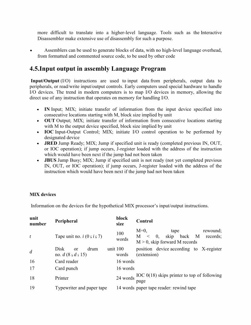
more difficult to translate into a higher-level language. Tools such as the Interactive Disassembler make extensive use of disassembly for such a purpose.
Assemblers can be used to generate blocks of data, with no high-level language overhead, from formatted and commented source code, to be used by other code
4.5.Input output in assembly Language Program
Input/Output (I/O) instructions are used to input data from peripherals, output data to peripherals, or read/write input/output controls. Early computers used special hardware to handle I/O devices. The trend in modern computers is to map I/O devices in memory, allowing the direct use of any instruction that operates on memory for handling I/O.
IN Input; MIX; initiate transfer of information from the input device specified into consecutive locations starting with M, block size implied by unit
OUT Output; MIX; initiate transfer of information from consecutive locations starting with M to the output device specified, block size implied by unit
IOC Input-Output Control; MIX; initiate I/O control operation to be performed by designated device
JRED Jump Ready; MIX; Jump if specified unit is ready (completed previous IN, OUT, or IOC operation); if jump occurs, J-register loaded with the address of the instruction which would have been next if the jump had not been taken
JBUS Jump Busy; MIX; Jump if specified unit is not ready (not yet completed previous IN, OUT, or IOC operation); if jump occurs, J-register loaded with the address of the instruction which would have been next if the jump had not been taken
MIX devices
Information on the devices for the hypothetical MIX processor‘s input/output instructions.
unit number Peripheral block
size Control
t Tape unit no. i (0 i 7) 100 words
M=0, tape rewound; M < 0, skip back M records; M > 0, skip forward M records
d Disk or drum unit no. d (8 d 15)
100 words
position device according to X-register (extension)
16 Card reader 16 words 17 Card punch 16 words
18 Printer 24 words IOC 0(18) skips printer to top of following page
19 Typewriter and paper tape 14 words paper tape reader: rewind tape
4.6.Assembly Programming tools
You can use an Integrated Development Environment to develop, assemble, and deploy Java Platform, Enterprise Edition (Java EE) modules forWebSphere® Application Server.
The IBM® Rational® Application Developer for WebSphere Software product, the IBM WebSphere Application Server Developer Tools for Eclipse product, and the IBM Assembly and Deploy Tools for WebSphere Administration product are supported tools for integrated development environments.
This information center refers to the products as the assembly tools. However, you can use the products to do more than assemble modules. Take advantage of these tools in an integrated development environment to develop, assemble, and deploy Java EE modules.
The Rational Application Developer for WebSphere Software is a more extensive set of tools supporting enterprise development. This workbench has integrated support for WebSphere Application Server Version 6.1 and later. This workbench also supports both the OSGi and Java EE programming models, and contains wizards and visual editors to help you develop Web 2.0, Service Component Architecture (SCA), Java, and Java EE applications. This product contains code quality tools to help you analyze code and improve performance. This product integrates with Rational Team Concert to provide a team-based environment to help developers share information and work collaboratively. The Trial download for Rational Application Developer is available at http://www.ibm.com/developerworks/downloads/r/rad/.
IBM WebSphere Application Server Developer Tools for Eclipse is a lightweight set of tools for developing, assembling, and deploying Java EE applications to WebSphere Application Server Version 7.0 and 8.0. This workbench integrates with the application server to help you to quickly deploy and test applications. This product contains wizards and visual editors that support the Java EE programming model.
IBM Assembly and Deploy Tools for WebSphere Administration, available with WebSphere Application Server, provides the tools for administrators to assemble and deploy Web, Java, Java EE, and OSGi applications to WebSphere Application Server Version 8.0.
For documentation on the tools, see "Rational Application Developer documentation." Topics on application assembly in this information center supplement that documentation.
Important: The assembly tools run on Windows and Linux Intel platforms. Users of WebSphere Application Server on all platforms must assemble their modules using an assembly tool
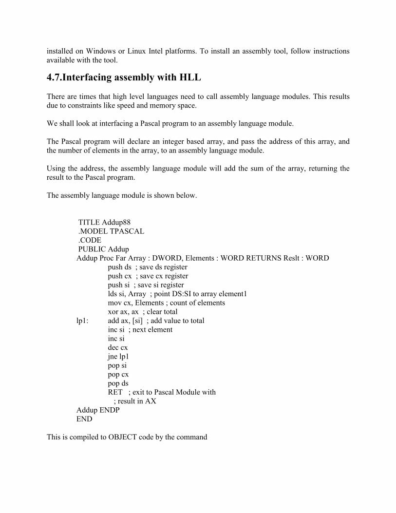
installed on Windows or Linux Intel platforms. To install an assembly tool, follow instructions available with the tool.
4.7.Interfacing assembly with HLL
There are times that high level languages need to call assembly language modules. This results due to constraints like speed and memory space.
We shall look at interfacing a Pascal program to an assembly language module.
The Pascal program will declare an integer based array, and pass the address of this array, and the number of elements in the array, to an assembly language module.
Using the address, the assembly language module will add the sum of the array, returning the result to the Pascal program.
The assembly language module is shown below.
TITLE Addup88 .MODEL TPASCAL .CODE PUBLIC Addup Addup Proc Far Array : DWORD, Elements : WORD RETURNS Reslt : WORD push ds ; save ds register push cx ; save cx register push si ; save si register lds si, Array ; point DS:SI to array element1 mov cx, Elements ; count of elements xor ax, ax ; clear total lp1: add ax, [si] ; add value to total inc si ; next element inc si dec cx jne lp1 pop si pop cx pop ds RET ; exit to Pascal Module with ; result in AX Addup ENDP END
This is compiled to OBJECT code by the command
$TASM ADDUP88
The Pascal module is shown below.
Program ADDDEMO (input, output); Uses DOS, CRT; Type IntArray = Array[1..20] of Integer; Var Numbers : IntArray; Result : Integer; Loop : Integer; {$F+} Function Addup( var Numbers : IntArray; Elements : Integer ) : Integer ; EXTERNAL; {$L ADDUP88.OBJ} {$F-} begin for loop:= 1 to 20 do Numbers[loop] := loop; Result := Addup( Numbers, 20 ); Writeln('The sum of the array is ', Result) End.
When compiled under Turbo Pascal, the two object modules are linked together, creating an executable file.
4.8.Device Deriver of assembly language
In another project for use with my notebook computer, I intend to build some sort of device which will interface to the parallel port, and provide additional, portable storage above and beyond the 720KB which can be accessed from each of the two floppy disks.
While I still am undecided about exactly how I will build such a device, or what it will be, I have started to look into the interface software for it, as I anticpate more problems there than actually constructing some sort of device. Much to my surprise, I have been able to find no information at all on the World-Wide Web on writing DOS device drivers, and I've been able to find any useful source code on the WWW to this date. However, after much searching, I finally stumbled across a fair amount of information in the back of the IBM MS-DOS Reference Manual, for IBM DOS V2.0 . This reference work seems to have all the information needed to create any device driver, for use with DOS. Sadly, it is out of print.
In the interests of furthuring the information available on the WWW, I decided to type in the source code given as an example. The manual has a source code listing for a RAMDisk device driver, which I present here.
This is the assembled listing: ibmvdisk.lst
This is assembly code, only: ibmvdisk.asm
A few quick notes about the code: You can save it after viewing it, using your browser's "Save As..." function.
I don't know what assembler this was written for: I present it here, as it was published. You will probably have to modify the source to work with your assembler.
4.9.Interrupts in assembly language programming
Interrupts in assembly language are a little trickier.
Since you have no idea of what the processor was doing when it was interrupted, you have no idea of the state of the W register, the STATUS flags, PCLATH or even what register page you are pointing to. If you need to alter any of these, and you probably will, you must save the current values so that you can restore them before allowing the processor to go back to what it was doing before it was so rudely interrupted. This is called saving and restoring the processor context.
If the processor context, upon return from the interrupt, is not left exactly the way you found it, all kinds of subtle bugs and even major system crashes can and will occur.
This of course means that you cannot even safely use the compiler=s internal variables for storing the processor context. You cannot tell which variables are in use by the library routines at any given time.
You should create variables in the PICBASIC PRO™ program for the express purpose of saving
W, the STATUS register and any other register that may need to be altered by the interrupt handler. These variables should not be otherwise used in the BASIC program.
While it seems a simple matter to save W in any RAM register, it is actually somewhat more complicated. The problem occurs in that you have no way of knowing what register bank you are pointing to when the interrupt happens. If you have reserved a location in Bank0 and the current register pointers are set to Bank1, for example, you could overwrite an unintended location. Therefore you must reserve a RAM register location in each bank of the device at the same offset.
As an example, let's choose the 16C74(A). It has 2 banks of RAM registers starting at $20 and $A0 respectively. To be safe, we need to reserve the same location in each bank. In this case we will choose the first location in each bank. A special construct has been added to the VAR command to allow this:
wsave var byte $20 system wsave1 var byte $a0 system
This instructs the compiler to place the variable at a particular location in RAM. In this manner, if the save of W "punches through" to another bank, it will not corrupt other data.
The interrupt routine should be as short and fast as you can possibly make it. If it takes too long to execute, the Watchdog Timer could timeout and really make a mess of things.
The routine should end with an Retfie instruction to return from the interrupt and allow the processor to pick up where it left off in your PICBASIC PRO™ program.
The best place to put the assembly language interrupt handler is probably at the very beginning of your PICBASIC PRO™ program. This should ensure that it is in the first 2K to minimize boundary issues. A GOTO needs to be inserted before it to make sure it won=t be executed when the program starts. See the example below for a demonstration of this.
If the PICmicro has more than 2K of code space, an interrupt stub is automatically added that saves the W, STATUS and PCLATH registers into the variables wsave, ssave and psave, before going to your interrupt handler. Storage for these variables must be allocated in the BASIC program:
wsave var byte $20 system wsave1 var byte $a0 system ' If device has RAM in bank1 wsave2 var byte $120 system ' If device has RAM in bank2 wsave3 var byte $1a0 system ' If device has RAM in bank3 ssave var byte bank0 system psave var byte bank0 system
You must restore these registers at the end of your assembler interrupt handler. If the PICmicro has 2K or less of code space, the registers are not saved. Your interrupt handler must save and restore any used registers.
Finally, you need to tell PBP that you are using an assembly language interrupt handler and where to find it. This is accomplished with a DEFINE:
DEFINE INTHAND Label
Label is the beginning of your interrupt routine. PBP will place a jump to this Label at location 4 in the PICmicro.
' Assembly language interrupt example led var PORTB.1 wsave var byte $20 system ssave var byte bank0 system psave var byte bank0 system Goto start ' Skip around interrupt handler ' Define interrupt handler define INTHAND myint ' Assembly language interrupt handler asm ; Save W, STATUS and PCLATH registers myint movwf wsave swapf STATUS, W clrf STATUS movwf ssave movf PCLATH, W movwf psave ; Insert interrupt code here ; Save and restore FSR if used bsf _led ; Turn on LED (for example) ; Restore PCLATH, STATUS and W registers movf psave, W movwf PCLATH swapf ssave, W movwf STATUS swapf wsave, F swapf wsave, W retfie endasm ' PICBASIC PRO™ program starts here start: Low led ' Turn LED off ' Enable interrupt on PORTB.0
INTCON = %10010000 loop: Goto loop ' Wait here till interrupted
Review Questions
1. What is assembly language programming? 2. Explain Input output in assembly Language Program? 3. Explain assembly language tool? 4. Describe the assembly language program in own words? 5. What is Interfacing assembly with HLL in details? 6. Explain Device drivers in assembly language? 7. Describe interrupt in assembly language programming? 8. What is modular programming? 9. Explain input output services in assembly language? 10. What is need of assembly language?

9, Km Milestone, NH-65, Kaithal - 136027, HaryanaWebsite: www.niilmuniversity.in
“The lesson content has been compiled from various sources in public domain including but not limited to the internet for the convenience of the users. The university has no proprietary right on the same.”


![Mercantile Law [Rai Foundation] - NIILM University](https://img.pdfslide.us/doc/110x75/61de2dc1925bc81c1c0ee188/mercantile-law-rai-foundation-niilm-university.jpg)