Embed Size (px)
Citation preview
Fundamental Defect Complexes and
Nanostructuring of Silicon by Ion Beams
by
Lasse Vines
Submitted
in partial fulfillment of the requirements
for the degree of
Philosophiae Doctor
Department of Physics
Faculty of Mathematics and Natural Sciences
University of Oslo
© Lasse Vines, 2008
Series of dissertations submitted to the Faculty of Mathematics and Natural Sciences, University of Oslo Nr. 703
ISSN 1501-7710
All rights reserved. No part of this publication may be reproduced or transmitted, in any form or by any means, without permission.
Cover: Inger Sandved Anfinsen. Printed in Norway: AiT e-dit AS, Oslo, 2008.
Produced in co-operation with Unipub AS. The thesis is produced by Unipub AS merely in connection with the thesis defence. Kindly direct all inquiries regarding the thesis to the copyright holder or the unit which grants the doctorate.
Unipub AS is owned by The University Foundation for Student Life (SiO)

To my grandfather
iii

AbstractSilicon technology has become a cornerstone for the technological advances in our
society for the last five decades. For carrying on with minimization of electronic devices
a huge effort has been directed toward the technological development and fundamental
understanding of physical processes associated with the ion implantation into silicon.
Indeed, in ion implantation the impurities are intentionally introduced into a matrix
lattice with the help of accelerated ion beams selectively modifying the properties
of the implanted area. In addition to the introduction of the doping impurity the
penetrating ions create defects that can be electrically active potentially affecting the
device performance. In spite of a long research activity in the field there are still several
open fundamental questions remaining, and this thesis contributes to the understanding
of ion implantation induced defect complexes in silicon.
Firstly, we have studied the electrical properties of vacancy type point defect com-
plexes generated in single collision cascades during heavy ion bombardment of sili-
con. Because of a high generation rate of defects within the “ion track” regions, a
characteristic pattern of nanochannels having modified Fermi levels due to the local
compensation around each ion trajectory is formed in n-type Si. The phenomenon has
been studied using spectroscopic and imaging techniques, specifically deep level tran-
sient spectroscopy (DLTS) and scanning capacitance microscopy (SCM). The SCM
measurements show a characteristic random pattern of reduced SCM signal correlated
with the density of the ion impacts. Moreover, a strong correlation is detected between
the probing frequency and the emission rate of the single negative acceptor level of
the divacancy (V2(−/0)) in Si. Further, DLTS reveals a significant filling time increase
for all electronic levels originated from vacancy complexes with increasing ion mass
as probed within the ion track regions. The results of isochronal annealing studies
of vacancy complexes generated by heavy ion implants are also explained in terms of
the revisited local compensation model. An improvement of the model is proposed,
where the divacancy is considered to be available in two fractions; (1) highly localized
v
vi Abstract
centers along the core track regions (V dense2 ) and (2) centers located outside ion tracks
(V dilute2 ). The relative abundance of V dense
2 /V dilute2 is ion mass dependent. In this model
the V dense2 fraction does not contribute to the doubly negative divacancy (V2(= /−))
signal due to local carrier compensation, and the DLTS amplitude of V2(= /−) is de-
termined only by the V dilute2 fraction. Our finding clarifies a long lasting discussion
in literature on the DLTS amplitude difference between V2(−/0) and V2(= /−) in ion
implanted n-type Si.
Secondly, the thesis contains an investigation of the dominant electron trap in p-
type Si (Ec−0.25eV ), where Ec is the conduction band edge. The Ec−0.25eV trap has
previously been ascribed to the boron interstitial-oxygen interstitial (BiOi) complex,
but our study shows no oxygen and only a weak boron dependence on the intensity of
the level, challenging the BiOi identification.
Finally, the thesis explores the use of defect engineering by introducing nano-
sized vacancy clusters (cavities) when synthesizing buried SiO2 by ion implantation
(SIMOX). Scanning spreading resistance microscopy measurements show that oxide
nucleation can be enhanced by introducing cavities, potentially reducing the required
oxygen dose during the SIMOX processing.
Acknowledgments
This thesis is the solid evidence of three years of research training in the physical
electronics group at the University of Oslo. A period which have been motivating, frus-
trating, educating, interesting, exhausting, stressful and exciting. Just as the athlete
depends on a good coach and a supporting team, the graduate student rely on good
advisers, supportive colleagues, friends and family in order to develop the necessary
research skills. I would therefore like to express my gratitude to my supervisors; my
main supervisor Andrej Yu. Kuznetsov for introducing me to this topic, and for his
enthusiasm for my work during the last three years, and my co-supervisors Bengt. G.
Svensson for his skillful and experienced supervision giving me the confidence in the
completion of this thesis, and Edouard V. Monakhov for his day to day supervision and
hands-on guidance, and for acting as Wikidepia on semiconductors when conventional
search methods failed.
I have also had the privilege to collaborate with Jens Jensen at Uppsala University,
who have conducted the impressively low dose implantations reported in this thesis
and added valuable contributions and inputs to my study, and Dr. Reinhard Kogler
at Forschungzentrum Rossendorf, who introduced me to defect engineering of SIMOX
processing and offered many inputs and interesting discussions. The in-house process-
ing could not have been carried out without the assistance from our dedicated engineers
in the MiNa lab, Viktor Bobal and Thomas Marthinsen. Thank you all!
I would also like to thank my colleagues at the MiNa lab; my “room mates” Klaus
M. Johansen and Mads Mikelsen, and the rest of the group for all the relevant and
irrelevant discussions, and for making my three years as a PhD student as interesting
and joyful as they have been.
Finally, I would like the thank my wife, Birgitte, for supporting me and challenging
me throughout my pregraduate, graduate and the coming postgraduate period, and
for making it all worthwhile.
vii

Contents
Abstract . . . . . . . . . . . . . . . . . . . . . . . . . . . . . . . . . . . . . . vAcknowledgments . . . . . . . . . . . . . . . . . . . . . . . . . . . . . . . . . viiTable of Contents . . . . . . . . . . . . . . . . . . . . . . . . . . . . . . . . . ixList of included papers . . . . . . . . . . . . . . . . . . . . . . . . . . . . . . xi
1 Introduction 1
2 Basics of charge carriers and point defects in semiconductors 52.1 Basics of charge carriers in semiconductors . . . . . . . . . . . . . . . . 5
2.1.1 The Poisson and continuity equations . . . . . . . . . . . . . . . 52.1.2 The drift-diffusion approximation . . . . . . . . . . . . . . . . . 62.1.3 The Fermi-level . . . . . . . . . . . . . . . . . . . . . . . . . . . 72.1.4 pn-junction . . . . . . . . . . . . . . . . . . . . . . . . . . . . . 8
2.2 Point defects in semiconductors . . . . . . . . . . . . . . . . . . . . . . 92.2.1 Formation of defects . . . . . . . . . . . . . . . . . . . . . . . . 92.2.2 Electrical properties of defects . . . . . . . . . . . . . . . . . . . 102.2.3 Shockley-Read-Hall statistics . . . . . . . . . . . . . . . . . . . 10
2.3 Device simulation using Technology Computer Aided Design (TCAD) . 12
3 Experimental techniques 153.1 Deep level transient spectroscopy . . . . . . . . . . . . . . . . . . . . . 15
3.1.1 Principle of operation . . . . . . . . . . . . . . . . . . . . . . . . 163.1.2 Obtaining electrical characteristics . . . . . . . . . . . . . . . . 18
3.1.2.1 Trap concentration . . . . . . . . . . . . . . . . . . . . 183.1.2.2 Depth profiling . . . . . . . . . . . . . . . . . . . . . . 193.1.2.3 Activation energy . . . . . . . . . . . . . . . . . . . . . 20
3.1.3 Minority carrier transient spectroscopy (MCTS) . . . . . . . . . 213.2 Electrical characterization using scanning probe microscopy . . . . . . . 22
3.2.1 Scanning spreading resistance microscopy . . . . . . . . . . . . . 233.2.1.1 Principle of operation . . . . . . . . . . . . . . . . . . 233.2.1.2 Quantification . . . . . . . . . . . . . . . . . . . . . . 263.2.1.3 Sample preparation . . . . . . . . . . . . . . . . . . . . 27
ix

x Contents
3.2.2 Scanning capacitance microscopy . . . . . . . . . . . . . . . . . 273.2.2.1 Principle of operation . . . . . . . . . . . . . . . . . . 273.2.2.2 Resolution . . . . . . . . . . . . . . . . . . . . . . . . . 293.2.2.3 Tip characteristics and sample preparation . . . . . . . 313.2.2.4 Towards quantitative SCM . . . . . . . . . . . . . . . 31
4 Point defects and ion induced nanostructuring in Si 334.1 Point defect structures after heavy ion implantation . . . . . . . . . . . 33
4.1.1 Motivation . . . . . . . . . . . . . . . . . . . . . . . . . . . . . . 334.1.2 Visualization . . . . . . . . . . . . . . . . . . . . . . . . . . . . 364.1.3 Simulation and annealing behavior . . . . . . . . . . . . . . . . 38
4.2 On the origin of the dominating electron trap in p-type Si . . . . . . . 394.3 Defect engineering of SIMOX structures . . . . . . . . . . . . . . . . . 43
5 Concluding remarks and suggestions for future work 47
Bibliography 51
List of included papers
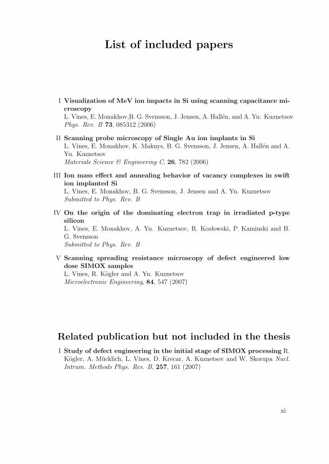
I Visualization of MeV ion impacts in Si using scanning capacitance mi-croscopyL. Vines, E. Monakhov,B. G. Svensson, J. Jensen, A. Hallen, and A. Yu. KuznetsovPhys. Rev. B 73, 085312 (2006)
II Scanning probe microscopy of Single Au ion implants in SiL. Vines, E. Monakhov, K. Maknys, B. G. Svensson, J. Jensen, A. Hallen and A.Yu. KuznetsovMaterials Science & Engineering C, 26, 782 (2006)
III Ion mass effect and annealing behavior of vacancy complexes in swiftion implanted SiL. Vines, E. Monakhov, B. G. Svensson, J. Jensen and A. Yu. KuznetsovSubmitted to Phys. Rev. B
IV On the origin of the dominating electron trap in irradiated p-typesiliconL. Vines, E. Monakhov, A. Yu. Kuznetsov, R. Koz�lowski, P. Kaminski and B.G. SvenssonSubmitted to Phys. Rev. B
V Scanning spreading resistance microscopy of defect engineered lowdose SIMOX samplesL. Vines, R. Kogler and A. Yu. KuznetsovMicroelectronic Engineering, 84, 547 (2007)
Related publication but not included in the thesis
I Study of defect engineering in the initial stage of SIMOX processing R.Kogler, A. Mucklich, L. Vines, D. Krecar, A. Kuznetsov and W. Skorupa Nucl.
Intrum. Methods Phys. Res. B, 257, 161 (2007)
xi


Chapter 1
Introduction
When an energetic heavy ion penetrates a solid target, it is slowed down by inter-
action with the target electrons and the target nuclei. The interaction between the
energetic ion and a target nucleus can be treated as a screened Coulomb scattering
event, that is an elastic collision between a moving ion and an atom at rest. The
interaction results in an energy transfer from the ion to the lattice atom. In crystals,
if the energy transfer is high enough, the atom can leave its lattice site and a Frenkel
pair, an atom at an interstitial site and a vacancy, is generated. After the generation,
both interstitials and vacancies can migrate, which can result in their annihilation or
formation of stable defect complexes and larger extended defects (e.g. dislocation loop,
cavities, etc.). The incident ion interacts also with both valence and core electrons of
the target. Due to the high mass ratio between ions and electrons and the large number
of interactions, a continuum approximation, where the ion is considered to move in a
viscous fluid, is usually applied.
Single crystalline silicon is a well known material, and is well suited for studying the
processes associated with the damage induced by heavy ions. Moreover, the methods
of ion implantation doping and synthesis are widely used in the electronic industry
further motivating the understanding of fundamentals of defect clustering reactions
in Si. For sufficiently low dose implantations, single collision cascades prevail in Si,
1
2 Chapter 1: Introduction
and implantation/irradiation of both electrons and heavy ions result in point defect
generation, rather than formation of extended defects. The “simplest” case of the
electron irradiation has been conveniently used for studying point defects in Si for
several decades due to the generation of a quite uniform distribution of vacancies
and self-interstitials (Frenkel pairs). For heavy ion implantation the generation of
Frenkel pairs is significantly stronger, resulting in a non-uniform defect profile around
the ion trajectory. It has been a longstanding discussion in the literature of how far
the implantation induced vacancies migrate before they form stable defect complexes
within and around the ion trajectory. In spite of considerable advances in theoretical
approaches, it is still difficult to perform reliable simulations of the defect reactions
induced by ion implantation since the time scale of the events spans from ∼ 10−12 s
to several minutes or days at room temperature. From an experimental point of view
no direct imaging of the electrically active defect distribution around an ion trajectory
in Si has been reported so far since the corresponding defect concentrations are below
the detection limit of conventional microscopy techniques motivating the introduction
of new techniques (Papers I and II). In addition, novel imaging techniques providing
not only structural but also functional (e.g. electrical) characterization of the samples
are interesting to apply when studying initial stages of ion implantation synthesis.
In addition to imaging techniques, there are also several spectroscopic methods
applicable to study point defects and defect clusters in Si. In this thesis the deep level
transient spectroscopy (DLTS) was employed, which is a well established technique for
investigation of electrically active defects in semiconductors. The studies are focused
on DLTS signatures of two charge states of a divacancy (two nearby vacancies forming a
stable configuration [1], V2) . Since the two charge states arise from the same defect, the
intensity of the DLTS signal for these states are expected to be the same. While the one-
to-one correlation holds for V2 formed by electron irradiation or light-ion implantation,
a deviation from the one-to-one correlation is observed for V2 formed by heavy ion
implantation. Several models have been proposed explaining the deviation. One model,
Chapter 1: Introduction 3
which has been explored in this thesis (Paper I-III), proposes that the local density
of the defects (specifically divacancies) within an ion track region is high enough to
cause local compensation and pinning of the Fermi-level to the deeper charge state of
V2, suppressing the filling of the shallower V2 state and reducing its DLTS intensity
(Paper III). This idea is interesting both for the fundamental understanding of the ion
induced damage in Si and for potential applications. Indeed, providing the local carrier
concentration around the ion trajectories is significantly altered compared to that in
the bulk, nanosized channels with a reduced carrier density are formed, consistent with
the interpretation of images in Paper I and II.
During the work on this thesis, several related findings and issues have occurred.
For example, while studying the divacancy in p-type Si, the behavior of the dominating
electron trap in boron doped material showed a boron dependence not previously re-
ported, suggesting that our understanding of interstitial related defects is incomplete.
This observation and its interpretation is pursued in Sec. 4.2 and Paper IV. More-
over, addressing the reactions resulting in extended defects the role of larger vacancy
clusters formed after the ion implantation was investigated. Specifically the influence
of cavities on the initial stages of ion implantation SiO2 synthesis was studied. This
topic is introduced and explored in Sec. 4.3 and Paper V.
The thesis is organized as follows: Chapter 2 introduces the basic equations for
understanding semiconductors and point defects in semiconductors, hereby forming
the basis for understanding Technology CAD simulations, which are presented at the
end of the chapter. Chapter 3 describes the experimental techniques used in this work,
while Chapter 4 highlights the work presented in the following papers.


Chapter 2
Basics of charge carriers and point
defects in semiconductors
This chapter presents the fundamental equations used in semiconductor physics,
and aims to serve as a basis for understanding the simulations carried out in the
attached papers, and the experimental methods used in this thesis.
2.1 Basics of charge carriers in semiconductors
2.1.1 The Poisson and continuity equations
The Poisson equation is a part of Maxwells equations and relates the change in
electrostatic potential, ∇Ψ, to the charge density. For a semiconductor it can be
defined as [2] [3]
∇ · ε∇Ψ = −q (p − n + Nd − Na) , (2.1)
where ε is the permittivity of the semiconductor, p is the hole density, n is the electron
density, Nd is the density of ionized donors, Na is the density of ionized acceptors, and q
is the elementary charge. The Poisson equation, together with the continuity equations
for electrons and holes, accounts for the transport of electrons and holes in and out of
5
6 Chapter 2: Basics of charge carriers and point defects in semiconductors
a region and for the generation or recombination of electron-hole pairs. They form a
powerful framework for understanding a variety of phenomena observed in solid state
electronics. The continuity equations [3] for electrons and holes are,
∇ ·−→J n = qR + q ∂n
∂t, (2.2)
−∇ ·−→J p = qR + q ∂p
∂t, (2.3)
where−→J n and
−→J p are the current densities for electrons and holes, respectively, and
R is the net electron-hole recombination rate. The Poisson equation and the transport
equations will constitute a set of differential equations to be solved. However, to suc-
cessfully solve these equations additional models are needed, that describe for example,
the electron-hole recombination R and the current densities.
2.1.2 The drift-diffusion approximation
Assuming that drift and diffusion of charge carriers are the main mechanisms for
charge transport, the so-called drift-diffusion approximation for the current densities
of electrons and holes can be described as [3]:
−→J n = qnμnE + qDn
dndx
, (2.4)
−→J p = qpμpE − qDp
dpdx
, (2.5)
where μn and μp are the electron and hole mobilities, respectively, Dn and Dp are the
diffusion coefficient of electrons and holes, respectively, and E is the electric field.
The mobility describes how easily an electron or a hole moves in the semiconduc-
tor when subjected to an electric field. In an intrinsic semiconductor the mobility
is limited by phonon scattering, which only depends on the temperature. In doped
semiconductors the scattering can also occur due to the carrier interaction with the
ionized impurities. Additionally, in high electric fields the carrier scattering related to
the field effect can become significant and must also be taken into consideration. In

Chapter 2: Basics of charge carriers and point defects in semiconductors 7
the present work, only the phonon scattering [4] and a model (the Masetti model [5])
for the impurity (dopant) scattering have been used.
The effective intrinsic density of e.g. electrons is related to the band gap of the
semiconductor, and can be calculated from ni,eff = ni exp ΔEg
2kBT[6] [7] if both doping
dependence and band gap narrowing are included, where ni is the intrinsic density for
an undoped semiconductor and given by ni =√
NC(T )NV (T ) exp−Eg
2kBT. Here, Eg is
the band gap, kB is Boltzmanns constant, T is the absolute temperature, ΔEg includes
the band gap narrowing effect, NC is the effective conduction band density of states,
and NV is the effective valence band density of states.
At room temperature, one can consider p- and n-type dopants in Si fully ionized.
Thus N+d = Nd and N−
a = Na for extrinsic semiconductors, and can be readily inserted
into Eq. 2.1. However, at reduced temperature some of the dopant atoms will not be
ionized, lowering the carrier concentration. The concentration of ionized donors, N+d
will be reduced with temperature according to [6] N+d = Nd
1+gD expEF −ED
kBT
, where gD is
the degeneracy factor and follows from the Fermi-Dirac distribution, ED is the donor
activation energy, and EF is the Fermi level.
2.1.3 The Fermi-level
The Fermi level (or Fermi energy) is related to the fact that electrons obey Fermi-
Dirac statistics, and represents an important quantity in semiconductor physics. The
Fermi-Dirac distribution function gives the probability that an available energy state
will be occupied by an electron, f(E) = 11+exp (E−EF )/kBT
. Hence, an energy state
at the Fermi level has the probability of 1/2 of being occupied by an electron [3].
However, in an ideal semiconductor there are no available states within the band gap,
and therefore no possibility of finding an electron there. Hence, the available states are
found in the tail of the distribution. The Fermi level for an intrinsic semiconductor is
located close to the middle of the bandgap, while for instance in a n-type semiconductor
the Fermi level is pushed towards the conduction band. Assuming that the Fermi level
8 Chapter 2: Basics of charge carriers and point defects in semiconductors
lies at least several kBT below the conduction band, one can approximate the carrier
concentration of e.g an n-type semiconductor as n = Nc exp−(Ec − EF )/kBT , where
Ec is the conduction band edge and Nc is the effective density of states in the conduction
band. In non-equilibrium situations, when the carriers are injected or generated, it is
not meaningful to use the Fermi level, thus quasi Fermi levels for electrons and holes
are frequently introduced instead.
2.1.4 pn-junction
When semiconductors of different conductivity are put together an equilibrium
solution would require that the Fermi level in the materials is constant. For example
in a pn-junction, carriers near the interface will diffuse over to the other side creating a
space charge region depleted of free charge carriers, or a depletion region if an abrupt
transition is assumed (the depletion approximation), in order to satisfy Eq. 2.1. Thus,
requiring charge neutrality, an expression for the width of the depletion region, W , in
a one dimensional structure can be stated as [3]
W =
√2ε(V0 − V )
q
Na + Nd
NdNa(2.6)
where V0 is the built in voltage and V is the applied voltage. A similar expression can
be found for a Schottky barrier, i.e. a rectifying semiconductor-metal contact. The
junction and its depletion region can be considered as a parallel plate capacitor, and
this concept is of uttermost importance both in semiconductor devices and in our case
in probing point defects in the band gap by e.g. deep level transient spectroscopy
(DLTS, see Sec. 3.1). The resulting capacitance, C, becomes
C =εA
W(2.7)
where A is the contact area.
Chapter 2: Basics of charge carriers and point defects in semiconductors 9
2.2 Point defects in semiconductors
2.2.1 Formation of defects
In our case of low dose ion implantation, the elastic collision between the energetic
ion and a host atom can result in vacancy (V) and interstitial (I) generation (Frenkel
pair) if the energy transfer is above a threshold value. Depending on the amount
of energy transfered between the initial ion and the lattice atom (the interstitial),
the interstitial can accelerate and collide with other lattice atoms, creating a collision
cascade. The collision cascades are more pronounced for heavier ions compared to
lighter ions and electron irradiation. In a collision cascade, two nearby vacancies can
for example form a divacancy (two nearby vacancies forming a stable configuration
V2 [1]), which is stable at room temperature. Such defect generation are spatially
correlated, and thus confined within the ion trajectory.
The primary defects, the vacancies and interstitials, are highly mobile at room
temperature, and will migrate around in the lattice, potentially forming defect com-
plexes with other defects or annihilate by e.g. a vacancy interstitial recombination or
at sinks (e.g. a surface). In fact, only a few percentage of the generated vacancies and
interstitials escape mutual recombination [8]. From the surviving V and I, a complex
hierarchy of competing reaction involving both interstitials and vacancies will evolve,
resulting in secondary defects. By secondary defects one usually refers to all irradiation
induced defects that are thermally stable at room temperature. The amount and iden-
tity of the irradiation induced defects depend on the material and type of irradiation,
in particular on the type and concentration of impurities.
During thermal treatments, a defect can either migrate or dissociate, resulting in
annealing of certain defects and formation of others. Thus, by careful examination
of the thermal evolution of a defect, insight about the nature (e.g. the kinetics) of a
defect can be obtained.

10 Chapter 2: Basics of charge carriers and point defects in semiconductors
2.2.2 Electrical properties of defects
Defects can have a significant influence on the properties of a semiconductor. A
defect, either extended (one to three dimensional structures) or not (zero dimensional
structure or point defect), alter the periodic potential of a crystal, which leads to
formation of additional electronic states. Defects can be defined as electrically active
or inactive. Electrically active defects form states in the forbidden band gap, which can
donate or accept electrons to/from the conduction band (EC) or valence band (EV ). If
the state is neutral when it is filled by an electron, and positive if the state is empty, it
is defined as a donor, while if the state is neutral when it is empty and negative when it
is filled by an electron, the state is called an acceptor. The donor or acceptor level can
occur close to the conduction or valence band edge, respectively, and is then called a
shallow state. States located further away from the band edges are usually called deep
levels, and can act as generation or recombination centers. It is primarily the shallow
levels that are used for doping of semiconductors. However, their electrical impact on a
device structure can be mainly handled through the equations in the previous section,
and are not the prime target here.
2.2.3 Shockley-Read-Hall statistics
Consider a point defect having a state in the band gap with an energy ET below the
conduction band. According to Shockley, Read [9] and Hall [10] this state can capture
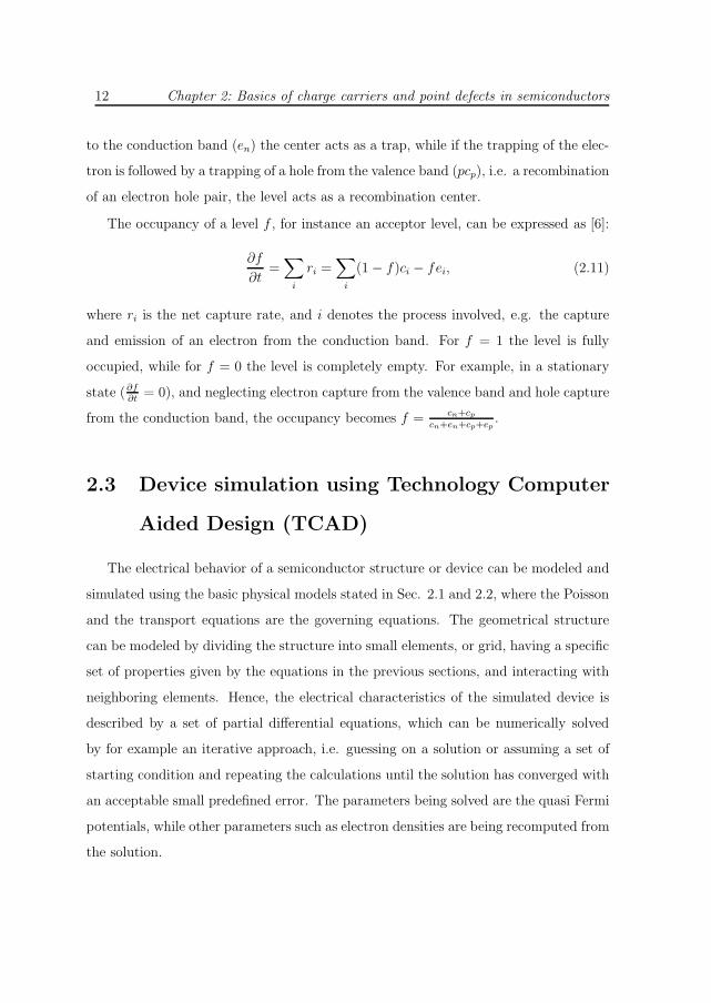
or emit an electron or hole from the conduction or valence band, respectively. Fig. 2.1
shows the charge interaction between the defect and the conduction and valence band.
Trapping of electrons from the conduction band and holes from the valence band occur
at rates of ncn and pcp, respectively, where cn is the electron capture coefficient and cp
is the hole capture coefficient. The capture coefficient can be defined as
cn(p) = σn(p)νth,n(p), (2.8)
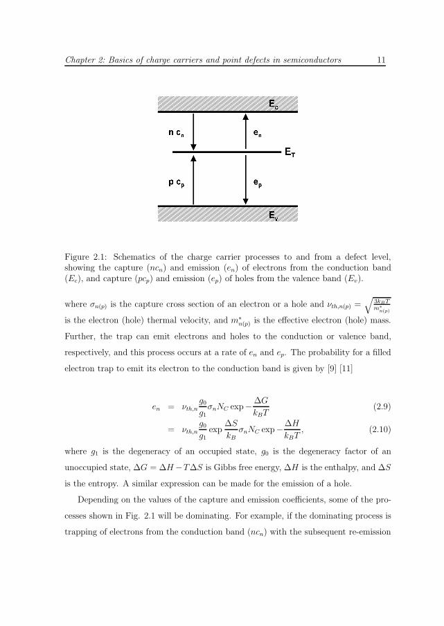
Chapter 2: Basics of charge carriers and point defects in semiconductors 11
Figure 2.1: Schematics of the charge carrier processes to and from a defect level,showing the capture (ncn) and emission (en) of electrons from the conduction band(Ec), and capture (pcp) and emission (ep) of holes from the valence band (Ev).
where σn(p) is the capture cross section of an electron or a hole and νth,n(p) =√
3kBTm∗
n(p)
is the electron (hole) thermal velocity, and m∗
n(p) is the effective electron (hole) mass.
Further, the trap can emit electrons and holes to the conduction or valence band,
respectively, and this process occurs at a rate of en and ep. The probability for a filled
electron trap to emit its electron to the conduction band is given by [9] [11]
en = νth,ng0
g1
σnNC exp−ΔG
kBT(2.9)
= νth,ng0
g1exp
ΔS
kBσnNC exp−
ΔH
kBT, (2.10)
where g1 is the degeneracy of an occupied state, g0 is the degeneracy factor of an
unoccupied state, ΔG = ΔH −TΔS is Gibbs free energy, ΔH is the enthalpy, and ΔS
is the entropy. A similar expression can be made for the emission of a hole.
Depending on the values of the capture and emission coefficients, some of the pro-
cesses shown in Fig. 2.1 will be dominating. For example, if the dominating process is
trapping of electrons from the conduction band (ncn) with the subsequent re-emission
12 Chapter 2: Basics of charge carriers and point defects in semiconductors
to the conduction band (en) the center acts as a trap, while if the trapping of the elec-
tron is followed by a trapping of a hole from the valence band (pcp), i.e. a recombination
of an electron hole pair, the level acts as a recombination center.
The occupancy of a level f , for instance an acceptor level, can be expressed as [6]:
∂f
∂t=
∑i
ri =∑
i
(1 − f)ci − fei, (2.11)
where ri is the net capture rate, and i denotes the process involved, e.g. the capture
and emission of an electron from the conduction band. For f = 1 the level is fully
occupied, while for f = 0 the level is completely empty. For example, in a stationary
state (∂f∂t
= 0), and neglecting electron capture from the valence band and hole capture
from the conduction band, the occupancy becomes f = cn+cp
cn+en+cp+ep.
2.3 Device simulation using Technology Computer
Aided Design (TCAD)
The electrical behavior of a semiconductor structure or device can be modeled and
simulated using the basic physical models stated in Sec. 2.1 and 2.2, where the Poisson
and the transport equations are the governing equations. The geometrical structure
can be modeled by dividing the structure into small elements, or grid, having a specific
set of properties given by the equations in the previous sections, and interacting with
neighboring elements. Hence, the electrical characteristics of the simulated device is
described by a set of partial differential equations, which can be numerically solved
by for example an iterative approach, i.e. guessing on a solution or assuming a set of
starting condition and repeating the calculations until the solution has converged with
an acceptable small predefined error. The parameters being solved are the quasi Fermi
potentials, while other parameters such as electron densities are being recomputed from
the solution.

Chapter 2: Basics of charge carriers and point defects in semiconductors 13
Several commercial software programs exist utilizing the physical and transport
equations as described above. In the work carried out in this thesis the device simulator
of Synopsys Technology CAD (TCAD) has been used. The development of TCAD
simulations started out in the late 1960’s to assist the growing bipolar technology,
and is still closely related to the IC industry. However, the basic principles of TCAD
make it a powerful tool for investigating and understanding fundamental semiconductor
properties and measurement results, for example the electrical behavior of a defect level
with a concentration having a non-uniform spatial distribution (Paper III).

Chapter 3
Experimental techniques
In this chapter, three methods for electrical characterization are presented. Deep
level transient spectroscopy (DLTS) is a macroscopic technique widely used in point
defect characterization, while both scanning spreading resistance microscopy (SSRM)
and scanning capacitance microscopy (SCM) are techniques for the nanometer scale,
mapping resistance and capacitance in two dimensions, respectively.
3.1 Deep level transient spectroscopy
Point defects are important from an application point of view due to their influence
on the electric current and capacitance performance of a device. On the other hand, this
performance modification can be utilized to study and extract fundamental informa-
tion about the crystal abnormalities and their electrical characteristics. For example,
by measuring the current or capacitance characteristics of a pn-diode or a Schottky
contact, the charge capture and emission properties, including activation energies, of
a point defect can be extracted.
In a depletion region of a pn-junction the free charge carriers are swept out by
the electric field arising between the two regions, as discussed in Sec. 2.1, resulting in
a region, W (Eq. 2.6), totally depleted of free charge carriers. Deep level transient
15
16 Chapter 3: Experimental techniques
spectroscopy (DLTS) [12] is an experimental technique utilizing the depletion region
capacitance modification in temperature and time domains as a function of applied
voltage providing information about electronic trap levels.
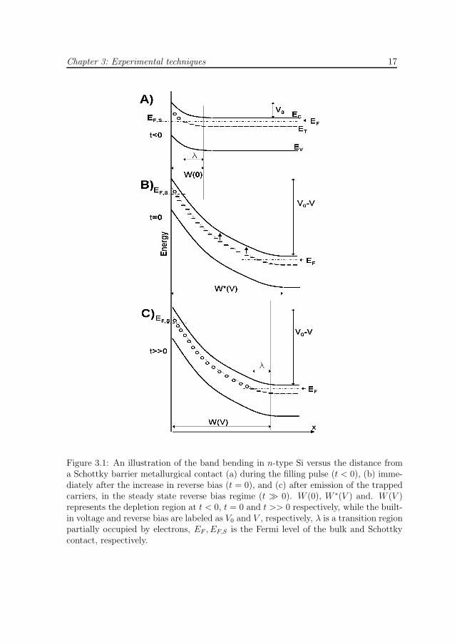
3.1.1 Principle of operation
In DLTS the applied bias voltage is alternately fixed between a smaller (filling
pulse) and a larger voltage (reverse bias). Consider a deep acceptor type electron trap
of concentration Nt, where Nt � n, close to a Schottky barrier in n-type Si. During
the filling pulse the steady state depletion width W (0) is small, where the defect levels
outside W (0) is below the Fermi level and will therefore trap charge (Fig. 3.1). After a
sudden increase in reverse bias the depletion region increases to W ∗(V ), and the traps
between W (0) and W ∗(V ) are arisen above the Fermi level (Fig. 3.1). At this moment,
the occupied traps start to release the electrons to the conduction band at a rate given
by Eq. 2.9. Due to the electric field the electrons will be swept away with a negligible
amount of re-trapping, and the depletion region will decrease, because of charge re-
distribution, to the steady state region, W (V ) (Fig. 3.1). λ is the width of the region
with partial filling of the trap level during the filling state of the measurement, Fig.
3.1, and given by λ =√
2ε(EF−ET )qNd
. The same arguments can also be made for pn-
junctions and donors and hole traps in p-type Si. Thus, the re-emission of carriers can
be detected by the influence on the junction capacitance through a transient detection
technique.
The measurements are carried out while scanning the appropriate temperature
range, changing the emission rate of the defect levels in accordance with Eq. 2.9,
and recording the capacitance transients by adjusting the temperature so that the
emission rate corresponds to a predefined time window, one has a mean to separate
the energy levels from each other in the form of characteristic peaks or signatures, as
illustrated in Fig. 3.2.
Chapter 3: Experimental techniques 17
Figure 3.1: An illustration of the band bending in n-type Si versus the distance froma Schottky barrier metallurgical contact (a) during the filling pulse (t < 0), (b) imme-diately after the increase in reverse bias (t = 0), and (c) after emission of the trappedcarriers, in the steady state reverse bias regime (t � 0). W (0), W ∗(V ) and. W (V )represents the depletion region at t < 0, t = 0 and t >> 0 respectively, while the built-in voltage and reverse bias are labeled as V0 and V , respectively, λ is a transition regionpartially occupied by electrons, EF , EF,S is the Fermi level of the bulk and Schottkycontact, respectively.
18 Chapter 3: Experimental techniques
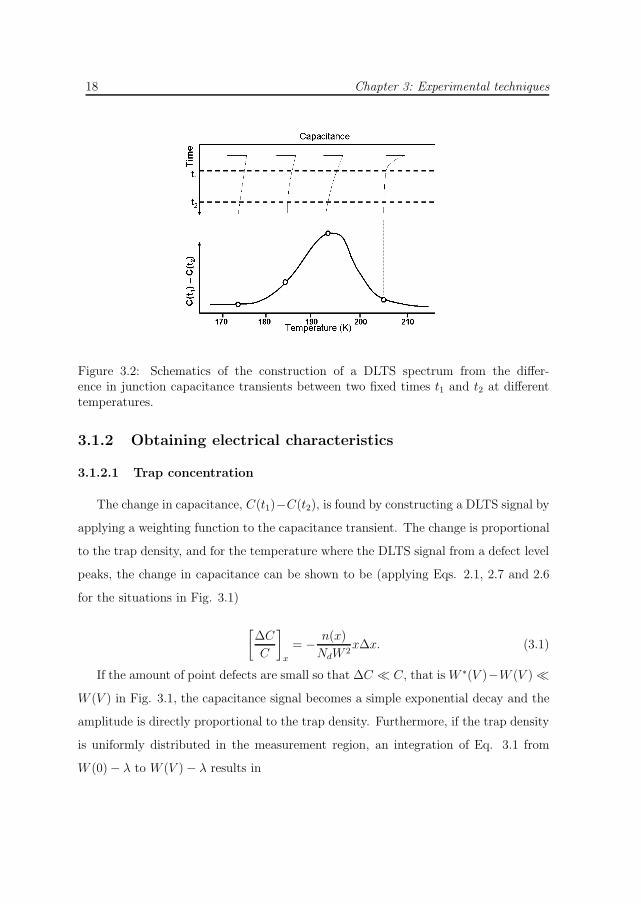
Figure 3.2: Schematics of the construction of a DLTS spectrum from the differ-ence in junction capacitance transients between two fixed times t1 and t2 at differenttemperatures.
3.1.2 Obtaining electrical characteristics
3.1.2.1 Trap concentration
The change in capacitance, C(t1)−C(t2), is found by constructing a DLTS signal by
applying a weighting function to the capacitance transient. The change is proportional
to the trap density, and for the temperature where the DLTS signal from a defect level
peaks, the change in capacitance can be shown to be (applying Eqs. 2.1, 2.7 and 2.6
for the situations in Fig. 3.1)
[ΔC
C
]x
= −n(x)
NdW 2xΔx. (3.1)
If the amount of point defects are small so that ΔC � C, that is W ∗(V )−W (V ) �
W (V ) in Fig. 3.1, the capacitance signal becomes a simple exponential decay and the
amplitude is directly proportional to the trap density. Furthermore, if the trap density
is uniformly distributed in the measurement region, an integration of Eq. 3.1 from
W (0) − λ to W (V ) − λ results in
Chapter 3: Experimental techniques 19
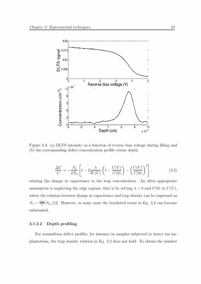
Figure 3.3: (a) DLTS intensity as a function of reverse bias voltage during filling and(b) the corresponding defect concentration profile versus depth.
ΔC
C= −
Nt
2Nd
[1 − 2
λ
W (V )
(1 −
C(V )
C(0)
)−
(C(V )
C(0)
)2]
, (3.2)
relating the change in capacitance to the trap concentration. An often appropriate
assumption is neglecting the edge regions, that is by setting λ = 0 and C(0) � C(V ),
where the relation between change in capacitance and trap density can be expressed as
Nt = 2ΔCC
Nd [12]. However, in some cases the bracketed terms in Eq. 3.2 can become
substantial.
3.1.2.2 Depth profiling
For nonuniform defect profiles, for instance in samples subjected to heavy ion im-
plantations, the trap density relation in Eq. 3.2 does not hold. To obtain the number
20 Chapter 3: Experimental techniques
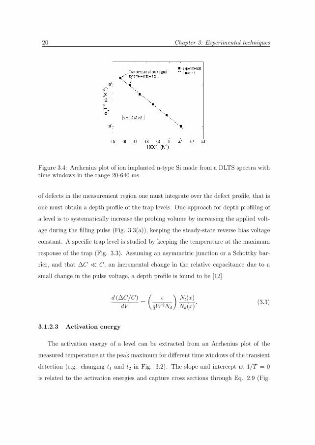
Figure 3.4: Arrhenius plot of ion implanted n-type Si made from a DLTS spectra withtime windows in the range 20-640 ms.
of defects in the measurement region one must integrate over the defect profile, that is
one must obtain a depth profile of the trap levels. One approach for depth profiling of
a level is to systematically increase the probing volume by increasing the applied volt-
age during the filling pulse (Fig. 3.3(a)), keeping the steady-state reverse bias voltage
constant. A specific trap level is studied by keeping the temperature at the maximum
response of the trap (Fig. 3.3). Assuming an asymmetric junction or a Schottky bar-
rier, and that ΔC � C, an incremental change in the relative capacitance due to a
small change in the pulse voltage, a depth profile is found to be [12]
d (ΔC/C)
dV=
(ε
qW 2Nd
)Nt(x)
Nd(x). (3.3)
3.1.2.3 Activation energy
The activation energy of a level can be extracted from an Arrhenius plot of the
measured temperature at the peak maximum for different time windows of the transient
detection (e.g. changing t1 and t2 in Fig. 3.2). The slope and intercept at 1/T = 0
is related to the activation energies and capture cross sections through Eq. 2.9 (Fig.
Chapter 3: Experimental techniques 21
3.4). Rewriting Eq. 2.9 to the form ln (en/T 2) = ln (σ∞Q) − ΔH/kBT , where Q is a
constant factor, one can readily obtain the activation energy (ΔH) from the slope in the
Arrhenius plot and the effective capture cross section (σ∞) from the extrapolated offset
of this line at 1/T = 0. However, a more accurate and direct method for measuring the
capture cross section, or in general studying the filling of a defect level, is by measuring
the filling time of a trap level. The filling time can be measured by increasing the
duration of the filling pulse while monitoring the DLTS signal keeping the temperature
constant at the DLTS peak maximum for the given defect level. For example, during
the filling of an electron trap (in n-type) the amount of trapped charge will in a first
approximation be NT f = NT [1 − exp (−cnt)], where the capture cross section can be
extracted from the capture coefficient according to Eq. 2.8.
3.1.3 Minority carrier transient spectroscopy (MCTS)
DLTS is used to obtain information about electrically active majority carrier traps,
but information about minority carrier traps can also be extracted. If a net forward bias
of a pn-junction is allowed during the filling pulse, minority carriers are injected and can
get trapped, and remitted again during the transient capacitance capture period. This
version of DLTS is called minority carrier transient spectroscopy (MCTS). Minority
carriers can also be generated optically (ODLTS) [11]. In MCTS, the injection of
carriers will not be limited by the doping concentration, but by the barrier height, and
by the diffusion length of the minority carriers. In addition, since a forward bias is
used during the filling pulse, the near surface region (Fig. 3.1) will also be filled and
contribute to the overall trap concentration. Both majority and minority carriers are
present in the sample during the filling pulse. Hence the minority carrier trapping level
must have a significantly larger minority capture cross section than majority carrier
capture cross section. Otherwise an electron-hole recombination will dominate over
re-emission and the trap level will be “unsaturable”, and therefore difficult to observe
in the MCTS spectrum.
22 Chapter 3: Experimental techniques
3.2 Electrical characterization using scanning probe
microscopy
Scanning probe microscopy (SPM) is a family of related techniques based on the
scanning of a sharp probe tip over a sample surface while measuring material properties
such as topography, electrical and/or magnetic characteristics. SPM originates from
the development of the scanning tunneling microscope by Binning and Rohrer in 1981
[13] and later the atomic force microscope by Binning, Quate and Gerber in 1986 [14].
In STM the tunneling of electrons between a tip and a sample is utilized in keeping
a constant separation while scanning the tip, in which a two-dimensional profile of
the surface topography at the atomic scale is extracted. The technique requires a
conductive sample surface, in addition to very stable measuring conditions, and is
therefore usually operated in ultra high vacuum conditions (UHV). The strict sample
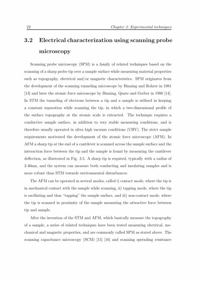
requirements motivated the development of the atomic force microscope (AFM). In
AFM a sharp tip at the end of a cantilever is scanned across the sample surface and the
interaction force between the tip and the sample is found by measuring the cantilever
deflection, as illustrated in Fig. 3.5. A sharp tip is required, typically with a radius of
2-40nm, and the system can measure both conducting and insulating samples and is
more robust than STM towards environmental disturbances.
The AFM can be operated in several modes, called i) contact mode, where the tip is
in mechanical contact with the sample while scanning, ii) tapping mode, where the tip
is oscillating and thus “tapping” the sample surface, and iii) non-contact mode, where
the tip is scanned in proximity of the sample measuring the attractive force between
tip and sample.
After the invention of the STM and AFM, which basically measure the topography
of a sample, a series of related techniques have been tested measuring electrical, me-
chanical and magnetic properties, and are commonly called SPM as stated above. The
scanning capacitance microscopy (SCM) [15] [16] and scanning spreading resistance
Chapter 3: Experimental techniques 23
Figure 3.5: Schematics of the AFM principle, where a tip at the end of a cantileveris scanned over the sample surface. The cantilever deflection, and thus the surfacetopography, is monitored using the reflection from a leaser beam.
microscopy (SSRM) [17] are particularly interesting in measuring/imaging electrical
properties of semiconductors.
3.2.1 Scanning spreading resistance microscopy
3.2.1.1 Principle of operation
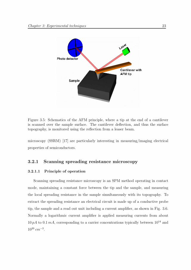
Scanning spreading resistance microscopy is an SPM method operating in contact
mode, maintaining a constant force between the tip and the sample, and measuring
the local spreading resistance in the sample simultaneously with its topography. To
extract the spreading resistance an electrical circuit is made up of a conductive probe
tip, the sample and a read out unit including a current amplifier, as shown in Fig. 3.6.
Normally a logarithmic current amplifier is applied measuring currents from about
10 pA to 0.1 mA, corresponding to a carrier concentrations typically between 1014 and
1020 cm−3.
24 Chapter 3: Experimental techniques
Figure 3.6: Illustration of the electrical circuit utilized in SSRM measurements, indi-cating different resistance contributions
For a conductive AFM tip in direct contact with a semiconductor the resistance,
Rtot, of the system is given by:
Rtot = Rs + Rc + Rtip + Rbulk, (3.4)
where Rs is the spreading resistance, Rc is the contact resistance, Rtip is the resistance
of the probe tip, and Rbulk includes the bulk resistance, the back contact resistance
and the resistance in the readout unit.
The spreading resistance is related to the resistivity ρ of the material, and hence
the carrier concentration through the equations
Rs =ρ
Atip, (3.5)
1
ρ= σ = qnμn + qpμp, (3.6)
(3.7)
Chapter 3: Experimental techniques 25
assuming an ideal ohmic contact, where ρ is the resistivity of the sample and Atip is the
effective contact size, and σ is the conductivity. For a cylindrical contact Atip = 4×rcyl
[18], where Rcyl is the radius of the cylinder, while Atip = 2π× rhem [18] for a probe tip
shaped as a hemisphere with radius rhem. Since the radius of the tip is small, typically
10−40nm, Rs is large and can dominate the total resistance if the other contributions
in Eq. 3.4 are kept sufficiently low. Hence, in a well designed experiment the SSRM
resistance is inversely proportional to the carrier concentration. Moreover, Eq. 3.7 can
be used as a first order approximation to quantify the carrier concentration.
To obtain a low contact resistance, Rc, a large force between the tip and sample is
applied, typically in the range of 1−50μN , penetrating any oxide layer and plastically
deforming the Si region underneath [19]. The tip will therefore scratch the sample
making repeating scans in the same region difficult. To have a low probe resistance,
Rtip, the conductivity of the probe tip must be high. In addition, the probe tip should
ideally be sharp to give a high lateral resolution, hard enough to withstand the high
pressures between tip and sample, and preferably very resistant to wear and tear.
Typical probes used in SSRM are etched Si tips coated with doped diamond or metal
(e.q. an inner layer of Ti and an outer layer of Pt), where the doped diamond tips are
preferred in studies of Si samples. However, the probe resistance of the doped diamond
tips can influence measurements on low resistivity samples [19]. The bulk resistance
term in Eq. 3.4, Rbulk, includes both the bulk resistivity of the sample, the contact
resistance of the back contact and the resistivity of the readout unit, and must also be
kept sufficiently low.
Additional complications of the conversion of SSRM resistance into sample resis-
tivity or carrier concentrations arise since a scanning nanosized electrical contact is
rarely ohmic, and the measured resistance will therefore depend on the applied bias
requiring the recording of a structure at several bias voltages. Secondly, the contact
size is difficult to determine, both because the tip size changes between tips and after
tip wear, and because the effective electrical contact size can differ from the geometrical
26 Chapter 3: Experimental techniques
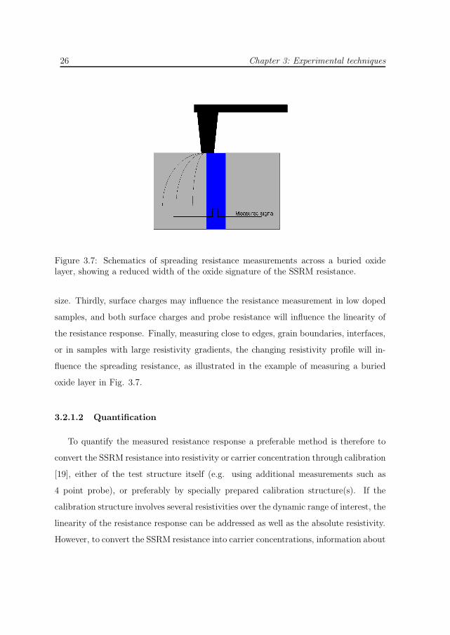
Figure 3.7: Schematics of spreading resistance measurements across a buried oxidelayer, showing a reduced width of the oxide signature of the SSRM resistance.
size. Thirdly, surface charges may influence the resistance measurement in low doped
samples, and both surface charges and probe resistance will influence the linearity of
the resistance response. Finally, measuring close to edges, grain boundaries, interfaces,
or in samples with large resistivity gradients, the changing resistivity profile will in-
fluence the spreading resistance, as illustrated in the example of measuring a buried
oxide layer in Fig. 3.7.
3.2.1.2 Quantification
To quantify the measured resistance response a preferable method is therefore to
convert the SSRM resistance into resistivity or carrier concentration through calibration
[19], either of the test structure itself (e.g. using additional measurements such as
4 point probe), or preferably by specially prepared calibration structure(s). If the
calibration structure involves several resistivities over the dynamic range of interest, the
linearity of the resistance response can be addressed as well as the absolute resistivity.
However, to convert the SSRM resistance into carrier concentrations, information about
Chapter 3: Experimental techniques 27
the mobility is necessary (Eq. 3.7).
3.2.1.3 Sample preparation
The sample preparation procedures depend on the material and application. Plan
view measurements are relatively straight forward, where an oxide removal and back
side contact formation using a conductive glue are normally sufficient. For cross section
measurements, standard procedures have been developed for Si [19], involving cleaving,
mounting on support structure, polishing and back contact formation. However, for
other materials, such as e.g. ZnO and InP, and in some Si studies a simple cleaving
and backside contact formation can be sufficient.
3.2.2 Scanning capacitance microscopy
Scanning capacitance microscopy (SCM) is operated in contact mode, but in con-
trast to SSRM, it measures the changes in capacitance instead of resistance.
3.2.2.1 Principle of operation
The measurements rely on a metal-insulator-semiconductor (MIS) structure, as
illustrated in Fig. 3.8 where the conductive tip represents the metal, and an oxide
usually represents the insulator. Hence, the tip operated in SCM mode does not
penetrate the oxide layer. In an ideal one dimensional system, the total capacitance
Ctot of the MIS/MOS structure is the series combination of the oxide capacitance Cox
and the semiconductor capacitance Cs
1
Ctot=
1
Cox+
1
Cs. (3.8)
In the depletion approximation, the oxide and the semiconductor can be character-
ized using a parallel plate capacitor, as described in Sec. 2.1, that is Cox =εoxAtip
doxand
28 Chapter 3: Experimental techniques
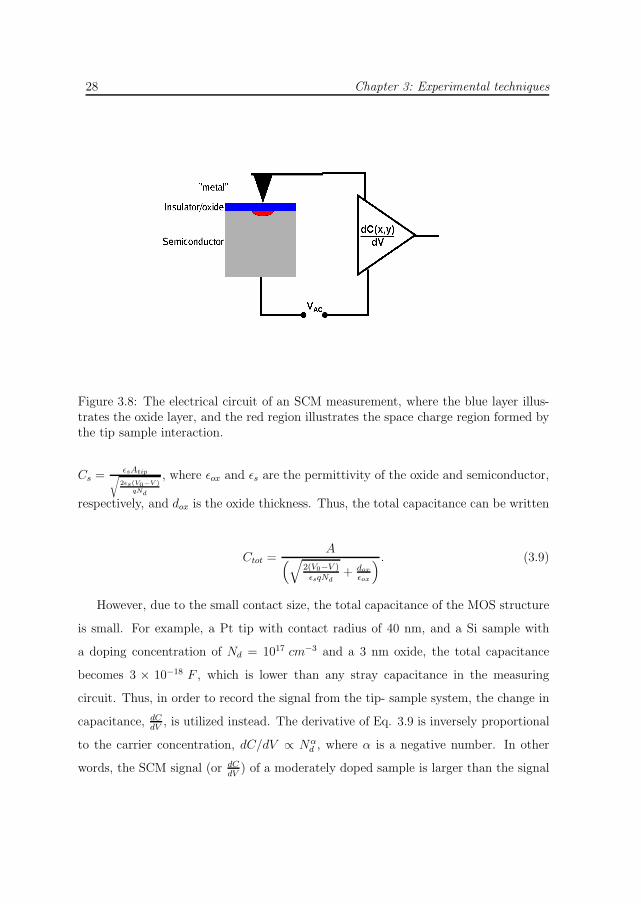
Figure 3.8: The electrical circuit of an SCM measurement, where the blue layer illus-trates the oxide layer, and the red region illustrates the space charge region formed bythe tip sample interaction.
Cs =εsAtipr2εs(V0−V )
qNd
, where εox and εs are the permittivity of the oxide and semiconductor,
respectively, and dox is the oxide thickness. Thus, the total capacitance can be written
Ctot =A(√
2(V0−V )εsqNd
+ dox
εox
) . (3.9)
However, due to the small contact size, the total capacitance of the MOS structure
is small. For example, a Pt tip with contact radius of 40 nm, and a Si sample with
a doping concentration of Nd = 1017 cm−3 and a 3 nm oxide, the total capacitance
becomes 3 × 10⁻¹⁸ F , which is lower than any stray capacitance in the measuring
circuit. Thus, in order to record the signal from the tip- sample system, the change in
capacitance, dCdV
, is utilized instead. The derivative of Eq. 3.9 is inversely proportional
to the carrier concentration, dC/dV ∝ Nαd , where α is a negative number. In other
words, the SCM signal (or dCdV
) of a moderately doped sample is larger than the signal
Chapter 3: Experimental techniques 29
from a highly doped sample. Moreover, as seen from Eq. 3.9, the SCM signal is
independent of the mobility, in contrast to other measuring techniques such as SSRM.
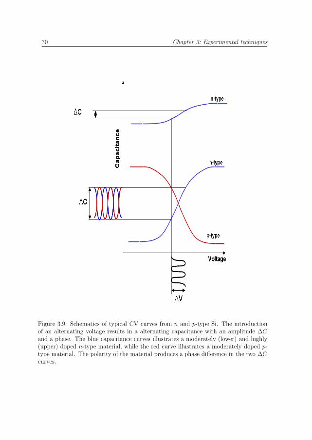
To elaborate on the properties of the SCM (dC/dV ) signal, let us consider the typ-
ical capacitance-voltage (CV) curve for a moderately doped p-channel (n-substrate)
MOS structure as shown by the (lower) blue curve in Fig. 3.9. Applying an alternat-
ing voltage using a moderate frequency (∼ 50− 100 kHz) and with an amplitude ΔV
superimposed on a dc voltage, the MOS structure is alternating between weak accumu-
lation and depletion. The resulting change in capacitance is measured, ΔC (see Fig.
3.9), using an ultra high frequency (∼ 1GHz) capacitance meter [20]. To maximize
the output signal the dc bias voltage is operated around the flat band voltage. Hence,
for a low and moderately doped semiconductor the amplitude of ΔC is large compared
to a highly doped material, Fig. 3.9.
Further, the phase of the measured ΔC compared to ΔV can be used to distinguish
p-type and n-type material, due to the polarity change in the MOS structure, as illus-
trated by the blue and red ΔC line in Fig. 3.9. Hence, a 180◦ phase shift is observed
between n and p-type material.
In the discussion above a MOS structure has been assumed. However, SCM mea-
surements can also be carried out on samples without an oxide layer if a Schottky
barrier with sufficient quality is established between the tip and the sample.
3.2.2.2 Resolution
The resolution in SCM is related to the probing volume formed by the space charge
region underneath the tip [21] (see the red region in Fig. 3.8). The fundamental
limitation is given by the screening length of the charge carriers, the Debye length [22],
given by LD =√
εskBTq2n
. However, a practical length scale limitation is given by the
width of the depletion region (see Eq. 2.6). Naturally, the resolution depends on the
applied bias and the carrier concentration. For example, Si with doping concentration
1018 cm−3 the screening length and the depletion width would be about 4 and 20 nm,
30 Chapter 3: Experimental techniques
Figure 3.9: Schematics of typical CV curves from n and p-type Si. The introductionof an alternating voltage results in a alternating capacitance with an amplitude ΔCand a phase. The blue capacitance curves illustrates a moderately (lower) and highly(upper) doped n-type material, while the red curve illustrates a moderately doped p-type material. The polarity of the material produces a phase difference in the two ΔCcurves.
Chapter 3: Experimental techniques 31
respectively, while in low doped samples, e.g. Nd = 1015 cm−3, the corresponding
numbers would be ∼ 130 and 670 nm. However, taking the tip radius and shape into
account, the lateral resolution can be considered as a convolution between the tip size
and the depletion region. Thus, in materials with a high doping concentration the tip
radius can significantly influence the lateral resolution, while in low doped materials
the resolution, both laterally and in depth, would be given by the depletion region.
3.2.2.3 Tip characteristics and sample preparation
The main difference between the tips used in SSRM and SCM is the force constant of
the cantilever on which the tip is mounted. In SCM this force constant is approximately
one order of magnitude lower, reducing the applied force between the tip and the
sample, and hence, not penetrating the oxide layer. Thus, both the surface roughness
and oxide are important in obtaining good quality measurements. Procedures for
sample preparation have therefore been developed [20], where a routine procedure
for cross section measurements include stacking, sawing, gluing and polishing steps, in
addition to low temperature oxidation to control the thermal oxide. Similar procedures
can be carried out for plan view measurements as well. However, depending on the
initial wafer quality and amount of processing steps applied to the structure, some
steps can be omitted.
3.2.2.4 Towards quantitative SCM
A non-linear expression relating the carrier concentration and the dC/dV ampli-
tude of the SCM signal can be found from the one dimensional expression in Eq. 3.9.
However, a SCM measurement is three dimensional in nature, complicating the simple
expression in Eq. 3.9. Moreover, the three dimensional tip shape must be included
for a proper evaluation of the resulting SCM signal, in addition to the uncertainties
in uniformity and size of the oxide layer. Thus, traditionally SCM has been used as
qualitative tool, and this is also the case for the work reported in this thesis. However,

32 Chapter 3: Experimental techniques
efforts have been made developing SCM into a quantitative tool [16]. In the recent
years encouraging results have been obtained for well controlled test samples using a
calibration curve method [23], where the calibration curves are developed using ref-
erence samples and SCM simulation software. It is also worthwhile to mention that
observations of spatial feature sizes down to 1nm have been reported [22]. Anyhow,
the most crucial reason for using SCM in the present thesis is the ability to record local
charge influencing the depletion region capacitance.

Chapter 4
Point defects and ion induced
nanostructuring in Si
This chapter aims to provide a short description of the studies that have been
performed and highlight the main results obtained. The first section is devoted to the
fundamental study of local compensation after heavy ion impacts in n-type Si. The
second section focus on the nature of the dominating electron trap observed in p-type
Si, while the third section is devoted to the investigation of the role of large vacancy
clusters and cavities on the initial stages of ion implantation synthesis of SiO2.
4.1 Point defect structures after heavy ion implan-
tation
4.1.1 Motivation
There is a longstanding discussion in the literature of how far the irradiation/implantation
induced vacancies can migrate at room temperature in Si before they form stable defect
complexes, e.g. the divacancy V2. In ion irradiated samples, the vacancies are formed
within a narrow region around the ion trajectory, as estimated by TRIM [24]. The
33
34 Chapter 4: Point defects and ion induced nanostructuring in Si
divacancy can form both by direct interaction when two consecutive Si atoms are dis-
placed by the impinging ion [1], and by pairing of two migrating monovacancies [25].
V2 is one of the most fundamental, and one of the most disputed, defect complexes
occurring after electron and ion irradiation, having two negative charge states in the
band gap. Its doubly negative charge state, V2(= /−), was identified due to its 1:1
correlation with the singly negative charge state (V2(−/0)) after electron irradiation
[26]. However, a deviation from this 1:1 correlation was observed, when bombarding
with protons and α-particles [27], and heavier ions [28]. Several models were intro-
duced to explain this deviation, including (i) strain in the heavy ion collision cascades
preventing the motional averaging of the V2 state favoring V2(−/0) over V2(= /−) [28]
[8] [29], (ii) additional levels e.g. larger vacancy clusters (Vx, x > 2) contributing to
the DLTS intensity at Ec−0.42eV [30], and (iii) local carrier compensation due to high
divacancy concentration ([V2]) around the ion trajectory so that much less electrons are
available to fill the doubly negative state [31] [32] [33]. For the latter model, the local
compensation model, the observed DLTS behavior has been linked to the migration
length of irradiation generated vacancies [32].
To motivate the idea of the local compensation, assume a 600keV Si impact in Si,
creating a maximum of 7 vacancies/ion/nm, as found by averaging over 400 impacts
using TRIM simulations (using a displacement energy of 15 eV ). Presuming only 1%
[8] of the generated vacancies form V2, and that the migration length is less than 15nm
(Paper III), the peak V2 concentration becomes ∼ 1017 cm−3, which is higher than
most of the doping concentrations used in DLTS studies. For a higher concentration
of deep acceptors than shallow donors, a depletion of carriers is expected, pinning
the Fermi-level at the deep acceptor state, and developing an energy barrier around
the disordered region, as illustrated in Fig. 4.1(a). Thus, the barrier will lower the
amount of electrons available for occupying states closer to the conduction band, such as
V2(= /−). However, this pinning will be local, and the surrounding matrix will modify
the local compensation by supplying additional charge, as seen in Fig. 4.1(b) for the
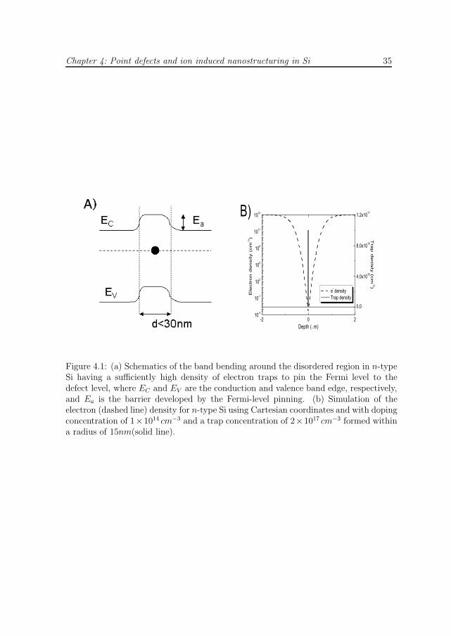
Chapter 4: Point defects and ion induced nanostructuring in Si 35
Figure 4.1: (a) Schematics of the band bending around the disordered region in n-typeSi having a sufficiently high density of electron traps to pin the Fermi level to thedefect level, where EC and EV are the conduction and valence band edge, respectively,and Ea is the barrier developed by the Fermi-level pinning. (b) Simulation of theelectron (dashed line) density for n-type Si using Cartesian coordinates and with dopingconcentration of 1×1014 cm−3 and a trap concentration of 2×1017 cm−3 formed withina radius of 15nm(solid line).
36 Chapter 4: Point defects and ion induced nanostructuring in Si
defect channel estimated above, and with a bulk doping concentration of 1×1014 cm−3.
The distribution of the space charge region around the ion trajectory will depend on
both the defect concentration and the bulk doping concentration. In the example at
hand, Fig. 4.1(b), the radius of the space charge region is on the order of ∼ 500nm.
4.1.2 Visualization
The discussion of defect production from ion impacts are mainly based on DLTS
studies. DLTS is a macroscopic measurement technique [12], where the capacitance
transients over a large (typically > 1 × 10⁻² cm2) area are recorded. To verify a local
compensation effect, i.e. the fact that the defect distribution after heavy ion impacts
are highly nonuniform and can significantly alter the local charge concentration, a
microscopic technique would be beneficial. With the advances in atomic force mi-
croscopy (AFM), in particular with the development of scanning spreading resistance
microscopy (SSRM) and scanning capacitance microscopy (SCM), such opportunities
become available. SCM measures the change in local capacitance in the near surface re-
gion of a sample, see Sec. 3.2.2, and can be utilized for visualizing the local distribution
of charge concentration.
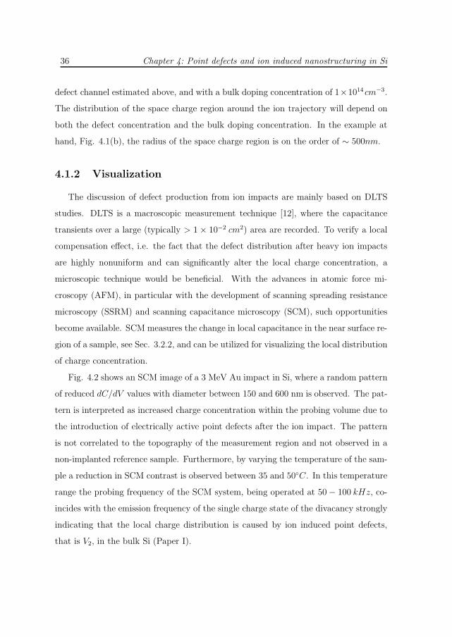
Fig. 4.2 shows an SCM image of a 3 MeV Au impact in Si, where a random pattern
of reduced dC/dV values with diameter between 150 and 600 nm is observed. The pat-
tern is interpreted as increased charge concentration within the probing volume due to
the introduction of electrically active point defects after the ion impact. The pattern
is not correlated to the topography of the measurement region and not observed in a
non-implanted reference sample. Furthermore, by varying the temperature of the sam-
ple a reduction in SCM contrast is observed between 35 and 50◦C. In this temperature
range the probing frequency of the SCM system, being operated at 50 − 100 kHz, co-
incides with the emission frequency of the single charge state of the divacancy strongly
indicating that the local charge distribution is caused by ion induced point defects,
that is V2, in the bulk Si (Paper I).
Chapter 4: Point defects and ion induced nanostructuring in Si 37
Figure 4.2: SCM image of a 3 MeV Au impact in n-type Si (doping 1 × 1016 cm−3).
The SCM results also show a distinct dose dependence, where the number of features
are significantly lower than the number of ion impacts. For example, from 3 MeV Au
impacts in Si no features are observed for impact doses lower than 2× 108 cm−2, while
a dose of 8 × 108 cm−2 showed approximately 20 features, and a dose of 5 × 109 cm−2
showed 60 features. However, the probing volume is, as discussed in Sec. 3.2.2, related
to the screening length, or the depletion region. Thus, the SCM measurements will
show the convolution between a relatively large probing volume and the defect size.
Several models can explain this non-linear dose dependence, for example the amount of
induced defects in the near-surface regions varies resulting in only a fraction of tracks
visible by SCM, or several nearby tracks are necessary to exceed the upper noise level
of the system (Paper II).
An alternative macroscopic technique for showing the local compensation effect
could have been to probe V2(−/0) and V2(= /−) in p-type material by MCTS (see
Sec. 3.1), since here the carrier concentration would mainly be limited by the barrier
38 Chapter 4: Point defects and ion induced nanostructuring in Si
height of the pn-junction and not the doping concentration, thus potentially result in a
complete occupancy of V2(= /−), restoring the 1:1 correlation between the two charge
states. However, both V2(−/0) and V2(= /−) have a large hole capture cross section,
promoting recombination of carriers rather than re-emission to the conduction band.
Thus, V2(−/0) and V2(= /−) cannot be observed by MCTS in p-type samples.
4.1.3 Simulation and annealing behavior
To improve our understanding of the effect of local compensation, a simulation
model was developed and explored. The model was developed within the drift-diffusion
transport approximation using the commercially available Synopsys software [34]. A
circular symmetry has been applied, and defect levels resembling the divacancy ones
were introduced in a narrow, but adjustable, region around the center of the structure.
The simulations show that by using the average defect generation, as found by TRIM
[24], an incomplete occupancy occur for heavy ions, but not for light ions, in moderately
and low doped structures. This indicates that a model based on the average vacancy
generation is incomplete.
It is known that the defect production from a single ion impact is highly nonuniform,
having defect rich regions around the secondary cascades surrounded by defect lean Si
matrix. Therefore, a refined version of the model proposed in Ref. [32] is introduced.
In this model the divacancies are decomposed into two fractions. First fraction is
V2’s located in high density defect regions (V dense2 ), having a concentration of V2(−/0)
sufficient for reducing the occupancy of V2(= /−). Second fraction of V2 is located
in regions with lower density of defects (V dilute2 ), where a complete occupancy of all
defect levels occur (Paper III). This modified local compensation model shows good
agreement with the ion mass effect on V2(= /−) observed by DLTS.
To evaluate the modified local compensation model, and to gain more information
about the annealing properties, an annealing study of ion implanted Si was carried out
using high-purity epitaxial layers, in contrast to previously reported annealing studies
Chapter 4: Point defects and ion induced nanostructuring in Si 39
on ion implanted float zone (Fz) or Czochralski (Cz) Si [35]. In impurity lean Si,
divacancy migration is promoted over hydrogen passivation (V2 + 2H → V2H2) [36] at
temperatures above ∼ 200◦C, and can be verified by the transition V2 + O → V2O as
a shift in the peak temperatures [37][38].
Chemical Vapor Deposited epitaxial Si samples, having a bulk doping concentration
in the epitaxial layer of 1× 1014 cm−3, were irradiated by He, C, Si and I with energies
from 2.75 to 48 MeV, and with doses between 5 × 10⁶ and 3.5 × 108 cm−2. Isochronal
heat treatments were carried out in 25◦C steps of 20 min duration. The results show
a decreasing intensity of V2(−/0) after ∼ 200◦C, although V2(= /−) stays constant, or
even increases, until it anneals out at around 325◦C. An increase in the V O amplitude
is also observed, and the increase of both V2(= /−) and V O is more pronounced with
increasing ion mass. Filling pulse measurements of the samples showed a reduced filling
with ion mass, but an increased filling with annealing temperature.
The annealing properties of V2 is consistent with the two mode divacancy model.
Indeed, V dense2 the average distance between V2 is small, where the migration length
of only a few nm can be sufficient for divacancies to meet and form larger defect
clusters, reducing the overall V cluster2 concentration and the local band bending around
the secondary cascades. In addition, the V2 migration will increase the characteristic
width of V dense2 , further reducing the Fermi level pinning. The reverse annealing effect,
in addition to the reduced filling of both V2(= /−) and V O is a strong argument in
favor of the local compensation model.
4.2 On the origin of the dominating electron trap
in p-type Si
The acceptor states of the divacancy cannot be observed by MCTS in p-type Si due
to their large hole capture cross sections [39]. Interestingly, a dominant defect level,
hereafter called E1, is observed by MCTS around V2(= /−), and was first observed
40 Chapter 4: Point defects and ion induced nanostructuring in Si
by Kimerling [40]. In addition to V2 and E1, the most prominent point defects in
p-type Si are V O [41] [42], the carbon interstitial Ci [43], and carbon-interstitial-
oxygen-interstitial CiOi [44]. Mooney et al. proposed an identification of E1, having
a level position of Ec − 0.25 eV , as BiOi [45]. A reduced MCTS signal was observed
for samples with a reduced boron concentration, and this dependence was the main
argument for proposing the BiOi pair. In later publications by Kimerling, Drevinsky
and coworkers [46] [47], additional studies on E1 was carried out supporting the boron
dependence and therefore strengthening the BiOi identification. Another argument
for the identification was a correlation between the annealing of Bi and the rise of
the E1 level, as observed by Harris [48]. In later years, theoretical studies supported
the BiOi identification [49] by claiming that the defect would have a donor like state
around Ec − 0.24 eV . However, different groups found different stable configurations
of this defect [50] [51], suggesting that the center was not fully understood. All the
reported data on the E1 level was carried out using Cz or Fz material, and samples
with different processing treatments were simultaneously compared. Furthermore, the
expected competition between Cs and the Bs as traps for the Si self-interstitial has not
been fully explored. Additional data on the E1 level is, therefore, desirable, and Paper
IV is such a contribution.
Mesa structured n+pp+ diodes were fabricated from epitaxially grown Si with boron
doping concentrations in the range 6 × 10¹³ − 2 × 1015 cm−3 and Cz grown samples
with doping concentration of 1.5 × 1015 cm−3. The diodes were irradiated either by 6
MeV electrons or 1.8 MeV protons to different doses. The measured MCTS spectra
showed that the level was observed, and even dominating, at B concentration lower
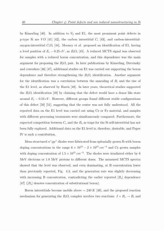
than previously reported, Fig. 4.3, and the generation rate was slightly decreasing
with increasing B concentration, contradicting the earlier reported [Bs] dependence
[47] ([Bs] denotes concentration of substitutional boron).
Boron interstitials become mobile above ∼ 240 K [48], and the proposed reaction
mechanism for generating the BiOi complex involves two reactions: I + Bs → Bi and
Chapter 4: Point defects and ion induced nanostructuring in Si 41
Figure 4.3: Generation rate of the dominating point defects as a function of dopingconcentration for epitaxial (symbols + lines) and Cz (symbols) as measured immedi-ately after proton irradiation. In addition, open symbols connected by a dashed linerepresents the results measured for the E1 level after electron irradiation in epitaxialmaterial.
42 Chapter 4: Point defects and ion induced nanostructuring in Si
Bi + Oi → BiOi, where I generated by the irradiation kicks out a boron substitu-
tional, which migrates until it encounters an oxygen interstitial. Thus, the process
can be limited by the concentrations of Bi and/or Oi. However, the measurements
can not be explained by [Oi] limiting the reaction, since oxygenated samples of the
2 × 1015 cm−3 material did not give an increased E1 concentration. In addition, a
one-to-one correlation between the loss of [Ci] and growth of [CiOi] is observed in all
the samples, indicating an abundance of oxygen. Hence, the identification of E1 as
BiOi is challenged.
Several possibilities exists to explain the [Bs] dependence of E1. Firstly, in order to
preserve the existing BiOi model, an unobservable defect level might influence the [Bs]
dependence of E1. In fact, in a recent paper by Yarykin et al. [52] it has been claimed
that BiCs, which previously has been identified as having a level at Ev + 0.29 eV , is
electrically inactive, and will form at the expence of BiOi. Secondly, as previously
reported for Cz materials, BiBs can limit the formation of BiOi. However, in Cz this
occurs for [Bs] � 2 × 1016 cm−3, but with low carbon concentrations this threshold
value may decrease. Thirdly, an alternative identification for the E1 defect must be
considered, where boron-carbon and boron-hydrogen related centers are some of the
possible alternatives. One potential candidate in this respect is BiCi since it would
have a complex formation characteristics. For a low C concentration, the generation
of Bi would dominate, and the formation of BiCi is limited by Ci, in accordance with
the present results. However, for large C concentrations compared to B, the generation
of Ci will prevail over Bi, and the formation of BiCi is limited by Bs in accordance
with Refs. [45], [46] and [47]. This is, however, very speculative and needs further
confirmation.
Chapter 4: Point defects and ion induced nanostructuring in Si 43
4.3 Defect engineering of SIMOX structures
Formation of big vacancy clusters and even cavities can be promoted by high dose
noble gas element implantation, e.g. He. It is known that a He implantation followed
by a heat treatment causes firstly the formation of He bubbles. Secondly, He atoms
diffuse out and leave behind an empty cavity with a typical size of a few nanometers [53]
[54]. Such large vacancy clusters or cavities located inside the crystal can be efficient
nucleation sites when synthesizing buried SiO2 by ion implantation. The precipitation
cites can be manipulated by for example adjusting the implantation energy.
One possible and interesting application of such precipitation, and which is explored
in Paper V, is in defect engineering of buried oxide layers for SOI manufacturing
through the SIMOX process (Separation by IMplanted OXygen) [55]. In the SIMOX
process a buried oxide layer is formed by an oxygen implantation and subsequent heat
treatment. The typical oxygen dose is large, and hence costly, and is one of the reasons
why the competing “SmartcutTM” process [56] has become the leading technology
for SOI production today. However, if one can reduce the oxygen dose necessary
for forming a complete oxide layer, SIMOX will be an interesting and competitive
alternative. To reduce the necessary oxygen dose a smaller width of the buried oxide
layer must be achieved, which is now given by the straggling of the O implantation
profile. Creating precipitation sites for oxygen growth within a narrow depth region
in the initial stage of the buried oxide formation, one can potentially enhance the
precipitation here and thus narrowing the thickness of the layer.
Furthermore, during SiO2 precipitation, Si self interstitials are known to be released
[57] and one additional measure to facilitate the SiO2 precipitates is to create extra
sinks for self interstitials, for example by dislocation loops outside of the SiO2 reaction
zone. Thus, for example a dual O and Si implantation can both supply the reaction
with oxygen, and form gettering sites for the excess interstitials.
The main functional parameter of a buried oxide (BOX) layer is its resistivity, and
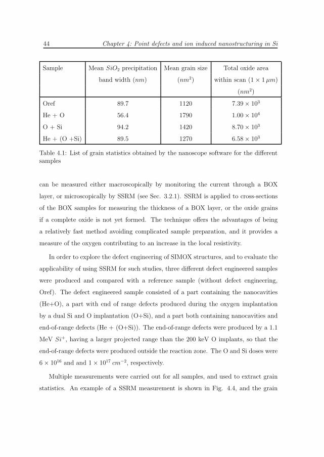
44 Chapter 4: Point defects and ion induced nanostructuring in Si
Sample Mean SiO2 precipitation Mean grain size Total oxide area
band width (nm) (nm2) within scan (1 × 1 μm)
(nm2)
Oref 89.7 1120 7.39 × 10³
He + O 56.4 1790 1.00 × 10⁴
O + Si 94.2 1420 8.70 × 10³
He + (O +Si) 89.5 1270 6.58 × 10³
Table 4.1: List of grain statistics obtained by the nanoscope software for the differentsamples
can be measured either macroscopically by monitoring the current through a BOX
layer, or microscopically by SSRM (see Sec. 3.2.1). SSRM is applied to cross-sections
of the BOX samples for measuring the thickness of a BOX layer, or the oxide grains
if a complete oxide is not yet formed. The technique offers the advantages of being
a relatively fast method avoiding complicated sample preparation, and it provides a
measure of the oxygen contributing to an increase in the local resistivity.
In order to explore the defect engineering of SIMOX structures, and to evaluate the
applicability of using SSRM for such studies, three different defect engineered samples
were produced and compared with a reference sample (without defect engineering,
Oref). The defect engineered sample consisted of a part containing the nanocavities
(He+O), a part with end of range defects produced during the oxygen implantation
by a dual Si and O implantation (O+Si), and a part both containing nanocavities and
end-of-range defects (He + (O+Si)). The end-of-range defects were produced by a 1.1
MeV Si+, having a larger projected range than the 200 keV O implants, so that the
end-of-range defects were produced outside the reaction zone. The O and Si doses were
6 × 10¹⁶ and and 1 × 1017 cm−2, respectively.
Multiple measurements were carried out for all samples, and used to extract grain
statistics. An example of a SSRM measurement is shown in Fig. 4.4, and the grain
Chapter 4: Point defects and ion induced nanostructuring in Si 45
Figure 4.4: SSRM image of a defect engineered (He + O) sample showing the oxidegrains. Increased SSRM values represent increased resistivity.
statistics are shown in Tab. 4.1. The results show that the area of the SiO2 grains de-
tected in the sample (He + O ) is larger than that of the reference sample, indicating
that the He-induced nanocavities facilitate nucleation and enhance SiO2 formation.
Moreover, the characteristic width of the precipitates is also lower for (He + O) com-
pared to Oref. The dual implantation results in a slight increase in measured total
oxide area, while the characteristic width is similar to that in the reference sample.
In conclusion, the SSRM measurements show evidence for increased precipitation
by using nanocavities in the initial stages of the oxide precipitation, while the end-
of-range defects did not improve the precipitation. However, the process needs to be
optimized and further studies are required before final conclusions can be drawn.

Chapter 5
Concluding remarks and
suggestions for future work
The major part of this thesis is devoted to the understanding of defect clustering
in heavy ion implantated Si. Firstly, progress has been made towards visualization
of the local compensation after heavy ion impacts using SPM. Secondly, the local
compensation model has been refined, decomposing the divacancy formation in V dilute2
and V dense2 components, where Fermi-level pinning mainly occurs around the secondary
collision cascades. The model explains the ion mass dependence, and the simulations
are found to be in good qualitative agreement with the experimental results. Finally,
the annealing characteristics of heavy ion impacts in Si can be consistently described
using the two mode divacancy model. However, the defect production after heavy ion
impacts is complex, and further studies are needed.
One aim with studying heavy ion impacts in impurity lean material was to monitor
the V2 migration, and thus the evolution of local compensation, through the V2O forma-
tion. Unfortunately, a hidden level around V2O(−/0), which also is observed in electron
irradiated Si, complicated the analysis, and this idea was not fully exploited in Paper
III. However, if the hiden level can be characterized or removed, the V2 migration can
be fully explored. Also in Paper III, it is expected that large vacancy clusters form after
47
48 Chapter 5: Concluding remarks and suggestions for future work
annealing at temperatures above 200◦C, and this effect requires further characteriza-
tion. In this respect, positron annihilation spectroscopy after several of the annealing
steps reported in Paper III would be very interesting, carried out after a heavy ion
bombardment such as I or Au in order to obtain a high enough defect concentration
and to maximize the average distance between each ion track. Another interesting
experiment would be to investigate heavy ion impacts using electron holography, in an
attempt to visualize the potential as illustrated in Fig. 4.1.
The work described in Paper I-III is devoted to the fundamental understanding of
heavy ion impacts in Si forming the basis of more application oriented studies. The first
step toward applications would be contact formation, and in fact, this can be realized
through a self alignment process utilizing the increased etch rate in the oxide layer
after heavy energetic ion impacts [58]. A preliminary study was made in this thesis
and Fig. 5.1 shows a topographical image of a contact formed after a Au implantation
followed by wet etching, thermal evaporation of gold and subsequent lift-off. However,
this process needs to be optimized, and in particular the contact size must be more
well controlled.
Regarding the dominant electron trap in irradiated p-type Si, Paper IV shows that
further studies on interstitial related point defects are needed, since the commonly
adopted identification of the Ec−0.25eV level as BiOi is challenged. To obtain further
insight into the behavior of the Ec − 0.25 eV level in impurity lean Si, DLTS studies
including samples with well controlled and adjustable carbon and boron concentra-
tions should be undertaken. In-situ DLTS measurements of the Bi to Ec − 0.25 eV
transformation and a possible correlation with Ci should also be pursued.
Paper V shows that defect engineering has a potential for improving existing Si
processes, for example in the formation of buried oxide layers through the SIMOX
process. By forming nanosized vacancy clusters oxide nucleation can be enhanced,
potentially reducing the required oxygen dose during the SIMOX process. However, the
width of the BOX layer, and thus the precipitation, is very sensitive to the position of
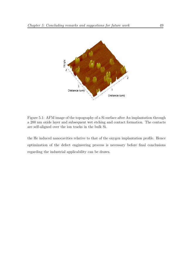
Chapter 5: Concluding remarks and suggestions for future work 49
Figure 5.1: AFM image of the topography of a Si surface after Au implantation througha 200 nm oxide layer and subsequent wet etching and contact formation. The contactsare self-aligned over the ion tracks in the bulk Si.
the He induced nanocavities relative to that of the oxygen implantation profile. Hence
optimization of the defect engineering process is necessary before final conclusions
regarding the industrial applicability can be drawn.


Bibliography
[1] J.W. Corbett and G.D. Watkins Phys. Rev. Lett., vol. 7, p. 314, 1961.
[2] S.M. Sze, Physics of Semiconductor Devices. John Wiley & Sons, 2nd ed., 1981.
[3] B.G. Streetman and S. Banerjee, Solid State Electronic Devices. Prentice Hall,5th ed., 2000.
[4] C. Lombardi, S. Manzini, and A. Saporito IEEE Transactions on computer-aided
design of integrated circuits and systems, vol. 7, no. 11, p. 1164, 1988.
[5] G. Masetti, M. Severi, and S. Solmi IEEE Transactions on electron devices, vol. 30,no. 7, p. 764, 1983.
[6] Synopsys, Inc., Sentaurus Device, x-2005.10 ed., 2005.
[7] S.A. Campbell, The Science and Engineering of Microelectronic Fabrication. Ox-ford University Press, 2001.
[8] B.G. Svensson, C. Jagadish, A. Hallen, and J. Lalita Phys. Rev. B, vol. 55,p. 10498, 1997.
[9] W. Shockley and W.T. Read Phys. Rev., vol. 87, p. 835, 1952.
[10] R.N. Hall Phys. Rev., vol. 87, p. 387, 1952.
[11] P. Blood and J.W. Orton, The Electrical Characterization of Semiconductors:
Majority Carriers and Electron States. Academic Press, 1992.
[12] D.V. Lang J. Appl. Phys., vol. 45, p. 3014, 1974.
[13] G. Binning, H. Rohrer, C. Gerber, and E. Weibel Phys. Rev. Lett., no. 49, p. 57,1982.
[14] G. Binnig, C.F. Quate, and C. Gerber Phys. Rev. Lett., vol. 56, p. 930, 1986.
[15] C.C. Williams, J. Slinkman, W.P. Hough, and H.K. Wickramasinghe Appl. Phys.
Lett., vol. 55, no. 16, p. 1662, 1989.
51
52 Bibliography
[16] C.C. Williams Annu. Rev. Mater. Sci., vol. 29, p. 471, 1999.
[17] P. D. J. Snauwaert, T. Clarysse, W. Vandervorst, and L. Hellemans Appl. Phys.
Lett., vol. 66, p. 1530, 1995.
[18] R. Holm, Electrical Contacts, Theory and Applications. Springer, 4th ed., 1967.
[19] P. Eyben, Scanning spreading resistance microscopy: High resolution two-
dimensional carrier profiling of semiconductor structures. PhD thesis, KatholiekeUniversiteit Leuven, 2004.
[20] Veeco Application Module: Dimension and Multimode Manual, Software Version5.12 r4, Rev D.
[21] J.J. Kopanski, J.F. Marchiando, and J.R. Lowney J. Vac. Sci Technol. B, vol. 14,p. 242, 1996.
[22] F. Giannazzo, V. Raineri, S. Mirabella, E. Bruno, G. Impellizzeri, and F. PrioloMat. Sci. Eng. B, vol. 124, p. 54, 2005.
[23] F. Giannazzo, V. Raineri, S. Mirabella, G. Impellizzeri, F. Priolo, M. Fedele, andR. Mucciato J. Vac. Sci. Technol. B, vol. 24, no. 1, p. 370, 2006.
[24] J.F. Ziegler, J.P. Biersack, and U. Littmark, The stopping and Range of Ions in
Solids. New York: Pergamon, 1985.
[25] B.G. Svensson and J.L. Lindstrom J. Appl. Phys., vol. 72, p. 5616, 1992.
[26] A. O. Evwaraye and E. Sun J. Appl. Phys., vol. 47, no. 9, p. 3776, 1976.
[27] A. Hallen, B.U.R. Sundquist, Z. Paska, B.G. Svensson, M. Rosling, and J. TirenJ. Appl. Phys., vol. 67, p. 1266, 1990.
[28] B.G. Svensson, B. Mohadjeri, A. Hallen, J.H. Svensson, and J.W. Corbett Phys.
Rev. B, vol. 43, p. 2292, 1991.
[29] R.M. Fleming, C.H. Seager, D.V. Lang, P.J. Cooper, E. Bielejec, andJ.M.Campbell J. Appl. Phys., vol. 102, p. 043711, 2007.
[30] N. Abdelgader and J.H. Evans-Freeman J. Appl. Phys., vol. 93, p. 5118, 2003.
[31] N. Keskitalo, A. Hallen, J. Lalita, and B.G. Svensson Mat. Res. Soc. Symp. Proc.,vol. 469, p. 233, 1997.
[32] E.V. Monakhov, J. Wong-Leung, A.Yu. Kuznetsov, C. Jagadish, and B.G. Svens-son Phys. Rev. B, vol. 65, p. 245201, 2002.

Bibliography 53
[33] L. Vines, E.V. Monakhov, B.G. Svensson, J. Jensen, A. Hallen, and A. Yu.Kuznetsov Phys. Rev. B, vol. 73, p. 085312, 2006.
[34] Synopsys Inc., 700 East Middlefield Road, Mountain View, CA 94043, USA; seealso http://www.synopsys.com/.
[35] P. Pellegrino, P. Leveque, J. Lalita, A. Hallen, C. Jagadish, and B.G. SvenssonPhys. Rev. B, vol. 64, p. 195211, 2001.
[36] E.V. Monakhov, A. Ulyashin, G. Alfieri, A.Yu. Kuznetsov, B.S. Avset, and B.G.Svensson Phys. Rev. B, vol. 69, p. 153202, 2004.
[37] A. Kawasuso, M. Hasegawa, M. Suezawa, S. Yamaguchi, and K. Sumino Appl.
Surf. Sci., vol. 85, p. 280, 1995.
[38] M. Mikelsen, E.V. Monakhov, G. Alfieri, B.S. Avset, and B.G. Svensson Phys.
Rev. B, vol. 72, p. 195207, 2005.
[39] A. Hallen, N. Keskitalo, F. Masszi, and V. Nagl J. Appl. Phys., vol. 79, no. 8,p. 3906, 1996.
[40] L.C. Kimerling IEEE Trans. Nucl. Sci., vol. 23, p. 1497, 1976.
[41] G. Bemski J. Appl. Phys, vol. 30, p. 1195, 1959.
[42] G.D. Watkins, J.W. Corbett, and R.M. Walker J. Appl. Phys., vol. 30, p. 1198,1959.
[43] A.R. Bean and R.C. Newman Solid State Commun., vol. 8, p. 175, 1970.
[44] L.J. Cheng and P. Vajda J. Appl. Phys., vol. 40, p. 4679, 1969.
[45] P.M. Mooney, L.J. Cheng, M. Suli, J.D. Gerson, and J.W. Corbett Phys. Rev. B,vol. 15, p. 3836, 1977.
[46] P.J. Drevinsky, C.E. Caefer, S.P. Tobin, J.C. Mikkelsen, and L.C. KimerlingMater. Res. Soc. Symp. Proc., vol. 104, p. 167, 1988.
[47] L.C. Kimerling, M.T. Asom, J.L. Benton, P.J. Drevinsky, and C.E. Caefer Mater.
Sci. Forum, vol. 38-41, 1989.
[48] R.D. Harris, J.L. Newton, and G.D. Watkins Phys. Rev. B, vol. 36, p. 1094, 1987.
[49] J. Adey, R. Jones, and P.R. Briddon Appl. Phys. Lett, vol. 83, no. 4, p. 665, 2003.
[50] M. Sanati and S.K. Estreicher Phys. Rev. B, vol. 72, p. 165206, 2005.
54 Bibliography
[51] A. Carvalho, R. Jones, M. Sanati, S.K. Estreicher, J. Coutinho, and P.R. BriddonPhys. Rev. B, vol. 73, p. 245210, 2006.
[52] N. Yarykin, O.V. Feklisova, and J. Weber Phys. Rev. B, vol. 69, p. 045201, 2004.
[53] C.C. Griffioen, J.H. Evans, P.C. De Jong, and A. Van Veen Nucl. Instrum. Meth-
ods. Phys. Res. B, vol. 27, p. 417, 1987.
[54] W. Fukarek and J.R. Kaschny J. Appl. Phys., vol. 86, p. 4160, 1999.
[55] R. Kogler, A. Mucklich, J.R. Kaschny, H. Reuther, F. Eichhorn, H. Hutter, andW. Skorupa Solid State Phenom., vol. 108-109, p. 321, 2005.
[56] M. Bruel Electronics Lett., vol. 31, no. 14, p. 1201, 1995.
[57] S.M. Hu J. Appl. Phys., vol. 45, no. 4, p. 1567, 1974.
[58] J. Jensen, A. Razpet, M. Skupinski, and G. Possnert Nucl. Instr. Methods Phys.
Res. B, vol. 245, no. 1, p. 269, 2006.