Embed Size (px)
Citation preview
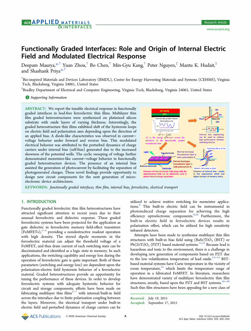
Functionally Graded Interfaces: Role and Origin of Internal ElectricField and Modulated Electrical ResponseDeepam Maurya,*,† Yuan Zhou,† Bo Chen,† Min-Gyu Kang,† Peter Nguyen,‡ Mantu K. Hudait,‡
and Shashank Priya*,†
†Bio-inspired Materials and Devices Laboratory (BMDL), Center for Energy Harvesting Materials and Systems (CEHMS), VirginiaTech, Blacksburg, Virginia 24061, United States‡Bradley Department of Electrical and Computer Engineering, Virginia Tech, Blacksburg, Virginia 24061, United States
*S Supporting Information
ABSTRACT: We report the tunable electrical response in functionallygraded interfaces in lead-free ferroelectric thin films. Multilayer thinfilm graded heterostructures were synthesized on platinized siliconsubstrate with oxide layers of varying thickness. Interestingly, thegraded heterostructure thin films exhibited shift of the hysteresis loopson electric field and polarization axes depending upon the direction ofan applied bias. A diode-like characteristics was observed in current−voltage behavior under forward and reverse bias. This modulatedelectrical behavior was attributed to the perturbed dynamics of chargecarriers under internal bias (self-bias) generated due to the increasedskewness of the potential wells. The cyclic sweeping of voltage furtherdemonstrated memristor-like current−voltage behavior in functionallygraded heterostructure devices. The presence of an internal biasassisted the generation of photocurrent by facilitating the separation ofphotogenerated charges. These novel findings provide opportunity todesign new circuit components for the next generation of micro-electronic device architectures.
KEYWORDS: functionally graded interfaces, thin film, internal bias, ferroelectric, electrical transport
1. INTRODUCTION
Functionally graded ferrolectric thin film heterostructures haveattracted significant attention in recent years due to theirunusual ferroelectric and dielectric response. These gradedferroelectric systems have been projected for the application asgate dielectric in ferroelectric memory field-effect transistors(FeMFETs),1−4 providing a nondestructive readout operationwith high density. The stored dipole moments in theferroelectric material can adjust the threshold voltage of aFeMFET, and thus drain current of each switching state can bediscriminated and identified as a logic state in memory. In suchapplications, the switching capability and energy loss during theoperation of ferroelectric gate is quite important. Both of theseparameters (switching and energy loss) are dependent upon thepolarization-electric field hysteresis behavior of a ferroelectricmaterial. Graded heterostructures provide an opportunity fortuning the performance of these devices. In order to developferroelectric systems with adequate hysteretic behavior forcircuit and storage components, efforts have been made onfabricating multilayer thin films5−7 with internal/built-in fieldacross the interaface due to finite polarization coupling betweenthe layers. Moreover, the electrical transport under built-inelectric field and perturbed dynamics of charge carriers can be
utilized to achieve resitive switching for memrister applica-tions.8 This built-in electric field can be instrumental inphotoinduced charge separation for achieving the highefficiency optoelectronic components.9,10 Furthermore, thebuilt-in electric field in ferroelectric devices results inpolarization offset, which can be utilized for high sensitivityinfrared detectors.Attempts have been made to synthesize multilayer thin film
structures with built-in bias field using (BaSr)TiO3 (BST) orPb(ZrTi)O3 (PZT) based material systems.11,12 Because lead ishazardous and toxic to the environment, there is a challenge indeveloping new generation of components based on PZT dueto the low volatilization temperature of lead oxide.13−15 BST-based material systems have Curie temperature in the vicinity ofroom temperature,12 which limits the temperature range ofoperation in a fabricated FeMFET. In literature, researchershave demonstrated variety of multilayer ferroelectric thin filmstructures, mostly, based upon the PZT and BST systems.16−20
Such thin film structures have been appealing for a new class of
Received: July 19, 2015Accepted: September 17, 2015
Research Article
www.acsami.org
© XXXX American Chemical Society A DOI: 10.1021/acsami.5b06544ACS Appl. Mater. Interfaces XXXX, XXX, XXX−XXX
transcapacitive ferroelectric devices, which are viewed to be thedielectric equivalent of the semiconductor junction devices.11,21
However, they require a new material system and architectureto overcome the challenges imposed by environment, temper-ature range, ferroelectric hysteresis and current−voltagebehavior. Here, a systematic investigation is presented onnew lead-free graded heterostructures, which can overcomeabove challenges and provide an opportunity to developpractical components.We have synthesized functionally graded interfaces in the
lead-free thin films of BaTiO3 (BT) and 0.975BaTiO3−0.025Ba(Cu1/2Nb2/3)O3 (BT−BCN) and successfully demon-strated the modulation of ferroelectric behavior and electricalresponse in such structures. The design of lead-free piezo-electric/ferroelectric BT−BCN with superier functionalresponse has been discussed elsewhere.22 Briefly, severalcompositions were synthesized over a wide compositionalrange and characterized. The composition 0.975BaTiO3−0.025Ba(Cu1/2Nb2/3)O3 was found to exhibit superior piezo-electric response with d33 ∼ 330 pC/N and kp ∼ 46%.22 Thepiezoelectric response of BT−BCN was comparable to that ofcommercial lead-based PZT (Pz23, Ferroperm) with d33 = 330pC/N and kp = 0.52. Moreover, BT−BCN had a tetragonalcrystal structure similar to that of BaTiO3. The differences intetragonality and polarization of various ferroelectric layersresulted in strain and polarization gradient across the thicknessof thin film that induced the translation of the P−E hysteresisloop on E-field and polarization axes, diode-like current−voltage (I−V) behavior, and asymmetry in capacitance−voltage(C−V) plots. The J−V characteristics (J represents the currentdensity) exhibited high rectification ratio for graded hetero-structure. The functionally graded interfaces in the thin filmarchitectures further exhibited memristor-like resistive switch-ing behavior. Interestingly, the photovoltaic effect was observedin the specimen having functionally graded interfaces withinternal electric field. Here, we provide a fundamentalunderstanding of the modulated electrical response and therole of internal electric fields in imparting these desiredcharacteristics to the functionally graded ferroelectric hetero-structures.
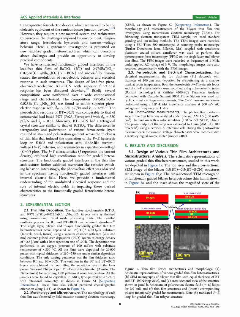
2. EXPERIMENTAL SECTION2.1. Thin Film Deposition. The lead-free stoichiometric BaTiO3
and 0.975BaTiO3−0.025Ba(Cu1/3Nb2/3)O3 targets were synthesizedusing conventional mixed oxide processing route. The detailedsynthesis process for BT and BT−BCN can be found elsewhere.23
The single layer, bilayer, and trilayer functionally graded thin filmheterostructures were deposited on Pt(111)/Ti/SiO2/Si substrate(Inostek, Seoul, Korea) using a vacuum chamber with KrF (λ = 248nm) excimer pulsed laser deposition (PLD) system at energy densityof ∼2.5 J/cm2 with a laser repetition rate of 10 Hz. The deposition wasperformed in an oxygen pressure of 100 mTorr with substratetemperature of ∼800 °C. All the films were deposited for 20 000pulses with typical thickness of 250−280 nm under similar depositionconditions. The only varying parameter was the film thickness ratiobetween BT and BT−BCN. The variation in the BT and BT−BCNlayers was achieved by controlling the repetition rate of the laserpulses. We used Philips X’pert Pro X-ray diffractometer (Almelo, TheNetherlands) for recording XRD patterns at room temperature. All thesamples were found to crystallize in ABO3 type perovskite structurewith tetragonal symmetry, as shown in Figure S1 (SupportingInformation). These films also exhibit preferred crystallographicorienation along ⟨111⟩, as shown in Figure S1.2.2. Morphology and Microstructure. The morphology of each
thin film was observed by field emission scanning electron microscopy
(SEM), as shown in Figure S2 (Supporting Information). Themorphology and microstructure of the bilayer thin film wasinvestigated using transmission electron microscopy (TEM). Forfabricating electron transparent TEM sample, we used standardgrinding and ion-milling methods. The TEM images were recordedusing a FEI Titan 300 microscope. A scanning probe microscope(Bruker Dimension Icon, Billerica, MA) coupled with conductiveplatinum coated silicon cantilever was used to perform thepiezoresponse force microscopy (PFM) on the single layer and bilayerthin films. The PFM images were recorded at frequency of 1 MHzunder applied AC voltage of 3 V. The morphology images were alsorecorded concomitantly with the PFM images.
2.3. Ferroelectric and Electrical Characterization. Forelectrical measurements, the top platinum (Pt) electrode withdiameter of 500 μm was deposited by rf-sputtering via a shadowmask at room temperature. Both the ferroelectric P−E hysteresis loopsand the I−V characteristics were recorded using a ferroelectric tester(Radiant technology). A Keithley 4200-SCS Parameter Analyzerconnected with Cascade Summit 9000 Probe Station was used forcyclic current - voltage measurements. The C−V measurements wereperformed using a HP 4194A impedance analyzer at 500 mV ACvoltage and frequency of 1 kHz.
2.4. Photovoltaic Measurements. The photovoltaic perform-ance of the thin films was analyzed under one sun AM 1.5 (100 mW/cm2) illumination with a solar simulator (150 W Sol 2ATM, Oriel).The power output of the lamp was calibrated to 1 Sun (AM1.5G, 100mW/cm2) using a certified Si reference cell. During the photovoltaicmeasurements, the current−voltage characteristics were recorded witha Keithley digital source meter (model 2400).
3. RESULTS AND DISCUSSION
3.1. Design of Various Thin Film Architectures andMicrostructural Analysis. The schematic representations ofvarious graded thin film heterostructures, studied in this work,are depicted in Figure 1a. The top view and the cross-sectionalSEM image of the bilayer 0.5(BT)−0.5(BT−BCN) structuresare shown in Figure 1b,c. The cross-sectional TEM micrographof functionally graded bilayer heterostructure thin film is shownin Figure 2a, and the inset shows the magnified view of the
Figure 1. Thin film device architectures and morphology. (a)Schematic representation of various graded thin film heterostructures,(b) SEM micrographs of bilayer thin film with equal thickness of BTand BT−BCN (top view), and (c) cross-sectional view of the structureshown in panel b. Schematic of polarization electric field (P−E) loopsfor (e) bulk and (f) thin film structures and (insets) correspondingtrilayer functionally graded heterostructures. Note the translated P−Eloop for graded thin film trilayer structure.
ACS Applied Materials & Interfaces Research Article
DOI: 10.1021/acsami.5b06544ACS Appl. Mater. Interfaces XXXX, XXX, XXX−XXX
B
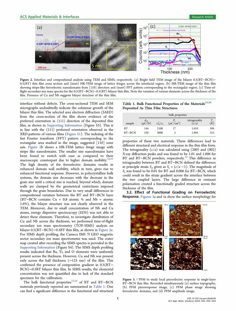
interface without defects. The cross-sectional TEM and SEMmicrographs undoubtedly indicate the columnar growth of thebilayer thin film. The selected area electron diffraction (SAED)from the cross-section of the film shows evidence of thepreferred orientation in ⟨111⟩ direction of the deposited thinfilm, as shown in Supporting Information (Figure S3). This isin line with the ⟨111⟩ preferred orientation observed in theXRD-patterns of various films (Figure S1). The indexing of thefast Fourier transform (FFT) pattern corresponding to therectangular area marked in the image, suggested [110] zoneaxis. Figure 2b shows a HR-TEM lattice fringe image withstripe like nanodomains. The smaller size nanodomains havebeen found to switch with ease as compared to theirmacroscopic counterpart due to higher domain mobility.24,25
The high density of the ferroelectric domains results inenhanced domain wall mobility, which in turn, gives rise toenhanced functional response. However, in polycrystalline bulksystems, the domain size decreases with the decrease in thegrain size until a critical size is reached, beyond which, domainwalls are clamped by the geometrical restrictions imposedthrough the grain boundaries. Due to very small differences incompositional variation between the BT and BT−BCN layer(BT−BCN contains Cu = 0.8 atomic % and Nb = atomic1.6%), the bilayer structure was not clearly observed in theTEM. Moreover, due to small concentration of Nb and Cuatoms, energy dispersive spectroscopy (EDS) was not able todetect these elements. Therefore, to investigate distribution ofCu and Nb across the thickness, we performed time-of-flightsecondary ion mass spectrometry (TOF-SIMS) analysis onbilayer 0.5(BT−BCN)−0.5BT thin film, as shown in Figure 2c.For SIMS depth profiling, the Cameca IMS 7f GEO magneticsector secondary ion mass spectrometer was used. The cratermap created after recording the SIMS spectra is provided in theSupporting Information (Figure S4). The SIMS depth profilingresults indicated that Ba, Ti, and O elements were uniformlypresent across the thickness. However, Cu and Nb was presentonly across the half thickness (∼125 nm) of the film. Thisconfirmed the presence of composition gradient in 0.5(BT−BCN)−0.5BT bilayer thin film. In SIMS results, the elementalconcentration was not quantified due to lack of the standardspecimen for the calibration.The bulk functional properties23,26 of BT and BT−BCN
materials previously reported are summarized in Table 1. Onecan find a significant difference in the functional and structural
properties of these two materials. These differences lead todifferent structural and electrical response in the thin film form.The tetragonality (c/a) was calculated using (200) and (002)X-ray diffraction peaks and was found to be 1.01 and 1.006 forBT and BT−BCN powders, respectively.23 This difference intetragonality between BT and BT−BCN defined the differencein principle strain Ss, given as Ss = (c/a −1). The magnitude ofSs was found to be 0.01 for BT and 0.006 for BT−BCN, whichcould result in the strain gradient across the interface betweenthe two coupled layers. The large difference in remnantpolarization created a functionally graded structure across thethickness of the film.
3.2. Effect of Functional Grading on FerroelectricResponse. Figures 3a and 4a show the surface morphology for
Figure 2. Interface and compositional analysis using TEM and SIMS, respectively. (a) Bright field TEM image of the bilayer 0.5(BT−BCN)−0.5(BT) thin film cross section and (inset) HR-TEM image of lattice fringes across the interfacial region. (b) HR-TEM image of the thin filmshowing stripe-like ferroelectric nanodomains from [110] direction and (inset) FFT pattern corresponding to the rectangular region. (c) Time-of-flight secondary-ion mass spectra for the 0.5(BT−BCN)−0.5(BT) bilayer thin film. Note the variation of various elements across the thickness of thefilm. Presence of Cu and Nb suggests bilayer structure of the thin film.
Table 1. Bulk Functional Properties of the Materials23,26
Deposited As Thin Film Structures
bulk properties
sampled33
(pC/N) ε33T /εo
Pr(μC/cm2)
tetragonality(c/a)
Tc(K)
BT 144 2100 17 1.010 398BT−BCN 330 3000 5 1.004 353
Figure 3. | PFM to study local piezoelectric response in single-layerBT−BCN thin film. Recorded simultaneously (a) surface topography,(b) PFM piezoresponse image, (c) PFM phase image showingferroelectric domains, and (d) PFM amplitude image.
ACS Applied Materials & Interfaces Research Article
DOI: 10.1021/acsami.5b06544ACS Appl. Mater. Interfaces XXXX, XXX, XXX−XXX
C
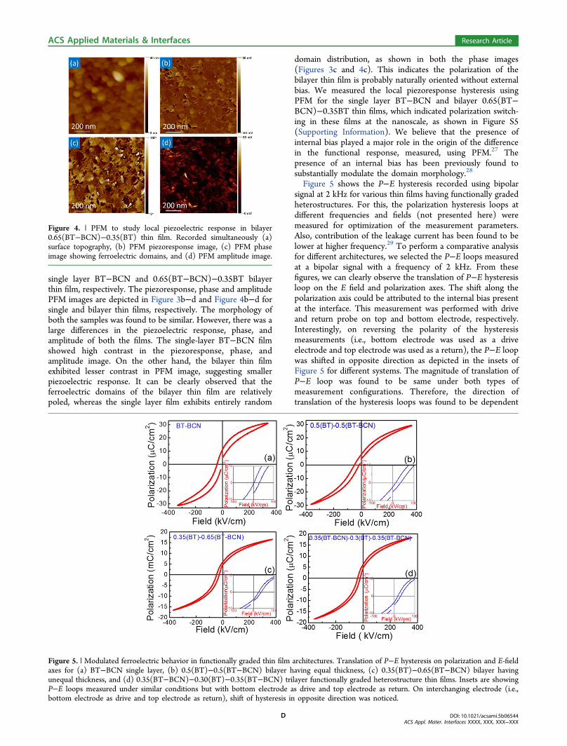
single layer BT−BCN and 0.65(BT−BCN)−0.35BT bilayerthin film, respectively. The piezoresponse, phase and amplitudePFM images are depicted in Figure 3b−d and Figure 4b−d forsingle and bilayer thin films, respectively. The morphology ofboth the samples was found to be similar. However, there was alarge differences in the piezoelectric response, phase, andamplitude of both the films. The single-layer BT−BCN filmshowed high contrast in the piezoresponse, phase, andamplitude image. On the other hand, the bilayer thin filmexhibited lesser contrast in PFM image, suggesting smallerpiezoelectric response. It can be clearly observed that theferroelectric domains of the bilayer thin film are relativelypoled, whereas the single layer film exhibits entirely random
domain distribution, as shown in both the phase images(Figures 3c and 4c). This indicates the polarization of thebilayer thin film is probably naturally oriented without externalbias. We measured the local piezoresponse hysteresis usingPFM for the single layer BT−BCN and bilayer 0.65(BT−BCN)−0.35BT thin films, which indicated polarization switch-ing in these films at the nanoscale, as shown in Figure S5(Supporting Information). We believe that the presence ofinternal bias played a major role in the origin of the differencein the functional response, measured, using PFM.27 Thepresence of an internal bias has been previously found tosubstantially modulate the domain morphology.28
Figure 5 shows the P−E hysteresis recorded using bipolarsignal at 2 kHz for various thin films having functionally gradedheterostructures. For this, the polarization hysteresis loops atdifferent frequencies and fields (not presented here) weremeasured for optimization of the measurement parameters.Also, contribution of the leakage current has been found to belower at higher frequency.29 To perform a comparative analysisfor different architectures, we selected the P−E loops measuredat a bipolar signal with a frequency of 2 kHz. From thesefigures, we can clearly observe the translation of P−E hysteresisloop on the E field and polarization axes. The shift along thepolarization axis could be attributed to the internal bias presentat the interface. This measurement was performed with driveand return probe on top and bottom electrode, respectively.Interestingly, on reversing the polarity of the hysteresismeasurements (i.e., bottom electrode was used as a driveelectrode and top electrode was used as a return), the P−E loopwas shifted in opposite direction as depicted in the insets ofFigure 5 for different systems. The magnitude of translation ofP−E loop was found to be same under both types ofmeasurement configurations. Therefore, the direction oftranslation of the hysteresis loops was found to be dependent
Figure 4. | PFM to study local piezoelectric response in bilayer0.65(BT−BCN)−0.35(BT) thin film. Recorded simultaneously (a)surface topography, (b) PFM piezoresponse image, (c) PFM phaseimage showing ferroelectric domains, and (d) PFM amplitude image.
Figure 5. | Modulated ferroelectric behavior in functionally graded thin film architectures. Translation of P−E hysteresis on polarization and E-fieldaxes for (a) BT−BCN single layer, (b) 0.5(BT)−0.5(BT−BCN) bilayer having equal thickness, (c) 0.35(BT)−0.65(BT−BCN) bilayer havingunequal thickness, and (d) 0.35(BT−BCN)−0.30(BT)−0.35(BT−BCN) trilayer functionally graded heterostructure thin films. Insets are showingP−E loops measured under similar conditions but with bottom electrode as drive and top electrode as return. On interchanging electrode (i.e.,bottom electrode as drive and top electrode as return), shift of hysteresis in opposite direction was noticed.
ACS Applied Materials & Interfaces Research Article
DOI: 10.1021/acsami.5b06544ACS Appl. Mater. Interfaces XXXX, XXX, XXX−XXX
D
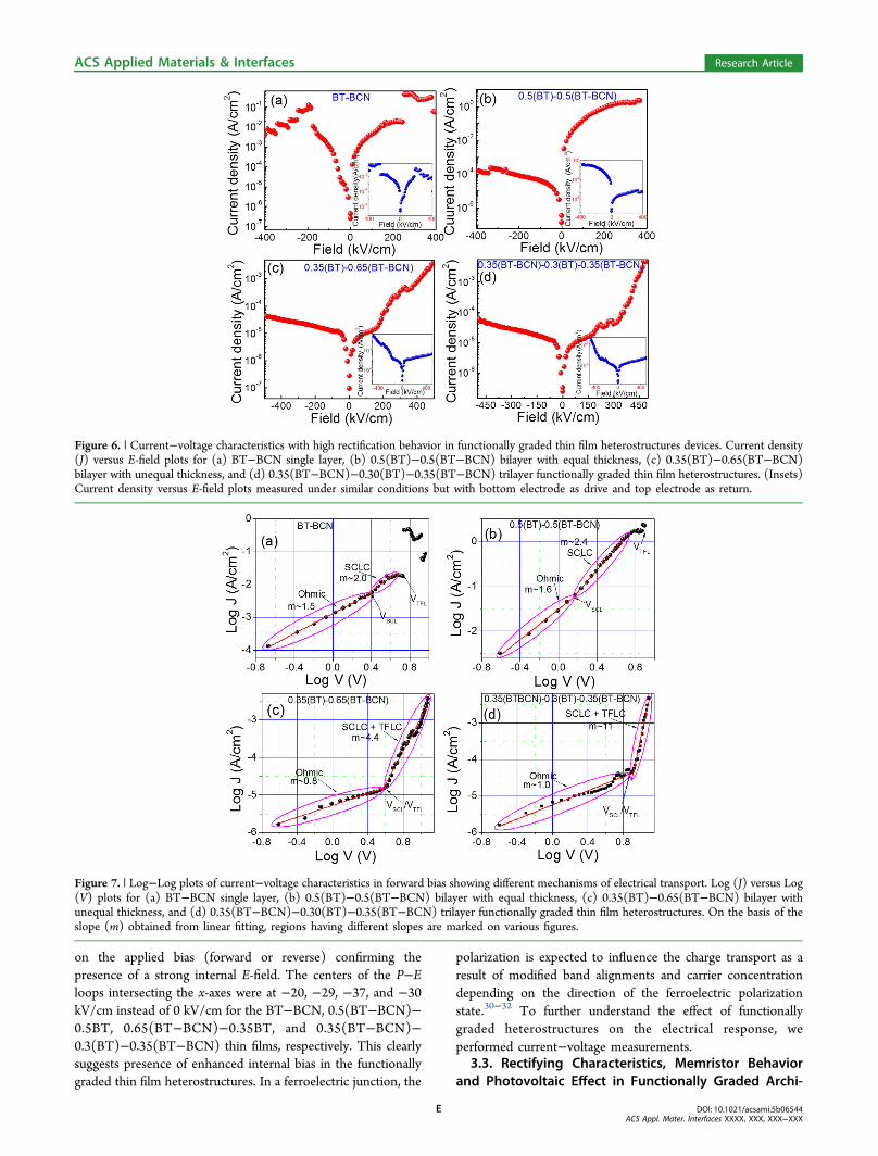
on the applied bias (forward or reverse) confirming thepresence of a strong internal E-field. The centers of the P−Eloops intersecting the x-axes were at −20, −29, −37, and −30kV/cm instead of 0 kV/cm for the BT−BCN, 0.5(BT−BCN)−0.5BT, 0.65(BT−BCN)−0.35BT, and 0.35(BT−BCN)−0.3(BT)−0.35(BT−BCN) thin films, respectively. This clearlysuggests presence of enhanced internal bias in the functionallygraded thin film heterostructures. In a ferroelectric junction, the
polarization is expected to influence the charge transport as aresult of modified band alignments and carrier concentrationdepending on the direction of the ferroelectric polarizationstate.30−32 To further understand the effect of functionallygraded heterostructures on the electrical response, weperformed current−voltage measurements.
3.3. Rectifying Characteristics, Memristor Behaviorand Photovoltaic Effect in Functionally Graded Archi-
Figure 6. | Current−voltage characteristics with high rectification behavior in functionally graded thin film heterostructures devices. Current density(J) versus E-field plots for (a) BT−BCN single layer, (b) 0.5(BT)−0.5(BT−BCN) bilayer with equal thickness, (c) 0.35(BT)−0.65(BT−BCN)bilayer with unequal thickness, and (d) 0.35(BT−BCN)−0.30(BT)−0.35(BT−BCN) trilayer functionally graded thin film heterostructures. (Insets)Current density versus E-field plots measured under similar conditions but with bottom electrode as drive and top electrode as return.
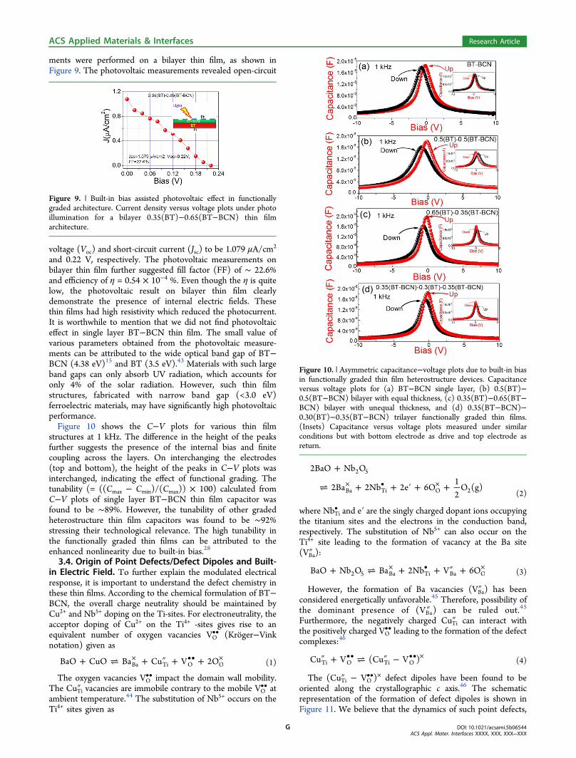
Figure 7. | Log−Log plots of current−voltage characteristics in forward bias showing different mechanisms of electrical transport. Log (J) versus Log(V) plots for (a) BT−BCN single layer, (b) 0.5(BT)−0.5(BT−BCN) bilayer with equal thickness, (c) 0.35(BT)−0.65(BT−BCN) bilayer withunequal thickness, and (d) 0.35(BT−BCN)−0.30(BT)−0.35(BT−BCN) trilayer functionally graded thin film heterostructures. On the basis of theslope (m) obtained from linear fitting, regions having different slopes are marked on various figures.
ACS Applied Materials & Interfaces Research Article
DOI: 10.1021/acsami.5b06544ACS Appl. Mater. Interfaces XXXX, XXX, XXX−XXX
E
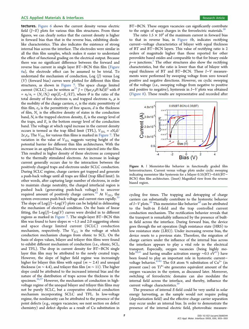
tectures. Figure 6 shows the current density versus electricfield (J−E) plots for various thin film structures. From thesefigures, we can clearly notice that the current density is higherin forward bias than that in the reverse bias, exhibiting diode-like characteristics. This also indicates the existence of stronginternal bias across the interface. The electrodes were similar inall the thin film samples, which makes it easier to understandthe effect of functional grading on the electrical output. Becausethere was no significant difference between the forward andreverse bias current in single layer BT−BCN thin film (Figure6a), the electrode effect can be assumed to be trivial. Tounderstand the mechanism of conduction, Log (J) versus Log(V) (forward bias) curves were plotted for different thin filmsstructures, as shown in Figure 7. The space charge limitedcurrent (SCLC) can be written as33 J = (9μεsε0θ/8d)E
2 with θ= nf/nt = (Nc/Nt) exp(Et−Ec/kT), where θ is the ratio of thetotal density of free electrons nf and trapped electrons nt, μ isthe mobility of the charge carriers, εs is the static permittivity ofthin film, ε0 is the permittivity of free spaces, d is the thicknessof film, Nc is the effective density of states in the conductionband, Nt is the trapped electron density, Et is the energy level ofthe traps, and Ec is the bottom energy level of the conductionband. The voltage at which rapid increase in the current densityoccurs is termed as the trap filled limit (TFL), VTFL = eNtd/2εsε0. The VTFL for various thin films is marked in Figure 7. Thevariation in the value of VTFL suggests varying height of thepotential barrier for different thin film architectures. With theincrease in an applied bias, electrons were injected into the film.This resulted in higher density of these electrons as comparedto the thermally stimulated electrons. An increase in leakagecurrent generally occurs due to the interaction between thepositively charged traps and electrons under SCLC conduction.During SCLC regime, charge carriers get trapped and generatea push-back voltage until all traps are filled (trap filled limit). Inother words, after capturing large number of electrons, in orderto maintain charge neutrality, the charged interfacial region ispushed back (generating push-back voltage) to uncoverrequired amount of positively charge carriers.34 At VTFL, thesystem overcomes push-back voltage and current rises rapidly.35
The slope of Log(J)−Log(V) plots can be helpful in delineatingthe mechanism of electrical condition. On the basis of linearfitting, the Log(J)−Log(V) curves were divided in to differentregions as marked in Figure 7. The single-layer BT−BCN thinfilm was found to have slopes m ∼1.5 and 2.0 suggesting ohmicand space charge limited current (SCLC) conductionmechanism, respectively. The VSCL is the voltage at whichconduction mechanism changes from ohmic to SCL. On thebasis of slopes values, bilayer and trilayer thin films were foundto exhibit different mechanism of conduction (i.e., ohmic, SCL,and TFL). The drop in current density for BT−BCN singlelayer thin film may be attributed to the newly created traps.However, the slope of higher field regime was increasinglyhigher for bilayer thin films with equal (m ∼ 2.4) and unequalthickness (m ∼ 4.4), and trilayer thin film (m ∼ 11). The higherslope could be attributed to the increased internal bias and thenature of the distribution of traps across the thickness in thespecimen.36,37 However, the mechanism of conduction in high-voltage regime of the unequal bilayer and trilayer thin films maynot be purely SCLC, but a cooperative electrical conductionmechanism incorporating SCLC and TFL. In low-voltageregime, the nonlinearity can be attributed to the presence of thepoint defects (e.g., oxygen vacancies; see next section on defectchemistry) and defect dipoles as a result of Cu substitution in
BT−BCN. These oxygen vacancies can significantly contributeto the origin of space charges in the ferroelectric materials.38
The ratio 1.5 × 10⁴ of the maximum current in forward biasto that in reverse bias, in Figure 6b, indicates rectifyingcurrent−voltage characteristics of bilayer with equal thicknessof BT and BT−BCN layers. This value of rectifying ratio is 2orders of magnitude higher than those reported for otherperovskite based oxides and comparable to that for binary oxidep−n junctions.1 The other structures also show the rectifyingcharacteristics, but the ratio is lower than that of bilayer withequal thickness of BT and BT−BCN. These I−V measure-ments were performed by sweeping voltage from zero towardpositive and negative directions. However, on cyclic sweepingof the voltage (i.e., sweeping voltage from negative to positiveand positive to negative), hysteresis in I−V plots was obtained(Figure 8). These results are representative and recorded after
cycling five times. The trapping and detrapping of chargecarriers can substantially contribute to the hysteretic behaviorof I−V plots.39 This memristor-like behavior40 can be attributedto the built-in E-field and the trap controlled currentconduction mechanism. The rectification behavior reveals thatthe transport is remarkably influenced by the presence of built-in field across the interface. During forward bias, the devicegoes through the set operation (high resistance state (HRS) tolow resistance state (LRS)). Under increasing reverse bias, thedevice resets to a previous state. Therefore, the migration ofcharge carriers under the influence of the internal bias acrossthe interfaces appears to play a vital role in the electricaltransport. Especially, oxygen vacancies (being highly mo-bile38,41 and having smaller activation energy ∼0.5 eV41) havebeen found to play an important role in hysteretic current−voltage behavior.4142 The 0.8 atom % substitution of Cu2+ (inpresent case) on Ti4+-site generates equivalent amount of theoxygen vacancies in the system, as discussed later. Moreover,switching of ferroelectric domains can also modulate theinternal field across the interface, and thereby, influence thecurrent voltage characteristics.39
The presence of internal E-field could be very useful in solarenergy harvesting, as the sample would not require poling(depolarization field) and the effective charge carrier separationmay occur under an internal bias. In order to demonstrate thepresence of the internal electric field, photovoltaic measure-
Figure 8. | Memristor-like behavior in functionally graded filmheterostructures. Current versus voltage plots under cyclic sweepingindicating memristor like hysteresis for a bilayer 0.35(BT)−0.65(BT−BCN) thin film architecture. (Inset) Magnified view from the reversebiased region.
ACS Applied Materials & Interfaces Research Article
DOI: 10.1021/acsami.5b06544ACS Appl. Mater. Interfaces XXXX, XXX, XXX−XXX
F
ments were performed on a bilayer thin film, as shown inFigure 9. The photovoltaic measurements revealed open-circuit
voltage (Voc) and short-circuit current (Jsc) to be 1.079 μA/cm2
and 0.22 V, respectively. The photovoltaic measurements onbilayer thin film further suggested fill factor (FF) of ∼ 22.6%and efficiency of η = 0.54 × 10⁻⁴ %. Even though the η is quitelow, the photovoltaic result on bilayer thin film clearlydemonstrate the presence of internal electric fields. Thesethin films had high resistivity which reduced the photocurrent.It is worthwhile to mention that we did not find photovoltaiceffect in single layer BT−BCN thin film. The small value ofvarious parameters obtained from the photovoltaic measure-ments can be attributed to the wide optical band gap of BT−BCN (4.38 eV)15 and BT (3.5 eV).43 Materials with such largeband gaps can only absorb UV radiation, which accounts foronly 4% of the solar radiation. However, such thin filmstructures, fabricated with narrow band gap (<3.0 eV)ferroelectric materials, may have significantly high photovoltaicperformance.Figure 10 shows the C−V plots for various thin film
structures at 1 kHz. The difference in the height of the peaksfurther suggests the presence of the internal bias and finitecoupling across the layers. On interchanging the electrodes(top and bottom), the height of the peaks in C−V plots wasinterchanged, indicating the effect of functional grading. Thetunability (= ((Cmax − Cmin)/(Cmax)) × 100) calculated fromC−V plots of single layer BT−BCN thin film capacitor wasfound to be ∼89%. However, the tunability of other gradedheterostructure thin film capacitors was found to be ∼92%stressing their technological relevance. The high tunability inthe functionally graded thin films can be attributed to theenhanced nonlinearity due to built-in bias.28
3.4. Origin of Point Defects/Defect Dipoles and Built-in Electric Field. To further explain the modulated electricalresponse, it is important to understand the defect chemistry inthese thin films. According to the chemical formulation of BT−BCN, the overall charge neutrality should be maintained byCu2+ and Nb5+ doping on the Ti-sites. For electroneutrality, theacceptor doping of Cu2+ on the Ti4+ -sites gives rise to anequivalent number of oxygen vacancies VO
•• (Kroger−Vinknotation) given as
+ ⇌ + ″ + +× •• ×BaO CuO Ba Cu V 2OBa Ti O O (1)
The oxygen vacancies VO•• impact the domain wall mobility.
The CuTi″ vacancies are immobile contrary to the mobile VO•• at
ambient temperature.44 The substitution of Nb5+ occurs on theTi4+ sites given as
+
⇌ + + ′ + +× • ×
2BaO Nb O
2Ba 2Nb 2e 6O12
O (g)
2 5
Ba Ti O 2 (2)
where NbTi• and e′ are the singly charged dopant ions occupying
the titanium sites and the electrons in the conduction band,respectively. The substitution of Nb5+ can also occur on theTi4+ site leading to the formation of vacancy at the Ba site(VBa″ ):
+ ⇌ + + ″ +× • ×BaO Nb O Ba 2Nb V 6O2 5 Ba Ti Ba O (3)
However, the formation of Ba vacancies (VBa″ ) has beenconsidered energetically unfavorable.45 Therefore, possibility ofthe dominant presence of (VBa″ ) can be ruled out.45
Furthermore, the negatively charged CuTi″ can interact withthe positively charged VO
•• leading to the formation of the defectcomplexes:46
″ + ⇌ ″ −•• •• ×Cu V (Cu V )Ti O Ti O (4)
The (CuTi″ − VO••)× defect dipoles have been found to be
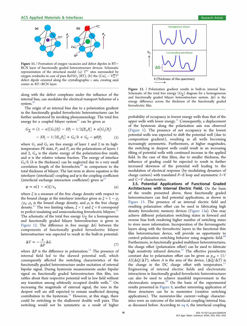
oriented along the crystallographic c axis.46 The schematicrepresentation of the formation of defect dipoles is shown inFigure 11. We believe that the dynamics of such point defects,
Figure 9. | Built-in bias assisted photovoltaic effect in functionallygraded architecture. Current density versus voltage plots under photoillumination for a bilayer 0.35(BT)−0.65(BT−BCN) thin filmarchitecture.
Figure 10. | Asymmetric capacitance−voltage plots due to built-in biasin functionally graded thin film heterostructure devices. Capacitanceversus voltage plots for (a) BT−BCN single layer, (b) 0.5(BT)−0.5(BT−BCN) bilayer with equal thickness, (c) 0.35(BT)−0.65(BT−BCN) bilayer with unequal thickness, and (d) 0.35(BT−BCN)−0.30(BT)−0.35(BT−BCN) trilayer functionally graded thin films.(Insets) Capacitance versus voltage plots measured under similarconditions but with bottom electrode as drive and top electrode asreturn.
ACS Applied Materials & Interfaces Research Article
DOI: 10.1021/acsami.5b06544ACS Appl. Mater. Interfaces XXXX, XXX, XXX−XXX
G
along with the defect complexes under the influence of theinternal bias, can modulate the electrical transport behavior of asystem.47
The origin of an internal bias due to a polarization gradientin the functionally graded ferroelectric heterostructures can befurther understood by invoking phenomenology. The total freeenergy for a coupled bilayer system11 can be given as
α ξ α
ψ
= − − − +
− − + + −
∑G G P EP E P G P
EP E P G h G PP
(1 )[ ( ) 1/2 ] [ ( )
1/2 ] /
i
i S el
1 1 1 1 1 2 2
2 2 2 1 2 (5)
where G1 and G2 are free energy of layer 1 and 2 in its high-temperature PE state, P1 and P2 are the polarizations of layers 1and 2, Gel is the elastic energy of the polarization-free misfit,and α is the relative volume fraction. The energy of interfaceGS/h (h is the thickness) can be neglected due to a very smallcorrelation length of the ferroelectric48 in comparison to thetotal thickness of bilayer. The last term in above equation is theinterlayer (interfacial) coupling and ψ is the coupling coefficient(interfacial exchange interaction coefficient) given as11
ψ α α ξ ε= −(1 ) / 0 (6)
where ξ is a measure of the free charge density with respect tothe bound charge at the interlayer interface given as ξ = 1 − ρf/ρb; ρb is the bound charge density; and ρf is the free chargedensity.11 The two limiting values, ξ = 1 and ξ = 0 correspondto perfect insulating and semiconducting ferroelectric bilayers.11
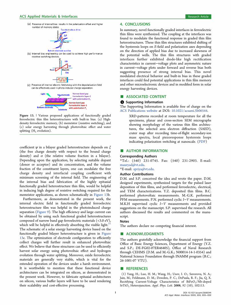
The schematic of the total free energy G∑ for a homogeneousand functionally graded bilayer heterostructure is given inFigure 12. The difference in free energy ΔG between thecomponents of functionally graded ferroelectric bilayerheterostructure was expected to result in the built-in potential:
Δ = −Δ
ΔVxP
G(7)
where ΔP is the difference in polarization.11 The presence ofinternal field led to the skewed potential well, whichconsequently affected the switching characteristics of thefunctionally graded heterostructure under excitation of externalbipolar signal. During hysteresis measurements under bipolarsignal on functionally graded heterostructure thin film, ionrattles about their respective potential well in low field withoutany transition among arbitrarily occupied double wells.11 Onincreasing the magnitude of external signal, the ions in thedeepest well are still expected to remain unaffected denyingcontribution to the hysteresis.11 However, at this stage, therecould be switching in the shallowest double well pairs. Thisswitching would not be symmetric as a result of higher
probability of occupancy in lowest energy wells than that of theupper wells with lower energy.11 Consequently, a displacementof the hysteresis along the polarization axis was observed(Figure 5). The presence of net occupancy in the lowestpotential wells was expected to shift the potential well (due tocomposition gradient), resulting in all wells becomingincreasingly asymmetric. Furthermore, at higher magnitudes,the switching in deepest wells could result in an increasingtilting of potential wells with continued increase in the appliedfield. In the case of thin films, due to smaller thickness, theinfluence of grading could be expected to result in furtherincreased skewness of the potential well leading to themodulation of electrical response (by modulating dynamics ofcharge carriers) with translated P−E loop and asymmetric I−Vand C−V characteristics.
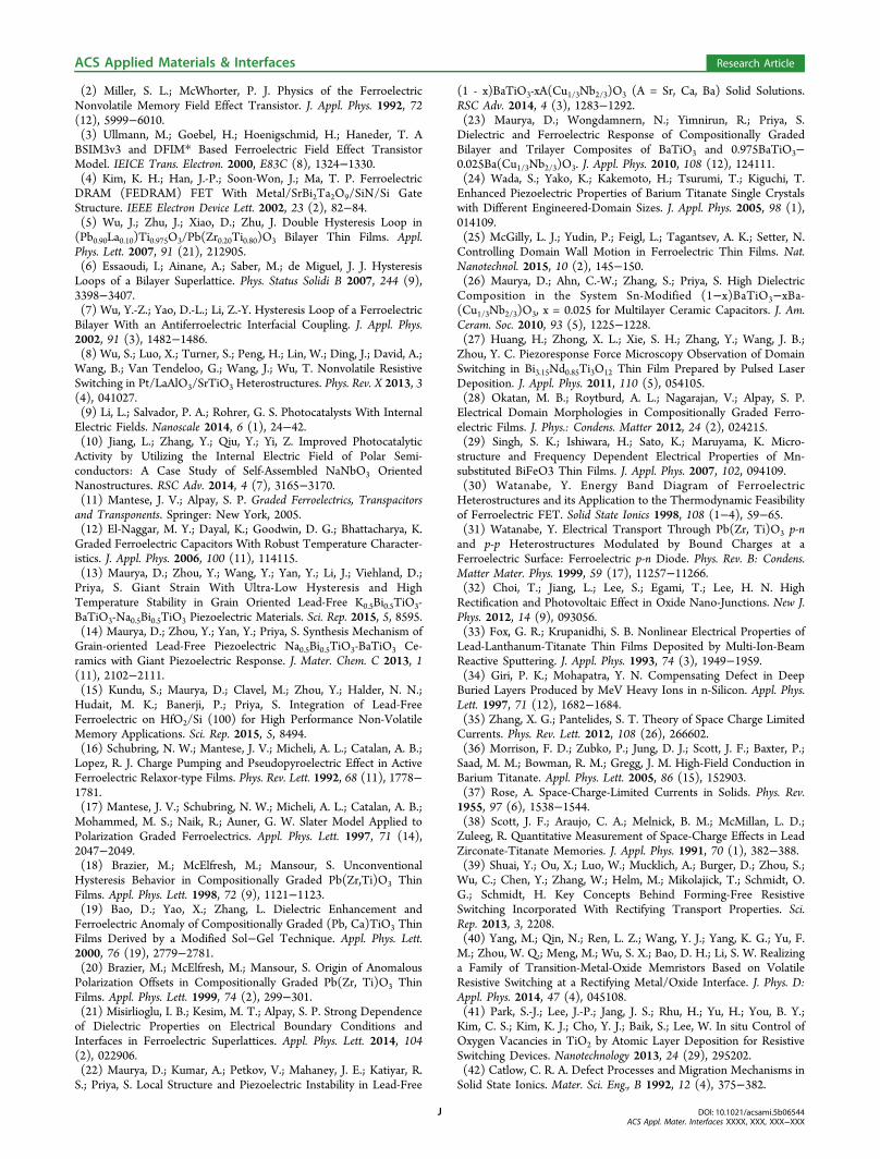
3.5. Potential Applications of Functional GradedArchitectures with Internal Electric Field. On the basisof the results presented above, these functionally gradedheterostructures can find potential applications, as shown inFigure 13. The presence of an internal electric field andresulting polarization offset can be used in fabricating highdensity ferroelectric memory devices (Figure 13a). One mayachieve different polarization switching states in forward andreverse bias both rendering higher number of switching statesto store more information. Incorporation of the ferromagneticlayers along with the ferroelectric layers in the functional thinfilm heterostructure device, will provide an opportunity tocontrol polarization switching behavior using magnetic field.49
Furthermore, in functionally graded multilayer heterostructures,the charge offset (polarization offset) can be used to fabricatehigh sensitivity infrared detector.11 The effective pyroelectricconstant due to polarization offset can be given as peff = (1/A)(ΔQ/ΔT), where A is the area of the device, (ΔQ/ΔT) isthe change in the DC charge offset with temperature.11
Engineering of internal electric fields and electrostaticinteractions in functionally graded ferroelectric heterostructurescan also be used to achieve manifold improvement in theelectrocaloric response.50 On the basis of the experimentalresults presented in Figure 8, another interesting application ofthese structures can be in memristor (resistive switchingapplications). The memristor-like current−voltage character-istics were an outcome of the interfacial coupling/internal bias,as discussed before. According to eq 6, the interfacial coupling
Figure 11. | Formation of oxygen vacancies and defect dipoles in BT−BCN layer of functionally graded heterostructure devices. Schematicrepresentation of the structural model (a) T4+ sites surrounded byoxygen octahedra in case of pure BaTiO3 (BT), (b) the (CuTi″ − VO
••)×
defect dipole oriented along the crystallographic c axis, creating axialcenter in BT−BCN layer.
Figure 12. | Polarization gradient results in built-in internal bias.Schematic of the total free energy (G∑) diagram for a homogeneousand functionally graded bilayer heterostructure system. ΔG is theenergy difference across the thickness of the functionally gradedferroelectric film.
ACS Applied Materials & Interfaces Research Article
DOI: 10.1021/acsami.5b06544ACS Appl. Mater. Interfaces XXXX, XXX, XXX−XXX
H
coefficient ψ in a bilayer graded heterostructure depends on ξ(the free charge density with respect to the bound chargedensity) and α (the relative volume fraction in a bilayer).Depending upon the application, by selecting suitable dopant(donor or acceptor) and its concentration, and the volumefraction of the constituent layers, one can modulate the freecharge density and interfacial coupling coefficient withminimum screening of the internal field. The engineering ofthe internal bias and fabrication of the highly epitaxialfunctionally graded heterostructure thin film, would be helpfulin inducing high degree of resistive switching required for thememristor applications, as shown schematically in Figure 13b.Furthermore, as demonstrated in the present work, the
internal electric field in functionally graded ferroelectricheterostructure film was helpful in the photoinduced chargeseparation (Figure 9). The high efficiency and large current canbe obtained by using such functional graded heterostructurescomposed of narrow band gap ferroelectric materials (<3.0 eV),which will be helpful in effectively absorbing the visible light.51
The schematic of a solar energy harvesting device based on thefunctionally graded bilayer heterostructure is given in Figure13c. The optimization of electrode configuration to efficientlycollect charges will further result in enhanced photovoltaiceffect. We believe that these structures can be used to efficientlyharvest solar energy using photovoltaic effect and hydrogenevolution through water splitting. Moreover, oxide ferroelectricmaterials are generally very stable, which is vital for theextended operation of the devices under a harsh environment.It is worthwhile to mention that these functional devicearchitectures can be integrated on silicon, as demonstrated inthe present work. However, to fabricate epitaxial architectureson silicon, various buffer layers will have to be used renderingtheir scalability and cost-effective processing.
4. CONCLUSIONSIn summary, novel functionally graded interfaces in ferroelectricthin films were synthesized. The coupling at the interfaces wasfound to modulate the functional response in graded thin filmheterostructures. These thin film structures exhibited shifting ofthe hysteresis loops on E-field and polarization axes dependingon the direction of applied bias due to increased skewness ofthe potential wells. The thin film structures with gradedinterfaces further exhibited diode-like high rectificationcharacteristics in current−voltage plots and asymmetric naturein current−voltage plots under forward and reverse bias bothsuggesting presence of strong internal bias. This novelmodulated electrical behavior and built-in bias in these gradedinterfaces could find potential applications in thin film memoryand other microelectronic devices and in modified form in solarenergy harvesting devices.
■ ASSOCIATED CONTENT*S Supporting InformationThe Supporting Information is available free of charge on theACS Publications website at DOI: 10.1021/acsami.5b06544.
XRD-patterns recorded at room temperature for all thespecimens, planar and cross-section SEM micrographsshowing morphology of the various thin film architec-tures, the selected area electron diffraction (SAED),crater map after recording time-of-flight secondary-ionmass spectra, local piezoresponse hysteresis loopsindicating polarization switching at nanoscale. (PDF)
■ AUTHOR INFORMATIONCorresponding Authors*Tel.: (540) 231-0745. Fax: (540) 231-2903. E-mail:[email protected].*E-mail: [email protected] ContributionsD.M. and S.P. conceived the idea and wrote the paper. D.M.designed experiments, synthesized targets for the pulsed laserdeposition of thin films, and performed ferroelectric, electrical,and TEM characterizations. Y.Z. deposited thin films. B.C.performed photovoltaic measurements. M.-G.K. performedPFM measurements. P.N. performed cyclic I−V measurements.M.K.H supervised cyclic I−V measurements and providedsuggestions on the manuscript. S.P. supervised the research. Allauthors discussed the results and commented on the manu-script.NotesThe authors declare no competing financial interest.
■ ACKNOWLEDGMENTSThe authors gratefully acknowledge the financial support fromOffice of Basic Energy Sciences, Department of Energy (Y.Z.and S.P.; DE-FG02-07ER46405), Office of Naval Researchthrough CEHMS (D.M. and M.-G.K.; N00014-14-1-0354) andNational Science Foundation through INAMM program (B.C.;26-1001-07 VTU).
■ REFERENCES(1) Yang, H.; Luo, H. M.; Wang, H.; Usov, I. O.; Suvorova, N. A.;Jain, M.; Feldmann, D. M.; Dowden, P. C.; DePaula, R. F.; Jia, Q. X.Rectifying Current-Voltage Characteristics of BiFeO3/Nb-dopedSrTiO3 Heterojunction. Appl. Phys. Lett. 2008, 92 (10), 102113.
Figure 13. | Various proposed applications of functionally gradedferroelectric thin film heterostructures with built-in bias. (a) High-density ferroelectric memory, (b) memristor (resistive switching), and(c) solar energy harvesting through photovoltaic effect and watersplitting (H2 evolution).
ACS Applied Materials & Interfaces Research Article
DOI: 10.1021/acsami.5b06544ACS Appl. Mater. Interfaces XXXX, XXX, XXX−XXX
I
(2) Miller, S. L.; McWhorter, P. J. Physics of the FerroelectricNonvolatile Memory Field Effect Transistor. J. Appl. Phys. 1992, 72(12), 5999−6010.(3) Ullmann, M.; Goebel, H.; Hoenigschmid, H.; Haneder, T. ABSIM3v3 and DFIM* Based Ferroelectric Field Effect TransistorModel. IEICE Trans. Electron. 2000, E83C (8), 1324−1330.(4) Kim, K. H.; Han, J.-P.; Soon-Won, J.; Ma, T. P. FerroelectricDRAM (FEDRAM) FET With Metal/SrBi2Ta2O9/SiN/Si GateStructure. IEEE Electron Device Lett. 2002, 23 (2), 82−84.(5) Wu, J.; Zhu, J.; Xiao, D.; Zhu, J. Double Hysteresis Loop in(Pb0.90La0.10)Ti0.975O3/Pb(Zr0.20Ti0.80)O3 Bilayer Thin Films. Appl.Phys. Lett. 2007, 91 (21), 212905.(6) Essaoudi, I.; Ainane, A.; Saber, M.; de Miguel, J. J. HysteresisLoops of a Bilayer Superlattice. Phys. Status Solidi B 2007, 244 (9),3398−3407.(7) Wu, Y.-Z.; Yao, D.-L.; Li, Z.-Y. Hysteresis Loop of a FerroelectricBilayer With an Antiferroelectric Interfacial Coupling. J. Appl. Phys.2002, 91 (3), 1482−1486.(8) Wu, S.; Luo, X.; Turner, S.; Peng, H.; Lin, W.; Ding, J.; David, A.;Wang, B.; Van Tendeloo, G.; Wang, J.; Wu, T. Nonvolatile ResistiveSwitching in Pt/LaAlO3/SrTiO3 Heterostructures. Phys. Rev. X 2013, 3(4), 041027.(9) Li, L.; Salvador, P. A.; Rohrer, G. S. Photocatalysts With InternalElectric Fields. Nanoscale 2014, 6 (1), 24−42.(10) Jiang, L.; Zhang, Y.; Qiu, Y.; Yi, Z. Improved PhotocatalyticActivity by Utilizing the Internal Electric Field of Polar Semi-conductors: A Case Study of Self-Assembled NaNbO3 OrientedNanostructures. RSC Adv. 2014, 4 (7), 3165−3170.(11) Mantese, J. V.; Alpay, S. P. Graded Ferroelectrics, Transpacitorsand Transponents. Springer: New York, 2005.(12) El-Naggar, M. Y.; Dayal, K.; Goodwin, D. G.; Bhattacharya, K.Graded Ferroelectric Capacitors With Robust Temperature Character-istics. J. Appl. Phys. 2006, 100 (11), 114115.(13) Maurya, D.; Zhou, Y.; Wang, Y.; Yan, Y.; Li, J.; Viehland, D.;Priya, S. Giant Strain With Ultra-Low Hysteresis and HighTemperature Stability in Grain Oriented Lead-Free K0.5Bi0.5TiO3-BaTiO3-Na0.5Bi0.5TiO3 Piezoelectric Materials. Sci. Rep. 2015, 5, 8595.(14) Maurya, D.; Zhou, Y.; Yan, Y.; Priya, S. Synthesis Mechanism ofGrain-oriented Lead-Free Piezoelectric Na0.5Bi0.5TiO3-BaTiO3 Ce-ramics with Giant Piezoelectric Response. J. Mater. Chem. C 2013, 1(11), 2102−2111.(15) Kundu, S.; Maurya, D.; Clavel, M.; Zhou, Y.; Halder, N. N.;Hudait, M. K.; Banerji, P.; Priya, S. Integration of Lead-FreeFerroelectric on HfO2/Si (100) for High Performance Non-VolatileMemory Applications. Sci. Rep. 2015, 5, 8494.(16) Schubring, N. W.; Mantese, J. V.; Micheli, A. L.; Catalan, A. B.;Lopez, R. J. Charge Pumping and Pseudopyroelectric Effect in ActiveFerroelectric Relaxor-type Films. Phys. Rev. Lett. 1992, 68 (11), 1778−1781.(17) Mantese, J. V.; Schubring, N. W.; Micheli, A. L.; Catalan, A. B.;Mohammed, M. S.; Naik, R.; Auner, G. W. Slater Model Applied toPolarization Graded Ferroelectrics. Appl. Phys. Lett. 1997, 71 (14),2047−2049.(18) Brazier, M.; McElfresh, M.; Mansour, S. UnconventionalHysteresis Behavior in Compositionally Graded Pb(Zr,Ti)O3 ThinFilms. Appl. Phys. Lett. 1998, 72 (9), 1121−1123.(19) Bao, D.; Yao, X.; Zhang, L. Dielectric Enhancement andFerroelectric Anomaly of Compositionally Graded (Pb, Ca)TiO3 ThinFilms Derived by a Modified Sol−Gel Technique. Appl. Phys. Lett.2000, 76 (19), 2779−2781.(20) Brazier, M.; McElfresh, M.; Mansour, S. Origin of AnomalousPolarization Offsets in Compositionally Graded Pb(Zr, Ti)O3 ThinFilms. Appl. Phys. Lett. 1999, 74 (2), 299−301.(21) Misirlioglu, I. B.; Kesim, M. T.; Alpay, S. P. Strong Dependenceof Dielectric Properties on Electrical Boundary Conditions andInterfaces in Ferroelectric Superlattices. Appl. Phys. Lett. 2014, 104(2), 022906.(22) Maurya, D.; Kumar, A.; Petkov, V.; Mahaney, J. E.; Katiyar, R.S.; Priya, S. Local Structure and Piezoelectric Instability in Lead-Free
(1 - x)BaTiO3-xA(Cu1/3Nb2/3)O3 (A = Sr, Ca, Ba) Solid Solutions.RSC Adv. 2014, 4 (3), 1283−1292.(23) Maurya, D.; Wongdamnern, N.; Yimnirun, R.; Priya, S.Dielectric and Ferroelectric Response of Compositionally GradedBilayer and Trilayer Composites of BaTiO3 and 0.975BaTiO3−0.025Ba(Cu1/3Nb2/3)O3. J. Appl. Phys. 2010, 108 (12), 124111.(24) Wada, S.; Yako, K.; Kakemoto, H.; Tsurumi, T.; Kiguchi, T.Enhanced Piezoelectric Properties of Barium Titanate Single Crystalswith Different Engineered-Domain Sizes. J. Appl. Phys. 2005, 98 (1),014109.(25) McGilly, L. J.; Yudin, P.; Feigl, L.; Tagantsev, A. K.; Setter, N.Controlling Domain Wall Motion in Ferroelectric Thin Films. Nat.Nanotechnol. 2015, 10 (2), 145−150.(26) Maurya, D.; Ahn, C.-W.; Zhang, S.; Priya, S. High DielectricComposition in the System Sn-Modified (1−x)BaTiO3−xBa-(Cu1/3Nb2/3)O3, x = 0.025 for Multilayer Ceramic Capacitors. J. Am.Ceram. Soc. 2010, 93 (5), 1225−1228.(27) Huang, H.; Zhong, X. L.; Xie, S. H.; Zhang, Y.; Wang, J. B.;Zhou, Y. C. Piezoresponse Force Microscopy Observation of DomainSwitching in Bi3.15Nd0.85Ti3O12 Thin Film Prepared by Pulsed LaserDeposition. J. Appl. Phys. 2011, 110 (5), 054105.(28) Okatan, M. B.; Roytburd, A. L.; Nagarajan, V.; Alpay, S. P.Electrical Domain Morphologies in Compositionally Graded Ferro-electric Films. J. Phys.: Condens. Matter 2012, 24 (2), 024215.(29) Singh, S. K.; Ishiwara, H.; Sato, K.; Maruyama, K. Micro-structure and Frequency Dependent Electrical Properties of Mn-substituted BiFeO3 Thin Films. J. Appl. Phys. 2007, 102, 094109.(30) Watanabe, Y. Energy Band Diagram of FerroelectricHeterostructures and its Application to the Thermodynamic Feasibilityof Ferroelectric FET. Solid State Ionics 1998, 108 (1−4), 59−65.(31) Watanabe, Y. Electrical Transport Through Pb(Zr, Ti)O3 p-nand p-p Heterostructures Modulated by Bound Charges at aFerroelectric Surface: Ferroelectric p-n Diode. Phys. Rev. B: Condens.Matter Mater. Phys. 1999, 59 (17), 11257−11266.(32) Choi, T.; Jiang, L.; Lee, S.; Egami, T.; Lee, H. N. HighRectification and Photovoltaic Effect in Oxide Nano-Junctions. New J.Phys. 2012, 14 (9), 093056.(33) Fox, G. R.; Krupanidhi, S. B. Nonlinear Electrical Properties ofLead-Lanthanum-Titanate Thin Films Deposited by Multi-Ion-BeamReactive Sputtering. J. Appl. Phys. 1993, 74 (3), 1949−1959.(34) Giri, P. K.; Mohapatra, Y. N. Compensating Defect in DeepBuried Layers Produced by MeV Heavy Ions in n-Silicon. Appl. Phys.Lett. 1997, 71 (12), 1682−1684.(35) Zhang, X. G.; Pantelides, S. T. Theory of Space Charge LimitedCurrents. Phys. Rev. Lett. 2012, 108 (26), 266602.(36) Morrison, F. D.; Zubko, P.; Jung, D. J.; Scott, J. F.; Baxter, P.;Saad, M. M.; Bowman, R. M.; Gregg, J. M. High-Field Conduction inBarium Titanate. Appl. Phys. Lett. 2005, 86 (15), 152903.(37) Rose, A. Space-Charge-Limited Currents in Solids. Phys. Rev.1955, 97 (6), 1538−1544.(38) Scott, J. F.; Araujo, C. A.; Melnick, B. M.; McMillan, L. D.;Zuleeg, R. Quantitative Measurement of Space-Charge Effects in LeadZirconate-Titanate Memories. J. Appl. Phys. 1991, 70 (1), 382−388.(39) Shuai, Y.; Ou, X.; Luo, W.; Mucklich, A.; Burger, D.; Zhou, S.;Wu, C.; Chen, Y.; Zhang, W.; Helm, M.; Mikolajick, T.; Schmidt, O.G.; Schmidt, H. Key Concepts Behind Forming-Free ResistiveSwitching Incorporated With Rectifying Transport Properties. Sci.Rep. 2013, 3, 2208.(40) Yang, M.; Qin, N.; Ren, L. Z.; Wang, Y. J.; Yang, K. G.; Yu, F.M.; Zhou, W. Q.; Meng, M.; Wu, S. X.; Bao, D. H.; Li, S. W. Realizinga Family of Transition-Metal-Oxide Memristors Based on VolatileResistive Switching at a Rectifying Metal/Oxide Interface. J. Phys. D:Appl. Phys. 2014, 47 (4), 045108.(41) Park, S.-J.; Lee, J.-P.; Jang, J. S.; Rhu, H.; Yu, H.; You, B. Y.;Kim, C. S.; Kim, K. J.; Cho, Y. J.; Baik, S.; Lee, W. In situ Control ofOxygen Vacancies in TiO2 by Atomic Layer Deposition for ResistiveSwitching Devices. Nanotechnology 2013, 24 (29), 295202.(42) Catlow, C. R. A. Defect Processes and Migration Mechanisms inSolid State Ionics. Mater. Sci. Eng., B 1992, 12 (4), 375−382.
ACS Applied Materials & Interfaces Research Article
DOI: 10.1021/acsami.5b06544ACS Appl. Mater. Interfaces XXXX, XXX, XXX−XXX
J
(43) Joshi, P. C.; Desu, S. B. Structural, Electrical, and OpticalStudies on Rapid Thermally Processed Ferroelectric BaTiO3 ThinFilms Prepared by Metallo-Organic Solution Deposition Technique.Thin Solid Films 1997, 300 (1−2), 289−294.(44) Eichel, R.-A. Structural and Dynamic Properties of OxygenVacancies in Perovskite Oxides-Analysis of Defect Chemistry byModern Multi-Frequency and Pulsed EPR Techniques. Phys. Chem.Chem. Phys. 2011, 13 (2), 368−384.(45) Chan, H. M.; Harmer, M. R.; Smyth, D. M. CompensatingDefects in Highly Donor-Doped BaTiO3. J. Am. Ceram. Soc. 1986, 69(6), 507−510.(46) Eichel, R.-A.; Erhart, P.; Traskelin, P.; Albe, K.; Kungl, H.;Hoffmann, M. J. Defect-Dipole Formation in Copper-Doped PbTiO3Ferroelectrics. Phys. Rev. Lett. 2008, 100 (9), 095504.(47) Ren, X. Large Electric-Field-Induced Strain in FerroelectricCrystals by Point-Defect-Mediated Reversible Domain Switching. Nat.Mater. 2004, 3 (2), 91−94.(48) Strukov, B.; Levanyuk, A. Ferroelectric Phenomena in Crystals.Springer: New York, 1998.(49) Valencia, S.; Crassous, A.; Bocher, L.; Garcia, V.; Moya, X.;Cherifi, R. O.; Deranlot, C.; Bouzehouane, K.; Fusil, S.; Zobelli, A.;Gloter, A.; Mathur, N. D.; Gaupp, A.; Abrudan, R.; Radu, F.;Barthelemy, A.; Bibes, M. Interface-Induced Room-TemperatureMultiferroicity in BaTiO3. Nat. Mater. 2011, 10, 753−758.(50) Kesim, M. T.; Zhang, J.; Alpay, S. P.; Martin, L. W. EnhancedElectrocaloric and Pyroelectric Response from Ferroelectric Multi-layers. Appl. Phys. Lett. 2014, 105 (5), 052901.(51) Nechache, R.; Harnagea, C.; Li, S.; Cardenas, L.; Huang, W.;Chakrabartty, J.; Rosei, F. Bandgap Tuning of Multiferroic Oxide SolarCells. Nat. Photonics 2015, 9, 61−67.
ACS Applied Materials & Interfaces Research Article
DOI: 10.1021/acsami.5b06544ACS Appl. Mater. Interfaces XXXX, XXX, XXX−XXX
K


![International Journal of Adhesion and Adhesiveskshanmugam.faculty.masdar.ac.ae/PDF/Tippi.pdf · 23]. Such functionally graded interfaces (gradation of elastic properties over the](https://img.pdfslide.us/doc/110x75/5e87e03132dbc349a573f4eb/international-journal-of-adhesion-and-23-such-functionally-graded-interfaces-gradation.jpg)