Embed Size (px)
Citation preview

FUNCTIONAL OVERVIEW
Design a synchronous 4-bit up and down counter
Operates at 25MHz on the positive edge of the clock
Designed to drive a 10pF capacitive load Latches a valu e at any point by toggling the
enable
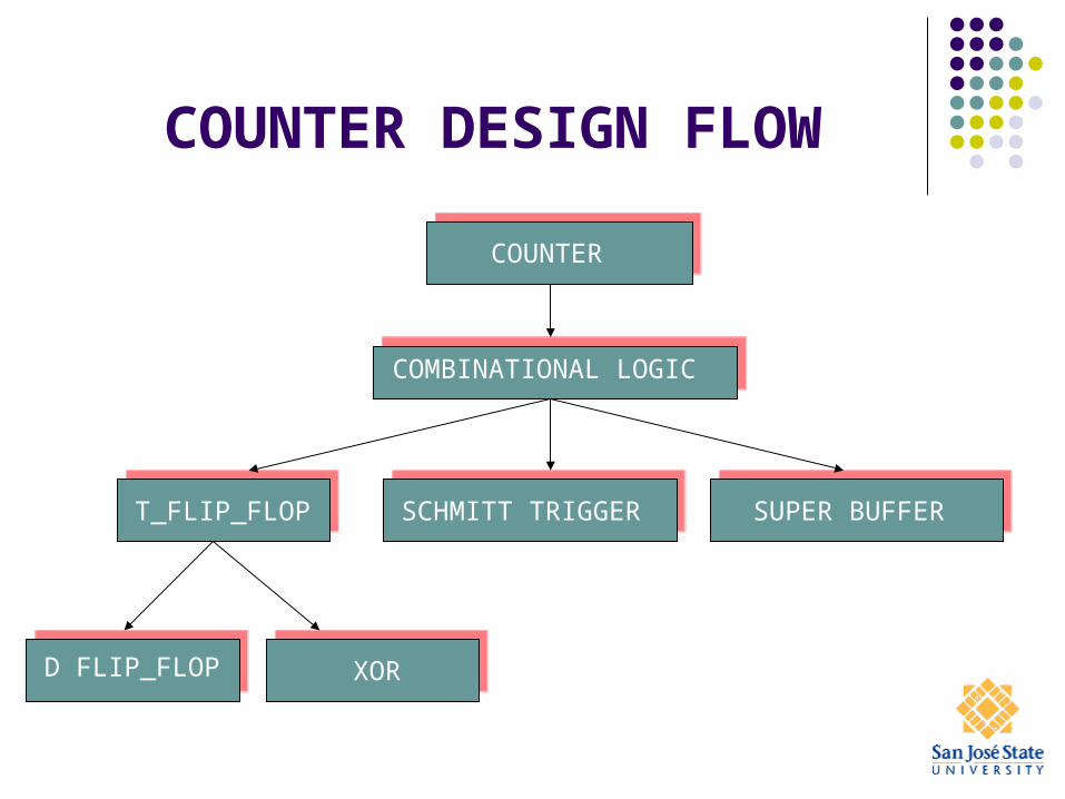
COUNTER DESIGN FLOW
COUNTER
T_FLIP_FLOP
D FLIP_FLOP XOR
SCHMITT TRIGGER SUPER BUFFER
COMBINATIONAL LOGIC

SCHEMATIC

COUNTER TESTBENCH

LAYOUT

SIGNAL FLOW
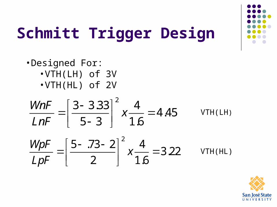
Schmitt Trigger Design
23 3.33 4
4.455 3 1.6
WnFx
LnF
•Designed For:•VTH(LH) of 3V•VTH(HL) of 2V
VTH(LH)
VTH(HL)
25 .73 2 4
3.222 1.6
WpFx
LpF

Schmitt Layout

Schmitt Trigger Validation
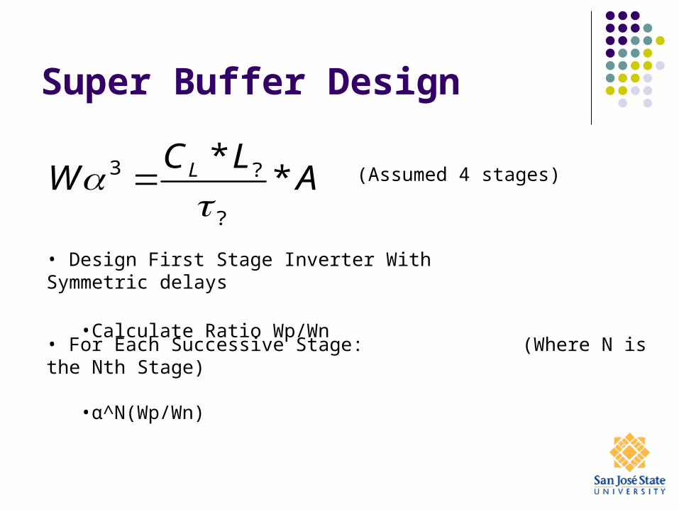
Super Buffer Design
3 ?
?
**LC L
W A
(Assumed 4 stages)
• Design First Stage Inverter With Symmetric delays
•Calculate Ratio Wp/Wn
• For Each Successive Stage: (Where N is the Nth Stage)
•α^N(Wp/Wn)

Test Bench Output

French Fried Design
2
7.612.6
.6 4 *1 5
mAWidth uM
AE cm E
cm
•I(max) for AL (Metal 1) = 1 x 10^5 A/cm^2
•Our Buffer: 5.27 x 10^5 A/cm^2

Super Buffer Layout

T-Flip Flop Schematic
Preset
Clear
Clock
Enable

T-Flip Flop Layout

T-FF Transient Response

T-FF Transient Response

H-Tree Clocking Scheme

Conclusion
4 Bit Counter with up and down count capability Preset, Clear, Enable Inputs Operates at 25Mhz Clock Frequency with a
delay of 6ns from Super Buffer. Input Noise Immunity 2.5V +/- 20% Output power of 60mW Driving 10pF Load Total Area of 406um x 925um = 3.76e-3cm^2