Embed Size (px)
Citation preview

The IR3220S is a fully protected dual high side switch I.C thatintegrates an H–bridge motor controller with two very efficienthigh side MOSFETs in a single 20-pin package. The IR3220Scombines with the two low side IRF7484Q MOSFETs as few as10 external passive components to provide a complete, fully op-erational and fully protected H-bridge control actuator with for-ward, reverse, braking and non-braking modes without the needof a micro-controller.
Functional DescriptionThe high side switches provide the direction capability and the H-bridge protection. The low side MOSFETs bring the flexibility byoffering the high frequency switching ability. Therefore, crudestart-up of the motor is avoided and replaced by a smooth andstress-less speed ramp-up.
The IR3220S features shoot-through protection for each leg, H-bridge logic control, soft-start sequence and over-current / over-temperature shutdown protections. Two input signals (IN1 & IN2)select the operating modes while the PWM soft-start sequencecycles the corresponding active low side MOSFET in order tolimit the motor in-rush current. The soft-start sequence is pro-grammed by an RC time constant and reset itself automatically.Thanks to the inner PWM oscillator, the IR3220S can also bethe final stage of an overall torque or speed loop. If needed, anexternal clock may force the H-bridge switching operation. Thiscan be combined with low frequency PWM operation throughthe IN1(2) inputs.
The IR3220S is a Co-pack IPS product offering very low Rds(on)and a high level of functionality and protection. Its open architec-ture and programmability helps the designer to optimize eachmotor drive upon the application requirements at a very low cost.For automotive actuators, the motor is kept shorted even duringthe low consumption sleep mode. Shoot-through protection, over-temperature & over-current shutdowns, self-adaptive dead-timeand PWM circuitries are described in details in the AN 1032Application Note. A general purpose method to help rating thesoft-start sequence as well as layout and thermal considerationsare also covered. Finally, a 6A DC motor actuator with a PCBsize down to 1 Inch² is suggested in the document.
IR3220S
Data Sheet No.PD60180-C
FULLY PROTECTED H-BRIDGE FOR D.C. MOTORFeatures
8-Lead SOICIRF7484Q
Packages
20-Lead SOIC(wide body)
www.irf.com 1
Programmable PWM In-rushCurrent Limitation (e.g 18A)
6 A Continuous Current Capability
without Heat Sink (2 x 13 mΩΩΩΩΩ)
Over-Temperature (165 °C) andOver-Current (30A) Protections
20 kHz PWM Oscillator Embedded
Low & High Frequency SwitchingOperation (self adaptive dead-time)
Easy Speed / Torque Control(analog duty cycle input)
Braking / Non-Braking Modes
Sleep Mode (braking) forAutomotive Actuator
IR3220S
2 WWW.IRF.COM
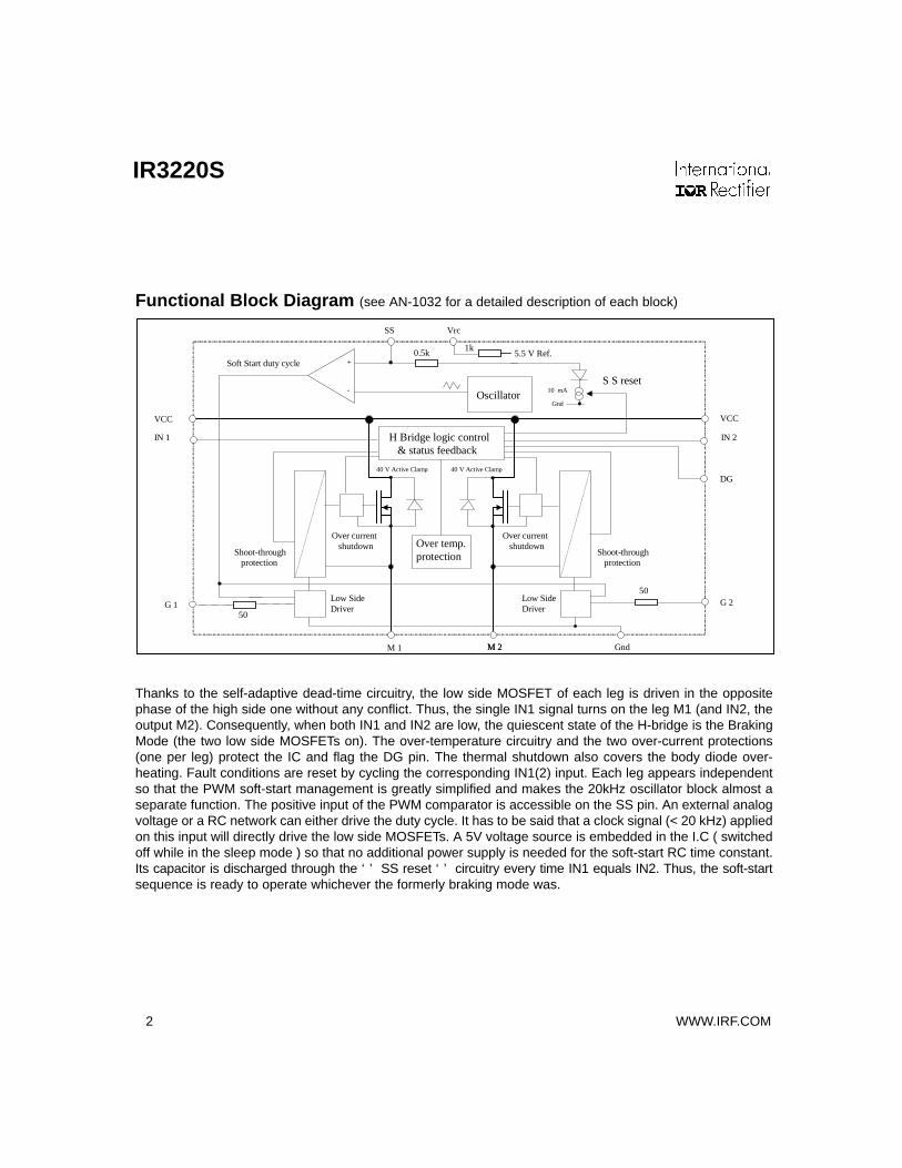
Functional Block Diagram (see AN-1032 for a detailed description of each block)
H Bridge logic control & status feedback
VCC VCC
SS
DG
IN 1 IN 2
Shoot-through protection
M 2
G 1
M 1 M 2
G 2
Oscillator
Gnd
Gnd
+ -
Soft Start duty cycle S S reset
Over current shutdown Over temp.
protection
Vrc
5.5 V Ref.
10 mA
Over current shutdown
Shoot-through protection
Low Side Driver
Low Side Driver
40 V Active Clamp 40 V Active Clamp
1k
50
50
0.5k
Thanks to the self-adaptive dead-time circuitry, the low side MOSFET of each leg is driven in the oppositephase of the high side one without any conflict. Thus, the single IN1 signal turns on the leg M1 (and IN2, theoutput M2). Consequently, when both IN1 and IN2 are low, the quiescent state of the H-bridge is the BrakingMode (the two low side MOSFETs on). The over-temperature circuitry and the two over-current protections(one per leg) protect the IC and flag the DG pin. The thermal shutdown also covers the body diode over-heating. Fault conditions are reset by cycling the corresponding IN1(2) input. Each leg appears independentso that the PWM soft-start management is greatly simplified and makes the 20kHz oscillator block almost aseparate function. The positive input of the PWM comparator is accessible on the SS pin. An external analogvoltage or a RC network can either drive the duty cycle. It has to be said that a clock signal (< 20 kHz) appliedon this input will directly drive the low side MOSFETs. A 5V voltage source is embedded in the I.C ( switchedoff while in the sleep mode ) so that no additional power supply is needed for the soft-start RC time constant.Its capacitor is discharged through the ‘’ SS reset ‘’ circuitry every time IN1 equals IN2. Thus, the soft-startsequence is ready to operate whichever the formerly braking mode was.

IR3220S
WWW.IRF.COM 3
Soft-Start Sequence
t t t
IN1 (IN2) SS M1-M2 (M2-M1) Duty cycle modulation follows SS voltage
Tss ( approximately 1.4 x RC time constant ) Trd
Vss+ Vss-
Truth Table IN1 IN2 MODES DG HS1 LSS1 HS2 LSS2 SS reset
L L Stand-by with braking - sleep mode** H OFF ON OFF ON ONL H Forward rotation (normal operation) H OFF ON* ON OFF OFFL H Forward rotation (protection triggered) L OFF ON* OFF OFF OFFH L Reverse rotation (normal operation) H ON OFF OFF ON* OFFH L Reverse rotation (protection triggered) L OFF OFF OFF ON* OFFH H Stand-by without braking H OFF OFF OFF OFF ON
* During Soft-start sequence, the low side part is switching. ** Protections are reset in this mode
The IR 3220S over-current is set at 30A which is low enough to protect the whole application. The soft-start RCtime constant has to be designed in order to keep the maximum in-rush current below the I shutdown (applicationworst case - see AN 1032 ). The total switching sequence is about 1.4 times the RC time constant. A smootherstart-up is even achievable by slightly increasing the RC values. However, the soft-start sequence shouldremain short enough not to trip the over-temperature protection (Tj while free-wheeling). The truth table showsthat the soft-start sequence can be interrupted at any time. But a minimum time is needed prior to any changein the direction or re-start of a new SS sequence. Actually, the capacitor of the RC network has to be dischargedand the motor fully stopped first otherwise the over-current protection might trip during the next turn-on.
The protections turn off the high side MOSFETs so that no braking sequence follows the fault detection. BothIN1 and IN2 have to go low for a minimum time in order to reset the fault circuitry. When both inputs are backto the low level, the H-bridge is in the braking mode and the motor shorted. In this mode, no protection isactivated and the peak current due to the braking is not monitored. After 300 ms, the I.C sleep mode isactivated and the consumption is reduced down to few micro-amps. The low side gate drivers keep the gateshigh so the motor remains shorted. When using end switches, the I.C goes into the low consumption mode assoon as the mechanical stop are reached. When interfacing such switches directly to the IR 3220S, de-bounc-ing RC networks have to be implemented on the input pins in order to prevent false over-current detection.

IR3220S
4 WWW.IRF.COM
Typical Connection
t t t t t t
IN1 IN2 SS M1 M2 Motor Current
Braking Mode (M1 & M2 grounded)
Stand-by Mode (M1 & M2 opened)
Soft-Start sequence
IN1(2) & M1(2) Timing Diagrams
LS gate 1 LS gate 2
VCC
SS DG
IN 1 IN 2 M 1 M 2
D
S
Micro Controller
Clockwise motion
Diagnostic Feedback
Counter clockwise motion
Electrical stop
Vrc
+ 5 V Gnd
Electrical stop
D
S G SO 8 Mosfet
IR 3220
G SO 8 Mosfet
0 V
+ Bat. 10 k
10 k
10 k
R
C Deboucing RC networks ( e.g 10 nF )
1 k 1 k
S
IR3220S
WWW.IRF.COM 5
The PWM generator is based on a 3V saw-tooth oscillator. The soft-start sequence takes advantage of the RCcharge profile in order to perform a smooth duty cycle variation. When the SS pin is below 1.2V, no PWM signalis sent to the low side MOSFETs. When it exceeds 4.2V, they are permanently ON. By designing the proper RCnetwork, the start-up can either be very slow without any in-rush current or, fast and efficient by shortening thePWM sequence. In addition to the quiescent braking mode, the IR 3220S is able to open the four MOSFETssimultaneously if the mechanical load requires its natural slow-down (stand-by mode without braking). Thefour modes and their corresponding DC motor current profiles are summarized in the Timing Diagram.
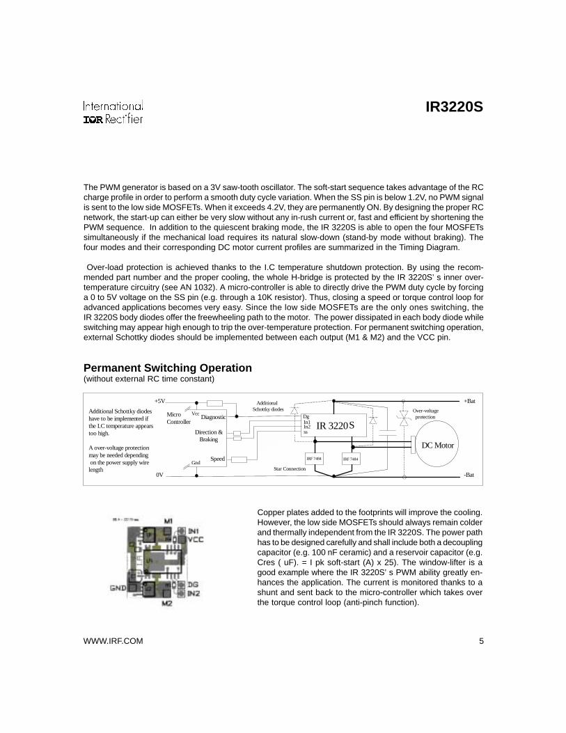
Over-load protection is achieved thanks to the I.C temperature shutdown protection. By using the recom-mended part number and the proper cooling, the whole H-bridge is protected by the IR 3220S’s inner over-temperature circuitry (see AN 1032). A micro-controller is able to directly drive the PWM duty cycle by forcinga 0 to 5V voltage on the SS pin (e.g. through a 10K resistor). Thus, closing a speed or torque control loop foradvanced applications becomes very easy. Since the low side MOSFETs are the only ones switching, theIR 3220S body diodes offer the freewheeling path to the motor. The power dissipated in each body diode whileswitching may appear high enough to trip the over-temperature protection. For permanent switching operation,external Schottky diodes should be implemented between each output (M1 & M2) and the VCC pin.
Permanent Switching Operation(without external RC time constant)
Copper plates added to the footprints will improve the cooling.However, the low side MOSFETs should always remain colderand thermally independent from the IR 3220S. The power pathhas to be designed carefully and shall include both a decouplingcapacitor (e.g. 100 nF ceramic) and a reservoir capacitor (e.g.Cres ( uF). = I pk soft-start (A) x 25). The window-lifter is agood example where the IR 3220S’s PWM ability greatly en-hances the application. The current is monitored thanks to ashunt and sent back to the micro-controller which takes overthe torque control loop (anti-pinch function).
Micro Controller
Speed
Direction & Braking
Diagnostic
+5V
0V
+Bat
-Bat
IR 3220 Dg In1 In2 ss
DC Motor
Over-voltage protection
Additional Schottky diodes Additional Schottky diodes
have to be implemented if the I.C temperature appears too high. A over-voltage protection may be needed depending on the power supply wire length Star Connection Gnd
Vcc
IRF 7484 IRF 7484
S

IR3220S
6 WWW.IRF.COM
In addition, the soft-start sequence pro-vides a smooth motion of the window.Torque or speed controls are alsoachievable without any micro-control-ler. With a few additional components,the IR 3220S can be the ‘’power stage‘’of an overall analog control loop. TheSS pin is then used as the PWM dutycycle input (continuous switching op-eration requires high cooling capabil-ity)
For actuators, the PWM Soft Start sequence helps reduce the speed before reaching the end switches. There-fore, the braking time is very short and the actuator final position is then accurate and repeatable as shownhereunder. Mechanical stops under torque control are also possible by controlling the motor current throughthe PWM duty cycle.
+Bat
-Bat
IR 3220 Dg In1 In2 ss
IRF 7484 IRF 7484
µP
Shunt
When an obstacle is encountered, the uP controls the torque thanks to the SS pin.
+ Vcc
DG
D D D D D D D D
S S S S S S G
IN 1 IN 2
DG
G1 G2 M2 M2 M2 M1 M1 M1
Vcc Vcc Vcc Vcc
GND
IR 3220
Rev
Fwd
100 nF
1000 uF
IRF7484
SS
Vrc
Gnd
C
R1
IRF7484
R2
Fwd Rev
G
speed
motion
braking braking Rev
Fwd
Soft-Start ( PWM ) Low Speed
( PWM )

IR3220S
WWW.IRF.COM 7
Thermal CharacteristicsSymbol Parameter Typ. Max. UnitsRth 1 Junction to ambient thermal resistance (std footprint) 80 —
Rth 2 Junction to ambient thermal resistance (1" sq. footprint) 60 —°C/W
Absolute maximum ratings indicate sustained limits beyond which damage to the device may occur. All voltage param-eters are referenced to Gnd lead. (TAmbient = 25oC unless otherwise specified). Symbols with (2) refer to M2 output.
Symbol Parameter Min. Max. UnitsVm1 (2) Maximum M1 (M2) voltage (active clamp) Vcc-37 Vcc+0.3Vin1 (2) Maximum IN 1 (IN 2) voltage -0.3 5.5
Vcc/gnd Maximum Vcc pin to GND pin voltage -0.3 45
I in1 (2) Maximum IN1 (IN 2) current -1 10 mA
Vg1 (2) Maximum Gate 1 ( Gate 2 ) voltage -0.3 7.5
Vss Maximum SS voltage -0.3 5.5
Vrc Maximum Vrc voltage -0.3 5.5
Irc Maximum output current of the Vrc pin — 1 mA
Vdg Maximum diagnostic output voltage -0.3 5.5 V
Idg Maximum diagnostic output current -1 10 mA
Isd cont. Diode max. permanent current (Rth=80°C/W) (1) — 2.0
(Rth=60°C/W) (1) — 3.0Isd pulsed Diode max. pulsed current (1) — 15
ESD 1 Electrostatic discharge ( human body model C=100pF, R=1500Ω) — 4
ESD 2 Electrostatic discharge ( machine model C=200pF, R=0Ω, L=10µH) — 0.5
PD Maximum power dissipation ( Rth = 80°C/W ) — 1.5 W
TJ max. Max. storage & operating junction temperature -40 +150
TL Lead temperature ( soldering 10 seconds ) — 300
Vcc/gnd max. Maximum Vcc to GND voltage (0.4 s - single pulse) — 60 V
Ig1 (2) max. Maximum transient gate current (Ton < 5µS) — 100
Ig1 (2) avg. Maximum average gate current — 10
V
V
A
° C
(1) Limited by junction temperature.
Absolute Maximum Ratings
kV
mA

IR3220S
8 WWW.IRF.COM
Symbol Parameter Min. Max. UnitsVcc Continuous Vcc voltage (2) 8 28
Vin1 (2) High level IN 1 (IN 2) input voltage 4 5.5
Vin1 (2) Low level IN 1 (IN 2) input voltage -0.3 0.9
Iout Ta=85°C Continuous output current (Std footprint - Tj = 150°C) — 6.0Iout Ta=105°C Continuous output current (Std footprint - Tj = 150°C) — 5.0
R in Recommended resistor in series with IN pin 0.5 5
R dg Recommended pull-up resistor on DG pin 10 20
R Soft-Start resistor 20 200
C Soft-Start capacitor 0.1 3.3 µF
R gate Recommended gate resistor for Low Side Switch 0 50 ΩLm min. Minimum motor inductance required 10 — µH
Recommended Operating ConditionsThese values are given for a quick design. For operation outside these conditions, please consult the application notes.
V
A
kΩ
Symbol Parameter Min. Typ. Max. Units Test ConditionsRds1 on ON state resistance Tj = 25oC — 11 13Rds2 on ON state resistance Tj = 150oC — 18 22Vcc oper. Functional voltage range 5.5 — 35Vclamp1 (2) Vcc to M1 (M2) clamp voltage 37 40 48 Id =10mA see Figs.1,2Vf1 (2) Body diode 1 (2) forward voltage — 0.9 — Id = 5A, Vin1,2 = 0V
IM1 (2) leakage M1 (M2) output leakage current — 10 50
Icc off Supply current when off (sleep mode) — 10 50Icc on Supply current when on — 8 12 mA Vin1 = 5VVdgl Low level diagnostic output voltage — 0.4 — V Idg = 1.0mAIdg leakage Diagnostic output leakage current — — 10 µA Vdg = 4.5VVih1 (2) th. IN1 (IN2) high threshold voltage — 2.6 3.4Vil1 (2) th. IN1 (IN2) low threshold voltage 1.0 2.0 —Iin1 (2) ON state IN1 (IN2) positive current — 30 80 µA Vin1, 2 = 5VVccuv+ Vcc UVLO positive going threshold — 5 —Vccuv- Vcc UVLO negative going threshold — 4 —Vss+ SS high level threshold — 4.2 4.8Vss- SS low level threshold 0.8 1.2 —Iss leakage SS pin leakage current — 0.1 10 µA Vss = 5VVrc Typical voltage of the Vrc pin — 5.3 — Irc = 0.25mAIN1(2) hys IN1 (2) input hysteresis 0.2 0.7 1.5 Iin = 1mA
Static Electrical Characteristics(Tj = 25oC, Vcc = 14V unless otherwise specified.)
mΩ Vin1,2 = 5V,1m1,2 = 5A
Vm1, 2 = 0V; Tj = 25°CVin1(2) = 0V, Vcc=12V
V
µA
V
V
V
IR3220S
WWW.IRF.COM 9
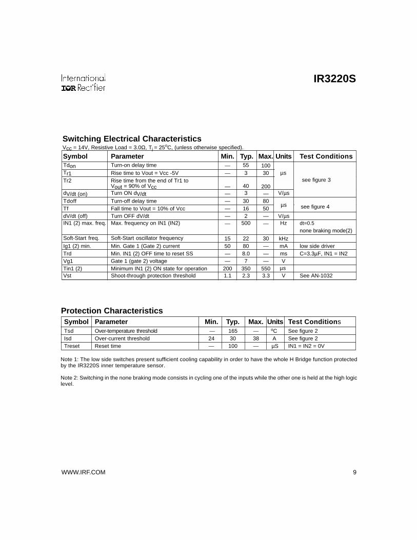
Switching Electrical CharacteristicsVcc = 14V, Resistive Load = 3.0Ω, Tj = 25oC, (unless otherwise specified).
Symbol Parameter Min. Typ. Max. Units Test ConditionsTdon Turn-on delay time — 55 100Tr1 Rise time to Vout = Vcc -5V — 3 30Tr2 Rise time from the end of Tr1 to
Vout = 90% of Vcc — 40 200dV/dt (on) Turn ON dV/dt — 3 — V/µs
Tdoff Turn-off delay time — 30 80Tf Fall time to Vout = 10% of Vcc — 16 50dV/dt (off) Turn OFF dV/dt — 2 — V/µsIN1 (2) max. freq. Max. frequency on IN1 (IN2) — 500 — Hz dt=0.5
none braking mode(2)Soft-Start freq. Soft-Start oscillator frequency 15 22 30 kHzIg1 (2) min. Min. Gate 1 (Gate 2) current 50 80 — mA low side driverTrd Min. IN1 (2) OFF time to reset SS — 8.0 — ms C=3.3µF, IN1 = IN2Vg1 Gate 1 (gate 2) voltage — 7 — VTin1 (2) Minimum IN1 (2) ON state for operation 200 350 550 µsVst Shoot-through protection threshold 1.1 2.3 3.3 V See AN-1032
see figure 3µs
µs see figure 4
Symbol Parameter Min. Typ. Max. Units Test ConditionsTsd Over-temperature threshold — 165 — oC See figure 2Isd Over-current threshold 24 30 38 A See figure 2Treset Reset time — 100 — µS IN1 = IN2 = 0V
Protection Characteristics
Note 1: The low side switches present sufficient cooling capability in order to have the whole H Bridge function protectedby the IR3220S inner temperature sensor.
Note 2: Switching in the none braking mode consists in cycling one of the inputs while the other one is held at the high logiclevel.

IR3220S
10 WWW.IRF.COM
Vcc Vcc m1 m1 m1 nc g1 G nd In1Vrc
Vcc Vcc m2 m2 m2 nc g2 In2 D g SS
Lead Assignments
20 Lead - SOIC (wide body) 8 Lead - SOIC
Part NumberIR3220S IRF7484Q
D D D D
S S S G
Vcc Positive power supply IN1 Logic input 1 ( Leg 1 Cdt. / mode )M1 Motor 1 output ( high side source - leg 1 ) IN2 Logic input 2 ( Leg 2 Cdt. / mode )M2 Motor 2 output ( high side source - leg 2 ) Dg Diagnostic output ( open drain )G1 Gate 1 drive output ( low side gate - leg 1 ) Vrc Voltage ref. output ( soft-start RC )G2 Gate 2 drive output ( low side gate - leg 2 ) SS RC soft-start input ( the voltage on this inputGnd Power supply return drives the switching duty cycle )
Lead Definitions
IR3220S
WWW.IRF.COM 11
IN1(2)
M1(2)90%
10%
Td off Tf
dV/dt off
IN 1(2)
M1 (2)
Vcc - 5 V90%Vcc
10%
Td on Tr 1 Tr 2
dV/dt on
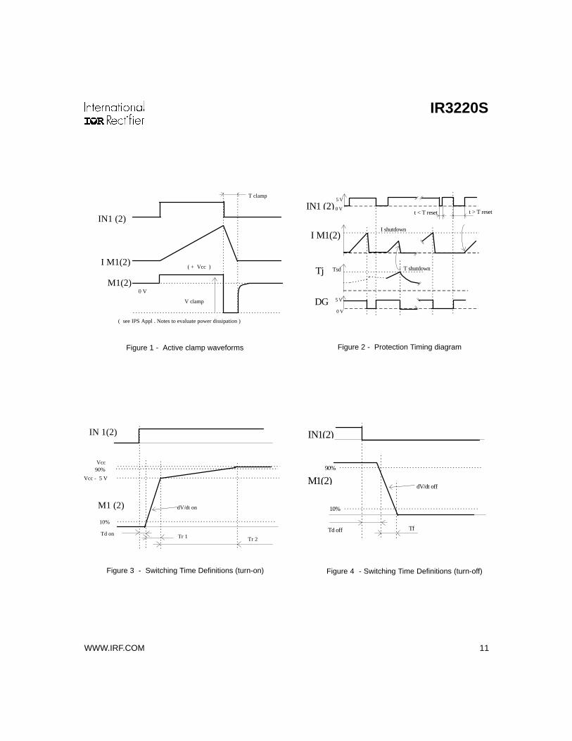
Figure 3 - Switching Time Definitions (turn-on) Figure 4 - Switching Time Definitions (turn-off)
Figure 1 - Active clamp waveforms
Tsd
IN1 (2)
I M1(2)I shutdown
Tj
t < T reset t > T reset
5 V
0 V
T shutdown
DG 5 V
0 V
I M1(2)
M1(2)
IN1 (2)
T clamp
V clamp
( + Vcc )
( see IPS Appl . Notes to evaluate power dissipation )
0 V
Figure 2 - Protection Timing diagram

IR3220S
12 WWW.IRF.COM
0
10
20
30
40
50
-50 -25 0 25 50 75 100 125 150
Figure 6 - IN1 (2) current (µA) vs Tj (oC)
0
1
2
3
4
5
-50 -25 0 25 50 75 100 125 150
----- IN1h(2) -- -- IN1l(2) - - - -IN1(2) hysteresis
Figure 5 - IN1 (2) thresholds (V) vs Tj (oC)
0
10
20
30
40
50
-50 -25 0 25 50 75 100 125 150
Figure 7 - Iccoff (µA) vs Tj (oC)
0
10
20
30
40
50
-50 -25 0 25 50 75 100 125 150
Figure 8 - Typ. I shutdown (A) vs Tj (oC)

IR3220S
WWW.IRF.COM 13
0
10
20
30
-50 -25 0 25 50 75 100 125 150
Figure 11 - Rdson (mΩ) vs Tj (oC) Figure 12 - Max. Cont. current (A) vs Amb. Temp. (oC)
0
2,5
5
7,5
10
12,5
15
-50 0 50 100 150 200
- - - 1’’ square footprint ------- standard footprint
0
5
10
15
20
0,0 0,2 0,4 0,6 0,8 1,0 1,2
V f @ 25°C
V f @ 150°C
02468
1012141618202224262830
0 2 4 6 8 10 12 14 16 18 20
Figure 9 - Body diode : Ids (A) vs Vds (V) Figure 10 - Rds(on) (mΩ) vs Vcc (V)

IR3220S
14 WWW.IRF.COM
10
100
1000
1,E-06 1,E-05 1,E-04 1,E-03 1,E-02 1,E-01 1,E+00 1,E+01 1,E+02
Figure 14 - Isd (A) vs Time (s)
0,01
0,1
1
10
100
rth std footprint
Figure 13 - Transient Rth (oC/W) vs Time (S)
Case Outline - 8 Lead SOIC
(MS-012AA) 01-0021 09

IR3220S
WWW.IRF.COM 15
IR WORLD HEADQUARTERS: 233 Kansas St., El Segundo, California 90245 Tel: (310) 252-7105 Data and specifications subject to change without notice. 9/18/2003
Case Outline
(MS-013AC) 01-3080 0020 Lead SOIC (wide body)