Embed Size (px)
Citation preview
Fully-automated optimization of gratingcouplers
LOGAN SU,1,* RAHUL TRIVEDI,1 NEIL V. SAPRA,1 ALEXANDER Y.PIGGOTT,1 DRIES VERCRUYSSE,1,2 AND JELENA VUCKOVIC1
1Ginzton Laboratory, Stanford University, Stanford, CA 94305, USA2Department of Physics, KU Leuven, Celestijnenlaan 200 D, B-3001 Leuven, Belgium*[email protected]
Abstract: We present a gradient-based algorithm to design general 1D grating couplers withoutany human input from start to finish, including a choice of initial condition. We show that we canreliably design efficient couplers to have multiple functionalities in different geometries, includingconventional couplers for single-polarization and single-wavelength operation, polarization-insensitive couplers, and wavelength-demultiplexing couplers. In particular, we design a fiber-to-chip blazed grating with under 0.2 dB insertion loss that requires a single etch to fabricate and noback-reflector.© 2018 Optical Society of America under the terms of the OSA Open Access Publishing Agreement
OCIS codes: (050.2770) Gratings; (130.0130) Integrated optics; (130.3120) Integrated optics devices.
References and links1. L. Chrostowski and M. Hochberg, Silicon Photonics design: from Devices to Systems (Cambridge University Press,
2015).2. R. Orobtchouk, A. Layadi, H. Gualous, D. Pascal, A. Koster, and S. Laval, “High-efficiency light coupling in a
submicrometric silicon-on-insulator waveguide,” Appl. Opt. 39, 5773–5777 (2000).3. A. Bozzola, L. Carroll, D. Gerace, I. Cristiani, and L. C. Andreani, “Optimising apodized grating couplers in a pure
SOI platform to -0.5 db coupling efficiency,” Opt. Express 23, 16289–16304 (2015).4. D. Taillaert, P. Bienstman, and R. Baets, “Compact efficient broadband grating coupler for silicon-on-insulator
waveguides,” Opt. Lett. 29, 2749–2751 (2004).5. X. Chen, C. Li, C. K. Fung, S. M. Lo, and H. K. Tsang, “Apodized waveguide grating couplers for efficient coupling
to optical fibers,” IEEE Photon. Technol. Lett. 22, 1156–1158 (2010).6. F. Van Laere, G. Roelkens, M. Ayre, J. Schrauwen, D. Taillaert, D. Van Thourhout, T. F. Krauss, and R. Baets,
“Compact and highly efficient grating couplers between optical fiber and nanophotonic waveguides,” J. Lightw.Technol. 25, 151–156 (2007).
7. W. S. Zaoui, M. F. Rosa, W. Vogel, M. Berroth, J. Butschke, and F. Letzkus, “Cost-effective cmos-compatible gratingcouplers with backside metal mirror and 69% coupling efficiency,” Opt. Express 20, B238–B243 (2012).
8. B. Wang, J. Jiang, and G. P. Nordin, “Compact slanted grating couplers,” Opt. Express 12, 3313–3326 (2004).9. W. D. Sacher, Y. Huang, L. Ding, B. J. Taylor, H. Jayatilleka, G.-Q. Lo, and J. K. Poon, “Wide bandwidth and high
coupling efficiency si3n4-on-SOI dual-level grating coupler,” Opt. Express 22, 10938–10947 (2014).10. A. Michaels and E. Yablonovtich, “Inverse design of near unity efficiency perfectly vertical grating couplers,” arXiv
preprint arXiv:1705.07186 (2017).11. C. Li, H. Zhang, M. Yu, and G. Lo, “Cmos-compatible high efficiency double-etched apodized waveguide grating
coupler,” Opt. Express 21, 7868–7874 (2013).12. X. Chen, D. J. Thomson, L. Crudginton, A. Z. Khokhar, and G. T. Reed, “Dual-etch apodised grating couplers for
efficient fibre-chip coupling near 1310 nm wavelength,” Opt. Express 25, 17864–17871 (2017).13. G. Roelkens, D. Van Thourhout, and R. Baets, “High efficiency silicon-on-insulator grating coupler based on a
poly-silicon overlay,” Opt. Express 14, 11622–11630 (2006).14. D. Vermeulen, S. Selvaraja, P. Verheyen, G. Lepage, W. Bogaerts, P. Absil, D. Van Thourhout, and G. Roelkens,
“High-efficiency fiber-to-chip grating couplers realized using an advanced cmos-compatible silicon-on-insulatorplatform,” Opt. Express 18, 18278–18283 (2010).
15. M. Matsumoto, “Analysis of the blazing effect in second-order gratings,” IEEE J. of Quantum Electron. 28, 2016–2023(1992).
16. B. Wang, J. Jiang, and G. P. Nordin, “Embedded slanted grating for vertical coupling between fibers and silicon-on-insulator planar waveguides,” IEEE Photon. Technol. Lett. 17, 1884–1886 (2005).
17. J. Yang, Z. Zhou, H. Jia, X. Zhang, and S. Qin, “High-performance and compact binary blazed grating coupler basedon an asymmetric subgrating structure and vertical coupling,” Opt. Lett. 36, 2614–2617 (2011).
Vol. 26, No. 4 | 19 Feb 2018 | OPTICS EXPRESS 4023
#312953 https://doi.org/10.1364/OE.26.004023 Journal © 2018 Received 10 Nov 2017; accepted 23 Jan 2018; published 7 Feb 2018

18. N. Na, H. Frish, I.-W. Hsieh, O. Harel, R. George, A. Barkai, and H. Rong, “Efficient broadband silicon-on-insulatorgrating coupler with low backreflection,” Opt. Lett. 36, 2101–2103 (2011).
19. A. Sánchez-Postigo, J. G. Wangüemert-Pérez, J. M. Luque-González, Í. Molina-Fernández, P. Cheben, C. A.Alonso-Ramos, R. Halir, J. H. Schmid, and A. Ortega-Moñux, “Broadband fiber-chip zero-order surface gratingcoupler with 0.4 db efficiency,” Opt. Lett. 41, 3013–3016 (2016).
20. J. Andkjær, S. Nishiwaki, T. Nomura, and O. Sigmund, “Topology optimization of grating couplers for the efficientexcitation of surface plasmons,” JOSA B 27, 1828–1832 (2010).
21. J. Covey and R. T. Chen, “Efficient surface normal multi-stage grating couplers in silicon based waveguides,” in“Optical Interconnects Conference, 2013 IEEE,” (IEEE, 2013), pp. 130–131.
22. W. S. Zaoui, A. Kunze, W. Vogel, M. Berroth, J. Butschke, F. Letzkus, and J. Burghartz, “Bridging the gap betweenoptical fibers and silicon photonic integrated circuits,” Opt. Express 22, 1277–1286 (2014).
23. Q. Zhong, V. Veerasubramanian, Y. Wang, W. Shi, D. Patel, S. Ghosh, A. Samani, L. Chrostowski, R. Bojko, and D. V.Plant, “Focusing-curved subwavelength grating couplers for ultra-broadband silicon photonics optical interfaces,”Opt. Express 22, 18224–18231 (2014).
24. B. Wohlfeil, L. Zimmermann, and K. Petermann, “Optimization of fiber grating couplers on SOI using advancedsearch algorithms,” Opt. Lett. 39, 3201–3203 (2014).
25. R. Shi, H. Guan, A. Novack, M. Streshinsky, A. E.-J. Lim, G.-Q. Lo, T. Baehr-Jones, and M. Hochberg, “High-efficiency grating couplers near 1310 nm fabricated by 248 nm duv lithography,” IEEE Photon. Technol. Lett. 26,1569–1572 (2014).
26. C. M. Lalau-Keraly, S. Bhargava, O. D. Miller, and E. Yablonovitch, “Adjoint shape optimization applied toelectromagnetic design,” Opt. Express 21, 21693–21701 (2013).
27. Z. Lin, A. Pick, M. Lončar, and A. W. Rodriguez, “Enhanced spontaneous emission at third-order dirac exceptionalpoints in inverse-designed photonic crystals,” Phys. Rev. Lett. 117, 107402 (2016).
28. L. F. Frellsen, Y. Ding, O. Sigmund, and L. H. Frandsen, “Topology optimized mode multiplexing in silicon-on-insulator photonic wire waveguides,” Opt. Express 24, 16866–16873 (2016).
29. D. Sell, J. Yang, S. Doshay, R. Yang, and J. A. Fan, “Large-angle, multifunctional metagratings based on freeformmultimode geometries,” Nano Lett. 17, 3752–3757 (2017).
30. L. Su, A. Y. Piggott, N. V. Sapra, J. Petykiewicz, and J. Vučković, “Inverse design and demonstration of a compacton-chip narrowband three-channel wavelength demultiplexer,” ACS Photonics, posted ahead of press (2017).
31. A. Y. Piggott, J. Petykiewicz, L. Su, and J. Vučković, “Fabrication-constrained nanophotonic inverse design,” Sci.Rep. 7, 1786 (2017).
32. R. H. Byrd, P. Lu, J. Nocedal, and C. Zhu, “A limited memory algorithm for bound constrained optimization,” SIAMJ. Sci. Comput. 16, 1190–1208 (1995).
33. D. Kraft, “A software package for sequential quadratic programming,” Forschungsbericht- Deutsche Forschungs- undVersuchsanstalt fur Luft- und Raumfahrt (1988).
34. W. Shin and S. Fan, “Choice of the perfectly matched layer boundary condition for frequency-domain Maxwell’sequations solvers,” J. Comput. Phys. 231, 3406–3431 (2012).
35. W. Shin and S. Fan, “Accelerated solution of the frequency-domainMaxwell’s equations by engineering the eigenvaluedistribution,” Opt. Express 21, 22578–22595 (2013).
36. K. A. Bates, L. Li, R. L. Roncone, and J. J. Burke, “Gaussian beams from variable groove depth grating couplers inplanar waveguides,” Appl. Optics 32, 2112–2116 (1993).
37. Z. Cheng and H. K. Tsang, “Experimental demonstration of polarization-insensitive air-cladding grating couplers forsilicon-on-insulator waveguides,” Opt. Lett. 39, 2206–2209 (2014).
38. G. Roelkens, D. Van Thourhout, and R. Baets, “Silicon-on-insulator ultra-compact duplexer based on a diffractivegrating structure,” Opt. Express 15, 10091–10096 (2007).
39. M. Streshinsky, R. Shi, A. Novack, R. T. P. Cher, A. E.-J. Lim, P. G.-Q. Lo, T. Baehr-Jones, and M. Hochberg, “Acompact bi-wavelength polarization splitting grating coupler fabricated in a 220 nm SOI platform,” Opt. Express 21,31019–31028 (2013).
40. A. Y. Piggott, J. Lu, T. M. Babinec, K. G. Lagoudakis, J. Petykiewicz, and J. Vučković, “Inverse design andimplementation of a wavelength demultiplexing grating coupler,” Sci. Rep. 4, 7210 (2014).
1. Introduction
Edge couplers and grating couplers are the primary interfaces used between integrated photoniccircuits and optical fibers. Grating couplers are attractive because they are typically easier tofabricate, are flexible in their placement, and enable wafer-scale testing. However, grating couplerstend to have lower coupling efficiencies [1].
The simplest coupler consists of a uniform grating; however, the maximum efficiency of sucha grating is limited [2]. For instance, the coupling loss is more than 2.6 dB for 220 nm thicksilicon-on-insulator (SOI) architecture [3]. Higher coupling efficiencies can be achieved in awide variety of ways, including nonuniform gratings [4, 5], bottom reflectors [6, 7], multiple
Vol. 26, No. 4 | 19 Feb 2018 | OPTICS EXPRESS 4024
layers [8–10], multiple etch depths [11, 12], silicon overlays [13, 14], blazed gratings [15–17],and unconventional geometries [18, 19].A direct consequence of the diversity of grating geometries is that grating couplers need to
be optimized to the specific geometry and desired functionalities. Extensive literature exists onoptimizing grating couplers [3,4,10,13,20–25], but these optimizations often rely on starting witha standard design [3,10]. For conventional geometries and designs, there is well-known analyticaltheory to suggest an appropriate starting condition. However, for unconventional geometries ordevices with multiple functionalities (e.g. wavelength demultiplexing), analytical theory becomesmore challenging. In addition, many grating optimization techniques rely on parameter sweeps,random perturbations, or population-based metaheuristic algorithms, such as genetic algorithmsand particle swarm optimization, all of which can be time-consuming to perform.In contrast, gradient-based methods have been promising in designing a wide variety of
nanophotonic structures owing to their ability to explore a larger design space [26–30]. This ispossible because gradient-based methods requires only one forward simulation to calculate thefields and one “backward” simulation to calculate the gradient by using the adjoint method (seesupplementary material in [31]).
The optimization landscape of discrete, fabricable structures is highly non-convex and difficultto navigate. Consequently, gradient-based optimization over this space requires finding a suitableinitial condition. To automate this process, the discrete optimization stage can be precededwith a simpler optimization problem whereby the permittivity distribution is allowed to varycontinuously between that of the cladding and that of the device. A properly chosen discretizationfor converting the resulting structure of this continuous optimization stage into a starting structurefor the discrete stage is critical for achieving efficient devices.
In this work, we present such a two-stage gradient-based optimization algorithm for 1D uniformgrating couplers. We compare three different discretization methods and show that our choice ofdiscretization procedure can reliably design efficient gratings using completely random initialconditions, thus fully automating the design process. To illustrate the flexibility of our method, wedesign a wide class of fiber-to-chip grating couplers, including polarization-insensitive couplers,wavelength-demultiplexing couplers, and highly efficient single-wavelength couplers. Notably,we design a blazed grating coupler with under 0.2 dB loss requiring only a single etch step tofabricate.
2. Optimization method
2.1. Nanophotonic inverse design
The nanophotonic inverse design problem is given by
minimizep,E1,E2,...,Em
∑i
fi(Ei)
subject to ∇ × 1µ0∇ × Ei − ω2
i ε(p)Ei = −iωi Ji,
i = 1, 2, . . . ,m
(1)
where m is the number of modes, Ei is the electric field at ωi , Ji is electric field source, p isvector that parametrizes the structure, and fi is the objective function. fi is either equal to f Mi tooptimize power in a waveguide mode or f Pi to optimize power across a plane. Specifically, f Mi isdefined by
f Mi (Ei) = I+ (|L(Ei)| − αi) + I− (|L(Ei)| − βi) (2)
where L(Ei) is the overlap integral with the waveguide mode as defined in the supplementarymaterial of [31]; I+ and I− are continuous relaxations of indicator functions as defined in the
Vol. 26, No. 4 | 19 Feb 2018 | OPTICS EXPRESS 4025
supplementary material of [31]; and αi = 1 and βi = 0.99 when maximizing the power andαi = 0.01 and βi = 0 when minimizing power. f Pi is defined by
f Pi (Ei) =∫<
[Ei × H∗i
]dS (3)
where Hi is the magnetic field and the integration is performed over the desired plane.In our simulation domain, we specify a rectangular design region within which the grating
resides. The permittivity of the design region is determined by a parametrization vector p, whilethe permittivity distribution outside the design region is fixed.Our optimization algorithm is broken down into two stages: continuous and discrete. In each
stage, the optimization problem described in Equation 1 is solved with different parametrizationsof the structure. A discretization process converts the optimized structure from the continuousstage into the initial structure for the discrete stage.In the continuous optimization stage, the design region is divided into equally spaced pixels,
with each element of p representing each pixel. Each pixel takes on a value between 0 and 1,where 0 represents the cladding and 1 represents the device. We optimize using the second-orderL-BFGS-B algorithm [32] for a fixed number of iterations or until convergence, whichever occursfirst.
In the discrete optimization stage, the structure is parametrized by the location of the edges ofthe grating grooves, with each element of p representing a single edge. Under this parametrization,the structure represents a discrete, fabricable device. Feature size constraints are implementedby constraining the distance between the edge locations to be at least the minimum featuresize. In order to handle these constraints, we optimize using another gradient-based algorithm,SLSQP [33].We simulate the grating couplers using the finite-difference frequency domain (FDFD)
method [34, 35]. All simulations are performed with a spatial discretization of 20 nm. Thesimulation region is surrounded by perfectly matched layers (PMLs) on all four sides. We modelthe fiber mode as a Gaussian beam with a waist σw and use an input current source of the formexp(−x2/σ2
w).Since typical grating coupler sizes are on the order of 10 µm, optimizing full 3D grating
couplers is computationally expensive. Instead, we simulate the gratings in 2D. Fortunately, thedifference in performance between 2D and 3D simulations is often negligible; for instance, whencoupling to 12 µm strip waveguide at 1550 nm, the 3D structure has an efficiency roughly 97%of that of the 2D device [4]. Nonetheless, we emphasize that our reported efficiencies are for 2Dcoupling efficiencies; the exact achieved efficiency in 3D depends on the length of the coupler inthe third dimension.Roughly 700 simulations were required per mode of the optimization problem, and the total
simulation time was approximately 2m hours on a single 6-core Intel Core i7 machine where m isthe number of modes.
2.2. Discretization
Since discrete optimization is inherently harder than continuous optimization and the number ofgrating edges is fixed in discrete stage, it is imperative to start with a good initial condition forthe discrete stage to achieve structures with the high efficiency. In this section, we discuss threepossible discretization methods.One simple way of converting a continuous structure into a discrete one is via simple
thresholding whereby pixels whose values are greater than 12 are set to 1 and pixels less than
12 are set to 0. However, this method results in many closely-spaced grating edges, whichperforms poorly when feature constraints force the the edge locations to spread out. Variations onthresholding, including post-processing the structure to remove closely-spaced edges, also do not
Vol. 26, No. 4 | 19 Feb 2018 | OPTICS EXPRESS 4026
perform well.Rather than developing a hand-crafted heuristic algorithm to perform discretization and
post-processing, the discretization task can be as an optimization problem. Intuitively, a goodinitial condition is one that is similar to the optimized continuous structure. This sentiment can beformalized through an optimization problem, which we will call the least-squares discretization(L2D):
minimizep,n
| |R(p) − q | |2
subject to pi+1 ≥ pi + d
p1 ≥ 0pn ≤ L
(4)
where p ∈ Rn is a vector of edge locations, q ∈ Rm is the parametrization of the optimizedcontinuous device, d is the minimum feature size in terms of pixels (fractional pixels are allowed),L is the number of pixels (i.e. design length), and R : Rn → Rm is a function that takes a vectorof edge locations and renders it onto the same grid of pixels as in the continuous optimization.On occasion, we observed L2D produces a discrete device with features, corresponding to
regions of weakly-modulated permittivities in the continuous stage. To mitigate this, the optimizedcontinuous structure q is first deconvolved using the optimization problem
minimizeq′
| |Aq′ − q | |2
subject to 0 ≤ q′i ≤ 1(5)
where A is the matrix representation of a convolution kernel. Then, the optimal deconvolvedstructure (q′)∗ is used as q in Equation 4. In our optimizations, we have chosen a convolutionmatrix corresponding to a moving average across 5 elements. We will refer to this approach asthe deconvolved least-squares discretization (D-L2D).
2.3. Optimization statistical study
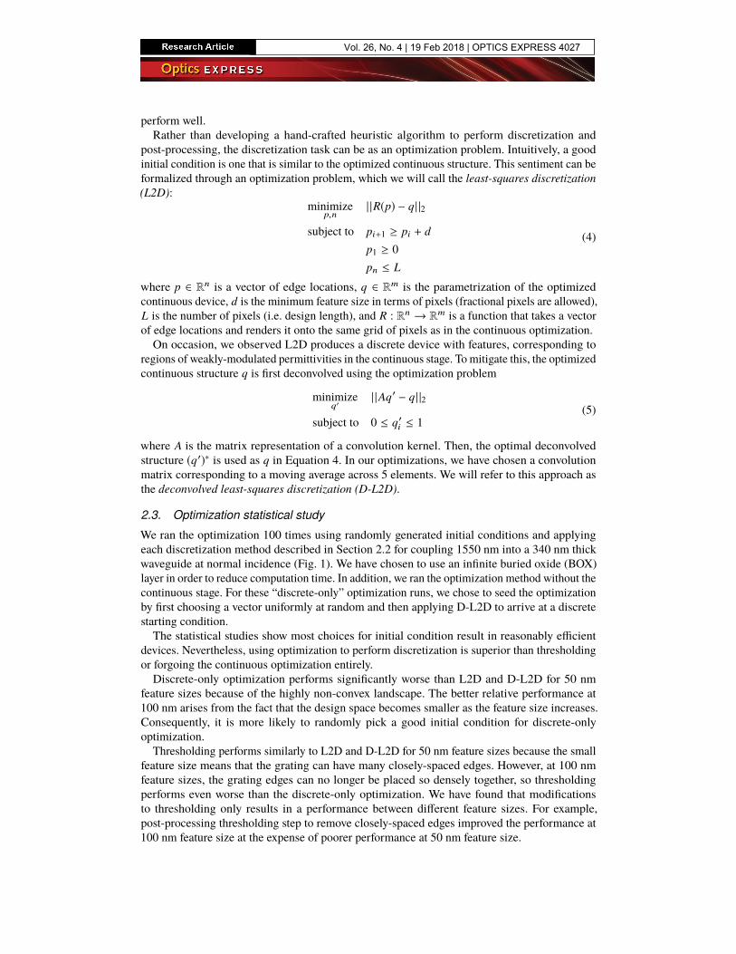
We ran the optimization 100 times using randomly generated initial conditions and applyingeach discretization method described in Section 2.2 for coupling 1550 nm into a 340 nm thickwaveguide at normal incidence (Fig. 1). We have chosen to use an infinite buried oxide (BOX)layer in order to reduce computation time. In addition, we ran the optimization method without thecontinuous stage. For these “discrete-only” optimization runs, we chose to seed the optimizationby first choosing a vector uniformly at random and then applying D-L2D to arrive at a discretestarting condition.The statistical studies show most choices for initial condition result in reasonably efficient
devices. Nevertheless, using optimization to perform discretization is superior than thresholdingor forgoing the continuous optimization entirely.Discrete-only optimization performs significantly worse than L2D and D-L2D for 50 nm
feature sizes because of the highly non-convex landscape. The better relative performance at100 nm arises from the fact that the design space becomes smaller as the feature size increases.Consequently, it is more likely to randomly pick a good initial condition for discrete-onlyoptimization.
Thresholding performs similarly to L2D and D-L2D for 50 nm feature sizes because the smallfeature size means that the grating can have many closely-spaced edges. However, at 100 nmfeature sizes, the grating edges can no longer be placed so densely together, so thresholdingperforms even worse than the discrete-only optimization. We have found that modificationsto thresholding only results in a performance between different feature sizes. For example,post-processing thresholding step to remove closely-spaced edges improved the performance at100 nm feature size at the expense of poorer performance at 50 nm feature size.
Vol. 26, No. 4 | 19 Feb 2018 | OPTICS EXPRESS 4027
50 nm feature size 100 nm feature size
a) b)
c)
Fig. 1. a) Schematic of a typical optimized grating used in the study. b) Close-up schematic ofthe device. c) Distribution of efficiencies for 100 optimization runs for different discretizationprocedures for 50 nm and 100 nm feature sizes. Each optimization run ran for a maximumof 400 iterations (100 for continuous stage and 300 for discrete stage). The orange showsthe distribution of efficiencies achieved at the end of the continuous stage while the blueshows the distribution at the end of the discrete stage. Notice that forgoing the continuousoptimization step leads to worse-performing devices.
Vol. 26, No. 4 | 19 Feb 2018 | OPTICS EXPRESS 4028
In contrast, L2D and D-L2D perform the best in both cases. D-L2D performs slightly betterthan L2D in all cases, both in terms of the mean efficiency and the maximum efficiency out of all100 runs. This is intuitive because L2D performs well when the optimized continuous structureappears mostly discrete, and the deconvolution used in D-L2D does not affect substantiallycontinuous structures that are mostly discrete. Therefore, there is little disadvantage in employingD-L2D over L2D. We have also performed a similar study for wavelength-demultiplexing gratingcouplers and found similar results.
3. Grating coupler designs
In this section, we illustrate our optimization method by designing a wide variety of gratingcouplers, including polarization-insensitive and wavelength-demultiplexing gratings.
3.1. Single-function grating couplers
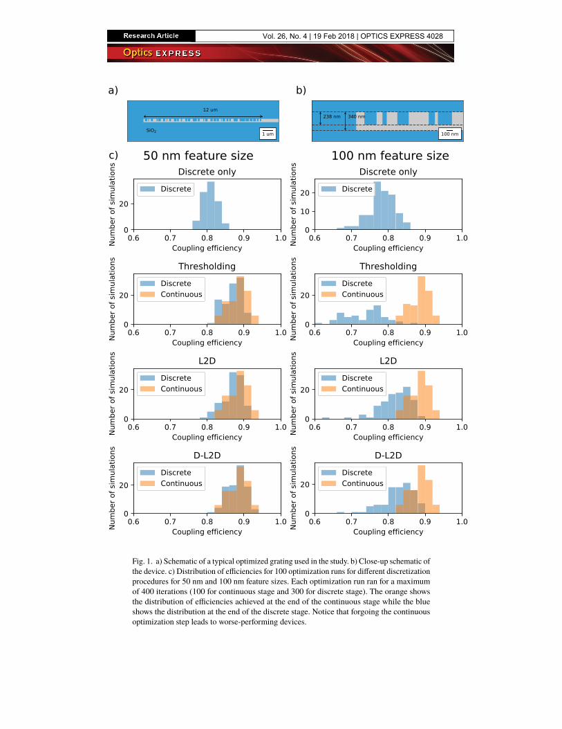
Here we focus on gratings for 1550 nm on the 220 nm thick silicon-on-insulator (SOI) platform.Higher efficiencies can be achieved by using thicker waveguides, but we focus on 220 nm becauseof its role as a common industry standards [1].
14 um
2 umSiO2
Si
SiO2
a)
1 um
220 nm100 nm
b)
100 nm
c)
1520 1530 1540 1550 1560 1570 1580Wavelength (nm)
5
4
3
2
1
0
Eff
icie
ncy
(dB)
Fig. 2. Grating coupler design for 220 nm SOI platform. The angle of incidence is at 10◦from the normal. a) The grating coupler design. The minimum feature size is 100 nm. b)Close-up schematic of the design. c) Simulated coupling efficiency spectrum. The minimuminsertion loss is 1.94 dB, and the 1-dB bandwidth is 34 nm.
Figure 2 shows the design of a conventional grating coupler for 220 nm SOI platform at 10degree incident angle with 100 nm feature sizes. According to analytical theory, the maximumefficiency is achieved by modulating the etch depth or grating period [36]. Ideally, the gratingperiod would become smaller and smaller as one approaches the start of the waveguide. This isprecisely what occurs in our design. At the beginning of the waveguide, the grating periodicity
Vol. 26, No. 4 | 19 Feb 2018 | OPTICS EXPRESS 4029
becomes atypical, but this is a consequence of the desired periodicity falling below the minimumfeature size. This apodized design closely resembles previous optimization work in gratingcouplers [3], and we achieve a similar insertion loss of 1.94 dB (compared to 2.12 dB in [3]).
12 um
SiO2
a)
1 um
220 nm100 nm
b)
100 nm
c)
1520 1530 1540 1550 1560 1570 1580Wavelength (nm)
5
4
3
2
1
0
Eff
icie
ncy
(dB)
Fig. 3. Grating coupler design for 220 nm SOI platform. The device is designed for normalincidence operation. a) The grating coupler design. The minimum feature size is 65 nm. b)Close-up schematic of the design. c) Simulated coupling efficiency spectrum. The minimuminsertion loss is 0.25 dB, and the 1-dB bandwidth is 22 nm.
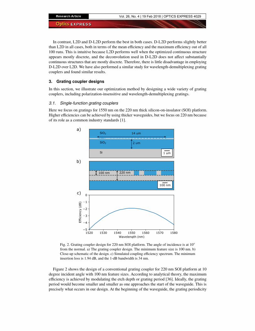
In order to achieve higher efficiencies, one can use more complicated geometries. Figure 3shows a two-layer grating structure optimized with our algorithm. This geometry is similar to theone presented in [10], and we achieve a similar insertion loss of 0.25 dB (compared to 0.165 dB)with a structure that resembles the one presented in [10]. However, in [10], the initial conditionwas physically-motivated by considering constructive and destructive interference between thetop and bottom layers, whereas our algorithm used a completely random initial condition.
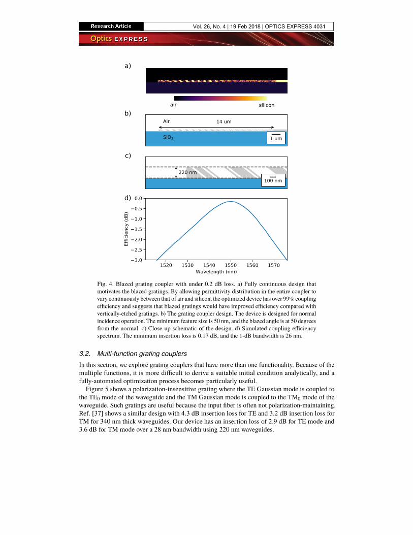
Instead of pre-selecting a particular geometry to optimize, we utilized our method to suggest anoptimal geometry for a single-wavelength grating coupler (Fig. 4). To achieve this, the structurewas parametrized so that all pixels in the design region are allowed to vary continuously. Theoptimized continuous result clearly suggests that blazed gratings are an optimal geometry, whichis consistent with theoretical analysis in [15]. Using this suggestion, we designed a blazed gratingwith 50 degree slant. In order to handle the slants, the continuous stage optimization was modifiedso that each value in the parametrization corresponds to a parallelogram pixel with a width andheight equal to the spatial discretization. The resulting device has a minimum insertion loss of0.17 dB with a 26 nm 1-dB bandwidth.
Vol. 26, No. 4 | 19 Feb 2018 | OPTICS EXPRESS 4030
air silicon
Fig. 4. Blazed grating coupler with under 0.2 dB loss. a) Fully continuous design thatmotivates the blazed gratings. By allowing permittivity distribution in the entire coupler tovary continuously between that of air and silicon, the optimized device has over 99% couplingefficiency and suggests that blazed gratings would have improved efficiency compared withvertically-etched gratings. b) The grating coupler design. The device is designed for normalincidence operation. The minimum feature size is 50 nm, and the blazed angle is at 50 degreesfrom the normal. c) Close-up schematic of the design. d) Simulated coupling efficiencyspectrum. The minimum insertion loss is 0.17 dB, and the 1-dB bandwidth is 26 nm.
3.2. Multi-function grating couplers
In this section, we explore grating couplers that have more than one functionality. Because of themultiple functions, it is more difficult to derive a suitable initial condition analytically, and afully-automated optimization process becomes particularly useful.Figure 5 shows a polarization-insensitive grating where the TE Gaussian mode is coupled to
the TE0 mode of the waveguide and the TM Gaussian mode is coupled to the TM0 mode of thewaveguide. Such gratings are useful because the input fiber is often not polarization-maintaining.Ref. [37] shows a similar design with 4.3 dB insertion loss for TE and 3.2 dB insertion loss forTM for 340 nm thick waveguides. Our device has an insertion loss of 2.9 dB for TE mode and3.6 dB for TM mode over a 28 nm bandwidth using 220 nm waveguides.
Vol. 26, No. 4 | 19 Feb 2018 | OPTICS EXPRESS 4031

a)14 um
2 umSiO2
Si
SiO2
1 um
b)
220 nm100 nm
100 nm
c)
1520 1540 1560 1580Wavelength (nm)
10.0
7.5
5.0
2.5
0.0
Effic
iency
(dB) TE
TM
Fig. 5. Polarization-insensitive grating coupler design for 220 nm SOI platform. The TEGaussian mode is coupled to the TE0 mode of the waveguide and the TM Gaussian mode iscoupled to the TM0 mode of the waveguide. The device is designed for normal incidenceoperation. a) The grating coupler design. The minimum feature size is 50 nm. b) Close-upschematic of the design. c) Simulated coupling efficiency spectrum. The minimum insertionloss is 2.9 dB for TE mode and 3.6 dB for TM mode. The 1-dB bandwidth is 28 nm for bothmodes.
12 um
SiO2
Aira)
1 um
340 nm180 nm
b)
100 nm
c)
1300 1350 1400 1450 1500Wavelength (nm)
8
6
4
2
0
Effic
iency
(dB)
Port 1Port 2
Fig. 6. Wavelength-demultiplexing grating coupler that sends 1310 nm into the left waveguideand 1490 nm into the right waveguide. The device is designed for normal incidence operation.a) The grating coupler design. The minimum feature size is 50 nm. b) Close-up schematic ofthe design. c) Simulated coupling efficiency spectrum. The minimum insertion loss is 1.5dB at 1310 nm and 1.6 dB at 1490 nm with over 21 dB crosstalk suppression. The 1-dBbandwidth is 20 nm at 1310 nm and 24 nm at 1490 nm.
Vol. 26, No. 4 | 19 Feb 2018 | OPTICS EXPRESS 4032

a)
12 um
2 umSiO2
Si
SiO2
1 um
b)
260 nm140 nm
100 nm
c)
1 um
d)
1 um
e)
1300 1350 1400 1450 1500Wavelength (nm)
7.5
5.0
2.5
0.0
Eff
icie
ncy
(dB)
Port 1Port 2
f)
Fig. 7. Wavelength-demultiplexing grating coupler that splits 1310 nm and 1490 nm in thepass-through configuration. The device is designed for normal incidence operation. a) Thepass-through grating coupler geometry used as an optical transceiver. The transmitting laser(blue) couples through an on-chip waveguide to the fiber whereas the receiving wavelength(red) passes through the grating and is detected with a photodetector. b) The grating couplerdesign. c) Close-up schematic of the design. The minimum feature size is 50 nm. d) Realpart of the TE mode electric field at 1310 nm. e) Real part of the TE mode electric field at1490 nm. f) Simulated coupling efficiency spectrum. The minimum insertion loss is 1.0 dBat 1310 nm and 0.08 dB at 1490 nm. The 1-dB bandwidth is 28 nm at 1310 nm.
Next, we designed a wavelength demultiplexing grating coupler that couple 1310 nm light intothe fundamental mode of one waveguide and couple 1490 nm light into the fundamental mode ofanother waveguide (Fig. 6). Such a grating is useful in wavelength division multiplexing systemswhere multiple wavelengths are utilized to increase the communication bandwidth. Unlike [38]and [39], this grating operates at normal incidence. This is a geometry that we have studied beforein [40] but the design presented there was a focused Gaussian spot rather than one meant for fibermode. The device presented here has an insertion loss of 1.5 dB at 1310 nm and 1.6 dB at 1490nm with over 21 dB crosstalk suppression. We note that this was achieved using an infinite BOXlayer, which is a more difficult design problem.To achieve even higher efficiency for wavelength demultiplexing designs, we introduce the
pass-through geometry in which only one of the wavelengths is coupled into an on-chip waveguidewhereas another wavelength passes through the grating. A photodetector can then be placedbehind the chip to collect the light that passes through the device. This is useful for systems wherethe pass-through wavelength does not require additional processing. One particular applicationis in an optical transceiver: The transmitting wavelength would out-couple into an optical fiberthrough the waveguide whereas the receiving wavelength would pass through the structure and bedetected (Fig. 7(a)). The advantage of this geometry is that the the couplers can be more efficientbecause high transmission through the grating is easier to achieve. Figure 7 shows a design with1.0 dB insertion loss at 1310 nm (the on-chip wavelength) and 0.08 dB loss at 1490 nm (thepass-through wavelength).
Vol. 26, No. 4 | 19 Feb 2018 | OPTICS EXPRESS 4033
4. Conclusion
We have presented a general gradient-based 1D grating design algorithm that fully automatesthe design process, enabled by appropriately choosing a least-squares discretization procedure.Using this algorithm, we design efficient couplers in different geometries and with differentfunctionalities, including polarization-insensitive gratings, wavelength-demultiplexing gratings,and a single-wavelength grating coupler with under 0.2 dB insertion loss.
Funding
Air Force Office of Scientific Research (AFOSR) MURI for Aperiodic Silicon Photonics(FA9550-15-1-0335); Gordon and Betty Moore Foundation; Futurewei Technologies, Inc.; MarieSklodowska-Curie Grant (665501); Kailath Stanford Graduate Fellowship.
Acknowledgements
D. V. acknowledges funding from FWO and European Union’s Horizon 2020 research andinnovation program under the Marie Sklodowska-Curie grant agreement No 665501. We thankGoogle for providing computational resources on the Google Cloud Platform.
Vol. 26, No. 4 | 19 Feb 2018 | OPTICS EXPRESS 4034