Embed Size (px)
Citation preview

Copyright © Future Technology Devices International Limited 1
FT602Q IC Datasheet
Version 1.3
Document No.: FT001389 Clearance No.: FTDI#519
Future Technology
Devices International Ltd.
FT602Q IC Datasheet
(FIFO to USB 3.0 UVC Bridge)
The FT602 is a USB-to-FIFO interface to SuperSpeed USB (USB 3.1 Gen 1) USB Video Class (UVC) bridge chip with the following advanced features:
Supports USB 3.1 GEN 1 Super Speed
(5Gbps) / USB 2.0 High Speed (480Mbps)
Supports USB Transfer Types: Control/Bulk/Interrupt
Supports UVC version 1.1
Supports up to 4 video input channels on the FIFO bus.
Supports 2 parallel slave FIFO bus protocols,
245 FIFO and Multi-channel FIFO mode, with a data burst rate up to 400MB/s with 32 bit
parallel interface
Built-in 16kB FIFO data buffer RAM.
Built-in I2C master interface for video device configuration
Supports multi voltage I/O: 1.8V, 2.5V and 3.3V.
Internal LDO 1.0V regulator.
Integrated power-on-reset circuit.
User programmable USB and UVC descriptors.
Industrial operating temperature range: -40 to 85⁰C.
Available in compact Pb-free QFN-76 RoHS compliant package.
Neither the whole nor any part of the information contained in, or the product described in this manual, may be adapted or reproduced in any material or electronic form without the prior written consent of the copyright holder. This product and its documentation are
supplied on an as-is basis and no warranty as to their suitability for any particular purpose is either made or implied. Future Technology
Devices International Ltd will not accept any claim for damages howsoever arising as a result of use or failure of this product. Your
statutory rights are not affected. This product or any variant of it is not intended for use in any medical appliance, device or system in
which the failure of the product might reasonably be expected to result in personal injury. This document provides preliminary
information that may be subject to change without notice. No freedom to use patents or other intellectual property rights is implied by
the publication of this document. Future Technology Devices International Ltd, Unit 1, 2 Seaward Place, Centurion Business Park,
Glasgow G41 1HH United Kingdom. Scotland Registered Company Number: SC136640
Copyright © Future Technology Devices International Limited 2
FT602Q IC Datasheet
Version 1.3
Document No.: FT001389 Clearance No.: FTDI#519
1 Typical Applications
USB 3.1 Digital Video Camera Interface
USB 3.1 Digital Camera
Medical/Industrial imaging devices
USB 3.1 Instrumentation
1.1 Driver Support
USB Video Class Driver
Windows 10
Windows 8.1
Windows 7
Mac OS-X
Linux
1.2 Ordering Information
Part Number Package
FT602Q-B-x 76 Pin QFN 0.4mm Pitch, body 9mm x 9mm x 0.9mm
Table 1.1 Device Part Numbers
Note: Packaging codes for x is: -R: Taped and Reel, (VQFN in 3000 pieces per reel)
-T: Tray packing, (VQFN in 260 pieces per tray) For example: FT602Q-B-R is 3000 QFN pieces in taped and reel packaging
1.3 USB Compliance
The FT602Q is compliant with the USB 3.1 Gen 1 specification. Please contact us for further details on USB compliance.

Copyright © Future Technology Devices International Limited 3
FT602Q IC Datasheet
Version 1.3
Document No.: FT001389 Clearance No.: FTDI#519
2 Block Diagram
Figure 2.1 Block Diagram
For a description of each function please refer to Section 4.

Copyright © Future Technology Devices International Limited 4
FT602Q IC Datasheet
Version 1.3
Document No.: FT001389 Clearance No.: FTDI#519
Table of Contents
1 Typical Applications ............................................................ 2
1.1 Driver Support ................................................................................ 2
1.2 Ordering Information ...................................................................... 2
1.3 USB Compliance .............................................................................. 2
2 Block Diagram .................................................................... 3
3 Device Pin Out and Signal Description ................................ 6
3.1 Device Pin Out ................................................................................ 6
3.2 Device Pin Out Signal Description ................................................... 6
4 Function Description ........................................................ 10
4.1 Key Features and Function Description ......................................... 10
4.2 Multi-Channel FIFO mode Protocols .............................................. 11
4.3 245 Synchronous FIFO mode Protocols ......................................... 13
4.4 FIFO Bus AC Timing ...................................................................... 13
4.5 Crystal Requirements .................................................................... 14
4.6 I2C Interface ................................................................................. 14
5 Devices Characteristics and Ratings ................................. 15
5.1 Absolute Maximum Ratings ........................................................... 15
5.2 ESD and Latch-up Specifications ................................................... 15
5.3 DC Characteristics ......................................................................... 16
5.3.1 DC Characteristics (Ambient Temperature = -40°C to +85°C) ........................... 16
5.3.2 DC Characteristics for I/O Interface ................................................................ 17
6 USB Power Configurations ................................................ 18
6.1 USB Bus-Powered Configuration .................................................. 18
6.2 Self-Powered Configuration .......................................................... 19
7 Application Example ......................................................... 20
7.1 FT602 Connect to FIFO Master Interface ...................................... 20
8 Package Parameters ......................................................... 22
8.1 QFN-76 Package Mechanical Dimensions ...................................... 22
8.2 QFN-76 Package Markings ............................................................ 23
8.3 Solder Reflow Profile .................................................................... 24

Copyright © Future Technology Devices International Limited 5
FT602Q IC Datasheet
Version 1.3
Document No.: FT001389 Clearance No.: FTDI#519
9 Contact Information ......................................................... 25
Appendix A – References ........................................................ 26
Document References ........................................................................... 26
Acronyms and Abbreviations ................................................................. 26
Appendix B – List of Figures and Tables .................................. 27
List of Figures ....................................................................................... 27
List of Tables ......................................................................................... 27
Appendix C – Revision History ................................................ 28

Copyright © Future Technology Devices International Limited 6
FT602Q IC Datasheet
Version 1.3
Document No.: FT001389 Clearance No.: FTDI#519
3 Device Pin Out and Signal Description
3.1 Device Pin Out
Figure 3.1 FT602 Pin Out
3.2 Device Pin Out Signal Description
Pin Name Description Type Pin No.
CLK
Parallel FIFO bus clock output pin to the FIFO bus master. The Frequency can be configured as 66Mhz or 100Mhz for both FIFO bus modes.
O 58
DATA_0 Parallel FIFO bus data input bit 0. I 40
DATA_1 Parallel FIFO bus data input bit 1. I 41
DATA_2 Parallel FIFO bus data input bit 2. I 42

Copyright © Future Technology Devices International Limited 7
FT602Q IC Datasheet
Version 1.3
Document No.: FT001389 Clearance No.: FTDI#519
DATA_3 Parallel FIFO bus data input bit 3. I 43
DATA_4 Parallel FIFO bus data input bit 4. I 44
DATA_5 Parallel FIFO bus data input bit 5. I 45
DATA_6 Parallel FIFO bus data input bit 6. I 46
DATA_7 Parallel FIFO bus data input bit 7. I 47
DATA_8 Parallel FIFO bus data I/O bit 8. I/O 50
DATA_9 Parallel FIFO bus data I/O bit 9. I/O 51
DATA_10 Parallel FIFO bus data I/O bit 10. I/O 52
DATA_11 Parallel FIFO bus data I/O bit 11. I/O 53
DATA_12 Parallel FIFO bus data I/O bit 12. I/O 54
DATA_13 Parallel FIFO bus data I/O bit 13. I/O 55
DATA_14 Parallel FIFO bus data I/O bit 14. I/O 56
DATA_15 Parallel FIFO bus data I/O bit 15. I/O 57
DATA_16 Parallel FIFO bus data input bit 16. I 60
DATA_17 Parallel FIFO bus data input bit 17. I 61
DATA_18 Parallel FIFO bus data input bit 18. I 62
DATA_19 Parallel FIFO bus data input bit 19. I 63
DATA_20 Parallel FIFO bus data input bit 20. I 64
DATA_21 Parallel FIFO bus data input bit 21. I 65
DATA_22 Parallel FIFO bus data input bit 22. I 66
DATA_23 Parallel FIFO bus data input bit 23. I 67
DATA_24 Parallel FIFO bus data input bit 24. I 69
DATA_25 Parallel FIFO bus data input bit 25. I 70
DATA_26 Parallel FIFO bus data input bit 26. I 71
DATA_27 Parallel FIFO bus data input bit 27. I 72
DATA_28 Parallel FIFO bus data input bit 28. I 73
DATA_29 Parallel FIFO bus data input bit 29. I 74
DATA_30 Parallel FIFO bus data input bit 30. I 75
DATA_31 Parallel FIFO bus data input bit 31. I 76

Copyright © Future Technology Devices International Limited 8
FT602Q IC Datasheet
Version 1.3
Document No.: FT001389 Clearance No.: FTDI#519
BE_0 Parallel FIFO bus byte enable I/O bit 0. I/O 4
BE_1 Parallel FIFO bus byte enable I/O bit 1. I/O 5
BE_2 Parallel FIFO bus byte enable I/O bit 2. I/O 6
BE_3 Parallel FIFO bus byte enable I/O bit 3. I/O 7
TXE_N
245 Synchronous FIFO mode: Transmit FIFO Empty output signal. The signal indicates there is a minimum of 1 byte of space available to write to. Only write to the FIFO when this signal is logic 0.
Multi-Channel FIFO mode: Status Valid output signal (optional).
O
8
RXF_N
245 Synchronous FIFO mode: Add external pull up in normal operation.
Multi-Channel FIFO mode: Data Receive Acknowledge output signal.
O
9
RESERVED1 Reserved. Add external pull up in normal operation. I 10
WR_N
245 Synchronous FIFO mode: Write Enable input signal.
Multi-Channel FIFO mode: Data Transaction Request input signal.
The signal is active low.
I
11
RESERVED2 Add external pull up in normal operation. I 12
RESERVED3 Add external pull up in normal operation. I 13
RESET_N Chip Reset input, Active low. I 15
INT_N Interrupt input pin, active low. I 16
RESERVED4 Reserved. Do not connect. NC 19
SCL I2C Serial Clock line OD 17
SDA I2C Serial Data line OD 18
VBUS USB BUS power detect pin. The input voltage should be greater than 2.7V.
I 37
XI Crystal input. This terminal is the crystal input for the internal oscillator.
I 21
XO Crystal Output. This terminal is the crystal output for the internal oscillator.
O 22
DP Hi-speed USB differential transceiver (positive) I/O 23
DM Hi-speed USB differential transceiver (negative) I/O 25

Copyright © Future Technology Devices International Limited 9
FT602Q IC Datasheet
Version 1.3
Document No.: FT001389 Clearance No.: FTDI#519
RREF
PHY reference resistor input pin. Connect 1.6k Ω 1% resistor to ground, provides reference voltage to USB2 PHY.
I 27
TODN Super Speed USB transmitter differential pair (negative) O 31
TODP Super Speed USB transmitter differential pair (positive) O 32
RIDN Super Speed USB receiver differential pair (negative) I 34
RIDP Super Speed USB receiver differential pair (positive) I 35
VCC33 +3.3V power input for chip and internal LDO. PWR
20,24,38
DV10
+1.0V power output from internal LDO. Connecting to VD10 and AVDD, with a 4.7uF cap to ground is
recommended.
O
39
VD10 +1.0V core voltage input. PWR
3,30,33,48
VCCIO Power input for I/O block, supports +2.5/+3.3V. PWR
14,49,59,68
VDDA +3.3V power input for USB2.0 and USB3.0 PHYs. PWR 28
AVDD +1.0V power input for PLL. PWR 2
GND Ground GND
1,26,
29,36
Table 3.1 Device pinout signal descriptions

Copyright © Future Technology Devices International Limited 10
FT602Q IC Datasheet
Version 1.3
Document No.: FT001389 Clearance No.: FTDI#519
4 Function Description
The FT602 is a high performance USB 3.1 UVC bridge with a FIFO interface. It is designed to transfer uncompressed YUV422 video data from the 32bit FIFO interface to the USB 3.1 bus. It supports resolutions
and frame rates up to 1920x1080@60 frames per second. In FT600 multi-channel mode, up to 4 UVC channels of video may be transported. It can be used in those applications which require high resolution imaging devices. The FIFO interface supports multi-voltage I/O of 1.8V, 2.5V or 3.3V and operating frequencies of 66MHz or 100MHz. At 100MHz operation only 2.5V or 3.3V I/O voltages are supported.
There are 2 different proprietary synchronous bus protocols supported; one FIFO bus protocol is called the “Multi-Channel FIFO” bus protocol, also known as the FT600 FIFO protocol and the other is the “245 Synchronous FIFO” bus protocol. The latter being an extension of the interface introduced in the FT232H/FT2232H devices. *FIFO bus data lines are driven by the FIFO master, the FT602 only reads data from the FIFO master.
4.1 Key Features and Function Description
Functional Integration
The following features are integral to the IC design: FIFO protocol management, USB 3.1 (Gen 1) controller, USB3.0 and USB2.0 PHYs, power management, clock generation, power-on-reset (POR) and LDO regulator.
USB 3.1 Protocol Controller
The USB 3.1 Protocol Controller manages the data stream from the device USB control endpoint. It handles the USB protocol requests generated by the USB host controller and the commands for controlling the
functional parameters of the endpoint in accordance with the USB 3.1 specification. 32KB of burst buffers are available in the protocol controller. These buffers are allocated to the UVC channels according to the required video bandwidth. The factory programmed default is for a single UVC channel and all burst buffers are allocated to the single channel. The default configuration may be customised by using the FT602 Chip
Configuration utility.
FIFO Management
This unit is used to manage all PIPE data or buffers in the FIFO memory; the data is sent or received through the FIFO protocol layer. Through this block the FIFO memory can be allocated to each PIPE with any size of memory as long as the total memory allocated to all PIPEs does not exceed the maximum FIFO memory size which is 16KB. Additionally, the FIFO signals have a configurable high drive strength capability and can be set to 18Ω, 25Ω, 35Ω and 50Ω.
Multi-Channel FIFO Bus protocol
The multi-Channel FIFO bus is a slave bus and is designed to handle Multi-Channel FIFO connectivity. The bus protocol supports a total of 4 IN channels. CLK is the clock output to the FIFO bus master.
245 Synchronous FIFO Bus protocol
The 245 Synchronous FIFO bus is a slave bus with one IN FIFO channel supported by this bus protocol. CLK is the clock output to the FIFO bus master.
FIFO Bus Clock Option
The device provides the following FIFO bus clock frequency option: 66MHz, 100MHz.

Copyright © Future Technology Devices International Limited 11
FT602Q IC Datasheet
Version 1.3
Document No.: FT001389 Clearance No.: FTDI#519
FIFO Buffer (16K bytes)
Data written into the FIFO is stored in the FIFO buffer and transferred to the USB endpoint buffers and prepared for transmission to the USB host. The data is transferred to the host whenever the IN endpoint is ready to receive data.
The FIFO and EPC burst buffers in the FT602 may be configured to correspond to the required throughput of the UVC channel. The factory programmed default configuration is for a single UVC channel with the entire 16KB FIFO buffer allocated to the single IN channel. The default configuration may be customised by using the FT602 Chip Configuration utility.
Internal LDO Regulator
The LDO regulator generates the +1.0V power supply for driving the internal core of the device. This supply is not to be used for external devices and is meant for decoupling.
Reset Generator
The integrated Reset Generator module provides a reliable power-on reset to the device internal circuitry at power up. The RESET_N input pin allows an external device to reset the FT602. This pin is an active low input.
Interrupt
One interrupt pin is provided; this pin can be used for I2C interrupt request or to wake up the FT602 device from sleep mode.
I2C bus
The FT602 provides an I2C bus which operates as master, the transmission speed defaults to 800 Kb/s.
USB Video Class Device
The UVC device has configurations for SuperSpeed, Hi-speed, and full speed devices. The device is compliant to UVC Version 1.1 and supports the following features.
Up to 14 customisable resolutions each in FS, HS, SS modes, up to UHD.
Up to 4 UVC sources simultaneously.
Up to 60fps of F-HD input.
4.2 Multi-Channel FIFO mode Protocols
The FIFO interface is a slave bus and is designed to handle multi-channel connectivity. The bus protocol supports a total of 4 IN channels; each has a corresponding USB IN endpoint. CLK is the clock output from the bus slave to the bus master. The channel numbers denoted in this document as channels 1 to 4 are mapped to USB endpoint numbers 1 to 4. The USB IN endpoint in Channel 1 is denoted as USB IN channel 1.
Correspondingly, the FIFO IN is for data transmitted from the USB device to the host.
WR_N is the bus master to bus slave data transaction request signal, and it is active low. RXF_N is the bus slave to bus master data receive acknowledge signal, and it is active low.
TXE_N (optional signal, the master can ignore this signal) is the bus slave to bus master FIFO idle status valid signal, and it is active low. DATA[31:0] is used as the 32-bit data bus during the data transfer phase. When the bus is in the idle state DATA[31:16], DATA[7:0] and BE[3:0] are driven to logic”1” by the bus master, and DATA[15:8] is driven by the bus slave to provide the FIFO status to the bus master. The lower nibble (DATA[11:8]) provides the 4 IN
channels FIFO status. They are all active low.

Copyright © Future Technology Devices International Limited 12
FT602Q IC Datasheet
Version 1.3
Document No.: FT001389 Clearance No.: FTDI#519
For example, at idle, DATA[8] is logic”0”, which indicates USB IN channel 1 FIFO space is empty and able to receive data . The external bus master will start a transfer cycle by asserting WR_N based on the channel FIFO status. The first cycle after WR_N is asserted is the command phase, followed by the data phase when RXF_N is asserted. At the command phase, the bus master will send the channel number which it intends to transfer data with on DATA[7:0] and the Write command on BE[3:0]. BE[3:0] = ‘h1 indicates a master write.
There may also be a required turn-a-round for DATA[31:0] and BE[3:0] after the command phase and at the end of data transaction.
Table 4.1 shows Multi-Channel FIFO mode command phase master write and channel address setting.
Command Phase FT602 Command BE[3:0]
Channel Address DATA[7:0]
Master Write
0001
8’h1=Channel 1
8’h2=Channel 2
8’h3=Channel 3
8’h4=Channel 4
All other values are reserved and shall be ignored
Table 4.1 Multi-Channel FIFO mode Command phase Note: The channels can be configured by using the FT602 Chip Configuration utility.
The waveform below shows a FT602 master write transaction for 14 bytes at channel 1 with the bus master terminating the transaction. There are turn-a-round cycles for DATA[15:8] after the command phase and at the end of the data transaction. The BE[3:0] shows that the lower 2 bytes in D3 are valid at the last word
strobe in this transaction.
Figure 4.1 Multi-Channel FIFO mode master write transaction 1
NOTE: There is no turnaround phase for BE pins as these remain inputs when the FIFO is being written to by the master.
The waveform below shows a FT602 master write transaction where the FIFO at channel 1 uses all data space first, the RXF_N reasserts when the FIFO data space is not available after D3. There are turn-a-round cycles
for DATA[15:8] after the command phase and at the end of the data transaction. The BE[3:0] shows that the transaction is all word aligned, all 4 bytes in D3 are valid at the last word strobe in this transaction.

Copyright © Future Technology Devices International Limited 13
FT602Q IC Datasheet
Version 1.3
Document No.: FT001389 Clearance No.: FTDI#519
Figure 4.2 Multi-Channel FIFO mode master write transaction 2
4.3 245 Synchronous FIFO mode Protocols
This FT602 slave FIFO bus uses one IN FIFO channel while in this mode. CLK is the clock output to the bus master; it can be configured as 66 MHz or 100 MHz TXE_N is an output signal, Transmit FIFO Empty. It is active low and when active it indicates the Transmit
FIFO has space and it is ready to receive data from the FIFO master. WR_N is an input signal, Write Enable. It is active low and when it is driven low by the bus master, the master has write cycle access. BE[3:0] is the byte enable signal. In bus master write operation, the bus master asserts the signal for the valid bytes in a word strobe. Normally, all 4 bytes should be valid in a bus transaction except in the last word
strobe when the data transaction length is not aligned at a word boundary. The waveform below shows 245 synchronous FIFO bus master write cycles.
Figure 4.3 245 Synchronous FIFO mode bus master write cycle
*In 245 Synchronous FIFO mode master write operation, if the bus master expects the data to be transferred on the USB bus in a maximum possible packet length, it should write the data to the FIFO in a single bus
transaction.
4.4 FIFO Bus AC Timing
The FT602 device FIFO bus is a synchronous parallel bus. The CLK signal is generated by the device, with the
typical FIFO clock duty cycle of 50%. Both Multi-Channel and 245 synchronous FIFO modes’ worst case AC timing are shown in Figure 4.8 and Table 4.2. In this figure, ‘Input Data’ includes all control signals and data lines driven by the FIFO master. ‘Output Data’ includes all control signals driven by the FIFO slave - FT602.
CLK
Copyright © Future Technology Devices International Limited 14
FT602Q IC Datasheet
Version 1.3
Document No.: FT001389 Clearance No.: FTDI#519
Figure 4.4 FIFO Bus AC timing diagram
Time Description Minimum Maximum Unit
T1 Slave Drive Data Set Up Time 3.0 - ns
T2 Slave Drive Data Hold Time 3.5 - ns
T3 Master Drive Data Set Up Time 1 - ns
T4 Master Drive Date Hold Time 4.8 - ns
Table 4.2 FIFO Bus AC timing
4.5 Crystal Requirements
The FT602 device requires an external clock source to control the internal circuitry.
The recommended parameters for the crystal are: 30MHz ±20ppm Crystal 18pF 50 Ohm -40°C ~ 85°C. The crystal should be connected across the XI and XO pins. Note: Replacing the crystal with an oscillator or other clock source by tying XO to GND is not supported
4.6 I2C Interface
The I2C master supports 3 operating frequencies, 800 kHz, 400 kHz and 100 kHz. The frequency may be set through the FT602 configuration utility. The I2C master issues repeated start for read operations and it does not support arbitration and clock stretching.
I2C commands are issued by FT602 under the following conditions:
1. FT602 defined commands to convey video resolution selection and start of streaming
2. UVC command (camera and processing unit) pass through to I2C slave device
3. Side-band pass through (opaque data) by user supplied host application via configuration interface. Slave device initiated communication can be retrieved
AN_434_FT602_UVC_Bus_Master_Sample describes the I2C slave register map.
Output Data
T1
Input Data
T2
T3
T4

Copyright © Future Technology Devices International Limited 15
FT602Q IC Datasheet
Version 1.3
Document No.: FT001389 Clearance No.: FTDI#519
5 Devices Characteristics and Ratings
5.1 Absolute Maximum Ratings
The absolute maximum ratings for the FT602 devices are as follows. These are in accordance with the Absolute Maximum Rating System (IEC 60134). Exceeding these may cause permanent damage to the device.
Parameter Value Unit
Storage Temperature -65°C to 150°C Degrees C
Ambient Operating Temperature (Power Applied) -40°C to 85°C Degrees C
VCC33/VDDA Supply Voltage -0.3 to +4.6 V
VCCIO Supply Voltage -0.3 to +4.0 V
VD10 Core Supply Voltage -0.5 to +1.4 V
AVDD PLL Supply Voltage -0.5 to +1.4 V
IOs DC Input Voltage -0.5 to +VCCIO+0.5 V
Table 5.1 Absolute Maximum Ratings
5.2 ESD and Latch-up Specifications
Description Reference Min Typical Max Units
Human Body Mode
(HBM) JEDEC EIA/JESD22- A114-
B, Class 2
- ±2kV - kV
Machine mode
(MM)
JEDEC EIA/JESD22- A115-A, Class B
- ±200V - V
Charged Device
Mode (CDM) JEDEC EIA/ JESD22-C101-
D, Class-III
- ±500V - V
Latch-up JESD78, Trigger Class-II - ±200mA - mA
Table 5.2 ESD and Latch-Up Specifications

Copyright © Future Technology Devices International Limited 16
FT602Q IC Datasheet
Version 1.3
Document No.: FT001389 Clearance No.: FTDI#519
5.3 DC Characteristics
5.3.1 DC Characteristics (Ambient Temperature = -40°C to +85°C)
Parameter Description Min Typical Max Units Conditions
VCC33/VDDA VCC Operating Supply
Voltage 3.0 3.3 3.6 V
VCCIO_1 VCCIO Operating Supply Voltage
3.0 3.3 3.6 V VCCIO=3.3V
VCCIO_2 VCCIO Operating Supply Voltage
2.3 2.5 2.7 V VCCIO=2.5V
VCCIO_3 VCCIO Operating
Supply Voltage 1.65 1.8 1.95 V VCCIO=1.8V
VD10/AVDD Core/PLL Operating
Supply Voltage 0.9 1.0 1.1 V
Icc_1 VCC Operating Supply
Current - 85 - mA Idle, SuperSpeed
Icc_2 VCC Operating Supply
Current - 69 - mA Idle, High Speed
Icc_3 VCC Operating Supply
Current - 185 - mA
FHD 1080P@60fps Output
Icc_3 VCC Operating Supply
Current - 4 - mA USB Suspend
Iccio_1 VCCIO Operating
Supply Current - 4.5 - mA No data transfer
Iccio_2 VCCIO Operating Supply Current
9.5 mA Data transfer
Iccio_3 VCCIO Operating Supply Current
70 μA USB Suspend
Table 5.3 DC Characteristics

Copyright © Future Technology Devices International Limited 17
FT602Q IC Datasheet
Version 1.3
Document No.: FT001389 Clearance No.: FTDI#519
5.3.2 DC Characteristics for I/O Interface
Parameter Description Min Typical Max Units Conditions
VCCIO_3.3V
VCCIO Operating
Supply Voltage
3.0 3.3 3.6 V Normal Operation
VCCIO_2.5V 2.3 2.5 2.7 V Normal Operation
VCCIO_1.8V 1.65 1.8 1.95 V Normal Operation
VIH VCCIO*0
.7 - - V
Normal Operation
VIL - - VCCIO*0.
3 V
Normal
Operation
Iin/Iout(3.3V) Input/output Leakage -10 - 10 uA Without pull-up/down
Rpu/Rpd Input pull-up/pull down resistance
30 50 75 KΩ Vout=0~ VCCIO
Iout(VCCIO=3.3V) Output drive strength 10 - - mA Total current
Iout(VCCIO=2.5V) Output drive strength 9.4 - - mA Total current
Cp Pin Capacitance - - 2.0 pF
Table 5.4 DC Characteristics for I/O Interface (Except USB PHY pins)

Copyright © Future Technology Devices International Limited 18
FT602Q IC Datasheet
Version 1.3
Document No.: FT001389 Clearance No.: FTDI#519
6 USB Power Configurations
The following sections illustrate possible USB power configurations for the FT602. The illustrations have omitted pin numbers for ease of understanding.
6.1 USB Bus-Powered Configuration
Note: The reference designs here are for USB 3.1 Standard B or Micro-B connectors.
Figure 6.1 Bus-Powered Configuration-1.8V/2.5V I/O Figure 6.1 illustrate the FT602 in a typical USB bus powered design configuration. The FT602 device gets its power(VCC33) from the USB bus via an external LDO(LDO_3V3) stepping the voltage down to +3.3V. Another external LDO stepping the voltage down to +2.5V for supplying the VCCIO power, connect VCCIO pins to
same LDO(LDO_3V3) if VCCIO is configured to 3.3V. A ferrite bead is connected in series with the USB power supply to reduce EMI noise from the FT602 and associated circuitry being radiated down the USB cable to the USB host. The value of the Ferrite Bead depends on the total current drawn by the application.

Copyright © Future Technology Devices International Limited 19
FT602Q IC Datasheet
Version 1.3
Document No.: FT001389 Clearance No.: FTDI#519
6.2 Self-Powered Configuration
Figure 6.2 Self-Powered Configuration
Figure 6.2 illustrates the FT602 in a typical USB self-powered configuration. The FT602 device gets its power from its own power supply, VCC33 and VCCIO, and does not draw current from the USB bus.
The basic rules for USB self-powered devices are as follows –
i) A self-powered device should not force current down the USB bus when the USB host or hub controller
is powered down. ii) A self-powered device can use as much current as it needs during normal operation and USB suspend
as it has its own power supply. iii) A self-powered device can be used with any USB host, a bus powered USB hub or a self-powered USB
hub.

Copyright © Future Technology Devices International Limited 20
FT602Q IC Datasheet
Version 1.3
Document No.: FT001389 Clearance No.: FTDI#519
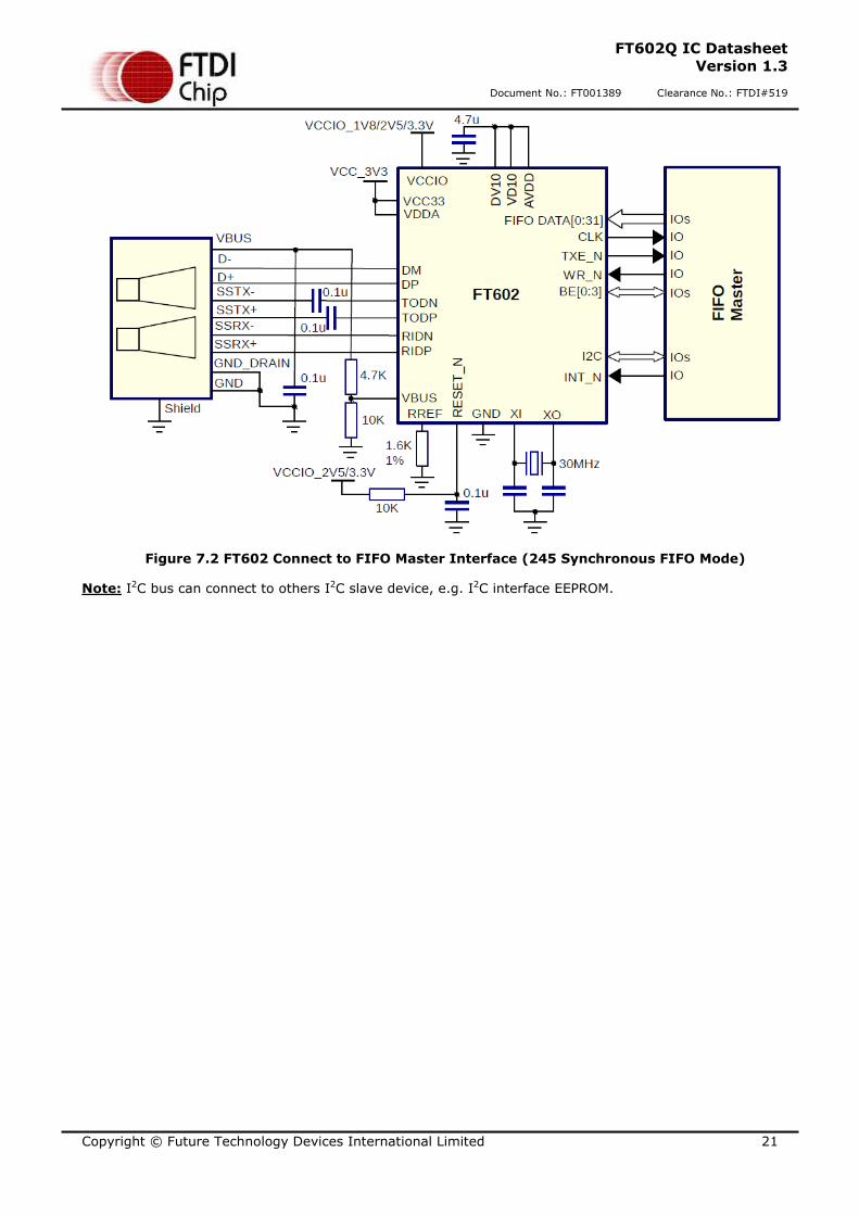
7 Application Example
The following sections illustrate the typical application of the FT602 UVC bridge device. The illustrations have omitted pin numbers for ease of understanding.
A typical example of the FT602 UVC Bridge to FIFO Master Interface is illustrated in Figure 7.1 and Figure 7.2.
7.1 FT602 Connect to FIFO Master Interface
Figure 7.1 FT602 Connect to FIFO Master Interface (Multi-Channel FIFO Mode)
Copyright © Future Technology Devices International Limited 21
FT602Q IC Datasheet
Version 1.3
Document No.: FT001389 Clearance No.: FTDI#519
Figure 7.2 FT602 Connect to FIFO Master Interface (245 Synchronous FIFO Mode)
Note: I2C bus can connect to others I2C slave device, e.g. I2C interface EEPROM.

Copyright © Future Technology Devices International Limited 22
FT602Q IC Datasheet
Version 1.3
Document No.: FT001389 Clearance No.: FTDI#519
8 Package Parameters
The FT602 is available in a QFN-76 package.
8.1 QFN-76 Package Mechanical Dimensions
Figure 8.1 QFN-76 Package Dimensions The FT602Q is supplied in a RoHS compliant leadless QFN-76 package. The package is lead ( Pb ) free, and uses a ‘green’ compound. The package is fully compliant with European Union directive 2002/95/EC.
This package is nominally 9.0mm x 9.0mm body. The solder pads are on a 0.40mm pitch. The above mechanical drawing shows the QFN-76 package. The centre pad on the base of the FT602Q is internally connected to GND, the PCB should connect to ground and not have signal tracking on the same layer as chip in this area.

Copyright © Future Technology Devices International Limited 23
FT602Q IC Datasheet
Version 1.3
Document No.: FT001389 Clearance No.: FTDI#519
8.2 QFN-76 Package Markings
Figure 8.2 QFN-76 Package Markings Notes:
1. YYWW = Date Code, where YY is year and WW is week number
2. Marking alignment should be centre justified
3. Laser Marking should be used
4. All marking dimensions should be marked proportionally. Marking font should be using Greatek
standard font (Roman Simplex)
FTDI
XXXXXXXXXX
FT602Q
Line 1 – FTDI Logo
Line 4 – Date Code, Revision
Line 2 – Wafer Lot Number
1
76
Line 3 – FTDI Part Number
YYWW-B

Copyright © Future Technology Devices International Limited 24
FT602Q IC Datasheet
Version 1.3
Document No.: FT001389 Clearance No.: FTDI#519
8.3 Solder Reflow Profile
Figure 8.3 Solder Reflow Profile

Copyright © Future Technology Devices International Limited 25
FT602Q IC Datasheet
Version 1.3
Document No.: FT001389 Clearance No.: FTDI#519
9 Contact Information
Head Office – Glasgow, UK Branch Office – Tigard, Oregon, USA
Future Technology Devices International Limited Unit 1, 2 Seaward Place, Centurion Business Park Glasgow G41 1HH United Kingdom Tel: +44 (0) 141 429 2777 Fax: +44 (0) 141 429 2758
Future Technology Devices International Limited (USA) 7130 SW Fir Loop Tigard, OR 97223-8160 USA Tel: +1 (503) 547 0988 Fax: +1 (503) 547 0987
E-mail (Sales) [email protected] E-mail (Sales) [email protected] E-mail (Support) [email protected] E-mail (Support) [email protected] E-mail (General Enquiries) [email protected] E-mail (General Enquiries) [email protected]
Branch Office – Taipei, Taiwan Branch Office – Shanghai, China
Future Technology Devices International Limited (Taiwan) 2F, No. 516, Sec. 1, NeiHu Road Taipei 114 Taiwan , R.O.C. Tel: +886 (0) 2 8797 1330 Fax: +886 (0) 2 8751 9737
Future Technology Devices International Limited (China) Room 1103, No. 666 West Huaihai Road, Shanghai, 200052 China Tel: +86 21 62351596 Fax: +86 21 62351595
E-mail (Sales) [email protected] E-mail (Sales) [email protected] E-mail (Support) [email protected] E-mail (Support) [email protected] E-mail (General Enquiries) [email protected] E-mail (General Enquiries) [email protected]
Web Site
http://ftdichip.com
Distributor and Sales Representatives
Please visit the Sales Network page of the FTDI Web site for the contact details of our distributor(s) and sales representative(s) in your country.
System and equipment manufacturers and designers are responsible to ensure that their systems, and any Future Technology Devices
International Ltd (FTDI) devices incorporated in their systems, meet all applicable safety, regulatory and system-level performance
requirements. All application-related information in this document (including application descriptions, suggested FTDI devices and other
materials) is provided for reference only. While FTDI has taken care to assure it is accurate, this information is subject to customer
confirmation, and FTDI disclaims all liability for system designs and for any applications assistance provided by FTDI. Use of FTDI devices in
life support and/or safety applications is entirely at the user’s risk, and the user agrees to defend, indemnify and hold harmless FTDI from
any and all damages, claims, suits or expense resulting from such use. This document is subject to change without notice. No freedom to use
patents or other intellectual property rights is implied by the publication of this document. Neither the whole nor any part of the information
contained in, or the product described in this document, may be adapted or reproduced in any material or electronic form without the prior written consent of the copyright holder. Future Technology Devices International Ltd, Unit 1, 2 Seaward Place, Centurion Business Park,
Glasgow G41 1HH, United Kingdom. Scotland Registered Company Number: SC136640
Copyright © Future Technology Devices International Limited 26
FT602Q IC Datasheet
Version 1.3
Document No.: FT001389 Clearance No.: FTDI#519
Appendix A – References
Document References
Useful Application Notes
AN_434_FT602_UVC_Bus_Master_Sample
Modules Datasheet
DS_UMFT602EVM module datasheet
Utility
FT602ChipConfigurationProg
Acronyms and Abbreviations
Terms Description
ESD Electro Static Discharge
FIFO First In First Out
FPGA Field Programmable Gate Array
I2C Inter-Integrated Circuit
LDO Low Drop Out regulator
QFN Quad Flat Non-leaded package
RoHS Restriction of Hazardous Substances Directive
USB Universal Serial Bus
VQFN Very Thin Quad Flat Non-Leaded Package

Copyright © Future Technology Devices International Limited 27
FT602Q IC Datasheet
Version 1.3
Document No.: FT001389 Clearance No.: FTDI#519
Appendix B – List of Figures and Tables
List of Figures
Figure 2.1 Block Diagram .................................................................................................................... 3
Figure 3.1 FT602 Pin Out ..................................................................................................................... 6
Figure 4.1 Multi-Channel FIFO mode master write transaction 1 .............................................................. 12
Figure 4.2 Multi-Channel FIFO mode master write transaction 2 .............................................................. 13
Figure 4.3 245 Synchronous FIFO mode bus master write cycle ............................................................... 13
Figure 4.4 FIFO Bus AC timing diagram ................................................................................................ 14
Figure 6.1 Bus-Powered Configuration-1.8V/2.5V I/O ............................................................................. 18
Figure 6.2 Self-Powered Configuration .................................................................................................. 19
Figure 7.1 FT602 Connect to FIFO Master Interface (Multi-Channel FIFO Mode) ......................................... 20
Figure 7.2 FT602 Connect to FIFO Master Interface (245 Synchronous FIFO Mode) .................................... 21
Figure 8.1 QFN-76 Package Dimensions ............................................................................................... 22
Figure 8.2 QFN-76 Package Markings .................................................................................................. 23
List of Tables
Table 1.1 Device Part Numbers ............................................................................................................. 2
Table 3.1 Device pinout signal descriptions ............................................................................................ 9
Table 4.1 Multi-Channel FIFO mode Command phase ............................................................................. 12
Table 4.2 FIFO Bus AC timing .............................................................................................................. 14
Table 5.1 Absolute Maximum Ratings ................................................................................................... 15
Table 5.2 ESD and Latch-Up Specifications ........................................................................................... 15
Table 5.3 DC Characteristics ............................................................................................................... 16
Table 5.4 DC Characteristics for I/O Interface (Except USB PHY pins) ....................................................... 17

Copyright © Future Technology Devices International Limited 28
FT602Q IC Datasheet
Version 1.3
Document No.: FT001389 Clearance No.: FTDI#519
Appendix C – Revision History
Document Title: FT602Q IC Datasheet
Document Reference No.: FT001389
Clearance No.: FTDI#519
Product Page: http://www.ftdichip.com/FTProducts.htm
Document Feedback: Send Feedback
Revision Changes Date
Version 1.0 Initial Release 2017-02-21
Version 1.1
Updated Release (Data_8 to Data_15 change to I/O from
input in section 3.2
Corrected section 4.2 Multi-
channel mode descriptions)
2017-05-05
Version 1.2 Table 4.2 has been updated with
new timing values 2017-11-03
Version 1.3
Updated the Part Number in section 1.2; Updated section1.3
and Figure 2.1; Updated package marking in section 8.2
2017-12-11