Embed Size (px)
Citation preview

Mechanical Accessory Products Front Panels
Edition 5/6.2000 1/4
Front Panels
Table of Contents Page
Description ....................................................................... 1Schroff System for 3 U Rack ............................................ 1
DescriptionFront panels are available for 19" rack mounting of 3 U cas-sette type power supplies in Schroff system version (Inter-mas on request) and may be attached to the converter bymeans of countersunk screws.
An assembly kit, consisting of a front panel and a supportbracket, enables arrangement of two standard cassetteswith up to six output voltages in 6 U configuration.
All front panels are of colourless anodised aluminium anddelivered with one or two grey plastic handles of 3 TE foreasy pull-out and two or four hand-press insertable plasticretainers with captive screws for fixing to the rack.
Note: Front panel mounting or custom specific front panelsare available on request.
Dimensions in accordance to DIN 41494-1 (IEC 60297):Width: 1 TE = 5.08 mm (0.20")Height: 1 U = 44.45 mm (1.750")
(In Europa often HE instead of U is used.)Tolerances ±0.2 mm, unless otherwise specified
Schroff System for 3 U Rack
Q-, PC-, P-, R Series Front Panels in 4, 5 or 6 TE
This front panel available in three versions fits to all DC-DCconverters of the Q-, P- and R-Families and to the AC-DCconverters of the PC Series with case size Q.
Table 1: Q01 case front panel selection
X Case Converter TypeTE mm size series Part no.
4 20.0 Q01 Q G04-Q01
Q03 PC HZZ 00835
Q04 P G04-Q04
R HZZ 00840
5 25.1 Q01 Q G05-Q01
Q03 PC HZZ 00836
Q04 P G05-Q04
R HZZ 00841
6 30.2 Q01 Q G06-Q01
Q03 PC HZZ 00839
Q04 P G06-Q04
R HZZ 00842
Note: For use of several units next to each other, we adviseto pack them not too densely in order to assure good ther-mal management (see also relevant data sheet).
2.5±0.1
128.
4
6.4 ±0.1
9.2
±0.1
104
±0.1
X0.2
122.
4
4 13
9.5
5020
.613
1200
2
Q04
onl
y
Fig. 1Front panel for Q case size
Page
Intermas System for 3 U Rack ......................................... 4Schroff System Kit for 6 U Rack....................................... 4
Delivery contents:Front panel, grey plastic handle, three countersunk screws,set of two plastic retainers with captive screws and assem-bly instructions.

Mechanical Accessory Products Front Panels
Edition 5/6.2000 2/4
H- and M Series Front Panel in 8 TE
This front panel fits to all 50 Watt DC-DC and AC-DC con-verters of the 12...LH Series with case size H02 as well asto all AM...LM- and CMZ...LMZ Series versions with casesize M02.
Table 2: H02 and M02 case front panel selection
TE mm Case Converter Typesize series Part no.
8 40.3 M02 M G08-M02
H02 H HZZ 00802
Delivery contents:Front panel with grey plastic handle, two countersunkscrews, set of two plastic retainers with captive screws andassembly instructions
128.
4
4.4 ±0.1 31.5 ±0.1 2.5 ±0.1
18.2
±0.
194
.5 ±
0.1
40.3 (8 TE)0.2
122.
4
4 26
950
1200
3
Fig. 2Front panel for H02 and M02 case size
PSL- and SR 20E Series Front Panel in 8 TE
This front panel fits to all Switching Regulators of the PSLSeries with case size L04 and to all 20 Watt DC-DC andAC-DC converters of the B...LSR Series with case size L01.
Table 3: L case front panel selection
TE mm Case Converter Typesize family Part no.
8 40.3 L04 PSL 1 G08-L
L01 SR20E HZZ 00805
1 Exception: PSL with option D is part no. G08-L04-D, HZZ 00816
Note: This front panel is a compatible replacement for allearlier versions of the same size, published in any previousfront panel data sheet.
Delivery contents:Front panel with grey plastic handle, two countersunkscrews, set of two plastic retainers with captive screws andassembly instructions.
Fig. 3Front panel for L01 and L04 case size
128.
4
18.4 ±0.1 2.5 ±0.1
11.7
±0.
110
0 ±
0.1
40.3 (8 TE)0.2
122.
4
12.2
26
750
.5
85
Option D 1
1200
4

Mechanical Accessory Products Front Panels
Edition 5/6.2000 3/4
PSS and S Series Front Panels in 12 TEPSK and K Series Front Panels in 16 TE
This front panel fits to all Switching Regulators of the PSSand PSK Series with case size S01 or K01 as well as to all100...150 Watt DC-DC and AC-DC converters of the A...LS-and A...LK Series with case size S02 or K02 according tothe selection table below:
Table 4: S and K case front panel selection
X Case Converter TypeTE mm size series Part no.
12 60.6 S01 PSS G12-S
S02 S HZZ 00845
16 81.0 K01 PSK G16-K
K02 K HZZ 00831
Delivery contents:Front panel with grey plastic handle, two countersunkscrews, set of four plastic retainers with captive screws andassembly instructions.
128.
4
4.4 ±0.1 27.4 ±0.1 2.5 ±0.1
9.7
±0.1
103
±0.
1
X0.2
122.
4
4 29
950
1200
5
Fig. 4Front panel for S01, S02, K01 and K02 case size
T Series Front Panel in 28 and 26 TE
This front panel fits to all 500 Watt AC-DC converters of theT Series with case size T01.
Table 5: T case front panel selection
X Case Converter TypeTE mm size series Part no.
28 141.9 T01 T G28-T01HZZ 00837
Delivery contents:Front panel with two grey plastic handles, three counter-sunk screws, set of four plastic retainers with captivescrews and assembly instructions.
Blind plates: to close a non fully equipped 19" rack (onlyone or two LTs mounted). Power-One offers 28 TE wideblind plates without hole.
G28-T01-blank met HZZ 00847 with metal screw retainersG28-T01-blank plas HZZ 00848 with plastic screw retainers
Fig. 5Front panel for T01 case size
128.
4
26.2 ±0.1 2.5 ±0.1
9.7
±0.1
103
X0.2
122.
4
56.7 29
950
81.8 ±0.1
1200
6
Mechanical Accessory Products Front Panels
Edition 5/6.2000 4/4
Intermas System for 3 U RackThe major differences between the Intermas and theSchroff system front panels are the thickness (2 mm in-stead of 2.5 mm), the hole size for the plastic retainers anda small cut-out on each side (see figure: Intermas systemfront panel). All other dimensions are given in the relevantSchroff front panel drawings.
The following Intermas front panels are available on re-quest:
Table 6: Intermas front panel selection
X Case Converter TypeTE mm size series Part no.
8 40.3 H02 H F08-M02
M02 MHZZ 00702
8 40.3 L01 PSL 1 F08-L
L04 SR 20EHZZ 00705
12 60.6 S01 PSS F12-S
S02 SHZZ 00732
16 81.0 K01 PSK F16-K
K02 KHZZ 00731
1 Exception: PSL with option D is type/part no. F08-L04-D,HZZ 00716
Delivery contents:Front panel with grey plastic handle, two countersunkscrews and assembly instructions.
2 ±0.1
16.5
16.5
0.6
Option D1
1200
7
X
Fig. 6Intermas system front panel (various case sizes)
Fig. 7Front panel for 6 U configuration (various case sizes)
261.
8
2.5 ±0.1
X0.2
255.
8
Supportbracket
1200
8
Schroff System Kit for 6 U RackTo configure Power-One Power Supplies for use in 6 Uracks a special assembly kit has been created consisting ofa double height front panel together with a support bracketfor two converters as shown in figure 7.
All other dimensions are given in the relevant 3 U frontpanel drawings according to their case size. The assemblykit is available with the type designation according to thefollowing table:
Table 7: 6 U assembly kit selection
X Case Converter TypeTE mm size series Part no.
5 25.1 Q01 Q Kit-G05-6HE-Q01
Q03 PCHZZ 00838
8 40.3 H02 H Kit-G08-6HE-M02
M02 MHZZ 00804
12 60.6 S01 PSS Kit-G12-6HE-S
S02 SHZZ 00833
16 81.0 K01 PSK Kit-G16-6HE-K
K02 KHZZ 00832
Delivery contents:Double height front panel with two grey plastic handles, fourcountersunk screws, set of two plastic retainers with cap-tive screws, a support bracket and assembly instructions.

Mechanical Accessory Products Mounting Supports
Edition 5/6.2000 1/11
Mounting Supportsfor Chassis-, DIN-Rail- and PCB Mounting
Table of Contents Page
Description ....................................................................... 1Chassis Mounting Plates .................................................. 2DIN- and Chassis Mounting Brackets .............................. 4Universal Mounting Bracket ............................................. 9
DescriptionSpecial mounting supports have been designed for the in-tegration of power supplies into switch boards, control pan-els, printed circuit boards, etc. using adapters for Chassis-,DIN-Rail or PCB mounting.
The 19 inch cassette type DC-DC and AC-DC converterscan also be chassis mounted with frontal access by meansof a special Chassis Mounting Plate, attached to the con-verters.
The Universal Mounting Bracket also fits to most of thesecassette type converters, allowing for either vertical chas-sis- or DIN-Rail mounting.
A Bracket Kit, consisting of a PCB with screw terminal con-nectors and a bracket suitable for either Chassis- or DIN-Rail mounting, is available either for PCB mountable PSRand PSA Switching Regulators with option "Y" pins or forsmall DC-DC converters 1...15 Watt.
For isolation of the PCB-mountable converters from a dou-ble sided PCB, the use of Isolation Pads is recommended,as described below.
A Flexible H11 PCB allows for connection of casette typeconverters with H11 connector mounted on a printed circuitboard to this board.
Note: All dimensions are in mm, with tolerances of ±0.2 mmunless otherwise specified.
Page
Isolation Pads for PCB Mounting ................................... 11PCB-Tags for PCB Mounting.......................................... 11Flexible H11 PCB ........................................................... 11

Mechanical Accessory Products Mounting Supports
Edition 5/6.2000 2/11
Chassis Mounting PlatesFor chassis mounting of 19" cassette type converterswhere only frontal access to the mounting screws is given,special chassis mounting plate adapters are available ac-cording to the following table and figures 1 to 3.
Table 1: Mounting Plate survey
Case Converter Type Delivery contentsize series Part. no.
K02 K 1 Mounting plate K02 Mounting plate
S02 S 1 HZZ 01213 and 4 countersunk
Q01 Q Mounting plate Qscrews
Q03 PC HZZ 01215
Q04 P
Q01 Q Mounting plate M Mounting plate,
Q03 PC HZZ 01210 4 countersunk
Q04 Pscrews and
M02 M
4 washers
H02 H
1 Option B1 necessary
6.5
11.2
140
16.3133
166
128
6
115 25.5
19.5
103.
518
.5
127
4.5
M3 × 6Washer
3
∅ 4.5/9 × 90°
1202
0
Fig. 1Mounting plate MAluminium, black finish
EuropeanProjection

Mechanical Accessory Products Mounting Supports
Edition 5/6.2000 3/11
115
127±01
115
2620
16.8
168
4.5
140
104±
0.1
128
143
M3 × 6∅ 3.6/7.5 × 90°
4.518
6
1202
2
Fig. 3Mounting plate Q with integrated connector retention facilityAluminium, black finish
Note: Details on Connector Retention Clip V are given in section: Mating Connectors.
6.5
11.2
13
140
17.3 133.4 30°168
125
7.5
5
Option B1 necessaryfor K and S family
M4 x 10
1202
1
Fig. 2Mounting plate K02Aluminium, black finish
Mechanical Accessory Products Mounting Supports
Edition 5/6.2000 4/11
A1
44
60 83
11.5
3.2
13.3
12
12024
Fig. 4"CMB" chassis mounting bracket dimensionsBracket: Aluminium, black finish
DIN- and Chassis Mounting BracketsPCB mounting as well as cassette type converters can bechassis- and/or DIN-Rail mounted by means of MountingBracket adapters. For selection and part numbers refer totable below.
Note: Customized adapters for other case sizes are avail-able upon request.
Each part number gives a direct indication of the kind ofmounting, the type of converter, i.e. the case size or theoutput power as well as the possible pinnings and optionsaccording to the relevant converter data. The adaptors aredivided into two mechanical types: CMB and DMB.
Table 2: Mounting Bracket survey
A1 A2 Converter Converter Chassis-mounting DIN-mounting Delivery[mm] [mm] case size series Part no. Part no. content
95.0 90.0 A01 PSR, PSA CMBA01-iRY/80 DMB A01-iRY/80 PCB, screw teminal blocks,(Ui max 40, 60, 80 V) HZZ 00607 HZZ 00606 4 diodes, capacitor C1 and
PSA CMBA01-iRY/144 DMB A01-iRY/144 C- or D-bracket with screws
(Ui max 144 V) HZZ 00609 HZZ 00608
72.5 67.5 2"× 2" IMR 6, IMR 15 CMB2×2-BCFG DMB 2×2-BCFG PCB, screw teminal blocks,IMP 6, IMP 12 HZZ 00605 HZZ 00603 and C- or D-bracket
50.0 45.0 DIL 24 IMP 3 CMB3W-123 DMB 3W-123IMX 4 Option K HZZ 00604 HZZ 00602
72.5 67.5 1"× 2" IMX 7 CMB IMS/X 7 DMB IMS/X 7 See Basic Kit C/DMB IMX/S 7IMS 7 HZZ 00617 HZZ 00613
A2
8538
12023
Fig. 5"DMB" DIN-rail mounting bracket dimensionsBracket: Polycarbonate, black

Mechanical Accessory Products Mounting Supports
Edition 5/6.2000 5/11
Fig. 6aC/DMBA01- .. circuit diagram
MB
A01
-iRY
D1 D2D3 D4 C1 C2++
R1X1 X2
Inpu
t
Out
put
Vi Gi i RG Go Vo
1 1
12026
Fig. 6bC/DMBA01- .. print layout
PSR/PSAA01-iRY
X2 - 3X2 - 2
X1 - 4
X2 - 1X1 - 3
X1 - 1
X1 - 2
D1
D2
D3
D4 C2 C1
R1
Gi
Vi
Vo
Ri
Go
+ +
12025
CMB: Chassis Mounting Bracket
The kit consists of a PCB for the converter, a set of screwterminals allowing for easy electrical connection and twoaluminium profiles, attached to the PCB by means of fourscrews, which serve as the chassis mounting bracket. Fourdifferent versions according to table 2 are available.
Details on the layout of the PCB's and diagrams are givenin the description below.
DMB: DIN-Rail Mounting Bracket
The DMB kit differs from the "CMB" version by a bracketsuited for DIN-rail mounting (according to EN 50022, in-cluding Hat- and C-rail). The black plastic body of thebracket holds the PCB by means of a snap-in device. Fourdifferent versions according to table 2 are available.
Details on the layout of the PCB's and diagrams are givenin the description below.
C/DMBA01-.. Electrical Description
This bracket is designed for non-isolated Switching Regula-tors of the PSR and PSA series in the A01 case size,equipped with "Option Y" pins and giving output voltagesbetween 5 V and 48 V. Technical details, i.e. max. input volt-age etc. are described in the relevant PSR and PSA dataand further information is given in the application notes.The use of the optional inhibit- and R-functions (externaloutput voltage adjustment with R1) is possible and the de-vice can be driven either from a DC-source or from a trans-former secondary voltage.
– DC-input: Consider the forward voltage drop across therectifier diodes (also providing reverse polarity protec-tion). Capacitor C1 compensates the negative converterinput impedance in case of long connection wires to themodule.
– AC-input: The recommended transformer secondary vol-tage is 48 Vrms for PSR and 72 Vrms for PSA (Ui max 144 V)
Exception: Input voltage for PSR 54 (PSA 55) is 20 Vrms.PSR 54 (PSA 55) and PSR 362 require an addi-tional capacitor (C2) of at least 470 µF.

Mechanical Accessory Products Mounting Supports
Edition 5/6.2000 6/11
C/DMB2×2-BCFG Electrical Description
This bracket allows the mounting of isolated DC-DC con-verters of series IMR 6, IMR 15, IMP 6 and IMP 12 in 2" by2" cases with either one or two output voltages of 5, 12 or15 V. The technical details are given in the relevant IMR 6,IMR 15, IMP 6, IMP 12.
Depending on the application input transient protectionmay be incorporated (e.g. an appropriately dimensionedTranszorb diode D1).
MB 2×2 BCFGInput
Output
Gi
SD
Vi
D1
X1
X2
4
3
2
1
2
12029
Fig. 7bC/DMB2×2-BCFG print layout
Vo(Vo+)
(Go)
Go(Vo–)
X2 - 1
X2 - 2
X2 - 4
X2 - 3
Vi
Gi
SD
X1 - 2
X1 - 4
X1 - 1
X1 - 3
IMR 6IMR 15IMP 6IMP 12
D1
12027
Fig. 7aC/DMB2×2-BCFG circuit diagram
C/DMB3W-123 Electrical Description
This bracket is designed for galvanically isolated DC-DCconverters of the IMP 1, IMP 3 and IXP 3 series in DIL 24cases with one or two output voltages of 5, 12 or 15 V. Thepin configuration of the converter groups single, double,and dual and all technical converter details are described inthe relevant data.
Depending on the application input transient protectionmay be incorporated (e.g. an appropriately dimensionedTranszorb diode D1) .
IMP 1IMP 3IXP 3
SDVi+Vi+
Vi-Vi-
X1 - 2X1 - 4
D1
X1 - 1
Vo+Vo-Vo2 X2 - 4
Vo+ X2 - 3
Vo1/Vo- X2 - 1
Go2
X2 - 2comcomGo+
2012
2324
13
1516
11109
12
12028
Fig. 8aC/DMB3W-123 circuit diagram for all pin configurations
Basic Kit CMB IMX/S 7
For use with 1"× 2" DC-DC converter types:IML 10, IMS 7 and IMX 7Part No.: HZZ 00617
The basic kit contains the following:– Two mounting rails, 83 mm– Four screws M 2.5 x 6– Four nuts M 2.5– PCB ZGN 09601 A– Three 2-pole terminal blocks
(2× for X1 terminal, 1× for X3 terminal)– One 3-pole terminal block for X2 terminal– Three wire jumpers 5.08 mm (positions B1, B4, B5)– One wire jumper 10.16 mm (position D1)– Six wire jumpers 6.8 mm (positions L2, L4, L6)– Circuit diagram no. YSK 25300 S3 01
Fig. 8bC/DMB3W-123 print layout
MB 3W-123Input Output
X1
X2D1
1
1
2
3
4
4
3
2
1
12030
Basic Kit DMB IMX/S 7
For use with 1"× 2" DC-DC converter types:IML 10, IMS 7 and IMX 7Part No.: HZZ 00613
The basic kit contains the following:– DIN-mounting support for 35 mm DIN-rail systems– PCB ZGN 09601 A– Three 2-pole terminal blocks
(2× for X1 terminal, 1× for X3 terminal)– One 3-pole terminal block for X2 terminal– Three wire jumpers 5.08 mm (positions B1, B4, B5)– One wire jumper 10.16 mm (position D1)– Six wire jumpers 6.8 mm (positions L2, L4, L6)– Circuit diagram no. YSK 25300 S3 01

Mechanical Accessory Products Mounting Supports
Edition 5/6.2000 7/11
Mounting Instructions for Basic Kit
Single output units IML 10, IMS 7 and IMX 7
– Solder the wire jumpers into positions as below:1. D1 (10.16mm)2. B1 (5.08 mm) , inhibit.
Note: This jumper should be fitted if the inhibit is notactively used. An open inhibit disables the converter.
3. L2-A and L2-B, L6-A and L6-B (6.8mm)4. L4-A and L4-B (6.8mm), only necessary if remote
R-input is used.
– Solder terminal blocks5. X1: Position Vi+/ Vi–, 2-pole terminal block6. X1: Position i/n.c., 2-pole terminal block
(only necessary in the case of remote inhibit)7. X3: Position Vo+/ Vo–, 2-pole terminal block8. X2: Position n.c, R, Vo–, 3-pole terminal block
(only necessary in the case of remote Uo adjust-ment by e.g. an external voltage source)
– Solder the selected DC-DC converter
– Mount PCB onto rails by using the 4 screws and nuts orsnap PCB onto the DIN mounting support.
– Perform function test
Double output units IML 10, IMS 7 and IMX 7
– Solder the wire jumpers into positions as below:1. D1 (10.16mm)2. B1 (5.08 mm), inhibit
Note: This jumper should be fitted if the inhibit is notactively used. An open inhibit disables the converter.
3. L2-A and L2-B, L6-A and L6-B, L4-A and L4-B(all 6.8mm)
– For applications with the 2 outputs in parallel:4. Place/solder jumpers B4 and B5, (5.08mm)
– Solder terminal blocks5. X1: Position Vi+/ Vi–, 2-pole terminal block6. X1: Position i/R (Trim), 2-pole terminal block
(only necessary in the case of remote inhibit oroutput voltage trimming by an external voltagesource)
7. X3: Position Vo1+/ Vo1–, 2-pole terminal block8. X2: Position n.c/Vo2+/Vo2–, 3-pole terminal block
– Solder the selected DC-DC converter
– Mount PCB onto rails by using the 4 screws and nuts orsnap PCB onto the DIN mounting support.
– Perform function test
Application specific circuitry
The assembly C/DMB IMX/S 7 offers a variety of additionalexternal circuitries which may be implemented onto thePCB ZGN 09601 A. See circuit diagram YSK 25300 S3 /01.Please also consult the IMS/X 7 data sheet.
Depending upon the application the following pheripheraladditions can be made:
– Reverse polarity protection by a series diode D1.
– Improved input transient protection according to IEC/EN61000-4-5, level 2, by chokes L1 or L2-A, L2-B (EMCversion) and capacitor C1.
– Remote inhibit.Note: If the inhibit is not actively used the inhibit has tobe connected to Vi– by jumper B1.
– External output voltage trimming/adjustment
Single output units:
a) Uo – adjustment in the range of 70/75...100% of Uo nom
by resistors RX3 or RX4 or combinations of RX3/RX4.
b) Uo – adjustment in the range of 100...105% of Uo nom
by resistors RX1 or RX2 or combinations of RX1/RX2.
Double output units:
a) Uo – trimming by resistor R2 in the range of100...105% of Uo nom
b) Uo – trimming in the range of 70/75...100% of Uo nom bya current diode together with a Zener diode D2 appli-cable for 24/48 IMS 7 and 20/40 IMX 7 types.
– Reduced output ripple (by approx. factor 5) by usingchokes L3/L5 together with electrolytic capacitors C8/C9.
– Improved electromagnetic emission EN 55022, level B,lead length to load 1 m. (Level A for 110 IMX 7 types)
This requires all capacitors and output chokes as per cir-cuit diagram YSK 25300 S3 /01 whereby the couplingcapacitor C10 connected to Vi– via jumper B2 is fore-seen for 24/48 IMS/L types and 20/40/70 IMX 7 types.
For 110 IMX 7 types the coupling capacitor C11 or C12should be used connected to Vo+ via jumper B3.
Note:– For single output units or double output units with the 2
outputs in parallel one filter set (L5 or L6-A/L6-B)together with C7 and C9 is sufficient.
– Wire jumpers B2 and B3 should not be mounted to-gether onto the PCB as this would cause a short cir-cuit.
– The coupling capacitors C10 or C11/12 should be Y2ceramic types to maintain the outputs SELV
Application specific assemblies are available on request.

Mechanical Accessory Products Mounting Supports
Edition 5/6.2000 8/11
+C11
100 µ100 V
B1
L1
L2 - A
L2 - B+
C3470n63V
D3
E - 2025N
R1
C2150n250V
X1
X1
X1
X1
+
-
i
R
D1BYV27-200
B2 B3
R2D2ZPD 16V
Vi
B4
B5
RX
1
RX
2
RX
3
RX
4
L3
L4 - A
L4 - B
L5
L6 - A
L6 - B
14
13
12
11
10
nc
Vo2+[R]
Vi +
Vi -
i
R[nc]
Vo2+[Vo-]
Vo1+[Vo+]
Vo1-[Vo-]
IMX 7IMS 7
[ ] = Single Output Version
C10Ker Y2
4n7250V
C11Y2
47n250V
C12Y2
60n250V
1
2
3
4
C41u63V
C5470n63V
C61u63V
C7470n63V
X2
X2
X3
+
-
+
-
C8180u50V
C9180u50V
+
+
X2
X3
Vo2
Vo1
12036
Fig. 9aC/DMB IMX/S 7 circuit diagram
Fig. 9bC/DMB IMX/S 7 arrangement of the terminals on the PCB
Note: Where the pin/terminal designations for single outputunits deviate from double output units they are shown inbrakets.
1 Valid for 24/48 IMS/IML and 20/40 IMXfor 70 IMX use 150 V typefor 110 IMX use 200 V type
12037
IMS/X 7InputX1
OutputX3
X2
R (n.c.)
i
Vi–
Vi+
Vo1– (Vo–)
Vo1+ (Vo+)
Vo2– (Vo–)
Vo2+ (R)
n.c.

Mechanical Accessory Products Mounting Supports
Edition 5/6.2000 9/11
Universal Mounting Bracket(DIN- and Chassis Mounting)
UMB-LHMQ
A special Universal Mounting Bracket has been designedfor vertical or upright chassis- and DIN-Rail mounting of the19" cassette type converters shown in table below.
Table 3: Mounting Bracket survey
Converter Converter Chassis-mounting DIN-mounting Delivery Partcase size series content number
L01, L04 SR, PSL UMB-LHMQ UMB-LHMQ Alu-profile, two screws and HZZ00610H02, M02 H, M a DIN-rail clamp with screwQ01, Q03, Q04 Q, PC, P
Fig. 10DIN-rail clampSteel, galvanized
49
14
47.5
M4
12031
3
20.55
84
168
127158
20.55
204
2914
5
4.5
5.5
10
M4 (3×)
1203
2
Fig. 11"UMB" universal mounting bracket dimensionsAluminium, untreated

Mechanical Accessory Products Mounting Supports
Edition 5/6.2000 10/11
DMB-K/S, DMB-MHQ
By means of these DMB mounting kits, the S, K, PSS, PSK(DMB-K/S) and the M, H, Q (DMB-MHQ) converters can beadapted to the DIN rail. The kit consists of two aluminiumbrakets to be mounted on each side of the converter, in-cluding a clamp. The DMB-K/S kit contains two differentsets of screws for the adaption of the brakets either to S/PSS or K/PSK converter types. The design of the kit ismade such that the fixture is very tight and as a result theassembly can also be used for mobile applications.
Table 5: Mounting bracket survey
Case Converter Type Partsize series number
S01 PSS DMB-K/S HZZ 00615S02 SK01 PSKK02 K
M02 M DBM-MHQ HZZ 00619H02 HQ01 Q
CMB-S
This mounting kit allows for chassis mounting of the S andPSS converters, if access is only possible from the front ofthe chassis. (If space conditions are very tight, option B1 orB can be used in place of the heat sink. Please refer to thedescription of the respective converter.)
This kit uses parts of the DMB-K/S kit since it consists of thesame two brakets but without the clamps and fitted theother way round on the heat sink.
Table 6: Mounting bracket survey
Case Converter Type Partsize series number
S01 PSS CMB-S HZZ 00616S02 S
UMB-W... (Shock resistant, DIN- and Wall Mounting)
For the DIN-rail snap-fit "Convert" Front End Line, two dif-ferent mounting bracket sets are available on request. Oneset for wall mounting, the other for an additional shock re-sistant fixing to the DIN-rail in applications with higher vi-bration levels.
Table 4: Mounting Bracket survey
Converter Converter Wall-mounting DIN-mounting Delivery Partcase series Shock resistant content number
W01 W UMB-W Two clamps, four countersunk screws M4, HZZ 00618 washers and spring washers
UMB-WDIN in preparation
4933 ±0.5
4.2 8 18
3
1205
5
Fig. 12

Mechanical Accessory Products Mounting Supports
Edition 5/6.2000 11/11
Isolation Pads for PCB MountingIn applications where PCB mounting converters are placedon top of double sided boards, the use of Isolation Pads isrecommended. These fibre pads avoid short circuits andprovide excellent protection against possible damage totracks. For selection and part numbers refer to table below.
Flexible H11 PCBIf cassette type converters with male H11 connectors (usedfor example in H or M series) are mounted on wiringboards, the connection between the wiring board and themale converter connector may be made using the specialH11 Flexi-PCB together with the female STV-H11-FB/COconnector (see also: Female connector data).
Type: H11 Flexi-PCBPart number: HZZ01208
3.81 7.62
83.82
5.08 21
.3
24,5
12034
PCB-Tags for PCB MountingDC-DC and AC-DC converters in C01 case and SwitchingRegulators either in B02 or C03 cases may also bemounted directly onto PCB’s. The connection between theconverters' fast-on pins and the PCB can be easily made bymeans of PCB-Tags.
Type: PCB TagDelivery content: 10 piecesPart number: HZZ01204
1
1
5.08
17 55
7
12035
Fig. 13PCB-Tag
Table 7 : Isolation Pad survey
Case Converter Isolation pad Dimensions Partsize series [mm] number
A01 PSR, PSA Isolation A 70 × 50 × 0.3 HZZ 01203
B02 PSB Isolation B 107 × 71 × 0.3 HZZ 01205
C01 xSR 20 Isolation C 152 × 86 × 0.3 HZZ 01206C03 PSC
2"×2" IMR 6/15 Isolation 2"×2" 53 × 53 × 0.3 HZZ 01207
Fig. 14H11 Flexi-PCB

Mechanical Accessory Products Rack Systems
Edition 5/6.2000 1/2
Rack Systems
Complete 19" rack with side walls, transversal rails andmounting flanges. Six guiding rails are included for set up ofa system with up to three T units together with a back plane,BPF or BPD type (T units and back plane not included).
The guiding rails shall be fixed to the rack by the deliveredscrews (12 screws M2.5 x 12 and 12 nuts).
The rack can also be used for different 19" cassette typeconverters like Q, M, K ect. (additional guiding rails may benecessary).
Part no.: MQB 02002Size: 19"/3 U/84 TE
485 mm (for 19")
465.1 mm (for 19")
450 mm (for 19")
1 TE = 2/10" = 5.08 mm1 TE
19" = 482.6 mm23" = 584.2 mm
6.35
mm
6.35
mm
1 U
1 U
n •
U, U
= 1
3 /4"
= 4
4.45
mm
12056
Fig. 119" and 23" rack systems
Dimensions in accordance to DIN 41494-1 (IEC 60297):Width: 1 TE = 5.08 mm (0.20")Height: 1 U = 44.45 mm (1.750")
(In Europa often HE instead of U is used.)Tolerances ±0.2 mm, unless otherwise specified
19" and 23" (IEC 60297-1, -2 and -3)

Mechanical Accessory Products Rack Systems
Edition 5/6.2000 2/2
Fig. 2Metric rack systems
Metric (IEC 60917)
485 mm
465 mm
450 mm
5 mm5 mm
482.6 mm (19")
1 S
U =
25
mm
n •
25 m
m
12057

Electrical Accessory Products Mating Connectors
Edition 5/6.2000 1/7
Table 1: H11 Connector Survey
Female connector Part no. Description of terminals Integratedtype coding
STV-H11-F/CO HZZ 00101 Faston straight 6.3 × 0.8 mm yes
STV-H11-FS/CO HZZ 00104 Faston straight 6.3 × 0.8 mm, solderable (short moulding) yes
STV-H11-FSR/CO HZZ 00102 Screw terminals, 90°, 2.5 mm2 (AWG 13) max, yes
STV-H11-FB/CO 1 HZZ 00103 Solder pin 5.2 mm, ∅ 1.6 mm yes
STV-H11-FBER/CO 2 HZZ 00113 Solder pin 4.3 mm, ∅ 1.0 mm yes
STV-H11-FP/CO 2 HZZ 00111 Press fit 6.5 mm, ∅ 1.0 mm yes
STV-H11-FBG/CO 2 HZZ 00199 Solder pin 5.2 mm, ∅ 1.6 mm, gold-plated contacts yes
1 See also matching Flexi-PCB for PCB mounting of converters (see Mounting Supports)2 Available on request
Mating Connectors H11H15
H15 S4
Table of Contents Page
Description ....................................................................... 1H11 Connector ................................................................. 1H15 Connector ................................................................. 3H15 S2, H15 S4 Connector ............................................. 4Technical Data.................................................................. 5Code Key System ............................................................ 6
DescriptionAll 19" cassette type converters are equipped with eitherH11-, H15-, H15 S2 or H15 S4 male connectors. Mating fe-male connectors are available as accessories according tothe following tables. The four H-type connector versions arespecially designed for power supply applications, capableof handling high operating currents. The connectors havean integrated code key system allowing many coding possi-bilities. Modules with high output current normally use twocontacts in parallel to keep the voltage drop across the con-nector as low as possible.
H11 ConnectorThis connector has eleven contacts in one vertical columnmarked 2 to 32. Mating and mounting conditions are ac-cording to DIN 41612. The connector contacts are hard-silver-plated and correspond to quality class 1, with respectto electrical and mechanical life time.
This connector type (male version) is used in the followingconverter series (case size):
H (H02), M (M02), SR (L01) and PSL (L04).
Page
Extraction Tool for High Current Contacts ........................ 6Connector Retention Clip V.............................................. 6Connector Retention Braket CRB .................................... 7Cable Hood ...................................................................... 7Cable Hood Retention Bracket CHRB ............................. 7

Electrical Accessory Products Mating Connectors
Edition 5/6.2000 2/7
Mechanical Dimensions
All dimensions in mm, tolerances ±0.2 mm unless otherwise specified
84.8
7.6210 x 7.62 = 76.2
90
95
10.7
8.5
12042
Fig. 1H11 frontal view, relating to figures below
11.5
31.3
2.9±
0.3
7.4
6.3
x 0.
8
6.5
Coding wedge
K I H G F
2 5 8 11 14 17 20 23 26
4
5.5
12038
11.5
25.8
2.9±
0.3
7.3
6.3
x 0.
8K I H G F
12043
Fig. 3STV-H11-FS/CO,Faston cable terminals 6.3 × 0.8 mm,solderable (short moulding)
Fig. 2STV-H11-F/CO,Faston cable terminals 6.3 × 0.8 mm
Fig. 4STV-H11-FSR/CO,screw terminals (max. 2.6 mm2/AWG 13)
Fig. 5STV-H11-FB/CO,soldering pins X = 5.2 Y = Ø 1.6
STV-H11-FBG/CO,soldering pins X = 5.2 Y = Ø 1.6
STV-H11-FBER/CO,soldering pins X = 4.3 Y = Ø 1.0
STV-H11-FP/CO,press insert pins X = 6.5 Y = Ø 1.0
11.5
2 5 8 11 14 17 20 23 26 29 32 2.9
±0.3
19.8
K I H G F
10.9
12044
5.6310 x 7.62 = 76.2 Y
0.3
2.8±0.1
2 5 8 11 14 17 20 23 26 29 32
11.5
X
5.08
2.9±
0.3
5.08
90±0.1
Footprint for PCB-layout
1204
5
EuropeanProjection

Electrical Accessory Products Mating Connectors
Edition 5/6.2000 3/7
H15 ConnectorThis connector has fifteen contacts in two vertical columnsmarked 4 to 32 and is designed to meet DIN 41612. Theconnector contacts are hardsilver-plated and correspond toquality class 1, with respect to electrical and mechanical lifetime.
This connector type (male version) is used in the followingconverter series (case size):
PSS (S01), S (S02), Q (Q01) and for PSK (K01) and K(K02) only for output current ≤18 A.
Fig. 8STV-H15-FB/CO,soldering pins
3.5
90
14 × 5.08 = 71.12 8.17
10.1
6
0.3
1.62.8
10.1
3
5.08
Footprint for PCB-layout
12047
Mechanical Dimensions
All dimensions in mm, tolerances ±0.2 mm unless otherwise specified
Fig. 6H15 frontal view,relating to figures below
95
14.8
90
12.4
12046
30±1
84
10.1
14.8
84.9
8.0
3.3
12039
Fig. 7STV-H15-FSR,Screw terminals, no coding
STV-H15-F/CO,Faston cable terminals 6.3 × 0.8 mm(identical dimensions, but not shown)
Table 2: H15 Connector Survey
Female connector Part no. Description of terminals Integratedtype coding
STV-H15-F/CO HZZ 00106 Faston straight 6.3 × 0.8 mm yes
STV-H15-FSR HZZ 00107 Screw terminals, 90°, 2.5 mm2 (AWG 13) max. no
STV-H15-FB/CO HZZ 00112 Solder pin 4.0 mm, ∅ 1.6 mm yes
STV-H15-FP/CO 1 HZZ 00117 Press fit 4.5 mm, ∅ 1.0 mm (double pin version) yes
STV-H15-FBG/CO 1 HZZ 00197 Solder pin 4.0 mm, ∅ 1.6 mm, gold-plated contacts yes
STV-H15-FWS/CO HZZ 00114 Solder pin 10.1 mm, ∅ 1.6 mm, 90° bent contacts yes
1 Available on request
EuropeanProjection
Electrical Accessory Products Mating Connectors
Edition 5/6.2000 4/7
H15 S2, H15 S4 ConnectorThis special connector is a derivative of the H15 havingseven standard contacts as above, combined with two(H15 S2) or four (H15 S4) high current contacts accordingto DIN 41626. The high current contacts are specially de-signed to handle currents from 20 A up to 40 A. They corre-spond to quality class 1, with respect to electrical and me-chanical life time. The contact material is high quality Beryl-lium-Copper (CuBe treated) with a gold-plated surface.
To install the high current contacts carefully follow the as-sembly instructions. It is extremely important to solder ca-bles, screw cable terminals or heat shrink sleeves to highcurrent jacks first, before inserting them into the moulding.Paralleled converters should preferably be interconnectedon current bars or at a star point.
Using screw versions, the two outer high current jacks maybe inserted at a 90° angle in order to prevent possible short
circuits between the cable terminals, especially in applica-tions with high vibration environment. Heat shrink sleevesmight be necessary for further isolation purposes or to keepclearance and creepage distances at specified levels.
An Extraction Tool allows removal of the high current con-tacts for replacement (see: Extraction Tool).
Caution: The use of an adequate cable strain relief de-vice (e.g. Cable Hood etc.) is essential in order to protectthe high current contact jacks from damage. Neverscrew, solder or manipulate these contacts when theconnector is plugged into the male connector! The useof highly flexible cables is strongly recommended.
This connector type (male version) is used in the followingconverter series (case size):
PSK (K01), K (K02) and P with output current ≥20 A.
Table 3: H15 S2/S4 Connector Survey
Female connector Part no. Description of terminals Integratedtype coding
STV-H15 S2-F/CO HZZ 00115 11 Faston straight 6.3 × 0.8 mm, set of 2 solder jacks 1 yes
STV-H15 S2-FSF/CO HZZ 00116 11 Faston straight 6.3 × 0.8 mm, set of 2 screw jacks 1 yes
STV-H15 S4-F/CO HZZ 00105 7 Faston straight 6.3 × 0.8 mm, set of 4 solder jacks 1 yes
STV-H15 S4-FSF/CO HZZ 00110 7 Faston straight 6.3 × 0.8 mm, set of 4 screw jacks 1 yes
STV-H15 S4-FLS/CO HZZ 00109 7 screw terminals, 90°, 2.5 mm2, set of 4 solder jacks 1 yes
STV-H15 S4-FSR/CO HZZ 00108 7 screw terminals, 90°, 2.5 mm2, set of 4 screw jacks 1 yes
1 Spare set of high current jacks are available on request
Delivery content: H15 S2 (S4) moulding, two (four) high current jacks and assembly instructions. Screw versions alsoinclude four M4 screws with washers and heat shrink sleeves.
14 x 5.08
2.54
3
7.62
88.9
14.93
12053
3.5 6
min.10.1
Fig. 9STV-H15-FWS/COSolder pins for pcb mounting
95
14.8
90
12.4
12054
10.1
13
84.9
30.3
Fig. 10STV-H15 S2-FSF/COFaston cable terminals and two highcurrent screw terminals (solder termi-nals see H15 S4)
Mechanical Dimensions
All dimensions in mm, tolerances ±0.2 mm unless otherwise specified EuropeanProjection

Electrical Accessory Products Mating Connectors
Edition 5/6.2000 5/7
Technical DataTable 4: Connector data
Type H11 H15 H15 S2/H15 S4Standard High current
Mechanical data
Number of poles 11 15 11/7 2/4
Mating cycles 500 500 500 500
Insertion/withdrawal forces max. 80 N 90 N 90 N 10/1.6 N
Electrical data
Clearance distance contact/ground ≥4.5 mm ≥4.5 mm ≥4.5 mm
Creepage distance contact/contact ≥8.0 mm ≥8.0 mm ≥8.0 mm
Test voltage Vrms 3100 3100 3100
Operation voltage V AC 500 500 500
Operation current TA 20°C 20 A 15 A 15 A 40 Aper contact TA 70°C 17 A 12 A 12 A 35 A
TA 95°C 14 A 9 A 9 A 25 A
Contact resistance ≤8 mΩ ≤8 mΩ ≤8 mΩ ≤1 mΩ
Isolation resistance at 100 V DC ≥1012 Ω ≥1012 Ω ≥1012 Ω
Miscellaneous data
Operating temperature –55...125°C –55...125°C –55...125°C
Contact surface 6 µm Ag 6 µm Ag 6 µm Ag 1.3 µm Au
Moulding material PBTP/PC PBTP/PC PBTP
Flammability UL 94V-0/UL 94 V-1 UL 94 V-0/UL 94 V-1 UL 94 V-0
Approvals
Fig. 13STV-H15 S4-FSF/CO,Faston cable terminals and four highcurrent screw terminals
STV-H15 S4-F/COFaston cable terminals and four highcurrent soldering terminals (not shown)
84.930
.3
41.6
12.4
13
10.1
3
7.6
8
4
12049
84.9
30.6
40.5
12.4
10.1
14.8Ø 3.5
3
12040
Fig. 12STV-H15 S4-FLS/CO,screw terminals and four high currentsoldering terminals
STV-H15 S4-FSR/CO,screw terminals and four high currentscrew terminals (not shown)
95
14.8
90
12048
Fig. 11H15 S4 frontal view,relating to figures below

Electrical Accessory Products Mating Connectors
Edition 5/6.2000 6/7
Extraction Toolfor High Current ContactsHigh current plugs and jacks can be disassembled from themoulding by means of a special Extraction Tool (H15 S2,H15 S4). Holding the extraction tool over the centre of theconnector's female contact the outer part of the extractiontool should be fed between the moulding and the outside ofthe female contact itself. This releases the spring clip fixingthe contacts, in order to pull the contacts out of their mould-ing for replacement. If the operation is performed correctlyvery little force is required. Extreme care should be takensince incorrect procedure and excessive force could dam-age the tool and/or connector.
This tool is available as an accessory for both screw or sol-der high current contacts.
Note: In order to avoid damage never manipulate high cur-rent contacts when plugged-in!
Description: Extraction ToolPart Number: HZZ 00150
Connector Retention Clip VThe retention clip V is an accessory which guarantees se-cure connection even under severe vibration, as for exam-ple in mobile applications. One connector retention systemfits to almost all units and all of the aforementioned connec-tor types.
The following converter series are delivered with pre-punched holes in the back plate for fast field-mounting ofretention clips:
H, M, K, PSK, S, PSS and T (Q series only in combinationwith Mounting Plate Q, see Mounting Supports)
Description: Retention Clips VDelivery content: 2 pcs.Part Number: HZZ 01209
Connector retention clips (unlocked)
Connector retention clips (locked)
1205
0
Fig. 16Connector retention clip
Fig. 15Extraction tool
Code Key SystemAn efficient coding system is of great importance and can-not be valued highly enough in complex electronic systems.Since power supplies handle high currents and voltagesany false connection could not only be extremely danger-ous but also quite costly.
This integrated polarizing system allows effortless codingby the simple insertion of Coding Wedges into the femaleconnector mouldings. The corresponding counter-parts, i.e.the coding tabs of the male moulding just have to be brokenoff to match the right female part. Major advantages arehigh mechanical stability and ease of handling. The H11connectors have 10 and the H15 connectors have 8 codingpositions. Using 4 coding wedges results in 210 (H11) re-spectively 70 (H15) different coding possibilities. Codingwedges are available as accessories to female connectorswith the following part number:
Description: Coding wedge (Codierkeil)Delivery content: 5 pcs.Part Number: HZZ 00202
2 325 8 11 14 17 20 23 26 29
K I H G F
K I H G F
2 5 8 11 14 17 20 23 26 29 32
Coding tabCoding wedge 4
6.5
12041
Fig. 14Integrated code key system

Electrical Accessory Products Mating Connectors
Edition 5/6.2000 7/7
110
20.2
68
Modification for use with Retension Clip
1205
1
Fig. 17Cable hood for H15 and H15 S4 connectors
Cable HoodA cable connector housing or Cable Hood is available for allfemale H15, H15 S2 and H15 S4 type connectors withfaston connectors (Not suited for screw terminals). It servesas a strain relief, isolates connections and protects cables.
Description: KSG-H15/H15 S4Delivery content: Housing shell, cable duct with covers,
cable clip, cable boot and screwsPart number: HZZ 00141
If using the cable hood together with retention clips a spe-cial version is available, where both sides of the hood areslightly modified in order to allow for insertion of the clips.The cable hood with retention clips has been tested to with-stand vibrations according to IEC 86-2-6: 5 g, 6 directions,2.5 hours per axis.
Description: KSG-H15/H15 S4-VDelivery content: Housing shell, cable duct with covers,
cable clip, cable boot and screwsPart Number: HZZ 00142
Cable Hood Retention Bracket CHRBThe cable hood can also be fixed to the converter casewith two U-shaped cable hood retention brackets.
Description: CHRB-KSGDelivery content: Two brackets with two screwsPart number: HZZ 01218
Connector Retention Bracket CRBAn alternative to the above mentioned retention clip V is theconnector retention bracket. They are attached to the backplate by one screw each with a torque of 20 to30 Ncm.
Table 5: Connector Retention Bracket Survey
Connector Type Deliveryseries Part number content
H, M CRB-HKMS 2 bracketsK, PSK HZZ 01216 2 screwsS, PSS 2 washersT
Q, P CRB-QPC HZZ 01217

Electrical Accessory Products Temperature Sensors
Edition 2/5.2000 1/4
Temperature Sensors
DescriptionPower-One offers a wide range of battery charger systemsfor power requirements of 50 Watt up to 8000 Watt.
For this purpose Power-One supplies temperature sensorsand adapted power supplies. The batteries (lead acid bat-teries) are charged according to the battery temperatureand the ambient temerature. If the battery is fully charged itis maintained at the float charge voltage which representsthe optimum point for maximum available energy in case ofneed and optimum life expectancy of the battery. The typeof sensor needed is defined mainly by three parameters:The nominal battery voltage (e.g. 24 V or 48 V), the tempe-rature coefficient of the battery (e.g. –3.0 mV/K/cell) and thenominal floating charge voltage per cell of the batteryat 20°C (e.g. 2.27 V/cell). The latter two are defined in thespecifications of the battery given by the respective batterymanufacturer.
Table of Contents Page
Description ....................................................................... 1Temperature Sensors for T and U units ........................... 1Mechanical Dimensions ................................................... 2
Page
Temperature Sensors forM, H, S, K, KP, PSx, LW, OK Units .................................. 3Mechanical Dimensions ................................................... 3Fail Safe Operation .......................................................... 4
Temperature Sensors for T and U unitsT and U units feature a cell voltage selector switch (featureZ) to set the required floating charge voltage at 20°C di-rectly at the unit. If this Z switch is used the 2.23 V/cell sen-sor types should be selected in any case as a basis and theselection criteria are only the temperature coefficient of thebattery and the nominal battery voltage. If for example a24 V battery is used which has a cell voltage of 2.27 V/celland a temperature coefficient of –3.5 mV/K/cell, the sensortype is S24-2.23-35-02. The setting on the Z switch of the Tor U unit should be 2.27.
For units without the Z selector switch a sensor accordingto both criteria should be selected. In our example it wouldbe S24-2.27-35-02.
For further details please consult the T or U datasheet.
Powersupply
Load
–+
Vo+Vi+
Vo–Vi–R/UCR input
Temperature sensor
ϑ
03099
Battery
Fig. 1Functional description

Electrical Accessory Products Temperature Sensors
Edition 2/5.2000 2/4
Table 1: Type survey T sensors
Nominal battery Sensor type Part no. Cell voltage Temp. coefficient Cable lengthvoltage [V] [mV] [mV/K/cell] [m]
24 S24-2.23-30-02 MQC02052 2.23 –3.0 2
24 S24-2.23-35-02 MQC02053 2.23 –3.5 2
24 S24-2.23-45-02 MQC02051 2.23 –4.5 2
36 S36-2.23-30-02 MQC02081 2.23 –3.0 2
36 S36-2.23-35-02 MQC02082 2.23 –3.5 2
36 S36-2.27-35-02 MQC02083 2.27 –3.5 2
48 S48-2.23-30-02 MQC02008 2.23 –3.0 2
48 S48-2.23-35-02 MQC02009 2.23 –3.5 2
48 S48-2.23-40-02 MQC02013 2.23 –4.0 2
48 S48-2.23-45-02 MQC02012 2.23 –4.5 2
48 S48-2.27-30-02 MQC02010 2.27 –3.0 2
48 S48-2.27-35-02 MQC02007 2.27 –3.5 2
48 S48-2.27-45-02 MQC02006 2.27 –4.5 2
Other types for different cell voltages or temperature coefficients are available upon request.
+ —
Battery
Vo+
i/Ucr
Vo—
Temperaturesensor
Sensorcable
Sensorwires
+ —
28
05064
12
22green
brown
white
+ –
Battery
Vo+
Ucr
Vo–
Temperaturesensor
Sensorcable
Sensorwires
+ –
2
05148
1
9
U
green
brown
white
Fig. 2:Connection to the T unit.
Fig. 3:Connection to the U unit.
Mechanical DimensionsAll dimensions in mm, tolerances ±0.3 mm unless otherwise specified.
≤60
12
l
l: 2 m standard lengthother cable lengths on request
25 ± 0.2
adhesive tape
15
14.5
09044
EuropeanProjection
Fig. 4T and U temperature sensor with mounting fixture.

Electrical Accessory Products Temperature Sensors
Edition 2/5.2000 3/4
Temperature Sensors forM, H, S, K, KP, PSx, W, OK UnitsWith M, H, S, K, KP, PSx, W and OK units the sensor signalacts on the R pin to adjust the output voltage relative to thebattery temperature and the ambient temperature. As theseunits in contrast to the T and U units do not feature a cellvoltage selector switch (Z switch) the sensor selection crite-ria is in every case both the cell voltage and the tempera-ture coefficient (beside the nominal battery voltage).
If the application uses for example a 48 V battery with a cellvoltage of 2.23 V/cell and a temperature coefficient of–3.0mV/K/cell the sensor S-KSMH48-2.23-30-2 should beselected.
Table 2: Type survey S-KSMH sensors
Nominal battery Sensor type Part no. Cell voltage Temp. coefficient Cable lengthvoltage [V] [mV] [mV/K/cell] [m]
12 S-KSMH12-2.27-30-2 MQC03005 2.27 -3.0 2
24 S-KSMH24-2.27-35-2 MQC03002 2.27 -3.5 2
24 S-KSMH24-2.27-30-2 MQC03004 2.27 -3.0 2
48 S-KSMH48-2.27-35-2 MQC03001 2.27 -3.5 2
48 S-KSMH48-2-27-30-2 MQC03003 2.27 -3.0 2
Other types for different cell voltages or temperature coefficients are available upon request.
Mechanical DimensionsAll dimensions in mm, tolerances ±0.3 mm unless otherwise specified. European
Projection
+ –
Battery
Vo+
R
Vo–
Temperaturesensor
Sensorcable
Sensorwires
+ –05163
green
brown
white
Fig. 5Connection to a M, H, S, K, KP, LW or OK unit.
Fig. 6S-KSMH temperature sensor.
9.8
(0.4
")
55 (2.17") 26 (1.02")
S90051
Electrical Accessory Products Temperature Sensors
Edition 2/5.2000 4/4
Tabel 4: Special units for battery charging
Ubatt [V] Po 50 Watt Po 70 Watt Po 100 Watt Po 150 Watt Po 250 Watt
12 LM 1781-7R LH 1781-2R LS 4740-7R LK 4740-7R
24 LM 1782-7R LH 1782-2R LS 5740-7R LK 5740-7R LKP 5740-6R
36 LM 1783-7R LH 1783-2R
48 LM 1784-7R LH 1784-2R LS 5740-7R LK 5740-7R LKP 5740-6R
60 LM 1785-7R LH 1785-2R
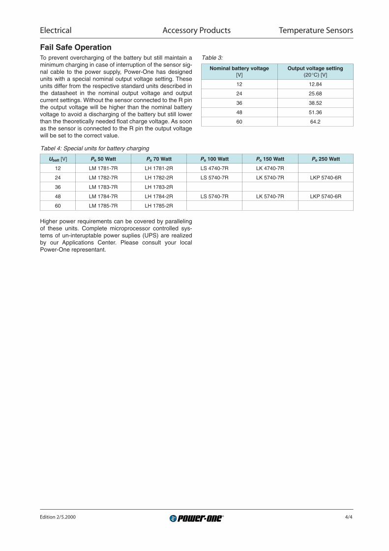
Fail Safe OperationTo prevent overcharging of the battery but still maintain aminimum charging in case of interruption of the sensor sig-nal cable to the power supply, Power-One has designedunits with a special nominal output voltage setting. Theseunits differ from the respective standard units described inthe datasheet in the nominal output voltage and outputcurrent settings. Without the sensor connected to the R pinthe output voltage will be higher than the nominal batteryvoltage to avoid a discharging of the battery but still lowerthan the theoretically needed float charge voltage. As soonas the sensor is connected to the R pin the output voltagewill be set to the correct value.
Table 3:
Nominal battery voltage Output voltage setting[V] (20°C) [V]
12 12.84
24 25.68
36 38.52
48 51.36
60 64.2
Higher power requirements can be covered by parallelingof these units. Complete microprocessor controlled sys-tems of un-interuptable power suplies (UPS) are realizedby our Applications Center. Please consult your localPower-One representant.

Electrical Accessory Products Filter & Ring Core Chokes
Edition 5/6.2000 1/5
Filters and Ring Core Chokes FP SeriesL Series
LP SeriesDescription
These Filters and chokes are designed to reduce input in-terference and/or output ripple voltages occurring in appli-cations with switched mode power supplies. Since all ourfilters contain a Moly Permalloy Powder (MPP) ring corethey feature very low DC losses as well as high DC mag-netisation and operate perfectly at the input and/or outputof switching regulators ensuring effective filtering even atelevated DC current levels. These special characteristicsallow the chokes to be operated at DC currents which con-siderably exceed the rated current, by accepting a corre-sponding gradual loss of inductance (unlike ferrite corechokes where inductance rapidly decreases above a cer-tain DC magnetising level).
In applications where switching regulators have long supplylines, filters and chokes are used in order to prevent oscilla-tions caused by their negative input impedance. For furtherinformation refer also to switching regulator data for "OptionL", and to section: Technical Information: Installation & Ap-plication.
Table 1a: Type survey of FP filter blocks
Filter type Part number Matching switchingregulator type
FP 38 HZZ 00903 PSR 54PSA 55PSA 5A2PSA 5A5PSA 123PSA 153
FP 80 HZZ 00904 PSR 53PSR 122.5PSR 152.5PSR 242PSR 362PSA 242.5
FP 144 HZZ 00905 PSA 121.5PSA 151.5PSA 241.5PSA 361PSA 481
Table 1b: Type survey ring core chokes
Type Inductivity ILn Single Symm. Partcoil coil number
LP 34-3 34 µH 3 A • HZZ 00501
L 20-7 20 µH 7 A • HZZ 00502
LP 20-7 20 µH 7 A • HZZ 00503
LP 183 2 × 183 µH 8 A • HZZ 00504
Filter Blocks FP TypesThe filter blocks contain, in addition to a MPP ring core, acapacitor and an attenuation resistor, capable of handlingthe high ripple currents seen at the input of switching regu-lators. This forms a complete external filter system opti-mised to prevent oscillations and to reduce superimposed
interference voltages and currents, specially designed foruse in PCB applications together with switching regulatorsin an A01 case size. For selection of filters refer to the typesurvey.
Table of Contents Page
Description ....................................................................... 1Filter Blocks FP Types ..................................................... 1
Page
Low-Loss Ring Core Chokes L/LP-Series ........................ 3Mechanical Dimensions ................................................... 5

Electrical Accessory Products Filter & Ring Core Chokes
Edition 5/6.2000 2/5
Electrical Data Filter Blocks
General Condition: TA = 25°C unless otherwise specified
Table 2: Filter blocks FP
Characteristics Conditions FP 38 FP 80 FP 144min typ max min typ max min typ max Unit
IFn Rated current L = 0.75 Lo 4 4 2 A DC
UFn Rated voltage TC min...TC max 5 40 5 80 15 144 V DC
RF Ohmic resistance 18 20 22 18 20 22 90 95 100 mΩ
Lo No load inductance IL = 0, TC min...TC max 30 34 38 30 34 38 88 100 112 µH
TA Ambient temperature IF = IFn –40 80 –40 80 –40 95 °C
TC Case temperature –40 92 –40 92 –40 98
TS Storage temperature –40 100 –40 100 –55 100
For currents IF > 4 A the following derating takes place: TA max = 100 – 1.3 • IF2 [°C], TC max = 100 – 0.49 • IF2 [°C]
Reduction of Output Ripple
Even though switching regulators have an inherently lowoutput ripple, certain sensitive applications need even fur-ther reduction. In such cases, the filters designed to reducedisturbances at the input, can also be used for reducing theripple on the output voltage (even better results with regardto the ripple and dynamic control deviation can be achievedby using low-loss ring core chokes in combination with anexternal capacitor, see below).
The output ripple can be reduced by the use of filter blocksby about 24 dB. The formula for the ripple uR at the load RL
is as follows:
uR = 0.063 • uo
(Ripple voltage uo is given for specific regulators in the cor-responding data section).
Consider, that the filter not only affects the output ripple butcan also influence the voltage across the load RL in theevent of load changes. The static load regulation increaseswith the ohmic resistance of the choke i.e. 24 mV/A for theFP 38 and FP 80 filters and 95 mV/A for the FP 144 filter.
Vi+
Gi–
Vo+
Go–
PSR RLURU
FilterUioUii
GiUo
12010
Fig. 2Reduction of voltage interference by FP filters
Input Interference Reduction
An AC ripple current can be measured at the input of anyswitching regulator, even if they are equipped with an inputfilter. Depending on the types of filters used, common and/or differential mode interferences can be reduced. They willalso help to further increase the surge and burst immunityof the power supplies.
The FP filters considerably increase the source impedanceof the regulators superimposed interference, to a valuewhich is normally high in comparison to the impedance ofthe source (ZLine). The interference currents are thereforepractically independent of their source impedance. The fil-ter will reduce these currents by approximately 25 dB at afrequency of 150 kHz.
The interference voltages at the filter input are due to theremaining interference currents flowing through the sourceimpedance. The resulting interference voltage reductioncan be seen in the following figure. For frequencies abovethe regulator switching frequency the attenuation will in-crease (up to 2 MHz approx.).
Parallel operation: When several switching regulator inputsare connected in parallel, each regulator should beequipped with a separate input filter. Interconnectionsshould only be made in front of the filter or at its input Uii(i. e. the central ground point should be before or at the filterand under no circumstances at the regulator input).
0 1 2 3 4 5 6
10
20
30
40
ZLine [Ω]
Source impedance
0Inte
rfer
ence
vol
tage
red
uctio
n
Att. [dB]inductiveresistivecapacitive 12009
Fig. 1Interference voltage reduction with FP filters at f = 150 kHz
Electrical Accessory Products Filter & Ring Core Chokes
Edition 5/6.2000 3/5
Typical Application
The example in figure Reduction of voltage interference byFP filters shows a switching regulator operating from a bat-tery (Ri < 0.5 Ω) with long supply lines (e.g. 2 m). The result-ing superimposed interference voltage USL may be meas-ured at the regulators input. The connection of a filter infront of the power supply will reduce this interference ac-cordingly:
1. The regulator's source impedance is mainly inductive be-cause of the low battery impedance and the long supplylines. It can be calculated as follows:
ZLine ≅ 2 π • fS • LLine • 2 l
ZLine ≅ 2 π • (150 • 103) • 10-6 • 2 • 2 ≅ 3.8 ΩfS: Switching frequency (150 kHz)
LLine : Supply line inductance (typically 1µH/m)
l : Length of single supply line (twice for posi-tive and negative path)
Fig. 3Reduction of voltage interference by FP filters
Vi+
Gi–
Vo+
Go–
PSR RLUoU
FilterUioUii
GiUs
2 • l
ZLine
12011
2. This example shows, that with an inductive source im-pedance of 3.8 Ω, the insertion of the filter results in aninterference voltage reduction of approx. 18 dB (seefig.: Interference voltage reduction with FP filters at f =150 kHz).
3. The original superimposed interference voltage will bereduced by a factor of approx. 8:
USF = USL • 10–18/20 [V]
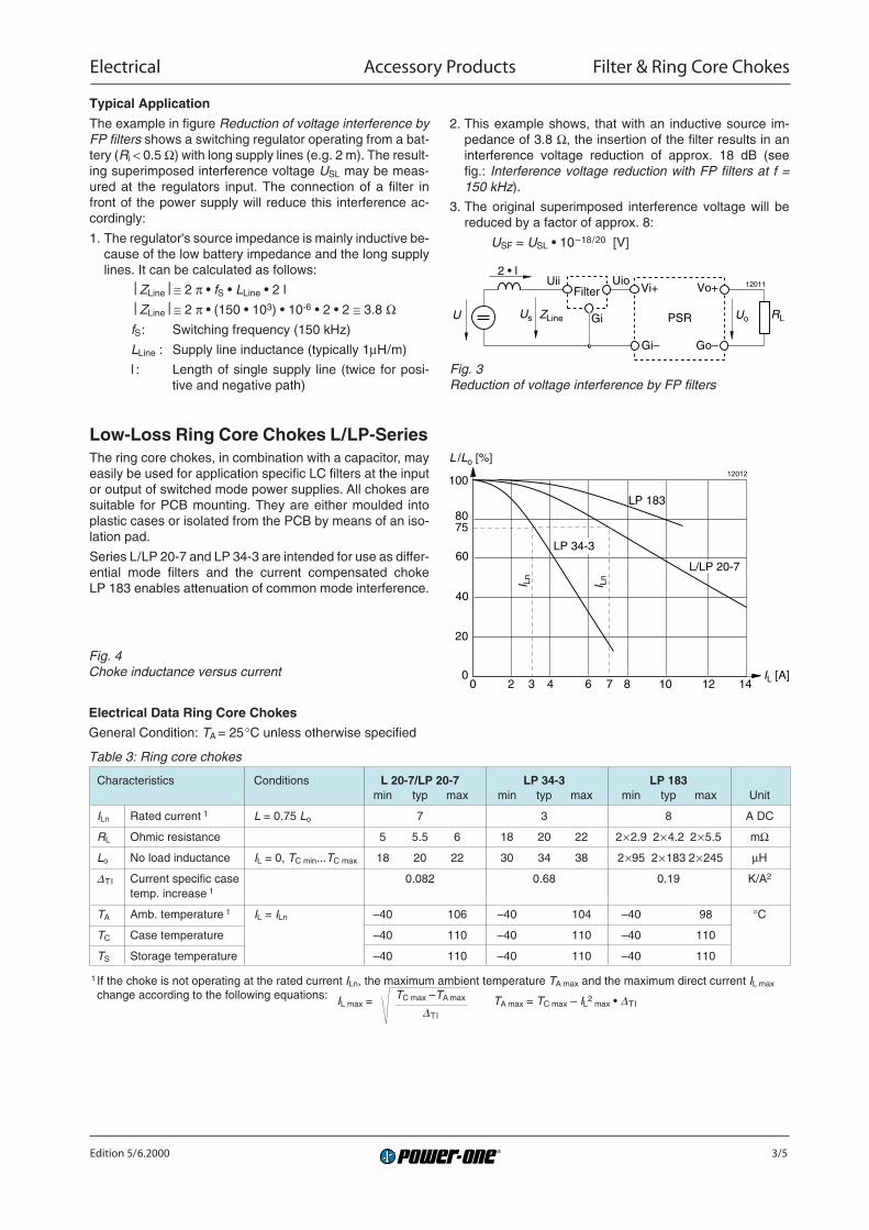
Electrical Data Ring Core Chokes
General Condition: TA = 25°C unless otherwise specified
Table 3: Ring core chokes
Characteristics Conditions L 20-7/LP 20-7 LP 34-3 LP 183min typ max min typ max min typ max Unit
ILn Rated current 1 L = 0.75 Lo 7 3 8 A DC
RL Ohmic resistance 5 5.5 6 18 20 22 2×2.9 2×4.2 2×5.5 mΩ
Lo No load inductance IL = 0, TC min...TC max 18 20 22 30 34 38 2×95 2×183 2×245 µH
DTI Current specific case 0.082 0.68 0.19 K/A2
temp. increase 1
TA Amb. temperature 1 IL = ILn –40 106 –40 104 –40 98 °C
TC Case temperature –40 110 –40 110 –40 110
TS Storage temperature –40 110 –40 110 –40 110
1 If the choke is not operating at the rated current ILn, the maximum ambient temperature TA max and the maximum direct current IL max
change according to the following equations: IL max =TC max –TA max TA max = TC max – IL2
max • DTIDTI
Low-Loss Ring Core Chokes L/LP-SeriesThe ring core chokes, in combination with a capacitor, mayeasily be used for application specific LC filters at the inputor output of switched mode power supplies. All chokes aresuitable for PCB mounting. They are either moulded intoplastic cases or isolated from the PCB by means of an iso-lation pad.
Series L/LP 20-7 and LP 34-3 are intended for use as differ-ential mode filters and the current compensated chokeLP 183 enables attenuation of common mode interference.
80
60
40
0
20
0 2 64 128 10 14
100
73
75
LP 34-3
LP 183
L/LP 20-7
12012
L /Lo [%]
I Ln
I Ln
IL [A]
Fig. 4Choke inductance versus current

Electrical Accessory Products Filter & Ring Core Chokes
Edition 5/6.2000 4/5
Input Interference Reduction
Using L- or LP-series chokes together with an additionalexternal capacitor a similar attenuation can be achieved aswith filter blocks. The capacitor between the choke and theconverter input is necessary in order to avoid possible oscil-lations caused by the negative input impedance of the regu-lator. This phenomenon could cause the input voltage toleave the specified regulator input range. The relativelyhigh ripple current flowing through the capacitor must beconsidered for the design. Refer also to: Technical Informa-tion: Installation & Application.
The current compensated choke LP 183 has a high perme-ability ring core with two identical separate windings. Thenormal operating current will only see the small stray in-ductance between the windings. However common modeinterference will be blocked by the full inductance of thechoke.
Fig. 7Low-loss ring core choke with external capacitor (Cex
approx. 1000 µF) used as output filter
Reduction of Output Ripple
Even though switching regulators have an inherently lowoutput ripple, certain sensitive applications need even fur-ther reduction. In such cases, the low-loss ring core chokesdesigned to reduce disturbances at the input can also beused for reducing the ripple on the output voltage. Thechokes in combination with an external capacitor canachieve even better results than the Filter Blocks with re-gard to the ripple and dynamic regulation.
The formula for the remaining output ripple at the load RL iscalculated as follows:
UR = uo • ZCex/ZLD
uo: Output ripple of the regulator
ZCex: The impedance of the capacitor at the regu-lator's switching frequency (150 kHz) corre-sponds to the equivalent series resistance(ESR) of the capacitor (please refer to thecorresponding data sheet).
ZLD = 2 π • fS • LD
fS: 150 kHz (regulator switching frequency)
Through the use of a common mode choke LP 183, thecommon mode noise at the output can also be further re-duced.
Consider that the filter not only affects the output ripple butcan also influence the voltage UR across the load RL in theevent of load changes. The static regulation increases withthe ohmic resistance of the choke, i.e. 6 mV/A for the chokeL/LP 20-7 and 20 mV/A for the LP 34-3.
The dynamic regulation is dependent on the size of the ca-pacitor. Generally, the bigger Cex the smaller is the dy-namic, however, recovery will be slower.
Typical Application
A voltage drop UrGo = rGo • (Io – Ii) is produced across theground loop resistance rGo. It is superimposed upon theregulators output voltage Uo and generates the voltage UR
= Uo – Ur Go across the load resistance RL. Without an inputinductance Le the current Ii in the input circuit has a rela-tively high AC component with a basic frequency fs (regula-tor's switching frequency of approx. 150 kHz). This alternat-ing current produces an AC voltage component across rGo
which is superimposed upon URL.
To prevent this phenomenon, an inductance Le can be in-serted into the input circuit. This causes the AC componentof the input current to be supplied entirely from the inputcapacitor Ce; thus, Ii is a pure direct current. Ce should bewired as close as possible to the regulator's input terminalsVi+ and Gi–.
Le and Ce additionally provide protection against input tran-sients and reduce radio interference voltages.
External connection of Gi– and Go– or connection via acommon ground is not recommended. The internal voltagedrop UrG in the regulator would be superimposed on theoutput voltage.
Vi+
Gi–
Vo+
Go–
PSRCe
UoU
12014
UR RL
RD LD ZLD ZC ext
Fig. 5L/LP type chokes and capacitors used as input filter
Vi+
Gi–
Vo+
Go–
PSRU
Cext 1 Cext 2 Cext 3
LP 34-3 orL/LP 20-7LP 183
12013
Uo RL
Vi+
Gi–
Vo+
Go–
PSRRLUoU Ce
Le
Ur G
rGo
rG
Ur Go
Io
URL
12015
Fig. 6Reduction of superimposed interference voltages ingrounded power supply systems, caused by ground loops

Electrical Accessory Products Filter & Ring Core Chokes
Edition 5/6.2000 5/5
Mechanical DimensionsDimensions in mm. Tolerances ±0.2 mm unless otherwise specified
Fig. 10Differential mode choke LP 34-3, weight 7 g
Fig. 9Differential mode choke L 20-7, weight 30 g
Fig. 11Common mode choke LP 183, weight 7 g
2738.147.5
13.7
22 ±1
3.6
30
7.5
±1
ø 3.8
4
6
0.8
1201
7
2 x 5.0817.5
10
15
±1ø 1
5.08
M 2.5
ø 0.8
1201
8
3 –0
.5 5.08
max
14.
5
7.6
13.2 7.5
max 8
ø 0.9
1201
9
37.8
±0.
5
ø1.
3 ±1
M 2
.5 0.9
x 0.
56
25 ±0.5
min. 4.5
1 3.22 ±0.5 (3.22)b
3.66
10.1
615
.24
(3.6
6)16.6 ±1
4
12
3
4
6.8 ±1
b
b
Legend: b = 5.08 mm1 = Uii (input)2 = Uio (output)3 = Gi (ground)4 = Positioning pins
1201
6
Fig. 8Filter blocks FP weight 30 g
EuropeanProjection

Electrical Accessory Products Back Planes
Edition 5/6.2000 1/14
Back Planes for the T Series BPD SeriesBPF Series
19"/3U Rack-Systems
• Easy configuration of telecom rectifiers, batterychargers and power bus systems
• Provides controller function
• 1.6 kW maximum power
• Single or triple phase connection
• Redundant configuration possible
Table of Contents Page
Summary .......................................................................... 1Type Survey and Key Data .............................................. 2Functional Description...................................................... 2Mains Input Section.......................................................... 4Output Section ................................................................. 5
SummaryThe back plane types BPF 1000 and BPD 1000 have beendesigned for fast and simple set-up of 19" rack mountedpower supply systems powered by AC-DC converters ofthe T series. Battery charger systems, telecom rectifiersand modular power bus systems can easily be configuredwith n+1 redundancy if required. Three T units can beplugged into one back plane providing up to 1.6 kW outputpower.
Since for such applications the status of the power bus is ofimportance rather than the output status of a single AC-DCconverter, T units with option D should be choosen enablingremote bus voltage sensing.
The back plane concept allows system assembly in next tono time. When fitted in the rack all input and output termi-nals are readily accessible from the rear. The AC input isdesigned for single or 3-phase operation. The monitoringsignals and the control signal inputs and outputs are avail-able from a screw terminal strip. System specific signalcombination is possible with different jumper settings. Theback plane fulfills in this way the function of a controller unit.
The layout of the back plane and the hot plug-in capabilityof the AC-DC converters allow system expansion underload (e.g. from 550 W up to 1.6 kW) by simply inserting fur-ther T units into the rack. Larger system power extension isjust a matter of interlinking the DC output rails and signaloutputs of two or more racks.
The back planes are available in 2 basic versions:
– BPD 1000A front-end version, fitted with decoupling diodes in eachpositive line to the DC bus, for systems with 2 or moreT units in parallel or n+1 redundancy.
– BPF 1000A battery charger version, in which each output is fittedwith a fuse in the positive line to the DC bus, for batterycharging or rectifier systems with two or more T units inparallel or n+1 redundancy.
For minimum electromagnetic emission at the input, boththe BPD and the BPF versions are fitted with input filters.Should project specific requirements demand enhancedhold-up time or lower output ripple (low frequency ripple)than specified for the individual AC-DC converters, bothbasic back plane versions are available with additional out-put capacitors.
Important: The neccessity to provide a cover over thelive parts at the mains input (High Voltage) or over theDC bus bars (Energy Danger), preventing accidentalcontact during installation, start-up of a system or main-tenance, depends on the final installation as well as onthe applicable safety requirements. However, it is the re-sponsibility of the installer or user to provide such asafety cover to assure the compliance with the relevantand applicable safety standards.
Page
Electromagnetic Compatibility (EMC) .............................. 7System Integration ........................................................... 8Mechanical Data ............................................................ 10Safety and Installation Instructions ................................ 10

Electrical Accessory Products Back Planes
Edition 5/6.2000 2/14
Type Survey and Key DataTable 1: Type survey
AC Input Input filters 1 Output capacitors Preload Application85...255 V AC (reduced 100 Hz
1 or 3 phase (Y) output ripple) 2
BPD 1002 x – – Front-end, fitted with diodesBPD 1003 x 90 mF –
BPF 1004 x – x Battery charger, fitted with fusesBPF 1007 x 50 mF xBPF 1006 x 90 mF x
BPF 1037 (∆) 3 x 50 mF x BPF 1007 in ∆ configuration
19” Rack, 3 U Rack for systems with up to 3 T units
1 See also: Electromagnetic Compatibility.2 Please refer to: Dimensioning Example of a Battery Charger System in Single Phase Connection3 Only for LT units and 120/208 V mains. See fig.: Mains input arrangement.
Functional DescriptionThe back plane is divided into 3 sections, each one fittedwith an H15 female connector for one T unit, with the mainsinput section and the DC output section separated fromeach other.
The layout of the standard back planes gives the user theflexibility to operate the system either in single phase orin 3-phase (Y) configuration. Connection to the mains isachieved via the 6-pole connector (X1). With the wire jump-ers B10/20/30 in Y-position (standard configuration) eachT unit is connected between its defined input line and theneutral. (Changing of the configuration by the customer isnot recommended.) An input filter, provided in the supplyline to each T unit minimizes the conducted noise at the in-put of the system. The positive output of each T unit isseparately fed to the common power bus and is decoupleddepending upon the back plane type, either by a fuse (F11/21/31) or by a decoupling diode (D11/21/31). The fuses(cartridge type) are externally accessible from the frontside.The BPF versions are fitted with a common preload (R25).Additional output capacitors (up to 3 per output,10 mF
each) further reduce the low frequency output ripple andprovide enhanced hold-up time.
All relevant monitoring signals as well as control signal in-puts and outputs are accessible at the signal terminal strip(X5). The jumper strip (X3) allows system specific signalsaccording to different jumper settings. An auxilliary cir-cuit (protected by a fuse F1, rated T1A, 250 V, 5 × 20 mm)allows a relay to be directly driven for system specific con-trol functions.
Each T unit provides an individually adjustable power downsignal enabling bus status monitoring at different voltagelevels. The threshold values can be set at the soldering tabsDset (R13/14, R23/24 and R33/34).
Note: If a power system is operated with 3 T units per back-plane, connection to the mains in a 3-phase configuration(Y or ∆) will provide equal load distribution on the inputlines. Furthermore the low frequency ripple at the output ofthe T units is compensated to zero as long as all 3 T unitsare in operation.

Electrical Accessory Products Back Planes
Edition 5/6.2000 3/14
Input filter Input filter Input filter123
Fuse F1(auxiliary circuit)
Bus bar system Output capacitor (10 mF, each)
Dset T1
Preload (<10 W)
Signal terminal strip X5
Jumper strip X3
Mains input connector X1Connector H15 for T unit
+
–
Output fuse
Y
Y
L1L2L3N
X4
B30Y
B20
B10
0301
2
R33 R34
F31
R23 R24R25
F21
R13 R14
F11
D31 D21 D11
Decouplingdiode
Fig. 1Back plane, view from the rear
F
F
F
+ + +
+ + +
+ + +
X1
L1
L2
L3
N
Vo+
Vo–
D set
Sys In
Di
Sys out
D2
D1
D3
F11
F31
C C C
C C C
C C C
D31
D21
D11
RPT
RPT
RPT
+
+
–
–
Vo+
Vo–
P
N
Y
Y
Y
Vo+ (BUS)
Vo+ (BUS)
Vo+ (BUS)
Sys In 2
Sys In 3
Sys In 1
F21Vo+
Vo–
D set
Sys In
Di
Sys out
P
N
Vo+
Vo–
D set
Sys In
Di
Sys out
P
N
R13
R23
R33
R14
R24
R34
0301
3
DC-Bus
B10
B20
B30
T unit 1
T unit 2
T unit 3
R25
Fig. 2Block diagram of back planeF11, 21, 31 fitted to BPF types. D11, 21, 31 fitted to BPD types.

Electrical Accessory Products Back Planes
Edition 5/6.2000 4/14
Phase to Phase ConfigurationWith standard back plane version (Y-configuration)
For LT units exclusively
The layout of the standard back planes also allows phase tophase connection at low mains voltage 208 V e.g. USA, pro-viding full output power from the LT units. In such cases oneof the two input lines (L1 or L2) should be connected to theN-terminal at the AC input connector instead of the neutralline. The neutral line is not connected. For safety reasonsan external fuse should be fitted in each input line. Connec-tion to the ground is mandatory.
Fig. 5Phase to phase configuration L1, L2120/208 V mains (e.g. USA): LT types only.Not applicable for UT types.
Control circuit
Go–
Vo+
Gi–
Vi+
Inp
ut
Filte
r
R
Io
Uo
Ii
U i
03019
Ce
29
26
20
23
32
14
17
2
8
11
Mains Input Section
Connection to the Mains
Connection to the mains shall be made via the 6-pole screwterminal connector (X1), located on the right hand side ofthe back plane (view from the rear).
For single phase operation the terminals (L1, L2 and L3) atthe female connector X1 should be connected together.The T-series has two AC input voltage ranges. The LT unitsare optimized for the 230 V mains, the UT units for the120 V mains. (See also: T series)
Table 2: Mains input arrangement
Mains voltage Single phase 3-phase (Y) Phase - phase (∆) 3-phase (∆)Phase-Earth/Phase-Phase L, N, L1, L2, L3, N, L1, L2, L1, L2, L3,
230/400 V LT types LT types Not allowed Not allowed
120/208 V LT types LT types only With special back planeUT types External fuses required BPF 1037 and
LT types only
Single-phase/3-phase (Y) ConfigurationStandard back plane version (Y-configuration)
The layout of the standard back planes allows operation ofthe system either in single phase or in 3-phase (Y) configu-ration. In both configurations each T unit on the back planeis connected between its defined phase and neutral. Forsingle phase operation the AC-input terminals (L1, L2 andL3) should be connected together at the female connector.Connections to neutral and to ground are mandatory. (Seealso fig.: Single phase configuration as well as fig.: 3-phase(Y) configuration.) Equal load distribution on the input linesat 3-phase configuration will compensate the low frequencyripple at the output to zero.
Control circuit
Vo–
Go+
Vi–
Gi+
Input F
ilte
r
R (option)
i (option)
Io
–Uo
Ii
–U i
03017
Ce
Option P
Control circuit
Option P
Go–
Vo+
Gi–
Vi+
Inp
ut
Filte
rO
ptio
n L
G
R
i
D (option)
Io
Uo
I i
U iOption C
Option C
03018
Option D
Fig. 3Single phase configuration L, N230 V mains: LT-types
Fig. 43-phase (Y) configuration L1, L2, L3, N230/400V mains: LT-types120/208V mains: UT-types, LT-types 1
1 Reduced output power with LT types
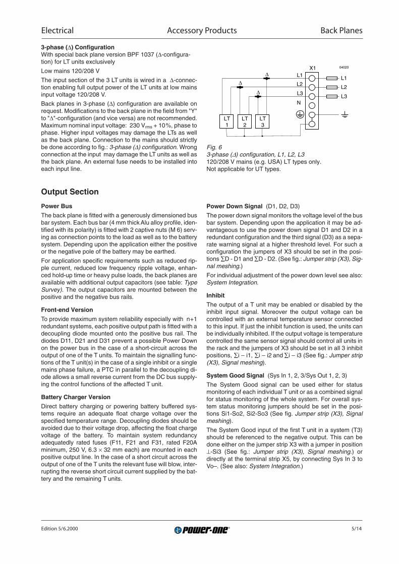
Electrical Accessory Products Back Planes
Edition 5/6.2000 5/14
3-phase (∆) ConfigurationWith special back plane version BPF 1037 (∆-configura-tion) for LT units exclusively
Low mains 120/208 V
The input section of the 3 LT units is wired in a ∆-connec-tion enabling full output power of the LT units at low mainsinput voltage 120/208 V.
Back planes in 3-phase (∆) configuration are available onrequest. Modifications to the back plane in the field from "Y"to "∆"-configuration (and vice versa) are not recommended.Maximum nominal input voltage: 230 Vrms + 10%, phase tophase. Higher input voltages may damage the LTs as wellas the back plane. Connection to the mains should strictlybe done according to fig.: 3-phase (D) configuration. Wrongconnection at the input may damage the LT units as well asthe back plane. An external fuse needs to be installed intoeach input line.
Fig. 63-phase (D) configuration, L1, L2, L3120/208 V mains (e.g. USA) LT types only.Not applicable for UT types.
L1
LT3
X1L1
L2
L3
N
LT2
LT1
L2
L3
04020
∆∆
∆
Output Section
Power Bus
The back plane is fitted with a generously dimensioned busbar system. Each bus bar (4 mm thick Alu alloy profile, iden-tified with its polarity) is fitted with 2 captive nuts (M 6) serv-ing as connection points to the load as well as to the batterysystem. Depending upon the application either the positiveor the negative pole of the battery may be earthed.
For application specific requirements such as reduced rip-ple current, reduced low frequency ripple voltage, enhan-ced hold-up time or heavy pulse loads, the back planes areavailable with additional output capacitors (see table: TypeSurvey). The output capacitors are mounted between thepositive and the negative bus rails.
Front-end Version
To provide maximum system reliability especially with n+1redundant systems, each positive output path is fitted with adecoupling diode mounted onto the positive bus rail. Thediodes D11, D21 and D31 prevent a possible Power Downon the power bus in the case of a short-circuit across theoutput of one of the T units. To maintain the signalling func-tions of the T unit(s) in the case of a single inhibit or a singlemains phase failure, a PTC in parallel to the decoupling di-ode allows a small reverse current from the DC bus supply-ing the control functions of the affected T unit.
Battery Charger Version
Direct battery charging or powering battery buffered sys-tems require an adequate float charge voltage over thespecified temperature range. Decoupling diodes should beavoided due to their voltage drop, affecting the float chargevoltage of the battery. To maintain system redundancyadequatedly rated fuses (F11, F21 and F31, rated F20Aminimum, 250 V, 6.3 × 32 mm each) are mounted in eachpositive output line. In the case of a short circuit across theoutput of one of the T units the relevant fuse will blow, inter-rupting the reverse short circuit current supplied by the bat-tery and the remaining T units.
Power Down Signal (D1, D2, D3)
The power down signal monitors the voltage level of the busbar system. Depending upon the application it may be ad-vantageous to use the power down signal D1 and D2 in aredundant configuration and the third signal (D3) as a sepa-rate warning signal at a higher threshold level. For such aconfiguration the jumpers of X3 should be set in the posi-tions ∑D - D1 and ∑D - D2. (See fig.: Jumper strip (X3), Sig-nal meshing.)
For individual adjustment of the power down level see also:System Integration.
Inhibit
The output of a T unit may be enabled or disabled by theinhibit input signal. Moreover the output voltage can becontrolled with an external temperature sensor connectedto this input. If just the inhibit function is used, the units canbe individually inhibited. If the output voltage is temperaturecontrolled the same sensor signal should control all units inthe rack and the jumpers of X3 should be set in all 3 inhibitpositions, ∑i – i1, ∑i – i2 and ∑i – i3 (See fig.: Jumper strip(X3), Signal meshing).
System Good Signal (Sys In 1, 2, 3/Sys Out 1, 2, 3)
The System Good signal can be used either for statusmonitoring of each individual T unit or as a combined signalfor status monitoring of the whole system. For overall sys-tem status monitoring jumpers should be set in the posi-tions Si1-So2, Si2-So3 (See fig. Jumper strip (X3), Signalmeshing).
The System Good input of the first T unit in a system (T3)should be referenced to the negative output. This can bedone either on the jumper strip X3 with a jumper in position⊥-Si3 (See fig.: Jumper strip (X3), Signal meshing.) ordirectly at the terminal strip X5, by connecting Sys In 3 toVo–. (See also: System Integration.)

Electrical Accessory Products Back Planes
Edition 5/6.2000 6/14
X3
X5F 1T1A, 250 V
Vo+
Vo–
1
2
3
4
5
6
7
8
9
10
11
12
13
14
15
16
17
18
19
20
21
22
23
24
∑D - D1
∑D - D2
∑D - D3
∑D - Si3
∑i - i1
∑i - i2
∑i - i3
Si1 - So2
Si2 - So3
- Si1
- Si2
- Si3
14
13
12
11
10
9
8
7
6
5
4
3
2
1
Vo+
D1
D2
D3
i1/Ucr
i2/Ucr
i3/Ucr
Sys Out 1
Sys Out 2
Sys Out 3
Sys In 1
Sys In 2
Sys In 3
Vo–
D1
D2
D3
i1/U
cr
i2/U
cr
i3/U
cr
Sys
Out
1
Sys
Out
2
Sys
Out
3
Sys
In 1
Sys
In 2
Sys
In 3
05029
Vo–
Fig. 7Jumper strip (X3), signal meshing
Table 3: Terminal strip X5
Connector X5 Signal allocation Description
1 Vo– Supply Vo-
2 Sys In 3 Sys Good input T3
3 Sys In 2 Sys Good input T2
4 Sys In 1 Sys Good input T1
5 Sys Out 3 Sys Good output T3
6 Sys Out 2 Sys Good output T2
7 Sys Out 1 Sys Good output T1
8 i3/Ucr Inhibit T3/Ucr
9 i2/Ucr Inhibit T2/Ucr
10 i1/Ucr Inhibit T1/Ucr
11 D3 Power Down T3
12 D2 Power Down T2
13 D1 Power Down T1
14 Vo+ Supply Vo+
Interface for Remote Signalling and Control
A signal terminal strip (X5) allows interfacing with the cus-tomer‘s control system.
Each of the signals can be made available as an individualsignal or as a combined signal.
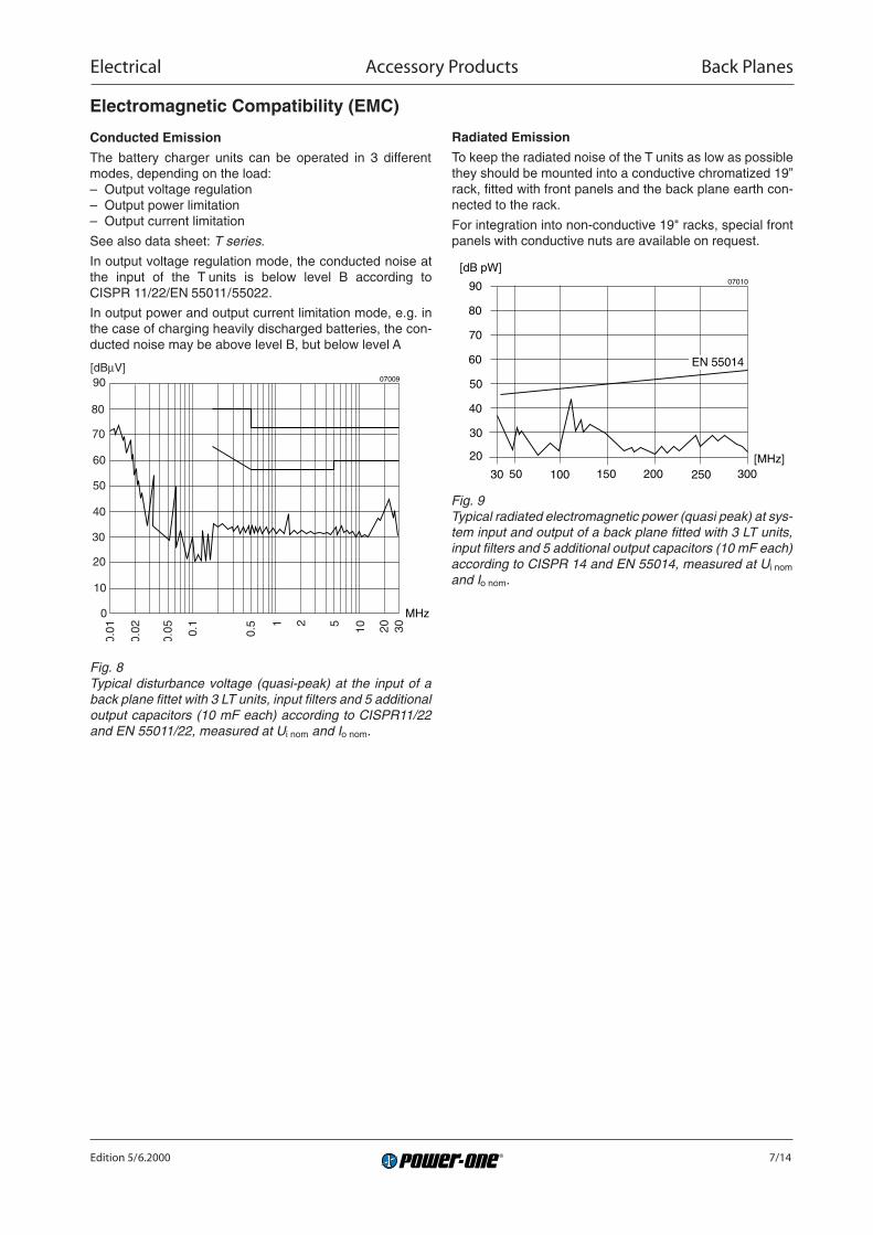
Electrical Accessory Products Back Planes
Edition 5/6.2000 7/14
Electromagnetic Compatibility (EMC)
Conducted Emission
The battery charger units can be operated in 3 differentmodes, depending on the load:– Output voltage regulation– Output power limitation– Output current limitation
See also data sheet: T series.
In output voltage regulation mode, the conducted noise atthe input of the T units is below level B according toCISPR 11/22/EN 55011/55022.
In output power and output current limitation mode, e.g. inthe case of charging heavily discharged batteries, the con-ducted noise may be above level B, but below level A
Radiated Emission
To keep the radiated noise of the T units as low as possiblethey should be mounted into a conductive chromatized 19”rack, fitted with front panels and the back plane earth con-nected to the rack.
For integration into non-conductive 19" racks, special frontpanels with conductive nuts are available on request.
90
80
70
60
50
40
30
20
10
0
0.01
0.05 0.
1
0.5 1 2 5 10 20 30
[dBµV]
MHz
0.02
07009
20
30
40
50
60
70
80
90
[dB pW]
[MHz]50 100 150 200 250 30030
EN 55014
07010
Fig. 8Typical disturbance voltage (quasi-peak) at the input of aback plane fittet with 3 LT units, input filters and 5 additionaloutput capacitors (10 mF each) according to CISPR11/22and EN 55011/22, measured at Ui nom and Io nom.
Fig. 9Typical radiated electromagnetic power (quasi peak) at sys-tem input and output of a back plane fitted with 3 LT units,input filters and 5 additional output capacitors (10 mF each)according to CISPR 14 and EN 55014, measured at Ui nom
and Io nom.

Electrical Accessory Products Back Planes
Edition 5/6.2000 8/14
Battery Selection
When selecting a battery, the following aspects should beconsidered:
1. Batteries are normally specified at 20°C.Steady operation at higher temperatures will shorten thelife time of a battery. For every 10 K temperature in-crease the battery lifetime is halved.
2. Worst case considerations with regard to the necessarybattery capacity should include operation at the lowestpossible temperature and highest possible dischargecurrent, since under such conditions a substantial capac-ity drop has to be expected.
3. The capacity of a battery deteriorates with time. There-fore decisions on battery capacity should be based upon20% ageing loss.
4. Consult the battery manufacturer for correct layout of thebattery system.
Selecting the Right Battery and Back Plane Configura-tion
As mentioned in the T series data sheet the power factorcorrection at the input of the T unit generates a ripple volt-age at the output of twice the input frequency, causing a rip-ple current into the connected battery.
For most battery types the low frequency ripple currentshould not exceed 5 Arms per 100 Ah (0.05 C). Some manu-facturers (with newer battery technology) specify 10 Arms
per 100 Ah (0.1 C).
Excessive ripple current can increase the battery tempera-ture and reduces the battery lifetime. For a single phasesystem additional output capacitors may be necessary de-pending upon the selected battery type.
Note: With the T units symmetrically connected to a3-phase (Y) mains supply the low frequency output ripple isvirtually zero, only a high frequency ripple and noise of<100 mVpp at the switching frequency of 65.5 kHz remains.
System Integration
Mains Input Voltage Monitoring
The T unit interprets a mains failure as a system error, indi-cated by the red Error LED together with a System Goodfailure signal. Should a dedicated mains failure identifica-tion be required this signal would have to be established ex-ternally.
Available signals/signal combinations (Please also refer tothe: T series data sheet):
The T unit provides two open collector signals, SystemGood and Power Down.
The System Good signal monitors the operational functionof a single T unit. In case of reduced available output powerdue to a mains failure, a T unit failure or inhibit, the signalchanges from low to high impedance.
In systems with battery back-up or with n+1 redundancy thefailure of one single unit does not cause a failure of the sys-tem as the required output power is still available eitherfrom the battery or from the remaining T units. To indicatethe status of the whole system, the System Good signals ofall 3 units should be connected in series on the back plane.
The System Good output can be combined with similar out-puts of other DC-DC converters such as CQ units, integrat-ing the additional information into the overall system statussignal.
If only the system status of the T unit is to be monitored,Sys In should be wired to Vo–.
The Power Down signal monitors the output voltage level ofthe bus bar system. The threshold levels of the 3 possiblesignals can be individually adjusted by means of resistorsR 13/14...R 33/34 (see: T series data sheet) and be usedfor:• Save data• Disconnecting the load or part of it• Performing a battery test
In systems with battery back-up it may be desirable to ex-tend system operation in case of long term mains failuresby disconnecting an uncritical part of the load at a certainbus voltage level, triggered by one of the 3 possible powerdown signals. The 2 remaining signals can be set to the lowbattery discharge level to get a redundant signal (wiredAND) for finally disconnecting the critical part of the load.
Note: The Power Down signal has an enlarged hysteresisof approximately 6 V for T 1740 units and 3.5 V for T 1240units.
The Power Down signal(s) can be combined with the Sys-tem Good signal to give a wired AND (see: T series datasheet). In such cases the resulting alarm only becomes ac-tive as a result of a mains failure or a converter failure to-gether with a heavily discharged battery.

Electrical Accessory Products Back Planes
Edition 5/6.2000 9/14
Dimensioning Example of a Battery Charger Systemin Single Phase Connection
Battery charger system in single phase connection:230 V, 50 Hz, load: 1 kW, battery back-up: 3 h
Battery charger:3 LT 1740 , n+1 redundant configuration, 1.6 kW
Conditions:TA = –10...40°C for both, charger and battery
12
56
0300
0.6
0.2
0.4
1.0 10010
factor y(Irms bat /Iload)
Rsys [mΩ]
34
Number of LT units:
06037
Rback plane 1 Rtot supply lines
16 mΩ
–
Ri AC batLT 1
LT 2
LT 3
–
≈ 1.5 m
+
+
06039
1 The resistance on the back plane (Rback plane) is already takeninto account in the following two graphs.
Fig. 10System set-up
Battery specification (at 20°C):• 24 cells, 2.23 V/cell, float charge voltage 53.5 V• Permissible ripple current Irms bat: 0.05 C (5% of battery
capacity)• Temperature coefficient –3 mV/K per cell• Max. discharge current 20 A• Capacity at –10°C and 0.2 C discharge: 70%
Calculation of battery size:Load 20 A, back-up 3 h, ageing loss 20% therefore ageingfactor 0.8, derating factor for temperature and dischargecurrent 0.7
Qbat [Ah] = Iload • tback-up / (fageing • fTAIdischarge)= 20 [A] • 3 [h] /(0.8 • 0.7) = 107 [Ah]next closest battery configuration:: 120 Ah or 95 Ah
Decision: Battery with 95 Ah (Ri DC: 28 mΩ)
Calculation of the ripple current:The ripple current to the battery can either be measured orcalculated. The diagrams allow a good estimation of the re-lationship between the ripple current to the battery Irms bat
and the load current I Load of a given system resistance RSys.The system resistance is the sum of the resistance of thesupply and the AC resistance of the battery.The AC resistance is defined as the relationship betweenthe AC voltage and the AC current to the battery measuredwith a capacitively coupled 100 Hz AC source.In the example the system resistance is:RSys = Rsupply rms + Ri AC bat
= 16 mΩ + 16 mΩ = 32 mΩPermissible ripple current:Irms bat = 0.05 • 95 Ah = 4.75 Arms
Calculated ripple current:With 3 LT 1740 without capacitance on the back planeIrms bat = Iload • factor y = 19 A • 0.198 = 3.76 Arms = 0.04 C
With 3 LT 1740 and 50 mF on the back planeIrms bat = 19 A • 0.16 = 3.04 Arms = 0.032 C
With 3 LT 1740 and 90 mF on the back planeIrms bat = 19 A • 0.13 = 2.47 Arms = 0.026 C
All three examples give a value below the permissible ripplecurrent.
Fig. 11Irms bat/Iload versus system resistance (Rsys). Up to 6 T unitsin parallel, without additional output capacitors
Fig. 12Irms bat/Iload versus system resistance (Rsys). 2 and 3 T unitsin parallel, with additional output capacitors
2 units + 50 mF2 units + 90 mF
3 units + 50 mF3 units + 90 mF
0300
0.6
0.2
0.4
1.0 10010Rsys [mΩ] 32
0.16
factor y(Irms bat /Iload)
Number of LT units plus additional output capacitance
06038
Additional capacitance on the back plane not only reducesthe AC ripple on the battery, but stabilizes the output volt-age during fast load changes.
Where the ripple current should be reduced even more, thesystem resistance RSys could be increased with a specialchoke set into the battery supply line. For further informa-tion please contact Power-One.

Electrical Accessory Products Back Planes
Edition 5/6.2000 10/14
Table 5: Pin allocation of the signal terminal strip X5
Pin no. Electrical determination Pin designation
1 Supply negative (return potential) Vo–
2 Sys good input of T unit no. 3 Sys In 3
3 Sys good input of T unit no. 2 Sys In 2
4 Sys good input of T unit no. 1 Sys In 1
5 Sys good output of T unit no. 3 Sys Out 3
6 Sys good output of T unit no. 2 Sys Out 2
7 Sys good output of T unit no. 1 Sys Out 1
8 Inhibit or Ucr of T unit no. 3 i3/Ucr
9 Inhibit or Ucr of T unit no. 2 i2/Ucr
10 Inhibit or Ucr of T unit no. 1 i3/Ucr
11 Power down of T unit no. 3 D3
12 Power down of T unit no. 2 D2
13 Power down of T unit no. 1 D1
14 Supply positive Vo+
The signal terminal strip X5 is provided with a matching fe-male connector at delivery.
The jumper strip X3 is provided with 7 jumpers at delivery.
The pin allocation of the jumper strip is described in fig.Jumper strip (X3), signal meshing.
Safety and Installation Instructions
Transportation
For transportation use standard Power-One packaging ma-terial.
Racks fitted with back planes are not designed for transpor-tation with the T series AC-DC converters fitted into theracks.
Connector Pin Allocation
The power output is provided via the two bus bars, the posi-tive one designated Vo+, the negative one Vo–. The follow-ing pin allocation tables define the electrical potentials andthe physical pin positions on the connectors of the backplanes.
Table 4: Pin allocation of the mains input connector X1
Pin no. Electrical determination Pin designation
1 Input phase 1 L1
2 Input phase 2 L2
3 Input phase 3 L3
4 Input neutral N
5 Protective earth
6 Protective earth
Input connector X1 is provided with a matching male con-nector at delivery. Standard configuration: Pins 1, 2 and 3are interconnected (for single phase operation).
Mechanical DataDimensions in mm. Tolerances ±0.3 mm unless otherwise indicated. European
Projection
60
426.72
101.6 101.6 101.6 101.687.62
129.
54
3.5
09108
35.56 142.24 142.24
Safety cover
Fig. 13Back plane for 19" rack, weight: 1.7 kg

Electrical Accessory Products Back Planes
Edition 5/6.2000 11/14
Installation Instruction
The BPD/BPF series back planes are components, in-tended exclusively for inclusion within other equipment byan industrial assembly operation or by professional install-ers. Installation must strictly follow the national safety regu-lations in compliance with the enclosure, mounting, creep-age, clearance, casualty, markings and segregation re-quirements of the end-use application. See also: TechnicalInformation: Installation and Application.
Caution: It is the responsibility of the design engineerand of the installer to define and apply a safety conceptfor the whole system which is provided with a Power-One back plane. The following are under the aspectswhich have to be considered:
• Consult the T-series AC-DC converters data sheet priorto connecting the system to the mains.
• The necessity to provide a cover over the live parts at themains input (hazardous voltage) or over the DC-bus bars(energy hazard), preventing accidental contact during in-stallation, start-up of a system or maintenance, dependson the final installation as well as on the applicable safetyrequirements.
• Service should be carried out by qualified personnel only.• Fuses should be replaced with the same types only.• The earth terminal on the back plane must be connected
to safety ground.• Back planes in 3-phase (∆) configuration are available on
request. Modifications to the back plane in the field from"Y"- to "∆"-configuration (and vice versa) are not recom-mended.
• The maximum nominal input voltage is 230 Vrms +10%.Higher input voltages may damage the Tseries AC-DCconverters as well as the back plane.
• Empty spaces in a rack should be covered by a dummyfront panel.
Caution: Prior to handling, the back plane must be dis-connected from mains and from other sources (e.g. bat-teries). Check for hazardous voltages and hazardousenergy before and after altering any connections. Haz-ardous energy levels may be present at the output termi-nals even after the mains input voltage has been discon-nected from the unit. This is indicated by the red errorLEDs of the Tseries AC-DC converters. It is the respon-sibility of the installer to prevent an unwanted short-cir-cuit across the output of the back plane, of the batteryand of each T series AC-DC converter. In case of a shortcircuit across the output of a T unit, all LEDs will be off,although the mains may be present.
The back planes are intended for stationary applications.They shall be installed in 19’’ racks according to DIN 41494.
Install the back planes vertically, the mains input connectorX1 being on the right hand side of the back plane (view fromthe back) and make sure that there is sufficient air flowavailable for convection cooling of the T-series AC-DC con-verters.
Mechanical fixing shall be made via 10 screws M2.5 × 10and 10 nuts M2.5. When mounting a back plane to a rack,fit two T units into the H 15 female connectors on the backplane prior to fixing the back plane to the rack. This ensurescorrect positioning of the female connectors on the backplane with respect to the given position of the male connec-
tors of the T units in the rack. With the back plane improp-erly positioned, the connectors of the T units and the femaleconnectors on the back plane may be damaged. In order tomaintain correct positioning, use all the available mountingholes.
Connection to the supply system shall be made via the 6-pole screw terminal connector X1 according to: ConnectorPin Allocation and Mechanical Data.
The connector X1 of the back planes (class I equipment) isprovided with two protective earth terminals ( ), which arereliably connected with the protective earth pins of the con-nectors for the T units. For safety reasons it is essential toconnect at minimum one of these terminals with the protec-tive earth of the supply system. Since the earth leakagecurrent exceeds 3.5 mA, the system must be permanentlyconnected or it must be pluggable equipment type B ac-cording to IEC/EN 60950. The earth connection must beperformed before connecting the supply.
To maintain good electrical connection, the AC input, earthand signal to the terminal strip wiring should be secured,using tie wraps, to prevent stress upon the wires and theconnectors.
Refer to Mains Input Section to ensure that phase and neu-tral configuration matches with the back plane and TseriesAC-DC converter types. Wrong connection at the input maydamage the Tseries AC-DC converters as well as the backplane. Standard back planes are designed for a 3-phasesystem in Y connection with a phase to neutral voltage of230 V or 120 V where connection to neutral is mandatory.Integration into a 3-phase system in ∆ configuration (120/208 V and without connection to neutral) is only possiblewith LT AC-DC converters together with the special backplane BPF 1037.
For safety reasons, a mains switch for line interruption isrequired.
The back plane does not provide any input fuses. The inputfuses of the Tseries AC-DC converters in the connectionfrom the L terminal are designed to protect the units in caseof overcurrent and may not be able to satisfy all customerrequirements. An external input fuse suitable for the appli-cation and in compliance with the local requirements in thewiring to each phase and to the neutral terminal may there-fore be necessary to ensure compliance with local require-ments. A second fuse in the wiring to each input terminal isneeded if:• Standard back planes are used in phase to phase con-
figuration• Local requirements demand an individual fuse in each
source line• Neutral to earth impedance is high or undefined• Phase and neutral of the mains are not defined or cannot
be assigned to the corresponding terminals (L to phaseand N to neutral).
Important: Do not open the modules, or guarantee willbe invalidated.

Electrical Accessory Products Back Planes
Edition 5/6.2000 12/14
Additional Information for Installation of BatteryCharger Systems:
Reverse polarity connection of the battery may damage thebattery, the back plane(s) and the battery chargers.
Prior to putting a system into operation, check whether theposition of the cell voltage selector switch of each TseriesAC-DC converter corresponds to the required battery cellvoltage.
For battery maintenance please contact the battery manu-facturer.
Exchanging a battery should always include the whole bat-tery bank. New batteries should be of the same type, withthe same cell voltage and temperature coefficient.
For expansion of battery systems contact the battery manu-facturer.
For battery location and connection please refer to VDE0510, part 2.
In battery charger systems, safety standards demand that abattery can be completely disconnected from the powersystem including the battery system ground. Dependingupon the project specific requirements, disconnecting mayeither occur by a manually operated switch with fuses, orautomatically by means of a circuit breaker.
Caution: Care should be taken during system set-up orafter maintenance when connecting a battery to thepower bus of a back plane (BPF types) fitted with fuses.The T series AC-DC converter system with the backplanes should be switched to the mains prior to connect-ing the battery to the power bus, since the reverse cur-rent from the battery into the uncharged output capaci-tors of the T units and the back plane may damage thefuses.
Make sure that there is sufficient air flow available for con-vection cooling. This should be verified by measuring thecase temperature of each Tseries AC-DC converter whenthe complete back plane is installed and operated in theend-use application. The maximum specified case tem-perature TC max of the Tseries AC-DC converters must notbe exceeded.
Ensure that a unit failure (e.g. by an internal short-circuit)does not result in a hazardous condition. See also: Safetyof operator accessible output circuit.
Standards and approvals
All back planes correspond to class I equipment.
They have been designed in accordance with UL 1950,CAN/CSA C22.2 No. 950-95 and IEC/EN 60950 standards.Safety approvals are not provided.
The units have been evaluated for:• Building in• Basic insulation between input and earth, based on
250 V AC• Double or reinforced insulation between input and out-
put, based on 250 V AC• Operational insulation between output and earth• The use in a pollution degree 2 environment• Connecting the input to a primary circuit with a maximum
transient rating of 2500 V (overvoltage class III based ona 110 V primary circuit, overvoltage class II based on a230 V primary circuit).
Troubleshooting
See also: T series AC-DC converters data sheet FunctionalFeatures.
• All T-series AC-DC converters are operating, all Sys OKLEDs are OFF.– Sys In is not referenced to Vo–
• 3-phase AC input, Y-configuration. One T unit indicatesError.– single T unit failure or– single T unit inhibit or– single phase mains failure
• All System OK LEDs are OFF, all T units indicate Error.– mains failure or– all T units inhibited, e.g. battery test or less likely– all T units have a failure
• The red Error LED of one of the T units is ON.– T unit with Error LED ON has an overtemperature,the output is automatically re-enabled when the tem-perature drops below the limit.
• The red Error LED flickers.– overvoltage disturbance from the mains.
• One of the T units has all LEDs OFF.– short circuit across output of a T unit.
• All Sys OK LEDs ON, at one T unit the Uo OK LED isON. The remaining T unit are below the threshold levelof the power down signal with the LED Uo OK OFF.– a fuse on the back plane damaged, relevant T unit
with Uo OK ON.• All LEDs at the T units are OFF, mains is apparent.
– short circuit across the power bus• Single phase AC input. Only one T unit is in operation.
– wire jumpers on mains input connector X1 not con-nected to L2/ L3 input terminals
• All Sys Good and Uo OK LEDs are ON, no output power.– output not connected to the system
• All T units are operating. One or several T units indicateError with the Uo OK LEDs OFF although the bus voltageis present.– Dset not referenced to Vo+
Protection Degree
The protection degree of the back planes is IP 00.
Isolation
The electric strength test is performed as factory test in ac-cordance with IEC/EN 60950 and UL 1950 and should notbe repeated in the field. Power-One will not honour anyguarantee claims resulting from electric strength field tests.
The electric strength test is performed as factory test in ac-cordance with IEC/EN 60950 and UL 1950. Nor this test northe insulation resistance measuring should be repeated inthe field. Power-One will not honour any guarantee claimsresulting from field tests with high voltages.
Important: The backplane must carry the safety covers,which prevent from touching conductive parts. Suchcovers are mounted on both sides of the printed circuitboard and over the bus bars. Removing the protectioncovers will provoke danger of high voltage or high en-ergy impact! Testing by applying AC voltages will resultin high and dangerous leakage currents flowing throughthe Y-capacitors (see fig.: Block diagram of back plane).

Electrical Accessory Products Back Planes
Edition 5/6.2000 13/14
Table 6: Isolation
Characteristic Input to Input to Output to Unitearth output earth
Electric Required according to 1.5 3.0 0.5 kVrms
strength IEC/EN 60950 2.1 4.2 0.7 kV DCtest voltage
Actual factory test 1 s 2.8 4.2 1.4
AC test voltage equivalent 2.0 3.0 1.0 kVrms
to actual factory test
Insulation resistance at 500 V DC >300 >300 >300 MΩ
For creepage distances and clearances refer to: Technical Information: Safety.
V
MI
500 Ω
1500 Ω
10 kΩ 220 nF
22 nF
10061
Fig. 16Measuring instrument (MI) for earth leakage current testsaccording to IEC/EN 60950, Annex D.
MI foroutput
leakagecurrent
Vo+
Vo–NL
10077
NL
MI forearth
leakagecurrent
S1
S2
S3
Back Plane S4
Fig. 14Test set-up for leakage current tests on class I equipmentin single phase configuration.
S1 is used to simulate the interchanging of phase and neu-tral, S2/3 select either the earth or output leakage currentmeasurements, S4 selects the leakage current measure-ment of either the positive or negative output.
Leakage Currents in AC-DC operation
Leakage currents flow due to internal leakage capacitanceand RFI suppression Y-capacitors. The current values areproportional to the mains voltage and nearly proportional tothe mains frequency. They are specified at the maximumoperating input voltage, where phase, neutral and protec-tive earth are correctly connected as required for class Iequipment.
Under test conditions, the leakage current flows through ameasuring instrument (MI) as described in fig.: Measuringinstrument for earth leakage current tests, which takes intoaccount impedance and sensitivity of a person touchingunearthed accessible parts. The current value is calculatedby dividing the measured voltage by 500 Ω. If inputs and/oroutputs of back planes are connected in parallel, their indi-vidual leakage currents are added.
MI foroutput
leakagecurrent
Vo+
Vo–
L1
10078
MI forearth
leakagecurrent
S2
S3
L2
L3N
L1
L2Back Plane
L3N
S4
Fig. 15Test set-up for leakage current tests on class I equipmentin phase to phase or 3-phase configuration of back planesfitted with LT units.
S2/3 select either the earth or output leakage current meas-urements, S4 selects the leakage current measurementsof either the positive or negative output.
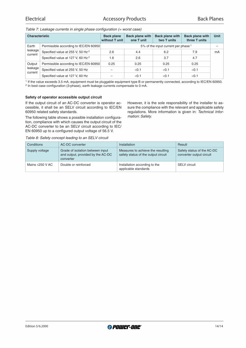
Electrical Accessory Products Back Planes
Edition 5/6.2000 14/14
Table 7: Leakage currents in single phase configuration (= worst case)
Characteristic Back plane Back plane with Back plane with Back plane with Unitwithout T unit one T unit two T units three T units
Earth Permissible according to IEC/EN 60950 5% of the input current per phase 1 –leakage Specified value at 255 V, 50 Hz 2 2.6 4.4 6.2 7.9 mAcurrent
Specified value at 127 V, 60 Hz 2 1.6 2.6 3.7 4.7
Output Permissible according to IEC/EN 60950 0.25 0.25 0.25 0.25leakage Specified value at 255 V, 50 Hz – <0.1 <0.1 <0.1current
Specified value at 127 V, 60 Hz – <0.1 <0.1 <0.1
1 If the value exceeds 3.5 mA, equipment must be pluggable equipment type B or permanently connected, according to IEC/EN 60950.2 In best case configuration (3-phase), earth leakage currents compensate to 0 mA.
Table 8: Safety concept leading to an SELV circuit
Conditions AC-DC converter Installation Result
Supply voltage Grade of isolation between input Measures to achieve the resulting Safety status of the AC-DCand output, provided by the AC-DC safety status of the output circuit converter output circuitconverter
Mains ≤250 V AC Double or reinforced Installation according to the SELV circuitapplicable standards
Safety of operator accessible output circuit
If the output circuit of an AC-DC converter is operator ac-cessible, it shall be an SELV circuit according to IEC/EN60950 related safety standards.
The following table shows a possible installation configura-tion, compliance with which causes the output circuit of theAC-DC converter to be an SELV circuit according to IEC/EN 60950 up to a configured output voltage of 56.5 V.
However, it is the sole responsibility of the installer to as-sure the compliance with the relevant and applicable safetyregulations. More information is given in: Technical Infor-mation: Safety.