Embed Size (px)
Citation preview

From Arrays of THz Antennas to Large-Area Emitters Gottfried H. Dohler, Luis Enrique Garcia-Munoz, Sascha Preu, Stefan Malzer, Sebastian Bauerschmidt,
Javier Montero-de-Paz, Eduardo Ugarte-Munoz, Alejandro Rivera-Lavado, Vicente Gonzalez-Posadas, and Daniel Segovia-Vargas
Abstract—Arrays of coherently driven photomixers with antenna (antenna emitter arrays, AEAs) have been evaluated as a possibility to overcome the power limitations of individual conventional photomixers with antenna ("antenna emitters", AEs) for the generation of continuous-wave (CW) THz radiation. In this paper, "large area emitters" (LAEs) are proposed as an alternative approach, and compared with AEAs. In this antenna-free new scheme of photomixing, the THz radiation originates directly from the acceleration of photo-induced charge carriers generated within a large semiconductor area. The quasi-continuous distribution of emitting elements corresponds to a high-density array and results in favorable radiation profiles without side lobes. Moreover, the achievable THz power is expected to outnumber even large AEAs. Last not least, the technological challenge of fabricating LAEs appears to be significantly less demanding.
Index Terms—High power terahertz, photomixers, planar antennas, terahertz (THz), THz arrays.
I. INTRODUCTION
T HIS paper is devoted to photomixing in "large area emitters" (LAEs). This antenna-free approach is motivated
by the attempt to overcome the power limitations imposed on the conventional AE [1], [2] and AE-arrays. In the LAE, the source of the THz radiation is the acceleration of the photo-generated carriers in a permanent electric field, induced in the semiconductor [2]-[4]. This acceleration process typically takes place on a ps- or sub-ps time scale and results in a THz wave emitted by each photogenerated carrier [2]-[4]. The coherent superposition of all the THz waves originating from the THz periodic carrier generation induced by the two beating laser beams, yields a macroscopic THz field emitted by LAEs. Below, we will show in detail that the THz emission by each accelerated individual photo carrier can be interpreted as the emission of a corresponding transient Hertzian dipole with a single elementary
charge. In order to establish the relation to planar antenna arrays, we will discretize the quasi-continuum of such coherent elementary Hertzian dipoles into a (sufficiently dense) array of Hertzian dipoles with correspondingly larger dipole charge. Simple estimates [2] show that the length of these Hertzian dipoles is much shorter than half a wavelength, which turns them into quite inefficient radiating structures. This drawback, however, is over-compensated by a strongly increased dipole charge, resulting from the fact that much higher laser power can be applied to LAEs: Heating by the absorbed laser power and by photocur-rent represents the limiting factor for both AEs and LAEs, particularly at the focal point, since the generated heat is highest there. An increase of the illumination spot size by a factor 10 to 33, e.g., increases the maximum tolerable laser power and, hence, the induced dipole charge, by a factor of 102 = 100 to 33 ss 1000. This corresponds to an increase of the device size from 8 fimtimes'& fim (the dimensions of a typical antenna-coupled device), to 80 /Ltmx80 /^m, or 250 fj,mx250 /j,m. Interestingly, the short dipole length implies even an advantage at higher frequencies compared to AEs. For the latter, the THz power is strongly limited by the RC-roll-off. The radiation resistance Ra of a Hertzian dipole scales with the square of its length and becomes so small, that the RC roll-off frequency shifts to frequencies well beyond the THz range, and is no limiting factor for the LAEs anymore. Apart from the THz power issues, LAEs are very appealing regarding fabrication and operation. LAEs require only very simple processing steps for the fabrication. For the illumination, an expanded large laser spot can be used, whereas AE-arrays require a sophisticated setup for the coherent illumination of the individual AEs and, possibly another demanding mounting process shaping the THz beam by lenses. In this paper, we will focus our attention on the aspects related to the emission of the radiation, rather than on details of carrier generation and transport. Recently, LAEs based on excitation with fs-laser pulses have been successfully demonstrated and very-broad-band high-power THz radiation with spectra ranging from 100 GHz up to several THz has been observed [5]-[9]. Because of this very wide Fourier spectrum of frequencies and, hence wavelengths, a quantitative analysis of these results, however, is complicated. We will see below that this will result in a wide range of radiation patterns, for the different Fourier components. For a laser pulse with a given Gaussian laser spot size of (sufficiently large) width p0, e.g., the high-frequency (short-wavelength) components may turn out quite strongly collimated, whereas the low-frequency (long-wavelength) components may exhibit much wider lobes. Therefore, a theoretical analysis of these experimental results is beyond the scope of our present, more fundamental study. Very recently, CW photomixing with LAEs has been demonstrated for the first time [10]. Recently, the emission of narrowband

pulsed THz radiation from large-area structure was reported by Krause et al. [9]. This represents an interesting approach, which is suitable for combining the increased conversion efficiency of pulsed excitation with the advantages of (nearly) uniform radiation pattern for single frequency generation. In the following we will restrict our study to LAEs based on CW-photomixing and we will find that it represents a very promising approach for THz emitters with high power and excellent beam profile.
This article is organized in the following way. In Section II we will first introduce and quantify the THz generation by the accelerated carriers under photomixing conditions taking into account the appropriate spatially dependent phase. Subsequently, we will discretize the system of homogeneously distributed, coherently radiating elementary Hertzian dipoles into an equivalent discrete array of Hertzian dipoles with increased charge. The density of this array will be chosen sufficiently high in order to avoid artifacts in the radiation pattern due to interference. For LAEs, the orientation of the transient dipoles depends on the scheme used for the acceleration of the photo-generated carriers. Both, LAEs based on transport parallel to the semiconductor surface, as well as normal to it is possible and will be discussed. In both cases, the radiation pattern of a Hertzian dipole substantially differs from the well-known profile obtained in vacuum or in a uniform dielectric medium, as it is placed at the interface between vacuum and dielectric medium. This will be achieved by a rigorous analytical calculation of the electromagnetic field components at the interface in Section III. As the dipoles emit zero power along their axis, it is clear that conditions for the most favorable radiation patterns will differ strongly for the two transport schemes. Therefore, they will be treated in Sections IV and V separately. In the final Section VI, we will summarize, compare and assess the potential of the different approaches.
II. BASICS OF CW PHOTOMIXING WITH LAES
AEs can be very efficient THz emitters, provided the incoming optical power Pi, is efficiently transformed into a THz AC current JTHZ- In p-i-n photomixers, a responsivity close to the ideal value TV = ITHZ/-PL = e/hvQ (implying that each incoming photon of energy hv^ contributes one elementary charge e to the photo current JTHZ) c a n be achieved, at sufficiently low THz frequencies (up to about 100 GHz). Due to the antenna resistance, of the order of Ra = 70 il [1], [2], one can approach an ideal conversion efficiency of ri&nv = PTHJPL = l/2Ra(e/hv0)
2PL («27.3% at PL = 5 mW, for telecom laser wavelength of, e.g., 1550 nm). In practice, however, much lower THz power is obtained because of the RC roll-off and the transport roll-off, which strongly reduces the THz current fed into the antenna at higher frequencies. In photoconductive photomixers, the responsivity is far below the ideal value, because of the low photoconductive gain, resulting in strongly reduced currents, even at low frequencies. Unfortunately, the small active area of the AE, required to minimize the RC roll-off, imposes strict limits to the maximum tolerable laser power. Focusing the laser beam onto a very small area, results in strong heating [2]. Apart from that, increased laser power yields high photo-carrier densities, which are screening the applied DC electric fields [2] required for their transport.
Much higher total laser power can be applied without the risk of thermal failure and without causing screening if an al-
Intensity
1UWWWUM
-Substrate
" b) Intensity
Fig. 1. Schematic diagram illustrating the principle of photomixing in large area emitters (LAEs). The orientation of the constant electric field (indicated by faint arrows), can be (a) vertical or (b) horizontal. The dipole density is indicated by the black arrows and it is proportional to the intensity distribution in the laser beam. To avoid destructive interference between carriers accelerated in opposite directions every other stripe between the contacts has to be blocked (B) for charge carrier generation by an opaque mask. The dipole length is determined by the short lifetime of the material and of the order of tens of nm.
tentative THz emitter concept is found that allows for the laser power to be spread over a large area comparable with the size of a typical antenna, or even larger. Such a "large area emitter" (L AE) concept [Fig. 1 (a) and (b)] can be implemented by taking advantage of the fact that the charge carriers generated in the semiconductor become elementary Hertzian dipole sources of THz radiation, if subjected to an accelerating DC electric field E D C - The THz fields of the dipoles interfere constructively and the radiated power increases quadratically with laser power. This dependence is identical to the case of antenna emitters as long as the illuminated area is small compared with the THz wavelength [2]. In this case, the angular distribution of the THz power will be the same as that for an elementary dipole ["large area quasi-dipole" (LAQD)]. If, however, the size of the illuminated area becomes comparable with the THz wavelength or even larger, interference effects will become essential (in the far field) and the radiation pattern will become more narrow like in an array of THz antennas. We will find that the maximum radiation intensity still increases quadratically with laser power for the direction of coherent superposition. The total THz power, however, increases only linear with the laser power as the beam width decreases in the limit of a very large area or array
(P0 > ATHz) A single electron in a semiconductor of dielectric constant
esc, characterized by an effective mass mc (typically mc w (0.04 . . . 0.07) mo, where mo = 9.1 x 10 - 3 1 kg is the mass of a free electron), emits a THz pulse if accelerated by an electric field E D C - The total THz power PTHZ(*) is given by [l]-[4]:
THz (*) U'TJ Ht)}2
(1)

Here, e — 1.602 X 10 C is the elementary charge, c — 3 X 101 0 cm/s the vacuum velocity of light, ZQ = (eoc)^1 = 377CI the impedance of free space and nac = (e8C) the refractive index of the semiconductor). In typical III-V semiconductors and at sufficiently high electric fields (>3 kV/cm) the time dependent acceleration a(t) can be approximated by an initial "ballistic" acceleration a i = eEnc/mc up to a maximum ballistic velocity of about v^j* « 108 cm/s (in GaAs) and 2 x 108 cm/s (in InGaAs, e.g.), followed by a deceleration due to scattering, which can be approximated by a2 = —ai [2], [11]. The superposition of the transient THz fields of the carriers generated by the modulated laser power -PL(£) yields in the LAQD-limit
^THz = 9 ' ^ L A Q D ' I THz(<*>THz)| (2)
with
i*LAQD = ( H r ^ } ( ^ f J' = 2 • • • 12-8) • 10 3Q> f o r ^ a i = ( 1 . . . 2 ) - 1 0 8 c m / s (3)
JTHZ(WTHZ) = -fo.pin • / ( W T H Z ) (4)
The frequency dependent factor
/ ( W T H Z ) = ( i - 0 0 6 ( 0 ^ - n . , ) ) ( 5 )
WTHz - 7"bal
increases linearly with WxHzibai at low frequencies, reaches the maxima at about WTHz^bai ^ (3/4)7r and (2n + 1)TT and the minima at WTHz7"bai ~ 2n7T (n — 1 ,2 ,3 , . . . ) . In other words, at low frequencies (WTHZ "C 7"bai)> ^n e ^Hz field contribution of accelerated carriers are strongly reduced due to destructive interference with the opposite field contribution of decelerated, previously generated carriers, as the acceleration and deceleration times, Tbai ~ ^bai/fli = UbaiTOc/e^DC, are short compared to the THz period, TTHZ = I / W H Z - The main maximum
of / ( W T H Z — 37r/4rbai) « 0.72 occurs close to the frequency I'bai at which the acceleration and deceleration times closely correspond to half a THz period TTHZ • The ballistic acceleration time Tbai = ^bai/a = ^bai"ic/e.EDC can be adapted to fulfill the condition for maximum THz power, TTbai — ( 3 / 8 ) T T H Z . — (3 /8 I /THZ)-This condition yields 6 kV/cm < .EDC < 60kV/cm for 0.5 THz < z/THz < 5 THz for InGaAs, e.g., For the optimum adapted fields the THz power becomes
^THzQD = ^ ( l - 7 6 . . . 6 . 7 ) . 1 0 - 3 n . / p2
i n ,
forvbai = ( 1 . . . 2 ) -10 8 cm/s (6)
The angular dependence of the radiation intensity, i.e., the power emitted per solid angle d f2 — sin 8 dd dip, is the same for a LAQD as for a Hertzian dipole in the far-field. It increases quadratically with the sine of the angle between the accelerating DC-field E D C and the vector r from the center of the LAE device to the observation point. For a field in z-direction, E D C = E-DC (0, 0, 1), this angle is identical with the polar angle 8 and one obtains from (2) for the radiation intensity
^ L A Q D W=(^)- J P TL Hz Q D -s in 2 W (7)
whereas, for a field in x-direction, E D C — -EDC 0> 0= 0) the radiation intensity depends on both the polar angle 8 and the azimuth angle ip
UtAQD(0, V) = ( i ) • PTL£Z
QD • (1 - sin2(0) • c o s V ) )
(8)
with P T H ? D f r o m (2)-(6)-The previous considerations apply to a (hypothetical) large
area quasi dipole (LAQD) embedded into an infinite bulk semiconductor. In a typical scenario, however, the absorption of the laser radiation will take place in the semiconductor close to its interface to air at z = 0. The radiation pattern of Hertzian dipoles placed in a semiconductor close to the surface (distance ZQ <tC A) is expected to differ significantly from the one embedded within the infinite bulk. Therefore, in the following Section III, the angular power distribution for the case of a vertical and horizontal Hertzian dipole at the interface to air, ?/^AQD ' l f(0), and for the case of a horizontal dipole, ^fc A Q (0- <f)/dSl, will be developed.
In order to fully take advantage of the large area emitter (LAE) concept, the dimensions of the illuminated area will typically be chosen comparable with the THz wavelength (in the semiconductor), Ao/n s c , or even larger. In this case, interference effects will influence the angular dependence of the radiation pattern. This situation is being treated in Sections IV and V for the two field orientations. In order to establish the close connection of such LAEs to the antenna emitter arrays (AEA)s we will first subdivide the actual "continuous array" of elementary Hertzian dipoles into a discrete, but sufficiently dense array of Hertzian dipoles of correspondingly enhanced dipole charge, yielding an array factor for large area emitters, A F L A E ( P O ) 9, </?), depending on their characteristic dimension, PQ. The actual angular dependence of the radiation intensity at vertical DC E-fields, U^AE{8,ip), and in-plane DC E-fields, U^AE(6, (p), will then be given by the product of the angular dependence of the (modified) Hertzian dipole patterns and the array factors
[ t f A E ( 0 , V) = U ^ ^ i d , V) • AF^AE(8, <p) (9)
U^AE{8, tp) = E/„LAQD<if(0) • AFhAE{8, tp) (10)
respectively.
III. HORIZONTAL AND VERTICAL DIPOLE AT THE INTERFACE
BETWEEN SEMICONDUCTOR A N D A I R
Equations (7) and (8) express the power distribution for vertical and horizontal LAQDs located in an (infinite) semicon-
1/2
ductor with refractive index nsc = eSc (w3.6, e.g., for InGaAs). If the LAQD is located at a distance ZQ far away (ZQ 3> ATHZ) from the interface to air (n — 1), the interference between the directly emitted components (0 < 6 < 7r/2) and the corresponding components emitted under the angle 8' (0 < 8' < 7r/2) and reflected under the same angle 8 has to be taken into account (see Figs. 2 and 3). For 8' exceeding the critical angle for total reflection 6C — a rcs in ( l /n s c ) (wl6° for nsc = 3.6, e.g., for InGaAs) the absolute value of the reflected component becomes unity, |r s c /a i r(^c < 8' < 7r/2)|2 = 1, but

n AIR Y
~^e, X „
i
nsc ;
VI \ / 8' e Z0 / P* rsA/
1 > 8 | f t \
TZ
Fig. 2. Illustration of direct, reflected, and transmitted beams for a vertical LAQD at a distance Za below the xy-plane (interface to air). Because of radial symmetry a consideration in the xz-plane is sufficient. For 0 < 9' < 9C, a transmitted beam exists (blue), for 8c < 0' < TT/2 total reflection occurs (red).
n AIR v
~^e, x w
nsc VI 6' 6
zo / X ^ T A /
_ _ 9 T \ \
TZ
(a)
TZ
(b)
Fig. 3. Illustration of direct and reflected beams for a horizontal LAQD in x-di-rection at a distance z0 below the xy-plane (interface to air). The radiation pattern now depends also on the azimuth angle <p and a 3-dimensional consideration is required, (a) XZ-Plane, and (b) YZ-Plane.
the phase is changing as a function of 8'. The power distribution is determined by the square of the sum of the direct and the reflected field components. For 8' — 8 = 7r/2, in particular, the phase difference between the direct and the reflected component is 7r. Therefore, no power is emitted in the direction parallel to the interface, due to destructive interference. For 6' < 8c,a fraction of the THz power is transmitted into the air. Because of the small value of 8C this fraction, however is very small.
We have derived analytic expressions for the radiation pattern of vertical and horizontal LAQDs located in the semiconductor at small distances (0 < ZQ < ATHZ) from the interface to air. The results are similar to the ones presented in [12]—[15]. The
rigorous mathematical method is presented in [15]. The main results are summarized in the following.
As the radiation intensity for the vertical dipole, U^'A(^D(9) from (7) exhibits radial symmetry, it is sufficient to consider only its dependence on the polar angle 6 in the xz-plane (Fig. 2). The waves emitted by the dipole and reflected at the semiconductor/air interface (and possibly transmitted) are labeled "p-polarized" (p-), as the electric field vector is parallel to the plane of incidence in the far-field. For the horizontal dipole (assumed to be aligned in x-direction), the radiation intensity, Uh (8, ip) from (8), also depends on the azimuth angle, ip (counted from the x-axis) (Fig. 3). The direct, reflected and transmitted waves propagating at any angle 6 in the x-z plane (ip — 0; "E-plane") are p-polarized also for the horizontal dipole, whereas for waves propagating in the y-z plane (<p — 7r/2; "H-plane") the electric field vector in the far-field is perpendicular to the y-z plane. They are labelled as "s-polarized". For an arbitrary angle ip, the radiation field is a superposition of p- and s- polarized waves. At the semiconductor/air interface, z = 0, the transmittance and reflectance TP,RP and Ts,Ra of the p- and s-polarized waves, respectively, are determined by the corresponding Fresnel boundary conditions and by the condition that the power emitted in the semiconductor under the polar angle 9 into the solid angle dQ, — sin 9 d9 dtp is related to the power transmitted into the air under the refraction angle 9t into the corresponding solid angle d flt — sin 8t d8t dip by
{< LAQD (8t)Y • sin{8t) • d8t • dp
= Tp{9) • (E/„LAQD(0))P -sm8-d8- dip (11)
for the vertical large area quasi-dipole and
(u^QB(9t,ip)y •sm(8t)-d8t-dip
= T\8)- (ylAqx>{9,ip)X • sin8-d8-dip, i = a,p (12)
for the horizontal large area quasi-dipole. The refraction angle 8t follows from Snell's law, i.e.,
sin(0t) = nsc • sin(0'), for 8' < 8C
Tp(0) and Ts(0) are given by
4 • nsc • cos(0) • cos(0t) (cos(0) + nsc • cos(8t))
2
4 • nsc • cos(8) • cos(9t)
rjrp
A. Case 0 < 8 < 8C
(n8C • cos(8) + cos(8t))2 '
(13)
(14)
(15)
In this case, the angular distribution of the transmitted power for a vertical LAQD, located in the semiconductor at the interface to air is
(«Cw,«.))'-(i^) ^THzQD-cos2(0f)-sin2(fl) n sc • (cos(0) + n s c • cos(0t))
2 ' (16)

pLAQD THz c o s 2 H - c o s 2 ( e ) - n L - ( n L s i n 2 ( e ) - l )
(n2c-l).[(l + n2
c)-sm2(9)-l] 2 . cn-n^f//^ . r*f\o^( jLAQD
THz P^u-nt'Sm2(ip)-cos2(6)
(n2c ~ 1)
(23)
(24)
Similarly, for the horizontal LAQD at the interface one obtains
«Q D ' i f(M)P
3 \ PTHZQD • cos2(flf) • cos2(fl) • cos2(y>) (£) (17) rasc • (cos(0) + nsc • cos(9t))
2
for the p-polarized component and
P ^ D . c o s 2 ( » « ) . s i n 2 ( r t (^-'M'K^) ^ac • (™Sc • COS(0) + COs(0 t))2
(18)
for the s-polarized one. The power radiated into the semiconductor is determined by
the superposition of the directly emitted wave (0 < 9 < 7r/2) and the corresponding wave emitted under the corresponding angle 9' and reflected at the interface. For the vertical LAQD and for 9 < 9C the power is found to be
<TT™V>*(f>W*=(J-\ PTHzQD-cos2(fl)-sin2(fl)
K"v,.c V)) y2^J (cos(0) + n sc • cos(0t))2 ' (19)
For the horizontal dipole at the interface the power distribution becomes also yj-dependent and one obtains for the p-polarized component
3 ^ ^THzQD • "L • cos2(0) • cos2{9t) • cos2(y>) "(£) (cos(0) + nsc • cos(9t))2
jLAQD o . „„ Q 2 n2c-cos2(9)-smz{<p)
(20)
(21) (nsc • cos(0) + cos(0t))2
for the s-polarized one.
B. Case 9C < 9 < TT/2
If the polar angles 9 and 9' exceed the critical angle for total reflection, there are no transmitted plane waves, as the wave vector in air becomes imaginary. The absolute value of the reflection coefficients becomes unity, but there is a polarization-and angular-dependent phase delay Sp and 8s, respectively, between direct and reflected waves, i.e., r p — exp[j6p(9')] and rs — exp[j6s(9')]. Specifically, for 9' — 90° the phase delay becomes IT for p- and s-polarized waves. Therefore, the direct wave and the reflected wave interfere destructively, independent of the distance of the dipole from the interface and the power
distributions exhibit a zero for the components radiated parallel to the interface.
The radiation intensity radiated into the semiconductor by a vertical LAQD at the interface is found to be
(f™D<"(8))"
\2TTJ (^
^THzQD-«,s2(0)-sin2(0) ( n 2
c - l ) . [ ( l + n 2c ) . s i n 2 ( 0 ) - l ]
(22)
For the horizontal dipole at the interface the radiation intensity for the p-polarized component becomes (23) and (24), shown at the top of the page, for the s-polarized one.
At 9 = 9C the radiation intensities (C/££QD,if (0, tp))' (with i — p,s and j — v, h) are continuous. For the vertical dipole it exhibits its maximum intensity at this angle [see (19) and (22)]
W'"(«J)' -(r;)-'«fD-- ,w-(5?j) pLAQD
r T H z " (25)
due to constructive interference. This value corresponds to 4 times the value emitted at the same angle by a LAQD embedded in an infinite semiconductor. For 9 > 9C, the interference becomes increasingly destructive and \U- s c '' (9, ip)]p
decreases monotonously to zero at 9 = ir/2. For the horizontal dipole [see (21) and (24)] a maximum oc
curs at 9 — 9C in the H-plane (ip — 7r/2)
(£CQD ' i £(0c,^ = V2))S = (3/27r)J ,LAQD THz (26)
due to the constructive interference between direct and reflected wave. This value corresponds to four times the maximum value emitted into the direction perpendicular to the dipole axis by a LAQD embedded in an infinite semiconductor. However, for the E-plane (ip = 0), a zero is obtained according to (20) and (23), due to destructive interference at this angle
« cQ D ' i f ( ^ = o))P = 0. (27)
In Fig. 4, the radiation intensities for (a) the vertical and (b) the horizontal LAQD at the interface are shown (full and dashed lines) and compared with those of the corresponding LAQD embedded in the semiconductor (dash-dotted and dotted lines), renormalized to the maximum power emitted by the dipole embedded into the semiconductor in the direction perpendicular to its axis. The effect of the interface is most pronounced for the vertical dipole [Fig. 4(a)]. As expected, most of the power is emitted into the semiconductor. Its total emitted power is strongly reduced compared with the embedded dipole. The radiation intensity radiated into the semiconductor, t/^A.QD,lt(#)p, exhibits a pronounced maximum at the critical angle for total
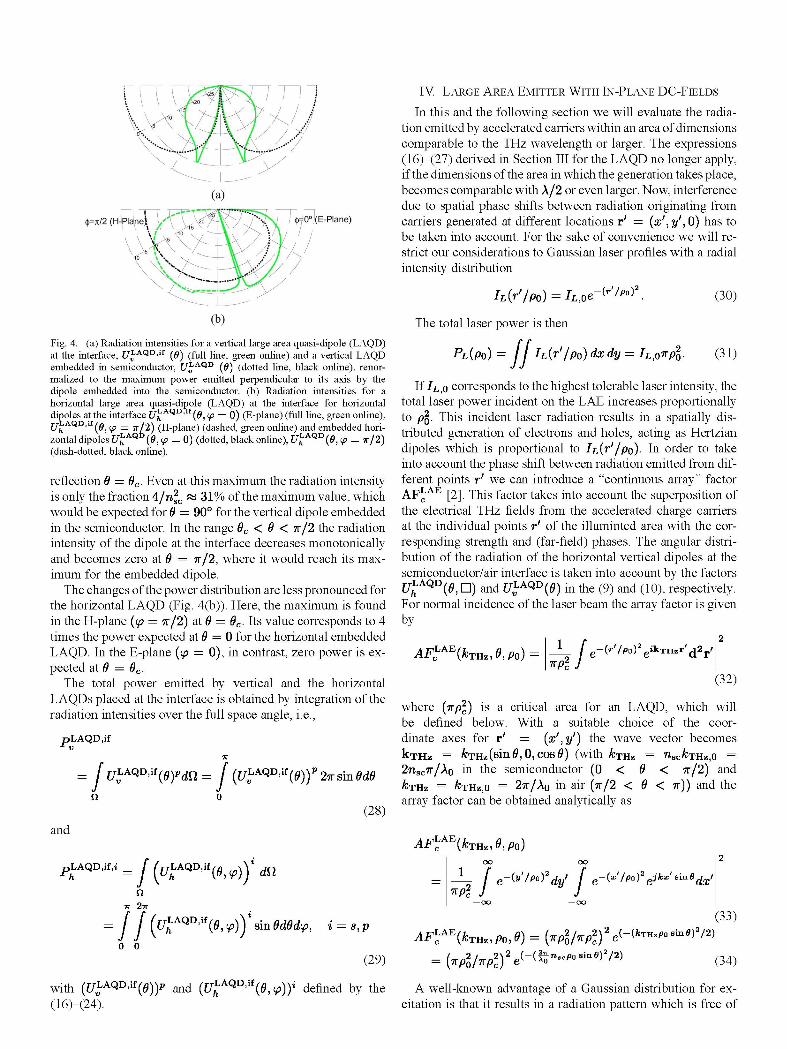
«,=%I2 (H-Plane; c|>=0° (E-Plane)
Fig. 4. (a) Radiation intensities for a vertical large area quasi-dipole (LAQD) at the interface, J/'kAQD.if (0) (full line, green online) and a vertical LAQD embedded in semiconductor, J /^AQD ^ (dotted line, black online), renor-malized to the maximum power emitted perpendicular to its axis by the dipole embedded into the semiconductor, (b) Radiation intensities for a horizontal large area quasi-dipole (LAQD) at the interface for horizontal dipoles at the interface Uh '' [0, tp = 0) (E-plane) (full line, green online),
, if = W2) (H-plane) (dashed, green online) and embedded horizontal dipoles U%AQb (0, <p = 0) (dotted, black online), ^ A Q D (9,<p = x/2) (dash-dotted, black online).
reflection 8 — 8C. Even at this maximum the radiation intensity is only the fraction 4/n2
c PS 31% of the maximum value, which would be expected for 8 = 90° for the vertical dipole embedded in the semiconductor. In the range 6C < 6 < TT/2 the radiation intensity of the dipole at the interface decreases monotonically and becomes zero at 8 = TT/2, where it would reach its maximum for the embedded dipole.
The changes of the power distribution are less pronounced for the horizontal LAQD (Fig. 4(b)). Here, the maximum is found in the H-plane (ip = ir/2) at 8 = 8C. Its value corresponds to 4 times the power expected at 8 = 0 for the horizontal embedded LAQD. In the E-plane (tp — 0), in contrast, zero power is expected at 8 — 6C.
The total power emitted by vertical and the horizontal L AQDs placed at the interface is obtained by integration of the radiation intensities over the full space angle, i.e.,
pLAQD.if
= fu^AQD^{8)pdn= f (U^AQD'it(8))P 2Trsm8d8
n o (28)
and
3LAQD,i
Q 7T 27T
= f I (u^AQD:ii{8,ip)Xsin8d8dip, i = a,p
o o (29)
with (UZAQT>'it(9))p and (tffcAQD'if(0, <*>))* defined by the (16)-(24).
IV. LARGE AREA EMITTER WITH IN-PLANE DC-FIELDS
In this and the following section we will evaluate the radiation emitted by accelerated carriers within an area of dimensions comparable to the THz wavelength or larger. The expressions (16)-(27) derived in Section III for the LAQD no longer apply, if the dimensions of the area in which the generation takes place, becomes comparable with A/2 or even larger. Now, interference due to spatial phase shifts between radiation originating from carriers generated at different locations r' — (x1, y', 0) has to be taken into account. For the sake of convenience we will restrict our considerations to Gaussian laser profiles with a radial intensity distribution
IL{r'lpo) = lL,oe-lr'/pa)* (30)
The total laser power is then
PL(PO) = JflL{r'/po) dxdy = IL^pl- (31)
If IL,O corresponds to the highest tolerable laser intensity, the total laser power incident on the LAE increases proportionally to p%. This incident laser radiation results in a spatially distributed generation of electrons and holes, acting as Hertzian dipoles which is proportional to lL(f'/po)- In order to take into account the phase shift between radiation emitted from different points r' we can introduce a "continuous array" factor AFC [2]. This factor takes into account the superposition of the electrical THz fields from the accelerated charge carriers at the individual points r' of the illuminted area with the corresponding strength and (far-field) phases. The angular distribution of the radiation of the horizontal vertical dipoles at the semiconductor/air interface is taken into account by the factors U%AQD(8, • ) and U^AQD(8) in the (9) and (10), respectively. For normal incidence of the laser beam the array factor is given by
AF^At'(bFHx,e,Po) = |7r#
/ < -('•7i"o)2e*kTHzr'd2r/
(32)
where {itpl) is a critical area for an LAQD, which will be defined below. With a suitable choice of the coordinate axes for r ' = (x',y') the wave vector becomes ki-Hz = kTnz(sm8,0,cos8) (with kTHz — nsckTlizfi — 2nsc7r/Ao in the semiconductor (0 < 8 < 7r/2) and forHz = ^THz.o = 27r/Ao in air (TT/2 < 8 < 7r)) and the array factor can be obtained analytically as
AF^(kTHz,8,p0) oo oo
J _ f e-(v'/po)2dy> f e-^'/PofeJk,'sinedxl
KPI J J
(33) _ ^ _ n 2 / „ -2N2 (-(fcTHzposin0)2/2) AFL
cAE(kTHz,p0,8) = {np2
0/np2cYe
= {KPH-KPI)2 e<-<SF""""in9>a/2) (34)
A well-known advantage of a Gaussian distribution for excitation is that it results in a radiation pattern which is free of

higher order interference lobes. For the z-direction (i.e., 6 — 0) the array factor is always given by the square of the illuminated area (ftp2,) and, hence, the radiation intensity increases quadrat-ically with the laser power, according to (9) and (31), if the illumination intensity at the center of the spot, IL:O, is kept constant, i.e.,
U, LAE (fcTHz, Po, 0 = 0,v)= {7rp20/7rp2
c)2 E/,LAQD ' i f (0 = 0, <p)
(35)
For small values po <C (\o/2irnsc) the array factor does not significantly depend on 8, according to (34), and the quadratic increase of the array factor applies to all directions. In this range of po values, also the total emitted power
°THzEf (&THz,A),¥>) 2\2 pLAQD.if I 2 / 2 \ z
DLiAUU,it „ / 2 / 2NZ DLA
= {KPo/'XPc) PTHz,h ~ {KPahPc) -P T H ;
2\2 pLAQD (36)
increases with the square of the illuminated area. With increasing po, however, the array factor becomes increasingly directional with a 3 dB-angle, determined by
-2(2irnscp0 sin93dB/^o) 1/2. (37)
Finally, for po >• (Xo/2irnsc) the 3 dB angle becomes so small that sin(0) can be replaced by 8. The expression (9) for the radiation intensity of the LAE becomes
familiar discrete arrays- one can discretize the expression (33). This yields a (discrete) array factor
AF^(kTHz,p0,6) V ^ e - ( r n / p o ) 2e J k T H z r , ,
„2 L^i
w i t h r n — a{nx,ny)
(nx, ny) = 0, ± 1 , ± 2 , . . . , Int(2p0/a) (42)
and with fcxHz — ^sc^THz.o — 2nsc7r/Ao in the semiconductor (0 < 8 < 7r/2) and fcrHz — &THz,o — 27r/Ao in air (7r/2 < 8 < 7r), as before. It is clear that the pitch for this (fictitious) discrete array has to be chosen sufficiently small. This implies that
1) the "weight-factors" exp{—(rn/po)2} °f neighboring pixels of the array should only differ by small amounts (i.e., a -C Po) a n d
2) the phase delays between neighboring pixels should be small, even at large angles 8 (i.e., a < Ao/4n s c).
If these conditions are fulfilled, the discrete array of (41) is equivalent to the continuous array defined by (33) with A = a2.
With the array factor calculated from (41) and the radiation intensities of the horizontal LAQD at the interface, f/LAQD,if^ ^y a n d ^ L A Q D . i f ^ ^ f r o m ( 1 ? ) t Q ( 2 3 ) ^
radiation intensities of the horizontal large area emitter at the interface, {/£AQD,if ^ ^p a n d ^ L A Q D . f f ^ ^ c a n n Q W b e
calculated
» U%AE(8 = 0) {nfft/vfi)2 e-Mm"">/XaWtl (38)
Here, the radiation intensity of the LAQD has been replaced by its value at 6 = 0, as U^AE(8, <p) does not significantly change within the range where the array factor significantly differs from zero. The integration of C/^AE(6, (p) over the space angle yields for the total power
,LAE,if rTHz,h lfcTHz,/>0 > - / / ' U^(8^)dQ
^^^(8 = 0) MM)2
f e-l2(™"po/Xo)2e2h-ir8d,8 (39)
PTHEJ (^HZ, Po) « [(1/2) M) (A0/nsc)2/ MY
rLAQD,if/ x U^u'lt(8 = 0). (40)
This result shows that the total THz power only increases linearly with the illuminated area for po ^ Ao/27rnsc. The critical Gaussian beam width pc for the transition from predominant quadratic increase to a predominant linear increase is
Pc = _ _ — = 0.3988 • — = 0.112A0 2-K 2nsc nsc
= 33.6^m@lTHz. (41)
Instead of performing the analytical evaluation of the "continuous array factor" and in order to establish a connection to
U, LAE,if {kTHz,PO,0,if)
pLAQD,if (8,<py + pJ;AQD'if(8,<py
xAF^AE(kTHz,p0,8). (43)
Results of calculations with a — 0.2po are shown in Fig. 5. The full lines depict the radiation intensities Uh '' (8, (p = 0) (E-plane) and the dashed lines Uh '' (8,(p = ir/2) (H-plane) for horizontal large area emitters with carrier generation in the semiconductor close to the interface to air and with DC E-field inx-directionforp0 — (0.1,0.2,0.5,1.0,2.0, 5.0)Ao/rasc. This figure illustrates, that in the range po < 0.2Xo/nsc the increase in radiation intensity is about isotropic and, hence the power increase oc Po (i.e., oc P2). For po > 0 .2ATHZ the radiation intensity at 8 — 0 continues to increase oc /9Q (i.e., oc P^), but the pattern narrows, as expected.
Regarding the THz power, the horizontal dipoles are very attractive from the theoretical point of view. Practically, it turns out to be difficult to fabricate efficient LAEs for CW operation with horizontal electric DC-field, allowing for ballistic transport without suffering from field screening due to saturation effects [3]. The saturation problems can be overcome if a semiconductor with short recombination lifetimes is used. This, however, results in non-ballistic transport and strongly reduced values for the radiation resistance in (3). Roughly speaking, the maximum ballistic electron velocity, Vba,], has to be replaced by the saturation velocity, vs, which is by a factor ~ 3 - 1 0 smaller. As the THz power scales with the radiation resistance this implies a reduction by a factor of 9-100 compared with the ideal value of PTHZ (6).
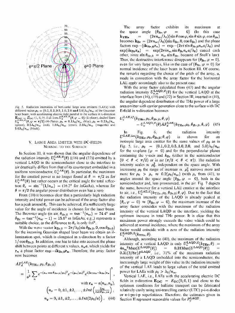
Fig. 5. Radiation intensities of horizontal large area emitters (LAEs) with different radius p0 = (0.1, 0.2,0.5,1.0, 2.0 and 5.0)A0/ragc of the Gaussian laser beam, with accelerating electric field parallel to the surface in x-direction E D C - -EDC (1, 0, 0). Full lines U%AB^(0,ip - 0) (E-plane), dashed lines £^AE,if(0,<P = 1-/2) (H-Plane). p0 = 0.1A0/nBC (blue), p0 = 0.2A0/raBc (green), 0 .5A 0 / J I 3 C (red), 1.0A0/nsc (cyan), 2.0A0/ragc (magenta) and 5.0A0/nBC (black).
V. LARGE AREA EMITTER WITH DC-FIELDS
NORMAL TO THE SURFACE
In Section III, it was shown that the angular dependence of the radiation intensity C/^AE'if (0) ((16) and (22)) emitted by a vertical LAQD in the semiconductor close to the interface to air drastically differs from that of its counterpart embedded in a uniform semiconductor, C/^AE(0). In particular, the maximum for the emitted power is no longer found at 9 = 7r/2 as for U^AE(8) but rather occurs at the critical angle for total reflection 9C = s in _ 1 ( l /n s c ) = (16.2° for InGaAs), whereas for 8 = 7r/2 the angular power distribution even has a zero.
From (10) it becomes clear that a particularly high radiation intensity and total power can be achieved if the array factor also has a peak around 6C. This can be achieved, if a sufficiently large value for the angle of incidence is chosen for the laser beam. The Brewster angle (in air, #Br,o — tan_1(rasc) = 74.4° and #Br = tan_1(rasc — 1) = 15.6° in InGaAs, e.g.,) represents a suitable choice, as the difference to 6C is only 0.6°.
With the wave vector ker,o = 27r/Ao(sin 0Br,O) 0, cos #Br,o) for the incoming Gaussian shaped laser beam we obtain an illumination spot, which is elongated in x-direction by a factor 1/ cos #Br,o • In addition, one has to take into account the phase shift between points at different x values, nxa, which yields for vn a phase factor exp— ikBr,orn Therefore, the array factor now becomes
pLAE AFd (kTUz,PO,SBr,o)
V^ e-(a=™cos0B r . ,o/po)2e-(y™/po)2
e*(kTHz-kBr)r„
n.
ny = 0 , ± 1 , ± 2 , . . . ,
withrn = a(nx,ny),
, ±Int ( —%*—) ,
±Int(2p0/a)y (44)
x - 0, ±1, ±2,..., ±Int (—1^—) ,
The array factor exhibits its maximum at the space angle (9BT,<P = 0) (In this case k-THz — (27rnsc/Ao)(sin^cosy;, sin^sinyj, cos^Br) becomes ksr = (27rnsc/Ao)(sin#BrjO,cos0Br) and the phase factors exp—(ikBr,orn) = exp—(27rzsin0Br,o^ica/Ao) and exp(iksrrn) = exp(27rmscsin^Br^a;a/Ao) cancel each other, since sin#Br,o = nscsm9Bi, because of Snell's law). Thus, the destructive interference disappears for (9BV, f = 0), even for very large arrays, like in the case of (9BT, <P = 0) for normal incidence of the laser beam in Section III. Of course, the remarks regarding the choice of the pitch of the array, a, made in connection with the array factor for the horizontal LAE apply accordingly also to the present case.
With the array factor calculated from (43) and the angular radiation intensity U^^B'if(9) for the vertical LAQD at the interface from (16), (19) and (22) in Section III, inserted in (10), the angular dependent distribution of the THz power of a large area emitter with carrier generation close to the surface with DC E-field in x-direction becomes
U^AE'if(kTHz,p0,8Br,o,e,ip)
= U^'*(9)AF%AE(kTUz, Po, 6Br,0,6, <p) (45)
In Fig. 6, the radiation intensity ULAE<is°(kTHz,p0,0Brt0;6,ip) is shown for an isotropic large area emitter for the same values of po as in Fig. 5, i.e., p0 = (0.1,0.2,0.5,1.0,2.0, and 5.0)A0/rasc
for the xz-plane (ip = 0) and for the perpendicular planes containing the y-axis and &Br (either in the semiconductor (0 < 9 < 7r/2) or in air (ir/2 < 9 < 7r)). The radiation intensity scales oc p^, independent on the space angle. With increasing po the range of increase oc p\ narrows more and more for po > pc PS 0.2(po/nsc) (with pc from (41), to angles around the space angle (9BI,<P = 0), both in the semiconductor and, less pronounced, in the air. Fig. 7 depicts the same, however for a vertical LAE emitter at the interface to air, i.e., ?7^AE,lf(&THZ) POJ #Br,o; @, ¥>)• Due to the fact that the radiation intensity of the LAQD is already peaked at (9c,(p — 0) w (^Br;V — 0), the maximum increase of the array factor coincides with the maximum of the radiation intensity of the vertical LAQD at the interface, yielding the optimum increase in total THz power. It is clear that this maximum power strongly exceeds the value which could be achieved at normal incidence, where the maximum of the array factor would coincide with a zero of the radiation intensity ^ L A Q D , i f ( f e T H z ^
Although, according to (40), the maximum of the radiation intensity of a vertical LAQD is only C/^AQD'if(fcTHz, 0) = 4n-2Max([/LAQD(0)) = O.31Max(C/LAQD(0)) 0 . 3 1 ( 3 / 8 T T ) P L A Q D , i.e., 31% of the maximum radiation intensity of a LAQD embedded into the semiconductor, the increasingly large weight of this value in the radiation intensity of the vertical LAE leads to large values of the total emitted power for LAEs with po > Ao/nsc.
Vertical LAE, i.e., LAEs with the accelerating electric DC fields in z-direction E D C = -Er>c(0,0,1) and close to the optimum conditions for ballistic transport can be fabricated relatively easily using uni-travelling carrier (UTC) p-i-n diodes or n-i-pn-i-p superlattices. Therefore, the estimates given in Section II represent reasonable values for _pLAQD

Fig. 6. Radiation intensities of isotropic LAEs excited by a Gaussian laser beam incident under the Brewster angle (?Br,o with different radius p0 = (0.1,0.2,0.5,1.0, 2.0 and 5.0)A0/raBC. (a)*7L'AE(fcTHz, Pa, ^Br.ol 6,<p = 0) (E-plane), (b) f7LAE(fcTHz, Pa, #Br,o; #Br, ^-Br™>t,r-piBne) (Brewster plane). p0 = 0.1A0/raBC (blue), p0 = 0.2A0/raBC (green), 0.5A0/raBC (red), 1.0A0/raBC (cyan), 2.0A0/raBC (magenta) and 5.0A0/raBC (black).
A comparison of the values of total THz power obtained from both horizontal and vertical LAEs in comparison to AEs and AE-arrays (AEAs) will be given in Section VI.
VI. COMPARISON AND COMMENTS OF THE RESULTS
In this concluding section, we compare the results for large area emitters (LAEs) with those for antenna emitter arrays (AEAs), both regarding the radiation profiles and the total THz power to be expected. We will also comment on the technological feasibility of the two approaches.
Regarding the radiation profiles we notice that large area emitters (LAEs) exhibit only a single lobe with a Gaussian radiation profile reflecting the continuous Gaussian distribution of the radiation sources, whereas antenna emitter arrays (AEAs) exhibit, apart from the main lobe, a more or less large number
Fig. 7. Same as Fig. 6, however, for vertical LAEs, with accelerating electric field normal to the surface (in z-direction) E D C = £ D C ( 0 , 0 , 1 ) . (a) I/£AE ' if(fcTHZ,Po,<Vo;0,¥> = 0) (E-plane), (b) UHA ''f(fcTHz,Po,^Br,o;^Br,^!,-BrewBt0r-pii.n0) (Brewster plane). po — 0.1Ao/nBC (blue), p0 — 0.2X0/n,c (green), 0.5\0/nsc (red), 1.0Ao/raBO (cyan), 2.0Ao/nBO (magenta) and 5.OAo/raBC (black).
of interference-induced side lobes, as the dimensions of the antennas in the range of at least VTKz/2nsc are imposing a minimum pitch for discrete arrays.
In order to reveal the specific properties of AEAs we have performed a detailed analysis of their radiation profiles and the expected power performance [16]. In this work, we studied and compared three fundamentally different versions of antenna emitter arrays:
• AEAs without lens; • AEAs with a large single lens with a radius (much) larger
than the (relatively small) pitch of the array; • AEAs formed by an array of AEs with individual (small)
lenses, optimizing the collimation of the radiation emitted by each individual.

The results can be summarized as follows. • Arrays without lens exhibit a relatively wide radiation pat
tern for smallest reasonable values of pitch a of the array (e.g., a > A0/2nsc).
• The width of the radiation pattern can be reduced and the radiation intensity can be enhanced by the use of a sufficiently large single lens (Si lens with radius, e.g., Ri = 5 mm). The maximum radiation intensity of an (n x n)-array, however, does not reach the ideal value expected, i.e., (n X n)2 times the maximum intensity UAE(8 = 0) of a single AE with lens, as the emission originating from the off-center elements of the array cannot be collimated with the radiation from the central elements.
• Highly sophisticated schemes are required for the coherent illumination of AEAs with small pitch.
• The radiation pattern without lens narrows if the pitch a is increased.
• The problem that the beams from the off-center elements cannot be collimated with the central ones by a lens becomes even more disturbing at increased pitch and the maximum radiation intensity at 8 — 0 becomes much less than its ideal value.
• Coherent illumination of AEAs with increased pitch is easier compared with the small ones, but still extremely demanding in comparison to LAEs.
• The ideal values for antenna emitter arrays with lens, Ufi&(6 = 0) = (n x nfU^{e = 0), can only be achieved, if each AE has its own lens. In this case, however, the central lobe becomes extremely (and for typical applications unreasonably) narrow, because of the large pitch a of the array, determined by the lens radius a = 2Ri (>4 mm, e.g.).
• Coherent illumination of the individual elements of these AEAs remains extremely demanding in comparison to LAEs. In addition, the optical axis of each lens has to be aligned exactly with the corresponding AE.
In Sections IV and V, we have seen that the (Gaussian) array factors become rather narrow already at relatively small values of the Gaussian beam parameters po and the radiation intensity reaches its ideal value. From (34) we obtain an angular dependence of the array factor oc exp[— (6/6sc)
2] with 8SC « 1.8° in the semiconductor and OQ W nsc8sc = 6.45° in air, for Po = Ao = 0.3 mm at 1 THz, e.g., (or, for po = 1 mm even only 8SC — 0.54° and 8o — 1-9°, respectively) at normal laser incidence. Similarly, in Section V, we found for incidence under the Brewster angle (in the case of vertical dipoles at the interface) from (43) that the array factor is very strongly peaked at the Brewster angle in the semiconductor, 0Br,sc (=15.6° in In-GaAs). For angles deviating from the Brewster angle by A8 — 6 — #Br,sc it exhibits again a Gaussian shape. Due to the ellip-tically elongated shape of the illuminated area in x-direction, the value of Qsc is even further decreased by a corresponding factor sinflg1 (=3.73 for InGaAs) for A8 in the xz-plane. These small divergence angles of the THz beam imply that for LAEs no (or only a very simple) THz optical components will be needed for most of the applications.
Considering the much more favorable radiation profiles of LAEs on one side and the demanding challenges associated with fabricating, assembling and coherently illuminating AEAs on
the other side, we come to the conclusion that LAEs, which can be illuminated by a single Gaussian beam and whose fabrication is much simpler, appear, indeed, quite appealing.
As our main goal is to achieve large values of total THz power, the estimated maximum total power expected from LAEs, compared with the values expected from discrete arrays, appears even more important.
In Sections II, IV and V we have derived expressions for the emitted power as a function of Gaussian laser beam parameter po and found two limiting regimes, characterized by po -C pc = (27r)-1/2(A0/2n8C) = 0.056A0 = 0.20A0/2nsc and p0 > pc, respectively (assuming constant laser power for r' — 0). For Po *C pc the total THz power increases oc {irpo)2 and for po ^> pc the total THz power increases oc (7T/92,).
Expressed in terms of the total power emitted by a large area quasi dipole embedded in an infinite semiconductor -PTH3 ((2) to (5)), we obtain from (36) and (39) with U^D,ii(0 = 0) from (23) for the horizontal LAQD at the interface (illuminated under normal incidence)
PTHz,h KkTHz,Po)
= (*($/A)2 i * * 5 i f « (p0/p$rlpmDpc (46) and
PTKz,h {kTHz,Po)
= ( 3 / 2 ? r ) ( p o / P c ) 2 ( ^ % I ) ^ 8 I V p c . (47)
For the vertical LAQD at the interface (illuminated under Brewster angle incidence) we had seen that the power is significantly reduced compared with that of the LAQD embedded into the infinite semiconductor, except for angles close to #BT-,SC
where it is increased by a factor up to 4. This is reflected in the regime po -C pc, where the array factor is isotropic. The space angle integral in (28) yields CP T H ^ with C < 1 and we obtain
PTHz,v (^THz, PO,0Br,o)
— C(kTHz, po, 0Br ,o ) ( /9o / /9c ) 4 fTH? D for PO < Pc- (48)
For the limiting case po >• pc we can use the value for U^AQD{8C) from (25) instead of the value at 0Br, o as an approximation and obtain
THz.v (&THz,A))
= (3/2n)(po/pc)2 {4" V T H Z Q ° f o r p o > P c (49)
Finally, we compare the results for the achievable THz power expected for LAEs with those obtained from AEs. The maximum THz power obtained from real AEs at 1 THz is about 10 p,W [2]. This is about a factor 104 less than the ideal value expected for the case that each photo generated carrier fully contributes to the THz current. In the case of the photoconductive AEs, this discrepancy can be understood, as the photocurrent -fo.ph is by about a factor 100 lowered compared to its ideal value due to the (intentionally) reduced carrier lifetimes, whereas the roll-off factors can be kept rather close to 1 [2]. In the case of

the pin-diode based AEs the DC-photocurrent io.pin is close to its ideal value. The THz current, however, is lowered also by about a factor of 100 due to the roll-off factors [2]. Thus, for both kinds of AEs the THz power can be estimated by
P$&(lTHz) « -Ra [ lO-2J& z(lTffz)]2
«3.5x 10"3 [4dHz(lTffz)]:
(50)
Equation (50) provides nearly the same results for the AEs as does (6) for L AQDs for the case of InGaAs. The area of a L AQD at 1 THz, -Kp\ — 878/^m2, is by a factor of 13.7 larger than that of a typical optimized AE (8 p,m x 8 p,m). This implies that the maximum tolerable absorbed laser power, and, hence, the ideal THz current, I^Hz, is larger by the same factor. The maximum THz power achievable with an ideal (ballistic) L AQD, therefore is expected to be
P^u(lTHz)max » (13.7)2P£fz(lTtfz)m a x » 2mW.
(51)
The conversion efficiency of the LAQD, rjc — P^^^* /Pi,, is increased by a factor 13.7 in comparison to AEs, because of the quadratic relation between THz power and laser power.
For a horizontal LAE with po >• pc we obtain from (47)
PtiUPo, 1™*U « I (£)2 *™W « ( £ ) mW
(52)
and for a vertical LAE from (49)
PTHZ,V(PO, ^THz)umx w 2iml
0.1
Po 2mW
(£)' mW. (53)
As pc (1 THz) =13.7 /zm, the values expected for po = A0/2 are about P%£%h(po, 1 THz))max ta 100 mW or P^^Jpo.lTHz^max « 10 mW. As the conversion efficiency remains constant in the range po > pc, these THz power values require (absorbed) laser power in the range PL < 50 W.
VII. CONCLUSION
We conclude that LAEs promise to outperform antenna emitters (AEs) and antenna emitter arrays in power as well as regarding their radiation profile. Unreasonably large antenna emitter arrays (N = nxxny > 100) would be required to yield THz power in the mW range and the radiation pattern of the AEAs would typically exhibit pronounced side lobes, whereas a single narrow Gaussian lobe is expected for the LAEs. Moreover, their realization is technologically less demanding. Yet we have to be aware that these extremely appealing values are based on the assumption of ballistic transport. This assumption can be fulfilled for the case of vertical LAEs with vertical transport by using p-i-n or n-i-pn-i-p structures. For horizontal LAEs, with their more attractive ideal power values, ballistic transport is much more difficult to be realized. A detailed discussion of the implementation of LAEs is beyond the scope of the present paper.
Very recently, first experimental result on photomixing in large area emitters have been published. The authors are using a LAE configuration with horizontal fields (as in our schematic Fig. 1(b) fabricated from low-temperature-grown GaAs (LT-GaAs)). They claim a THz power of about 2 /jW at 1.2 THz obtained with 900 mW incident laser power (equivalent to ~150 mW absorbed laser power, correcting for 35% reflection loss and 75% loss due to shadowing). As the absorbed laser intensity was at least a factor of 10 less than the maximum tolerable power, the maximum expected THz power is at least by a factor of 10 higher. The authors have also observed the expected narrowing of the radiation profile with increasing laser beam width, as well as steering of the THz beam by changing the angle between the two incident laser beams.
ACKNOWLEDGMENT
The authors also would like to thank D. M. Pozar and D. B. Rutledge for their constructive comments.
REFERENCES
[1] E. R. Brown, K. A. Mcintosh, K. B. Nichols, and C. L. Dennis, "Photomixing up to 3.8 THz in low-temperature-grown GaAs," Appl. Phys. Lett, \ol 66, p. 285, 1995.
[2] S. Preu, G. H. Dohler, S. Malzer, L. J. Wang, H. Lu, and A. C. Gossard, "Tunable, continuous wave terahertz photomixer sources and applications," J. Appl. Phys., vol. 109, p. 061301, 2011, (review article).
[3] J. Larmor, "On a dynamical theory of the electric and luminiferous medium," PMas. Trans. Roy. Soc, vol. 190, pp. 438-461, 1897.
[4] X.-C. Zhang and D. H. Auston, "Optoelectronic measurement of semiconductor surfaces and interfaces with femtosecond optics," J. Appl. Phys., vol. 71, pp. 326-338, 1992.
[5] M. Beck, H. Schafer, G. Klatt, J. Demsar, S. Winnerl, M. Helm, and T. Dekorsy, "Impulsive terahertz radiation with high electric fields from an amplifier-driven large-area photoconductive antenna," Opt. Express, vol. 18, no. 9, pp. 9251-9257, 2010.
[6] A. Dreyhaupt, S. Winnerl, M. Helm, and T. Dekorsy, "Optimum excitation conditions for the generation of high-electric-field terahertz radiation from an oscillator-driven photoconductive device," Opt. Lett., vol. 31, no. 10, pp. 1546-1548, 2006.
[7] M. Awad, M. Nagel, H. Kurz, J. Herfort, and K. Ploog, "Characterization of low temperature GaAs antenna array terahertz emitters," Appl. Phys. Lett, vol. 91, no. 18, p. 181124, 2007.
[8] S. Preu, M. Mittendorff, H. Lu, H. B. Weber, S. Winnerl, and A. C. Gossard, "1550 nm ErAs:In(Al)GaAs large area photoconductive emitters,"^/?/. Phys. Lett., vol. 101, p. 101105, 2012.
[9] J. Krause et at, Opt. Express, vol. 19, p. 19114, 2011. [10] A. Eshaghi, M. Shahabadi, and L. Chrostowski, "Radiation character
istics of large-area photomixer used for generation of continuous-wave terahertz radiation," J. Opt. Soc. Am. B29, no. 4, p. 813, Apr. 2012.
[11] A. Leitenstorfer, S. Hunsche, J. Shah, M. C. Nuss, and W. H. Knox, "Femtosecond high-field transport in compound semiconductors," Phys. Rev. B, vol. 61, no. 24, pp. 16642-16652, 2000.
[12] M. Kominami, D. M. Pozar, and D. H. Schaubert, "Dipole and slot elements and arrays on semi-infinite substrates," IEEE Trans, on Antennas and Propagation, vol. AP-33, no. 6, pp. 600-607, 1985.
[13] D. B. Rutledge, D. P. Neikirk, and D. P. Kasilingam, "Integrated-Cir-cuit Antennas," in Infrared and Millimeter Waves. Vol 10, Millimeter Components and Techniques Part II, K. J. Button, Ed. New York: Academic, 1983.
[14] C. R. Brewitt-Taylor, D. J. Gunton, and H. D. Rees, "Planar antennas on dielectric surface,"Electron. Lett., vol. 12, pp. 729-731, 1981.
[15] W. Lukosz and R. E. Kunz, "Light emission by magnetic and electric dipoles close to a plane interface. Part I. Total Radiated Power. Part II. Radiation pattern of perpendicular oriented dipoles. Part III. Radiation pattern of dipoles with arbitrary orientation," J. Opt. Soc. Amer., vol. 67, no. 12, pp. 1607-1615, 1977.
[16] L. E. Garcia-Mufloz, G. H. Dohler, J. Montero-de-Paz, E. Ugarte-Munoz, A. Rivera-Lavado, S. Preu, S. Malzer, S. Bauer-schmidt, V. Gonzalez-Posadas, and D. Segovia-Vargas, "Internal report of the Universidad Carlos III de Madrid,", unpublished.


![Design of antennas and antenna arrays [ D12 ] - ETH Z](https://img.pdfslide.us/doc/110x75/589ecee61a28ab244d8b5400/design-of-antennas-and-antenna-arrays-d12-eth-z.jpg)