Embed Size (px)
Citation preview
Free-space optical mesh-connected bus networksusing wavelength-division multiple access
Yao Li, Adolf W. Lohmann, and Satish B. Rao
A novel optical free-space mesh-connected bus interconnect network architecture is proposed. Amesh-connected bus [IEEE Trans. Comput. C-30, 264-273 (1981)] is known to have the capability ofinterconnecting, with a three-stage switching, N nodes with a power distribution loss proportional to FNand is therefore advantageous for networking a large number, say over 1000, of communicatingports. Based on conventional space-invariant optical components in a compact and efficient geometry,the proposed optical mesh-connected bus system concept can be used to build either free-space opticalinterconnect links for parallel processing applications or central switching systems for local or globallightwave communication networks. The proposed architecture lends itself to networking under boththe wavelength-division multiple access and other multiple-access environments. In this paper, based onthe wavelength-division multiple-access environment, various optical system implementation andperformance issues are discussed and parameters are analyzed. It was found that by use of a reasonablycompact three-dimensional free-space volume, more than 100,000 dispersion-limited communicationnodes at a uniform channel spacing of 0.75 nm can be linked with a moderate power distribution loss of 28dB. Some preliminary optical wavelength-division multiple-access mesh-connected bus experimentsbased on a 27 x 27 panchromatic optical source array were performed to confirm the operational principleof the proposed concept.
1. Introduction
Fast switching, huge bandwidth, and noninterferingfree-space propagation have been the major drivingforces behind the research on high-throughput opti-cal interconnects for digital computers. A reconfigu-rable optical interconnect, such as a completely con-nected crossbar, is of special interest because of itsnonblocking communication structure capable of pro-viding a large degree of routing flexibility with aminimum reconfiguration time.1 4 It was found,however, that the routing flexibility of an N-process-ing-element (PE) crossbar could be offset by itsserious power drawback, e.g., a power distributionloss (PDL) proportional to N. Although some exter-nal amplification schemes can be used to restore thepower,4 for a large N the signal-to-noise ratio of theamplified outputs may not be tolerable. Based onthis fundamental limit, it was predicted that a cross-
Y. Li and S. B. Rao are with the NEC Research Institute,Princeton, New Jersey 08540. A. W. Lohmann is with Physika-lisches Institut, Angewandte Optik, Staudstrasse 7/B2, D-5520Erlangen, Germany.
Received 8 June 1992.0003-6935/93/326425-13$06.00/0.c 1993 Optical Society of America.
bar can be efficiently implemented only for a moder-ate N, say less than 1000. A second major difficultyfor implementing an optical crossbar is the lack ofefficient optical components for a two-dimensional(2-D) array implementation, so that N PE's have to beplaced along a linear array. In a somewhat differentapproach (a local or a metropolitan network instead ofa crossbar) a pasive star coupler5 6 is used to link Nnodes of communicating ports. There a time-divi-sion multiplexing scheme is furnished. Recentlyfree-space optical star-coupler architectures 7 8 inter-connecting, respectively, a linear and a 2-D array of Nnodes were proposed. Similar to the crossbar, thePDL associated with a star coupler is also propor-tional to N. In addition to the linear access loss, theuse of time-division multiplexing with today's fibertechnology also results in a bandwidth mismatch; i.e.,the bandwidth that a fiber provides cannot be fullyutilized by electronic components. Technology hassomehow remedied this problem by dividing thebandwidth up into channels and having many elec-tronic components communicate over the same fiberconcurrently. This approach is known as the wave-length-division multiple access (WDMA), whose sup-porting devices are tunable optical transmitters andreceivers.9 10 A direct combination of VVDMA withthe star-coupler network can relax the bandwidth
10 November 1993 / Vol. 32, No. 32 / APPLIED OPTICS 6425
requirement on electronic components but still can-not solve the scaling problem, which implies that forcommunicating among N ports, N pairs of suchtunable transmitters and receivers, each with a tun-ing range covering N extinct bands, have to be used.
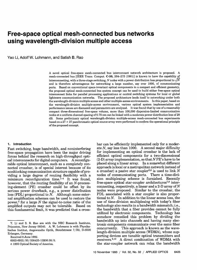
To reduce the interconnect PDL, Wittie introduceda method of decomposition of communication chan-nels. Instead of N ports being placed on a single busfor communication in one step, multiple buses shar-ing the overall communication burden are used in amultiple-step approach. This type of networkingapproach is referred to as a bus-based network;its simplest model is a 2-D mesh-connected bus(MCB) architecture. A MCB of N nodes contains2Fv independent buses, each accessible by INnodes."",12 Figure 1 shows a typical MCB architec-ture in which the two bus arrays are placed perpen-dicularly and each of the N PE nodes is connected toits adjacent row and column buses. Since each bushas a capacity of interconnecting N nodes, a PDL of
N is obtainable at the cost of a three-step time delay.This power-to-time trade-off is advantageous to appli-cations involving a large N, say over 1000, which isvery difficult if not impossible to be supported by anyknown physical system with a single-step reconfigu-rable routing scheme. When a free-space opticalimplementation of the MCB is considered, an addi-tional advantage is that the wiring difficulty thatelectronics experiences is completely avoided. Someof the other known networking properties of the MCBare briefly stated as follows.
While the MCB is more scalable than a crossbar,the crossbar is a more powerful communicationsnetwork. The price we pay, however, for using theMCB architecture rather than a crossbar architecture
Bushl
LM I I mm- LIFig. 1. Architecture of a MCB network interconnecting N PE's,where N = n2. Each of the vertical and horizontal bus arrayscontains n parallel buses.
is not very high at all. For example, any communica-tion pattern that takes a single step on the crossbarcan be routed contention-free on the MCB in threesteps if the pattern is known a priori. 13-15 Evenwithout knowing the pattern ahead of time, we seethat the MCB is still competitive with the crossbarnetwork. To illustrate this, we list the capabilities ofboth the crossbar network and the MCB network inseveral settings.
On-Line Permutation Routing. This is the prob-lem of sending a set of messages in which eachprocessor sends or receives at most one message.Each processor has access to local information only;i.e., it does not know what the destination of anymessage is other than the one it is sending.
* The crossbar network can solve this problemin one step.
* The MCB network with N processors cansolve this problem in O(loglogN) expected time. 4 15
This implies that for any problem the crossbar can doonly a factor of O(loglog N) better than the MCBnetwork.
On-Line h-Relation Routing. This is the problemof sending a set of messages in which each processorsends or receives at most h messages. This models asystem in which the contention is at most h. Thisrequires at least h steps in either model.
* The crossbar with N processors can accom-plish this in O(h + loglog N) steps.'1' 8
* The MCB can accomplish this in O(h + log N)steps.' 4 "18
Off-Line h-Relation Routing. This is the sameproblem as before except that the set of messages isknown apriori. This primitive permits one to stimu-late one step of any fixed-connection fan-out/fan-innetwork in at most h steps. This is a generalizationof the off-line permutation problem.13- 5
* The crossbar network can do this in h steps.* The MCB can do this in 3h/2 steps.
Hypercube Network Simulations. (Hypercube de-rivative networks such as the cube-connected cycleshave similar bounds.)
* The crossbar network can implement a 2d-node hypercube in d steps.
* The MCB network can implement a 2d-nodehypercube in d/2 steps.1315
In light of the superiority of the MCB over thecrossbar for hypercubic networks, the MCB has twotransmitters and receivers at each processor ratherthan one. One could augment the crossbar to havetwo, but again the power dissipation and the numberof channels that are required are doubled, whereas
6426 APPLIED OPTICS / Vol. 32, No. 32 / 10 November 1993
the MCB naturally has a transmitter and receiver forboth the row and the column buses.
In this paper a novel free-space WDMA opticalinterconnect scheme based on a mesh-connected bus(MCB) architecture that possesses a PDL of IN andthat employs only N tunable transmitter/receiverpairs for interconnecting N nodes is suggested. Inaddition to the PDL reduction, the network also lendsitself to interconnecting a high-density 2-D PE array.Various system implementation and performanceissues and some proof-of-principle experiment resultsare discussed.
2. Free-Space Optical Mesh-Connected BusArchitecture
The key components of an N-node MCB network aretwo sets of identical but perpendicularly orientedbuses. Each bus set contains N cross-talk-freebuses placed parallel to each other. Furthermore,each individual bus is accessible by N ports con-nected to it. Optical bus networks have been studiedpreviously.19-22 However, similar to their electroniccounterparts, the existing optical bus schemes weremainly proposed for use in a time-division-multiplex-ing environment. Their physical architecture do notpermit them to be packed densely enough to formarrays of buses to be useful for the MCB applications.The need to satisfy the MCB network requirements
Input pattern
2,1 2,4 1, 2 2,3
3,3 1 4, 1 3,4
1, 4 1 ,3 1 ,1 [4,1]
4, 4 F3 ,2 3 ,1 2, 2
STEP 3
Fii 12 1F-441 4, 4, F[3,1 F21 F23 1
- F_ 3,H
STEP 1
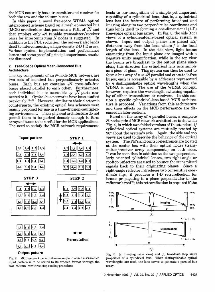
leads to our recognition of a simple yet importantcapability of a cylindrical lens, that is, a cylindricallens has the feature of performing broadcast andimaging along its two perpendicular coordinates andthus lends itself to forming a one-dimensional (1-D)free-space optical bus array. In Fig. 3, the side (top)views of a cylindrical-lens-based optical system isshown. Input and output planes are placed ±2fdistances away from the lens, where f is the focallength of the lens. In the side view, light beamsemanating from the input plane are imaged with anegative unity magnification, while in the top viewthe beams are broadcast to the output plane sincealong this direction the cylindrical lens acts simplyas a piece of glass. This system can thus be used toform a bus aray of n = N parallel and cross-talk-freebuses; each is accessible by n addresses representedby n distinguishable optical wavelengths when theWDMA is used. The use of the WDMA concept,however, requires the wavelength switching capabil-ity of either transmitters or receivers. In this sec-tion a specific cylindrical-lens-based MCB architec-ture is proposed. Variations from this architectureand their effects on the MCB performance are dis-cussed in later sections.
Based on the array of n parallel buses, a completeN-node optical MCB network architecture is shown inFig. 4, in which two folded versions of the standard 4fcylindrical optical systems are mutually rotated by90° about the system's axis. Again, the side and topviews are used to describe the behavior of the opticalsystem. The PE's and control electronics are locatedat the center box with their optical nodes (trans-mitter/receiver array components) on both sides.It can be seen that in addition to the two perpendicu-larly oriented cylindrical lenses, two right-angle orrooftop reflectors are used to bounce the transmittedsignals back to their originating planes. Since aright-angle reflector introduces two consecutive coor-dinate flips, it produces a 1-D retroreflection forbeams propagating in a plane perpendicular to thereflector's roof23; this retroreflection is required if the
bus,bus2
bus,
(a)
bus,,
bussbus,
4,1 4,2 4 ,
E1 EE F,31EPermutation
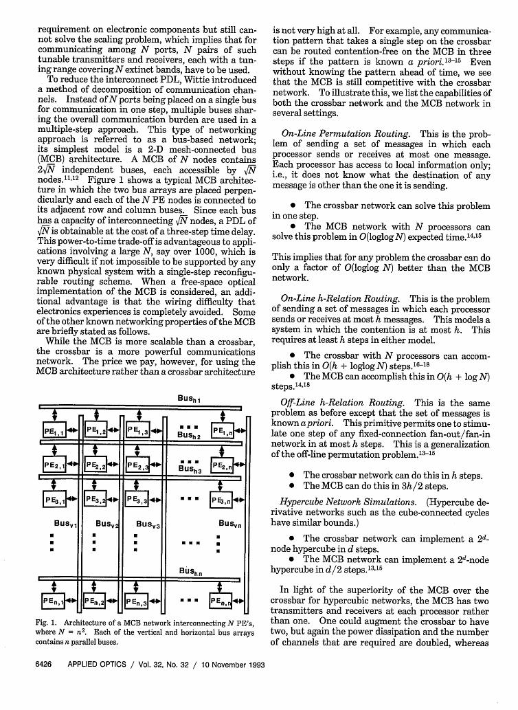
Output patternFig. 2. MCB network permutation example in which a scrambledinput pattern is to be sorted to its ordered format through therow-column-row three-step routing procedure.
X1+- X2+ ... '71
X1+- X2+ *-- An
(b)
Fig. 3. (a) Imaging (side view) and (b) broadcast (top view)properties of a cylindrical lens. When distinguishable opticalwavelengths are used, the lens serves to generate a parallel busarray.
10 November 1993 / Vol. 32, No. 32 / APPLIED OPTICS 6427
1,2 21 2,4 2,3
F3,3 3,4 4,2]4,
4,1 1 I 1, 112, 2 4,4 3,1 3,~2
F IF U
STEP 2
12,2 12,l,4 1 31
3,3 ,
1 4,4 4,2 4,3
Xl
Object Lens, Stop Lens2 ImageTransmitter/receiver array
d
*_ f I f f _ f
d
Transmitter/receiver arraySide View
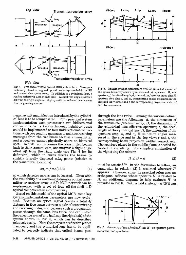
Fig. 4. Free-space WDMA optical MCB architecture. Two sym-metrically placed orthogonal optical bus arrays sandwich the PEand control electronics array. In addition to a cylindrical lens, arooftop reflector is used at each side. A small roof-angle deviationAP3 from the right angle can slightly shift the reflected beams awayfrom originating sources.
negative unit magnification introduced by the cylindri-cal lens is to be compensated. For a practical systemimplementation each processor's two bidirectionalconnections to its two orthogonal neighbor busesshould be implemented as four unidirectional connec-tions, with two sending messages to and two receivingmessages from the two buses because a transmitterand a receiver cannot physically share an identicalspot. In order not to bounce the transmitted beamsback to their transmitters, one may use a slight angleoffset A from the right angle (see Fig. 4 for itsdefinition), which in turns directs the beams toslightly laterally displaced ±Axp points (relative tothe transmitter locations)
Ac = f tan(2AP) (1)
at which detector arrays can be located. Thus withthe availability of a wavelength-tunable optical trans-mitter or receiver array, a 2-D MCB network can beimplemented with a set of four off-the-shelf 1-Doptical components in a compact way.
Based on this model of the optical MCB, some keysystem-implementation parameters are now evalu-ated. Because an optical signal travels a total 4fdistance in free space between a pair of transmittingand receiving nodes, and because such a propagationpasses through the same lens twice, one can unfoldthe reflective arm of any half, say the right half, of thesystem shown in Fig. 5, which can be describedrelatively easily. Here the composite reflection planesdisappear, and the cylindrical lens has to be dupli-cated to correctly indicate that optical beams pass
(a)
Object Projection
7- t
t
I
f * f f I I -(b)
Fig. 5. Implementation parameters from an unfolded version ofthe optical bus array shown by (a) side and (b) top views: D, lensaperture; f, lens focal length; d, transmitter/receiver array size; Haperture stop size; a and at, transmitting angles measured in theside and top views; s and t, the corresponding projection width ofsuch transmissions.
through the lens twice. Among the various definedparameters are the following: d, the dimension ofthe transmitter/receiver array; D, the dimension ofthe cylindrical lens effective aperture; f, the focallength of the cylindrical lens; H, the dimension of theaperture stop; ocs and at, illumination angles mea-sured in the side and in the top view; s and t, thecorresponding beam projection widths, respectively.The aperture placed in the middle plane is needed forcontrol of vignetting. For complete elimination ofthe vignetting the relation
H < D - d (2)
must be satisfied.2 3 In the discussion to follow, anequal sign in relation (2) is assumed wherever Happears. However, since the practical setup uses anorthogonal reflector whose aperture H' is related toH, an additional diagram to help evaluate H' isprovided in Fig. 6. With a field angle uf = d/2f it can
Fig. 6. Geometry of transferring H into H', an aperture param-eter of the rooftop reflector.
6428 APPLIED OPTICS / Vol. 32, No. 32 / 10 November 1993
_-- -, _ at I q *1 * I
Top Vie w
-
be shown that * * .
H cos(uf)H = C2 sin(rr/4 - u) (3)
which implies that, if an aperture equivalent to H isto be maintained, the rooftop reflector's apertureshould be selected as H', and its roof should be placeda distance f away from the cylindrical lens.
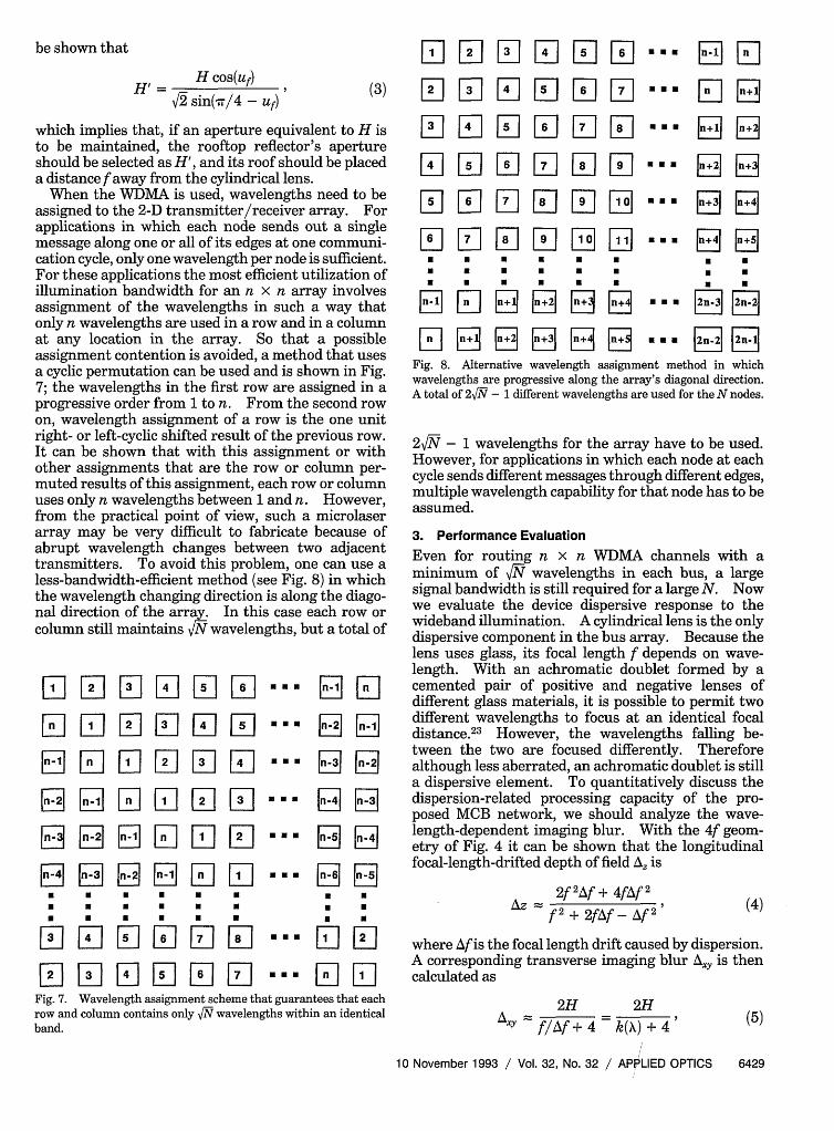
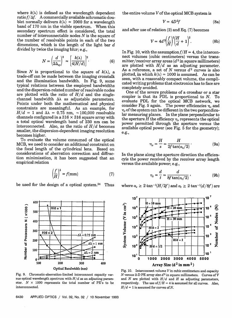
When the WDMA is used, wavelengths need to beassigned to the 2-D transmitter/receiver array. Forapplications in which each node sends out a singlemessage along one or all of its edges at one communi-cation cycle, only one wavelength per node is sufficient.For these applications the most efficient utilization ofillumination bandwidth for an n x n array involvesassignment of the wavelengths in such a way thatonly n wavelengths are used in a row and in a columnat any location in the array. So that a possibleassignment contention is avoided, a method that usesa cyclic permutation can be used and is shown in Fig.7; the wavelengths in the first row are assigned in aprogressive order from 1 to n. From the second rowon, wavelength assignment of a row is the one unitright- or left-cyclic shifted result of the previous row.It can be shown that with this assignment or withother assignments that are the row or column per-muted results of this assignment, each row or columnuses only n wavelengths between 1 and n. However,from the practical point of view, such a microlaserarray may be very difficult to fabricate because ofabrupt wavelength changes between two adjacenttransmitters. To avoid this problem, one can use aless-bandwidth-efficient method (see Fig. 8) in whichthe wavelength changing direction is along the diago-nal direction of the array. In this case each row orcolumn still maintains IN wavelengths, but a total of
Eli-1 ElI5 Eli Eli Eli
H E n E E i4* U n U nF U U U I U1
*- Nn- 2HE-1
I- HE
* - E 2*- N E-3
R*
* U
* N
*El ES
* * * * * U
* * * * * U
* * * * * UM n- F1 Fn nlElE
Fli ElI
*-- EI Ei
*- M tR R
* N* U
* U
*-0 a .- 3U ..- 1
E H H H~~~~~~~ ..*--2 2HiFig. 8. Alternative wavelength assignment method in whichwavelengths are progressive along the array's diagonal direction.A total of 2,rN - 1 different wavelengths are used for the N nodes.
2IN - 1 wavelengths for the array have to be used.However, for applications in which each node at eachcycle sends different messages through different edges,multiple wavelength capability for that node has to beassumed.
3. Performance Evaluation
Even for routing n x n WDMA channels with aminimum of N wavelengths in each bus, a largesignal bandwidth is still required for a large N. Nowwe evaluate the device dispersive response to thewideband illumination. A cylindrical lens is the onlydispersive component in the bus array. Because thelens uses glass, its focal length f depends on wave-length. With an achromatic doublet formed by acemented pair of positive and negative lenses ofdifferent glass materials, it is possible to permit twodifferent wavelengths to focus at an identical focaldistance.23 However, the wavelengths falling be-tween the two are focused differently. Thereforealthough less aberrated, an achromatic doublet is stilla dispersive element. To quantitatively discuss thedispersion-related processing capacity of the pro-posed MCB network, we should analyze the wave-length-dependent imaging blur. With the 4f geom-etry of Fig. 4 it can be shown that the longitudinalfocal-length-drifted depth of field A is
2f 2f + 4fAf2
f 2 + 2fAf - Af 2
where Af is the focal length drift caused by dispersion.A corresponding transverse imaging blur A.,y is thencalculated as
Fig. 7. Wavelength assignment scheme that guarantees that eachrow and column contains only FN wavelengths within an identicalband.
2Hxy t/flf + 4
10 November 1993 / Vol. 32, No. 32 / APPLIED OPTICS 6429
2Hk(X) + 4 (5)
31 F4 -1 61 7]F] F I Fs
where k(X) is defined as the wavelength dependentratio f/Af. A commercially available achromatic dou-blet normally delivers k(k) 2000 for a wavelengthband of 170 nm in the visible spectrum. When thissecondary spectrum effect is considered, the totalnumber of interconnectable nodes N is the square ofthe number of resolvable points in each of the twodimensions, which is the length of the light bar ddivided by twice the imaging blur; e.g.,
(2,)2 [4(H/d) (6)
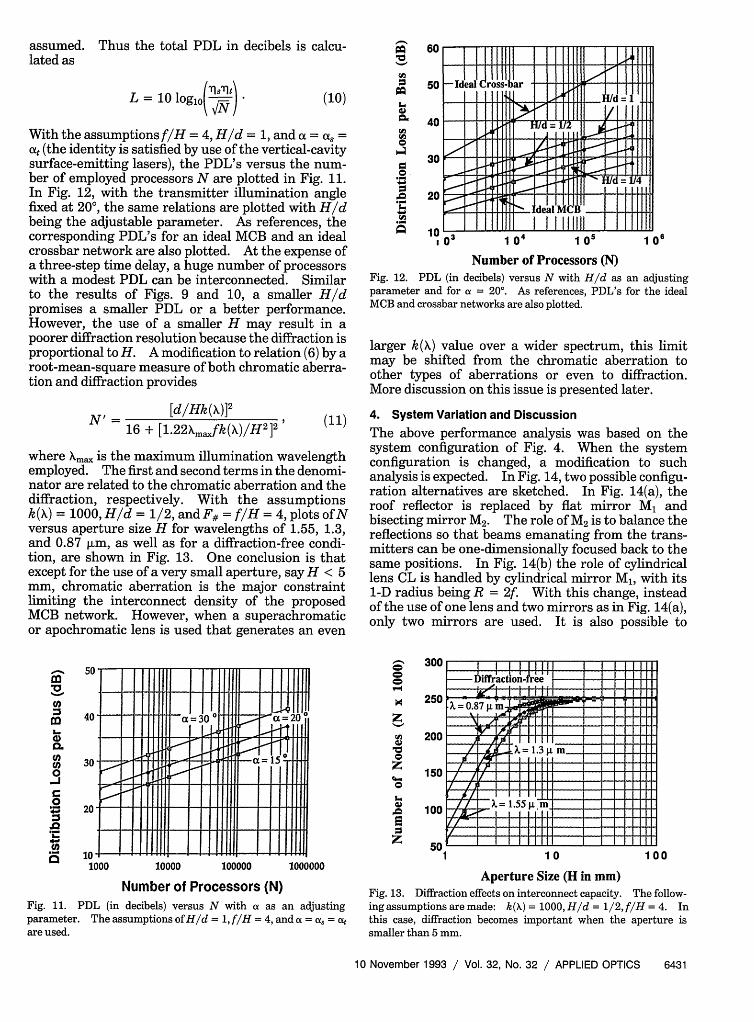
Since N is proportional to the square of k(X), atrade-off can be made between the imaging crosstalkand the illumination bandwidth. In Fig. 9, sometypical relations between the employed bandwidthsand the dispersion-related number of resolvable nodesare plotted with the ratio of H/d and the single-channel bandwidth AX as adjustable parameters.Points under both the mathematical and physicalconstraints are meaningful. As an example, forH/d = 1 and AX = 0.75 nm, 100,000 resolvablechannels configured in a 316 x 316 square array witha total optical wavelength band of 230 nm can beinterconnected. Also, as the ratio of H/d becomessmaller, the dispersion-dependent imaging resolutionbecomes higher.
To evaluate the volume consumed of the opticalMCB, we need to consider an additional constraint onthe focal length of the cylindrical lens. Based onconsiderations of aberration correction and diffrac-tion minimization, it has been suggested that anempirical relation
the entire volume V of the optical MCB system is
V= 4D2f
and after use of relation (2) and Eq. (7) becomes
V = 4d 2H) d +1
(8a)
(8b)
In Fig. 10, with the assumption f/H = 4, the intercon-nect volumes (cubic centimeters) versus the trans-mitter/receiver array areas (d2 in square millimeters)are plotted with H/d as an adjusting parameter.As a reference, a set of N versus d2 curves is alsoplotted, in which k(X) =1000 is assumed. As can beseen, with a reasonably compact volume, the compli-cated writing problems that electronics has to face arecompletely avoided.
One of the severe problems of a crossbar or a starcoupler is that its PDL is proportional to N. Toevaluate PDL for the optical MCB network, weconsider Fig. 5 again. The power efficiencies -i, andmt of the system can be different in the two perpendicu-lar measuring planes. In the plane perpendicular tothe aperture H the efficiency m- represents the opticalpower permitted through the aperture versus theavailable optical power (see Fig. 5 for the geometry);e.g.,
H Hq1s =s 2f tan(as/2) (9a)
In the plane along the aperture direction the efficien-cyis the power received by the receiver array lengthversus the available power; e.g.,
(f 3( u)Y = f(mm)
be used for the design of a optical system.24
(7)
Thus
d dit = = 8f tan(a/2)' (9b)
where a-, 2 2 tan-'(H/2f ) and at 2 2 tan-'(d/8f ) are
200 300
Optical Bandwidth (nm)
107 -- =TO.
ag 106
10 _
a 104 d
.E
cj 102 H/d=
0 1000400
Fig. 9. Chromatic-aberration-limited interconnect capacity ver-sus optical wavelength spectrum with H/d as an adjusting param-eter. N x 1000 represents the total number of PE's to beinterconnected.
Ar
it'll2000 3000 400
ray Size (d 2 in mm2 )
50
6 -106
U,15 sW
0i 4 se-
03 10 6.
02 010 Z
10 1
00
Fig. 10. Interconnect volume V in cubic centimeters and capacityN versus 2-D PE array size d2 in square millimeters. Curves of Vand N are plotted with H/d and H as adjusting parameters,respectively. The use off/H = 4 is assumed for all curves. Also,H/d = 1 is assumed for curves of N.
6430 APPLIED OPTICS / Vol. 32, No. 32 / 10 November 1993
0
x
za0
,oQ
Z
2
0a04-0.0Ez
100
assumed. Thus the total PDL in decibels is calcu-lated as
L = 10 logio / (FNri' (10)
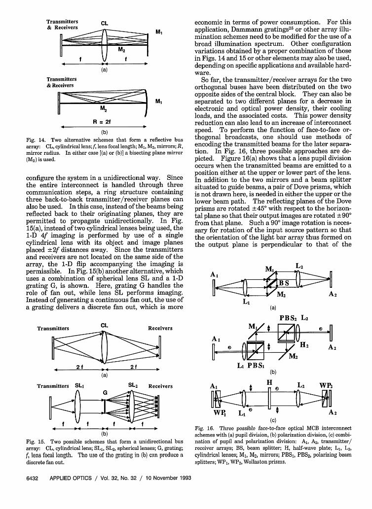
With the assumptions f/H = 4, H/d = 1, and a = a, =a, (the identity is satisfied by use of the vertical-cavitysurface-emitting lasers), the PDL's versus the num-ber of employed processors N are plotted in Fig. 11.In Fig. 12, with the transmitter illumination anglefixed at 200, the same relations are plotted with H/dbeing the adjustable parameter. As references, thecorresponding PDL's for an ideal MCB and an idealcrossbar network are also plotted. At the expense ofa three-step time delay, a huge number of processorswith a modest PDL can be interconnected. Similarto the results of Figs. 9 and 10, a smaller H/dpromises a smaller PDL or a better performance.However, the use of a smaller H may result in apoorer diffraction resolution because the diffraction isproportional to H. A modification to relation (6) by aroot-mean-square measure of both chromatic aberra-tion and diffraction provides
N' =[d/Hk(X)] 2
16 + [1.22Xmafk(X)/H 2 ]2 (11)
where Xma, is the maximum illumination wavelengthemployed. The first and second terms in the denomi-nator are related to the chromatic aberration and thediffraction, respectively. With the assumptionsk(X) = 1000, H/d = 1/2, and F# = f/H = 4, plots of Nversus aperture size H for wavelengths of 1.55, 1.3,and 0.87 jim, as well as for a diffraction-free condi-tion, are shown in Fig. 13. One conclusion is thatexcept for the use of a very small aperture, say H < 5mm, chromatic aberration is the major constraintlimiting the interconnect density of the proposedMCB network. However, when a superachromaticor apochromatic lens is used that generates an even
MU
0uQ
._
0
,0
U,4
60
50
40
30
20
-I _ ar::_:
-_idea I~ eI
10 _l 03 1 o41 of 1 01
Number of Processors (N)Fig. 12. PDL (in decibels) versus N with H/d as an adjustingparameter and for a = 200. As references, PDL's for the idealMCB and crossbar networks are also plotted.
larger k (X) value over a wider spectrum, this limitmay be shifted from the chromatic aberration toother types of aberrations or even to diffraction.More discussion on this issue is presented later.
4. System Variation and DiscussionThe above performance analysis was based on thesystem configuration of Fig. 4. When the systemconfiguration is changed, a modification to suchanalysis is expected. In Fig. 14, two possible configu-ration alternatives are sketched. In Fig. 14(a), theroof reflector is replaced by flat mirror M1 andbisecting mirror M2. The role of M2 is to balance thereflections so that beams emanating from the trans-mitters can be one-dimensionally focused back to thesame positions. In Fig. 14(b) the role of cylindricallens CL is handled by cylindrical mirror Ml, with its1-D radius being R = 2f. With this change, insteadof the use of one lens and two mirrors as in Fig. 14(a),only two mirrors are used. It is also possible to
50co
l
a-1
c0.CoU)03C
._
a-
0
40 1
30
20
'U
1000 10000
0o 11
-
cn
C
4.10
0
4i.',0t- -I 1111111 -|---1-'1 1 10 = 111
100000
11111111
300
250
200
150
100
50
1000000
Number of Processors (N)Fig. 11. PDL (in decibels) versus N with a as an adjustingparameter. The assumptions of H/d - 1, f/H = 4, and a = a, = atare used.
I I I I IiiIbiffrction-ree
0.:C
X= 1.
1 0
Aperture Size (H in mm)
100
Fig. 13. Diffraction effects on interconnect capacity. The follow-ing assumptions are made: k(X) = 1000, H/d = 1/2, f/H = 4. Inthis case, diffraction becomes important when the aperture issmaller than 5 mm.
10 November 1993 / Vol. 32, No. 32 / APPLIED OPTICS 6431
. . . . .............. . . . . .
� I U 111111 I II 111111 i i Um
-I
I
I 111
1 1|11110
TransmittersZ
CL
1I T If
(a)
Transmitters& Receivers
u ~~M2|
R = 2f
(b)
Fig. 14. Two alternative schemes that form a reflective busarray: CL, cylindrical lens;f, lens focal length; M1, M2, mirrors; R,mirror radius. In either case [(a) or (b)] a bisecting plane mirror(M2 ) is used.
configure the system in a unidirectional way. Sincethe entire interconnect is handled through threecommunication steps, a ring structure containingthree back-to-back transmitter/receiver planes canalso be used. In this case, instead of the beams beingreflected back to their originating planes, they arepermitted to propagate unidirectionally. In Fig.15(a), instead of two cylindrical lenses being used, the1-D 4f imaging is performed by use of a singlecylindrical lens with its object and image planesplaced ±2f distances away. Since the transmittersand receivers are not located on the same side of thearray, the 1-D flip accompanying the imaging ispermissible. In Fig. 15(b) another alternative, whichuses a combination of spherical lens SL and a 1-Dgrating G, is shown. Here, grating G handles therole of fan out, while lens SL performs imaging.Instead of generating a continuous fan out, the use ofa grating delivers a discrete fan out, which is more
economic in terms of power consumption. For thisapplication, Dammann gratings25 or other array illu-mination schemes need to be modified for the use of abroad illumination spectrum. Other configurationvariations obtained by a proper combination of thosein Figs. 14 and 15 or other elements may also be used,depending on specific applications and available hard-ware.
So far, the transmitter/receiver arrays for the twoorthogonal buses have been distributed on the twoopposite sides of the central block. They can also beseparated to two different planes for a decrease inelectronic and optical power density, their coolingloads, and the associated costs. This power densityreduction can also lead to an increase of interconnectspeed. To perform the function of face-to-face or-thogonal broadcasts, one should use methods ofencoding the transmitted beams for the later separa-tion. In Fig. 16, three possible approaches are de-picted. Figure 16(a) shows that a lens pupil divisionoccurs when the transmitted beams are emitted to aposition either at the upper or lower part of the lens.In addition to the two mirrors and a beam splittersituated to guide beams, a pair of Dove prisms, whichis not drawn here, is needed in either the upper or thelower beam path. The reflecting planes of the Doveprisms are rotated +45° with respect to the horizon-tal plane so that their output images are rotated ± 900from that plane. Such a 900 image rotation is neces-sary for rotation of the input source pattern so thatthe orientation of the light bar array thus formed onthe output plane is perpendicular to that of the
Al
O L ElF L A 2
(a)
PBS L2
Transmitters CL Receivers
A 2
2f 2f4 - - _-. - -(
(a)
Transmitters SLi
f V f f
SL2 Receivers
f(b)
Fig. 15. Two possible schemes that form a unidirectional busarray: CL, cylindrical lens; SL1, SL 2, spherical lenses; G, grating;f, lens focal length. The use of the grating in (b) can produce adiscrete fan out.
Li PBSi(b)
WPI Li A 2(c)
Fig. 16. Three possible face-to-face optical MCB interconnectschemes with (a) pupil division, (b) polarization division, (c) combi-nation of pupil and polarization division: A, A2, transmitter/receiver arrays; BS, beam splitter; H, half-wave plate; L1, L2,cylindrical lenses; Ml, M2 , mirrors; PBS1 , PBS 2 , polarizing beamsplitters; VWY1, WP2, Wollaston prisms.
6432 APPLIED OPTICS / Vol. 32, No. 32 / 10 November 1993
I
original array; this orientation is needed to performthe orthogonal routings with a set of fixed cylindricallenses. In Fig. 16(b), which shows a polarizationencoding scheme, the two transmitter arrays emitbeams with two orthogonal linear polarizations sothat they can be decoded by the polarizing beamsplitters. Again, the Dove prisms are needed in onebeam path. A second alternative that uses both thepupil and polarization divisions is shown in Fig. 16(c);instead of a polarizing beam splitter, a Wollastonprism is used as a decoding device.
Although a specific performance analysis should becarried out when a specific system configuration isselected, the performance analyses seem to varysystematically. Here, we present a brief discussionon this issue. First, when the object and imageplanes are located ±2f instead of ±f distances awayfrom the lens, the geometrical depth of fields A andA-Y are changed to
4fAff+ f,
4HAf 4HAxy f- Af k(X)
Cs
0
~T44.'
(A
(12)
(13)
respectively. Since for a given k (X) the chromaticblur is now roughly twice the size of the one given bythe system configuration of Fig. 4, its interconnectcapacity or N is reduced by four times.
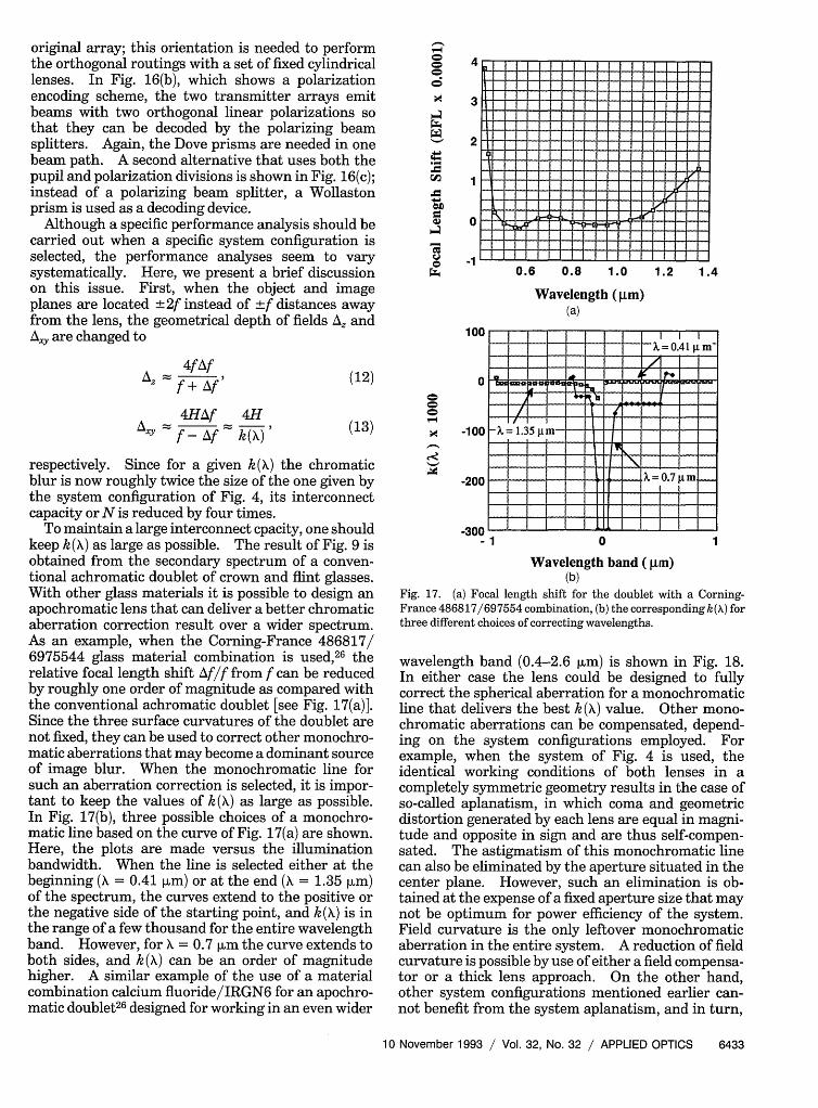
To maintain a large interconnect cpacity, one shouldkeep k(X) as large as possible. The result of Fig. 9 isobtained from the secondary spectrum of a conven-tional achromatic doublet of crown and flint glasses.With other glass materials it is possible to design anapochromatic lens that can deliver a better chromaticaberration correction result over a wider spectrum.As an example, when the Corning-France 486817/6975544 glass material combination is used,26 therelative focal length shift Af/f from f can be reducedby roughly one order of magnitude as compared withthe conventional achromatic doublet [see Fig. 17(a)].Since the three surface curvatures of the doublet arenot fixed, they can be used to correct other monochro-matic aberrations that may become a dominant sourceof image blur. When the monochromatic line forsuch an aberration correction is selected, it is impor-tant to keep the values of k (X) as large as possible.In Fig. 17(b), three possible choices of a monochro-matic line based on the curve of Fig. 17(a) are shown.Here, the plots are made versus the illuminationbandwidth. When the line is selected either at thebeginning ( = 0.41 [lm) or at the end ( = 1.35 im)of the spectrum, the curves extend to the positive orthe negative side of the starting point, and k(X) is inthe range of a few thousand for the entire wavelengthband. However, for X = 0.7 jim the curve extends toboth sides, and k (X) can be an order of magnitudehigher. A similar example of the use of a materialcombination calcium fluoride/IRGN6 for an apochro-matic doublet26 designed for working in an even wider
0CCo
XcI-
14
3-
2 : __ _ _ _ _ _ _ _______
0 - * . * - .- _i_|_______
0.6 0.8 1.0 1.2 1.4
Wavelength (m)(a)
100-X=0.41I~
100 X=l1.35j~a
200 .. .________ 0.7 , _
_ _______
-10 1
Wavelength band (jim)(b)
Fig. 17. (a) Focal length shift for the doublet with a Corning-France 486817/697554 combination, (b) the corresponding k(X) forthree different choices of correcting wavelengths.
wavelength band (0.4-2.6 lm) is shown in Fig. 18.In either case the lens could be designed to fullycorrect the spherical aberration for a monochromaticline that delivers the best k(X) value. Other mono-chromatic aberrations can be compensated, depend-ing on the system configurations employed. Forexample, when the system of Fig. 4 is used, theidentical working conditions of both lenses in acompletely symmetric geometry results in the case ofso-called aplanatism, in which coma and geometricdistortion generated by each lens are equal in magni-tude and opposite in sign and are thus self-compen-sated. The astigmatism of this monochromatic linecan also be eliminated by the aperture situated in thecenter plane. However, such an elimination is ob-tained at the expense of a fixed aperture size that maynot be optimum for power efficiency of the system.Field curvature is the only leftover monochromaticaberration in the entire system. A reduction of fieldcurvature is possible by use of either a field compensa-tor or a thick lens approach. On the other hand,other system configurations mentioned earlier can-not benefit from the system aplanatism, and in turn,
10 November 1993 / Vol. 32, No. 32 / APPLIED OPTICS 6433
-
1
0
-1
-2L
60
40
20
0
-20
An
1 2
Wavelength (gim)(a)
1 .5 A
_ __ __ _ .A_X=0.4glm
-_X2.6 gLm_
- 3 - --3 - 2 - 0 1 2
Wavelength band (gim)(b)
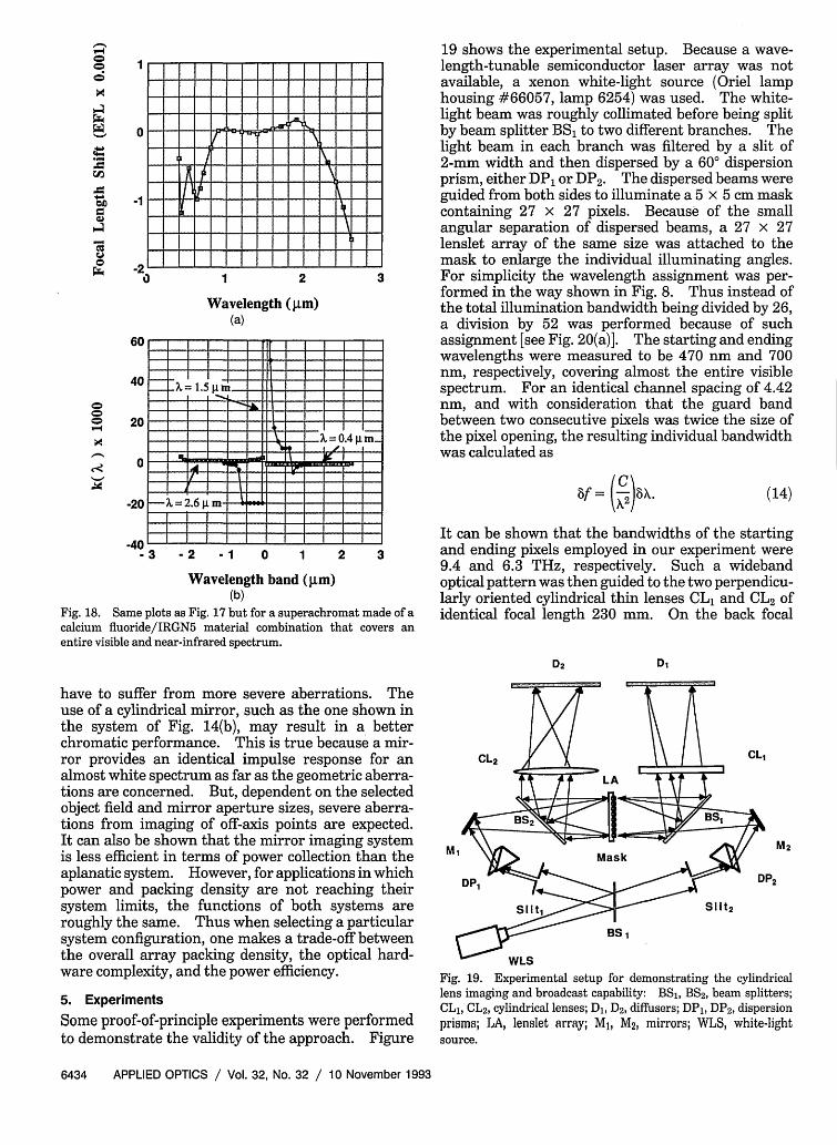
Fig. 18. Same plots as Fig. 17 but for a superachromat mcalcium fluoride/IRGN5 material combination that co,entire visible and near-infrared spectrum.
19 shows the experimental setup. Because a wave-_ length-tunable semiconductor laser array was not_ available, a xenon white-light source (Oriel lamp_ housing #66057, lamp 6254) was used. The white-- light beam was roughly collimated before being split_ by beam splitter BS1 to two different branches. The_ light beam in each branch was filtered by a slit of_ 2-mm width and then dispersed by a 60° dispersion_ prism, either DP or DP2. The dispersed beams were- guided from both sides to illuminate a 5 x 5 cm mask- containing 27 x 27 pixels. Because of the small_ angular separation of dispersed beams, a 27 x 27
lenslet array of the same size was attached to themask to enlarge the individual illuminating angles.
3 For simplicity the wavelength assignment was per-formed in the way shown in Fig. 8. Thus instead ofthe total illumination bandwidth being divided by 26,a division by 52 was performed because of suchassignment [see Fig. 20(a)]. The starting and endingwavelengths were measured to be 470 nm and 700nm, respectively, covering almost the entire visiblespectrum. For an identical channel spacing of 4.42nm, and with consideration that the guard bandbetween two consecutive pixels was twice the size ofthe pixel opening, the resulting individual bandwidthwas calculated as
(f= () x. (14)
:1 It can be shown that the bandwidths of the startingand ending pixels employed in our experiment were9.4 and 6.3 THz, respectively. Such a widebandoptical pattern was then guided to the two perpendicu-larly oriented cylindrical thin lenses CL1 and CL2 of
ade of a identical focal length 230 mm. On the back focalvers an
D2 Di
have to suffer from more severe aberrations. Theuse of a cylindrical mirror, such as the one shown inthe system of Fig. 14(b), may result in a betterchromatic performance. This is true because a mir-ror provides an identical impulse response for analmost white spectrum as far as the geometric aberra-tions are concerned. But, dependent on the selectedobject field and mirror aperture sizes, severe aberra-tions from imaging of off-axis points are expected.It can also be shown that the mirror imaging systemis less efficient in terms of power collection than theaplanatic system. However, for applications in whichpower and packing density are not reaching theirsystem limits, the functions of both systems areroughly the same. Thus when selecting a particularsystem configuration, one makes a trade-off betweenthe overall array packing density, the optical hard-ware complexity, and the power efficiency.
5. Experiments
Some proof-of-principle experiments were performedto demonstrate the validity of the approach. Figure
M
DP2
%_ WLSFig. 19. Experimental setup for demonstrating the cylindricallens imaging and broadcast capability: BS1, BS2, beam splitters;CL1 , CL2, cylindrical lenses; D1, D2 , diffusers; DP1 , DP2 , dispersionprisms; LA, lenslet array; MI, M2 , mirrors; WLS, white-lightsource.
6434 APPLIED OPTICS / Vol. 32, No. 32 / 10 November 1993
-Co
0
.PkW
it
v:
co
0
0
I I I I -
--- - _40
- I I I
I I I-
- / I I I
__L_ I I I I
- I I. LLL1_1
I------ ........
I
Xl= 470 nm* AX = 4.42 nm
11 | - | ! l l I ! l_Z I Xm3e : :,Il I : A::x : , : ' : 1 : Cal
E l5 § b i ' E EE . is= x z . I ; ; ; ; J := 32 . . . . . . x w ; A_led:t l : L ; EGG l 3G.r orr no l r 71 r
= nr r3r : . . : E AS :E 3: TIC i i ; ; ; ; J ;E D: ;GX , i i . . . ; J bi31 ' 91 1 : . :E XI GLi:r r l : - i : E :x L =-1|1 3C 1 if u : : : i : G it GOXl 3C: 1u . i ; . 1 . ;i1GG 1_[!lT} ::C ; ............... i 1 3so ; zE: - . : : 3 : n I IBEX: . , . s . Guy_i i i ' - ' ' R GG i
x x3 a : . : , z ; HEX1: gcG3t.lIID.Z XXxX = . ; . G 2 . Atfig : SacI:Is _ l l l l * l _
X53 =700 nm
optics
electronics
(a)V V VV V V
(a)
\\\Vvv\-
(b)
(b) (C)Fig. 20. Experimental results of forming WDMA bus arrays: (a)a 27 x 27 color point source array with wavelength progressiondirection being along the main diagonal axis of the array; (b), (c) 27horizontal and vertical buses formed after use of two identicalcylindrical thin lenses.
plane of each lens a wideband optical bus array wasformed [see Figs. 20(b) and 20(c)]. Because of theuse of the described wavelength assignment, thewavelength contents in different buses were different,which explains the reason for observable color differ-ences in the bus array. Because of the use of amacroscopic scale, effects of chromatic aberrationwere not severe even for the employed singlet cylindri-
PE1 PE2 PE3 PE4 -u.. PEn
XI X 6X 7 X1 2X13 X18X1 9 X24
Bus,
Bus2
I. OOOO224@OOO-22O @@-Ic °llii11°°°°°1i°°°° 1 °°°e
10- MM1U 1:
Bus3 I|::8°8888ls$ soo8ss:Is
Bus4 r6*0gg :s0::: :::so : 106:1:o
* * U* * U* * X
s 00000 |$$$0000$$$$3$ 0$$$
I. . . . X6n-5 6n
10000001
Ie *e-o-n
U.... 5 _00 0.*e ecee* e* 222
* *ioo 0O
/Wavelength coded
transmitter/receiver array
Fig.21. Transmitter/receiver array containing n x nh individualnode pairs for routing h-relation graphs.
electronics
(c)Fig. 22. Various other bus-based interconnect possibilities:arrays that require (a) two, (b) three, and (c) four interconnectingbuses and their optical layouts.
cal lens. For the same experimental condition, e.g.,the same optical components, for the same bandwidthof the visible spectrum, and for the same array size, itshould not be difficult to double the array densitywhile still maintaining an acceptable signal-to-cross-talk ratio, which can lead to an interconnect capacityof some 3000 ports.
6. Discussion and Summary
As mentioned above, the use of the proposed opticalMCB together with the WDMA requires wavelengthselectivity of either an optical transmitter or a re-ceiver, which is not available at present. Recentresearch on the vertical-cavity surface-emitting semi-conductor quantum-well lasers has shown some en-couraging results; 140 distinguishable narrow-lin-ewidth (0.3-nm) lasing emissions from such laserssituated in a wavelength band of 43 nm have beensuccessfully integrated.27 It should not be too diffi-cult to make a large array with the same bandwidthand the same technology. Thus at least 19,600communication nodes can be linked with the pro-posed MCB network if the same number of receiverscan also be integrated. Other promising device can-didates such as the distributed-feedback and thedistributed-Bragg-reflector lasers are also under devel-opment.2 8'29 As for the tunable receivers, steadyprogress has also been made in terms of both coher-ent detection and direct detection technology.30-33
While coherent detection offers higher detection sen-sitivity than direct detection, the cost of this advan-
10 November 1993 / Vol. 32, No. 32 / APPLIED OPTICS 6435
optics
electronics
'1' 11, '1' %1' 'J., 'V W .
Ix -
\1X1 )0X
7;1I
7
tage is an increase in system complexity. It is be-lieved that, because WDMA efficiently fills the fibercommunication bandwidth without overloading thecapacity of the switching electronics, more and moreeffort will be made to develop tunable optical transmit-ters and receivers that can be integrated.
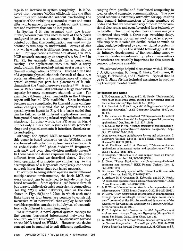
In Section 5 it was assumed that one trans-mitter/receiver pair was used at each of the N portsconfigured in an n x n square array. It should bepointed out that this configuration was used simplybecause it was easy to understand. Arrays of sizen x m, in which m is different from n, can also beused. For applications to route h relations, a WDMAMCB network can employ an array of n x hn (h = 6 inFig. 21, for example) channels for a concurrentrouting. For applications that use such a arrayconfiguration, the speed advantage over a basic n x nchannel configuration is obvious. Instead of the useof h separate physical channels for each of the n x nports, an alternative is the maintenance of a singleoptical channel per port but placement of h sub-channels at the h submicrowave carriers.34 35 A nar-row WDMA channel still contains a large bandwidthcapacity for many microwave channels to use. Forexample, a 0.5-nm optical bandwidth in the 1.55-jimregion still has 50 GHz available. Since hardwarebecomes more complicated for this and other configu-ration changes, it should also be pointed that theoptical system layout in Fig. 4 is a basic model thatcan be tailored to fit different applications rangingfrom parallel computing to local or global data commu-nications. In other words, the PE array in Fig. 4implies only a black box; regardless of its geometricshape and physical contents, it interfaces the electron-ics and optics.
Although the optical MCB network discussed inthis paper is based primarily on the WDMA, it canalso be used with other multiple-access schemes, suchas code-division,36-37 phase-division,38 frequency-division,39 and even time-division multiple access.40
In these cases the device requirements may be quitedifferent from what we described above. But thebasic operational principles are similar, e.g., in thedecomposition of a large-scale completely connectednetwork into a three-stage bus-based network.
In addition to being able to operate under differentmultiple-access environments, the basic MCB net-work concept can be extended to include other bus-based networks. Since optics is used here to furnishbus arrays, while electronics controls the connections[see Fig. 22(a)], other networks, such as the onesshown in Figs. 22(b) and 22(c), in which each nodelinks three or four buses, are possible to construct.Recursive MCB networks4' that employ buses withvariable capacities can also be built by use of transmit-ters with different transmitting angles.
To summarize, a novel optical system concept forthe various bus-based interconnect networks hasbeen proposed in this paper. The discussion focusedon the MCB based on WDMA. However, the deviceconcept can be modified to suit different applications
ranging from parallel and distributed computing tolocal or global computer communications. The pro-posed scheme is extremely attractive for applicationsthat demand interconnection of huge numbers ofnodes and that are otherwise very difficult for conven-tional electronics and even for optical fiber technologyto handle. Our initial system performance analysisillustrated that with a three-step switching delay,such a free-space optical network provides a powerefficiency that is twice (in decibel scale) as much aswhat could be delivered by a conventional crossbar orstar network. Since the WDMA technology is still inits infancy, development of fast-switching narrow-linewidth wide-range-tunability optical transmittersor receivers are crucially important for this networkconcept to beconme a reality.
We acknowledge helpful discussions with J. Kilian,J. A. Giordamaine, K. Lang, R. Linke, Y.-D. Lyuu, B.Maggs, E. Schenfeld, and L. Valiant. Special thanksgo to T. Jiang for his technical assistance in produc-ing the experimental result.
References and Notes1. J. W. Goodman, A. R. Dias, and L. M. Woody, "Fully parallel,
high-speed incoherent optical method for performing discreteFourier transforms," Opt. Lett. 2, 1-3 (1978).
2. A. A. Sawchuk, B. K. Jenkins, and C. S. Raghavendra, "Opticalcross-bar networks," IEEE Computer (October 1987), pp.45-57.
3. A. Hartmann and Steve Redfield, "Design sketches for opticalcross-bar switches intended for large-scale parallel processingapplications," Opt. Eng. 28, 315-327 (1989).
4. A. E. Chiou and P. Yeh, "Energy efficiency of optical intercon-nections using photorefractive dynamic holograms," Appl.Opt. 27, 2093-2096 (1990).
5. Joint special feature on lightwave devices and subsystems, J.Lightwave Technol. LT-3(6), (1985); IEEE Trans. ElectronDevices ED-32(12), (1985).
6. W. J. Tomlinson and C. A. Brackett, "Telecommunicationapplications of integrated optics and optoelectronics," Proc.IEEE 75, 1512-1523 (1987).
7. C. Dragone, "Efficient N x N star coupler based on Fourieroptics," Electron. Lett. 24, 942-943 (1988).
8. R. Linke, "Power distribution in a planar-waveguide-basedbroadcast star network," IEEE Photon. Technol. Lett. 3,850-852 (1991).
9. B. Glance, "Densely spaced WDM coherent optic star net-work," Electron. Lett. 23, 875-876 (1987).
10. E. Arthurs, M. S. Goodman, H. Kobrinski, and M. P. Vecchi,"A broadband optoelectronic packet switching system," IEEETrans. Commun. 37, 645-648 (1989).
11. L. D. Wittie, "Communication structure for large networks ofmicrocompuers," IEEE Trans. Comput. C-30,264-273 (1981).
12. P. Dowd, "High performance interprocessor communicationthrough optical wavelength division multiple access chan-nels," presented at the 18th International Symposium of theAssociation for Computing Machinery on Computer Architec-tures, Toronto, 27-30 1991.
13. F. T. Leighton, Introduction to Parallel Algorithms andArchitectures: Arrays, Trees, and Hypercubes (Morgan Kauf-mann, San Mateo, Calif., 1992), Chap. 1, p. 186.
14. W. McColl, "General purpose parallel computing," in Lectureson Parallel Computation: Proceedings of the 1991 ALCOMSpring School on Parallel Computation, A. M. Gibbons and P.
6436 APPLIED OPTICS / Vol. 32, No. 32 / 10 November 1993

Spirakis, eds. (Cambridge U. Press, Cambridge, 1993), pp.337-391.
15. S. Rao, NEC Research Institute, Princeton, N.J. 08540 (per-sonal communication); see also "Properties of an interconnec-tion architecture based on wavelength division multiplexing,"NEC Tech. Rep. 92009-3-0054-90020 (NEC Research Insti-tute, Princeton, N.J., 1992).
16. R. J. Anderson and G. L. Miller, "Deterministic parallel listranking," in Aegean Workshop on Computing VLSI Algo-rithms and Architectures, J. Reif, ed., Vol. 319 of LectureNotes in Computer Science (Springer-Verlag, New York, 1988),pp. 81-90.
17. L. A. Goldberg, M. Jerrun, F. T. Leighton, and S. Rao, "Adoubly logarithmic communication algorithm for the com-pletely connected optical communication parallel computer,"presented at the 5th Annual Association for Computing Ma-chinery Symposium on Parallel Algorithms and Architectures,Velen, Germany, 28-30 June 1993.
18. L. G. Valiant, "General purpose parallel architectures," inHandbook of Theoretical Computer Science, J. van Leeuwen,ed. (Elsevier, Amsterdam, 1990), pp. 943-871.
19. A. W. Lohmann, "Optical bus network," Optik 74, 30-35(1986).
20. P. Healey, "Minimizing crosspoints and spatial highways inmulti-dimensional bus networks," Electron. Lett. 25, 1515-1517 (1989).
21. P. Healey, S. Cassidy, and D. W. Smith, "Multi-dimensionaloptical interconnection networks," in Digital Optical Comput-ing II, R. Arrathoon, ed., Proc. Soc. Photo-Opt. Instrum. Eng.1215, 191-197 (1990).
22. S. Kawai and M. Mizoguchi, "Two-dimensional optical busesfor massively parallel processing," in Optical Computing, Vol.6 of 1991 OSA Technical Digest Series (Optical Society ofAmerica, Washington, D.C., 1991), pp. 136-139.
23. W. T. Welford, Geometrical Optics: Optical Instrumentation,(North-Holland, Amsterdam, 1962), pp. 67-72.
24. A. W. Lohmann, "Scaling laws of lens systems," Appl. Opt. 28,4986-4988 (1989).
25. H. Dammann and K. Gortler, "High-efficiency in-line multipleimaging by means of phase holograms," Opt. Commun. 3,312-315 (1971).
26. R. I. Mercado, "Correction of secondary and higher-orderspectrum using special materials," in Passive Materials forOptical Elements, G. W. Wilkerson, ed., Proc. Soc. Photo-Opt.Instrum. Eng. 1535, 184-198 (1991).
27. C. J. Chang-Hasnain, J. P. Harbison, C.-E. Zah, M. W. Maeda,L. T. Florez, N. G. Stoffel, and T.-P. Lee, "Multiple wavelengthtunable surface-emitting laser arrays," IEEE J. QuantumElectron. 27, 1368-1376 (1991).
28. Y. Yoshikuni, K. Oe, G. Motosugi, and T. Matsuoka, "Broadwavelength tuning under single-mode oscillation with a multi-electrode distributed feedback laser," Electron. Lett. 22, 1153-1154 (1986).
29. J.-P. Noblanc, "Semiconductor lasers: highlights and trends,"in Optoelectronic Materials and Device Concepts, M. Razeghi,ed., Proc. Soc. Photo-Opt. Instrum. Eng. PM05/HC, 212-221(1991); S. Murata, I. Mito, and K. Kobayashi, "Tuning rangesfor 1.5-p1m wavelength tunable DBR lasers," Electron. Lett.24, 577-579 (1988).
30. R. A. Linke, "Frequency division multiplexed optical networksusing heterodyne detection," IEEE Network (March 1989), pp.13-20.
31. P. E. Green and R. Ramaswami, "Direct detection lightwavesystems: why pay more?" IEEE Lightwave Commun. Syst.1, 36-49 (1990).
32. A. Frenkel and C. Lin, "In-line tunable 6talon filter for opticalchannel selection in high density wavelength division multi-plexed fiber systems," Electron. Lett. 24, 159-161 (1988); L.Stone and L. W. Stulz, "Pigtailed high finesse tunable fiberFabry-Perot interferometers with large, medium and smallfree spectral ranges," Electron. Lett. 23, 781-782 (1987).
33. B. Glance, "Polarization independent coherent optical re-ceiver," J. Lightwave Technol. LT-5, 274-276 (1987).
34. T. E. Darcie, "Subcarrier multiplexing for multiple-accesslightwave networks," J. Lightwave Technol. LT-5, 1103-1110(1987).
35. A. A. M. Saleh, "Fundamental limit on number of channels insubcarrier-multiplexed lightwave CATV system," Electron.Lett. 25, 776-777 (1989).
36. J. A. Salehi, "Emerging optical code-division multiple accesscommunications systems," IEEE Network (March 1989), pp.31-39.
37. A. M. Weiner, J. P. Heritage, and J. A. Salehi, "Encoding anddecoding of femtosecond pulses," Opt. Lett. 13, 300-302(1988).
38. L. J. Cimini, Jr., "Optical phase division multiplexing for localcommunications applications," IEEE Trans. Commun. 37,1282-1292 (1989).
39. I. P. Kaminow, "Noncoherent photonic frequency-multiplexedaccess networks," IEEE Network (March 1989), pp. 4-12.
40. P. Prucnal, M. Santoro, S. Segal, and I. Kaminow, "TDMfiber-optic network with optical processing," Electron. Lett.22, 1218-1219 (1986).
41. J. I. Capetanakis, "Generalized TDMA: the multi-accessingtree protocol," IEEE Trans. Commun. COM.-27, 1476-1484(1979).
10 November 1993 / Vol. 32, No. 32 / APPLIED OPTICS 6437