Embed Size (px)
Citation preview
FPGA-Based System Design: Chapter 3 Copyright 2004 Prentice Hall PTR
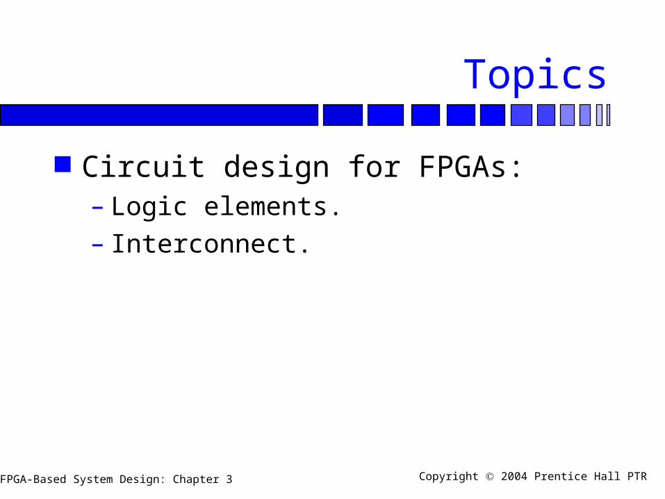
Topics
Circuit design for FPGAs:– Logic elements.– Interconnect.
FPGA-Based System Design: Chapter 3 Copyright 2004 Prentice Hall PTR
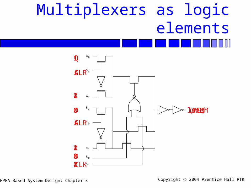
Multiplexers as logic elements
1
1
0
A
A
1B0
(AB)’
1
0
0
A
A
1B0
A^B
Q
0
D
CLR
CLR
00CLK
latch
FPGA-Based System Design: Chapter 3 Copyright 2004 Prentice Hall PTR
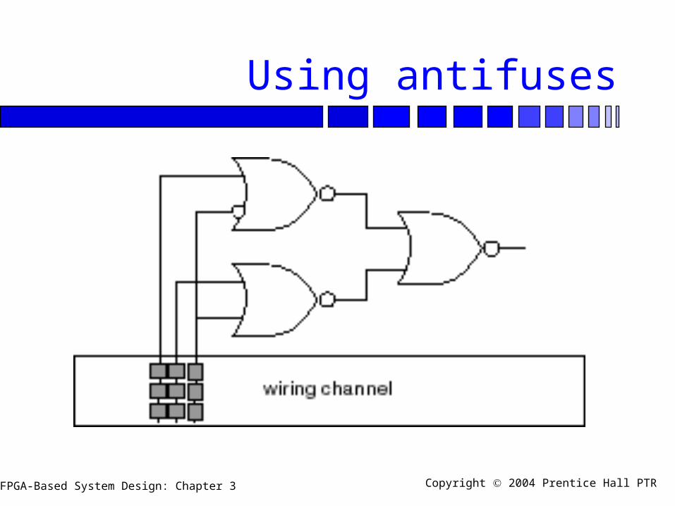
Using antifuses
FPGA-Based System Design: Chapter 3 Copyright 2004 Prentice Hall PTR
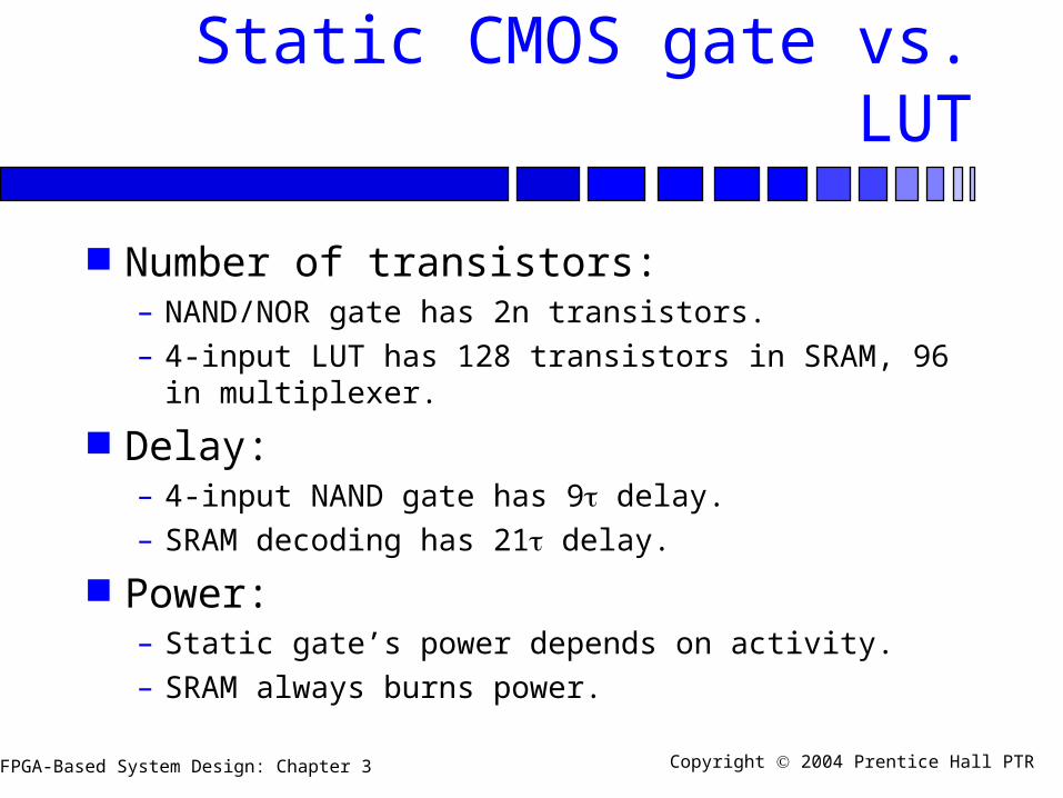
Static CMOS gate vs. LUT
Number of transistors:– NAND/NOR gate has 2n transistors.
– 4-input LUT has 128 transistors in SRAM, 96 in multiplexer.
Delay:– 4-input NAND gate has 9 delay.
– SRAM decoding has 21 delay.
Power:– Static gate’s power depends on activity.
– SRAM always burns power.
FPGA-Based System Design: Chapter 3 Copyright 2004 Prentice Hall PTR
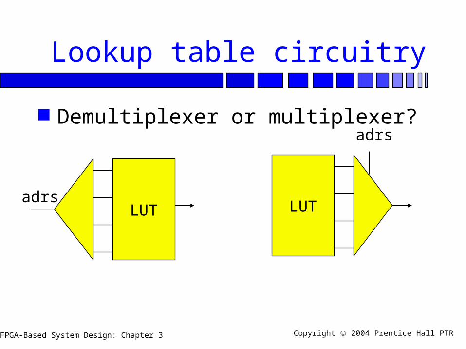
Lookup table circuitry
Demultiplexer or multiplexer?
LUTadrs
LUT
adrs
FPGA-Based System Design: Chapter 3 Copyright 2004 Prentice Hall PTR
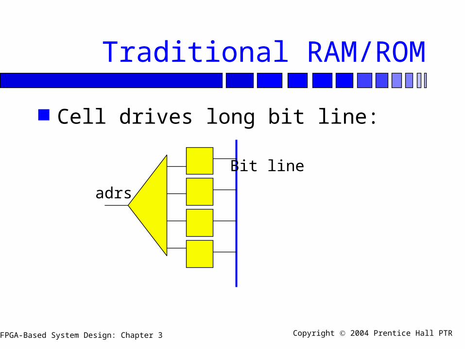
Traditional RAM/ROM
Cell drives long bit line:
Bit line
adrs
FPGA-Based System Design: Chapter 3 Copyright 2004 Prentice Hall PTR
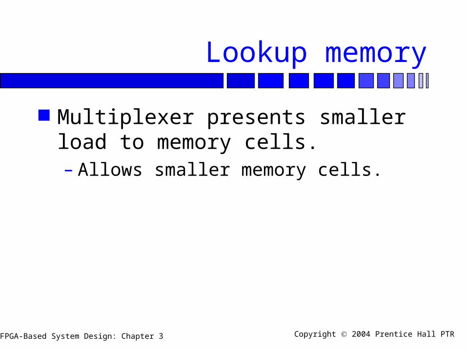
Lookup memory
Multiplexer presents smaller load to memory cells.– Allows smaller memory cells.
FPGA-Based System Design: Chapter 3 Copyright 2004 Prentice Hall PTR
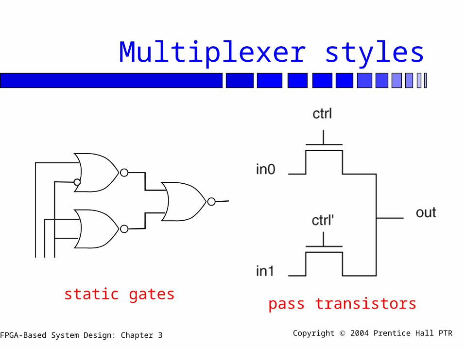
Multiplexer styles
static gatespass transistors
FPGA-Based System Design: Chapter 3 Copyright 2004 Prentice Hall PTR
Multiplexer design
Pass transistor multiplexer uses fewer transistors than fully complementary gates.
Pass transistor is somewhat faster than complementary switch:– Equal-strength p-type is 2.5X n-type width.
– Total resistance is 0.5X, total capacitance is 3.5X.
– RC delay is 0.5 x 3.5 = 1.75 times n-type switch.
FPGA-Based System Design: Chapter 3 Copyright 2004 Prentice Hall PTR
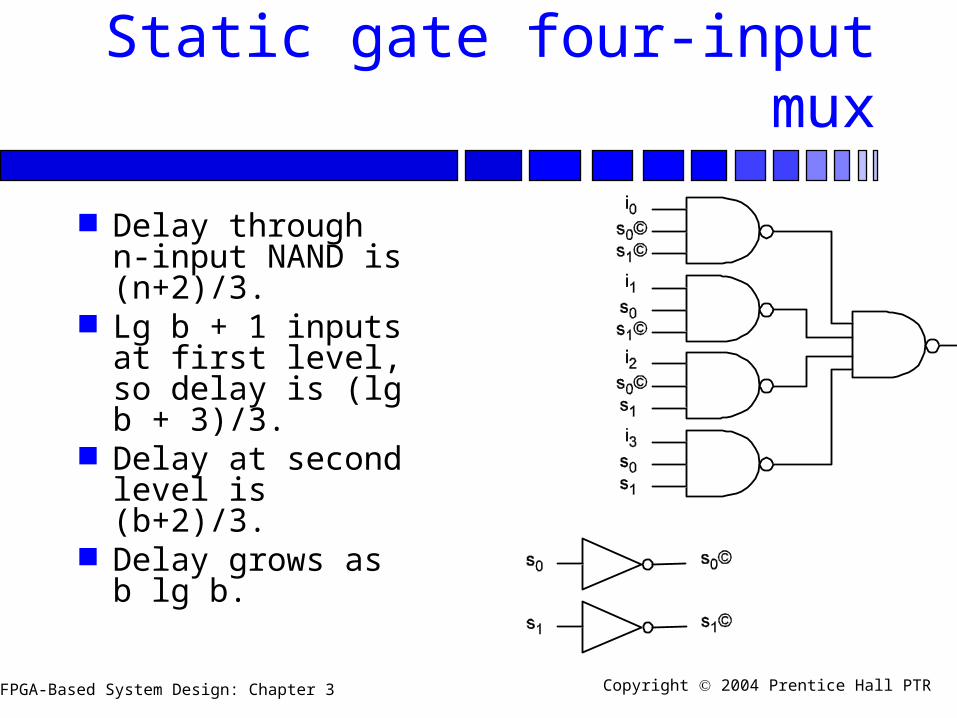
Static gate four-input mux
Delay through n-input NAND is (n+2)/3.
Lg b + 1 inputs at first level, so delay is (lg b + 3)/3.
Delay at second level is (b+2)/3.
Delay grows as b lg b.
FPGA-Based System Design: Chapter 3 Copyright 2004 Prentice Hall PTR
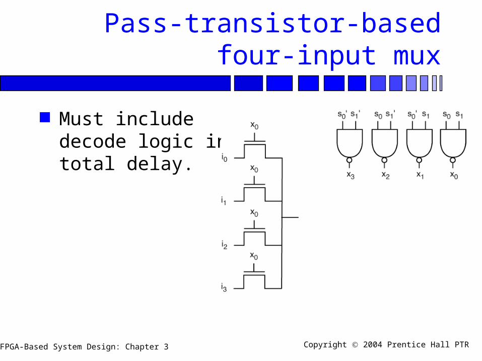
Pass-transistor-based four-input mux
Must include decode logic in total delay.
FPGA-Based System Design: Chapter 3 Copyright 2004 Prentice Hall PTR
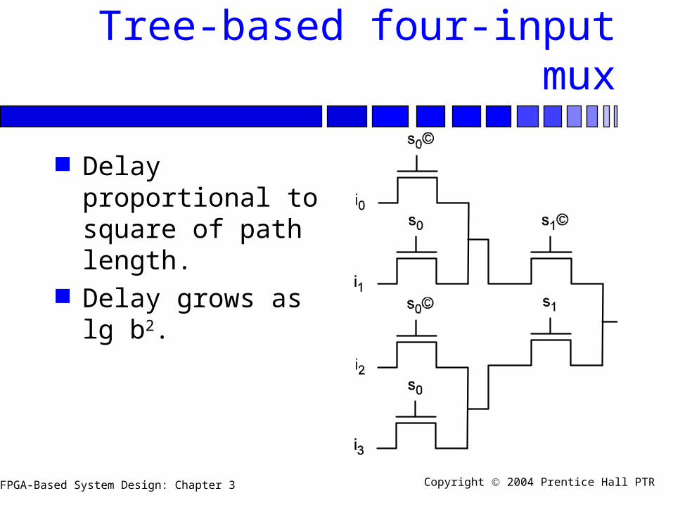
Tree-based four-input mux
Delay proportional to square of path length.
Delay grows as lg b2.
FPGA-Based System Design: Chapter 3 Copyright 2004 Prentice Hall PTR
LE output drivers
Must drive load:– Wire;– Destination LE.
Different types of wiring present different loads.
FPGA-Based System Design: Chapter 3 Copyright 2004 Prentice Hall PTR
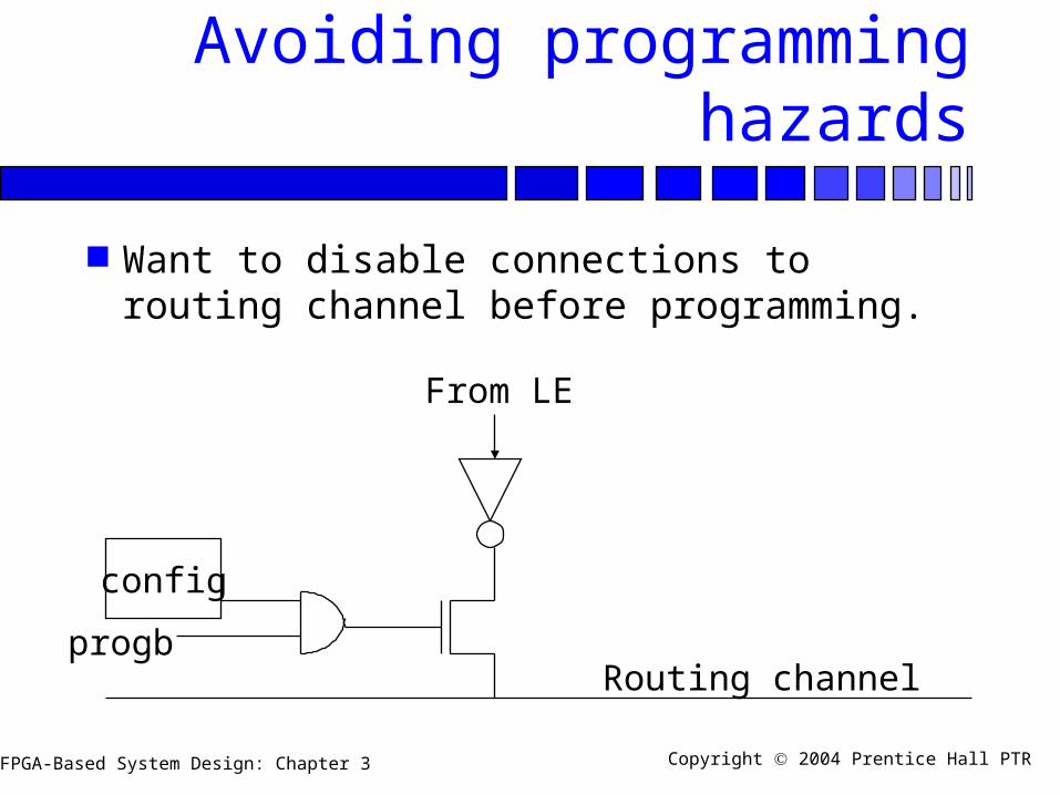
Avoiding programming hazards
Want to disable connections to routing channel before programming.
From LE
Routing channel
config
progb
FPGA-Based System Design: Chapter 3 Copyright 2004 Prentice Hall PTR
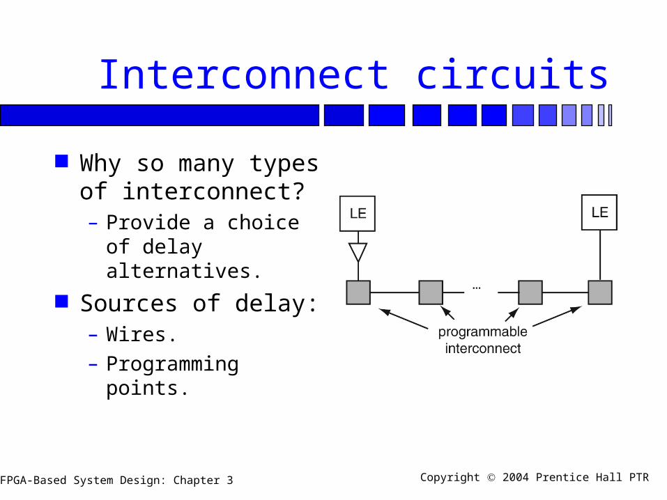
Interconnect circuits
Why so many types of interconnect?– Provide a choice of
delay alternatives.
Sources of delay:– Wires.
– Programming points.

FPGA-Based System Design: Chapter 3 Copyright 2004 Prentice Hall PTR
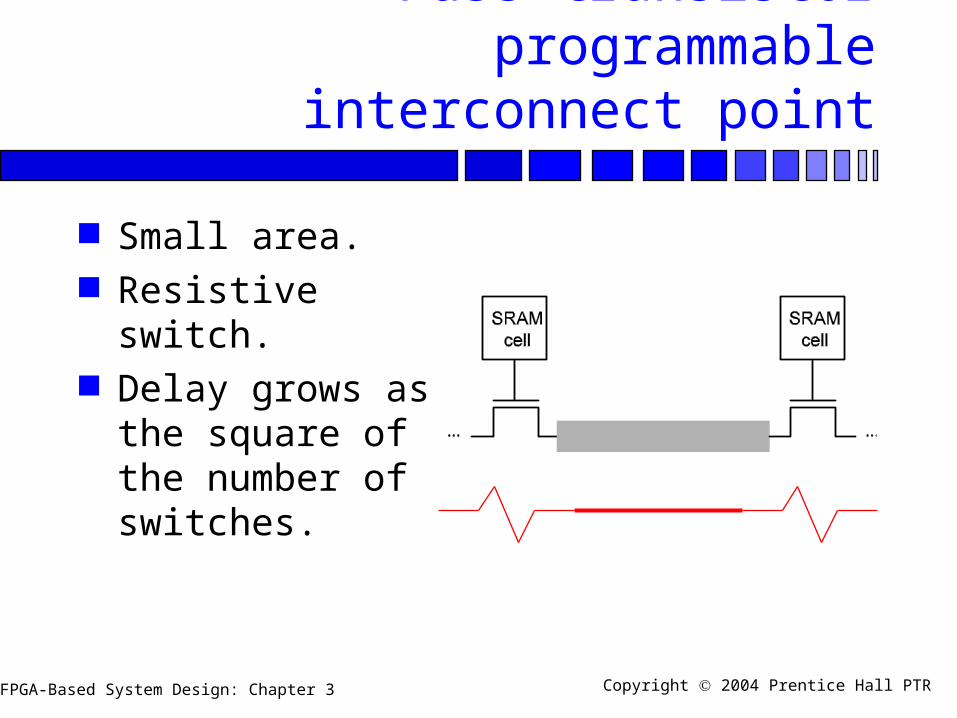
Styles of programmable interconnection point
pass transistor Three-state
FPGA-Based System Design: Chapter 3 Copyright 2004 Prentice Hall PTR
Pass transistor programmable interconnect point
Small area. Resistive switch. Delay grows as the
square of the number of switches.
FPGA-Based System Design: Chapter 3 Copyright 2004 Prentice Hall PTR
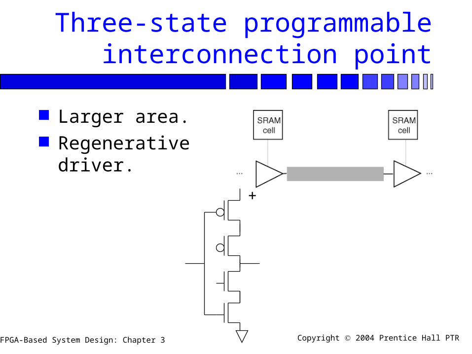
Three-state programmable interconnection point
Larger area. Regenerative driver.
+
FPGA-Based System Design: Chapter 3 Copyright 2004 Prentice Hall PTR
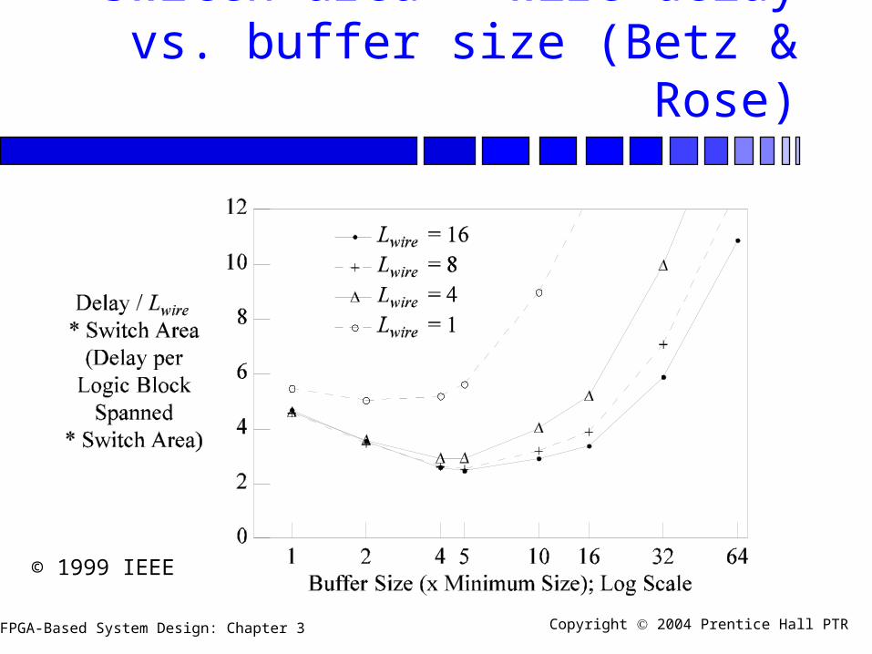
Switch area * wire delay vs. buffer size (Betz & Rose)
© 1999 IEEE
FPGA-Based System Design: Chapter 3 Copyright 2004 Prentice Hall PTR
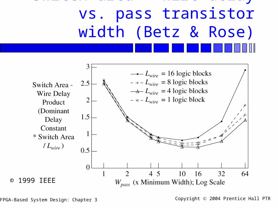
Switch area * wire delay vs. pass transistor width (Betz & Rose)
© 1999 IEEE
FPGA-Based System Design: Chapter 3 Copyright 2004 Prentice Hall PTR
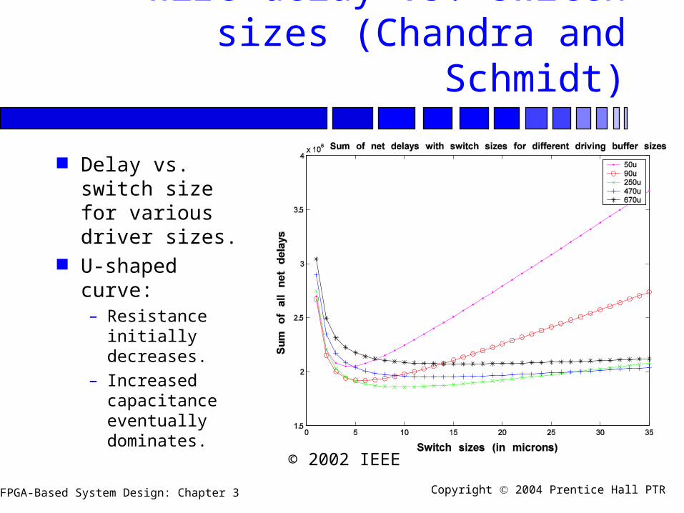
Wire delay vs. switch sizes (Chandra and Schmidt)
Delay vs. switch size for various driver sizes.
U-shaped curve:– Resistance
initially decreases.
– Increased capacitance eventually dominates.
© 2002 IEEE
FPGA-Based System Design: Chapter 3 Copyright 2004 Prentice Hall PTR
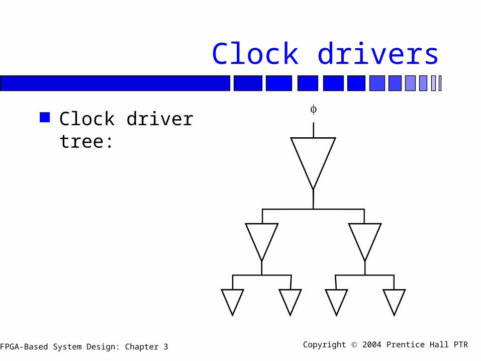
Clock drivers
Clock driver tree:
FPGA-Based System Design: Chapter 3 Copyright 2004 Prentice Hall PTR
Clock nets
Must drive all LEs. Design parameters:
– number of fanouts;– load per fanout;– wiring tree capacitance.
Determine optimal buffer sizes.
FPGA-Based System Design: Chapter 3 Copyright 2004 Prentice Hall PTR
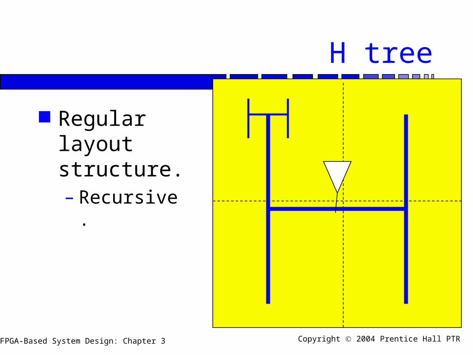
H tree
Regular layout structure.– Recursive.