Embed Size (px)
Citation preview

12
Electrica 2019; 19(1): 12-21
RESEARCH ARTICLE
FPGA Based Low Cost Automatic Test Equipment for Digital CircuitsAlp Arslan Bayrakci Department of Computer Engineering, Gebze Technical University, Kocaeli, Turkey
Corresponding Author: Alp Arslan Bayrakci
E-mail: [email protected]
Received: 30.04.2018
Accepted: 30.07.2018
© Copyright 2019 by Electrica Available online at http://electrica.istanbul.edu.tr
DOI: 10.26650/electrica.2018.28093
Cite this article as: Bayrakci AA. FPGA Based Low Cost Automatic Test Equipment for Digital Circuits. Electrica, 2019; 19(1): 12-21.
ABSTRACT
Testing of digital circuits is a crucial problem. There are two types of Automatic Test Equipment (ATE): Very precise but complex and expensive test equipments called high-end ATE and their approximate but cheap alternatives called low-end ATE. In this paper we propose a very cheap, FPGA based embedded low-cost ATE (ELATE) that is capable of functional, speed/delay and power consumption tests. It is composed of FPGA hardware with six FSM modules written in Verilog and a computer software (user interface) communicating with the FPGA through UART. It can handle different I/O combinations and can detect delay with 4ns precision. It can both visually show the resultant voltage/current-time graphs and store them as text files. The ATE is tested on different Design Under Test (DUT) devices like 8-bit and 12-bit adders and a square root circuit implemented on FPGA.Keywords: FPGA, automatic test equipment, digital circuit, functional, delay, power, test
Introduction
Importance of digital circuit testing increases while the complexity and difficulty to test also increase. There are different approaches in the literature for testing of digital circuits. Tests of ASICs with hundreds of input output pins and speeds at GHz rates are really complex and difficult. On the other hand many types of digital circuit prototypes need to be tested much before manufacturing phase.
This necessitates two types of automatic test equipments (ATE): high-end and low-end. High-end ATE is powerful, fast but expensive and complex. Big companies such as Advantest [1] and Teradyne [2] construct such fast and complex ATE with multi million dollars of cost in order to test many manufactured ASICs in a small amount of time and for many input test vectors. However, they are difficult to learn and too costly to be used by many digital circuit designers.
On the other hand, low-end ATE is relatively cheap and easier to use. There are different com-panies like Teseda [3], which try to lower the ATE cost [4]. Recently, due to the improvements at the FPGA technology, ATE based on FPGAs are popular in the literature [5, 6, 7]. They either can only handle functional tests or require reconfigurability to be adapted to different test circuits.
In this paper, we devise an ATE, capable of performing functional, speed and power tests with-out the need for reconfiguration, adaptively detecting when to stop the tests and consuming a reasonable amount of space. It was first introduced in [8] roughly. In this paper, we not only present the technical implementation of ATE using software and FSMs missing in [8] but also perform more tests on different arithmetic circuits implemented on FPGA. Also the use of sat-isfiability (SAT) is suggested to support functional tests.
Section 2 proposes the use of satisfiability for functional test expected output computation. Section 3 explains the implemented ATE software and Section 4 gives the technical implemen-tation of ATE hardware module by module to enable researchers implement their own ATE. Last section presents the results.
CER R A H PAŞA
İSTANBUL UNIVERSITYC E R R A H P A Ş A
13
Electrica 2019; 19(1): 12-21Bayrakci A.A. FPGA Based Low Cost Automatic Test Equipment for Digital Circuits
Satisfiability for Functional Tests
Satisfiability can be used to detect the output of the circuit when a particular input is given as well as detecting true paths in the circuit.
The circuit description can be converted into a conjunctive normal form (CNF) formula. Each logic gate has its own CNF convertion shown in as shown in Table 1 [9]. After converting each logic gate in the circuit into the equivalent CNF form and ANDing these CNFs into one CNF representing the whole cir-cuit, the input test vector for which the corresponding output is required, must be inserted into this circuit CNF.
The resultant circuit CNF can be used to detect the expected output when the primary inputs are inserted into the CNF cir-cuit description. For that purpose, the primary input signals with logic-1 should be directly inserted to CNF whereas for oth-ers (with logic-0) the complements of the primary input signals must be inserted into the circuit CNF. The resultant CNF formu-la can be given to a sat-solver [10]. As a result, all logic values for all nodes inside the circuit as well as the primary outputs can be extracted from the sat-solver result. The primary output val-ues gathered from this result are the expected outputs for the corresponding input vector, which can be used in functional tests as expected outputs that will be clarified later.
ATE Software
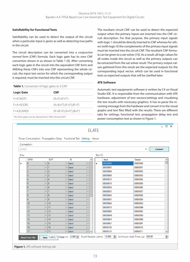
Automatic test equipments software is written by C# on Visual Studio IDE. It is responsible from the communication with ATE hardware, adjustment of test vectors/settings and visualizing the test results with necessary graphics. It has to parse the in-coming message from the hardware and convert it to the visual graphs and text files filled with the results. There are different tabs for settings, functional test, propagation delay test and power consumption test as shown in Figure 1.
Table 1. Conversion of logic gates to 3-CNF
Logic Gate CNF
F=A’ (NOT) (A+F).(A’+F’)
F=A+B (OR) (A+B+F’).(A’+F).(B’+F)
F=A.B (AND) (A’+B’+F).(A+F’).(B+F’)
*All other gates can be derived from AND, OR and NOT
Figure 1. ATE software Settings tab

14
Electrica 2019; 19(1): 12-21Bayrakci A.A. FPGA Based Low Cost Automatic Test Equipment for Digital Circuits
Settings tab includes four panes as shown in Figure 1. Top pane is for selecting the UART communication port with the ATE hard-ware. Left pane is for setting the input/output pin configurations. Right pane is for entering the input test vectors and the expected output vectors. Bottom pane is for entering the minimum wait time, supply voltage and shunt resistor values. All these settings can be saved as text file or they can be imported from a text file as shown in Figure 2. All vectors are given in hex format. This text file can be generated automatically by an automatic test pattern generation algorithm similar to the one devised in Section 2.1.
Functional test tab explained in Section 5.1 has a start test but-ton for starting the functional test with the vectors shown in Settings tab. Each output test vector is taken from ATE hard-ware through UART communication and shown at the func-tional test tab until all test vectors are over. If the resultant actu-al output vector is different than the expected one it is shown with red filled cell otherwise it is shown with green filled cell.
Propagation delay tab explained in Section 5.2 has two but-tons, one for starting the tests and other for saving the results to text file. There is also a graphics pane to show output signals corresponding to an input vector.
Power consumption tab is very similar to the propagation de-lay tab except the graph shows time vs. supply current data instead of output voltages. The resultant graphs can also be stored as jpeg or png images.
ATE Hardware
Proposed ATE has six main modules each of which is designed as finite state machine (FSM) in Verilog HDL and with Quartus II v16.1 software of Altera.
UART module
UART module consists of an eight state FSM for receiving data from the ATE software and a three state FSM for transmitting data to the ATE software. It is responsible not only to receive all user settings and the input test vectors but also to send back all test results to the ATE software. It is basically the slightly mod-ified version of the module in [11]. The UART communication is handled through a USB cable using virtual COM port drivers at the computer side. Different BAUD rates can be adjusted by setting parameters inside the module.
SPI module
This is a four state FSM module, which is only used to communi-cate with the analog to digital converter (ADC). It implements the SPI communication protocol and reads the resultant 12 bit digital output of the ADC chip whenever a measurement is required.
Test control module
This is one of the most important modules of ATE hardware. Having an eight state FSM, it is responsible to perform the pin
Figure 2. Text file to import user settings Figure 3. First four stages of Test Control Module

15
Electrica 2019; 19(1): 12-21Bayrakci A.A. FPGA Based Low Cost Automatic Test Equipment for Digital Circuits
input/output settings according to the user inputs, store input test vectors in its internal memory, start and manage all tests. Figure 3 shows the first four states while Figure 4 shows the second four states of the module.
STATE_WAIT_UART is the idle state waiting for incoming data from UART module. When a byte of data comes it checks whether it is zero. If it is zero, it transits into STATE_PIN_INIT state, where it adjusts each GPIO pin either as input or output
pin or not used. All GPIO pin settings are resolved at this state and by using the circuit shown in Figure 5.
In Figure 5 red output_select[31:0] signal and brown input_se-lect[35:0] signal are determined according to the pin setttings coming from UART. These two signals adjusts a GPIO pin using the multiplexers shown by two column of rectangles in the figure. Left hand side multiplexor input signals are 36 GPIO pins whereas the input signals of right hand side multiplexors are 32 bits inputs. This circuit enables to adjust any GPIO pin of the ATE hardware as input to DUT or as output from DUT, which resolves the issue of compatibility to any test circuit with any input/output pin config-uration provided that the total number of pins is bounded by 36.
This solution is better than reconfiguring the ATE hardware (FPGA) each time the DUT is changed as devised in [5].
After the multiplexor select signals are adjusted according to the current DUT by STATE_PIN_INIT state and with the first in-coming byte the state changes to STATE_TEST_FIRST where two bytes incoming from UART are combined and parsed in order to understand the test type (functional, delay or power). After the test type is determined in order to receive input test vectors the next state is STATE_TEST_READ_INPUT. FSM stays at this state until all input test vectors are stored inside the inter-nal memory of Test Control Module.
Last four states shown in Figure 4 are used for testing the DUT with each input test vector. The next two states (…TEST_START and …_SIGNAL_1) are responsible from sending the next stored input test vector to the corresponding test module. Then, STATE_TEST_SIGNAL_2 sends the start signal to the same module. This start signal activates the corresponding module that is responsible for finalizing the test and sending all results back to ATE software via UART module. STATE_WAIT_READY state waits until the testing for the corresponding test vector finishes and all results are sent back. After all tasks correspond-ing to the current input test vector finishes, the next test is ini-tiated until all input test vectors are utilized and test is over.
Figure 4. Second four stages of Test Control Module Figure 5. Pin Adjustment circuit in Test Control Module

16
Electrica 2019; 19(1): 12-21Bayrakci A.A. FPGA Based Low Cost Automatic Test Equipment for Digital Circuits
Functional test module
This module has four states as shown in Figure 6. It waits at STATE_IDLE until a start signal comes from Test Control Module. Start signal initiates the test by transisiton to STATE_START_TEST state, where it connects the current test vector coming from Test Control Module to the DUT inputs. Then it changes into STATE_WAIT state where it stays until the outputs are sta-bilized.
This part is crucial in order to ignore glitches at any of the out-puts. At this state, it waits a user given amount of time, which is specified through ATE software Settings Tab. During that time period if any of the outputs changes the timer is reset to zero. As a result, this state can only be exited when none of the outputs changes during the user specified minimum wait time. This guarantees that the outputs are stabilized. Re-sultant stable DUT outputs are recorded and the state changes to STATE_UART_SEND where the resultant DUT output is sent back to ATE software through UART Module. Then for the next input test vector, the iteration restarts from STATE_IDLE until all test iterations are over.
Here there is another critical choice of sending all data corre-sponding to a test vector back to ATE software before starting next test. This method results in much lower memory utiliza-tion than storing all data corresponding to all test vectors.
Propagation delay test module
This module has four states. It is very similar to the functional test module except it traces the time information and also re-cords the time instant at which an alteration occurs at one of the outputs. It checks the output signals 250,000,000 times in one second, i.e. with 4 nanoseconds intervals, which means that it cannot precisely detect delays for circuits faster than 250MHz.
The main problem of this method is that recording the output signals 250 million times in one second require a huge amount of space. Nonetheless, output alterations must be recorded in order to visually see the voltage vs. time plots of all output signals. We avoid this issue by just recording the times that an output signal changes inside the memory module. By this way, instead of 250 million records, the number of records are limit-ed by the number of output alterations. Allowing about 32000 alterations, a 256KB memory is practically enough. Second pre-caution is that all data corresponding to an input test vector is sent back to ATE software before starting the new test with the next input test vector.
Power consumption test module
This module has four states similar to the functional test mod-ule. It stays at STATE_IDLE until a start signal comes. Then it transits into STATE_ADC_READ, where it starts the analog to digital conversion of the voltage over the the shunt resistor connected to the circuit as in Figure 7. The voltage values are read via SPI Module at this state.
Figure 6. Functional Test Module FSM
Figure 7. Connection of shunt resistor for power tests
17
Electrica 2019; 19(1): 12-21Bayrakci A.A. FPGA Based Low Cost Automatic Test Equipment for Digital Circuits
At this point, it is important to know when to stop the ADC readings. In our solution, the reading of the analog voltage val-ues continues until the values return back to the values at the idle state, which means that the dynamic power consumption due to the given input test vector is over.
The last state named as STATE_UART_SEND sends all recorded data of the current input test vector back to the ATE software through UART module as it is done in delay test. Then the FSM returns back to the initial state, i.e. STATE_IDLE in order to start the test for the next input test vector coming from Test Control Module.
Again the strategy to send back all data of the current test vec-tor before switching to the next test vector avoids the memory insufficiency. Another technique that helps that is to avoid any recording unless there is a significant change in the shunt resis-tor voltage values, which is used to compute the instantaneous current drawn from the supply, and plotted as current vs. time graph.
Figure 8. Integer square root implemented as FSM (root=sqrt (num)) Figure 9. 8-bit adder functional test result

18
Electrica 2019; 19(1): 12-21Bayrakci A.A. FPGA Based Low Cost Automatic Test Equipment for Digital Circuits
Results
The test circuits are implemented on Altera Cyclone V GX board of Terasic. Tests performed for 8-bit, 12-bit adders and a square root unit written in Verilog by Quartus II tool. All test vectors are generated by a C program and given as text file input to the ATE software.
The minimum wait time supplied by the user is determined adaptively by checking the functional test results and increas-ing the minimum wait time until all results match with the ex-pected ones.
We implemented a square root arithmetic circuit unit on Al-tera Cyclone V FPGA by writing the module with two state FSM as shown in Figure 8. It takes 20 bits of input and 12 bits of output as the integer square root of the input. The adders are written in behavioral Verilog using the classical ‘+’ opera-tor.
Functional test results
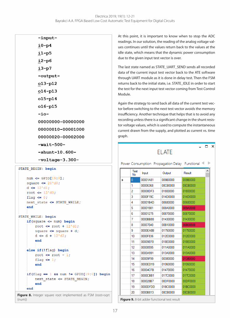
The results of functional test for 8-bit adder and square root units are shown by Figure 9 and 10 respectively. Only the first 20 test vectors are shown for demonstration purposes. The input col-umn shows the input vector, the output column shows the ex-pected output and the result column shows the actual result tak-en from DUT. Green represents that the DUT result is same as the expected output. As it is seen in both figures there are red entries which means that the result is different from the expected out-put. The red entries are made intentionally in order to show that the ATE works accurately. In other words, for the red entries, we intentionally write wrong numbers as expected output.
In Figure 9, the 6th input 00001275 means that the adder takes (12)16 and (75)16 as input numbers to be added and the result is (87)16, which is written as 00870000 as the two digits next to the most significant two digits represent the output of DUT. The 5th entry is red because the addition result is different than the expected output, which is intentionally written false.
Similarly in Figure 10, the 10th input is 00000064 means that the input number is (64)16 and the actual square root result is 10 which is shown as 0000000A. It is shown as red because we intentionally write (003)16 as the expected output to check the proposed ATE.
Figure 11. Propagation delay plot for input test vector (64)16Figure 10. Square root functional test result
19
Electrica 2019; 19(1): 12-21Bayrakci A.A. FPGA Based Low Cost Automatic Test Equipment for Digital Circuits
Functional tests with 1024 random samples for each of all three test circuits resulted accurately.
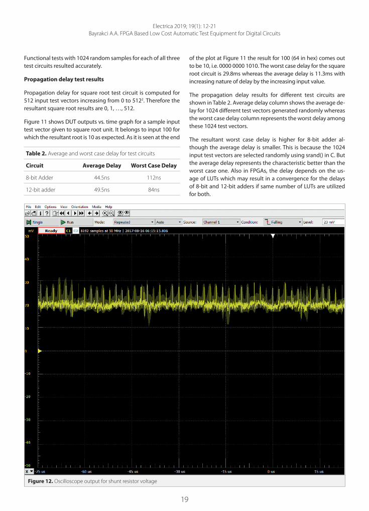
Propagation delay test results
Propagation delay for square root test circuit is computed for 512 input test vectors increasing from 0 to 5122. Therefore the resultant square root results are 0, 1, …, 512.
Figure 11 shows DUT outputs vs. time graph for a sample input test vector given to square root unit. It belongs to input 100 for which the resultant root is 10 as expected. As it is seen at the end
of the plot at Figure 11 the result for 100 (64 in hex) comes out to be 10, i.e. 0000 0000 1010. The worst case delay for the square root circuit is 29.8ms whereas the average delay is 11.3ms with increasing nature of delay by the increasing input value.
The propagation delay results for different test circuits are shown in Table 2. Average delay column shows the average de-lay for 1024 different test vectors generated randomly whereas the worst case delay column represents the worst delay among these 1024 test vectors.
The resultant worst case delay is higher for 8-bit adder al-though the average delay is smaller. This is because the 1024 input test vectors are selected randomly using srand() in C. But the average delay represents the characteristic better than the worst case one. Also in FPGAs, the delay depends on the us-age of LUTs which may result in a convergence for the delays of 8-bit and 12-bit adders if same number of LUTs are utilized for both.
Figure 12. Oscilloscope output for shunt resistor voltage
Table 2. Average and worst case delay for test circuits
Circuit Average Delay Worst Case Delay
8-bit Adder 44.5ns 112ns
12-bit adder 49.5ns 84ns

20
Electrica 2019; 19(1): 12-21Bayrakci A.A. FPGA Based Low Cost Automatic Test Equipment for Digital Circuits
Power consumption test results
Power consumption is the weakest part of our ATE. Because the sampling rate of the used ADC is as low as 500ksps, therefore the dynamic current fluctuations in nanosecond intervals can-not be captured by our ADC. However we tested the accuracy of our power consumption test by comparing with the Ana-log Discovery oscilloscope output where we only manage to measure the idle power consumption for the Stellaris Lauch-pad MCU development board of Texas Instruments. Figure 12 shows the Analog Discovery oscilloscope output for shunt re-sistor voltage for 100us interval and Figure 13 shows the resul-tant ATE shunt resistor current plot captured by ATE software for 300us interval. As the shunt resistor is about 11Ohm both plots give similar results which emprically verify the power con-sumption test result of ATE.
Conclusion
The proposed ATE performs very well in all functional tests. Al-though the final output voltage values are accurate for prop-agation delay voltage-time plots, further investigation and improvement are required in order to be sure about the actual delay. For that purpose precise tools to detect the actual de-
lay of the circuits can be employed. Power consumption tests are working but the sampling rate of ADC must be really very high in tens of GHz in order to detect dynamic supply current changes. However, ATE proposed in this paper constitutes a good start from scratch and this model can further be im-proved by inserting more expensive but precise hardware as well as hardware and software enhancements.
Peer-review: Externally peer-reviewed.
Conflict of Interest: The author has no conflicts of interest to declare.
Financial Disclosure: This work is supported by The Scientific and Technological Research Council of Turkey (TUBITAK) under Grant No. 116E296.
References
1. IC Test Systems – Advantest (March 2018).Available: https://www.advantest.com/products/ic-test-systems.
2. Production Board Test Teradyne (March 2018). Available: http://www.teradyne.com/products/production-board-test.
3. Teseda Corporation: Silicon Failure Analysis and Yield Enhance-ment (March 2018). Available: http://www.teseda.com.
4. Teseda breaks $200 per pin ATE barrier (March 2018). Available: http://www.eetimes.com/document.asp?doc_id=1175064.
5. L. Mostardini, L. Bacciarelli, L. Fanucci, L. Bertini, M. Tonarelli, M. De Marinis, “FPGA-based low-cost automatic test equipment for digi-tal integrated circuits”, IEEE International Workshop on Intelligent Data Acquisition and Advanced Computing Systems: Technology and Applications, Rende, pp. 32-37, 2009. [CrossRef ]
6. J. H. M. Escobar, J. SachBe, S. Ostendorff, H. D. Wuttke, “Automatic generation of an FPGA based embedded test system for printed circuit board testing”, 13th Latin American Test Workshop (LATW), Quito, Ecuador, pp. 1-6, 2012. [CrossRef ]
7. I. Aleksejev, A. Jutman, S. Devadze, S. Odintsov, T. Wenzel, “FP-GA-based synthetic instrumentation for board test,” IEEE Interna-tional Test Conference, Anaheim, CA, pp. 1-10, 2012. [CrossRef ]
8. A. A. Bayrakci, “ELATE: Embedded low cost automatic test equip-ment for FPGA based testing of digital circuits”, 2017 10th Inter-national Conference on Electrical and Electronics Engineering (ELECO), Bursa, 2017, pp. 1281-1285.
9. F. S. Marques, R. P. Ribas, S. Sapatnekar, and A. I. Reis. “A new ap-proach to the use of satisfiability in false path detection.” Proceed-ings of the 15th ACM Great Lakes symposium on VLSI (GLSVLSI ‘05). ACM, New York, NY, USA, pp 308-311, 2005. [CrossRef ]
10. N. Eén, N. Sörensson. “An extensible SAT-solver”, International con-ference on theory and applications of satisfiability testing. Spring-er, Berlin, Heidelberg, 2003.
11. Documented Verilog UART (March 2018). Available: https://open-cores.org/project/osdvu.
Figure 13. Square root circuit current-time graph

21
Electrica 2019; 19(1): 12-21Bayrakci A.A. FPGA Based Low Cost Automatic Test Equipment for Digital Circuits
Alp Arslan Bayrakçı received the B.S. degree in electrical and electronics engineering from Middle East Tech-nical University, Ankara, Turkey, in 2004, and the Ph.D. degree in computer engineering from Koç University, Istanbul, Turkey, in 2010. He has been with Gebze Technical University, Gebze, Turkey, since 2011. His current research interests include statistical timing analysis, hardware security, and computer-aided design method-ologies.


![Automatic Brain Tumor Segmentation Using FPGA Platform · transform edge detection algorithm using FPGA approach proposed by Selvathi and Dhara ni [15]. T he above background of current](https://img.pdfslide.us/doc/110x75/5e15d72bdcc4c4249636f163/automatic-brain-tumor-segmentation-using-fpga-platform-transform-edge-detection.jpg)