Embed Size (px)
Citation preview
ECE 435 Embedded SystemsSpring 2019
FPGA architecture and design technology
Nikos Bellas
Computer and Communications Engineering DepartmentUniversity of Thessaly
1CE435 - Embedded Systems
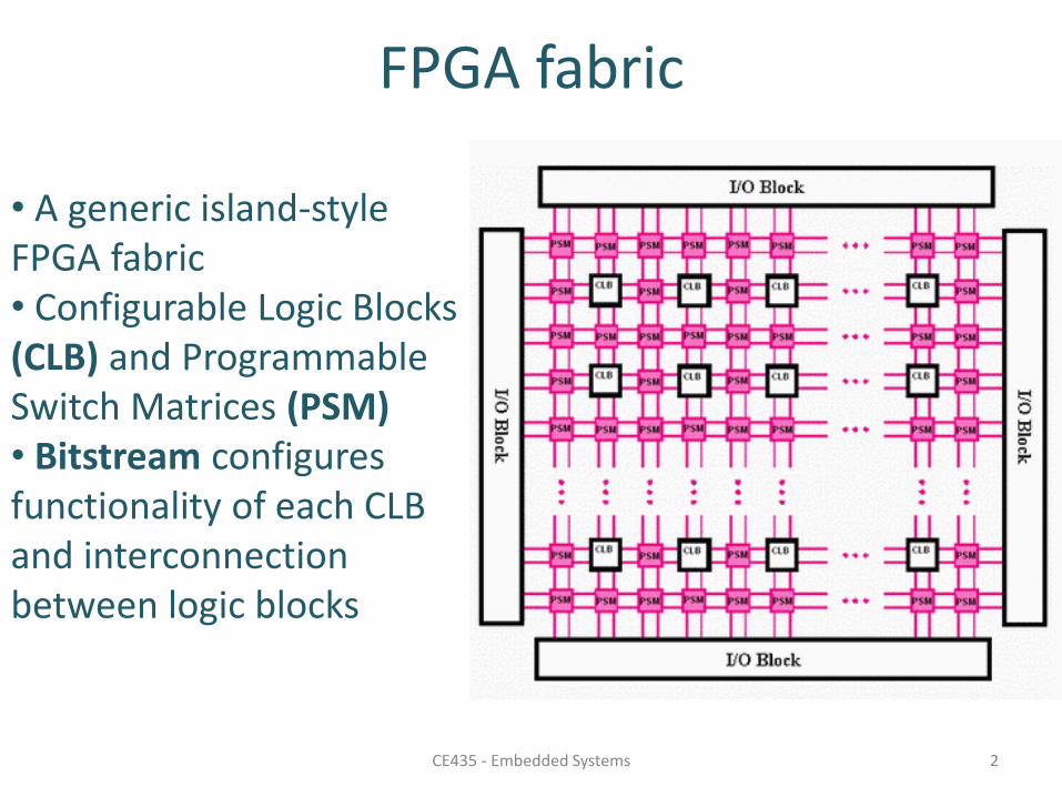
FPGA fabric
• A generic island-style FPGA fabric• Configurable Logic Blocks (CLB) and Programmable Switch Matrices (PSM)• Bitstream configures functionality of each CLB and interconnection between logic blocks
2CE435 - Embedded Systems
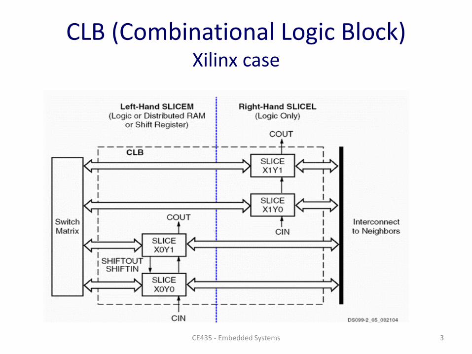
CLB (Combinational Logic Block)Xilinx case
CE435 - Embedded Systems 3
Basic Architecture 4
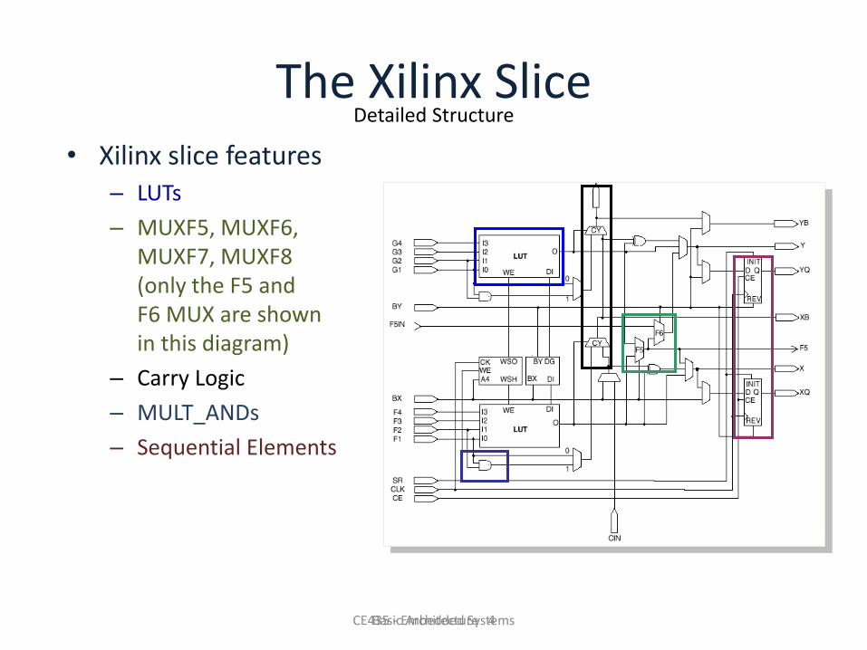
The Xilinx Slice
• Xilinx slice features– LUTs
– MUXF5, MUXF6, MUXF7, MUXF8 (only the F5 and F6 MUX are shown in this diagram)
– Carry Logic
– MULT_ANDs
– Sequential Elements
Detailed Structure
CE435 - Embedded Systems
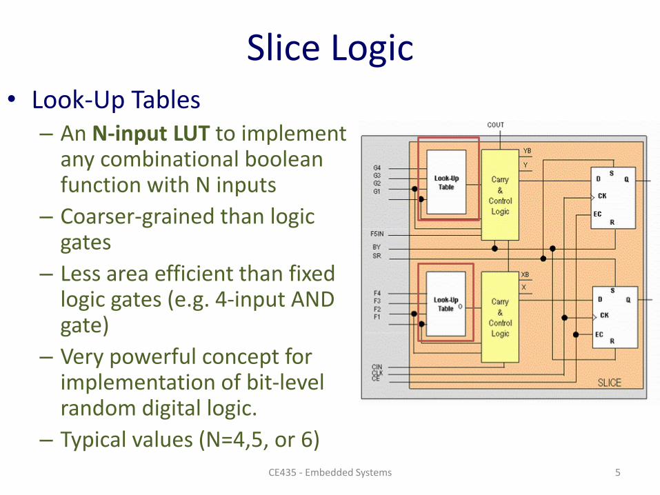
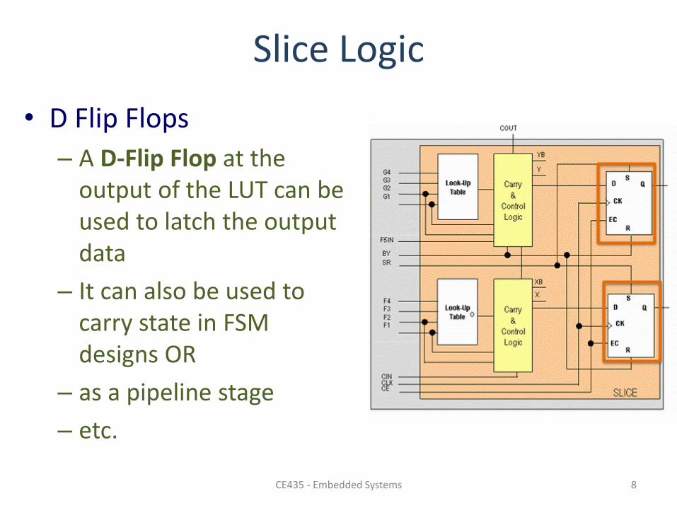
Slice Logic
CE435 - Embedded Systems 5
• Look-Up Tables– An N-input LUT to implement
any combinational boolean function with N inputs
– Coarser-grained than logic gates
– Less area efficient than fixed logic gates (e.g. 4-input AND gate)
– Very powerful concept for implementation of bit-level random digital logic.
– Typical values (N=4,5, or 6)
LUT
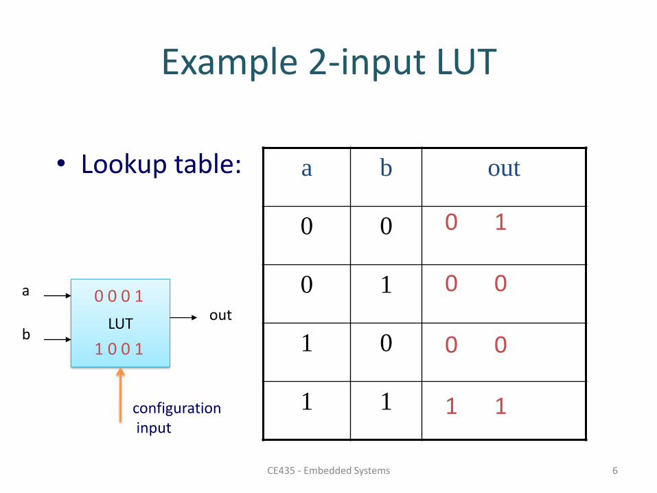
Example 2-input LUT
• Lookup table: a b out
0 0
0 1
1 0
1 1
a
bout
0
0
0
1
0 0 0 1
1
0
0
1
1 0 0 1
6CE435 - Embedded Systems
configurationinput
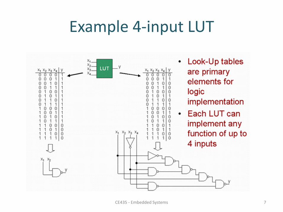
Example 4-input LUT
CE435 - Embedded Systems 7
Slice Logic
• D Flip Flops
– A D-Flip Flop at the output of the LUT can be used to latch the output data
– It can also be used to carry state in FSM designs OR
– as a pipeline stage
– etc.
8CE435 - Embedded Systems
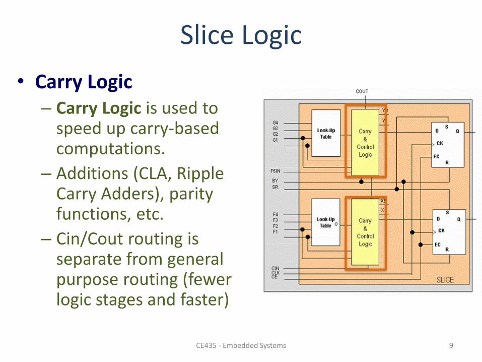
Slice Logic
• Carry Logic– Carry Logic is used to
speed up carry-based computations.
– Additions (CLA, Ripple Carry Adders), parity functions, etc.
– Cin/Cout routing is separate from general purpose routing (fewer logic stages and faster)
9CE435 - Embedded Systems
Basic Architecture 10
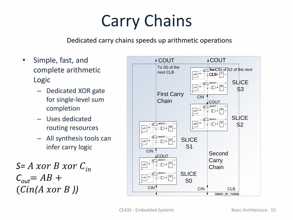
Carry Chains
• Simple, fast, and complete arithmetic Logic
– Dedicated XOR gate for single-level sum completion
– Uses dedicated routing resources
– All synthesis tools can infer carry logic
COUT COUT
SLICE
S0
SLICE
S1
Second
Carry
Chain
To S0 of the
next CLBTo CIN of S2 of the next
CLB
First Carry
Chain
SLICE
S3
SLICE
S2
COUT
COUT
CIN
CIN
CIN CIN CLB
Dedicated carry chains speeds up arithmetic operations
S= 𝐴 𝑥𝑜𝑟 𝐵 𝑥𝑜𝑟 𝐶𝑖𝑛Cout= 𝐴𝐵 +(𝐶𝑖𝑛(𝐴 𝑥𝑜𝑟 𝐵 ))
CE435 - Embedded Systems
Basic Architecture 11
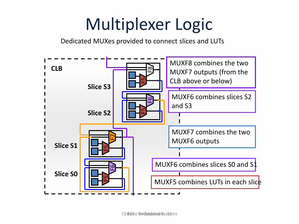
Multiplexer Logic
F5F8
F5F6
CLB
Slice S3
Slice S2
Slice S0
Slice S1
F5F7
F5F6
MUXF8 combines the two MUXF7 outputs (from the CLB above or below)
MUXF6 combines slices S2 and S3
MUXF7 combines the two MUXF6 outputs
MUXF6 combines slices S0 and S1
MUXF5 combines LUTs in each slice
Dedicated MUXes provided to connect slices and LUTs
CE435 - Embedded Systems
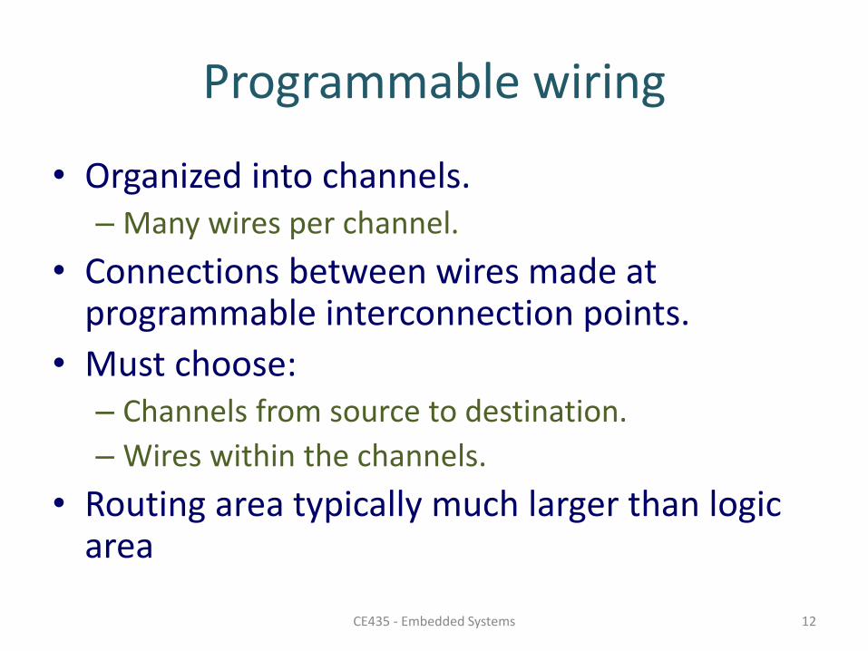
Programmable wiring
• Organized into channels.– Many wires per channel.
• Connections between wires made at programmable interconnection points.
• Must choose:– Channels from source to destination.
– Wires within the channels.
• Routing area typically much larger than logic area
12CE435 - Embedded Systems
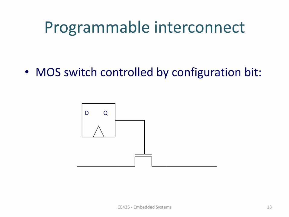
Programmable interconnect
• MOS switch controlled by configuration bit:
D Q
13CE435 - Embedded Systems
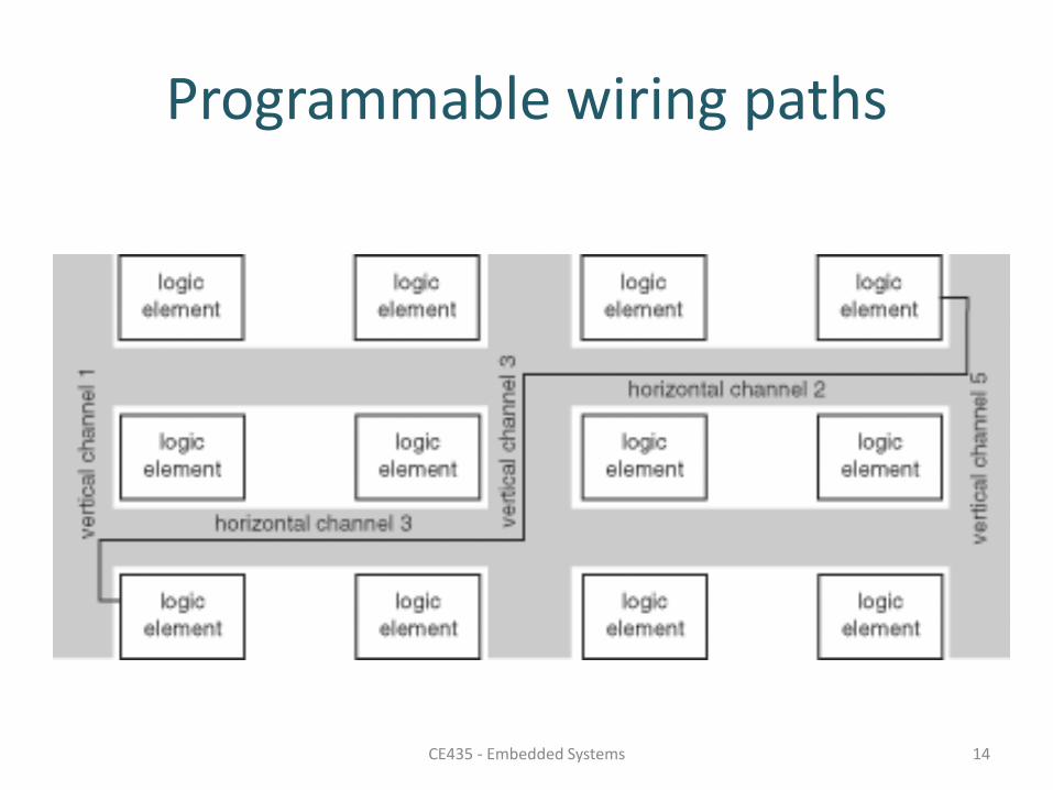
Programmable wiring paths
14CE435 - Embedded Systems
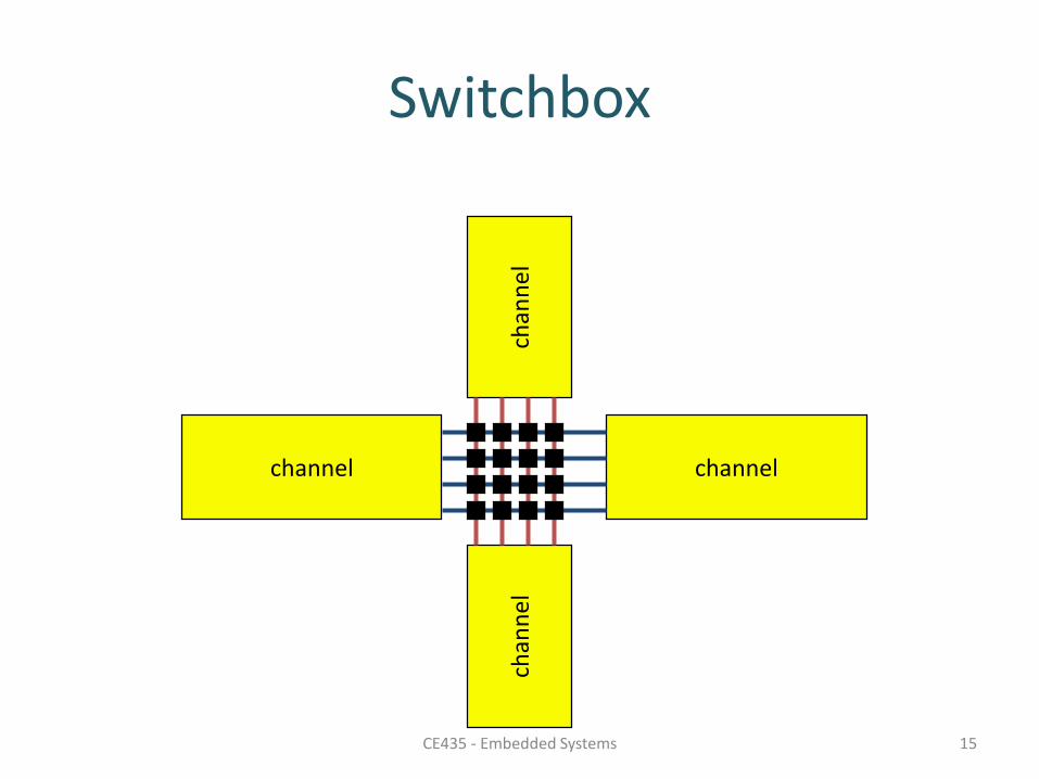
Switchbox
channel channel
chan
ne
lch
ann
el
15CE435 - Embedded Systems
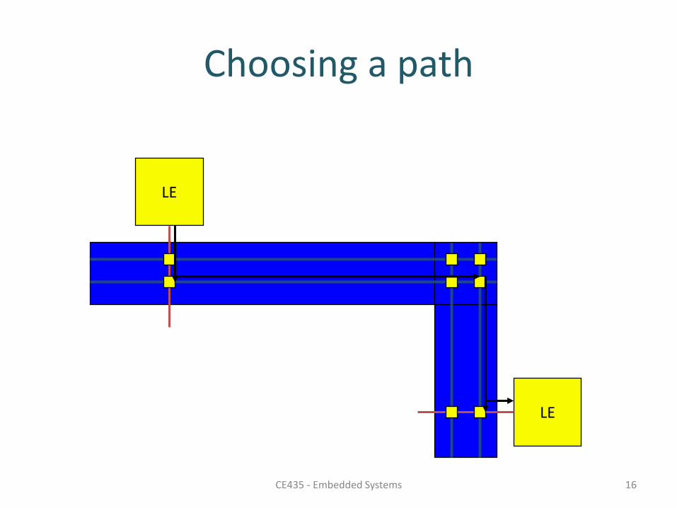
Choosing a path
LE
LE
16CE435 - Embedded Systems
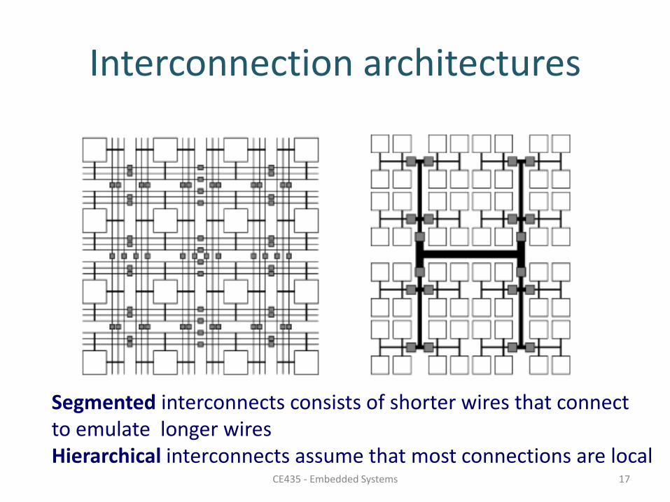
Interconnection architectures
CE435 - Embedded Systems 17
Segmented interconnects consists of shorter wires that connectto emulate longer wiresHierarchical interconnects assume that most connections are local
Routing problems
• Global routing:
– Which combination of channels?
• Local routing:
– Which wire in each channel?
• Routing metrics:
– Net length.
– Delay.
18CE435 - Embedded Systems
I/O
• Fundamental selection: input, output, three-state?
• Additional features:
– Register.
– Voltage levels.
– Slew rate.
19CE435 - Embedded Systems
Configuration
• Must set control bits for:
– LE.
– Interconnect.
– I/O blocks.
• Usually configured off-line.
– Separate burn-in step (antifuse).
– At power-up (SRAM).
20CE435 - Embedded Systems
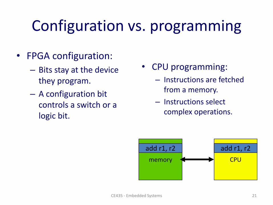
Configuration vs. programming
• FPGA configuration:
– Bits stay at the device they program.
– A configuration bit controls a switch or a logic bit.
• CPU programming:
– Instructions are fetched from a memory.
– Instructions select complex operations.
CPUmemory
add r1, r2 IRadd r1, r2
21CE435 - Embedded Systems
Reconfiguration
• Some FPGAs are designed for fast configuration.
– A few clock cycles, not thousands of clock cycles.
• Allows hardware to be changed on-the-fly.
22CE435 - Embedded Systems
FPGA fabric architecture questions
• Given limited area budget:
– How many logic elements?
– How much interconnect?
– How many I/O blocks?
23CE435 - Embedded Systems
Logic element questions
• How many inputs?
• How many functions?– All functions of n inputs or eliminate some
combinations?
– What inputs go to what pieces of the function?
• Any specialized logic?– Adder, etc.
• What register features?
24CE435 - Embedded Systems
Interconnect questions
• How many wires in each channel?
• Uniform distribution of wiring?
• How should wires be segmented?
• How rich is interconnect between channels?
• How long is the average wire?
• How much buffering do we add to wires?
25CE435 - Embedded Systems
I/O block questions
• How many pins?
– Maximum number of pins determined by package type.
• Are pins programmed individually or in groups?
• Can all pins perform all functions?
• How many logic families do we support?
26CE435 - Embedded Systems
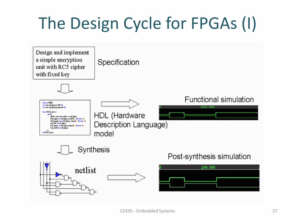
The Design Cycle for FPGAs (I)
CE435 - Embedded Systems 27
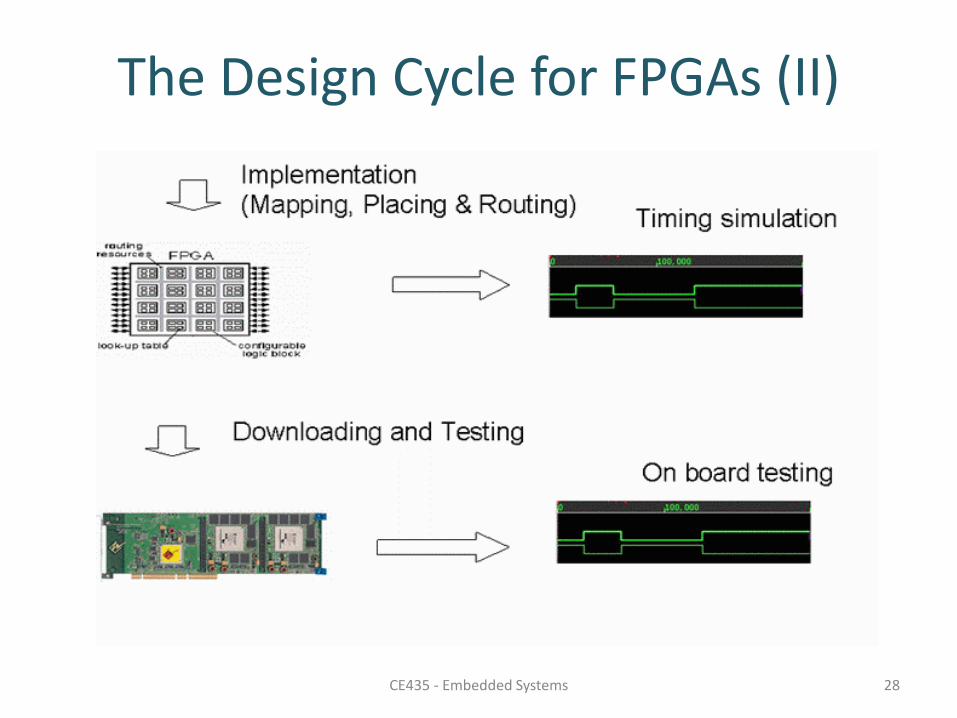
The Design Cycle for FPGAs (II)
CE435 - Embedded Systems 28
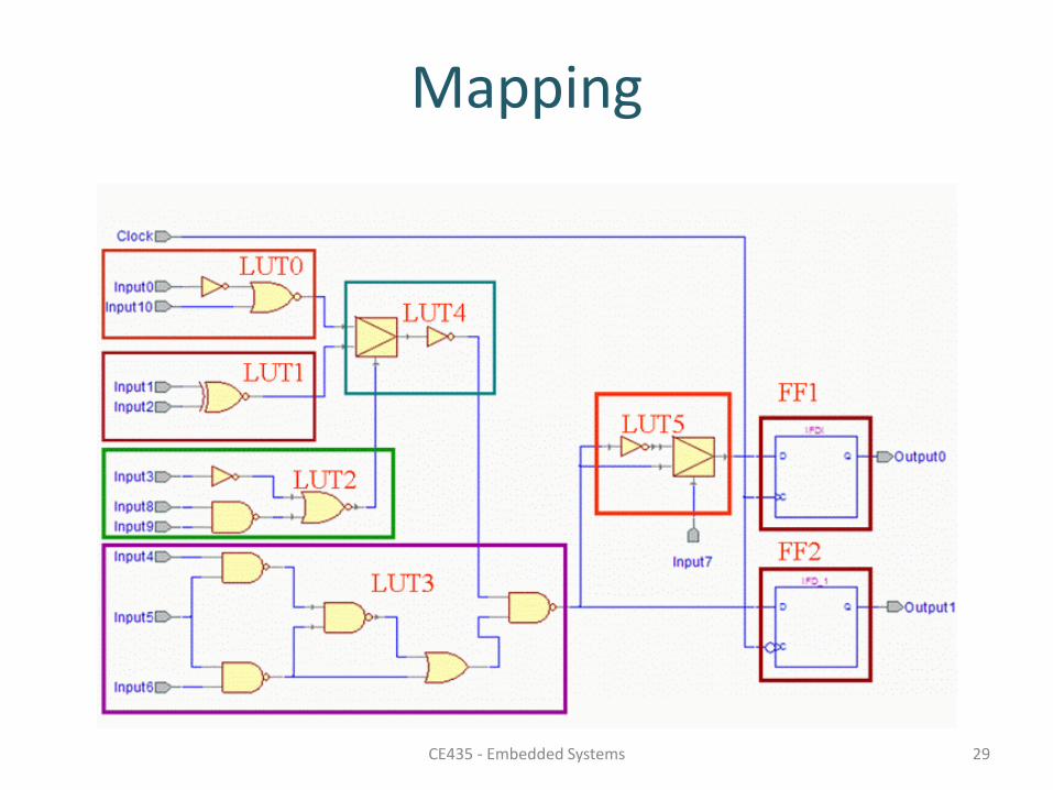
Mapping
CE435 - Embedded Systems 29
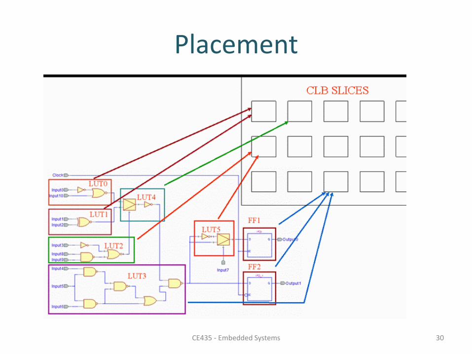
Placement
CE435 - Embedded Systems 30
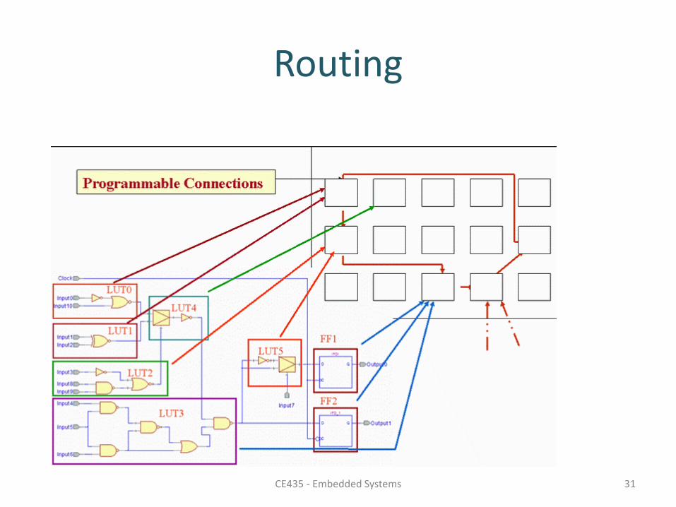
Routing
CE435 - Embedded Systems 31
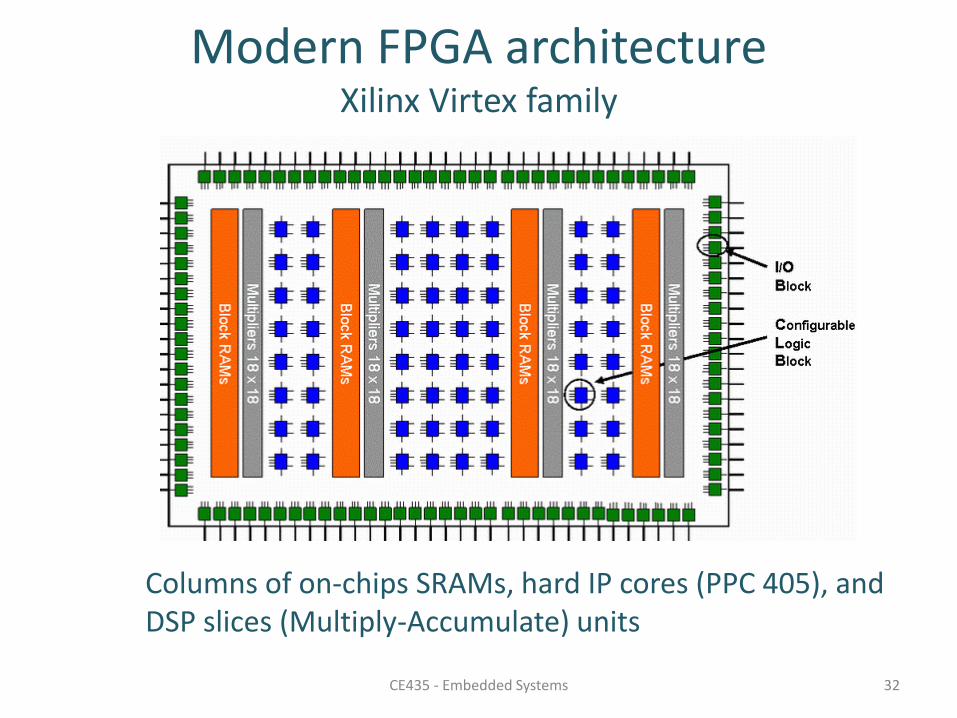
Modern FPGA architectureXilinx Virtex family
CE435 - Embedded Systems 32
Columns of on-chips SRAMs, hard IP cores (PPC 405), andDSP slices (Multiply-Accumulate) units
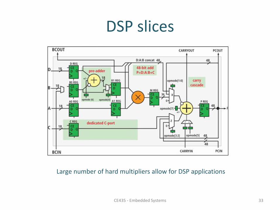
DSP slices
CE435 - Embedded Systems 33
Large number of hard multipliers allow for DSP applications
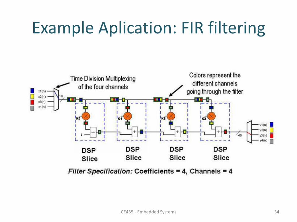
Example Aplication: FIR filtering
CE435 - Embedded Systems 34
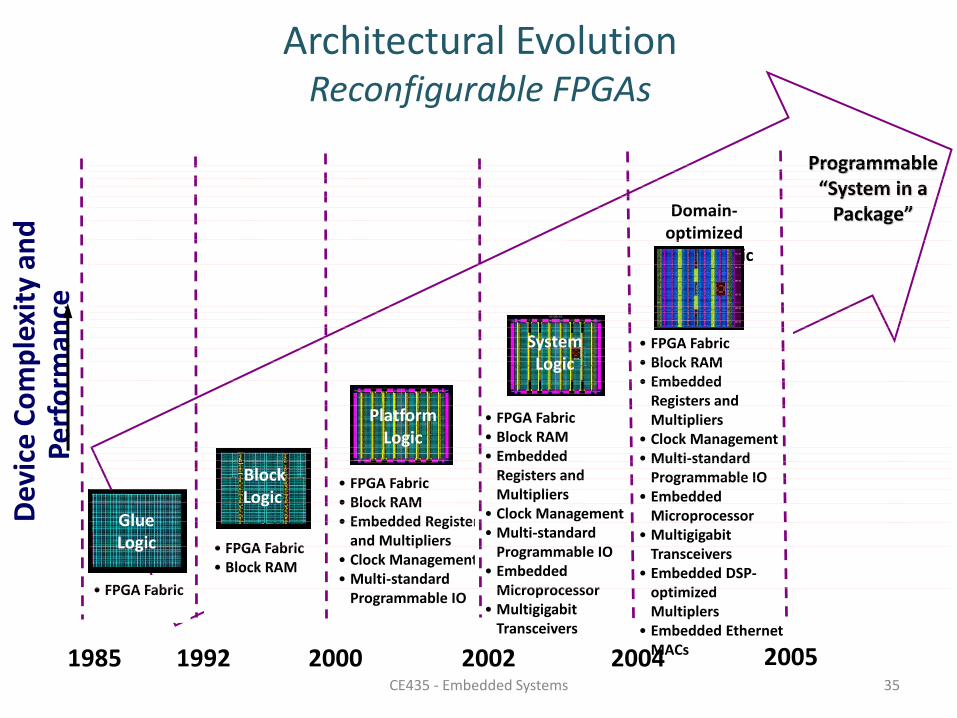
Architectural EvolutionReconfigurable FPGAs
Dev
ice
Co
mp
lexi
ty a
nd
P
erf
orm
ance
1985 1992 2000 2002 2004
• FPGA Fabric• Block RAM• Embedded Registers
and Multipliers• Clock Management• Multi-standard
Programmable IO
• FPGA Fabric• Block RAM
• FPGA Fabric
Domain-optimized
System Logic
• FPGA Fabric• Block RAM• Embedded
Registers and Multipliers
• Clock Management• Multi-standard
Programmable IO• Embedded
Microprocessor• Multigigabit
Transceivers
• FPGA Fabric• Block RAM• Embedded
Registers and Multipliers
• Clock Management• Multi-standard
Programmable IO• Embedded
Microprocessor• Multigigabit
Transceivers• Embedded DSP-
optimized Multiplers
• Embedded Ethernet MACs
GlueLogic
BlockLogic
PlatformLogic
SystemLogic
2005
Programmable “System in a
Package”
35CE435 - Embedded Systems