Embed Size (px)
Citation preview
FPGA-Accelerated Deserialization of Object Structures
Rene Mueller, Ken Eguro
Microsoft Research
September 2009
Technical Report
MSR-TR-2009-126
Microsoft Research
Microsoft Corporation
One Microsoft Way
Redmond, WA 98052
2
FPGA-Accelerated Deserialization of Object Structures
René Müller, Ken Eguro Microsoft Research
ABSTRACT
Emerging large scale multicore architectures provide abundant
resources for parallel computation. In practice, however, the
speedup gained by parallelization is limited by the fraction of
code that inherently needs to be executed sequentially (Amdahl’s
Law). An important example is object serialization and deseriali-
zation. As any other I/O operation, they are inherently sequential
and thus cannot immediately benefit from multicore technology.
In this work, we study acceleration by offloading this sequential
processing to a custom hardware circuit in an FPGA. The FPGA
is placed in the data path between the network interface and the
CPU.
First, we present an efficient FPGA implementation for C++
object deserialization which we compare with the traditional
approach. In the second part of the paper we describe how to
create FPGA circuits, i.e., VHDL/Verilog code for C++ object
structures based on the object layout and the serialization proce-
dure.
1. INTRODUCTION As future system architectures will consist of multiple cores the
problem the software community is confronted with is how to
efficiently make use of these additional resources. Most research
focus is devoted to parallel algorithms and cache-conscious im-
plementations. However, obtaining high speedups by just using
multicore architectures alone is difficult (Laurus 2009). In particu-
lar, the speedup that can be obtained is limited by the inherently
sequential fraction of a program. This is known as Amdahl’s Law
(Amdahl 1967). Its statement is the following: If by optimization
(multicore, etc.) the parallel fraction f of a program experiences a
speedup of S the speedup of the overall program is
Speedup =1
1 − 𝑓 +𝑓
𝑆 .
Clearly, for 𝑆 → ∞ the speedup is bound to 11 − 𝑓 by the se-
quential fraction 1 − 𝑓.
In practice, the sequential fraction of a program involves I/O
operations such as disk and network access, i.e., serialization of
data. In this work, one particular type of serialization and deseria-
lization is considered; object marshalling and unmarshalling in
Remote Procedure Calls (RPCs). RPCs play an important role in
modern distributed and networked systems. To that extent, mini-
mizing overhead and communication cost is crucial. Our approach
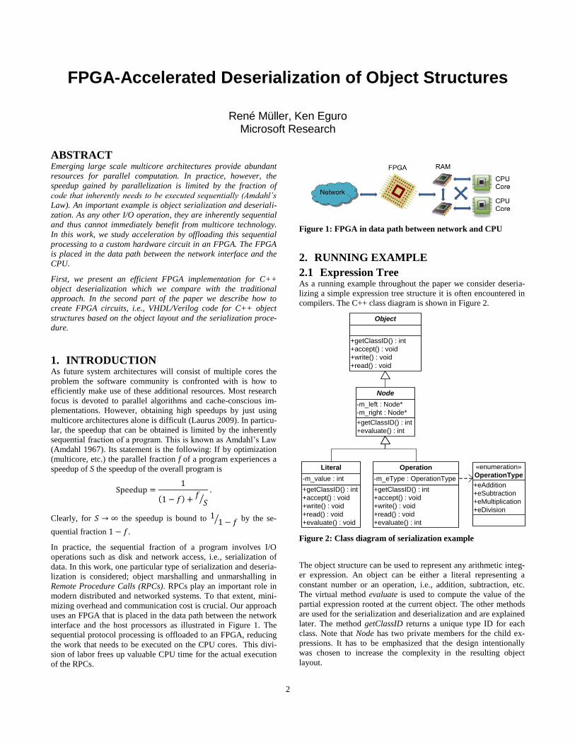
uses an FPGA that is placed in the data path between the network
interface and the host processors as illustrated in Figure 1. The
sequential protocol processing is offloaded to an FPGA, reducing
the work that needs to be executed on the CPU cores. This divi-
sion of labor frees up valuable CPU time for the actual execution
of the RPCs.
Figure 1: FPGA in data path between network and CPU
2. RUNNING EXAMPLE
2.1 Expression Tree As a running example throughout the paper we consider deseria-
lizing a simple expression tree structure it is often encountered in
compilers. The C++ class diagram is shown in Figure 2.
Figure 2: Class diagram of serialization example
The object structure can be used to represent any arithmetic integ-
er expression. An object can be either a literal representing a
constant number or an operation, i.e., addition, subtraction, etc.
The virtual method evaluate is used to compute the value of the
partial expression rooted at the current object. The other methods
are used for the serialization and deserialization and are explained
later. The method getClassID returns a unique type ID for each
class. Note that Node has two private members for the child ex-
pressions. It has to be emphasized that the design intentionally
was chosen to increase the complexity in the resulting object
layout.
+getClassID() : int
+accept() : void
+write() : void
+read() : void
Object
+getClassID() : int
+evaluate() : int
-m_left : Node*
-m_right : Node*
Node
+getClassID() : int
+accept() : void
+write() : void
+read() : void
+evaluate() : void
-m_value : int
Literal
+getClassID() : int
+accept() : void
+write() : void
+read() : void
+evaluate() : int
-m_eType : OperationType
Operation
+eAddition
+eSubtraction
+eMultiplication
+eDivision
«enumeration»
OperationType
3
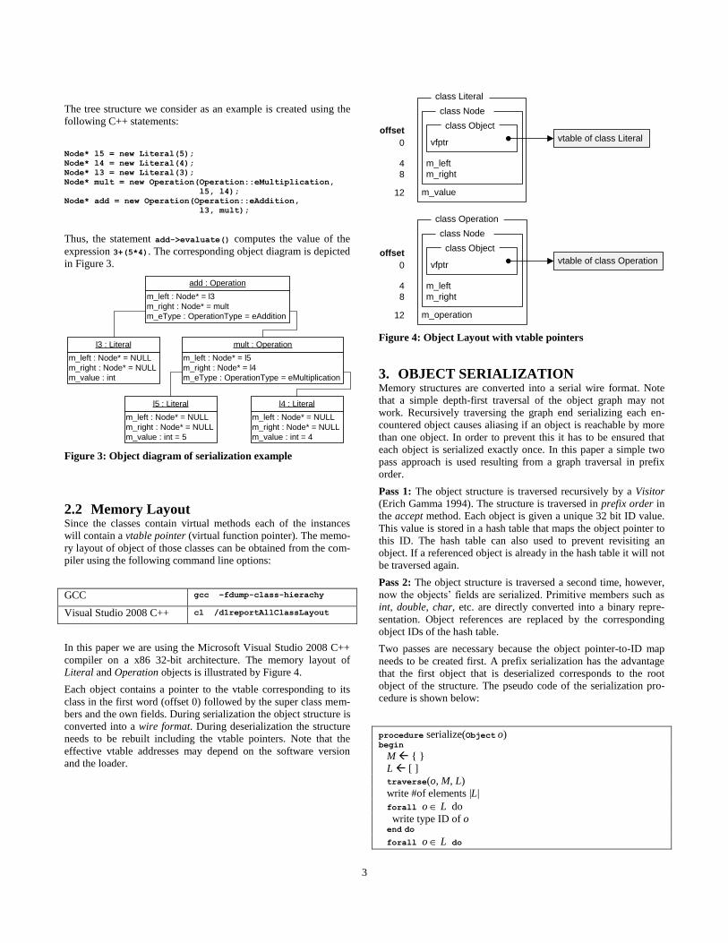
The tree structure we consider as an example is created using the
following C++ statements:
Node* l5 = new Literal(5);
Node* l4 = new Literal(4);
Node* l3 = new Literal(3);
Node* mult = new Operation(Operation::eMultiplication,
l5, l4);
Node* add = new Operation(Operation::eAddition,
l3, mult);
Thus, the statement add->evaluate() computes the value of the
expression 3+(5*4). The corresponding object diagram is depicted
in Figure 3.
Figure 3: Object diagram of serialization example
2.2 Memory Layout Since the classes contain virtual methods each of the instances
will contain a vtable pointer (virtual function pointer). The memo-
ry layout of object of those classes can be obtained from the com-
piler using the following command line options:
GCC gcc –fdump-class-hierachy
Visual Studio 2008 C++ cl /d1reportAllClassLayout
In this paper we are using the Microsoft Visual Studio 2008 C++
compiler on a x86 32-bit architecture. The memory layout of
Literal and Operation objects is illustrated by Figure 4.
Each object contains a pointer to the vtable corresponding to its
class in the first word (offset 0) followed by the super class mem-
bers and the own fields. During serialization the object structure is
converted into a wire format. During deserialization the structure
needs to be rebuilt including the vtable pointers. Note that the
effective vtable addresses may depend on the software version
and the loader.
Figure 4: Object Layout with vtable pointers
3. OBJECT SERIALIZATION Memory structures are converted into a serial wire format. Note
that a simple depth-first traversal of the object graph may not
work. Recursively traversing the graph end serializing each en-
countered object causes aliasing if an object is reachable by more
than one object. In order to prevent this it has to be ensured that
each object is serialized exactly once. In this paper a simple two
pass approach is used resulting from a graph traversal in prefix
order.
Pass 1: The object structure is traversed recursively by a Visitor
(Erich Gamma 1994). The structure is traversed in prefix order in
the accept method. Each object is given a unique 32 bit ID value.
This value is stored in a hash table that maps the object pointer to
this ID. The hash table can also used to prevent revisiting an
object. If a referenced object is already in the hash table it will not
be traversed again.
Pass 2: The object structure is traversed a second time, however,
now the objects’ fields are serialized. Primitive members such as
int, double, char, etc. are directly converted into a binary repre-
sentation. Object references are replaced by the corresponding
object IDs of the hash table.
Two passes are necessary because the object pointer-to-ID map
needs to be created first. A prefix serialization has the advantage
that the first object that is deserialized corresponds to the root
object of the structure. The pseudo code of the serialization pro-
cedure is shown below:
procedure serialize(Object o) begin M { }
L [ ]
traverse(o, M, L)
write #of elements |L| forall o L do
write type ID of o end do
forall o L do
m_left : Node* = NULL
m_right : Node* = NULL
m_value : int
l3 : Literal
m_left : Node* = NULL
m_right : Node* = NULL
m_value : int = 4
l4 : Literal
m_left : Node* = NULL
m_right : Node* = NULL
m_value : int = 5
l5 : Literal
m_left : Node* = l3
m_right : Node* = mult
m_eType : OperationType = eAddition
add : Operation
m_left : Node* = l5
m_right : Node* = l4
m_eType : OperationType = eMultiplication
mult : Operation
vfptr
class Object
m_left
m_right
class Node
m_value
class Literal
offset
0
4
8
12
vfptr
class Object
m_left
m_right
class Node
m_operation
class Operation
offset
0
4
8
12
vtable of class Literal
vtable of class Operation
4
forall members m of o do
if m is a primitive type
write m else
id lookup(m, M)
write id end if end do end do end
procedure traverse(Object o, Map M, List L) begin
id lookup(o, M)
if id = NIL do
id next object ID
put(o, id, M)
append(o, L)
forall object pointer members m of o do
traverse(m, M, L) end do end if end
Listing 1: Pseudo code of serialization algorithm
The serialized object structure thus consists of three parts:
Number of objects
List of Type IDs
List serialized objects (members)
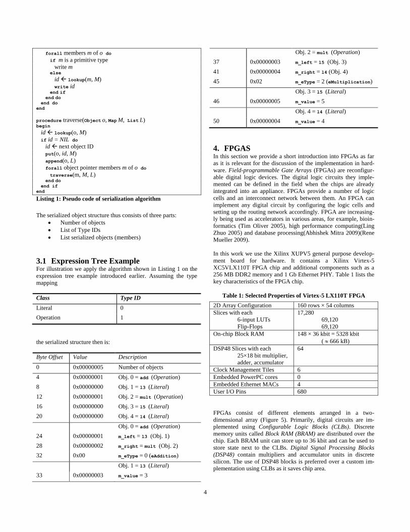
3.1 Expression Tree Example For illustration we apply the algorithm shown in Listing 1 on the
expression tree example introduced earlier. Assuming the type
mapping
Class Type ID
Literal 0
Operation 1
the serialized structure then is:
Byte Offset Value Description
0 0x00000005 Number of objects
4 0x00000001 Obj. 0 = add (Operation)
8 0x00000000 Obj. 1 = l3 (Literal)
12 0x00000001 Obj. 2 = mult (Operation)
16 0x00000000 Obj. 3 = l5 (Literal)
20 0x00000000 Obj. 4 = l4 (Literal)
Obj. 0 = add (Operation)
24 0x00000001 m_left = l3 (Obj. 1)
28 0x00000002 m_right = mult (Obj. 2)
32 0x00 m_eType = 0 (eAddition)
Obj. 1 = l3 (Literal)
33 0x00000003 m_value = 3
Obj. 2 = mult (Operation)
37 0x00000003 m_left = l5 (Obj. 3)
41 0x00000004 m_right = l4 (Obj. 4)
45 0x02 m_eType = 2 (eMultiplication)
Obj. 3 = l5 (Literal)
46 0x00000005 m_value = 5
Obj. 4 = l4 (Literal)
50 0x00000004 m_value = 4
4. FPGAS In this section we provide a short introduction into FPGAs as far
as it is relevant for the discussion of the implementation in hard-
ware. Field-programmable Gate Arrays (FPGAs) are reconfigur-
able digital logic devices. The digital logic circuits they imple-
mented can be defined in the field when the chips are already
integrated into an appliance. FPGAs provide a number of logic
cells and an interconnect network between them. An FPGA can
implement any digital circuit by configuring the logic cells and
setting up the routing network accordingly. FPGA are increasing-
ly being used as accelerators in various areas, for example, bioin-
formatics (Tim Oliver 2005), high performance computing(Ling
Zhuo 2005) and database processing(Abhishek Mitra 2009)(Rene
Mueller 2009).
In this work we use the Xilinx XUPV5 general purpose develop-
ment board for hardware. It contains a Xilinx Virtex-5
XC5VLX110T FPGA chip and additional components such as a
256 MB DDR2 memory and 1 Gb Ethernet PHY. Table 1 lists the
key characteristics of the FPGA chip.
Table 1: Selected Properties of Virtex-5 LX110T FPGA
2D Array Configuration 160 rows × 54 columns
Slices with each
6-input LUTs
Flip-Flops
17,280
69,120
69,120
On-chip Block RAM 148 × 36 kbit = 5328 kbit
( 666 kB)
DSP48 Slices with each
25×18 bit multiplier,
adder, accumulator
64
Clock Management Tiles 6
Embedded PowerPC cores 0
Embedded Ethernet MACs 4
User I/O Pins 680
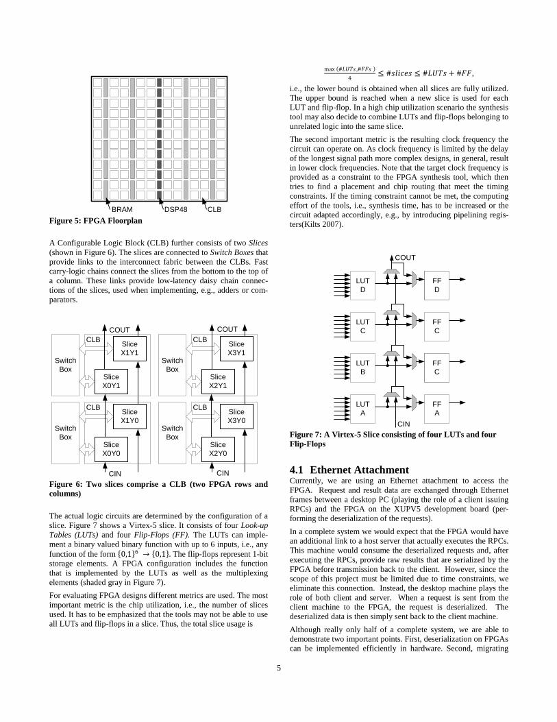
FPGAs consist of different elements arranged in a two-
dimensional array (Figure 5). Primarily, digital circuits are im-
plemented using Configurable Logic Blocks (CLBs). Discrete
memory units called Block RAM (BRAM) are distributed over the
chip. Each BRAM unit can store up to 36 kbit and can be used to
store state next to the CLBs. Digital Signal Processing Blocks
(DSP48) contain multipliers and accumulator units in discrete
silicon. The use of DSP48 blocks is preferred over a custom im-
plementation using CLBs as it saves chip area.
5
Figure 5: FPGA Floorplan
A Configurable Logic Block (CLB) further consists of two Slices
(shown in Figure 6). The slices are connected to Switch Boxes that
provide links to the interconnect fabric between the CLBs. Fast
carry-logic chains connect the slices from the bottom to the top of
a column. These links provide low-latency daisy chain connec-
tions of the slices, used when implementing, e.g., adders or com-
parators.
Figure 6: Two slices comprise a CLB (two FPGA rows and
columns)
The actual logic circuits are determined by the configuration of a
slice. Figure 7 shows a Virtex-5 slice. It consists of four Look-up
Tables (LUTs) and four Flip-Flops (FF). The LUTs can imple-
ment a binary valued binary function with up to 6 inputs, i.e., any
function of the form 0,1 6 → 0,1 . The flip-flops represent 1-bit
storage elements. A FPGA configuration includes the function
that is implemented by the LUTs as well as the multiplexing
elements (shaded gray in Figure 7).
For evaluating FPGA designs different metrics are used. The most
important metric is the chip utilization, i.e., the number of slices
used. It has to be emphasized that the tools may not be able to use
all LUTs and flip-flops in a slice. Thus, the total slice usage is
max #𝐿𝑈𝑇𝑠 ,#𝐹𝐹𝑠
4≤ #𝑠𝑙𝑖𝑐𝑒𝑠 ≤ #𝐿𝑈𝑇𝑠 + #𝐹𝐹,
i.e., the lower bound is obtained when all slices are fully utilized.
The upper bound is reached when a new slice is used for each
LUT and flip-flop. In a high chip utilization scenario the synthesis
tool may also decide to combine LUTs and flip-flops belonging to
unrelated logic into the same slice.
The second important metric is the resulting clock frequency the
circuit can operate on. As clock frequency is limited by the delay
of the longest signal path more complex designs, in general, result
in lower clock frequencies. Note that the target clock frequency is
provided as a constraint to the FPGA synthesis tool, which then
tries to find a placement and chip routing that meet the timing
constraints. If the timing constraint cannot be met, the computing
effort of the tools, i.e., synthesis time, has to be increased or the
circuit adapted accordingly, e.g., by introducing pipelining regis-
ters(Kilts 2007).
Figure 7: A Virtex-5 Slice consisting of four LUTs and four
Flip-Flops
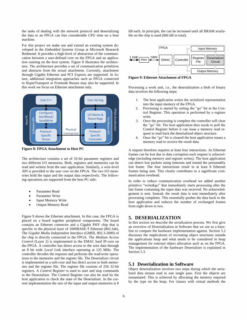
4.1 Ethernet Attachment Currently, we are using an Ethernet attachment to access the
FPGA. Request and result data are exchanged through Ethernet
frames between a desktop PC (playing the role of a client issuing
RPCs) and the FPGA on the XUPV5 development board (per-
forming the deserialization of the requests).
In a complete system we would expect that the FPGA would have
an additional link to a host server that actually executes the RPCs.
This machine would consume the deserialized requests and, after
executing the RPCs, provide raw results that are serialized by the
FPGA before transmission back to the client. However, since the
scope of this project must be limited due to time constraints, we
eliminate this connection. Instead, the desktop machine plays the
role of both client and server. When a request is sent from the
client machine to the FPGA, the request is deserialized. The
deserialized data is then simply sent back to the client machine.
Although really only half of a complete system, we are able to
demonstrate two important points. First, deserialization on FPGAs
can be implemented efficiently in hardware. Second, migrating
CLBBRAM DSP48
Slice
X0Y1
Slice
X1Y1Switch
BoxSlice
X2Y1
Slice
X3Y1Switch
Box
Slice
X0Y0
Slice
X1Y0Switch
BoxSlice
X2Y0
Slice
X3Y0Switch
Box
CLB CLB
CLB CLB
CIN CIN
COUT COUT
LUT
D
LUT
C
LUT
B
LUT
A
FF
A
FF
B
FF
C
FF
D
FF
C
FF
D
CIN
COUT
6
the tasks of dealing with the network protocol and deserializing
the data to an FPGA can free considerable CPU time on a host
machine.
For this project we make use and extend an existing system de-
veloped in the Embedded Systems Group at Microsoft Research
Redmond. It provides a high-level of abstraction of the communi-
cation between a user-defined core on the FPGA and an applica-
tion running on the host system. Figure 8 illustrates the architec-
ture. The architecture provides a set of communication primitives
and abstracts from the actual attachment. Currently, attachment
through Gigabit Ethernet and PCI Express are supported. In fu-
ture, additional integration approaches such as FPGA connected
to HyperTransport or Frontside Busses may also be supported. In
this work we focus on Ethernet attachment only.
Figure 8: FPGA Attachment to Host PC
The architecture contains a set of 32-bit parameter registers and
two different I/O memories. Both, registers and memories can be
read and written from the user application. Similarly, a wire-level
API is provided to the user core on the FPGA. The two I/O mem-
ories hold the input and the output data respectively. The follow-
ing operations are supported from the host PC side:
Parameter Read
Parameter Write
Input Memory Write
Output Memory Read
Figure 9 shows the Ethernet attachment. In this case, the FPGA is
placed on a board together peripheral components. The board
contains an Ethernet connector and a Gigabit PHY chip that is
specific to the physical layer of 1000BASE-T Ethernet (802.3ab).
The Gigabit Media Independent Interface (GMIII, 802.3-2000) of
the chip is directly connected to the FPGA. The Medium Access
Control (Layer 2) is implemented in the EMAC hard IP-core on
the FPGA. A controller has direct access to the wire data through
an 8 bit wide Local Link interface operating at 125 MHz. The
controller decodes the requests and performs the read/write opera-
tions to the memories and the register file. The Deserializer circuit
is implemented as a soft-core and has direct access to both memo-
ries and the register file. The register file consists of 256 32-bit
registers. A Control Register is used to start and stop commands
to the Deserializer. The Control Register can also be read by the
host application to check the state of the Deserializer. In the cur-
rent implementation the size of the input and output memories is 8
kB each. In principle, the can be increased until all BRAM availa-
ble on the chip is used (666 kB in total).
Figure 9: Ethernet Attachment of FPGA
Processing a work unit, i.e., the deserialization a blob of binary
data involves the following steps:
1. The host application writes the serialized representation
into the input memory of the FPGA.
2. Processing is started by setting the ―go‖ bit in the Con-
trol Register. This operation is performed by a register
write.
3. Once the processing is complete the controller will clear
the ―go‖ bit. The host application thus needs to poll the
Control Register before it can issue a memory read re-
quest to read back the deserialized object structure.
4. Once the ―go‖ bit is cleared the host application issues a
memory read to receive the result data.
A request therefore requires at least four interactions. As Ethernet
frames can be lost due to data corruption each request is acknowl-
edge (including memory and register writes). The host application
can detect lost packets using timeouts and resend the presumably
lost frame. The four interactions result in at least 8 Ethernet
frames being sent. This clearly contributes to a significant com-
munication overhead.
In order to reduce communication overhead we added another
primitive ―write&go‖ that immediately starts processing after the
last frame containing the input data was received. No acknowled-
gement is sent. Instead, the result data is sent immediately after
processing completes. This essentially pushes the data back to the
host application and reduces the number of exchanged frames
from eight down to two.
5. DESERIALIZATION In this section we describe the serialization process. We first give
an overview of Deserialization in Software that we use as a base-
line to compare the hardware implementation against. Section 5.2
discusses the implications of recreating object structures outside
the applications heap and what needs to be considered in heap
management for external object allocation such as on the FPGA.
The implementation of the hardware Deserializer is explained in
Section 5.3.
5.1 Deserialization in Software Object deserialization involves two steps during which the seria-
lized data stream read in one single pass. First the objects are
instantiated. This is achieved by allocating the memory required
by the type on the heap. For classes with virtual methods the
FPG
A A
ccelerator
Ho
st P
C
User C++
Soft
war
e A
PI
User Verilog
Ha
rdw
are AP
I
I/O Mems & Param Regs
Protocol-Specific Driver
Configure/ SendRead/ SendWrite
Protocol-Specific
Controller
PhysicalConnection
Deserializer
CircuitPHY
1 GbEEMAC
GMIIController
Register
File
Input Memory
Output Memory
FPGA
7
vtable pointers of the instances need to be set. The pseudo-code of
object deserialization is shown below:
Phase 1:
i 0
L [ ]
n readNumObjectsFromStream( )
forall n objects in stream
t readTypeFromStream( )
o allocateObjectOfType(t)
setVtablePointer(o)
L[i] o
i i +1
Phase 2:
forall 0 ≤ i ≤ n
L[i].read(stream)
In a second phase the object members are initialized. Since the
vtable pointers are already setup object deserialization can be
done by calling a virtual method Object::read(char
*buffer, int *pos, Serializer *s) defined in the base
class of all objects. The actual classes implement object deseriali-
zation. The implementation for Literal class is:
void Literal::read(char *buffer, int *pos,
const Serializer *s)
{
m_value = *(int*)(buffer+*pos);
*pos += 4; // sizeof(m_value) == 4 bytes
}
For object references the Serializer instance is used to lookup the
object pointer for a given object ID. Here the ID corresponds to
the index into the list L (see above). For example, for Operation
the read method looks as follows:
void Operation::read(char *buffer, int *pos,
const Serializer *s)
{
int left = *(int*)(&buffer[*pos]);
*pos += 4; // size of object ID on stream
int right = *(int*)(&buffer[*pos]);
*pos += 4; // size of object ID on stream
// look-up Node for IDs
m_left = dynamic_cast<Node*>(s->getObject(left));
m_right = dynamic_cast<Node*>(s->getObject(right));
// set operation type (Addition, etc.)
m_eType = (OperationType)buffer[*pos];
(*pos)++; // sizeof(m_eType) == 1 byte
}
5.2 Heap Management When invoking the new operator the necessary bytes for the in-
stance are allocated on the heap during a call to malloc. Note that
in general malloc is free to place object at any memory location.
In order to simplify the write-back to main memory only one
single memory region should be copied. Thus, the objects have to
be allocated in a contiguous area on the FPGA.
A second important aspect is that object pointers need to be setup
such that they point to the appropriate memory locations after the
deserialized structure is copied back from the network to the heap
memory. Updating the pointers, i.e., pointer relocation after the
write back would have a significant impact on performance.
We address the two problems by preallocating a contiguous mem-
ory region in virtual memory space, e.g., 8 kB that can hold all
result data. In each deserialization request we also send the start
address of this result buffer along. This allows the FPGA to setup
the pointers correctly such that the result structure can be trans-
ferred to the preallocated buffer using memcpy.
It is important to point out that since these objects are allocated
outside the usual C++ runtime special care needs to be taken when
deleting the instances or modifying the structure, for example, by
adding more instances.
To this extend the standard C++ new and delete operators have to
be overwritten such that they reflect this custom memory man-
agement. An additional possibility is to replace the delete operator
by an empty implementation when assuming that the data struc-
ture is freed altogether, e.g., after an RPC completes. In our im-
plementation we overwrite the two operators in the Object base
class as follows:
void * Object::operator new(unsigned int size)
{
return preallocate_memory(size);
}
void Object::operator delete(void *buf)
{
// do nothing, ignore 'delete'
}
5.3 Deserialization in Hardware In this section we describe the Deserializer core implemented in
Verilog HDL. The Deserializer is added as a user core to the
Ethernet attachment architecture. Figure 10 depicts the structure
of the Deserializer core.
Input Memory BRAM
Output Memory BRAM
LiteralOperation
objPtr
2N
objType
2N
currHeapPtrcurrObject
lastObjectStream
Reader
Finite State Machine (FSM)
Cycle Ctr
ControlError
255254253
LiteralOperation
vtable[2]vtable[3]vtable[4]
vtable[252]
01234
252
Para
me
ter
Reg
iste
rs
Register File
copy during
initialization
BRAM
Flip-flop Register
Control Logic
Legend:
outMemAddr
8
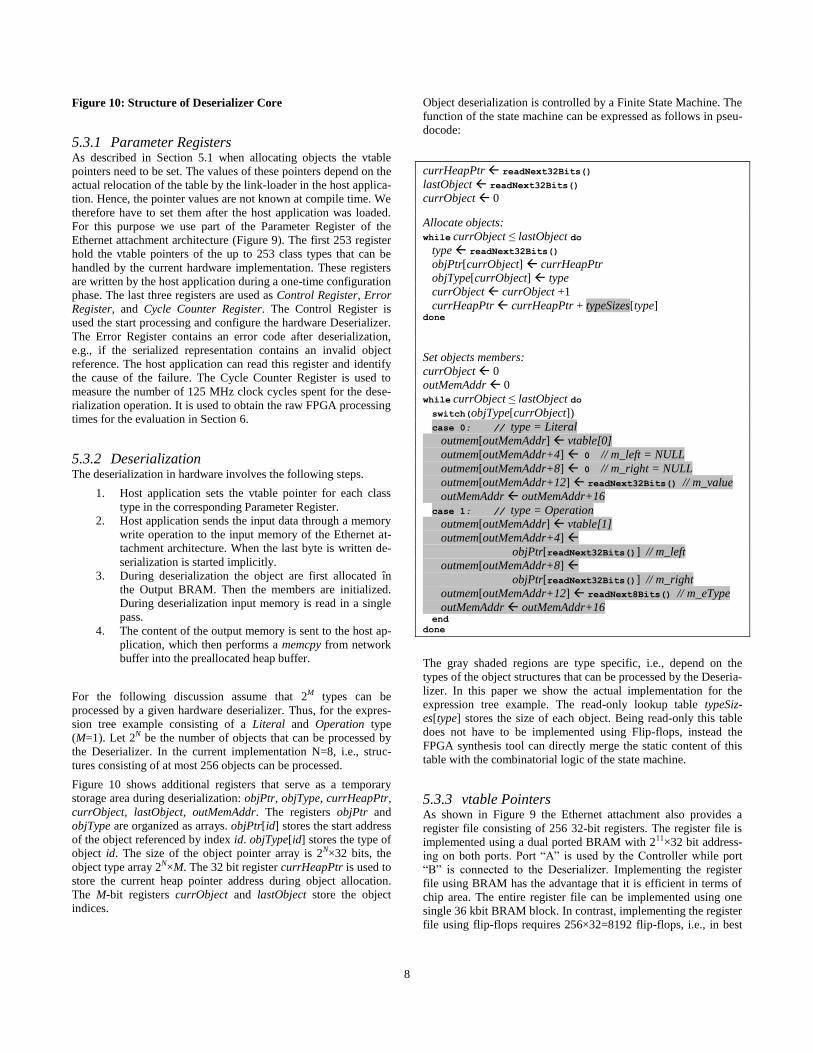
Figure 10: Structure of Deserializer Core
5.3.1 Parameter Registers As described in Section 5.1 when allocating objects the vtable
pointers need to be set. The values of these pointers depend on the
actual relocation of the table by the link-loader in the host applica-
tion. Hence, the pointer values are not known at compile time. We
therefore have to set them after the host application was loaded.
For this purpose we use part of the Parameter Register of the
Ethernet attachment architecture (Figure 9). The first 253 register
hold the vtable pointers of the up to 253 class types that can be
handled by the current hardware implementation. These registers
are written by the host application during a one-time configuration
phase. The last three registers are used as Control Register, Error
Register, and Cycle Counter Register. The Control Register is
used the start processing and configure the hardware Deserializer.
The Error Register contains an error code after deserialization,
e.g., if the serialized representation contains an invalid object
reference. The host application can read this register and identify
the cause of the failure. The Cycle Counter Register is used to
measure the number of 125 MHz clock cycles spent for the dese-
rialization operation. It is used to obtain the raw FPGA processing
times for the evaluation in Section 6.
5.3.2 Deserialization The deserialization in hardware involves the following steps.
1. Host application sets the vtable pointer for each class
type in the corresponding Parameter Register.
2. Host application sends the input data through a memory
write operation to the input memory of the Ethernet at-
tachment architecture. When the last byte is written de-
serialization is started implicitly.
3. During deserialization the object are first allocated în
the Output BRAM. Then the members are initialized.
During deserialization input memory is read in a single
pass.
4. The content of the output memory is sent to the host ap-
plication, which then performs a memcpy from network
buffer into the preallocated heap buffer.
For the following discussion assume that 2M types can be
processed by a given hardware deserializer. Thus, for the expres-
sion tree example consisting of a Literal and Operation type
(M=1). Let 2N be the number of objects that can be processed by
the Deserializer. In the current implementation N=8, i.e., struc-
tures consisting of at most 256 objects can be processed.
Figure 10 shows additional registers that serve as a temporary
storage area during deserialization: objPtr, objType, currHeapPtr,
currObject, lastObject, outMemAddr. The registers objPtr and
objType are organized as arrays. objPtr[id] stores the start address
of the object referenced by index id. objType[id] stores the type of
object id. The size of the object pointer array is 2N×32 bits, the
object type array 2N×M. The 32 bit register currHeapPtr is used to
store the current heap pointer address during object allocation.
The M-bit registers currObject and lastObject store the object
indices.
Object deserialization is controlled by a Finite State Machine. The
function of the state machine can be expressed as follows in pseu-
docode:
currHeapPtr readNext32Bits()
lastObject readNext32Bits()
currObject 0
Allocate objects:
while currObject ≤ lastObject do
type readNext32Bits()
objPtr[currObject] currHeapPtr
objType[currObject] type
currObject currObject +1
currHeapPtr currHeapPtr + typeSizes[type] done
Set objects members:
currObject 0
outMemAddr 0
while currObject ≤ lastObject do
switch(objType[currObject])
case 0: // type = Literal
outmem[outMemAddr] vtable[0]
outmem[outMemAddr+4] 0 // m_left = NULL
outmem[outMemAddr+8] 0 // m_right = NULL
outmem[outMemAddr+12] readNext32Bits() // m_value
outMemAddr outMemAddr+16
case 1: // type = Operation
outmem[outMemAddr] vtable[1]
outmem[outMemAddr+4]
objPtr[readNext32Bits()] // m_left
outmem[outMemAddr+8]
objPtr[readNext32Bits()] // m_right
outmem[outMemAddr+12] readNext8Bits() // m_eType
outMemAddr outMemAddr+16 end done
The gray shaded regions are type specific, i.e., depend on the
types of the object structures that can be processed by the Deseria-
lizer. In this paper we show the actual implementation for the
expression tree example. The read-only lookup table typeSiz-
es[type] stores the size of each object. Being read-only this table
does not have to be implemented using Flip-flops, instead the
FPGA synthesis tool can directly merge the static content of this
table with the combinatorial logic of the state machine.
5.3.3 vtable Pointers As shown in Figure 9 the Ethernet attachment also provides a
register file consisting of 256 32-bit registers. The register file is
implemented using a dual ported BRAM with 211×32 bit address-
ing on both ports. Port ―A‖ is used by the Controller while port
―B‖ is connected to the Deserializer. Implementing the register
file using BRAM has the advantage that it is efficient in terms of
chip area. The entire register file can be implemented using one
single 36 kbit BRAM block. In contrast, implementing the register
file using flip-flops requires 256×32=8192 flip-flops, i.e., in best
9
case 2048 FPGA slices. This corresponds to 11.8% of the chip
space on our FPGA chip.
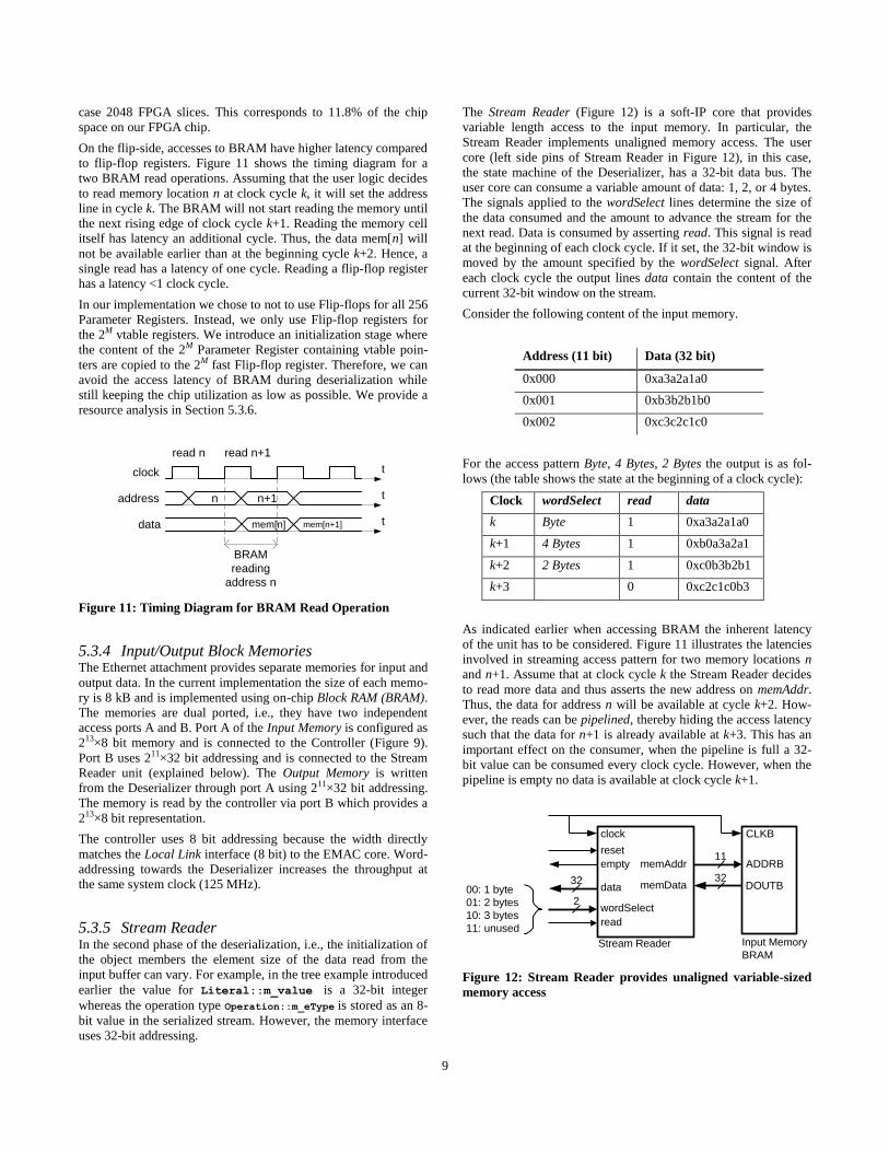
On the flip-side, accesses to BRAM have higher latency compared
to flip-flop registers. Figure 11 shows the timing diagram for a
two BRAM read operations. Assuming that the user logic decides
to read memory location n at clock cycle k, it will set the address
line in cycle k. The BRAM will not start reading the memory until
the next rising edge of clock cycle k+1. Reading the memory cell
itself has latency an additional cycle. Thus, the data mem[n] will
not be available earlier than at the beginning cycle k+2. Hence, a
single read has a latency of one cycle. Reading a flip-flop register
has a latency <1 clock cycle.
In our implementation we chose to not to use Flip-flops for all 256
Parameter Registers. Instead, we only use Flip-flop registers for
the 2M vtable registers. We introduce an initialization stage where
the content of the 2M Parameter Register containing vtable poin-
ters are copied to the 2M fast Flip-flop register. Therefore, we can
avoid the access latency of BRAM during deserialization while
still keeping the chip utilization as low as possible. We provide a
resource analysis in Section 5.3.6.
tclock
address tn
data tmem[n] mem[n+1]
n+1
read n read n+1
BRAM
reading
address n
Figure 11: Timing Diagram for BRAM Read Operation
5.3.4 Input/Output Block Memories The Ethernet attachment provides separate memories for input and
output data. In the current implementation the size of each memo-
ry is 8 kB and is implemented using on-chip Block RAM (BRAM).
The memories are dual ported, i.e., they have two independent
access ports A and B. Port A of the Input Memory is configured as
213×8 bit memory and is connected to the Controller (Figure 9).
Port B uses 211×32 bit addressing and is connected to the Stream
Reader unit (explained below). The Output Memory is written
from the Deserializer through port A using 211×32 bit addressing.
The memory is read by the controller via port B which provides a
213×8 bit representation.
The controller uses 8 bit addressing because the width directly
matches the Local Link interface (8 bit) to the EMAC core. Word-
addressing towards the Deserializer increases the throughput at
the same system clock (125 MHz).
5.3.5 Stream Reader In the second phase of the deserialization, i.e., the initialization of
the object members the element size of the data read from the
input buffer can vary. For example, in the tree example introduced
earlier the value for Literal::m_value is a 32-bit integer
whereas the operation type Operation::m_eType is stored as an 8-
bit value in the serialized stream. However, the memory interface
uses 32-bit addressing.
The Stream Reader (Figure 12) is a soft-IP core that provides
variable length access to the input memory. In particular, the
Stream Reader implements unaligned memory access. The user
core (left side pins of Stream Reader in Figure 12), in this case,
the state machine of the Deserializer, has a 32-bit data bus. The
user core can consume a variable amount of data: 1, 2, or 4 bytes.
The signals applied to the wordSelect lines determine the size of
the data consumed and the amount to advance the stream for the
next read. Data is consumed by asserting read. This signal is read
at the beginning of each clock cycle. If it set, the 32-bit window is
moved by the amount specified by the wordSelect signal. After
each clock cycle the output lines data contain the content of the
current 32-bit window on the stream.
Consider the following content of the input memory.
Address (11 bit) Data (32 bit)
0x000 0xa3a2a1a0
0x001 0xb3b2b1b0
0x002 0xc3c2c1c0
For the access pattern Byte, 4 Bytes, 2 Bytes the output is as fol-
lows (the table shows the state at the beginning of a clock cycle):
Clock wordSelect read data
k Byte 1 0xa3a2a1a0
k+1 4 Bytes 1 0xb0a3a2a1
k+2 2 Bytes 1 0xc0b3b2b1
k+3 0 0xc2c1c0b3
As indicated earlier when accessing BRAM the inherent latency
of the unit has to be considered. Figure 11 illustrates the latencies
involved in streaming access pattern for two memory locations n
and n+1. Assume that at clock cycle k the Stream Reader decides
to read more data and thus asserts the new address on memAddr.
Thus, the data for address n will be available at cycle k+2. How-
ever, the reads can be pipelined, thereby hiding the access latency
such that the data for n+1 is already available at k+3. This has an
important effect on the consumer, when the pipeline is full a 32-
bit value can be consumed every clock cycle. However, when the
pipeline is empty no data is available at clock cycle k+1.
Figure 12: Stream Reader provides unaligned variable-sized
memory access
clock
data
wordSelect
read
empty
32
2
Stream Reader
memAddr
32memData
11ADDRB
CLKB
DOUTB
Input Memory
BRAM
00: 1 byte
01: 2 bytes
10: 3 bytes
11: unused
reset
10
One solution to prevent the user core from reading invalid data is
to use a pushback mechanism. That is, to tell the consumer that
the data lines contain no valid data at clock cycle k+1. This ap-
proach not only negatively effects performance as no work can be
done in that cycle, but it also adds more complexity to the logic of
the user component. In this paper we chose a different approach.
We added a 96-bit buffer to the stream reader. The buffer is im-
plemented using fast flip-flop registers. It can be easily shown that
96 bits or equivalently three 32-bit words (=12 bytes) is the mini-
mum size required to bridge the latency from starting filling up
the pipeline until the first data item can be retrieved from the
BRAM. Since both the output data port of the Stream Reader and
the memory have the same size, a sustained read rate of 32 bits
per clock cycle (=500 MB/s) can be easily achieved. The buffer is
filled as soon as the reset signal is cleared. The empty signal
indicates the user component that the data line is not ready. Al-
though this can be considered a pushback too, empty is only low
after a reset until the buffer is full. Once empty is low the data
lines stays valid until the next reset. The user component thus can
use the empty signal together with the reset signal as a ―ready
after reset‖ condition. After that the empty signal can be ignored.
5.3.6 Resource Usage The resource usage of the Deserializer circuit can be expressed in
terms of LUT and Flip-flop usage. The overall chip utilization is
expressed in the number of used slices which consists of both
LUTs and Flip-flops. As described in Section 4 the FPGA synthe-
sis tool performs heavy optimization which makes the number of
used LUTs difficult to predict. Furthermore it can decide to com-
bine unrelated circuits into the same slice. Thus, we provide num-
bers for the overall chip usage of the entire FPGA circuit, i.e., the
Deserializer as well as Ethernet attachment (Controller, etc.).
Flip-flops representing basic bit storage elements, however, are
easier to predict. Assuming that the Deserializer is able to process
2M types and structures consisting of at most 2N objects the num-
ber of Flip-flops used for each register is:
#size-dependent Flip-flops
= 2𝑁 ∙ 32 objPtr
+ 2𝑁 ∙ 𝑀 objType
+ 2𝑀 ∙ 32 vtable
Register
+ 2𝑀 currObject+
lastObject
This analysis only includes the Flip-flops that depend on the
problem size, i.e., the parameters M and N. For M=1 and N=8,
8514 Flip-flops are necessary. This corresponds to 12.3% of the
chip resources. Flips-flops that are independent of these parame-
ters, such as currHeapPtr and outMemAddr are accounted for the
in the overall utilization.
Table 2 shows the overall chip utilization of the complete FPGA
design (Deserializer and Ethernet attachment) on our
XC5VLX110T chip. This data is reported at the end of the design
flow process by the Xilinx ISE 10.1.03 synthesis tool. Both the
Flip-flop and the LUT utilization are comparatively low. The fact
that the slice utilization is almost the sum of the register and LUT
utilizations indicates that there is not much overlap between logic
and registers. Nevertheless, the overall chip utilization is <25%.
For that matter, the resource utilization could be further reduced
by migrating the objPtr and objType storage areas into BRAM
and eliminating the redundant vtable pointer registers. These
optimizations were not considered in this investigation merely to
simplify implementation.
As an estimate of the actual resource consumption of the Deseria-
lizer itself we also list the results from the Map Report. The Map
stage of the FPGA design flow maps high-level primitives to
device-primitives. This phase occurs before Place & Route and
hence, the utilization numbers are not yet final. Nevertheless, they
represent the last stage in the work flow where the design hie-
rarchy still exists. Table 3 shows the chip utilization after the Map
stage. The table indicates that the Deserializer itself uses 14% of
the chip space and together with the Stream Reader 16% of the
chip. Considering these numbers alone it seems to be possible (in
theory) to instantiate approximately 6 Deserializer cores on the
currently targeted chip.
Table 2: Resource Utilization of Complete Design
Used Chip utilization
Flip-flop Registers 10,311 14%
LUTs 6,463 9%
Occupied Slices 3,874 22%
36 kb BRAM Blocks
Total Memory
9
40.5 kB
6%
6%
Input/Output Blocks 30 4%
Table 3: Resource Utilization of Deserializer and Stream
Reader after Map Stage
Flip-
Flops
LUTs Slices
Deserializer
(without Stream Reader)
8,714
(13%)
3,372
(5%)
2,488
(14%)
Stream Reader 115
(0.2%)
706
(1%)
330
(2%)
The second metric used is the clock speed the circuit can operate
on. We have been able to synthesize and operate the circuit at the
full 125 MHz of the Gigabit Ethernet MAC. For simplicity we
used one single clock region whose clock is given by the Ethernet
MAC. 1 In principle, it should be possible to operate the Deseria-
lizer, including the B port of the Input Memory and the A port of
the Output Memory at a higher clock rate. However, this has not
been experimentally verified yet.
6. EVALUATION In this section we perform a performance evaluation. We compare
the hardware implementation against a traditional software solu-
tion. We evaluate the overall end-to-end performance, as well as
1 Actually, two clocks are used. Next to the 125 MHz system
clock a 200 MHz reference clock is used for the IDELAY and
IDELAY controller respectively. The reference clock is used to
drive the tapped delay line for the RX clock of EMAC GMII
interface.
11
the time spent for the deserialization alone. First, we assess the
communication overhead of the network link between two PCs
and between a PC and a FPGA board. This comparison will allow
us to quantify the time spent by a server not necessarily
processing the request, but simply moving a request through
various levels of the network stack and operating system. After
that, we will look into the execution time of the serialization and
deserialization itself.
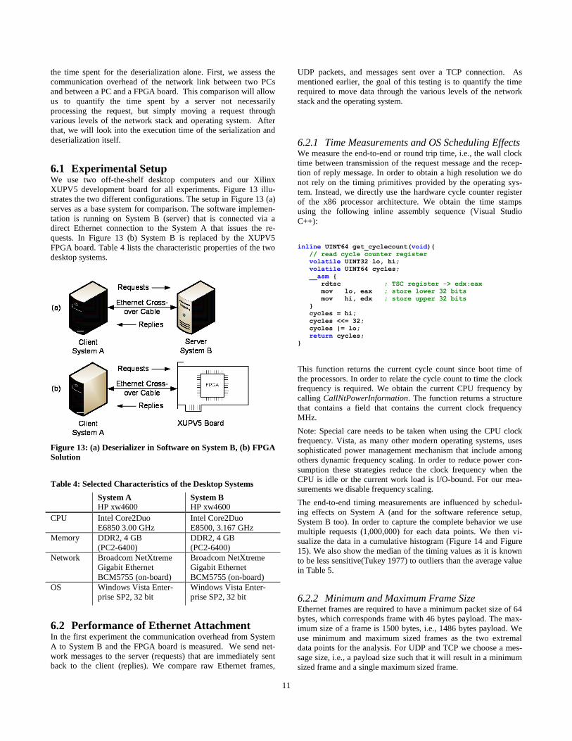
6.1 Experimental Setup We use two off-the-shelf desktop computers and our Xilinx
XUPV5 development board for all experiments. Figure 13 illu-
strates the two different configurations. The setup in Figure 13 (a)
serves as a base system for comparison. The software implemen-
tation is running on System B (server) that is connected via a
direct Ethernet connection to the System A that issues the re-
quests. In Figure 13 (b) System B is replaced by the XUPV5
FPGA board. Table 4 lists the characteristic properties of the two
desktop systems.
Figure 13: (a) Deserializer in Software on System B, (b) FPGA
Solution
Table 4: Selected Characteristics of the Desktop Systems
System A
HP xw4600 System B
HP xw4600
CPU Intel Core2Duo
E6850 3.00 GHz
Intel Core2Duo
E8500, 3.167 GHz
Memory DDR2, 4 GB
(PC2-6400)
DDR2, 4 GB
(PC2-6400)
Network Broadcom NetXtreme
Gigabit Ethernet
BCM5755 (on-board)
Broadcom NetXtreme
Gigabit Ethernet
BCM5755 (on-board)
OS Windows Vista Enter-
prise SP2, 32 bit
Windows Vista Enter-
prise SP2, 32 bit
6.2 Performance of Ethernet Attachment In the first experiment the communication overhead from System
A to System B and the FPGA board is measured. We send net-
work messages to the server (requests) that are immediately sent
back to the client (replies). We compare raw Ethernet frames,
UDP packets, and messages sent over a TCP connection. As
mentioned earlier, the goal of this testing is to quantify the time
required to move data through the various levels of the network
stack and the operating system.
6.2.1 Time Measurements and OS Scheduling Effects We measure the end-to-end or round trip time, i.e., the wall clock
time between transmission of the request message and the recep-
tion of reply message. In order to obtain a high resolution we do
not rely on the timing primitives provided by the operating sys-
tem. Instead, we directly use the hardware cycle counter register
of the x86 processor architecture. We obtain the time stamps
using the following inline assembly sequence (Visual Studio
C++):
inline UINT64 get_cyclecount(void){
// read cycle counter register
volatile UINT32 lo, hi;
volatile UINT64 cycles;
__asm {
rdtsc ; TSC register -> edx:eax
mov lo, eax ; store lower 32 bits
mov hi, edx ; store upper 32 bits
}
cycles = hi;
cycles <<= 32;
cycles |= lo;
return cycles;
}
This function returns the current cycle count since boot time of
the processors. In order to relate the cycle count to time the clock
frequency is required. We obtain the current CPU frequency by
calling CallNtPowerInformation. The function returns a structure
that contains a field that contains the current clock frequency
MHz.
Note: Special care needs to be taken when using the CPU clock
frequency. Vista, as many other modern operating systems, uses
sophisticated power management mechanism that include among
others dynamic frequency scaling. In order to reduce power con-
sumption these strategies reduce the clock frequency when the
CPU is idle or the current work load is I/O-bound. For our mea-
surements we disable frequency scaling.
The end-to-end timing measurements are influenced by schedul-
ing effects on System A (and for the software reference setup,
System B too). In order to capture the complete behavior we use
multiple requests (1,000,000) for each data points. We then vi-
sualize the data in a cumulative histogram (Figure 14 and Figure
15). We also show the median of the timing values as it is known
to be less sensitive(Tukey 1977) to outliers than the average value
in Table 5.
6.2.2 Minimum and Maximum Frame Size Ethernet frames are required to have a minimum packet size of 64
bytes, which corresponds frame with 46 bytes payload. The max-
imum size of a frame is 1500 bytes, i.e., 1486 bytes payload. We
use minimum and maximum sized frames as the two extremal
data points for the analysis. For UDP and TCP we choose a mes-
sage size, i.e., a payload size such that it will result in a minimum
sized frame and a single maximum sized frame.
12
6.2.3 Ethernet Frames on Desktop Systems Unicast raw Ethernet frames are sent from System A to System B.
After receiving the frame System B swaps source and destination
address of the frame and sends it back to System A. This bench-
mark provides the baseline for the offloaded processing as it
captures only the communication overhead.
We send raw Ethernet frames through the Virtual Network driver
VPCNetS2 provided by Microsoft Virtual PC 2007. This driver is
added at the bottom of the network stack and is able create a
virtual network interface with its own MAC address. We use this
new virtual device to transmit and receive Ethernet frames. The
code base for harnessing the virtual network device comes from
Giano [10]. The code uses asynchronous calls, and makes use of
the efficient I/O completion queues of the Windows API.
To isolate the systems under test from external noise we discon-
nected the nodes from the corporate network and establish a direct
connection between the nodes through a cross-over cable. Fur-
thermore we disabled the IP and Microsoft Client Protocols on
both systems for the Broadcom network device. This suppresses
occasional ARP requests sent by the hosts.
6.2.4 Ethernet Frames in FPGA System For the FPGA setup we use a special purpose FPGA design. We
modify the Ethernet controller (Figure 9) such that as soon as the
frame leaves the EMAC core to the Controller (after the entire
frame was received and the CRC verified) it is resent with the
source and destination addresses exchanged. The Local Link
interface of the EMAC core is 8 bit wide and streams the frame to
the user controller. The controller waits 12 cycles until it has seen
source and destination address. It then swaps the 6 bytes and
sends the packet immediately back to the EMAC core through the
transmit Local Link interface. This results in a possibly shortest
round trip time:
2 ∙ #frame bytes + 12 1
125 MHz
This number doubles the number of frame bytes to account for the
fact that 1) the entire request packet is received by the FPGA
before being sent back and 2) the entire reply packet must be
received by the PC’s NIC before being passed up to the driver.
This is not four times the number of frame bytes because the time
required by the PC’s NIC to send the request packet overlaps the
interval in which the FPGA is receiving the request packet and
vice-versa for the reply packet. For 64 byte Ethernet frames the
minimum round-trip time is 1.12µs. For maximum sized 1500
byte frames the time for the frame reflection is 24µs.
6.2.5 UDP Packets In order evaluate the impact of the IP layer and a packet-oriented
transport layer on the overall performance we also implement the
ping-pong message exchange on UDP. We test this setup only
with the desktop hosts shown in Figure 13 (a). A one byte UDP
datagram results in a 66 byte Ethernet frame. The maximal UDP
payload size such that no IP fragmentation occurs is 1450 bytes.
6.2.6 TCP Fragments Messages sent over a TCP socket are used to evaluate the perfor-
mance impact of a connection oriented transport on layer 4 in the
network stack. A one-byte send operation on a TCP socket results
in a 78 byte Ethernet frame (after the connection has be setup).
The payload can be increased up to 1435 bytes until IP fragmenta-
tion occurs.
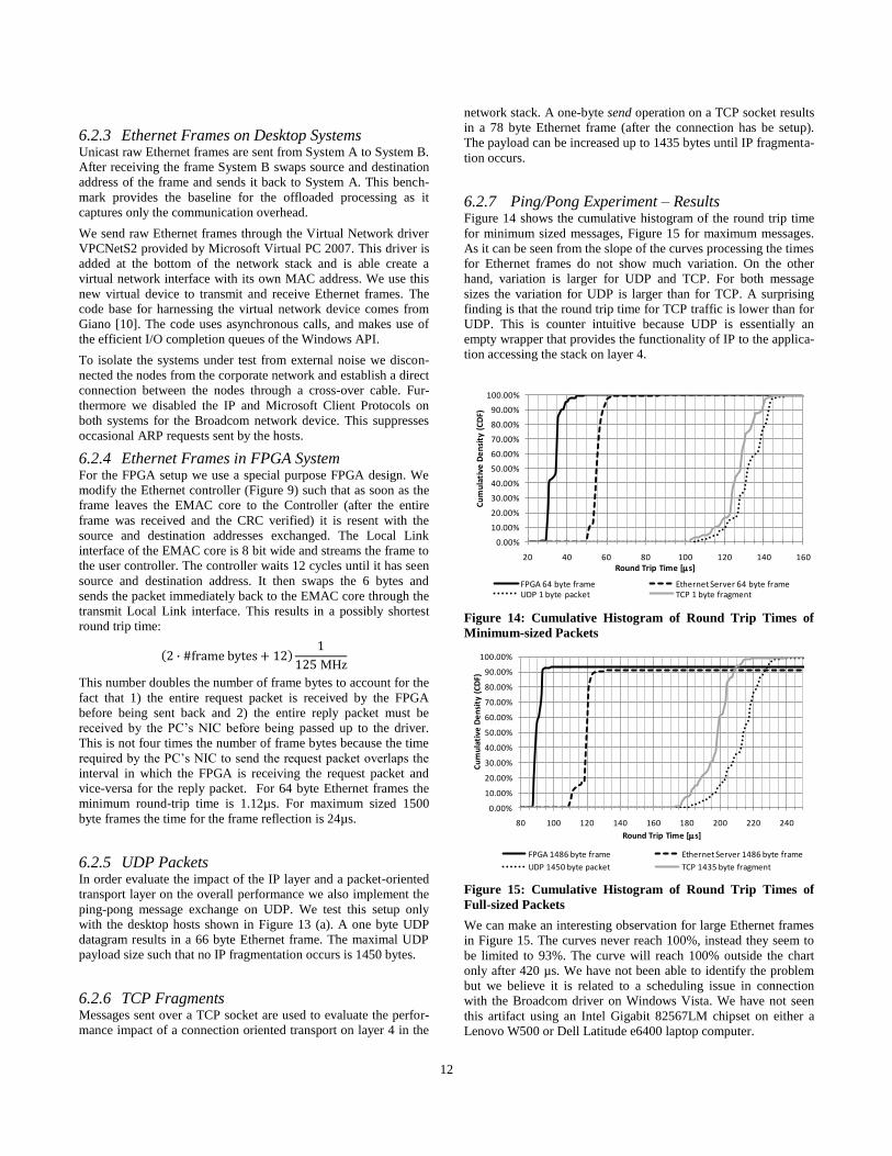
6.2.7 Ping/Pong Experiment – Results Figure 14 shows the cumulative histogram of the round trip time
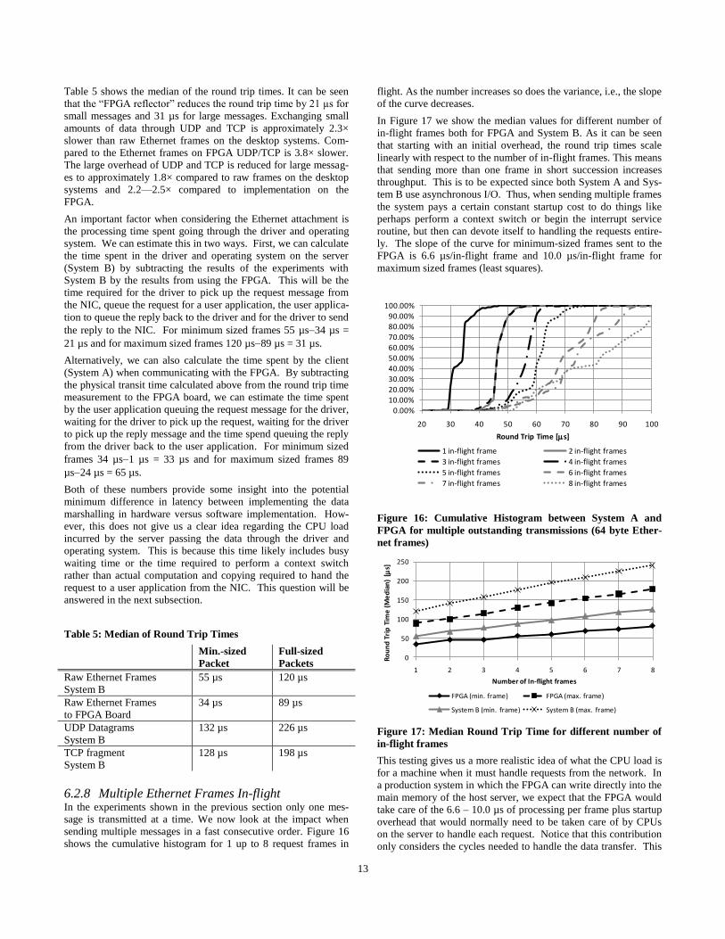
for minimum sized messages, Figure 15 for maximum messages.
As it can be seen from the slope of the curves processing the times
for Ethernet frames do not show much variation. On the other
hand, variation is larger for UDP and TCP. For both message
sizes the variation for UDP is larger than for TCP. A surprising
finding is that the round trip time for TCP traffic is lower than for
UDP. This is counter intuitive because UDP is essentially an
empty wrapper that provides the functionality of IP to the applica-
tion accessing the stack on layer 4.
Figure 14: Cumulative Histogram of Round Trip Times of
Minimum-sized Packets
Figure 15: Cumulative Histogram of Round Trip Times of
Full-sized Packets
We can make an interesting observation for large Ethernet frames
in Figure 15. The curves never reach 100%, instead they seem to
be limited to 93%. The curve will reach 100% outside the chart
only after 420 µs. We have not been able to identify the problem
but we believe it is related to a scheduling issue in connection
with the Broadcom driver on Windows Vista. We have not seen
this artifact using an Intel Gigabit 82567LM chipset on either a
Lenovo W500 or Dell Latitude e6400 laptop computer.
0.00%
10.00%
20.00%
30.00%
40.00%
50.00%
60.00%
70.00%
80.00%
90.00%
100.00%
20 40 60 80 100 120 140 160
Cu
mu
lati
ve D
en
sity
(C
DF)
Round Trip Time [s]
FPGA 64 byte frame Ethernet Server 64 byte frameUDP 1 byte packet TCP 1 byte fragment
0.00%
10.00%
20.00%
30.00%
40.00%
50.00%
60.00%
70.00%
80.00%
90.00%
100.00%
80 100 120 140 160 180 200 220 240
Cu
mu
lati
ve D
en
sity
(C
DF)
Round Trip Time [s]
FPGA 1486 byte frame Ethernet Server 1486 byte frame
UDP 1450 byte packet TCP 1435 byte fragment
13
Table 5 shows the median of the round trip times. It can be seen
that the ―FPGA reflector‖ reduces the round trip time by 21 µs for
small messages and 31 µs for large messages. Exchanging small
amounts of data through UDP and TCP is approximately 2.3×
slower than raw Ethernet frames on the desktop systems. Com-
pared to the Ethernet frames on FPGA UDP/TCP is 3.8× slower.
The large overhead of UDP and TCP is reduced for large messag-
es to approximately 1.8× compared to raw frames on the desktop
systems and 2.2—2.5× compared to implementation on the
FPGA.
An important factor when considering the Ethernet attachment is
the processing time spent going through the driver and operating
system. We can estimate this in two ways. First, we can calculate
the time spent in the driver and operating system on the server
(System B) by subtracting the results of the experiments with
System B by the results from using the FPGA. This will be the
time required for the driver to pick up the request message from
the NIC, queue the request for a user application, the user applica-
tion to queue the reply back to the driver and for the driver to send
the reply to the NIC. For minimum sized frames 55 µs34 µs =
21 µs and for maximum sized frames 120 µs89 µs = 31 µs.
Alternatively, we can also calculate the time spent by the client
(System A) when communicating with the FPGA. By subtracting
the physical transit time calculated above from the round trip time
measurement to the FPGA board, we can estimate the time spent
by the user application queuing the request message for the driver,
waiting for the driver to pick up the request, waiting for the driver
to pick up the reply message and the time spend queuing the reply
from the driver back to the user application. For minimum sized
frames 34 µs1 µs = 33 µs and for maximum sized frames 89
µs24 µs = 65 µs.
Both of these numbers provide some insight into the potential
minimum difference in latency between implementing the data
marshalling in hardware versus software implementation. How-
ever, this does not give us a clear idea regarding the CPU load
incurred by the server passing the data through the driver and
operating system. This is because this time likely includes busy
waiting time or the time required to perform a context switch
rather than actual computation and copying required to hand the
request to a user application from the NIC. This question will be
answered in the next subsection.
Table 5: Median of Round Trip Times
Min.-sized
Packet
Full-sized
Packets
Raw Ethernet Frames
System B
55 µs 120 µs
Raw Ethernet Frames
to FPGA Board
34 µs 89 µs
UDP Datagrams
System B
132 µs 226 µs
TCP fragment
System B
128 µs 198 µs
6.2.8 Multiple Ethernet Frames In-flight In the experiments shown in the previous section only one mes-
sage is transmitted at a time. We now look at the impact when
sending multiple messages in a fast consecutive order. Figure 16
shows the cumulative histogram for 1 up to 8 request frames in
flight. As the number increases so does the variance, i.e., the slope
of the curve decreases.
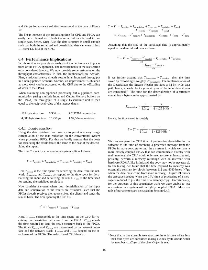
In Figure 17 we show the median values for different number of
in-flight frames both for FPGA and System B. As it can be seen
that starting with an initial overhead, the round trip times scale
linearly with respect to the number of in-flight frames. This means
that sending more than one frame in short succession increases
throughput. This is to be expected since both System A and Sys-
tem B use asynchronous I/O. Thus, when sending multiple frames
the system pays a certain constant startup cost to do things like
perhaps perform a context switch or begin the interrupt service
routine, but then can devote itself to handling the requests entire-
ly. The slope of the curve for minimum-sized frames sent to the
FPGA is 6.6 µs/in-flight frame and 10.0 µs/in-flight frame for
maximum sized frames (least squares).
Figure 16: Cumulative Histogram between System A and
FPGA for multiple outstanding transmissions (64 byte Ether-
net frames)
Figure 17: Median Round Trip Time for different number of
in-flight frames
This testing gives us a more realistic idea of what the CPU load is
for a machine when it must handle requests from the network. In
a production system in which the FPGA can write directly into the
main memory of the host server, we expect that the FPGA would
take care of the 6.6 – 10.0 µs of processing per frame plus startup
overhead that would normally need to be taken care of by CPUs
on the server to handle each request. Notice that this contribution
only considers the cycles needed to handle the data transfer. This
0.00%
10.00%
20.00%
30.00%
40.00%
50.00%
60.00%
70.00%
80.00%
90.00%
100.00%
20 30 40 50 60 70 80 90 100
Round Trip Time [s]
1 in-flight frame 2 in-flight frames
3 in-flight frames 4 in-flight frames
5 in-flight frames 6 in-flight frames
7 in-flight frames 8 in-flight frames
0
50
100
150
200
250
1 2 3 4 5 6 7 8
Ro
un
d T
rip
Tim
e (
Me
dia
n)
[s]
Number of In-flight frames
FPGA (min. frame) FPGA (max. frame)
System B (min. frame) System B (max. frame)
14
does not yet include the time required to perform the actual seria-
lization or deserialization. This will be discussed in the next
section.
6.3 Deserialization in Hardware vs. Software In this section we evaluate the performance the Deserializer cir-
cuit and compare with a traditional software implementation on
System B. We use the same setup as in the previous experiment
(Figure 13). As explained earlier, communication is implemented
by exchanging raw Ethernet frames.
6.3.1 Workload Data Set For evaluating the performance of the Deserializer we are using
the expression tree example. In particular, we use the object struc-
ture shown in Figure 18. We scale the size of the structure by the
parameter n which corresponds to the number of Operation nodes.
Figure 18: Object Structure used in Deserialization
The number of objects hence for a given n is 2n+1. As shown in
the object layout in Figure 4 both Operation and Literal objects
occupy 16 bytes on the heap. Thus, the object structure occupies
16 2𝑛 + 1 = 32𝑛 + 16 bytes on the heap. The size of the seria-
lized representation can be computed as follows:
4 heap pointer
+ 4 #objects
+ 4 2𝑛 + 1 object types
+ 4 𝑛 + 1 Literal objects
+ 9𝑛 Operation objects
= 21𝑛 + 12 bytes
Given the constraint the of the objPtr array in the current imple-
mentation, the Deserializer can process up 256 objects. Thus, in
the evaluation we vary n in the range 𝑛 ≤ 127. For 𝑛 = 127 the
size on the heap is 4,080 bytes, the size of the serialized structure
is 2,683 bytes.
The limit of Ethernet frames to 1,486 byte requires that the seria-
lized input data is split into two Ethernet frames. For transmitting
the result data, i.e., the object structure that lands on the heap,
three Ethernet frames are used.
6.3.2 Deserialization – Results Figure 19 shows the round trip times for processing a deserializa-
tion request for object structure size in the range 112—4080
bytes. For each data point we issued 1,000,000 requests and we
measured the round trip time. In the figure, the solid lines show
the min/90% percentile and the median values of the end-to-end
times both for the FPGA Deserializer and the software solution
implemented on System B.
Figure 19: Round Trip Times of FPGA Deserializer vs.
Software Solution
Figure 20: Speedup of FPGA Deserializer based on median
times
In Figure 19 it can be seen that not only the median but also the
entire min to 90%-percentile band of the FPGA implementation is
always below the software solution. The dashed lines in the figure
show the time spent for the actual processing (excluding commu-
nication cost). The slopes are increasing linearly and diverging,
hence, resulting in a constant speed up of the hardware solution as
shown in Figure 20. The computation-only speed up is approx-
imately factor 9×. The speedup is reduced to 2.5× when also
considering communication cost. A quick sanity check confirms
the measurements: The request and response can be related to the
3 in-flight messages from Section 6.2.8 which required a round
trip time of 115 µs for the FPGA and 158 µs for System B. Add-
ing the computation time of 10 µs and 96 µs respectively, the
resulting estimated total time of 125 µs for the FPGA Deserializer
+
+
+
+
+
1
2
3
n-1
n n+1
0.00
50.00
100.00
150.00
200.00
250.00
300.00
0 500 1000 1500 2000 2500 3000 3500 4000
Ro
un
d T
rip
Tim
e [
s]
Size of object structure on heap [bytes]
CPU 90% percentile CPU mediancomputing only min CPU minFPGA min FPGA medianFPGA computing only min FPGA 90% percentile
0123456789
10
0 500 1000 1500 2000 2500 3000 3500 4000
Size of object structure on heap [bytes]
Overall SpeedupComputation-only Speedup
15
and 254 µs for software solution correspond to the data in Figure
19.
The linear increase of the processing time for CPU and FPGA can
easily be explained as in both the serialized data is read in one
single pass, hence, O(n). Also the data structure is small enough
such that both the serialized and deserialized data can even fit into
L1 cache (32 kB) of the CPU.
6.4 Performance Implications In this section we provide an analysis of the performance implica-
tions of the FPGA approach. The measurements in the last section
only considered latency. We now provide some estimates on the
throughput characteristics. In fact, the implications are twofold.
First, a reduced latency directly results in an increased throughput
in a non-pipelined scenario. Second, an improvement is obtained
as more work can be processed on the CPU due to the offloading
of work to the FPGA.
When assuming non-pipelined processing but a pipelined com-
munication (using multiple Input and Output Memory buffers on
the FPGA) the throughput of a single Deserializer unit is then
equal to the reciprocal value of the latency that is:
112 byte structure: 0.336 µs 2.977M requests/sec
4,080 byte structure: 10.256 µs 97,504 requests/sec
6.4.1 Load-reduction Using the data obtained, we now try to provide a very rough
extrapolation of the load reduction on the conventional system
when processing RPCs. For this we boldly assume that the costs
for serializing the result data is the same as the cost of the deseria-
lizing the input.
The time T spent by a conventional system split as follows:
𝑇 = 𝑇receive + 𝑇deserialize + 𝑇execute + 𝑇serialize + 𝑇send
Here Treceive is the time spent for receiving the data from the net-
work, Tdeserialize and Tserialize correspond to the time spent for dese-
rializing the input and serializing the result. Tsend is the time used
for sending the serialized result data.
Now consider a system where both deserialization of the input
data and serialization of the results are offloaded, such that the
FPGA directly receives the requests from the clients and sends the
results back. The time spent by the CPU is:
𝑇 ′ = 𝑇′receive + 𝑇execute + 𝑇′send
Here, T’receive corresponds to the time spend on the CPU for re-
ceiving the deserialized structure from the FPGA. T’rsend equals
the time required to send the result structure back to the FPGA.
The times Treceive and Treceive are determined by the network inter-
face and the network stack. T’receive and T’send depend on the at-
tachment of the FPGA. The reduction of CPU time is:
𝑇 − 𝑇 ′ = 𝑇receive + 𝑇deserialize + 𝑇execute + 𝑇serialize + 𝑇send
− 𝑇 ′receive − 𝑇execute − 𝑇 ′
send
= 𝑇receive − 𝑇 ′receive + 𝑇deserialize + 𝑇serialize + 𝑇send − 𝑇 ′
send
Assuming that the size of the serialized data is approximately
equal to the deserialized data we have
𝑇 − 𝑇 ′ = 𝑇receive − 𝑇 ′receive
≈0
+ 𝑇deserialize + 𝑇serialize
+ 𝑇send − 𝑇 ′send
≈0
.
If we further assume that 𝑇deserialize ≈ 𝑇serialize, then the time
saved by offloading is roughly 2𝑇deserialize. The implementation of
the Deserializer the Stream Reader provides a 32-bit wide data
path, hence, at each clock cycles 4 bytes of the input data stream
are consumed.2 The time for the deserialization of a structure
containing n bytes can be approximated by
𝑇deserialize ≈𝑛
4𝑓clock=
𝑛
4 ∙ 125 MHz .
Hence, the time saved is roughly
𝑇 − 𝑇′ ≈𝑛
2𝑓clock=
𝑛
2 ∙ 125 MHz .
We can compare the CPU time of performing deserialization in
software to the time of receiving a processed message from the
FPGA in more concrete terms. In a system in which we have a
more closely-coupled FPGA that can communicate directly with
main memory, the CPU would only need to take an interrupt and,
possibly, perform a memcpy (although with an interface with
hardware RDMA like Infiniband, the copy may not be necessary).
In our testing, we found that the time required by memcpy was
essentially constant for blocks between 112 and 4080 bytes (~7µs
when the data must come from main memory). Figure 21 shows
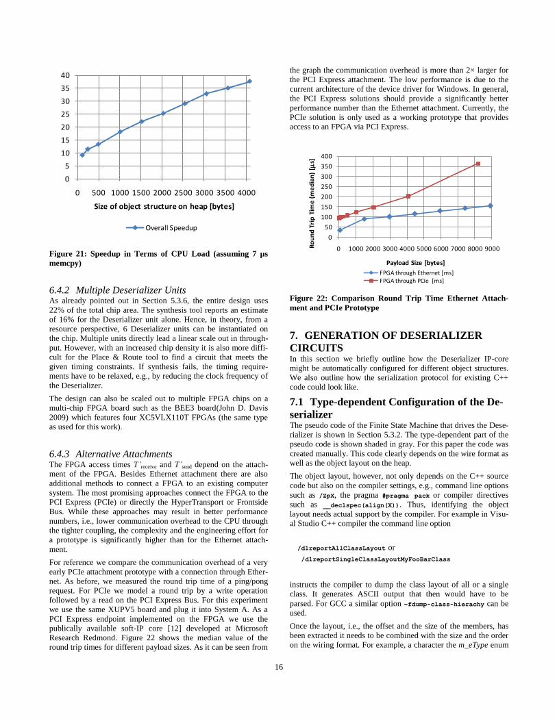
the effective speedup when the CPU time of processing of a mes-
sage is reduced to just the time of a memory copy. Unfortunately,
for the purposes of this speculative work we were unable to test
our system on a system with a tightly coupled FPGA. More de-
tails of our attempts are discussed in Section 6.4.3.
2 Note that in our example tree structure the only case where less
than four bytes are consumed during a clock cycle occurs when
the member m_eType of the class Object is read.
16
Figure 21: Speedup in Terms of CPU Load (assuming 7 µs
memcpy)
6.4.2 Multiple Deserializer Units As already pointed out in Section 5.3.6, the entire design uses
22% of the total chip area. The synthesis tool reports an estimate
of 16% for the Deserializer unit alone. Hence, in theory, from a
resource perspective, 6 Deserializer units can be instantiated on
the chip. Multiple units directly lead a linear scale out in through-
put. However, with an increased chip density it is also more diffi-
cult for the Place & Route tool to find a circuit that meets the
given timing constraints. If synthesis fails, the timing require-
ments have to be relaxed, e.g., by reducing the clock frequency of
the Deserializer.
The design can also be scaled out to multiple FPGA chips on a
multi-chip FPGA board such as the BEE3 board(John D. Davis
2009) which features four XC5VLX110T FPGAs (the same type
as used for this work).
6.4.3 Alternative Attachments The FPGA access times T’receive and T’send depend on the attach-
ment of the FPGA. Besides Ethernet attachment there are also
additional methods to connect a FPGA to an existing computer
system. The most promising approaches connect the FPGA to the
PCI Express (PCIe) or directly the HyperTransport or Frontside
Bus. While these approaches may result in better performance
numbers, i.e., lower communication overhead to the CPU through
the tighter coupling, the complexity and the engineering effort for
a prototype is significantly higher than for the Ethernet attach-
ment.
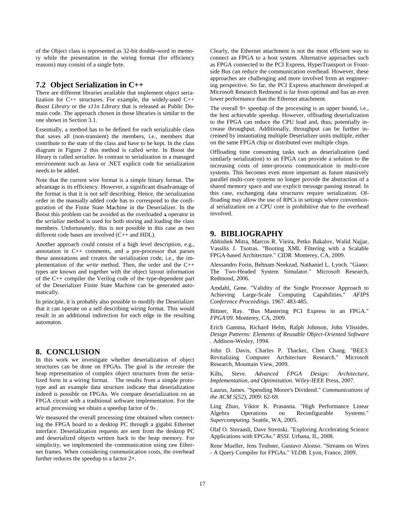
For reference we compare the communication overhead of a very
early PCIe attachment prototype with a connection through Ether-
net. As before, we measured the round trip time of a ping/pong
request. For PCIe we model a round trip by a write operation
followed by a read on the PCI Express Bus. For this experiment
we use the same XUPV5 board and plug it into System A. As a
PCI Express endpoint implemented on the FPGA we use the
publically available soft-IP core [12] developed at Microsoft
Research Redmond. Figure 22 shows the median value of the
round trip times for different payload sizes. As it can be seen from
the graph the communication overhead is more than 2× larger for
the PCI Express attachment. The low performance is due to the
current architecture of the device driver for Windows. In general,
the PCI Express solutions should provide a significantly better
performance number than the Ethernet attachment. Currently, the
PCIe solution is only used as a working prototype that provides
access to an FPGA via PCI Express.
Figure 22: Comparison Round Trip Time Ethernet Attach-
ment and PCIe Prototype
7. GENERATION OF DESERIALIZER
CIRCUITS In this section we briefly outline how the Deserializer IP-core
might be automatically configured for different object structures.
We also outline how the serialization protocol for existing C++
code could look like.
7.1 Type-dependent Configuration of the De-
serializer The pseudo code of the Finite State Machine that drives the Dese-
rializer is shown in Section 5.3.2. The type-dependent part of the
pseudo code is shown shaded in gray. For this paper the code was
created manually. This code clearly depends on the wire format as
well as the object layout on the heap.
The object layout, however, not only depends on the C++ source
code but also on the compiler settings, e.g., command line options
such as /ZpX, the pragma #pragma pack or compiler directives
such as __declspec(align(X)). Thus, identifying the object
layout needs actual support by the compiler. For example in Visu-
al Studio C++ compiler the command line option
/d1reportAllClassLayout or
/d1reportSingleClassLayoutMyFooBarClass
instructs the compiler to dump the class layout of all or a single
class. It generates ASCII output that then would have to be
parsed. For GCC a similar option –fdump-class-hierachy can be
used.
Once the layout, i.e., the offset and the size of the members, has
been extracted it needs to be combined with the size and the order
on the wiring format. For example, a character the m_eType enum
0
5
10
15
20
25
30
35
40
0 500 1000 1500 2000 2500 3000 3500 4000
Size of object structure on heap [bytes]
Overall Speedup0
50
100
150
200
250
300
350
400
0 1000 2000 3000 4000 5000 6000 7000 8000 9000Ro
un
d T
rip
Tim
e (
me
dia
n)
[s]
Payload Size [bytes]
FPGA through Ethernet [ms]FPGA through PCIe [ms]
17
of the Object class is represented as 32-bit double-word in memo-
ry while the presentation in the wiring format (for efficiency
reasons) may consist of a single byte.
7.2 Object Serialization in C++ There are different libraries available that implement object seria-
lization for C++ structures. For example, the widely-used C++
Boost Library or the s11n Library that is released as Public Do-
main code. The approach chosen in those libraries is similar to the
one shown in Section 3.1.
Essentially, a method has to be defined for each serializable class
that saves all (non-transient) the members, i.e., members that
contribute to the state of the class and have to be kept. In the class
diagram in Figure 2 this method is called write. In Boost the
library is called serialize. In contrast to serialization in a managed
environment such as Java or .NET explicit code for serialization
needs to be added.
Note that the current wire format is a simple binary format. The
advantage is its efficiency. However, a significant disadvantage of
the format is that it is not self describing. Hence, the serialization
order in the manually added code has to correspond to the confi-
guration of the Finite State Machine in the Deserializer. In the
Boost this problem can be avoided as the overloaded & operator in
the serialize method is used for both storing and loading the class
members. Unfortunately, this is not possible in this case as two
different code bases are involved (C++ and HDL).
Another approach could consist of a high level description, e.g.,
annotation in C++ comments, and a pre-processor that parses
these annotations and creates the serialization code, i.e., the im-
plementation of the write method. Then, the order and the C++
types are known and together with the object layout information
of the C++ compiler the Verilog code of the type-dependent part
of the Deserializer Finite State Machine can be generated auto-
matically.
In principle, it is probably also possible to modify the Deserializer
that it can operate on a self describing wiring format. This would
result in an additional indirection for each edge in the resulting
automaton.
8. CONCLUSION In this work we investigate whether deserialization of object
structures can be done on FPGAs. The goal is the recreate the
heap representation of complex object structures from the seria-
lized form in a wiring format. The results from a simple proto-
type and an example data structure indicate that deserialization
indeed is possible on FPGAs. We compare deserialization on an
FPGA circuit with a traditional software implementation. For the
actual processing we obtain a speedup factor of 9.
We measured the overall processing time obtained when connect-
ing the FPGA board to a desktop PC through a gigabit Ethernet
interface. Deserialization requests are sent from the desktop PC
and deserialized objects written back to the heap memory. For
simplicity, we implemented the communication using raw Ether-
net frames. When considering communication costs, the overhead
further reduces the speedup to a factor 2×.
Clearly, the Ethernet attachment is not the most efficient way to
connect an FPGA to a host system. Alternative approaches such
as FPGA connected to the PCI Express, HyperTransport or Front-
side Bus can reduce the communication overhead. However, these
approaches are challenging and more involved from an engineer-
ing perspective. So far, the PCI Express attachment developed at
Microsoft Research Redmond is far from optimal and has an even
lower performance than the Ethernet attachment.
The overall 9× speedup of the processing is an upper bound, i.e.,
the best achievable speedup. However, offloading deserialization
to the FPGA can reduce the CPU load and, thus, potentially in-
crease throughput. Additionally, throughput can be further in-
creased by instantiating multiple Deserializer units multiple, either
on the same FPGA chip or distributed over multiple chips.
Offloading time consuming tasks such as deserialization (and
similarly serialization) to an FPGA can provide a solution to the
increasing costs of inter-process communication in multi-core
systems. This becomes even more important as future massively
parallel multi-core systems no longer provide the abstraction of a
shared memory space and use explicit message passing instead. In
this case, exchanging data structures require serialization. Of-
floading may allow the use of RPCs in settings where convention-
al serialization on a CPU core is prohibitive due to the overhead
involved.
9. BIBLIOGRAPHY Abhishek Mitra, Marcos R. Vieira, Petko Bakalov, Walid Najjar,
Vassilis J. Tsotras. "Booting XML Filtering with a Scalable
FPGA-based Architecture." CIDR. Monterey, CA, 2009.
Alessandro Forin, Behnam Neekzad, Nathaniel L. Lynch. "Giano:
The Two-Headed System Simulator." Microsoft Research,
Redmond, 2006.
Amdahl, Gene. "Validity of the Single Processor Approach to
Achieving Large-Scale Computing Capabilities." AFIPS
Conference Proceedings. 1967. 483-485.
Bittner, Ray. "Bus Mastering PCI Express in an FPGA."
FPGA'09. Monterey, CA, 2009.
Erich Gamma, Richard Helm, Ralph Johnson, John Vlissides.
Design Patterns: Elements of Reusable Object-Oriented Software
. Addison-Wesley, 1994.
John D. Davis, Charles P. Thacker, Chen Chang. "BEE3:
Revitalizing Computer Architecture Research." Microsoft
Research, Mountain View, 2009.
Kilts, Steve. Advanced FPGA Design: Architecture,
Implementation, and Optimization. Wiley-IEEE Press, 2007.
Laurus, James. "Spending Moore's Dividend." Communications of
the ACM 5(52), 2009: 62-69.
Ling Zhuo, Viktor K. Prasanna. "High Performance Linear
Algebra Operations on Reconfigurable Systems."
Supercomputing. Seattle, WA, 2005.
Olaf O. Storaasli, Dave Strenski. "Exploring Accelerating Science
Applications with FPGAs." RSSI. Urbana, IL, 2008.
Rene Mueller, Jens Teubner, Gustavo Alonso. "Streams on Wires
- A Query Compiler for FPGAs." VLDB. Lyon, France, 2009.
18
Tim Oliver, Bertil Schmidt, Douglas Maskel. "Hyper Customized
Processor for Bio-Sequence Database Scanning on FPGAs."
FPGA. Monterey, CA, 2005.
Tom van Court, Yongfeng Gu, Martin C. Herbordt. "FPGA
Acceleration of Rigit Molecule Interactions." FCCM. Napa, CA,
2004.
Tukey, John Wilder. Exploratory Data Analysis. Addison-Wesley,
1977.


![Json Deserialization Exploitation - OWASP3 I OWASP Stammtisch Dresden - JSON Deserialization I 10.08.2018 Introduction DefCon 2017: “Friday the 13th: JSON Attacks” [1] Slides quite](https://img.pdfslide.us/doc/110x75/5f02cc227e708231d4060f2e/json-deserialization-exploitation-owasp-3-i-owasp-stammtisch-dresden-json-deserialization.jpg)