Embed Size (px)
Citation preview
HELIOS D010 – State of the art on Photonics on CMOS
Page 1 of 102
FP7 - 224312 HELIOS
pHotonics ELectronics functional Integration on CMOS
D010 – State of the art on Photonics on CMOS, 3rd update
Due date of deliverable: 30/10/2011 (M42) Actual submission date: 24/01/2012
Start date of project: 01/05/2008 (M01) Duration: 48 months
Lead contractor for this deliverable Name: CEA-LETI
Contact Person: Jean-Marc FEDELI Address: 17, rue des Martyrs. 38054 GRENOBLE Cedex 9
Phone: +33 4 38 78 68 79 E-mail: [email protected]
Authors:, Delphine Marris-Morini, , Laurent Vivien, Aleksey Anopchenko, Dave Thomson, Henri Porte, Dries Van Thourhout, Shahram Keyvaninia, Lars Zimmerman, Pablo Sanchis, Jose V Galan, Antoine Brimont, Guanghua Duan, Andreas Hakansson, Ian O Connor, P Viktorovitch, F. Della Corte, Wim Bogaerts, Alban Leliepvre, Clément Chauveau, Marco Lamponi, Badhise Ben Bakir, Jean-Marc Fedeli
Participants: CEA, CNRS, UNITN, UPVLC, IMEC, DAS, PHOTLINE, UNIS, TUB, III-V LAB Workpackage: WP0b
Nature: Report Security: Public Total number of pages: 102
Summary: This deliverable gives an overview of the recent achievements on silicon photonics devices related to the objectives of the HELIOS project. So, the focus is given on heterogeneous source, modulators, photodetectors, passives for communication applications, silicon photonics packaging, transceivers, and integration with electronic technologies. Keyword list: Light sources, modulators, photodetectors, mux, demux, couplers, transceivers
HELIOS D010 – State of the art on Photonics on CMOS
Page 2 of 102
Table of Contents
1- Introduction .......................................................................................................... 4
2- Sources ................................................................................................................. 4 2.1- InP laser bonded on Si............................................................................................................. 4
2.1.1- Integration routes........................................................................................................... 4 2.1.2- Electrically pumped III-V lasers on Silicon .................................................................... 5 2.1.3- Conclusion on III-V lasers on silicon ........................................................................... 14
2.2- Silicon and Germanium sources ............................................................................................ 14 2.3- 2.5D sources .......................................................................................................................... 20
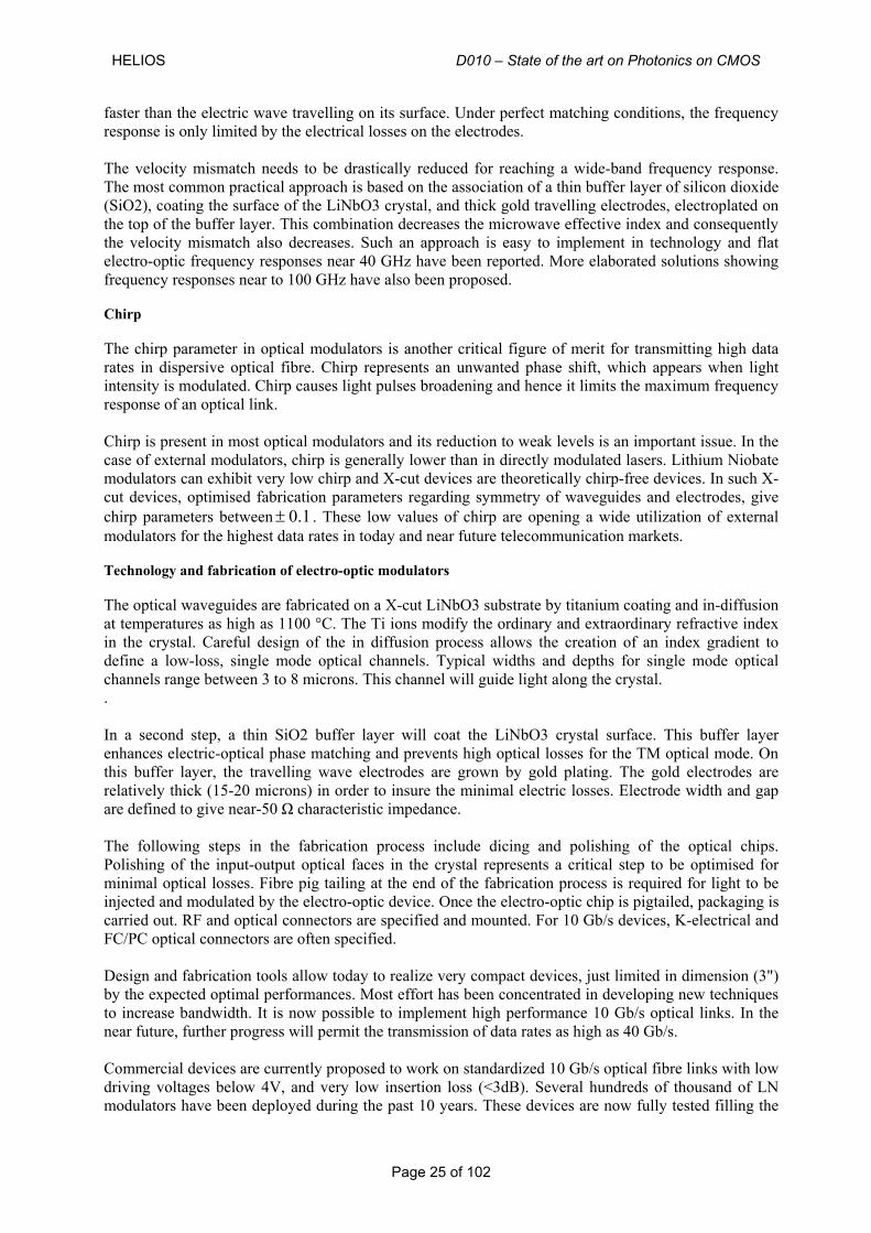
3- Modulators .......................................................................................................... 21 3.1- Packaged modulator on the market ....................................................................................... 21
3.1.1- High speed semiconductor MZI modulators................................................................ 21 3.1.2- Lithium Niobate Electro-optic Modulators ................................................................... 23
3.2- Overview on modulators on silicon ........................................................................................ 26 3.3- Cristalline silicon modulators ................................................................................................. 27 3.4- SiGe Modulators .................................................................................................................... 47 3.5- InP bonded modulator............................................................................................................ 52 3.6- Amorphous Si modulator........................................................................................................ 54
4- Photodiodes on Si.............................................................................................. 55 4.1- Photodiodes Ge on Si ............................................................................................................ 55 4.2- Avalanche germanium photodiodes....................................................................................... 57 4.3- InGaAs PD bonded on Si ....................................................................................................... 58
5- MUX-DEMUX ....................................................................................................... 62 5.1- Introduction ............................................................................................................................ 62 5.2- AWG type............................................................................................................................... 62 5.3- MZI based .............................................................................................................................. 64 5.4- ECHELLE type ....................................................................................................................... 65 5.5- Ring resonator based devices ............................................................................................... 66
6- Silicon Photonics Packaging ............................................................................ 70 6.1- Optical fibers couplers............................................................................................................ 70
6.1.1- Three dimensional adiabatic tapers ............................................................................ 71 6.1.2- Anti-resonant reflecting optical waveguides................................................................ 71 6.1.3- Adiabatic inverse tapers .............................................................................................. 72 6.1.4- Polarization management with inverted tapers (Badhise)........................................... 74 6.1.5- Grating couplers .......................................................................................................... 76 6.1.6- Fiber coupling structures comparison ......................................................................... 79
6.2- Fiber pigtailing........................................................................................................................ 80 6.3- Advanced Packaging architecture ......................................................................................... 84
7- Design flow integration for photonics.............................................................. 86
8- Convergence Photonics- Electronics............................................................... 87 8.1- LUXTERA............................................................................................................................... 88 8.2- MIT&BAE ............................................................................................................................... 91
HELIOS D010 – State of the art on Photonics on CMOS
Page 3 of 102
8.3- IBM......................................................................................................................................... 91 8.4- INTEL ..................................................................................................................................... 92 8.5- SELETE (Japan) .................................................................................................................... 92 8.6- ORACLE................................................................................................................................. 93 8.7- LETI & IMEC .......................................................................................................................... 94
9- 16x10 Gbit/s transceiver .................................................................................... 94 9.1- Monolithic PICs on InP (Infinera) ........................................................................................... 95 9.2- Luxtera active cable chip........................................................................................................ 96 9.3- INTEL PICs with InP on SOI lasers ....................................................................................... 97
10- Wireless transmission systems................................................................ 99 10.1- Millimeter wave wireless transmission ................................................................................... 99 10.2- Photonics wireless transmission systems............................................................................ 101
11- List of abbreviations.................................................................................102
HELIOS D010 – State of the art on Photonics on CMOS
Page 4 of 102
1- Introduction
This D010 HELIOS project deliverable gives an overview of the recent achievements on silicon photonics devices related to the objectives of the HELIOS project. So, the focus is given on heterogeneous sources, modulators, photodetectors, passives for communication applications, silicon photonics packaging, transceivers, and integration with electronic technologies. This report is not intended to be exhaustive, but preferably an easy to read and up to date document. More specific information will be found in the references. Comments and maybe claims can be addressed to [email protected] .
2- Sources
Photonic integrated circuits offer the potential of realizing low-cost and compact optical
functions. Silicon-on-insulator (SOI) is a promising material platform for this photonic integration, as one can rely on the massive electronics processing infrastructure to process the optical components. However, the integration of a Si laser is hampered by its indirect bandgap. In this project, it is proposed to integrate a direct bandgap III-V layer on top of a SOI waveguide substrate to achieve stimulated light emission and to couple this stimulated emission to the underlying SOI waveguide circuit as a short term development. As an alternative route, Si based sources are also studied.
2.1- InP laser bonded on Si
2.1.1- Integration routes
Three main methods have been explored to integrate III-V material on silicon. The first one is the
flip-chip technology. Its principle relies on the bonding of individual laser dies to a silicon-on-insulator (SOI) substrate by the means of metal bumps. The main challenge when flip-chipping optoelectronic dies is the strict alignment tolerance (< 1 μm) that arises when coupling light from the active component into a fibre or on-chip waveguide. While flip-chip is the most mature technology, the slowness of the process and the low integration density that it enables both lead to high fabrication costs.
The second approach is the monolithic integration of III-V materials by hetero-epitaxial growth on a silicon substrate1. Even though this technique could lead to highly integrated devices, large dislocation densities that degrade the optical properties of the devices are a major problem to overcome.
The last technique is the heterogeneous integration of III-V materials by wafer bonding. The idea is to transfer a III-V stack from its original growth substrate to a SOI wafer by the means of bonding. The III-V laser diodes are next fabricated on their SOI wafer using wafer-scale processing. This technique allows a high density of integration, collective processing and the use of high-quality III-V layers. The light can be directly coupled into a silicon waveguide which is included in the SOI underneath the epitaxy.
The III-V stack can be bonded to a SOI wafer either wafer-to-wafer or die-to-wafer. The advantage of die-to-wafer bonding is that it reduces the cost of the integration process since expensive III-V stacks can be bonded only where they are needed.
Three types of bonding are used in the literature: Molecular bonding, adhesive bonding and metal bonding. Direct bonding takes advantage of Van Der Waals interactions between two oxidized and hydrophilic surfaces. As it requires a very intimate contact between the surfaces, the bonding quality is
1 J. Yang, P. Bhattacharya, G. Qin, Z. Ma, "On-Chip Integration of InGaAs/GaAs Quantum dot lasers with waveguides and modulators on silicon," Proc. SPIE Vol. 6909 (2008).
HELIOS D010 – State of the art on Photonics on CMOS
Page 5 of 102
very sensitive to the surface roughness and particles2. The thickness of the bonding layer is characterised by the oxide thickness left between the III-V and the silicon layers. It varies depending on the technological process developed by the different research teams.
Adhesive bonding uses the thermosetting polymer divinylsiloxane benzocyclobutene (DVS-BCB) as a bonding agent. DVS-BCB compensates for the surface roughness, therefore the bonding tolerances are more relaxed compared to molecular bonding. However, DVS-BCB has a lower thermal conductance than SiO2. Self-heating might prevent continuous-wave (CW) lasing3, nevertheless this problem can be circumvented by using a metallic via upon the laser that extracts heat out of the device2.
Metal bonding combines the advantages of low bonding temperature, high thermal conduction, no critical cleanliness requirements and a potentially ohmic electrical interface. Because of strong light absorption, the bonding metals are required to be far away from the light propagation area4.
2.1.2- Electrically pumped III-V lasers on Silicon
The first demonstrations of electrically pumped lasers bonded on silicon have been done by Wada
and Kamijoh5 in 1996. A Fabry-Perot laser was fabricated in an InP film bonded on silicon by molecular wafer bonding. Continuous-wave lasing was obtained at room-temperature. A threshold current of 50 mA and a maximum output power of 7 mW were reported. Other demonstrations came ten years later, thanks to the maturation of silicon photonics, particularly through the work of European research teams linked by projects like PICMOS (IMEC, CEA-LETI, INL) supported by the European community, and American teams (UCSB, CALTECH, Intel) supported by grants from Intel Corp. and from the Defence Advanced Research Projects Agency (DARPA).
Several types of lasers on silicon have been demonstrated so far, including microdisks, Fabry-Perot lasers, racetrack resonator lasers, distributed feedback (DFB) lasers and distributed Bragg reflector (DBR) lasers.
Microdisk lasers and hybrid microring lasers
Microdisk lasers have shown great potential for applications such as intra-chip optical
interconnects, thanks to their low-power consumption and small footprint. Micron-sized, electrically injected microdisks have been demonstrated6,7,8,9. A schematic
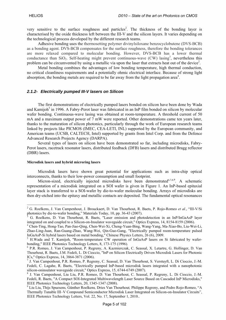
representation of a microdisk integrated on a SOI wafer is given in Figure 1. An InP-based epitaxial layer stack is transferred to a SOI-wafer by die-to-wafer molecular bonding. Arrays of microdisks are then dry-etched into the epitaxy and metallic contacts are deposited. The fundamental optical resonances
2 G. Roelkens, J. Van Campenhout, J. Brouckaert, D. Van Thourhout, R. Baets, P. Rojo-Romeo et al., “III-V/Si photonics by die-to-wafer bonding,” Materials Today, 10, pp. 36-43 (2007). 3 G. Roelkens, D. Van Thourhout, R. Baets, "Laser emission and photodetection in an InP/InGaAsP layer integrated on and coupled to a Silicon-on-Insulator waveguide circuit," Optics Express, 14, 8154-8159 (2006). 4 Chen-Ting, Hong-Tao, Pan-Jiao-Qing, Chen-Wei-Xi, Cheng-Yuan-Bing, Wang-Yang, Ma-Xiao-Bo, Liu-Wei-Li, Zhao-Ling-Juan, Ran-Guang-Zhao, Wang-Wei, Qin-Guo-Gang, "Electrically pumped room-temperature pulsed InGaAsP-Si hybrid lasers based on metal bonding," Chinese Physics Letters, 26 (6), 2009. 5 H.Wada and T. Kamijoh, "Room-temperature CW operation of InGaAsP lasers on Si fabricated by wafer-bonding," IEEE Photonics Technology Letters, 8, 173-175 (1996). 6 P.R. Romeo, J. Van Campenhout, P. Regreny, A. Kazmierczak, C. Seassal, X. Letartre, G. Hollinger, D. Van Thourhout, R. Baets, J.M. Fedeli, L. Di Cioccio, "InP on Silicon Electrically Driven Microdisk Lasers for Photonic ICs," Optics Express, 14, 3864-3871 (2006). 7 J. Van Campenhout, P.R. Romeo, P. Regreny, C. Seassal, D. Van Thourhout, S. Verstuyft, L. Di Cioccio, J.-M. Fedeli, C. Lagahe, R. Baets, "Electrically pumped InP-based microdisk lasers integrated with a nanophotonic silicon-oninsulator waveguide circuit," Optics Express, 15, 6744-6749 (2007). 8 J. Van Campenhout, Liu Liu, P.R. Romeo, D. Van Thourhout, C. Seassal, P. Regreny, L. Di Cioccio, J.-M. Fedeli, R. Baets, "A Compact SOI-Integrated Multiwavelength Laser Source Based on Cascaded InP Microdisks," IEEE Photonics Technology Letters, 20, 1345-1347 (2008). 9 Liu Liu, Thijs Spuesens, Günther Roelkens, Dries Van Thourhout, Philippe Regreny, and Pedro Rojo-Romeo, “A Thermally Tunable III–V Compound Semiconductor Microdisk Laser Integrated on Silicon-on-Insulator Circuits”, IEEE Photonics Technology Letters, Vol. 22, No. 17, September 1, 2010..
HELIOS D010 – State of the art on Photonics on CMOS
Page 6 of 102
in such a structure are whispering gallery modes which are confined to the edges of the microdisk. Light coupling to a silicon waveguides is achieved by evanescent coupling on a wire waveguide (220 nm x 500 nm). So as to avoid huge losses due to internal absorption by a heavily doped p-type contact layer, a tunnel junction in combination with another n-type contact is implemented. Fabrication on a 200mm microelectronics fabrication line has been recently achieved by LETI. With the same bonded epitaxial layer, InP µsources (ring or disks) were obtained with InGaAs photodetectors.10
By integrating four microdisks of different diameters on a single waveguide, a multi-wavelength laser was also obtained7. Indeed, microdisk lasers can yield single wavelength output and their wavelength selection is determined by the round trip cavity length. The multi-wavelength output spectrum contained four laser peaks, uniformly distributed by design within the free-spectral range of a single microdisk. At equal drive currents, the peak power of the channels varied up to 8 dB, due to loss caused by parasitic coupling to the higher order modes of the neighbouring microdisks.
Figure 1. Layout of a single SOI-integrated microdisk laser8.
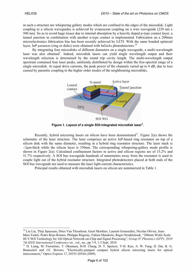
Recently, hybrid microring lasers on silicon have been demonstrated11. Figure 2(a) shows the schematic of the laser structure. The laser comprises an active InP-based ring resonator on top of a silicon disk with the same diameter, resulting in a hybrid ring resonator structure. The laser stack is ~2μm-thick while the silicon layer is 350nm. The corresponding whispering-gallery mode profile is shown in Figure 2(a). Calculated confinement factors in active and silicon regions are of 15.2% and 51.7% respectively. A SOI bus waveguide hundreds of nanometers away from the resonator is used to couple light out of the hybrid resonator structure. Integrated photodetectors placed at both ends of the SOI bus waveguide are used to measure the laser light-current characteristics.
Principal results obtained with microdisk lasers on silicon are summarized in Table 1.
10 Liu Liu, Thijs Spuesens, Dries Van Thourhout, Geert Morthier, Laurent Grenouillet, Nicolas Olivier, Jean- Marc Fedeli, Pedro Rojo-Romeo, Philippe Régreny, Fabien Mandorlo, Regis Oroubtchouk, “200mm Wafer Scale III-V/SOI Technology for All-Optical Network-on-Chip and Signal Processing”, Group IV Photonics (GFP), 2010 7th IEEE International Conference on , vol., no., pp.7-9, 1-3 Sept. 2010 11 D. Liang, M. Fiorentino, T. Okumura, H-H. Chang, D. T. Spencer, Y-H. Kuo, A. W. Fang, D. Dai, R. G. Beausoleil and J.E. Bowers, "Electrically-pumped compact hybrid silicon microring lasers for optical interconnects," Optics Express 17, 20355-20364 (2009).
HELIOS D010 – State of the art on Photonics on CMOS
Page 7 of 102
Figure 2. (a) Schematic of hybrid ring resonator laser with BPM mode profile and integrated
photodetectors. (b) The microscopic image of a finished device with critical dimension labeled. (c) SEM cross-sectional image of the evanescent point coupler10.
Table 1 : State of the art of Microdisks lasers on silicon
Bonding type Coupling scheme Characterisation Remarks Year Ref.
Die-to-wafer molecular bonding
Evanescent on SOI channel waveguide
Pumping regime : CW λ = 1580 nm + 2nm tuning
Ith = 0.3 mA Pmax=36µW
Tunable 2010 9
Die-to-wafer molecular bonding
(thickness : 130 nm)
Evanescent on SOI channel waveguide
Pumping regime : CW λ = 1600 nm (at 1.4 mA)
Ith = 0.5 mA Jth = 1,13 kA/cm²
Pmax = 10 μW
Multimode emission 2007 7
Die-to-wafer molecular bonding
(thickness : 180 nm)
Evanescent on SOI channel waveguide
Pumping regime : CW λ = 1585 nm (at 2.8mA)
Ith = 0.9 mA Pmax = 12 μW
Four microdisks are integrated on
a single waveguide so as
to obtain a multiwavelength
transmitter
2007 8 Mic
rodi
sks
wafer-to-wafer molecular bonding
(thickness : few nanometers)
Evanescent on SOI channel waveguide
Pumping regime : CW λ = 1530 nm (at 16 mA)
Ith = 5.97 mA Pmax = 250 μW
Integrated photodetectors 2009 11
Fabry-Pérot lasers For fiber-to-the-home (FTTH) applications, high optical output power (milliwatt range) would be
required while the device footprint and the power consumption would be of minor importance. For such applications, Fabry-Perot lasers on silicon were developed.
The fabrication is made using the wafer-to-wafer or die-to-wafer bonding techniques previously cited. The definition of the facets is made either by dicing and polishing12,13,14,15,16,17, or dry-etching2, 3,18. Facet 12 A.W. Fang, H. Park, O. Cohen, R. Jones, M.J. Paniccia, J.E. Bowers "Electrically pumped hybrid AlGaInAs-silicon evanescent laser," Optics Express, 14, 9203-9210 (2006). 13 H-H. Chang, A.W. Fang, M.N. Sysak, H. Park, R. Jones, O. Cohen, O. Raday, M.J. Paniccia, J.E. Bowers, "1310nm silicon evanescent laser," Optics Express, 15, 11466-11471, (2007).
HELIOS D010 – State of the art on Photonics on CMOS
Page 8 of 102
dry-etching has the advantage of being CMOS-compatible and does not restrict the length of the silicon waveguide to the length of the laser cavity. A H+ proton implantation on both sides of the mesa can be used so as to prevent lateral current leakage11, 12, 13,14. Gold-based metallization layers made by lift-off are usually used to obtain ohmic contacts on InP. Nevertheless gold acts as a deep level in silicon and is therefore strictly forbidden in a microelectronics room. Moreover, the lift off process is not well known in the field of microelectronics where usually thin photoresist layers are used. CMOS compatible nonalloyed ohmic contacts on both n-InP and p-InGaAs III/V dice were obtained with microelectronics standard as deposited Ti/TiN/AlCu metal stacks. These developments led to the demonstration of a Fabry-Perot laser on silicon.
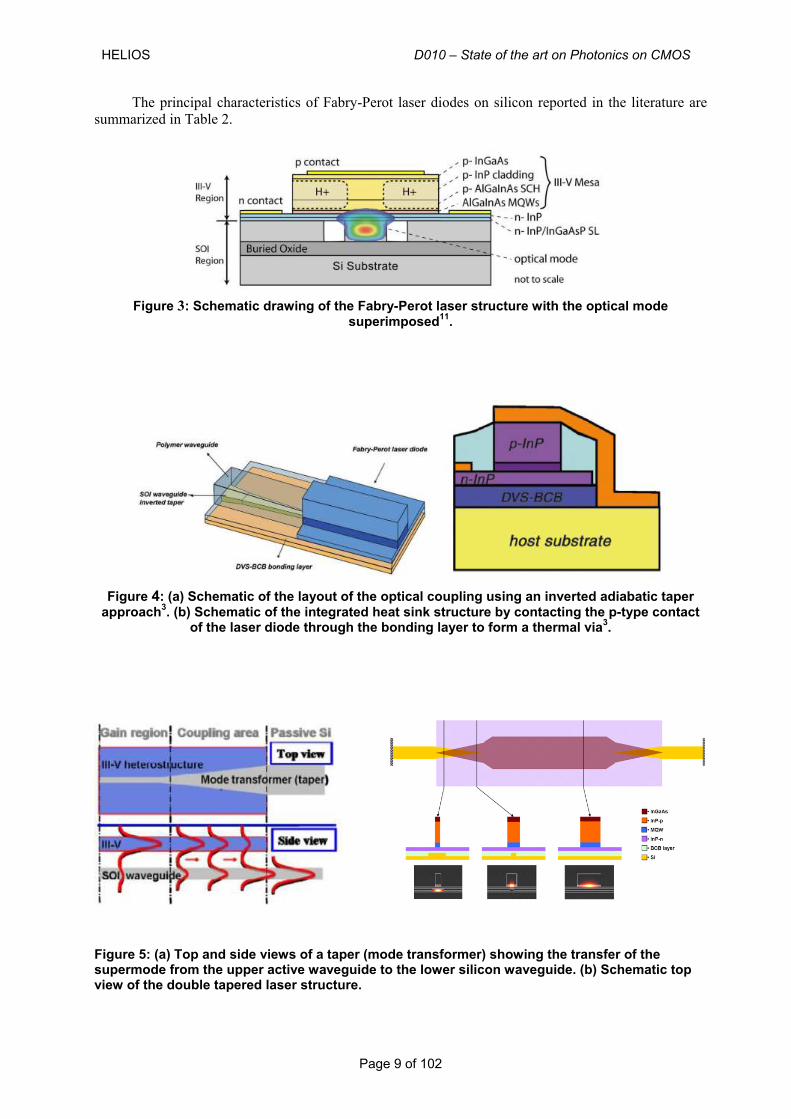
Coupling designs differ according to the bonding technology. A very thin bonding layer (< 5 nm) is particularly favourable to an evanescent coupling scheme11,12. The optical mode of these lasers overlaps both the III-V material and the silicon waveguide. Therefore the optical field can obtain gain from the III-V region while being guided by the underlying silicon waveguide region. A schematic view of this laser structure is given in Figure 3.
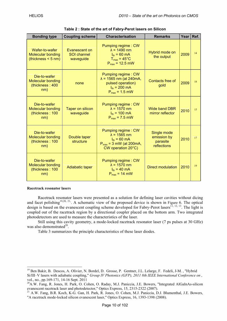
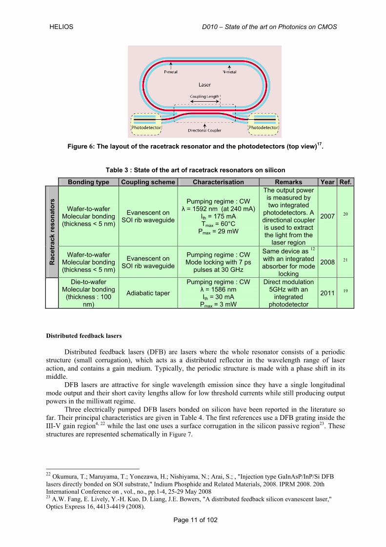
An adiabatic taper design can be chosen when the bonding interface is relatively thick2, 3,15,16 , in this case there is a complete transfer of the optical mode from the silicon waveguide to the III-V waveguide and vice versa. In such a way the optical mode experiments a high optical gain in the laser central region while maintaining a high coupling efficiency with the bottom silicon waveguide on the output part. This architecture overcomes the compromise between modal gain and coupling efficiency, inherent in the Si evanescent lasers. This results in a larger gain available for amplification and theoretically, an increased efficiency. Different approaches have been investigated. In one configuration the adiabatic taper is located into the silicon waveguide under the III-V waveguide15, as the width of the silicon is increased the optical mode is adiabatically transferred from one waveguide to the other as shown in Figure 5(a). Continuous-wave operation has been achieved with output power as high as 14 mW. In a second configuration both the III-V and the silicon waveguide are tapered to increase the coupling efficiency (Figure 5 (b))16. Continuous-wave laser action with 3mW output power inside the silicon waveguide has been achieved. In another configuration the laser diode is butt-coupled to a polymer waveguide after which the optical mode is gradually transformed into that of the SOI waveguide by increasing the cross-sectional area of the Si wire. This coupling layout is represented schematically in Figure 4(a). In these devices, no continuous-wave operation has been achieved. This behaviour is related to the high thermal resistance of the bonded laser diodes, arising from the low thermal conductivity of the bonding layer (both DVS-BCB and SiO2) and the presence of the 1 μm thick buried oxide layer on the SOI waveguide substrate. As the thickness of the buried oxide layer in this case cannot be reduced to prevent the leakage of light from the 220 nm thick Si wire to the Si substrate, and as the thickness of the bonding layer is determined by the design of the laser cavity, an additional heat sink structure has to be incorporated to reduce the thermal resistance of the bonded device. This can be achieved by using the top-contact of the laser diode as a thermal via to sink the heat generated in the laser structure through the bonding layer, as shown schematically in Figure 4 (b).
By incorporating an absorbing region in front of the lasing output, Fabry-Perot mode-locked lasers on silicon were also demonstrated13. A repetition frequency of up to 40 GHz has been reported. 14 B.R. Koch, A.W. Fang, O. Cohen, and J.E. Bowers, "Mode-locked silicon evanescent lasers," Optics express, 15, 11225-11233 (2007). 15 Sun, Xiankai; Shearn, Michael J.; Zadok, Avi; Leite, Marina S.; Steger, Scott T.; Atwater, Harry A.; Scherer, Axel; Yariv, Amnon; , "Electrically pumped supermode Si/InGaAsP hybrid lasers," Lasers and Electro-Optics (CLEO) and Quantum Electronics and Laser Science Conference (QELS), 2010 Conference on , vol., no., pp.1-2, 16-21 May 2010 16 B. Ben Bakir, N. Olivier, Ph. Grosse, S. Messaoudène, S. Brision, E. Augendre, P. Philippe, K. Gilbert, D. Bordel, J. Harduin and J.-M. Fedeli, "Electrically driven hybrid Si/III-V lasers based on adiabatic mode transformers", Proc. SPIE 7719, 77191F (2010) 17 Lamponi, M.; Keyvaninia, S.; Pommereau, F.; Brenot, R.; de Valicourt, G.; Lelarge, F.; Roelkens, G.; Van Thourhout, D.; Messaoudene, S.; Fedeli, J.-M.; Duan, G.-H.; , "Heterogeneously integrated InP/SOI laser using double tapered single-mode waveguides through adhesive die to wafer bonding," Group IV Photonics (GFP), 2010 7th IEEE International Conference on , vol., no., pp.22-24, 1-3 Sept. 2010 18 Grenouillet, L.; Bavencove, A.L.; Dupont, T.; Harduin, J.; Philippe, P.; Regreny, P.; Lelarge, F.; Gilbert, K.; Grosse, P.; Fedeli, J.M.; , "CMOS compatible contacts and etching for InP-on-silicon active devices," Group IV Photonics, 2009. GFP '09. 6th IEEE International Conference on , vol., no., pp.196-198, 9-11 Sept. 2009
HELIOS D010 – State of the art on Photonics on CMOS
Page 9 of 102
The principal characteristics of Fabry-Perot laser diodes on silicon reported in the literature are summarized in Table 2.
Figure 3: Schematic drawing of the Fabry-Perot laser structure with the optical mode
superimposed11.
Figure 4: (a) Schematic of the layout of the optical coupling using an inverted adiabatic taper
approach3. (b) Schematic of the integrated heat sink structure by contacting the p-type contact of the laser diode through the bonding layer to form a thermal via3.
Figure 5: (a) Top and side views of a taper (mode transformer) showing the transfer of the supermode from the upper active waveguide to the lower silicon waveguide. (b) Schematic top view of the double tapered laser structure.
HELIOS D010 – State of the art on Photonics on CMOS
Page 10 of 102
Table 2 : State of the art of Fabry-Perot lasers on Silicon
Bonding type Coupling scheme Characterisation Remarks Year Ref.
Wafer-to-wafer Molecular bonding (thickness < 5 nm)
Evanescent on SOI channel waveguide
Pumping regime : CW λ = 1490 nm Ith = 60 mA Tmax = 45°C
Pmax = 12.5 mW
Hybrid mode on the output 2009 14
Die-to-wafer Molecular bonding
(thickness : 400 nm)
none
Pumping regime : CW λ = 1565 nm (at 240mA,
pulsed operation) Ith = 200 mA
Pmax = 1.5 mW
Contacts free of gold 2009 18
Die-to-wafer Molecular bonding
(thickness : 100 nm)
Taper on silicon waveguide
Pumping regime : CW λ = 1570 nm Ith = 100 mA
Pmax = 7.5 mW
Wide band DBR mirror reflector 2010 15
Die-to-wafer Molecular bonding
(thickness : 100 nm)
Double taper structure
Pumping regime : CW λ = 1565 nm Ith = 60 mA
Pmax = 3 mW (at 200mA, CW operation 20°C)
Single mode emission by
parasite reflections
2010 17
Die-to-wafer Molecular bonding
(thickness : 100 nm)
Adiabatic taper
Pumping regime : CW λ = 1570 nm Ith = 40 mA
Pmax = 14 mW
Direct modulation 2010 19
Racetrack resonator lasers
Racetrack resonator lasers were presented as a solution for defining laser cavities without dicing
and facet polishing19,20, 21,. A schematic view of the proposed device is shown in Figure 6. The optical design is based on the evanescent coupling scheme developed for Fabry-Perot lasers11, 12, 13. The light is coupled out of the racetrack region by a directional coupler placed on the bottom arm. Two integrated photodetectors are used to measure the characteristics of the laser.
Still using this cavity geometry, a mode-locked racetrack resonator laser (7 ps pulses at 30 GHz) was also demonstrated20.
Table 3 summarizes the principle characteristics of these laser diodes.
19 Ben Bakir, B. Descos, A. Olivier, N. Bordel, D. Grosse, P. Gentner, J.L. Lelarge, F. Fedeli, J-M. , "Hybrid Si/III–V lasers with adiabatic coupling," Group IV Photonics (GFP), 2011 8th IEEE International Conference on , vol., no., pp.169-171, 14-16 Sept. 2011 20A.W. Fang, R. Jones, H. Park, O. Cohen, O. Raday, M.J. Paniccia, J.E. Bowers, "Integrated AlGaInAs-silicon evanescent racetrack laser and photodetector," Optics Express, 15, 2315-2322 (2007). 21 A.W. Fang, B.R. Koch, K-G. Gan, H. Park, R. Jones, O. Cohen, M.J. Paniccia, D.J. Blumenthal, J.E. Bowers, "A racetrack mode-locked silicon evanescent laser," Optics Express, 16, 1393-1398 (2008).
HELIOS D010 – State of the art on Photonics on CMOS
Page 11 of 102
Figure 6: The layout of the racetrack resonator and the photodetectors (top view)17.
Table 3 : State of the art of racetrack resonators on silicon
Bonding type Coupling scheme Characterisation Remarks Year Ref.
Wafer-to-wafer Molecular bonding (thickness < 5 nm)
Evanescent on SOI rib waveguide
Pumping regime : CW λ = 1592 nm (at 240 mA)
Ith = 175 mA Tmax = 60°C
Pmax = 29 mW
The output power is measured by two integrated
photodetectors. A directional coupler is used to extract the light from the
laser region
2007 20
Rac
etra
ck re
sona
tors
Wafer-to-wafer Molecular bonding (thickness < 5 nm)
Evanescent on SOI rib waveguide
Pumping regime : CW Mode locking with 7 ps
pulses at 30 GHz
Same device as 12 with an integrated absorber for mode
locking
2008 21
Die-to-wafer
Molecular bonding (thickness : 100
nm)
Adiabatic taper
Pumping regime : CW λ = 1586 nm Ith = 30 mA
Pmax = 3 mW
Direct modulation 5GHz with an
integrated photodetector
2011 19
Distributed feedback lasers
Distributed feedback lasers (DFB) are lasers where the whole resonator consists of a periodic
structure (small corrugation), which acts as a distributed reflector in the wavelength range of laser action, and contains a gain medium. Typically, the periodic structure is made with a phase shift in its middle.
DFB lasers are attractive for single wavelength emission since they have a single longitudinal mode output and their short cavity lengths allow for low threshold currents while still producing output powers in the milliwatt regime.
Three electrically pumped DFB lasers bonded on silicon have been reported in the literature so far. Their principal characteristics are given in Table 4. The first references use a DFB grating inside the III-V gain region4, 22 while the last one uses a surface corrugation in the silicon passive region23. These structures are represented schematically in Figure 7.
22 Okumura, T.; Maruyama, T.; Yonezawa, H.; Nishiyama, N.; Arai, S.; , "Injection type GaInAsP/InP/Si DFB lasers directly bonded on SOI substrate," Indium Phosphide and Related Materials, 2008. IPRM 2008. 20th International Conference on , vol., no., pp.1-4, 25-29 May 2008 23 A.W. Fang, E. Lively, Y.-H. Kuo, D. Liang, J.E. Bowers, "A distributed feedback silicon evanescent laser," Optics Express 16, 4413-4419 (2008).
HELIOS D010 – State of the art on Photonics on CMOS
Page 12 of 102
Figure 7. III-V DFB laser bonded on silicon. Left : the DFB grating is located in the active layer21. Right : the DFB grating is located in the silicon waveguide layer22.
Table 4 : State of the art of DFB lasers on Silicon
Bonding type Coupling scheme Characterisation Remarks Year Ref.
Wafer-to-wafer metal bonding
Evanescent on SOI strip
waveguide
Pumping regime : pulsed λ = 1542 nm (at 200 mA)
Ith = 70 mA Jth = 2.9 kA/cm²
A DFB grating is included in the III-
V epitaxy. 2008 22
Wafer-to-wafer molecular bonding
(thickness : few nanometres)
None
Pumping regime : pulsed λ = 1542 nm (at 135 mA)
Ith = 104 mA Jth = 400 A/cm² κ = 350 cm-1
A DFB grating is included in the III-
V epitaxy. 2008 23
DFB
lase
rs
Wafer-to-wafer molecular bonding (thickness < 5 nm)
Evanescent on SOI corrugated rib
waveguide
Pumping regime : CW λ = 1599.3 nm (at 90 mA)
Ith = 25 mA Jth = 1.4 kA/cm²
Tmax = 50°C Pmax = 5.4 mW κ = 247 cm-1
The DFB grating is located in the silicon region.
Integrated photodetectors for
chip testing.
2008 24
Distributed Bragg reflector lasers
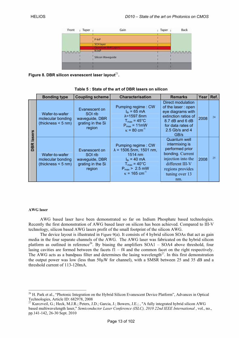
Distributed Bragg reflector (DBR) lasers are lasers where the resonator is made with at least one
distributed Bragg reflector outside the gain medium. The state of the art of DBR lasers on silicon is presented in Table 5. A schematic of the DBR
silicon evanescent laser24 is presented in Figure 8. This laser layout is very similar to the evanescent DFB laser22 except that the silicon corrugation is located outside the gain region. The laser is directly modulated, it shows open eye diagrams with extinction ratios of 8.7 dB and 6 dB for data rates of 2.5 Gb/s and 4 Gb/s.
A tunable DBR laser was also demonstrated25. The device is fabricated using quantum well intermixing where disordering of the quantum well active region is performed before bonding to shift the bandgap of the as-grown III-V material. The device utilizes two material bandgaps that have photoluminescence peaks at 1520 nm and 1440 nm. Current injection into the different III-V regions provides tuning over 13 nm.
24 A. W. Fang, B. R. Koch, R. Jones, E. Lively, D. Liang, Y.-H. Kuo, J.E. Bowers, "A Distributed Bragg Reflector Silicon Evanescent Laser," IEEE Photonics Technology Letters, 20, 1667-1669 (2008). 25 Sysak, M.N.; Anthes, J.O.; Di Liang; Bowers, J.E.; Raday, O.; Jones, R.; , "A hybrid silicon sampled grating DBR tunable laser," Group IV Photonics, 2008 5th IEEE International Conference on , vol., no., pp.55-57, 17-19 Sept. 2008
HELIOS D010 – State of the art on Photonics on CMOS
Page 13 of 102
Figure 8. DBR silicon evanescent laser layout21.
Table 5 : State of the art of DBR lasers on silicon
Bonding type Coupling scheme Characterisation Remarks Year Ref.
Wafer-to-wafer molecular bonding (thickness < 5 nm)
Evanescent on SOI rib
waveguide, DBR grating in the Si
region
Pumping regime : CW Ith = 65 mA λ=1597.6nm Tmax = 45°C
Pmax = 11mW κ = 80 cm-1
Direct modulation of the laser : open eye diagrams with extinction ratios of 8.7 dB and 6 dB for data rates of 2.5 Gb/s and 4
GB/s
2008 24
DB
R la
sers
Wafer-to-wafer molecular bonding (thickness < 5 nm)
Evanescent on SOI rib
waveguide, DBR grating in the Si
region
Pumping regime : CW λ = 1506.5nm, 1501 nm,
1514 nm Ith = 40 mA Tmax = 40°C
Pmax > 2.5 mW κ = 165 cm-1
Quantum well intermixing is
performed prior bonding. Current injection into the
different III-V regions provides tuning over 13
nm.
2008 25
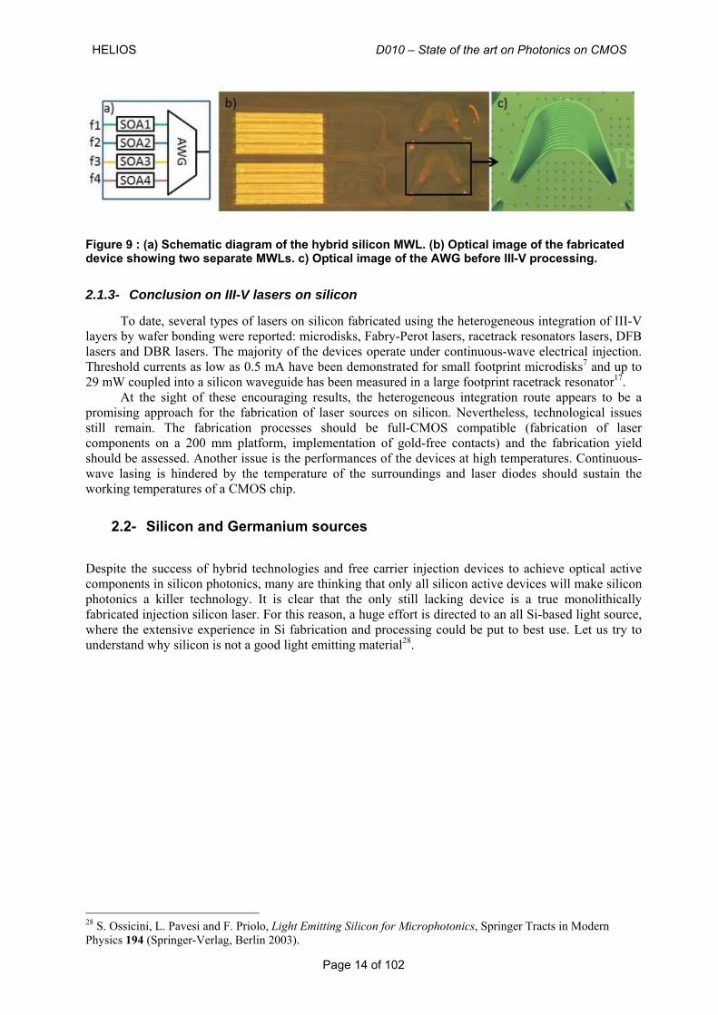
AWG laser
AWG based laser have been demonstrated so far on Indium Phosphate based technologies. Recently the first demonstration of AWG based laser on silicon has been achieved. Compared to III-V technology, silicon based AWG lasers profit of the small footprint of the silicon AWG.
The device layout is illustrated in Figure 9(a). It consists of 4 hybrid silicon SOAs that act as gain media in the four separate channels of the AWG. The AWG laser was fabricated on the hybrid silicon platform as outlined in reference26. By biasing the amplifiers SOA1 – SOA4 above threshold, four lasing cavities are formed between the facets f1 – f4 and the common facet on the right respectively. The AWG acts as a bandpass filter and determines the lasing wavelength27. In this first demonstration the output power was low (less than 50µW for channel), with a SMSR between 25 and 35 dB and a threshold current of 113-120mA.
26 H. Park et al., “Photonic Integration on the Hybrid Silicon Evanescent Device Platform”, Advances in Optical Technologies, Article ID: 682978, 2008 27 Kurczveil, G.; Heck, M.J.R.; Peters, J.D.; Garcia, J.; Bowers, J.E.; , "A fully integrated hybrid silicon AWG based multiwavelength laser," Semiconductor Laser Conference (ISLC), 2010 22nd IEEE International , vol., no., pp.141-142, 26-30 Sept. 2010
HELIOS D010 – State of the art on Photonics on CMOS
Page 14 of 102
Figure 9 : (a) Schematic diagram of the hybrid silicon MWL. (b) Optical image of the fabricated device showing two separate MWLs. c) Optical image of the AWG before III-V processing.
2.1.3- Conclusion on III-V lasers on silicon
To date, several types of lasers on silicon fabricated using the heterogeneous integration of III-V layers by wafer bonding were reported: microdisks, Fabry-Perot lasers, racetrack resonators lasers, DFB lasers and DBR lasers. The majority of the devices operate under continuous-wave electrical injection. Threshold currents as low as 0.5 mA have been demonstrated for small footprint microdisks7 and up to 29 mW coupled into a silicon waveguide has been measured in a large footprint racetrack resonator17.
At the sight of these encouraging results, the heterogeneous integration route appears to be a promising approach for the fabrication of laser sources on silicon. Nevertheless, technological issues still remain. The fabrication processes should be full-CMOS compatible (fabrication of laser components on a 200 mm platform, implementation of gold-free contacts) and the fabrication yield should be assessed. Another issue is the performances of the devices at high temperatures. Continuous-wave lasing is hindered by the temperature of the surroundings and laser diodes should sustain the working temperatures of a CMOS chip.
2.2- Silicon and Germanium sources
Despite the success of hybrid technologies and free carrier injection devices to achieve optical active components in silicon photonics, many are thinking that only all silicon active devices will make silicon photonics a killer technology. It is clear that the only still lacking device is a true monolithically fabricated injection silicon laser. For this reason, a huge effort is directed to an all Si-based light source, where the extensive experience in Si fabrication and processing could be put to best use. Let us try to understand why silicon is not a good light emitting material28.
28 S. Ossicini, L. Pavesi and F. Priolo, Light Emitting Silicon for Microphotonics, Springer Tracts in Modern Physics 194 (Springer-Verlag, Berlin 2003).
HELIOS D010 – State of the art on Photonics on CMOS
Page 15 of 102
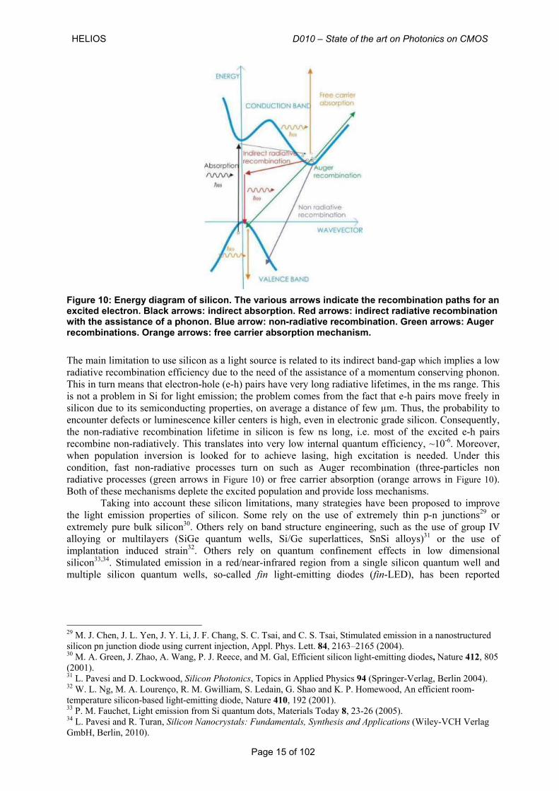
Figure 10: Energy diagram of silicon. The various arrows indicate the recombination paths for an excited electron. Black arrows: indirect absorption. Red arrows: indirect radiative recombination with the assistance of a phonon. Blue arrow: non-radiative recombination. Green arrows: Auger recombinations. Orange arrows: free carrier absorption mechanism.
The main limitation to use silicon as a light source is related to its indirect band-gap which implies a low radiative recombination efficiency due to the need of the assistance of a momentum conserving phonon. This in turn means that electron-hole (e-h) pairs have very long radiative lifetimes, in the ms range. This is not a problem in Si for light emission; the problem comes from the fact that e-h pairs move freely in silicon due to its semiconducting properties, on average a distance of few µm. Thus, the probability to encounter defects or luminescence killer centers is high, even in electronic grade silicon. Consequently, the non-radiative recombination lifetime in silicon is few ns long, i.e. most of the excited e-h pairs recombine non-radiatively. This translates into very low internal quantum efficiency, ~10-6. Moreover, when population inversion is looked for to achieve lasing, high excitation is needed. Under this condition, fast non-radiative processes turn on such as Auger recombination (three-particles non radiative processes (green arrows in Figure 10) or free carrier absorption (orange arrows in Figure 10). Both of these mechanisms deplete the excited population and provide loss mechanisms.
Taking into account these silicon limitations, many strategies have been proposed to improve the light emission properties of silicon. Some rely on the use of extremely thin p-n junctions29 or extremely pure bulk silicon30. Others rely on band structure engineering, such as the use of group IV alloying or multilayers (SiGe quantum wells, Si/Ge superlattices, SnSi alloys)31 or the use of implantation induced strain32. Others rely on quantum confinement effects in low dimensional silicon33,34. Stimulated emission in a red/near-infrared region from a single silicon quantum well and multiple silicon quantum wells, so-called fin light-emitting diodes (fin-LED), has been reported
29 M. J. Chen, J. L. Yen, J. Y. Li, J. F. Chang, S. C. Tsai, and C. S. Tsai, Stimulated emission in a nanostructured silicon pn junction diode using current injection, Appl. Phys. Lett. 84, 2163–2165 (2004). 30 M. A. Green, J. Zhao, A. Wang, P. J. Reece, and M. Gal, Efficient silicon light-emitting diodes, Nature 412, 805 (2001). 31 L. Pavesi and D. Lockwood, Silicon Photonics, Topics in Applied Physics 94 (Springer-Verlag, Berlin 2004). 32 W. L. Ng, M. A. Lourenço, R. M. Gwilliam, S. Ledain, G. Shao and K. P. Homewood, An efficient room-temperature silicon-based light-emitting diode, Nature 410, 192 (2001). 33 P. M. Fauchet, Light emission from Si quantum dots, Materials Today 8, 23-26 (2005). 34 L. Pavesi and R. Turan, Silicon Nanocrystals: Fundamentals, Synthesis and Applications (Wiley-VCH Verlag GmbH, Berlin, 2010).
HELIOS D010 – State of the art on Photonics on CMOS
Page 16 of 102
recently.35,36 The fin-LED structure is similar to the fin field-effect transistor, except for the impurity profiles and gate processes. The size of a fin is reduced down to 5 nm by an oxidation process. Silicon oxide passivated Si nanocrystals show optical gain values in a range 10-100 cm-1.37,38 Very recently, transient optical gain values up to 600 cm-1 have been observed on the picosecond time scale in silicon oxide passivated Si nanocrystals39 and up to 52 cm-1 in silicon nitride passivated Si nanocrystals under femtosecond optical pumping40.
Still another approach is impurity-mediated luminescence from, for example, isoelectronic impurities or rare earth ions. Electrically pumped Er-doped Si nanocluster gain media have attracted much attention since 1996 because of great potential for lasing at telecommunications wavelengths near 1.5 μm34. Optical material gain of 1 dB/cm41 and high fraction (20% of total Er concentration) of coupled and inverted concentration of Er ions under electrical pumping42 have been demonstrated recently. These results, together with a theoretical modal gain value of 2 dB/cm, 43 show that pulsed electrical pumping of 50-nm-thick Er-doped Si nanocluster gain medium incorporated in slot waveguides44 has big promise for achieving net gain and lasing at 1.55 um.
And yet another approach that has drawn attention recently is based on strained germanium. Germanium, which has been already widely employed with modern Si MOSFETs, has showed to be particularly interesting candidate for photonics applications, due to the fact that the epitaxial Ge-on-Si has proved to be fully compatible with all three requirements imposed on monolithically integrated light emitter on silicon45:
- The energy difference between its direct and indirect bandgaps being only 136 meV allows
engineering of its pseudo direct-gap band structure making possible realization of an efficient light emission around 1550 nm;
- It is completely compatible with standard CMOS processing technology; - Electrical pumping can be easily obtained using a diode structure due to its semiconductor
nature. It has been shown theoretically that Ge can become a direct band gap material under a 2 %
tensile strain46 . However, in this case the direct band gap shrinks to 0.53 eV at this strain magnitude, corresponding to a 2.34 μm emission wavelength47.
35 S. Saito, Y. Suwa, H. Arimoto, N. Sakuma, D. Hisamoto, H. Uchiyama, J. Yamamoto, T. Sakamizu, T. Mine, S. Kimura, T. Sugawara, and M. Aoki, “Stimulated emission of near-infrared radiation by current injection into silicon (100) quantum well,” Appl. Phys. Lett. 95, 241101 (2009) 36 S. Saito, T. Takahama, K. Tani, M. Takahashi, T. Mine, Y. Suwa, and D. Hisamoto, “Stimulated emission of near-infrared radiation in silicon fin light-emitting diode,” Appl. Phys. Lett. 98, 261104 (2011) 37 N. Daldosso and L. Pavesi, “Nanosilicon photonics,” Laser Photon. Rev. 3, 509 (2009) 38 I. Pelant, “Optical gain in silicon nanocrystals: Current status and perspectives,” Phys. Status Solidi A 208, 625-630 (2011) 39 K. Žídek, I. Pelant, F. Trojánek, P. Malý, P. Gilliot, B. Hönerlage, J. Oberlé, L. Šiller, R. Little, and B. R. Horrocks, “Ultrafast stimulated emission due to quasidirect transitions in silicon nanocrystals,” Phys. Rev. B 84, 085321 (2011) 40 B. M. Monroy, O. Cregut, M. Gallart, B. Honerlage, and P. Gilliot, “Optical gain observation on silicon nanocrystals embedded in silicon nitride under femtosecond pumping,” Appl. Phys. Lett. 98, 261108 (2011) 41 A. Pitanti, D. Navarro-Urrios, R. Guider, N. Daldosso, F. Gourbilleau, L. Khomenkova, R. Rizk and L. Pavesi, “Further improvements in Er3+ coupled to Si nanoclusters rib waveguides”, Proc. SPIE 6996, 699619 (2008) 42 O. Jambois, F. Gourbilleau, A. J. Kenyon, J. Montserrat, R. Rizk and B. Garrido, “Towards population inversion of electrically pumped Er ions sensitized by Si nanoclusters,” Opt. Express 18, 2230-2235 (2010) 43 G. M. Miller, R. M. Briggs and H. A. Atwater, “Achieving optical gain in waveguide-confined nanocluster-sensitized erbium by pulsed excitation”, J. Appl. Phys. 108, 063109 (2010) 44 K. Preston and M. Lipson, “Slot waveguides with polycrystalline silicon for electrical injection”, Opt. Express 17, 1527-1534 (2009) 45 Xiaochen Sun, Jifeng Liu, Lionel C. Kimerling and Jurgen Michel, “Band-engineered Ge for Si-based light emitter”, 214th ECS Meeting, Abstract #2473 (2008) 46 M.V. Fischetti and S. E. Laux, “Band structure, deformation potentials, and carrier mobility in strained Si, Ge, and SiGe alloys,” J. Appl. Phys. 80, 2234 (1996) 47 M. El Kurdi, G. Fishman, S. Sauvage and P. Boucaud, "Band structure and optical gain of tensile-strained germanium based on a 30 band k⋅p formalism", J. Appl. Phys. 107, 013710 (2010)
HELIOS D010 – State of the art on Photonics on CMOS
Page 17 of 102
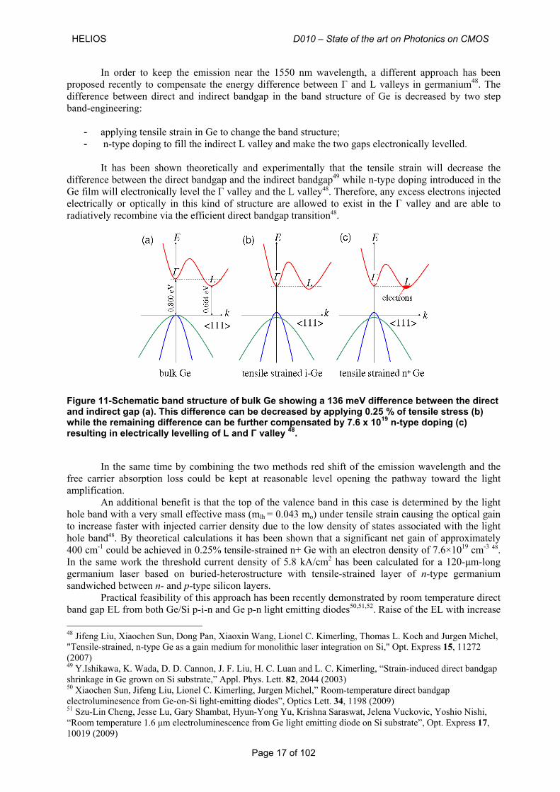
In order to keep the emission near the 1550 nm wavelength, a different approach has been proposed recently to compensate the energy difference between Γ and L valleys in germanium48. The difference between direct and indirect bandgap in the band structure of Ge is decreased by two step band-engineering:
- applying tensile strain in Ge to change the band structure; - n-type doping to fill the indirect L valley and make the two gaps electronically levelled.
It has been shown theoretically and experimentally that the tensile strain will decrease the difference between the direct bandgap and the indirect bandgap49 while n-type doping introduced in the Ge film will electronically level the Γ valley and the L valley48. Therefore, any excess electrons injected electrically or optically in this kind of structure are allowed to exist in the Γ valley and are able to radiatively recombine via the efficient direct bandgap transition48.
Figure 11-Schematic band structure of bulk Ge showing a 136 meV difference between the direct and indirect gap (a). This difference can be decreased by applying 0.25 % of tensile stress (b) while the remaining difference can be further compensated by 7.6 x 10¹⁹ n-type doping (c) resulting in electrically levelling of L and Γ valley 48.
In the same time by combining the two methods red shift of the emission wavelength and the free carrier absorption loss could be kept at reasonable level opening the pathway toward the light amplification.
An additional benefit is that the top of the valence band in this case is determined by the light hole band with a very small effective mass (mlh = 0.043 mo) under tensile strain causing the optical gain to increase faster with injected carrier density due to the low density of states associated with the light hole band48. By theoretical calculations it has been shown that a significant net gain of approximately 400 cm-1 could be achieved in 0.25% tensile-strained n+ Ge with an electron density of 7.6×1019 cm-3 48. In the same work the threshold current density of 5.8 kA/cm2 has been calculated for a 120-μm-long germanium laser based on buried-heterostructure with tensile-strained layer of n-type germanium sandwiched between n- and p-type silicon layers.
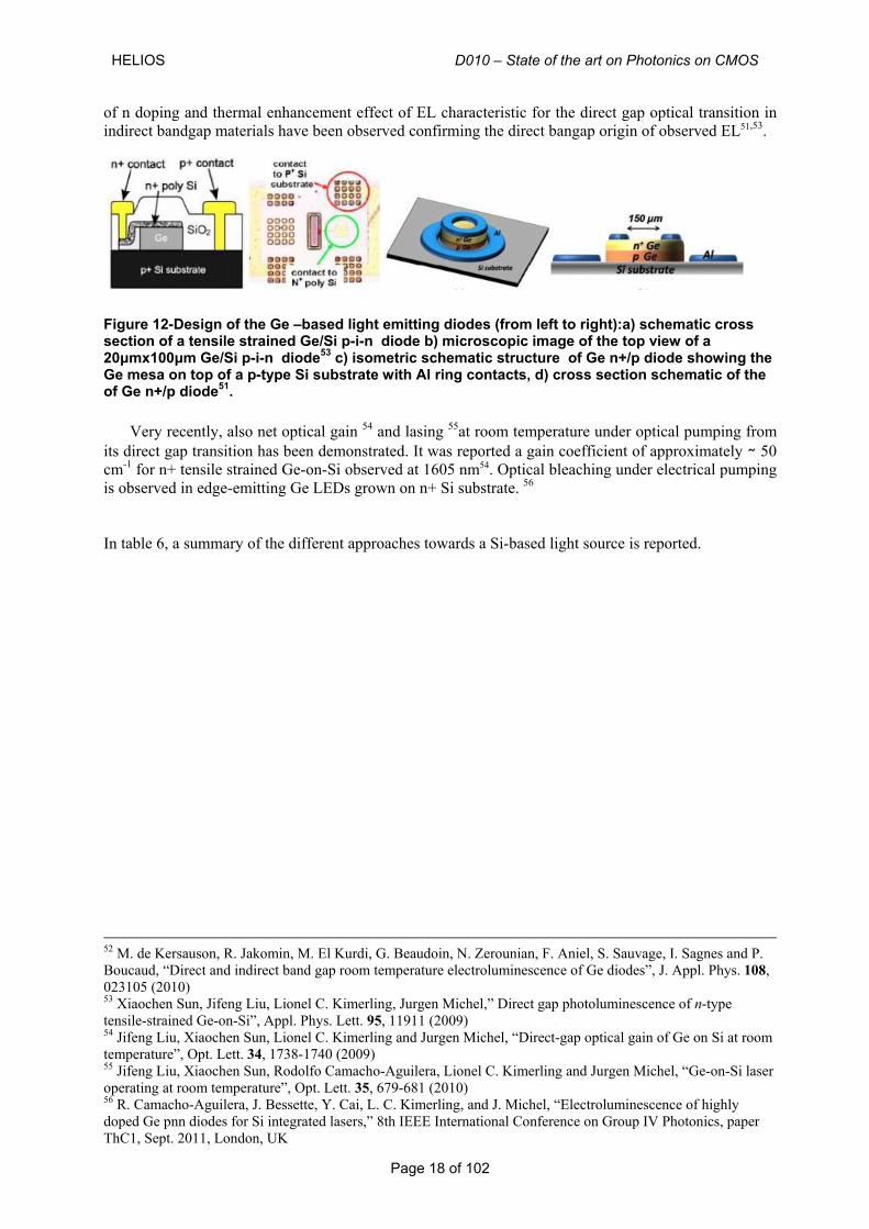
Practical feasibility of this approach has been recently demonstrated by room temperature direct band gap EL from both Ge/Si p-i-n and Ge p-n light emitting diodes50,51,52. Raise of the EL with increase 48 Jifeng Liu, Xiaochen Sun, Dong Pan, Xiaoxin Wang, Lionel C. Kimerling, Thomas L. Koch and Jurgen Michel, "Tensile-strained, n-type Ge as a gain medium for monolithic laser integration on Si," Opt. Express 15, 11272 (2007) 49 Y.Ishikawa, K. Wada, D. D. Cannon, J. F. Liu, H. C. Luan and L. C. Kimerling, “Strain-induced direct bandgap shrinkage in Ge grown on Si substrate,” Appl. Phys. Lett. 82, 2044 (2003) 50 Xiaochen Sun, Jifeng Liu, Lionel C. Kimerling, Jurgen Michel,” Room-temperature direct bandgap electroluminesence from Ge-on-Si light-emitting diodes”, Optics Lett. 34, 1198 (2009) 51 Szu-Lin Cheng, Jesse Lu, Gary Shambat, Hyun-Yong Yu, Krishna Saraswat, Jelena Vuckovic, Yoshio Nishi, “Room temperature 1.6 μm electroluminescence from Ge light emitting diode on Si substrate”, Opt. Express 17, 10019 (2009)
HELIOS D010 – State of the art on Photonics on CMOS
Page 18 of 102
of n doping and thermal enhancement effect of EL characteristic for the direct gap optical transition in indirect bandgap materials have been observed confirming the direct bangap origin of observed EL51,53.
Figure 12-Design of the Ge –based light emitting diodes (from left to right):a) schematic cross section of a tensile strained Ge/Si p-i-n diode b) microscopic image of the top view of a 20μmx100μm Ge/Si p-i-n diode53 c) isometric schematic structure of Ge n+/p diode showing the Ge mesa on top of a p-type Si substrate with Al ring contacts, d) cross section schematic of the of Ge n+/p diode51.
Very recently, also net optical gain 54 and lasing 55at room temperature under optical pumping from its direct gap transition has been demonstrated. It was reported a gain coefficient of approximately 50 cm-1 for n+ tensile strained Ge-on-Si observed at 1605 nm54. Optical bleaching under electrical pumping is observed in edge-emitting Ge LEDs grown on n+ Si substrate. 56
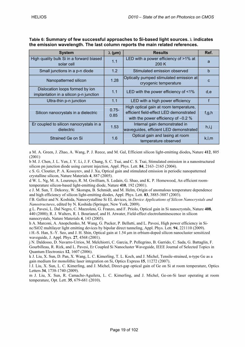
In table 6, a summary of the different approaches towards a Si-based light source is reported.
52 M. de Kersauson, R. Jakomin, M. El Kurdi, G. Beaudoin, N. Zerounian, F. Aniel, S. Sauvage, I. Sagnes and P. Boucaud, “Direct and indirect band gap room temperature electroluminescence of Ge diodes”, J. Appl. Phys. 108, 023105 (2010) 53 Xiaochen Sun, Jifeng Liu, Lionel C. Kimerling, Jurgen Michel,” Direct gap photoluminescence of n-type tensile-strained Ge-on-Si”, Appl. Phys. Lett. 95, 11911 (2009) 54 Jifeng Liu, Xiaochen Sun, Lionel C. Kimerling and Jurgen Michel, “Direct-gap optical gain of Ge on Si at room temperature”, Opt. Lett. 34, 1738-1740 (2009) 55 Jifeng Liu, Xiaochen Sun, Rodolfo Camacho-Aguilera, Lionel C. Kimerling and Jurgen Michel, “Ge-on-Si laser operating at room temperature”, Opt. Lett. 35, 679-681 (2010) 56 R. Camacho-Aguilera, J. Bessette, Y. Cai, L. C. Kimerling, and J. Michel, “Electroluminescence of highly doped Ge pnn diodes for Si integrated lasers,” 8th IEEE International Conference on Group IV Photonics, paper ThC1, Sept. 2011, London, UK
HELIOS D010 – State of the art on Photonics on CMOS
Page 19 of 102
Table 6: Summary of few successful approaches to Si-based light sources. λ indicates the emission wavelength. The last column reports the main related references.
System λ (µm) Results Ref. High quality bulk Si in a forward biased
solar cell 1.1 LED with a power efficiency of >1% at 200 K a
Small junctions in a p-n diode 1.2 Stimulated emission observed b
Nanopatterned silicon 1.28 Optically pumped stimulated emission at cryogenic temperature c
Dislocation loops formed by ion implantation in a silicon p-n junction 1.1 LED with the power efficiency of <1% d,e
Ultra-thin p-n junction 1.1 LED with a high power efficiency f
Silicon nanocrystals in a dielectric 0.75-0.85
High optical gain at room temperature, efficient field-effect LED demonstrated
with the power efficiency of ∼0.2 % f,g,h
Er coupled to silicon nanocrystals in a dielectric 1.53 Internal gain demonstrated in
waveguides, efficient LED demonstrated h,i,j
Strained Ge on Si 1.6 Optical gain and lasing at room temperature observed k,l,m
a M. A. Green, J. Zhao, A. Wang, P. J. Reece, and M. Gal, Efficient silicon light-emitting diodes, Nature 412, 805 (2001) b M. J. Chen, J. L. Yen, J. Y. Li, J. F. Chang, S. C. Tsai, and C. S. Tsai, Stimulated emission in a nanostructured silicon pn junction diode using current injection, Appl. Phys. Lett. 84, 2163–2165 (2004). c S. G. Cloutier, P. A. Kossyrev, and J. Xu, Optical gain and stimulated emission in periodic nanopatterned crystalline silicon, Nature Materials 4, 887 (2005). d W. L. Ng, M. A. Lourenço, R. M. Gwilliam, S. Ledain, G. Shao, and K. P. Homewood, An efficient room-temperature silicon-based light-emitting diode, Nature 410, 192 (2001). e J. M. Sun, T. Dekorsy, W. Skorupa, B. Schmidt, and M. Helm, Origin of anomalous temperature dependence and high efficiency of silicon light-emitting diodes, Appl. Phys. Lett. 83, 3885-3887 (2003). f B. Gelloz and N. Koshida, Nanocrystalline Si EL devices, in Device Applications of Silicon Nanocrystals and Nanostructures, edited by N. Koshida (Springer, New York, 2009). g L. Pavesi, L. Dal Negro, C. Mazzoleni, G. Franzo, and F. Priolo, Optical gain in Si nanocrystals, Nature 408, 440 (2000); R. J. Walters, R. I. Bourianof, and H. Atwater, Field-effect electroluminescence in silicon nanocrystals, Nature Materials 4, 143 (2005). h A. Marconi, A. Anopchenko, M. Wang, G. Pucker, P. Bellutti, and L. Pavesi, High power efficiency in Si-nc/SiO2 multilayer light emitting devices by bipolar direct tunneling, Appl. Phys. Lett. 94, 221110 (2009). i H.-S. Han, S.-Y. Seo, and J. H. Shin, Optical gain at 1.54 μm in erbium-doped silicon nanocluster sensitized waveguide, J. Appl. Phys. 27, 4568 (2001). j N. Daldosso, D. Navarro-Urrios, M. Melchiorri, C. Garcia, P. Pellegrino, B. Garrido, C. Sada, G. Battaglin, F. Gourbilleau, R. Rizk, and L. Pavesi, Er Coupled Si Nanocluster Waveguide, IEEE Journal of Selected Topics in Quantum Electronics 12, 1607 (2006). k J. Liu, X. Sun, D. Pan, X. Wang, L. C. Kimerling, T. L. Koch, and J. Michel, Tensile-strained, n-type Ge as a gain medium for monolithic laser integration on Si, Optics Express 15, 11272 (2007). l J. Liu, X. Sun, L. C. Kimerling, and J. Michel, Direct-gap optical gain of Ge on Si at room temperature, Optics Letters 34, 1738-1740 (2009). m J. Liu, X. Sun, R. Camacho-Aguilera, L. C. Kimerling, and J. Michel, Ge-on-Si laser operating at room temperature, Opt. Lett. 35, 679-681 (2010).
HELIOS D010 – State of the art on Photonics on CMOS
Page 20 of 102
2.3- 2.5D sources
When combined with low index media (such as, for example, silica), along a variety of high index contrast nano-structuration schemes, the heterogeneous integration of III-V and Silicon semiconductor materials may result in photonic nanostructures with remarkable optical confinement properties, allowing for a very efficient control over photons in time and space. III-V semiconductors can, in addition, offer their unique emission and non-linear characteristics, which are missing to silicon. Two confinement schemes based on high index contrast structures are presently considered: - The high index contrast refractive confinement scheme, where total internal reflection of photons is
used to confine them inside the high index material: this approach is essentially restricted to in plane wave-guiding micro-nano-photonic devices.
- The Photonic Crystal diffractive confinement scheme, which can be combined in part with the refractive approach; this approach may apply to both in-plane wave-guiding and free space surface operating devices.
As to the diffractive confinement scheme, the group at INL, in collaboration with CEA-LETI, has pioneered the demonstration of different families of Photonic Crystal based micro-lasers, formed in III-V semiconductor membranes bonded on silica on silicon substrate57, 58, 59. Although the silicon material was simply used as a plain substrate, this is to be considered as the first and necessary step towards the real III-V / silicon heterogeneous and functional integration of diffractive photonic structures. In the prospective section of the present project, we propose to develop an innovative technological/conceptual scheme for 3D microphotonics on CMOS combining III-V/Silicon heterogeneous integration and diffractive photonics. It is based on the use of a standard generic technological building block, along a so called 2.5D approach, and opens the way to far larger functionality and wider potential impact than other schemes reported so far60. This has been confirmed recently with the demonstration of a novel class of hybrid VCSEL devices, operating along these new conceptual schemes, by INL (InP material system61,62,63), together with the group at UC Berkeley (GaAs material system)64,65. 57 C. Monat, C. Seassal, X. Letartre, P. Viktorovitch, P. Regreny, M. Gendry, P. Rojo-Romeo, G. Hollinger , E. Jalaguier, S. Pocas, B. Aspar, InP 2D photonic crystal microlasers on silicon wafer : room temperature operation at 1.55µm, Electron. Letters 37, 764 (2001) 58 C. Monat, C. Seassal, X. Letartre, P. Regreny, P. Rojo-Romeo, P. Viktorovitch, M. Le Vassor D’yerville, D. Cassagne, J.P. Albert, E. Jalaguier, S. Pocas, B. Aspar, “InP based 2D Photonic Crystal on silicon: in-plane Bloch mode laser”, Appl. Phys. Letters 81, 5102 (2002) 59 J. Mouette, C. Seassal, X. Letartre, P. Rojo-Romeo, J.-L. Leclercq, P. Regreny, P. Viktorovitch, E. Jalaguier, P. Perreau, H. Moriceau, « Very low threshold vertical emitting laser operation in InP graphite photonic crystal slab on silicon”, Electron. Lett 39, 526 (2003) 60 Pierre Viktorovitch, Badhise Ben Bakir, Salim Boutami, Jean-Louis Leclercq, Xavier Letartre, Pedro Rojo-Romeo, Christian Seassal, Marc Zussy, Lea Di Cioccio, Jean-Marc Fedeli, 3D harnessing of light with 2.5D photonic crystals, Laser Photonic Reviews, 1–13 (2009) 61 S. Boutami, B. Ben Bakir, J.-L. Leclercq, P. Viktorovitch, “Compact and polarization controlled 1.55µm vertical-cavity surface emitting laser using single-layer Photonic Crystal mirror”, Appl. Phys. Lett. 91, 071105 (2007). 62 Badhise Ben Bakir, Salim Boutami, Christian Seassal, Xavier Letartre, Jean-Louis Leclercq, Pierre Viktorovitch, Marc Zussy, Léa Di Cioccio, Jean M. Fedeli, « Control of mode volume and radiation dynamics of a slow-light-mode in a quasi-3D Photonic Crystal configuration », invited paper, Photonics Europe, 7-10 avril 2008, Strasbourg (France), SPIE proceedings, paper 6989 OM. 63 P. Viktorovitch, Jean-Louis Leclercq, Xavier Letartre, Pedro Rojo-Romeo, Christian Seassal, “Photonic Crystal based surface emitting micro-lasers”, invited paper, LPHYS’09, 13-17 July 2009 (Barcelona) 64 C. Y. Huang, Y. Zhou, and C. J. Chang-Hasnain, “A surface-emitting laser incorporating a high-index-contrast subwavelength grating”, Nat. Photonics 1, 119 (2007). 65 Vadim Karagodsky, Bala Pesala, Christopher Chase, Werner Hofmann, Fumio Koyama and Connie J. Chang-Hasnain, Optics Express 18, 694 (2010)
HELIOS D010 – State of the art on Photonics on CMOS
Page 21 of 102
Vertical-cavity surface-emitting lasers (VCSELs) using hybrid III-V / Si microcavities and based on double photonic crystal reflectors for the heterogeneous integration on complementary metal-oxide-silicon (CMOS) have been demonstrated, for the first time, in the frame of HELIOS project. High fabrication yield relying on state-of-the-art wafer bonding technology has been achieved. Room-temperature single-mode laser operation at 1.55-µm has been obtained in compact devices (about 3-µm-thick and 15x15 µm2 in lateral area), both in pulsed and continuous-wave regimes, under optical pumping. Thresholds in the sub-mW range have been achieved owing to an optimized management of device optical losses and thermal features66,67.
3- Modulators
3.1- Packaged modulator on the market
3.1.1- High speed semiconductor MZI modulators
Due to their optical properties and potential for optoelectronics integration, Indium Phosphide (InP) and gallium arsenide (GaAs) semiconductors are playing a major role for future optical communications. One of their properties is the lack of symmetry of the crystal structure (Zinc Blende). In other words, III-V semiconductors of the GaAs or InP family possess a linear electro-optic effect. Thus, it is possible to take advantage of this property to design high-speed intensity modulators. Despite the relative poor value of the only non-zero bulk electro-optic coefficient (r41=1.4pm/V), the high refractive index (n≅3.4) joined with a nearly 100% overlap between the optical and electrical field give a good electro-optic efficiency (comparable to existing lithium niobate devices). For example, a voltage-length product (VπLπ) of the order of 9V.cm has been already published and the value of 5.5V.cm seems to be reachable. The main supplier of III-V Mach-Zehnder modulators is Oclaro. The Company U2T recently released they acquired a III-V technology for Mach-Zehnder modulator fabrication on GaAs substrate. Optical waveguides The principle of intensity modulation is based on the classical integrated Mach-Zehnder interferometer. A Y junction, or multimode interference section (MMI) divides the optical guided wave in each arm. The relative phase of the guided wave is controlled by an electric field signal generated via metallic electrodes. By reconstruction at the end of the device (new Y junction or MMI) phase modulation is converted into intensity modulation. The optical wave is guided vertically by a structure of layers with different refractive indices: a higher index layer called the “core” is sandwiched between two “claddings” with lower indices. Due to their lower refractive indices compared with GaAs or InP, ternary (AlxGa(1-x)As for GaAs substrates) or quaternary compound (InxGa(1-x)AsyP(1-y) for InP substrates) semiconductors are chosen for the claddings. The core layer is composed of GaAs or InP. Those layers are produced using an epitaxial 66 C. Sciancalepore, B. Ben Bakir, X. Letartre, J.-M. Fedeli, N. Olivier, D. Bordel, C. Seassal, P. Rojo-Romeo, P. Regreny, and P. Viktorovitch, “Quasi-3D light confinement in double photonic crystal reflectors VCSELs for CMOS-compatible integration,” IEEE J. of Lightw. Technol., 29, 13, 2015–2024 (2011) 67 Corrado Sciancalepore, Badhise Ben Bakir, Xavier Letartre, Nicolas Olivier, Christian Seassal, Damien, Bordel, Pedro Rojo-Romeo, Member, IEEE, Philippe Regreny, Jean-Marc Fedeli, and Pierre Viktorovitch, CMOS-Compatible Integration of III-V VCSELs Based on Double Photonic Crystal Reflectors, Group Four Phootnics 2011, London (14-16 September 2011)
HELIOS D010 – State of the art on Photonics on CMOS
Page 22 of 102
growth on the substrate. Different techniques such as metal organic chemical vapor deposition (MOCVD) or molecular beam epitaxy (MBE) are available for that operation. Adequate lateral confinement is imposed by means of ribs etched (by reactive ion etching or chemically) just through the upper cladding layer. Typical rib widths are in the 3-6 µm range and rib heights in the micrometer range. One of the determinant parameters in the design of an optical modulator is the optical losses. In III-V semiconductors, mode mismatch losses between the optical mode of the waveguide and the fiber are actually high (over 10 dB) compared to other materials (below 1dB for LiNbO3). Therefore, designers frequently insert an integrated mode expander on the component. Linear electro-optic effect The most common crystallographic orientation of growth is (001). In that case, phase modulation of the optical guided wave occurs when a vertical electric field is applied:
LErn zTE ηλπφ 41
3±= (1)
where λ is the optical wavelength, n is the refractive index, 41r is the bulk linear electro-optic coefficient, zE is the vertical component of the electric field and L is the length of interaction. The normalized factor η corresponds to the overlap coefficient between the electrical field and the optical field. Note that in this case, only quasi-TE polarized light is modulated. Electro-optic modulation is thus polarization dependent. Moreover, a high-speed polarization independent scheme has been already demonstrated. Two different ways are possible for the generation of the electric field:
o The reverse-biased Schottky -i-n junction: A differential voltage is applied between the top metallic electrodes (Schottky contact) and the n+-type back contact. The main advantages of this structure are associated with a good overlap between the electrical and optical fields (η ), thus giving a low Vπ and a nearly voltage-invariant capacitance
o The double Schottky contacts: The presence of the electrical contacts on top, the undoped
epilayers and the substrate create a large depleted area with a low conductivity, which is coinciding with the waveguide. When a time- varying voltage is applied on the electrodes, the depleted areas begin to behave as lossy dielectrics, and [001] electric fields of opposite polarity are applied on the optical guides. The situation becomes similar to the case of electrodes on a dielectric material like lithium niobate. The use of such undoped epilayers has allowed chirp-free modulation in excess of 40 GHz but at the price of a medium overlap factor ( 5.0≈η ).
In spite of these differences, these two structures can be operated in a push-pull configuration (in series for the first case and parallel for the second case) in order to enhance efficiency. Compatibility with very high-speed modulation: travelling-wave design strategy Another important parameter for the design of very high-speed modulators is the electro-optic bandwidth, which governs the speed of modulation. For that case, special electrodes called “travelling-wave electrodes” are designed. These electrodes are considered as transmission lines for the modulating voltage (microwave signal). Three parameters must be simultaneously optimised for the design of travelling-wave electrodes:
o Impedance matching of the line to the driving circuit (50 Ω typically). o Low microwave propagation losses of the signal. o Velocity matching between the optical wave and the microwave signal.
HELIOS D010 – State of the art on Photonics on CMOS
Page 23 of 102
The aim in travelling-wave is to achieve a modulating microwave voltage, which propagates at the same velocity and in the same direction as the optical wave. According to those conditions, phase modulation can accumulate monotonically along the direction of propagation. Because the effective index of the modulating microwave μn (2.63) is lower than the effective index of the modulating optical effn (3.4), in III-V compound semiconductors, velocity matching requires slowing down the microwave signal. The most commonly used technique to slow down the signal is to use slow-wave electrodes (SWE). The structure is based on a modified coplanar line combined with T-rails (narrow fins and pads) on each side. These fins and pads introduce distributed capacitance and thereby reduce the speed of the microwave signal. The main drawback of such a structure is a lowering of the electro-optical efficiency depending on the length of the active sections. Structures of SWE usually employed are the capacitively loaded coplanar strip line (SW-CPS) or the capacitively loaded coplanar waveguide line (SW-CPW). Therefore, a low-loss velocity- and impedance-matched electrode is essential for the realization of ultra-wide-bandwidth travelling-wave modulators. Criteria of selection
o High potential of integration when complex functions are necessary: all optical functions can be inserted on the same chip in order to lower insertion losses, gain stability and reduce the size of the system.
o Optical waveguides easily modified by the control of the size of the ribs. o Optical waveguides can handle very large amount of powers since they are very similar to
semiconductors lasers that generate very high powers. Practical limit of the power handling capability is the catastrophic facet damage.
o Good overlap between the electrical and the optical fields, which enable low drive voltages. o Injection facets cleaved. o Optical refractive index higher than the microwave index ( effnn pμ ). Velocity Matching
requires slowing down the microwave signal. Utilization of slow-wave electrodes with periodically loading elements is a solution. Thus, velocity matching is obtained with relatively thin electrodes (typically 1µm), which simplify the technological process.
o For the SWE, the distance between the centre conductor and the ground plane of the unloaded line determines the microwave loss. It is thus possible to obtain simultaneously a low microwave loss (a large gap between unloaded lines) and a high electric field (a small gap between the T-rails).
o Bulk linear electro-optic coefficient low (1.4 pm/V) compared to other materials (Lithium
niobate or polymers). o High Fibre/waveguide losses: implementation of an integrated mode expander is necessary or
direct connection to a laser. Due to high insertion loss, the modulator is commercialised by Bookham with the laser integrated in the same package, under a hybrid configuration.
o SWE with periodically loading elements. Only a fraction of the total electrode length is electro optically active.
o MBE or MOCVD systems cost.
3.1.2- Lithium Niobate Electro-optic Modulators
Lithium niobate (LiNbO3) electro-optic modulators are used as external devices to implement intensity-modulated optical transmissions. In such a case, the optical power emitted by a light source is constant and it can be modulated when passing through external optical waveguides on LiNbO3 electro-optic crystals. Electrical modulation can be imprinted on light taking advantage of the intrinsic LiNbO3 electro-optic coefficients. Optical intensity modulators are typically based on integrated optics Mach-Zehnder interferometers. To achieve a wide-band modulation capability, Mach-Zehnder modulators are
HELIOS D010 – State of the art on Photonics on CMOS
Page 24 of 102
provided with travelling-wave electrodes. Merit figures in LiNbO3 modulators are the half-wave voltage, the electro-optic frequency response, optical insertion losses, thermal stability, photo refractive sensitivity, bias stability, etc. Up to date, state of art LiNbO3 external modulators present electrical an optical performances to transmit information data rates of 2.5, 10 and potentially 40 Gb/s. Technology for LiNbO3 external modulators is the most mature and insure optimal performances for maximum data rates. However, important trade-offs need to be considered, mainly related to half-wave voltages, electro-optical bandwidths, static and dynamic extinction ratio, chirp figures, among others, in order to conform to transmission specifications. The main suppliers today are JDSU, Avanex, Sumitomo, Photline, and EOSPACE Mach-Zehnder modulator operating principle The basic structure includes a Mach-Zehnder interferometer based on a two-arm optical waveguide geometry, which is joined at its extremities by Y-branches allowing both to split and to recombine light. Mach-Zehnder electro-optic modulators are fabricated on both Z or X cut and Y-propagating LiNbO3 substrates. To optimise the electro-optic interaction and hence the optical modulation, light must be polarized in the direction of the largest electro-optic coefficient (r33). To achieve a wide-band modulation capability, Mach-Zehnder modulators are designed with travelling-wave electrodes. In this case, electrodes act as transmission lines and the most common structure is a coplanar wave-guide (CPW). The operating principle of a Mach-Zehnder modulator is as follows: Light entering the input optical waveguide is split by the first Y-junction and it propagates through the two parallel waveguide sections which are used as optical phase modulators. At the output of the Y-junction, the two light fields recombine and variable interference can be observed if a differential phase is present between the two parallel arms. In this way, optical intensity modulation can be achieved by modifying the optical phase on one of the optical waveguides by applying an external electric field, taking advantage of the electro-optic effect in the LiNbO3 crystal. The external electric field is generated by applying a time-varying voltage by means of the travelling wave modulating electrodes. Universal electrical compatibility imposes that the travelling wave electrodes be designed to match 50 Ω standard devices. The half-wave voltage is given as:
lrnsV Γ= 333/λπ
Where λ is the optical wave-length, s is the electrode gap, n is the optical refractive index, r is the electro-optic coefficient, Γ is the electric-optic overlap coefficient and l is the electrode length. The lowest half-wave voltages can be obtained using Z-cut LiNbO3 substrates. For a particular crystal cut, handling either the length or the gap of the modulating electrodes can change the half-wave voltage. Today, on X-cut devices, typical values between 5 and 6 volts can be obtained for 30 mm electrode lengths and 10-20 microns gap. Continued effort in design and technology are conducted to further decrease the half-wave voltage. Much lower voltages are really attractive for 40 Gb/s devices. Static Optical extinction ratio The static optical extinction ratio of the electro-optic modulator, deduced from its optical transfer function is another critical parameter .After an optimised fabrication process, this parameter can range between 25 and 35 dB, for a high performances electro-optic modulator. The electric-optical velocity mismatch A major trade-off for maximum modulation bandwidth is related to the electrical-optical velocity mismatch, as determined by the difference in effective index inside the electro-optic crystal ( 2.2=n ) and on the crystal-air interface ( 2.4=nμ ). Light propagating inside the optical waveguide travels
HELIOS D010 – State of the art on Photonics on CMOS
Page 25 of 102
faster than the electric wave travelling on its surface. Under perfect matching conditions, the frequency response is only limited by the electrical losses on the electrodes. The velocity mismatch needs to be drastically reduced for reaching a wide-band frequency response. The most common practical approach is based on the association of a thin buffer layer of silicon dioxide (SiO2), coating the surface of the LiNbO3 crystal, and thick gold travelling electrodes, electroplated on the top of the buffer layer. This combination decreases the microwave effective index and consequently the velocity mismatch also decreases. Such an approach is easy to implement in technology and flat electro-optic frequency responses near 40 GHz have been reported. More elaborated solutions showing frequency responses near to 100 GHz have also been proposed. Chirp The chirp parameter in optical modulators is another critical figure of merit for transmitting high data rates in dispersive optical fibre. Chirp represents an unwanted phase shift, which appears when light intensity is modulated. Chirp causes light pulses broadening and hence it limits the maximum frequency response of an optical link. Chirp is present in most optical modulators and its reduction to weak levels is an important issue. In the case of external modulators, chirp is generally lower than in directly modulated lasers. Lithium Niobate modulators can exhibit very low chirp and X-cut devices are theoretically chirp-free devices. In such X-cut devices, optimised fabrication parameters regarding symmetry of waveguides and electrodes, give chirp parameters between 1.0± . These low values of chirp are opening a wide utilization of external modulators for the highest data rates in today and near future telecommunication markets. Technology and fabrication of electro-optic modulators The optical waveguides are fabricated on a X-cut LiNbO3 substrate by titanium coating and in-diffusion at temperatures as high as 1100 °C. The Ti ions modify the ordinary and extraordinary refractive index in the crystal. Careful design of the in diffusion process allows the creation of an index gradient to define a low-loss, single mode optical channels. Typical widths and depths for single mode optical channels range between 3 to 8 microns. This channel will guide light along the crystal. . In a second step, a thin SiO2 buffer layer will coat the LiNbO3 crystal surface. This buffer layer enhances electric-optical phase matching and prevents high optical losses for the TM optical mode. On this buffer layer, the travelling wave electrodes are grown by gold plating. The gold electrodes are relatively thick (15-20 microns) in order to insure the minimal electric losses. Electrode width and gap are defined to give near-50 Ω characteristic impedance. The following steps in the fabrication process include dicing and polishing of the optical chips. Polishing of the input-output optical faces in the crystal represents a critical step to be optimised for minimal optical losses. Fibre pig tailing at the end of the fabrication process is required for light to be injected and modulated by the electro-optic device. Once the electro-optic chip is pigtailed, packaging is carried out. RF and optical connectors are specified and mounted. For 10 Gb/s devices, K-electrical and FC/PC optical connectors are often specified. Design and fabrication tools allow today to realize very compact devices, just limited in dimension (3") by the expected optimal performances. Most effort has been concentrated in developing new techniques to increase bandwidth. It is now possible to implement high performance 10 Gb/s optical links. In the near future, further progress will permit the transmission of data rates as high as 40 Gb/s. Commercial devices are currently proposed to work on standardized 10 Gb/s optical fibre links with low driving voltages below 4V, and very low insertion loss (<3dB). Several hundreds of thousand of LN modulators have been deployed during the past 10 years. These devices are now fully tested filling the
HELIOS D010 – State of the art on Photonics on CMOS
Page 26 of 102
stringent transmission specifications. The size is the main limitations of lithium niobate modulators (<70mm for the most compact version) Technology LiNbO3 InP Half-wave voltage Vπ RF port @ DC @ 1540 nm <3.7V 2,7V Effective Half-wave voltage Vπ RF Port @ Data rate @ 1540 nm
<4.5V
Half-wave voltage Vπ DC port @ 1540 nm Typ 5V Microwave S11 return loss 0.13GHz –20GHz <-10dB <-10dB Electro-optical bandwidth @ -3dB 12-16 GHz 10GHz Ripple <1dB <1dB Optical Insertion loss (fiber to fiber) <4dB >9dB Optical return loss <-35 dB <-35 dB Dynamic Extinction ratio at 10 Gb/s >15dB >11.5dB Chirp <0.1 -0.7 Max optical input power +20 dBm +20 dBm Wavelength range 1520-1620 nm C+L 1520-1620 nm C+L Packaging Input PM Fiber type DFB Laser Output fiber SMF or PMF type Input RF connector 50 Female K or GPO Optical Connector FC/PC or FC/APC FC/PC or FC/APC Fiber length 1 meter (typ.) 1 meter (typ.) Chip length 50mm Few mm Package type Examples 70mm 14-pin Dil or butterfly Termination Impedance Internal Internal Storage Temperature -40°C +85°C -40°C +85°C
3.2- Overview on modulators on silicon
Silicon microphotonics has generated an increasing interest in the recent years. Integrating optics and electronics on a same chip would allow the enhancement of integrated circuit (IC) performances. Furthermore, telecommunications could benefit from the development of low cost solutions for high-speed optical links. The realization of active photonic devices, in particular high speed optical modulators integrated in silicon-on-insulator (SOI) waveguides is essential for the development of silicon microphotonics. Although silicon does not in normal circumstances exhibit an electro-optic effect, other mechanisms are available for modulation which includes the thermo-optic and plasma dispersion effects. Aside from these, further interesting methods have been reported which include using strain to introduce an electro-optic effect68, forming SiGe/Ge quantum wells to take advantage of the quantum-confined stark effect69 and bonding III-V materials to make use of their stronger electro-optic properties70,71. 68 Jacobsen, R.S., et al., Strained silicon as a new electro-optic material. Nature, 2006. 441(7090): p. 199-202. 69 Kuo, Y.-H., et al., Strong quantum-confined Stark effect in germanium quantum-well structures on silicon. Nature, 2005. 437(7063): p. 1334-1336. 70 Kuo, Y.-H., H.-W. Chen, and J.E. Bowers, High speed hybrid silicon evanescent electroabsorption modulator. Optics Express, 2008. 16(13): p. 9936-9941. 71 Liu, L., et al. Carrier-injection-based electro-optical modulator on SOI with a heterogeneously integrated III-V microdisk cavity. 2008
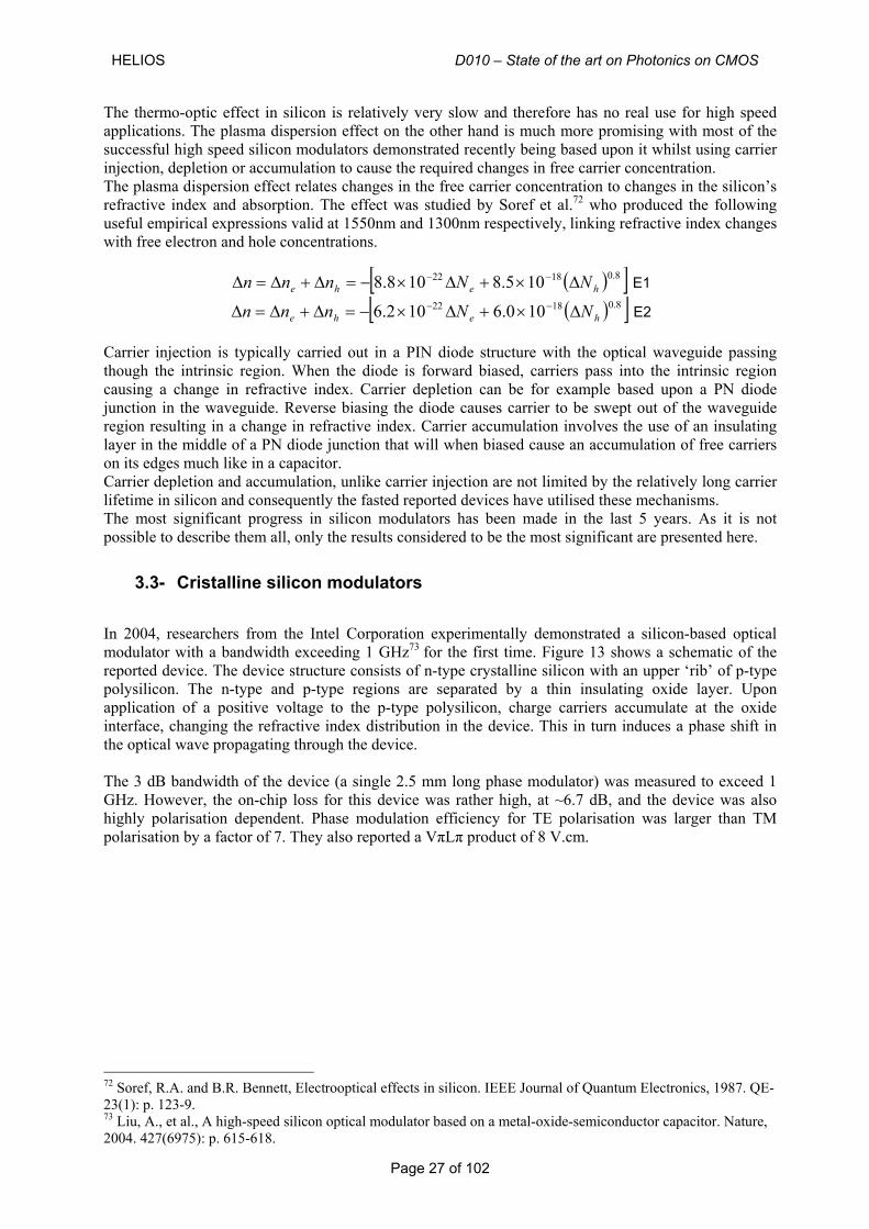
HELIOS D010 – State of the art on Photonics on CMOS
Page 27 of 102
The thermo-optic effect in silicon is relatively very slow and therefore has no real use for high speed applications. The plasma dispersion effect on the other hand is much more promising with most of the successful high speed silicon modulators demonstrated recently being based upon it whilst using carrier injection, depletion or accumulation to cause the required changes in free carrier concentration. The plasma dispersion effect relates changes in the free carrier concentration to changes in the silicon’s refractive index and absorption. The effect was studied by Soref et al.72 who produced the following useful empirical expressions valid at 1550nm and 1300nm respectively, linking refractive index changes with free electron and hole concentrations.
( )[ ]8.01822 105.8108.8 hehe NNnnn Δ×+Δ×−=Δ+Δ=Δ −− E1
( )[ ]8.01822 100.6102.6 hehe NNnnn Δ×+Δ×−=Δ+Δ=Δ −− E2 Carrier injection is typically carried out in a PIN diode structure with the optical waveguide passing though the intrinsic region. When the diode is forward biased, carriers pass into the intrinsic region causing a change in refractive index. Carrier depletion can be for example based upon a PN diode junction in the waveguide. Reverse biasing the diode causes carrier to be swept out of the waveguide region resulting in a change in refractive index. Carrier accumulation involves the use of an insulating layer in the middle of a PN diode junction that will when biased cause an accumulation of free carriers on its edges much like in a capacitor. Carrier depletion and accumulation, unlike carrier injection are not limited by the relatively long carrier lifetime in silicon and consequently the fasted reported devices have utilised these mechanisms. The most significant progress in silicon modulators has been made in the last 5 years. As it is not possible to describe them all, only the results considered to be the most significant are presented here.
3.3- Cristalline silicon modulators
In 2004, researchers from the Intel Corporation experimentally demonstrated a silicon-based optical modulator with a bandwidth exceeding 1 GHz73 for the first time. Figure 13 shows a schematic of the reported device. The device structure consists of n-type crystalline silicon with an upper ‘rib’ of p-type polysilicon. The n-type and p-type regions are separated by a thin insulating oxide layer. Upon application of a positive voltage to the p-type polysilicon, charge carriers accumulate at the oxide interface, changing the refractive index distribution in the device. This in turn induces a phase shift in the optical wave propagating through the device. The 3 dB bandwidth of the device (a single 2.5 mm long phase modulator) was measured to exceed 1 GHz. However, the on-chip loss for this device was rather high, at ~6.7 dB, and the device was also highly polarisation dependent. Phase modulation efficiency for TE polarisation was larger than TM polarisation by a factor of 7. They also reported a VπLπ product of 8 V.cm.
72 Soref, R.A. and B.R. Bennett, Electrooptical effects in silicon. IEEE Journal of Quantum Electronics, 1987. QE-23(1): p. 123-9. 73 Liu, A., et al., A high-speed silicon optical modulator based on a metal-oxide-semiconductor capacitor. Nature, 2004. 427(6975): p. 615-618.
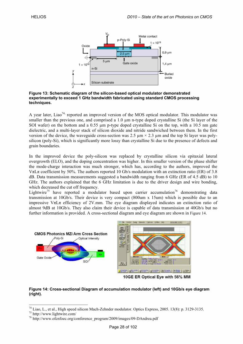
HELIOS D010 – State of the art on Photonics on CMOS
Page 28 of 102
Figure 13: Schematic diagram of the silicon-based optical modulator demonstrated experimentally to exceed 1 GHz bandwidth fabricated using standard CMOS processing techniques.
A year later, Liao74, reported an improved version of the MOS optical modulator. This modulator was smaller than the previous one, and comprised a 1.0 µm n-type doped crystalline Si (the Si layer of the SOI wafer) on the bottom and a 0.55 µm p-type doped crystalline Si on the top, with a 10.5 nm gate dielectric, and a multi-layer stack of silicon dioxide and nitride sandwiched between them. In the first version of the device, the waveguide cross-section was 2.5 µm × 2.3 µm and the top Si layer was poly-silicon (poly-Si), which is significantly more lossy than crystalline Si due to the presence of defects and grain boundaries. In the improved device the poly-silicon was replaced by crystalline silicon via epitaxial lateral overgrowth (ELO), and the doping concentration was higher. In this smaller version of the phase shifter the mode-charge interaction was much stronger, which has, according to the authors, improved the VπLπ coefficient by 50%. The authors reported 10 Gb/s modulation with an extinction ratio (ER) of 3.8 dB. Data transmission measurements suggested a bandwidth ranging from 6 GHz (ER of 4.5 dB) to 10 GHz. The authors explained that the 6 GHz limitation is due to the driver design and wire bonding, which decreased the cut off frequency. Lightwire75 have reported a modulator based upon carrier accumulation76 demonstrating data transmission at 10Gb/s. Their device is very compact (800um x 15um) which is possible due to an impressive VπLπ efficiency of 2V.mm. The eye diagram displayed indicates an extinction ratio of almost 9dB at 10Gb/s. They also claim their device is capable of data transmission at 40Gb/s but no further information is provided. A cross-sectional diagram and eye diagram are shown in Figure 14.
Figure 14: Cross-sectional Diagram of accumulation modulator (left) and 10Gb/s eye diagram (right).
74 Liao, L., et al., High speed silicon Mach-Zehnder modulator. Optics Express, 2005. 13(8): p. 3129-3135. 75 http://www.lightwire.com/ 76 http://www.ofcnfoec.org/conference_program/2009/images/09-DAndrea.pdf
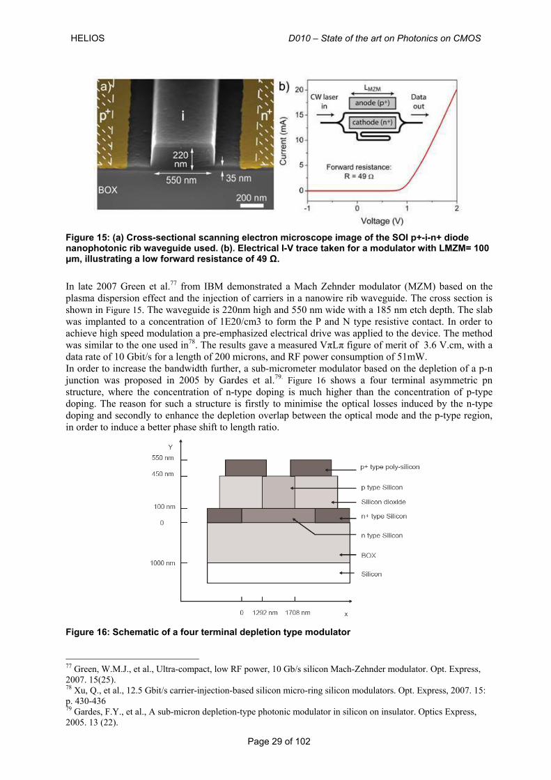
HELIOS D010 – State of the art on Photonics on CMOS
Page 29 of 102
Figure 15: (a) Cross-sectional scanning electron microscope image of the SOI p+-i-n+ diode nanophotonic rib waveguide used. (b). Electrical I-V trace taken for a modulator with LMZM= 100 μm, illustrating a low forward resistance of 49 Ω.
In late 2007 Green et al.77 from IBM demonstrated a Mach Zehnder modulator (MZM) based on the plasma dispersion effect and the injection of carriers in a nanowire rib waveguide. The cross section is shown in Figure 15. The waveguide is 220nm high and 550 nm wide with a 185 nm etch depth. The slab was implanted to a concentration of 1E20/cm3 to form the P and N type resistive contact. In order to achieve high speed modulation a pre-emphasized electrical drive was applied to the device. The method was similar to the one used in78. The results gave a measured VπLπ figure of merit of 3.6 V.cm, with a data rate of 10 Gbit/s for a length of 200 microns, and RF power consumption of 51mW. In order to increase the bandwidth further, a sub-micrometer modulator based on the depletion of a p-n junction was proposed in 2005 by Gardes et al.79. Figure 16 shows a four terminal asymmetric pn structure, where the concentration of n-type doping is much higher than the concentration of p-type doping. The reason for such a structure is firstly to minimise the optical losses induced by the n-type doping and secondly to enhance the depletion overlap between the optical mode and the p-type region, in order to induce a better phase shift to length ratio.
Figure 16: Schematic of a four terminal depletion type modulator
77 Green, W.M.J., et al., Ultra-compact, low RF power, 10 Gb/s silicon Mach-Zehnder modulator. Opt. Express, 2007. 15(25). 78 Xu, Q., et al., 12.5 Gbit/s carrier-injection-based silicon micro-ring silicon modulators. Opt. Express, 2007. 15: p. 430-436 79 Gardes, F.Y., et al., A sub-micron depletion-type photonic modulator in silicon on insulator. Optics Express, 2005. 13 (22).
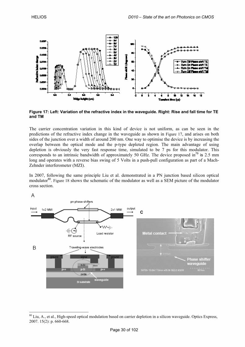
HELIOS D010 – State of the art on Photonics on CMOS
Page 30 of 102
Figure 17: Left: Variation of the refractive index in the waveguide. Right: Rise and fall time for TE and TM
The carrier concentration variation in this kind of device is not uniform, as can be seen in the predictions of the refractive index change in the waveguide as shown in Figure 17, and arises on both sides of the junction over a width of around 200 nm. One way to optimise the device is by increasing the overlap between the optical mode and the p-type depleted region. The main advantage of using depletion is obviously the very fast response time, simulated to be 7 ps for this modulator. This corresponds to an intrinsic bandwidth of approximately 50 GHz. The device proposed in79 is 2.5 mm long and operates with a reverse bias swing of 5 Volts in a push-pull configuration as part of a Mach- Zehnder interferometer (MZI). In 2007, following the same principle Liu et al. demonstrated in a PN junction based silicon optical modulator80. Figure 18 shows the schematic of the modulator as well as a SEM picture of the modulator cross section.
C
80 Liu, A., et al., High-speed optical modulation based on carrier depletion in a silicon waveguide. Optics Express, 2007. 15(2): p. 660-668.
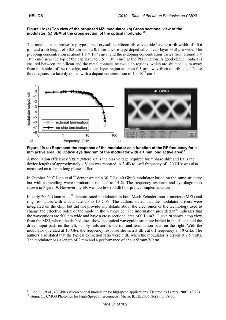
HELIOS D010 – State of the art on Photonics on CMOS
Page 31 of 102
Figure 18: (a) Top view of the proposed MZI modulator. (b) Cross sectional view of the modulator. (c) SEM of the cross section of the optical modulator80.
The modulator comprises a p-type doped crystalline silicon rib waveguide having a rib width of ~0.6 µm and a rib height of ~0.5 µm with a 0.1 µm thick n-type doped silicon cap layer ~1.8 µm wide. The p-doping concentration is about 1.5 × 1017 cm-3, and the n-doping concentration varies from around 3 × 1018 cm-3 near the top of the cap layer to 1.5 × 1017 cm-3 at the PN junction. A good ohmic contact is ensured between the silicon and the metal contacts by two slab regions, which are situated 1 µm away from both sides of the rib edge, and a cap layer region at about 0.3 µm away from the rib edge. Those three regions are heavily doped with a dopant concentration of 1 × 1020 cm-3.
Figure 19: (a) Represent the response of the modulator as a function of the RF frequency for a 1 mm active area. (b) Optical eye diagram of the modulator with a 1 mm long active area81.
A modulation efficiency VπLπ (where Vπ is the bias voltage required for π phase shift and Lπ is the device length) of approximately 4 V.cm was reported. A 3-dB roll-off frequency of ~20 GHz was also measured on a 1 mm long phase shifter. In October 2007 Liao et al.81 demonstrated a 30 GHz, 40 Gbit/s modulator based on the same structure but with a travelling wave termination reduced to 14 Ω. The frequency response and eye diagram is shown in Figure 19. However the ER was too low (0.5dB) for pratical implementation In early 2006, Gunn et al.82 demonstrated modulation in both Mach Zehnder interferometers (MZI) and ring resonators with a data rate up to 10 Gb/s. The authors stated that the modulator drivers were integrated on the chip, but did not provide any details about the electronics or the technology used to change the effective index of the mode in the waveguide. The information provided in82 indicates that the waveguides are 500 nm wide and have a cross sectional area of 0.1 μm2. Figure 20 shows a top view from the MZI, where the dashed lines show the optical waveguide structure buried in the silicon and the driver input pads on the left, supply rails across the top and termination pads on the right. With the modulator operated at 10 Gb/s the frequency response shows a 3 dB cut off frequency at 10 GHz. The authors also stated that the typical extinction ratio were 5 dB when the modulator is driven at 2.5 Volts. The modulator has a length of 2 mm and a performance of about 5°/mm/V/arm.
81 Liao, L., et al., 40 Gbit/s silicon optical modulator for highspeed applications. Electronics Letters, 2007. 43(22). 82 Gunn, C., CMOS Photonics for High-Speed Interconnects. Micro, IEEE, 2006. 26(2): p. 58-66.
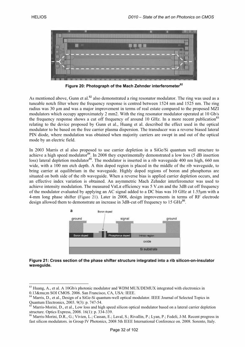
HELIOS D010 – State of the art on Photonics on CMOS
Page 32 of 102
Figure 20: Photograph of the Mach Zehnder interferometer82
As mentioned above, Gunn et al.82 also demonstrated a ring resonator modulator. The ring was used as a tuneable notch filter where the frequency response is centred between 1524 nm and 1525 nm. The ring radius was 30 µm and was a major improvement in terms of real estate compared to the proposed MZI modulators which occupy approximately 2 mm2. With the ring resonator modulator operated at 10 Gb/s the frequency response shows a cut off frequency of around 10 GHz. In a more recent publication83 relating to the device proposed by Gunn et al., Huang et al. described the effect used in the optical modulator to be based on the free carrier plasma dispersion. The transducer was a reverse biased lateral PIN diode, where modulation was obtained when majority carriers are swept in and out of the optical mode by an electric field. In 2003 Marris et al also proposed to use carrier depletion in a SiGe/Si quantum well structure to achieve a high speed modulator84. In 2008 they experimentally demonstrated a low loss (5 dB insertion loss) lateral depletion modulator85. The modulator is inserted in a rib waveguide 400 nm high, 660 nm wide, with a 100 nm etch depth. A thin doped region is placed in the middle of the rib waveguide, to bring carrier at equilibrium in the waveguide. Highly doped regions of boron and phosphorus are situated on both side of the rib waveguide. When a reverse bias is applied carrier depletion occurs, and an effective index variation is obtained. An asymmetric Mach Zehnder interferometer was used to achieve intensity modulation. The measured VπLπ efficiency was 5 V.cm and the 3dB cut off frequency of the modulator evaluated by applying an AC signal added to a DC bias was 10 GHz at 1.55μm with a 4-mm long phase shifter (Figure 21). Later in 2008, design improvements in terms of RF electrode design allowed them to demonstrate an increase in 3dB-cut off frequency to 15 GHz86.
Figure 21: Cross section of the phase shifter structure integrated into a rib silicon-on-insulator waveguide.
83 Huang, A., et al. A 10Gb/s photonic modulator and WDM MUX/DEMUX integrated with electronics in 0.13μm SOI CMOS. 2006. San Francisco, CA, USA: IEEE. 84 Marris, D., et al., Design of a SiGe-Si quantum-well optical modulator. IEEE Journal of Selected Topics in Quantum Electronics, 2003. 9(3): p. 747-54. 85 Marris-Morini, D., et al., Low loss and high speed silicon optical modulator based on a lateral carrier depletion structure. Optics Express, 2008. 16(1): p. 334-339. 86 Marris-Morini, D.R., G.; Vivien, L.; Cassan, E.; Laval, S.; Rivallin, P.; Lyan, P.; Fedeli, J-M. Recent progress in fast silicon modulators. in Group IV Photonics, 2008 5th IEEE International Conference on. 2008. Sorento, Italy.
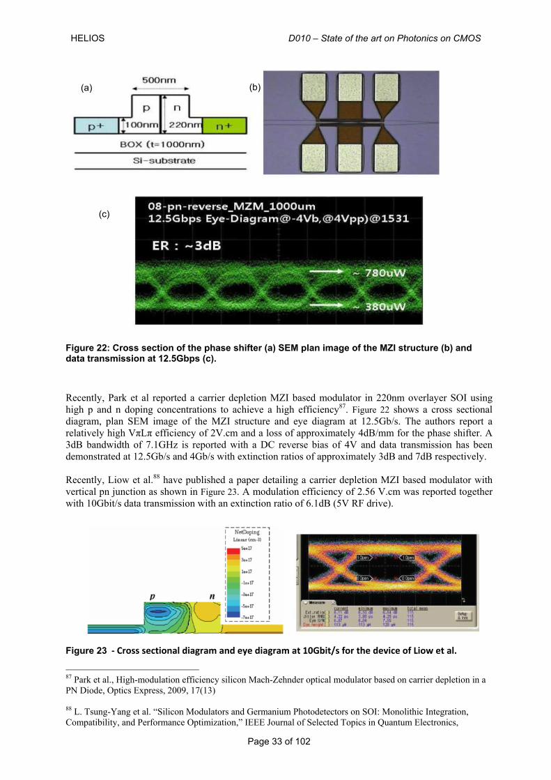
HELIOS D010 – State of the art on Photonics on CMOS
Page 33 of 102
Figure 22: Cross section of the phase shifter (a) SEM plan image of the MZI structure (b) and data transmission at 12.5Gbps (c).
Recently, Park et al reported a carrier depletion MZI based modulator in 220nm overlayer SOI using high p and n doping concentrations to achieve a high efficiency87. Figure 22 shows a cross sectional diagram, plan SEM image of the MZI structure and eye diagram at 12.5Gb/s. The authors report a relatively high VπLπ efficiency of 2V.cm and a loss of approximately 4dB/mm for the phase shifter. A 3dB bandwidth of 7.1GHz is reported with a DC reverse bias of 4V and data transmission has been demonstrated at 12.5Gb/s and 4Gb/s with extinction ratios of approximately 3dB and 7dB respectively. Recently, Liow et al.88 have published a paper detailing a carrier depletion MZI based modulator with vertical pn junction as shown in Figure 23. A modulation efficiency of 2.56 V.cm was reported together with 10Gbit/s data transmission with an extinction ratio of 6.1dB (5V RF drive).
Figure 23 ‐ Cross sectional diagram and eye diagram at 10Gbit/s for the device of Liow et al.
87 Park et al., High-modulation efficiency silicon Mach-Zehnder optical modulator based on carrier depletion in a PN Diode, Optics Express, 2009, 17(13) 88 L. Tsung-Yang et al. “Silicon Modulators and Germanium Photodetectors on SOI: Monolithic Integration, Compatibility, and Performance Optimization,” IEEE Journal of Selected Topics in Quantum Electronics,
(a) (b)
(c)
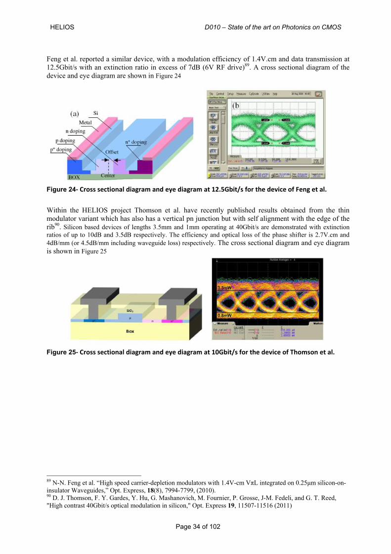
HELIOS D010 – State of the art on Photonics on CMOS
Page 34 of 102
Feng et al. reported a similar device, with a modulation efficiency of 1.4V.cm and data transmission at 12.5Gbit/s with an extinction ratio in excess of 7dB (6V RF drive)89. A cross sectional diagram of the device and eye diagram are shown in Figure 24
Figure 24‐ Cross sectional diagram and eye diagram at 12.5Gbit/s for the device of Feng et al.
Within the HELIOS project Thomson et al. have recently published results obtained from the thin modulator variant which has also has a vertical pn junction but with self alignment with the edge of the rib90. Silicon based devices of lengths 3.5mm and 1mm operating at 40Gbit/s are demonstrated with extinction ratios of up to 10dB and 3.5dB respectively. The efficiency and optical loss of the phase shifter is 2.7V.cm and 4dB/mm (or 4.5dB/mm including waveguide loss) respectively. The cross sectional diagram and eye diagram is shown in Figure 25
Figure 25‐ Cross sectional diagram and eye diagram at 10Gbit/s for the device of Thomson et al.
89 N-N. Feng et al. “High speed carrier-depletion modulators with 1.4V-cm VπL integrated on 0.25μm silicon-on-insulator Waveguides,” Opt. Express, 18(8), 7994-7799, (2010). 90 D. J. Thomson, F. Y. Gardes, Y. Hu, G. Mashanovich, M. Fournier, P. Grosse, J-M. Fedeli, and G. T. Reed, "High contrast 40Gbit/s optical modulation in silicon," Opt. Express 19, 11507-11516 (2011)
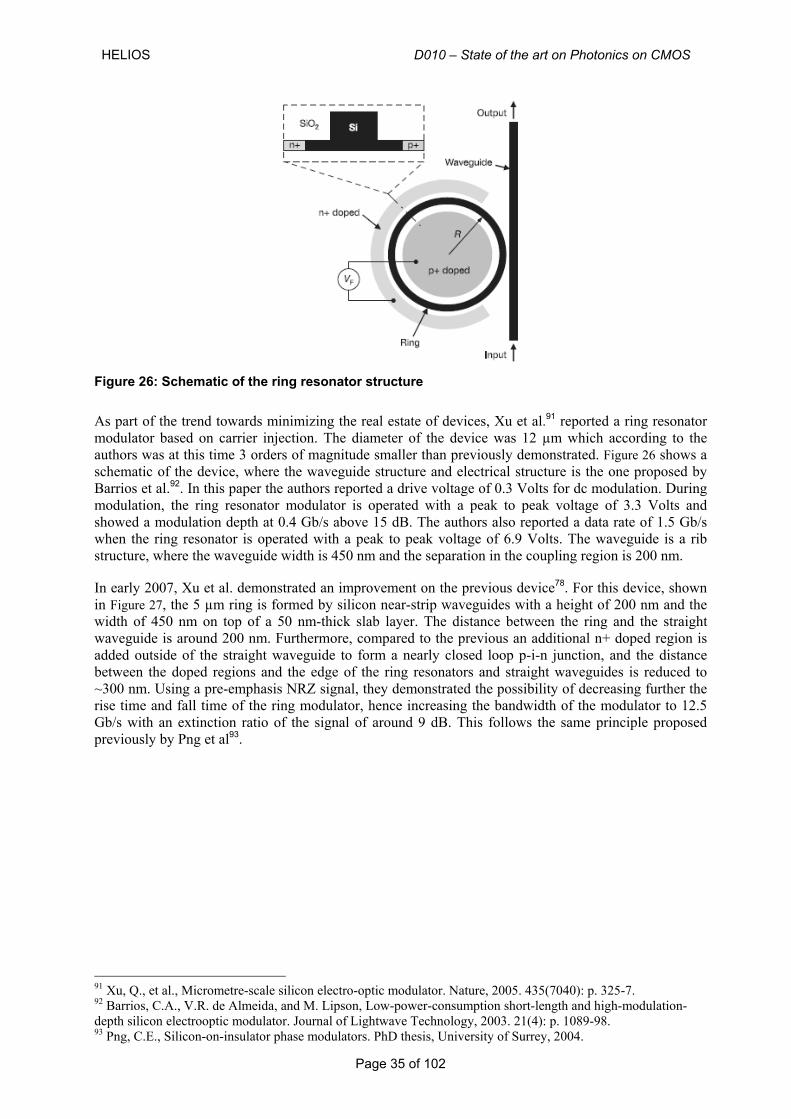
HELIOS D010 – State of the art on Photonics on CMOS
Page 35 of 102
Figure 26: Schematic of the ring resonator structure As part of the trend towards minimizing the real estate of devices, Xu et al.91 reported a ring resonator modulator based on carrier injection. The diameter of the device was 12 µm which according to the authors was at this time 3 orders of magnitude smaller than previously demonstrated. Figure 26 shows a schematic of the device, where the waveguide structure and electrical structure is the one proposed by Barrios et al.92. In this paper the authors reported a drive voltage of 0.3 Volts for dc modulation. During modulation, the ring resonator modulator is operated with a peak to peak voltage of 3.3 Volts and showed a modulation depth at 0.4 Gb/s above 15 dB. The authors also reported a data rate of 1.5 Gb/s when the ring resonator is operated with a peak to peak voltage of 6.9 Volts. The waveguide is a rib structure, where the waveguide width is 450 nm and the separation in the coupling region is 200 nm. In early 2007, Xu et al. demonstrated an improvement on the previous device78. For this device, shown in Figure 27, the 5 µm ring is formed by silicon near-strip waveguides with a height of 200 nm and the width of 450 nm on top of a 50 nm-thick slab layer. The distance between the ring and the straight waveguide is around 200 nm. Furthermore, compared to the previous an additional n+ doped region is added outside of the straight waveguide to form a nearly closed loop p-i-n junction, and the distance between the doped regions and the edge of the ring resonators and straight waveguides is reduced to ~300 nm. Using a pre-emphasis NRZ signal, they demonstrated the possibility of decreasing further the rise time and fall time of the ring modulator, hence increasing the bandwidth of the modulator to 12.5 Gb/s with an extinction ratio of the signal of around 9 dB. This follows the same principle proposed previously by Png et al93.
91 Xu, Q., et al., Micrometre-scale silicon electro-optic modulator. Nature, 2005. 435(7040): p. 325-7. 92 Barrios, C.A., V.R. de Almeida, and M. Lipson, Low-power-consumption short-length and high-modulation-depth silicon electrooptic modulator. Journal of Lightwave Technology, 2003. 21(4): p. 1089-98. 93 Png, C.E., Silicon-on-insulator phase modulators. PhD thesis, University of Surrey, 2004.
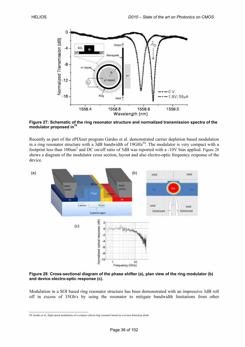
HELIOS D010 – State of the art on Photonics on CMOS
Page 36 of 102
Figure 27: Schematic of the ring resonator structure and normalized transmission spectra of the modulator proposed in78
Recently as part of the ePIXnet program Gardes et al. demonstrated carrier depletion based modulation in a ring resonator structure with a 3dB bandwidth of 19GHz94. The modulator is very compact with a footprint less than 100um2 and DC on/off ratio of 5dB was reported with a -10V bias applied. Figure 28 shows a diagram of the modulator cross section, layout and also electro-optic frequency response of the device.
Figure 28: Cross-sectional diagram of the phase shifter (a), plan view of the ring modulator (b) and device electro-optic response (c).
Modulation in a SOI based ring resonator structure has been demonstrated with an impressive 3dB roll off in excess of 35Gb/s by using the resonator to mitigate bandwidth limitations from other
94 Gardes et al., High-speed modulation of a compact silicon ring resonator based on a reverse-biased pn diode
(a) (b)
(c)
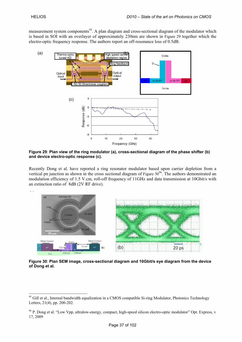
HELIOS D010 – State of the art on Photonics on CMOS
Page 37 of 102
measurement system components95. A plan diagram and cross-sectional diagram of the modulator which is based in SOI with an overlayer of approximately 230nm are shown in Figure 29 together which the electro-optic frequency response. The authors report an off-resonance loss of 0.5dB.
Figure 29: Plan view of the ring modulator (a), cross-sectional diagram of the phase shifter (b) and device electro-optic response (c).
Recently Dong et al. have reported a ring resonator modulator based upon carrier depletion from a vertical pn junction as shown in the cross sectional diagram of Figure 3096. The authors demonstrated an modulation efficiency of 1.5 V.cm, roll-off frequency of 11GHz and data transmission at 10Gbit/s with an extinction ratio of 8dB (2V RF drive).
Figure 30: Plan SEM image, cross-sectional diagram and 10Gbit/s eye diagram from the device of Dong et al.
95 Gill et al., Internal bandwidth equalization in a CMOS compatible Si-ring Modulator, Photonics Technology Letters, 21(4), pp. 200-202. 96 P. Dong et al. “Low Vpp, ultralow-energy, compact, high-speed silicon electro-optic modulator” Opt. Express, v 17, 2009
(a) (b)
(c)
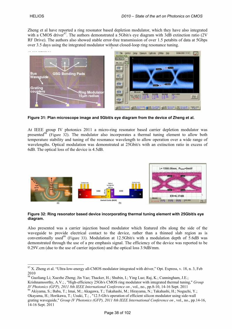
HELIOS D010 – State of the art on Photonics on CMOS
Page 38 of 102
Zheng et al have reported a ring resonator based depletion modulator, which they have also integrated with a CMOS driver97. The authors demonstrated a 5Gbit/s eye diagram with 3dB extinction ratio (2V RF Drive). The authors also showed stable error-free transmission of over 1.5 petabits of data at 5Gbps over 3.5 days using the integrated modulator without closed-loop ring resonance tuning.
Figure 31: Plan microscope image and 5Gbit/s eye diagram from the device of Zheng et al.
At IEEE group IV photonics 2011 a micro-ring resonator based carrier depletion modulator was presented98 (Figure 32). The modulator also incorporates a thermal tuning element to allow both temperature stability and tuning of the resonance wavelength to allow operation over a wide range of wavelengths. Optical modulation was demonstrated at 25Gbit/s with an extinction ratio in excess of 6dB. The optical loss of the device is 4.5dB.
Figure 32: Ring resonator based device incorporating thermal tuning element with 25Gbit/s eye diagram.
Also presented was a carrier injection based modulator which featured ribs along the side of the waveguide to provide electrical contact to the device, rather than a thinned slab region as is conventionally used99 (Figure 33). Modulation at 12.5Gbit/s with a modulation depth of 5.6dB was demonstrated through the use of a pre emphasis signal. The efficiency of the device was reported to be 0.29V.cm (due to the use of carrier injection) and the optical loss 3.9dB/mm.
97 X. Zheng et al. “Ultra-low-energy all-CMOS modulator integrated with driver,” Opt. Express, v. 18, n. 3, Feb 2010 98 Guoliang Li; Xuezhe Zheng; Jin Yao; Thacker, H.; Shubin, I.; Ying Luo; Raj, K.; Cunningham, J.E.; Krishnamoorthy, A.V.; , "High-efficiency 25Gb/s CMOS ring modulator with integrated thermal tuning," Group IV Photonics (GFP), 2011 8th IEEE International Conference on , vol., no., pp.8-10, 14-16 Sept. 2011 99 Akiyama, S.; Baba, T.; Imai, M.; Akagawa, T.; Takahashi, M.; Hirayama, N.; Takahashi, H.; Noguchi, Y.; Okayama, H.; Horikawa, T.; Usuki, T.; , "12.5-Gb/s operation of efficient silicon modulator using side-wall grating waveguide," Group IV Photonics (GFP), 2011 8th IEEE International Conference on , vol., no., pp.14-16, 14-16 Sept. 2011
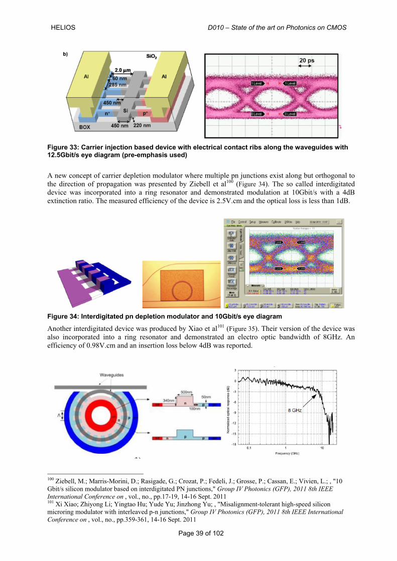
HELIOS D010 – State of the art on Photonics on CMOS
Page 39 of 102
Figure 33: Carrier injection based device with electrical contact ribs along the waveguides with 12.5Gbit/s eye diagram (pre-emphasis used)
A new concept of carrier depletion modulator where multiple pn junctions exist along but orthogonal to the direction of propagation was presented by Ziebell et al100 (Figure 34). The so called interdigitated device was incorporated into a ring resonator and demonstrated modulation at 10Gbit/s with a 4dB extinction ratio. The measured efficiency of the device is 2.5V.cm and the optical loss is less than 1dB.
Figure 34: Interdigitated pn depletion modulator and 10Gbit/s eye diagram
Another interdigitated device was produced by Xiao et al101 (Figure 35). Their version of the device was also incorporated into a ring resonator and demonstrated an electro optic bandwidth of 8GHz. An efficiency of 0.98V.cm and an insertion loss below 4dB was reported.
100 Ziebell, M.; Marris-Morini, D.; Rasigade, G.; Crozat, P.; Fedeli, J.; Grosse, P.; Cassan, E.; Vivien, L.; , "10 Gbit/s silicon modulator based on interdigitated PN junctions," Group IV Photonics (GFP), 2011 8th IEEE International Conference on , vol., no., pp.17-19, 14-16 Sept. 2011 101 Xi Xiao; Zhiyong Li; Yingtao Hu; Yude Yu; Jinzhong Yu; , "Misalignment-tolerant high-speed silicon microring modulator with interleaved p-n junctions," Group IV Photonics (GFP), 2011 8th IEEE International Conference on , vol., no., pp.359-361, 14-16 Sept. 2011
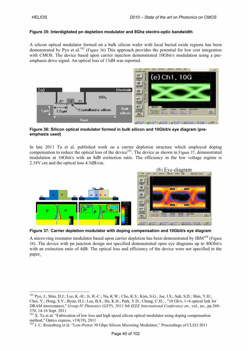
HELIOS D010 – State of the art on Photonics on CMOS
Page 40 of 102
Figure 35: Interdigitated pn depletion modulator and 8Ghz electro-optic bandwidth
A silicon optical modulator formed on a bulk silicon wafer with local buried oxide regions has been demonstrated by Pyo et al.102 (Figure 36) This approach provides the potential for low cost integration with CMOS. The device based upon carrier injection demonstrated 10Gbit/s modulation using a pre-emphasis drive signal. An optical loss of 13dB was reported.
Figure 36: Silicon optical modulator formed in bulk silicon and 10Gbit/s eye diagram (pre-emphasis used)
In late 2011 Tu et al. published work on a carrier depletion structure which employed doping compensation to reduce the optical loss of the device103. The device as shown in Figure 37, demonstrated modulation at 10Gbit/s with an 8dB extinction ratio. The efficiency in the low voltage regime is 2.18V.cm and the optical loss 4.5dB/cm.
Figure 37: Carrier depletion modulator with doping compensation and 10Gbit/s eye diagram
A micro-ring resonator modulator based upon carrier depletion has been demonstrated by IBM104 (Figure 38). The device with pn junction design not specified demonstrated open eye diagrams up to 40Gbit/s with an extinction ratio of 4dB. The optical loss and efficiency of the device were not specified in the paper.
102 Pyo, J.; Shin, D.J.; Lee, K.-H.; Ji, H.-C.; Na, K.W.; Cho, K.S.; Kim, S.G.; Joe, I.S.; Suh, S.D.; Shin, Y.H.; Choi, Y.; Hong, S.Y.; Byun, H.I.; Lee, B.S.; Ha, K.H.; Park, Y.D.; Chung, C.H.; , "10 Gb/s, 1×4 optical link for DRAM interconnect," Group IV Photonics (GFP), 2011 8th IEEE International Conference on , vol., no., pp.368-370, 14-16 Sept. 2011 103 X. Tu et al. “Fabrication of low loss and high speed silicon optical modulator using doping compensation method,” Optics express, v19(19), 2011 104 J. C. Rosenberg et al. “Low-Power 30 Gbps Silicon Microring Modulator,” Proceedings of CLEO 2011
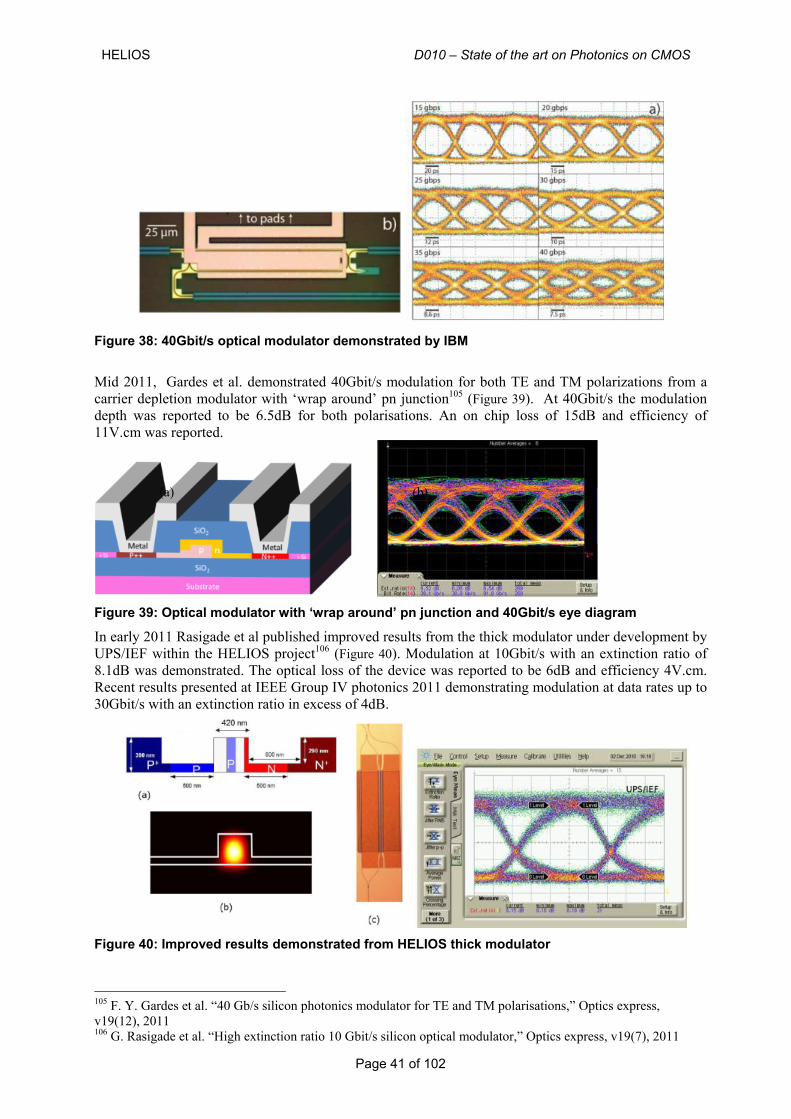
HELIOS D010 – State of the art on Photonics on CMOS
Page 41 of 102
Figure 38: 40Gbit/s optical modulator demonstrated by IBM Mid 2011, Gardes et al. demonstrated 40Gbit/s modulation for both TE and TM polarizations from a carrier depletion modulator with ‘wrap around’ pn junction105 (Figure 39). At 40Gbit/s the modulation depth was reported to be 6.5dB for both polarisations. An on chip loss of 15dB and efficiency of 11V.cm was reported.
Figure 39: Optical modulator with ‘wrap around’ pn junction and 40Gbit/s eye diagram
In early 2011 Rasigade et al published improved results from the thick modulator under development by UPS/IEF within the HELIOS project106 (Figure 40). Modulation at 10Gbit/s with an extinction ratio of 8.1dB was demonstrated. The optical loss of the device was reported to be 6dB and efficiency 4V.cm. Recent results presented at IEEE Group IV photonics 2011 demonstrating modulation at data rates up to 30Gbit/s with an extinction ratio in excess of 4dB.
Figure 40: Improved results demonstrated from HELIOS thick modulator 105 F. Y. Gardes et al. “40 Gb/s silicon photonics modulator for TE and TM polarisations,” Optics express, v19(12), 2011 106 G. Rasigade et al. “High extinction ratio 10 Gbit/s silicon optical modulator,” Optics express, v19(7), 2011
(a) (b)
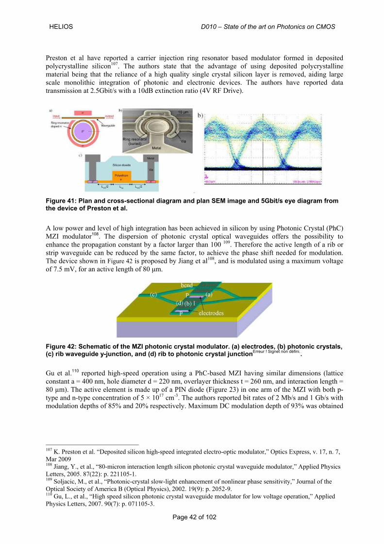
HELIOS D010 – State of the art on Photonics on CMOS
Page 42 of 102
Preston et al have reported a carrier injection ring resonator based modulator formed in deposited polycrystalline silicon107. The authors state that the advantage of using deposited polycrystalline material being that the reliance of a high quality single crystal silicon layer is removed, aiding large scale monolithic integration of photonic and electronic devices. The authors have reported data transmission at 2.5Gbit/s with a 10dB extinction ratio (4V RF Drive).
Figure 41: Plan and cross-sectional diagram and plan SEM image and 5Gbit/s eye diagram from the device of Preston et al.
A low power and level of high integration has been achieved in silicon by using Photonic Crystal (PhC) MZI modulator108. The dispersion of photonic crystal optical waveguides offers the possibility to enhance the propagation constant by a factor larger than 100 109. Therefore the active length of a rib or strip waveguide can be reduced by the same factor, to achieve the phase shift needed for modulation. The device shown in Figure 42 is proposed by Jiang et al108, and is modulated using a maximum voltage of 7.5 mV, for an active length of 80 μm.
Figure 42: Schematic of the MZI photonic crystal modulator. (a) electrodes, (b) photonic crystals, (c) rib waveguide y-junction, and (d) rib to photonic crystal junctionErreur ! Signet non défini..
Gu et al.110 reported high-speed operation using a PhC-based MZI having similar dimensions (lattice constant a = 400 nm, hole diameter d = 220 nm, overlayer thickness t = 260 nm, and interaction length = 80 µm). The active element is made up of a PIN diode (Figure 23) in one arm of the MZI with both p-type and n-type concentration of 5 × 1017 cm-3. The authors reported bit rates of 2 Mb/s and 1 Gb/s with modulation depths of 85% and 20% respectively. Maximum DC modulation depth of 93% was obtained
107 K. Preston et al. “Deposited silicon high-speed integrated electro-optic modulator,” Optics Express, v. 17, n. 7, Mar 2009 108 Jiang, Y., et al., “80-micron interaction length silicon photonic crystal waveguide modulator,” Applied Physics Letters, 2005. 87(22): p. 221105-1. 109 Soljacic, M., et al., “Photonic-crystal slow-light enhancement of nonlinear phase sensitivity,” Journal of the Optical Society of America B (Optical Physics), 2002. 19(9): p. 2052-9. 110 Gu, L., et al., “High speed silicon photonic crystal waveguide modulator for low voltage operation,” Applied Physics Letters, 2007. 90(7): p. 071105-3.
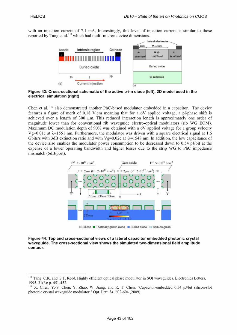
HELIOS D010 – State of the art on Photonics on CMOS
Page 43 of 102
with an injection current of 7.1 mA. Interestingly, this level of injection current is similar to those reported by Tang et al.111 which had multi-micron device dimensions.
Figure 43: Cross-sectional schematic of the active p-i-n diode (left), 2D model used in the electrical simulation (right)
Chen et al. 112 also demonstrated another PhC-based modulator embedded in a capacitor. The device features a figure of merit of 0.18 V.cm meaning that for a 6V applied voltage, a pi-phase shift is achieved over a length of 300 µm. This reduced interaction length is approximately one order of magnitude lower than for conventional rib waveguide electro-optical modulators (rib WG EOM). Maximum DC modulation depth of 90% was obtained with a 6V applied voltage for a group velocity Vg=0.01c at λ=1551 nm. Furthermore, the modulator was driven with a square electrical signal at 1.6 Gbits/s with 3dB extinction ratio and with Vg=0.02c at λ=1548 nm. In addition, the low capacitance of the device also enables the modulator power consumption to be decreased down to 0.54 pJ/bit at the expense of a lower operating bandwidth and higher losses due to the strip WG to PhC impedance mismatch (5dB/port).
Figure 44: Top and cross-sectional views of a lateral capacitor embedded photonic crystal waveguide. The cross-sectional view shows the simulated two-dimensional field amplitude contour.
111 Tang, C.K. and G.T. Reed, Highly efficient optical phase modulator in SOI waveguides. Electronics Letters, 1995. 31(6): p. 451-452. 112 X. Chen, Y.-S. Chen, Y. Zhao, W. Jiang, and R. T. Chen, "Capacitor-embedded 0.54 pJ/bit silicon-slot photonic crystal waveguide modulator," Opt. Lett. 34, 602-604 (2009).
HELIOS D010 – State of the art on Photonics on CMOS
Page 44 of 102
In an effort to increase the slow wave modulator optical bandwidth, S. Akiyama 113 et al reported a slow-light Mach-Zehnder modulator with cascaded ring resonators. The fabricated device operates at 10 Gb/s in the free carrier injection regime with pre-emphasis with a driving voltage of 1 Vpp over a wavelength range of 1 nm (1551-1552nm) and without any adjustment of the resonant wavelengths (no thermal DC tuning). The extinction ratio lies between 3 and 5dB over the same bandwidth. The MZI arm length is 478 µm. Compared to a conventional MZI (i.e. not ring-loaded) the injection current (4.21 A) is decreased by a factor lying between 4 and 9: 0.86, 0.45 and 1.05 at 1551.0, 1551.5, and 1552.0 nm, respectively.
Figure 45: (a) Conceptual drawing of proposed resonator-based silicon modulator integrated with laser source. The bottom photograph shows fabricated RRloaded MZ modulator, which is presented in this paper. (b) Cross section of the RR loaded on MZI on the dotted line as in (a).
Silicon has been limited as an optical material for decades because of a lack of or limited active optical properties. In a paper published in 2006, Jacobsen et al demonstrated a significant linear electro optic effect induced in silicon by breaking the crystal symmetry. The inversion symmetry of silicon crystal prohibits the existence of a linear electro optic effect; hence by applying an asymmetric strain on the waveguide, the symmetry can be broken. Figure 46 shows the principle used for the proposed device, where a straining layer is deposited on the top of the waveguide. The proposed structure used a deposited silicon nitride glass layer (Si3N4) as a straining layer114. The amorphous Si3N4 is pre-compressively strained and hence tries to expand the structure underneath in both horizontal directions, hence creating the asymmetry.
Figure 46 : Applying strain to crystalline silicon. (a) Waveguide fabricated in the top layer of an SOI wafer, (b) The same waveguide with a straining layer deposited on top. The straining layer breaks the inversion symmetry and induces a linear electro-optic effect68.
113 S. Akiyama, T. Kurahashi, T. Baba, N. Hatori, T. Usuki, and T. Yamamoto1 "1-Vpp 10-Gb/s Operation of Slow-Light Silicon Mach-Zehnder Modulator in Wavelength Range of 1 nm" Proceedings Group IV Photonic conference, p. 45-47 (2010) 114 Madou, J.M., Fundamentals of Microfabrication. Boca Raton ed. 2002, Florida: CRC press.
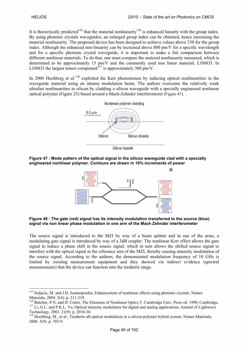
HELIOS D010 – State of the art on Photonics on CMOS
Page 45 of 102
It is theoretically predicted115 that the material nonlinearity116 is enhanced linearly with the group index. By using photonic crystals waveguides, an enlarged group index can be obtained, hence increasing the material nonlinearity. The proposed device has been designed to achieve values above 230 for the group index. Although the enhanced non-linearity can be increased above 800 pm/V for a specific wavelength and for a specific photonic crystal waveguide, it is important to make a fair comparison between different nonlinear materials. To do that, one must compare the material nonlinearity measured, which is determined to be approximately 15 pm/V and the commonly used non linear material, LiNbO3. In LiNbO3 the largest tensor component117 is approximately 360 pm/V. In 2006 Hochberg et al.118 exploited the Kerr phenomenon by inducing optical nonlinearities in the waveguide material using an intense modulation beam. The authors overcame the relatively weak ultrafast nonlinearities in silicon by cladding a silicon waveguide with a specially engineered nonlinear optical polymer (Figure 25) based around a Mach-Zehnder interferometer (Figure 47).
Figure 47 : Mode pattern of the optical signal in the silicon waveguide clad with a specially engineered nonlinear polymer. Contours are drawn in 10% increments of power
Figure 48 : The gate (red) signal has its intensity modulation transferred to the source (blue) signal via non linear phase modulation in one arm of the Mach Zehnder interferometer
The source signal is introduced to the MZI by way of a beam splitter and in one of the arms, a modulating gate signal is introduced by way of a 3dB coupler. The nonlinear Kerr effect allows the gate signal to induce a phase shift in the source signal, which in turn allows the shifted source signal to interfere with the optical signal in the reference arm of the MZI, thereby causing intensity modulation of the source signal. According to the authors, the demonstrated modulation frequency of 10 GHz is limited by existing measurement equipment and they showed via indirect evidence (spectral measurements) that the device can function into the terahertz range.
115 Soljacic, M. and J.D. Joannopoulos, Enhancement of nonlinear effects using photonic crystals. Nature Materials, 2004. 3(4): p. 211-219. 116 Butcher, P.N. and D. Cotter, The Elements of Nonlinear Optics 5. Cambridge Univ. Press ed. 1990, Cambridge. 117 Li, G.L. and P.K.L. Yu, Optical intensity modulators for digital and analog applications. Journal of Lightwave Technology, 2003. 21(9): p. 2010-30. 118 Hochberg, M., et al., Terahertz all-optical modulation in a silicon-polymer hybrid system. Nature Materials, 2006. 5(9): p. 703-9.
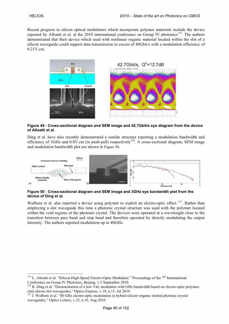
HELIOS D010 – State of the art on Photonics on CMOS
Page 46 of 102
Recent progress in silicon optical modulators which incorporate polymer materials include the device reported by Alloatti et al. at the 2010 international conference on Group IV photonics119. The authors demonstrated that their device which used with nonlinear organic material located within the slot of a silicon waveguide could support data transmission in excess of 40Gbit/s with a modulation efficiency of 0.21V.cm.
Figure 49 : Cross-sectional diagram and SEM image and 42.7Gbit/s eye diagram from the device of Alloatti et al.
Ding et al. have also recently demonstrated a similar structure reporting a modulation bandwidth and efficiency of 3GHz and 0.8V.cm (in push-pull) respectively120. A cross-sectional diagram, SEM image and modulation bandwidth plot are shown in Figure 50.
Figure 50 : Cross-sectional diagram and SEM image and 3GHz eye bandwidth plot from the device of Ding et al.
Wulburn et al. also reported a device using polymer to exploit an electro-optic effect 121. Rather than employing a slot waveguide this time a photonic crystal structure was used with the polymer located within the void regions of the photonic crystal. The devices were operated at a wavelength close to the transition between pass band and stop band and therefore operated by directly modulating the output intensity. The authors reported modulation up to 40GHz.
119 L. Alloatti et al. “Silicon High-Speed Electro-Optic Modulator,” Proceedings of the 7th International Conference on Group IV Photonics, Beijing, 1-3 September 2010. 120 R. Ding et al. “Demonstration of a low VπL modulator with GHz bandwidth based on electro-optic polymer-clad silicon slot waveguides,” Optics Express, v.18, n.15, Jul 2010 121 J. Wulbern et al. “40 GHz electro-optic modulation in hybrid silicon–organic slotted photonic crystal waveguides,” Optics Letters, v.35, n.16, Aug 2010
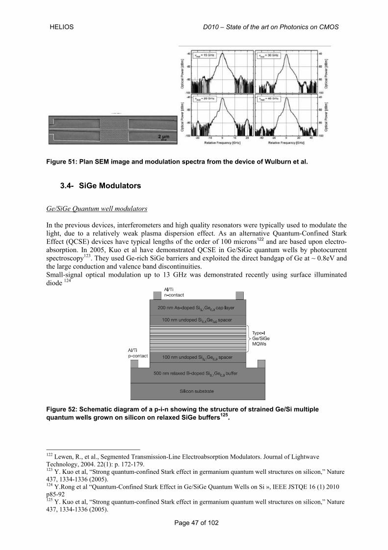
HELIOS D010 – State of the art on Photonics on CMOS
Page 47 of 102
Figure 51: Plan SEM image and modulation spectra from the device of Wulburn et al.
3.4- SiGe Modulators
Ge/SiGe Quantum well modulators In the previous devices, interferometers and high quality resonators were typically used to modulate the light, due to a relatively weak plasma dispersion effect. As an alternative Quantum-Confined Stark Effect (QCSE) devices have typical lengths of the order of 100 microns122 and are based upon electro-absorption. In 2005, Kuo et al have demonstrated QCSE in Ge/SiGe quantum wells by photocurrent spectroscopy123. They used Ge-rich SiGe barriers and exploited the direct bandgap of Ge at ~ 0.8eV and the large conduction and valence band discontinuities. Small-signal optical modulation up to 13 GHz was demonstrated recently using surface illuminated diode 124
Figure 52: Schematic diagram of a p-i-n showing the structure of strained Ge/Si multiple quantum wells grown on silicon on relaxed SiGe buffers125.
122 Lewen, R., et al., Segmented Transmission-Line Electroabsorption Modulators. Journal of Lightwave Technology, 2004. 22(1): p. 172-179. 123 Y. Kuo et al, “Strong quantum-confined Stark effect in germanium quantum well structures on silicon,” Nature 437, 1334-1336 (2005). 124 Y.Rong et al “Quantum-Confined Stark Effect in Ge/SiGe Quantum Wells on Si », IEEE JSTQE 16 (1) 2010 p85-92 125 Y. Kuo et al, “Strong quantum-confined Stark effect in germanium quantum well structures on silicon,” Nature 437, 1334-1336 (2005).
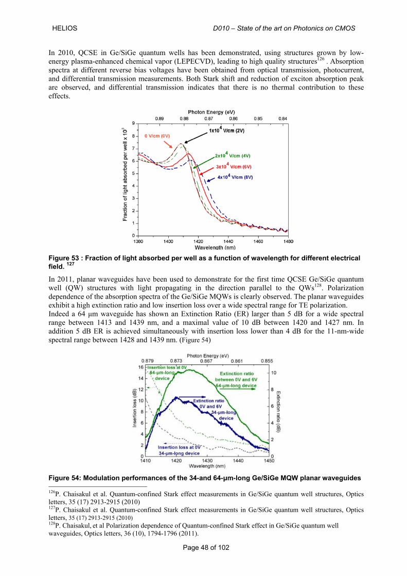
HELIOS D010 – State of the art on Photonics on CMOS
Page 48 of 102
In 2010, QCSE in Ge/SiGe quantum wells has been demonstrated, using structures grown by low-energy plasma-enhanced chemical vapor (LEPECVD), leading to high quality structures126 . Absorption spectra at different reverse bias voltages have been obtained from optical transmission, photocurrent, and differential transmission measurements. Both Stark shift and reduction of exciton absorption peak are observed, and differential transmission indicates that there is no thermal contribution to these effects.
Figure 53 : Fraction of light absorbed per well as a function of wavelength for different electrical field.
127
In 2011, planar waveguides have been used to demonstrate for the first time QCSE Ge/SiGe quantum well (QW) structures with light propagating in the direction parallel to the QWs128. Polarization dependence of the absorption spectra of the Ge/SiGe MQWs is clearly observed. The planar waveguides exhibit a high extinction ratio and low insertion loss over a wide spectral range for TE polarization. Indeed a 64 μm waveguide has shown an Extinction Ratio (ER) larger than 5 dB for a wide spectral range between 1413 and 1439 nm, and a maximal value of 10 dB between 1420 and 1427 nm. In addition 5 dB ER is achieved simultaneously with insertion loss lower than 4 dB for the 11-nm-wide spectral range between 1428 and 1439 nm. (Figure 54)
Figure 54: Modulation performances of the 34-and 64-μm-long Ge/SiGe MQW planar waveguides 126P. Chaisakul et al. Quantum-confined Stark effect measurements in Ge/SiGe quantum well structures, Optics letters, 35 (17) 2913-2915 (2010) 127P. Chaisakul et al. Quantum-confined Stark effect measurements in Ge/SiGe quantum well structures, Optics letters, 35 (17) 2913-2915 (2010) 128P. Chaisakul, et al Polarization dependence of Quantum-confined Stark effect in Ge/SiGe quantum well waveguides, Optics letters, 36 (10), 1794-1796 (2011).
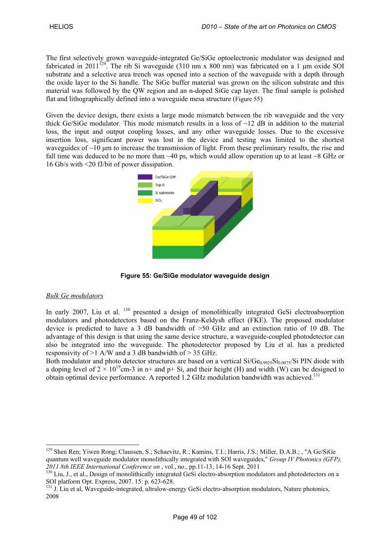
HELIOS D010 – State of the art on Photonics on CMOS
Page 49 of 102
The first selectively grown waveguide-integrated Ge/SiGe optoelectronic modulator was designed and fabricated in 2011129. The rib Si waveguide (310 nm x 800 nm) was fabricated on a 1 μm oxide SOI substrate and a selective area trench was opened into a section of the waveguide with a depth through the oxide layer to the Si handle. The SiGe buffer material was grown on the silicon substrate and this material was followed by the QW region and an n-doped SiGe cap layer. The final sample is polished flat and lithographically defined into a waveguide mesa structure (Figure 55) Given the device design, there exists a large mode mismatch between the rib waveguide and the very thick Ge/SiGe modulator. This mode mismatch results in a loss of ~12 dB in addition to the material loss, the input and output coupling losses, and any other waveguide losses. Due to the excessive insertion loss, significant power was lost in the device and testing was limited to the shortest waveguides of ~10 μm to increase the transmission of light. From these preliminary results, the rise and fall time was deduced to be no more than ~40 ps, which would allow operation up to at least ~8 GHz or 16 Gb/s with <20 fJ/bit of power dissipation.
Figure 55: Ge/SiGe modulator waveguide design
Bulk Ge modulators In early 2007, Liu et al. 130 presented a design of monolithically integrated GeSi electroabsorption modulators and photodetectors based on the Franz-Keldysh effect (FKE). The proposed modulator device is predicted to have a 3 dB bandwidth of >50 GHz and an extinction ratio of 10 dB. The advantage of this design is that using the same device structure, a waveguide-coupled photodetector can also be integrated into the waveguide. The photodetector proposed by Liu et al. has a predicted responsivity of >1 A/W and a 3 dB bandwidth of > 35 GHz. Both modulator and photo detector structures are based on a vertical Si/Ge0.9925Si0.0075/Si PIN diode with a doping level of 2 × 1019cm-3 in n+ and p+ Si, and their height (H) and width (W) can be designed to obtain optimal device performance. A reported 1.2 GHz modulation bandwidth was achieved.131
129 Shen Ren; Yiwen Rong; Claussen, S.; Schaevitz, R.; Kamins, T.I.; Harris, J.S.; Miller, D.A.B.; , "A Ge/SiGe quantum well waveguide modulator monolithically integrated with SOI waveguides," Group IV Photonics (GFP), 2011 8th IEEE International Conference on , vol., no., pp.11-13, 14-16 Sept. 2011 130 Liu, J., et al., Design of monolithically integrated GeSi electro-absorption modulators and photodetectors on a SOI platform Opt. Express, 2007. 15: p. 623-628. 131 J. Liu et al, Waveguide-integrated, ultralow-energy GeSi electro-absorption modulators, Nature photonics, 2008
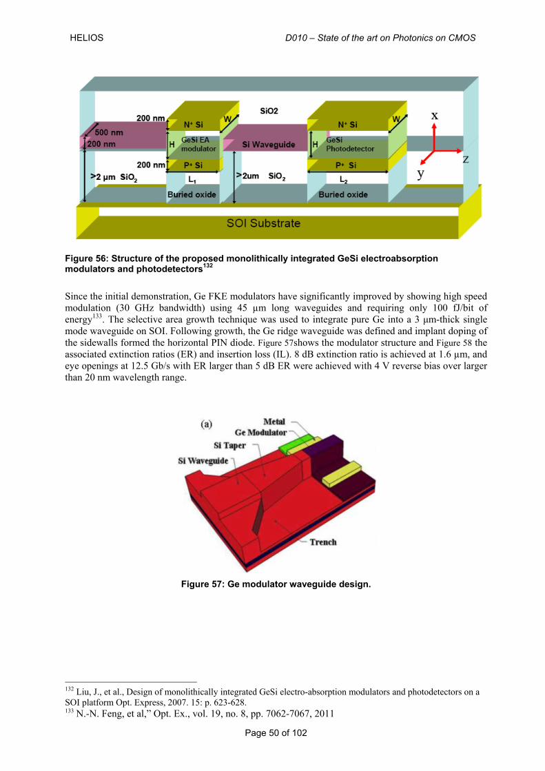
HELIOS D010 – State of the art on Photonics on CMOS
Page 50 of 102
Figure 56: Structure of the proposed monolithically integrated GeSi electroabsorption modulators and photodetectors132
Since the initial demonstration, Ge FKE modulators have significantly improved by showing high speed modulation (30 GHz bandwidth) using 45 µm long waveguides and requiring only 100 fJ/bit of energy133. The selective area growth technique was used to integrate pure Ge into a 3 μm-thick single mode waveguide on SOI. Following growth, the Ge ridge waveguide was defined and implant doping of the sidewalls formed the horizontal PIN diode. Figure 57shows the modulator structure and Figure 58 the associated extinction ratios (ER) and insertion loss (IL). 8 dB extinction ratio is achieved at 1.6 µm, and eye openings at 12.5 Gb/s with ER larger than 5 dB ER were achieved with 4 V reverse bias over larger than 20 nm wavelength range.
Figure 57: Ge modulator waveguide design.
132 Liu, J., et al., Design of monolithically integrated GeSi electro-absorption modulators and photodetectors on a SOI platform Opt. Express, 2007. 15: p. 623-628. 133 N.-N. Feng, et al,” Opt. Ex., vol. 19, no. 8, pp. 7062-7067, 2011
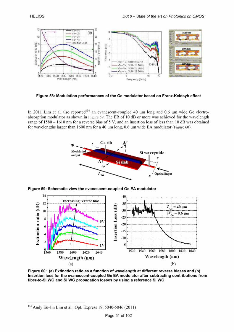
HELIOS D010 – State of the art on Photonics on CMOS
Page 51 of 102
Figure 58: Modulation performances of the Ge modulator based on Franz-Keldsyh effect In 2011 Lim et al also reported134 an evanescent-coupled 40 μm long and 0.6 μm wide Ge electro-absorption modulator as shown in Figure 59. The ER of 10 dB or more was achieved for the wavelength range of 1580 – 1610 nm for a reverse bias of 5 V, and an insertion loss of less than 10 dB was obtained for wavelengths larger than 1600 nm for a 40 μm long, 0.6 μm wide EA modulator (Figure 60).
Figure 59: Schematic view the evanescent-coupled Ge EA modulator
(a) (b)
Figure 60: (a) Extinction ratio as a function of wavelength at different reverse biases and (b) Insertion loss for the evanescent-coupled Ge EA modulator after subtracting contributions from fiber-to-Si WG and Si WG propagation losses by using a reference Si WG
134 Andy Eu-Jin Lim et al., Opt. Express 19, 5040-5046 (2011)
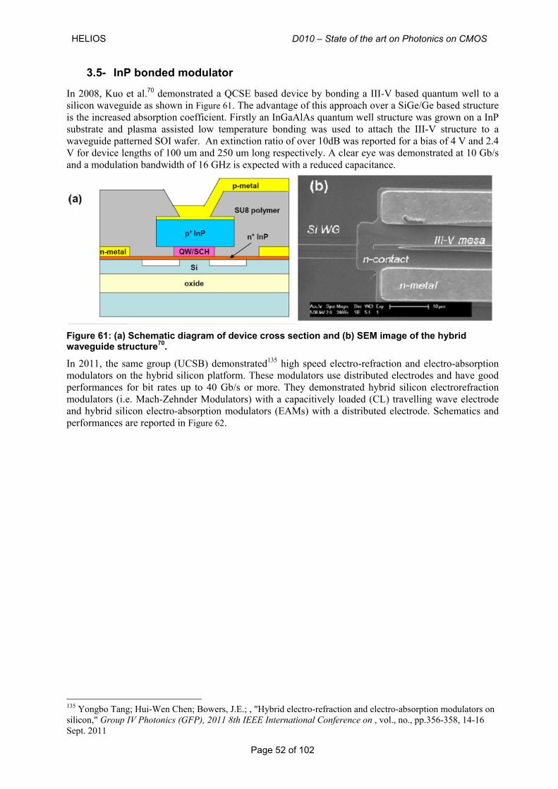
HELIOS D010 – State of the art on Photonics on CMOS
Page 52 of 102
3.5- InP bonded modulator
In 2008, Kuo et al.70 demonstrated a QCSE based device by bonding a III-V based quantum well to a silicon waveguide as shown in Figure 61. The advantage of this approach over a SiGe/Ge based structure is the increased absorption coefficient. Firstly an InGaAlAs quantum well structure was grown on a InP substrate and plasma assisted low temperature bonding was used to attach the III-V structure to a waveguide patterned SOI wafer. An extinction ratio of over 10dB was reported for a bias of 4 V and 2.4 V for device lengths of 100 um and 250 um long respectively. A clear eye was demonstrated at 10 Gb/s and a modulation bandwidth of 16 GHz is expected with a reduced capacitance.
Figure 61: (a) Schematic diagram of device cross section and (b) SEM image of the hybrid waveguide structure70.
In 2011, the same group (UCSB) demonstrated135 high speed electro-refraction and electro-absorption modulators on the hybrid silicon platform. These modulators use distributed electrodes and have good performances for bit rates up to 40 Gb/s or more. They demonstrated hybrid silicon electrorefraction modulators (i.e. Mach-Zehnder Modulators) with a capacitively loaded (CL) travelling wave electrode and hybrid silicon electro-absorption modulators (EAMs) with a distributed electrode. Schematics and performances are reported in Figure 62.
135 Yongbo Tang; Hui-Wen Chen; Bowers, J.E.; , "Hybrid electro-refraction and electro-absorption modulators on silicon," Group IV Photonics (GFP), 2011 8th IEEE International Conference on , vol., no., pp.356-358, 14-16 Sept. 2011
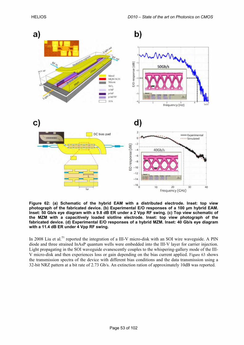
HELIOS D010 – State of the art on Photonics on CMOS
Page 53 of 102
Figure 62: (a) Schematic of the hybrid EAM with a distributed electrode. Inset: top view photograph of the fabricated device. (b) Experimental E/O responses of a 100 µm hybrid EAM. Inset: 50 Gb/s eye diagram with a 9.8 dB ER under a 2 Vpp RF swing. (c) Top view schematic of the MZM with a capacitively loaded slotline electrode. Inset: top view photograph of the fabricated device. (d) Experimental E/O responses of a hybrid MZM. Inset: 40 Gb/s eye diagram with a 11.4 dB ER under 4 Vpp RF swing.
In 2008 Liu et al.71 reported the integration of a III-V micro-disk with an SOI wire waveguide. A PIN diode and three strained InAsP quantum wells were embedded into the III-V layer for carrier injection. Light propagating in the SOI waveguide evanescently couples to the whispering-gallery mode of the III-V micro-disk and then experiences loss or gain depending on the bias current applied. Figure 63 shows the transmission spectra of the device with different bias conditions and the data transmission using a 32-bit NRZ pattern at a bit rate of 2.73 Gb/s. An extinction ration of approximately 10dB was reported.
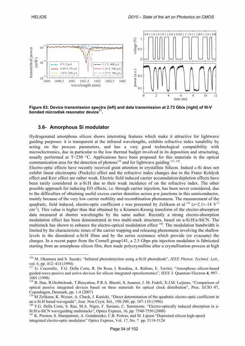
HELIOS D010 – State of the art on Photonics on CMOS
Page 54 of 102
Figure 63: Device transmission spectra (left) and data transmission at 2.73 Gb/s (right) of III-V bonded microdisk resonator device71.
3.6- Amorphous Si modulator
Hydrogenated amorphous silicon shows interesting features which make it attractive for lightwave guiding purposes: it is transparent at the infrared wavelengths, exhibits refractive index tunability by acting on the process parameters, and has a very good technological compatibility with microelectronics, due in particular to the low thermal budget involved in its deposition and structuring, usually performed at T<250 °C. Applications have been proposed for this materials in the optical communication area for the detection of photons136 and for lightwave guiding 137, 138 . Electro-optic effects have recently received great attention in crystalline Silicon. Indeed c-Si does not exhibit linear electrooptic (Pockels) effect and the refractive index changes due to the Franz–Keldysh effect and Kerr effect are rather weak. Electric field induced carrier accumulation/depletion effects have been rarely considered in a-Si:H due to their weak incidence of on the refractive index. The other possible approach for inducing EO effects, i.e. through carrier injection, has been never considered, due to the difficulties of obtaining useful excess carrier densities across p-n junctions in this semiconductor, mainly because of the very low carrier mobility and recombination phenomena. The measurement of the quadratic, field induced, electro-optic coefficient s was presented by Zelikson et al.139 (s=2.1×-14 V-2 cm-2). This value is higher than that obtained by a Kramers-Kronig transform of the electro-absorption data measured at shorter wavelengths by the same author. Recently a strong electro-absorption modulation effect has been demonstrated in two multi-stack structures, based on a-Si:H/a-SiCN. The multistack has shown to enhance the electro-optical modulation effect 140. The modulation bandwidth is limited by the characteristic times of the carrier trapping and releasing phenomena involving the shallow levels in the disordered a-Si:H films and by the series resistance which provide (or evacuate) the charges. In a recent paper from the Cornell group141, a 2.5 Gbps pin injection modulator is fabricated starting from an amorphous silicon film, then made polycrystalline after a crystallisation process at high
136 M. Okamura and S. Suzuki, “Infrared photodetection using a-Si:H photodiode”, IEEE Photon. Technol. Lett., vol. 6, pp. 412–414 (1994) 137 G. Cocorullo, F.G. Della Corte, R. De Rosa, I. Rendina, A. Rubino, E. Terzini, “Amorphous silicon-based guided-wave passive and active devices for silicon integrated optoelectronics”, IEEE J. Quantum Electron 4, 997–1001 (1998) 138 B. Han, R.Orobtchouk, T.Benyattou, P.R.A. Binetti, S. Jeannot, J. M. Fedeli, X.J.M. Leijtens, “Comparison of optical passive integrated devices based on three materials for optical clock distribution”, Proc. ECIO 07, Copenhagen, Denmark, pp. 1-4 (2007) 139 M Zelikson, K. Weiser, A. Chack, J. Kanicki, “Direct determination of the quadratic electro-optic coefficient in an a-Si:H based waveguide”, Jour. Non Cryst. Sol., 198-200, pp. 107-110 (1996) 140 F.G. Della Corte, S. Rao, M.A. Nigro, F. Suriano, C. Summonte, “Electro-optically induced absorption in a-Si:H/a-SiCN waveguiding multistacks”, Optics Express, 16, pp. 7540-7550 (2008) 141 K. Preston, S. Manipatruni, A. Gondarenko, C.B. Poitras, and M. Lipson “Deposited silicon high-speed integrated electro-optic modulator” Optics Express, Vol. 17, No. 7 pp. 5118-5124
HELIOS D010 – State of the art on Photonics on CMOS
Page 55 of 102
T. At the end, the paper also suggests using a conventional excimer lasers treatment for lower temperature crystallisation. . More recently, 100-fs-fast all-optical non linear effects have been reported142 in a-Si:H, and the optical Kerr effect coefficient has been estimated .
4- Photodiodes on Si
4.1- Photodiodes Ge on Si
Monolithically integrated Ge photodetectors on Si-based substrates is one of the favourite options for a photonics detection building block on a Si platform. Firstly, the top illuminated photodetector geometry was mainly studied in the last few years. Recently, waveguide integration of the Ge photodetector with SOI waveguides has encountered a high interest.
Waveguide integration presents several advantages, among them: • It promotes the integration of the photodetector with other silicon photonic components. • It allows an efficient light coupling between the waveguided input light and the detector. • High external quantum efficiency is also expected as the photodetector length can be a few
microns. • It permits having a large optical responsivity and a large bandwidth at the same time. In surface
illuminated photodetectors the depletion width has to be decreased by shrinking the undoped Ge thickness in order to obtain a high bandwidth value but at the expense of the absorption length and optical responsivity. On the other hand waveguide integrated pin and MSM Ge photodiodes show large values of the product of bandwidth time optical responsivity at 1550nm. Optical absorption of the guided mode and the carrier collection (in vertical or lateral directions) occur in perpendicular directions, which decouple their dependence. As the absorption length of Ge at 1.55um is few microns, it is possible to reduce the photodetector dimensions and at the same time its thickness.
Ge photodetectors structures are divided between Metal-Semiconductor-Metal (MSM) and PIN junctions. Two configurations of integration of the latter PIN Ge photodetectors with Si waveguides are possible: butt coupling and evanescent coupling. We first consider vertical pin junctions. The butt coupling is preferred in some cases, for example in the case of selective epitaxial growth in recesses etched in Si143. It has the advantage of a small absorption length. From simulations it was reported that no significant diffraction or reflection losses should be observed144. This configuration requires however technological constraints in precise Si etching and Ge selective growth. Vertical evanescent coupling is usually simpler from a technological point of view and was then largely studied but such coupling depends on the wavelength and the Ge thickness. It is shown in Figure 64 that large optical responsivities with comparable values are reported for both configurations. Most reported papers present a vertical PIN evanescent coupled photodetector and report responsivity values of 1A/W at 1.55μm and more than 40GHz bandwidth143, as shown in Figure 64 and Figure 65. The optical responsivity time bandwidth product is obviously much larger for waveguide integrated photodetectors than for surface illuminated photodetectors145. Recently, Wang et al154 published a comparison between vertical and lateral PIN photodetectors integrated in waveguide geometries. The dark current and the bandwidth values were roughly the same for both configurations and for equivalent diode size and mesa thickness, but optical responsivity was much larger in the lateral case (1.16A/W to be compared to 0.29A/W at 1.55μm and 5V reverse bias). 142 Y.Shoji et al., “Ultrafast nonlinear effects in hydrogenated amorphous silicon wire waveguide”, Optics Express, Vol. 18, No. 6, pp. 5668-5673 (2010) 143 Vivien et al. IEEE Group IV photonics 2008 conference proceedings (2008) 144 M. Rouvière, M. Halbwax, J.-C. Cercus, E. Cassan, L. Vivien, D. Pascal, et al. Optical Engineering 44, 075402 (2005) 145 M. Jutzi, M. Berroth, G. Wöhl, M. Oehme, E. Kasper. IEEE Photon. Technol. Lett. 17, 1510 (2005)
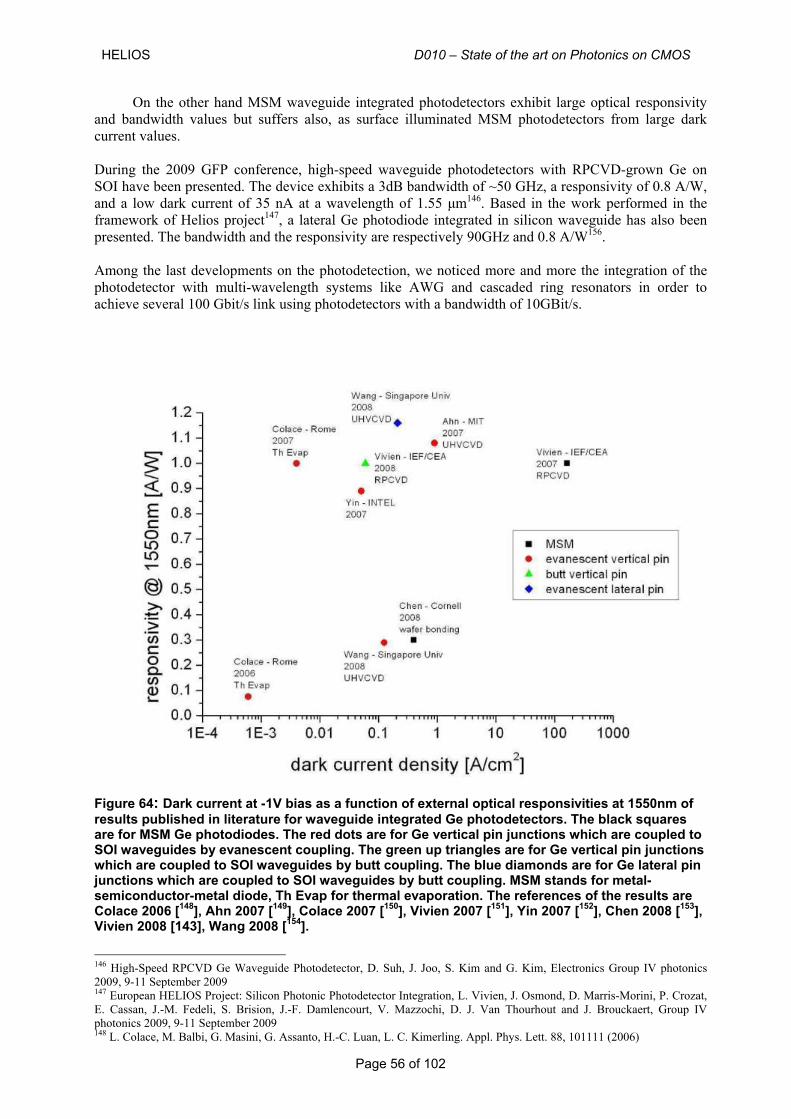
HELIOS D010 – State of the art on Photonics on CMOS
Page 56 of 102
On the other hand MSM waveguide integrated photodetectors exhibit large optical responsivity and bandwidth values but suffers also, as surface illuminated MSM photodetectors from large dark current values.
During the 2009 GFP conference, high-speed waveguide photodetectors with RPCVD-grown Ge on SOI have been presented. The device exhibits a 3dB bandwidth of ~50 GHz, a responsivity of 0.8 A/W, and a low dark current of 35 nA at a wavelength of 1.55 μm146. Based in the work performed in the framework of Helios project147, a lateral Ge photodiode integrated in silicon waveguide has also been presented. The bandwidth and the responsivity are respectively 90GHz and 0.8 A/W156. Among the last developments on the photodetection, we noticed more and more the integration of the photodetector with multi-wavelength systems like AWG and cascaded ring resonators in order to achieve several 100 Gbit/s link using photodetectors with a bandwidth of 10GBit/s.
Figure 64: Dark current at -1V bias as a function of external optical responsivities at 1550nm of results published in literature for waveguide integrated Ge photodetectors. The black squares are for MSM Ge photodiodes. The red dots are for Ge vertical pin junctions which are coupled to SOI waveguides by evanescent coupling. The green up triangles are for Ge vertical pin junctions which are coupled to SOI waveguides by butt coupling. The blue diamonds are for Ge lateral pin junctions which are coupled to SOI waveguides by butt coupling. MSM stands for metal-semiconductor-metal diode, Th Evap for thermal evaporation. The references of the results are Colace 2006 [148], Ahn 2007 [149], Colace 2007 [150], Vivien 2007 [151], Yin 2007 [152], Chen 2008 [153], Vivien 2008 [143], Wang 2008 [154].
146 High-Speed RPCVD Ge Waveguide Photodetector, D. Suh, J. Joo, S. Kim and G. Kim, Electronics Group IV photonics 2009, 9-11 September 2009 147 European HELIOS Project: Silicon Photonic Photodetector Integration, L. Vivien, J. Osmond, D. Marris-Morini, P. Crozat, E. Cassan, J.-M. Fedeli, S. Brision, J.-F. Damlencourt, V. Mazzochi, D. J. Van Thourhout and J. Brouckaert, Group IV photonics 2009, 9-11 September 2009 148 L. Colace, M. Balbi, G. Masini, G. Assanto, H.-C. Luan, L. C. Kimerling. Appl. Phys. Lett. 88, 101111 (2006)
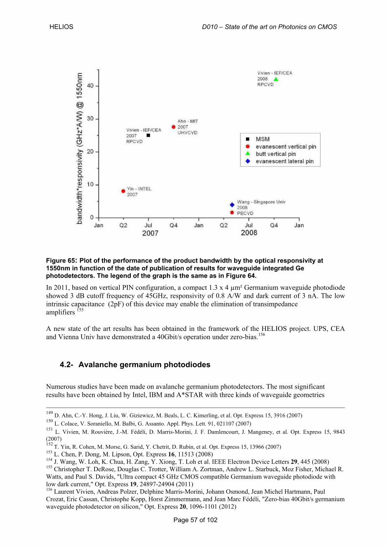
HELIOS D010 – State of the art on Photonics on CMOS
Page 57 of 102
Figure 65: Plot of the performance of the product bandwidth by the optical responsivity at 1550nm in function of the date of publication of results for waveguide integrated Ge photodetectors. The legend of the graph is the same as in Figure 64.
In 2011, based on vertical PIN configuration, a compact 1.3 x 4 µm² Germanium waveguide photodiode showed 3 dB cutoff frequency of 45GHz, responsivity of 0.8 A/W and dark current of 3 nA. The low intrinsic capacitance (2pF) of this device may enable the elimination of transimpedance amplifiers 155 A new state of the art results has been obtained in the framework of the HELIOS project. UPS, CEA and Vienna Univ have demonstrated a 40Gbit/s operation under zero-bias.156
4.2- Avalanche germanium photodiodes
Numerous studies have been made on avalanche germanium photodetectors. The most significant results have been obtained by Intel, IBM and A*STAR with three kinds of waveguide geometries
149 D. Ahn, C.-Y. Hong, J. Liu, W. Giziewicz, M. Beals, L. C. Kimerling, et al. Opt. Express 15, 3916 (2007) 150 L. Colace, V. Soraniello, M. Balbi, G. Assanto. Appl. Phys. Lett. 91, 021107 (2007) 151 L. Vivien, M. Rouvière, J.-M. Fédéli, D. Marris-Morini, J. F. Damlencourt, J. Mangeney, et al. Opt. Express 15, 9843 (2007) 152 T. Yin, R. Cohen, M. Morse, G. Sarid, Y. Chetrit, D. Rubin, et al. Opt. Express 15, 13966 (2007) 153 L. Chen, P. Dong, M. Lipson, Opt. Express 16, 11513 (2008) 154 J. Wang, W. Loh, K. Chua, H. Zang, Y. Xiong, T. Loh et al. IEEE Electron Device Letters 29, 445 (2008) 155 Christopher T. DeRose, Douglas C. Trotter, William A. Zortman, Andrew L. Starbuck, Moz Fisher, Michael R. Watts, and Paul S. Davids, "Ultra compact 45 GHz CMOS compatible Germanium waveguide photodiode with low dark current," Opt. Express 19, 24897-24904 (2011) 156 Laurent Vivien, Andreas Polzer, Delphine Marris-Morini, Johann Osmond, Jean Michel Hartmann, Paul Crozat, Eric Cassan, Christophe Kopp, Horst Zimmermann, and Jean Marc Fédéli, "Zero-bias 40Gbit/s germanium waveguide photodetector on silicon," Opt. Express 20, 1096-1101 (2012)
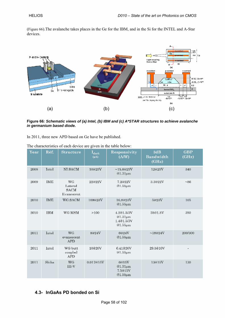
HELIOS D010 – State of the art on Photonics on CMOS
Page 58 of 102
(Figure 66).The avalanche takes places in the Ge for the IBM, and in the Si for the INTEL and A-Star devices.
(a) (b) (c)
Figure 66: Schematic views of (a) Intel, (b) IBM and (c) A*STAR structures to achieve avalanche in germanium based diode.
In 2011, three new APD based on Ge have be published. The characteristics of each device are given in the table below:
4.3- InGaAs PD bonded on Si
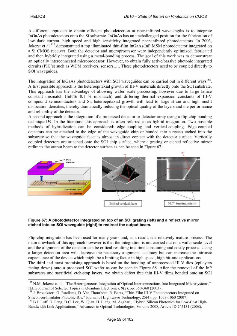
HELIOS D010 – State of the art on Photonics on CMOS
Page 59 of 102
A different approach to obtain efficient photodetection at near-infrared wavelengths is to integrate InGaAs photodetectors onto the Si substrate. InGaAs has an unchallenged position for the fabrication of low dark current, high speed and high sensitivity integrated near-infrared photodetectors. In 2003, Jokerst et al.157 demonstrated a top illuminated thin-film InGaAs/InP MSM photodetector integrated on a Si CMOS receiver. Both the detector and microprocessor were independently optimized, fabricated and then hybridly integrated using a metal-bonding process. The goal of this work was to demonstrate an optically interconnected microprocessor. However, to obtain fully active/passive photonic integrated circuits (PIC’s) such as WDM receivers, sensors,…. These photodetectors need to be coupled directly to SOI waveguides. The integration of InGaAs photodetectors with SOI waveguides can be carried out in different ways158. A first possible approach is the heteroepitaxial growth of III-V materials directly onto the SOI substrate. This approach has the advantage of allowing wafer scale processing, however due to large lattice constant mismatch (InP/Si 8.1 % mismatch) and differing thermal expansion constants of III-V compound semiconductors and Si, heteroepitaxial growth will lead to large strain and high misfit dislocation densities, thereby dramatically reducing the optical quality of the layers and the performance and reliability of the detector. A second approach is the integration of a processed detector or detector array using a flip-chip bonding technique159. In the literature, this approach is often referred to as hybrid integration. Two possible methods of hybridization can be considered: edge-coupling and vertical-coupling. Edge-coupled detectors can be attached to the edge of the waveguide chip or bonded into a recess etched into the substrate so that the waveguide facet is almost in direct contact with the detector surface. Vertically coupled detectors are attached onto the SOI chip surface, where a grating or etched reflective mirror redirects the output beam to the detector surface as can be seen in Figure 67. Figure 67: A photodetector integrated on top of an SOI grating (left) and a reflective mirror etched into an SOI waveguide (right) to redirect the output beam.
Flip-chip integration has been used for many years and, as a result, is a relatively mature process. The main drawback of this approach however is that the integration is not carried out on a wafer scale level and the alignment of the detector can be critical resulting in a time consuming and costly process. Using a larger detection area will decrease the necessary alignment accuracy but can increase the intrinsic capacitance of the device which might be a limiting factor in high speed, high bit-rate applications. The third and most promising approach is based on the bonding of unprocessed III-V dies (epilayers facing down) onto a processed SOI wafer as can be seen in Figure 68. After the removal of the InP substrates and sacrificial etch-stop layers, we obtain defect free thin III-V films bonded onto an SOI 157 N.M. Jokerst et al., “The Heterogeneous Integration of Optical Interconnections Into Integrated Microsystems,” IEEE Journal of Selected Topics in Quantum Electronics, 9(2), pp. 350-360 (2003). 158 J. Brouckaert, G. Roelkens, D. Van Thourhout, R. Baets, “Thin-Film III-V Photodetectors Integrated on Silicon-on-Insulator Photonic ICs,” Journal of Lightwave Technology, 25(4), pp. 1053-1060 (2007). 159 B.J. Luff, D. Feng, D.C. Lee, W. Qian, H. Liang, M. Asghari, “Hybrid Silicon Photonics for Low-Cost High-Bandwidth Link Applications,” Advances in Optical Technologies, Volume 2008, Article ID 245131 (2008).
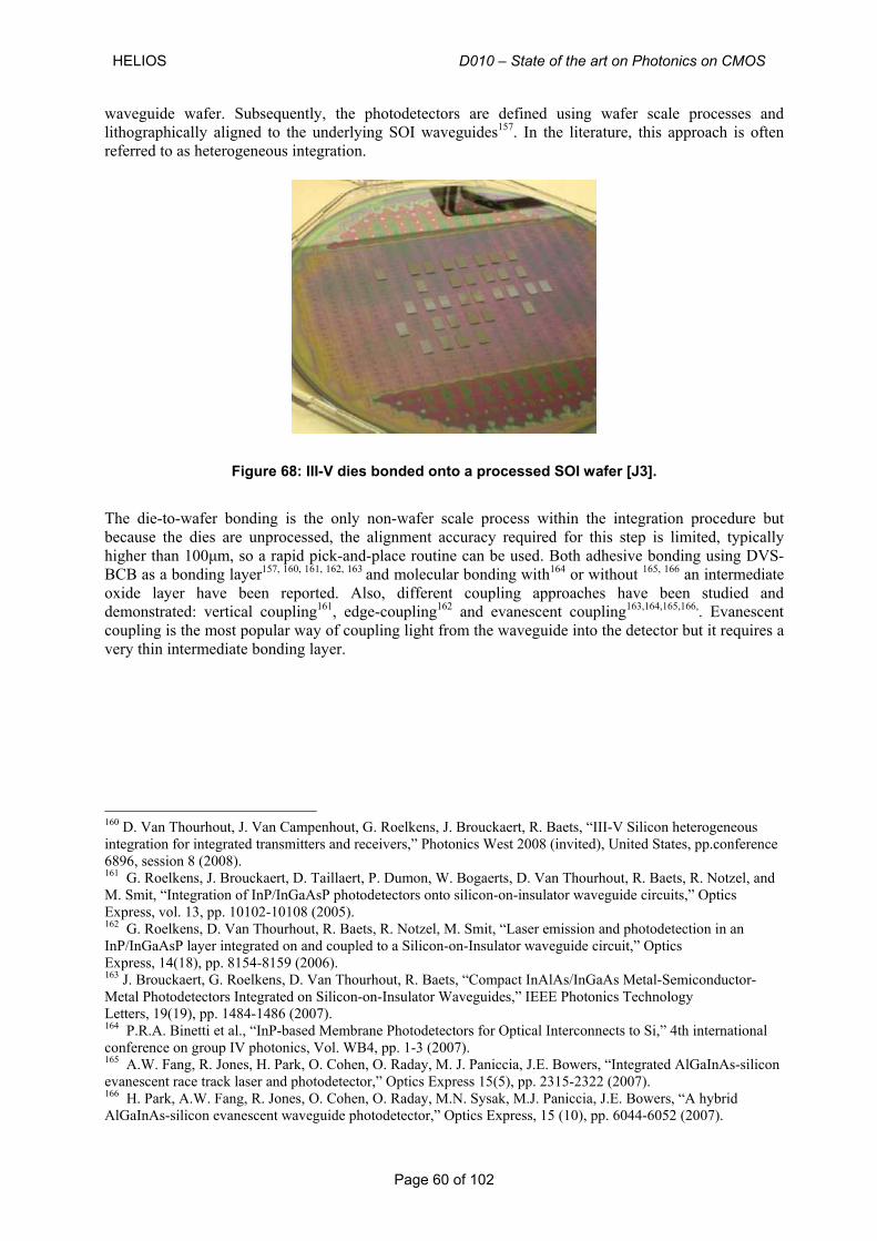
HELIOS D010 – State of the art on Photonics on CMOS
Page 60 of 102
waveguide wafer. Subsequently, the photodetectors are defined using wafer scale processes and lithographically aligned to the underlying SOI waveguides157. In the literature, this approach is often referred to as heterogeneous integration.
Figure 68: III-V dies bonded onto a processed SOI wafer [J3].
The die-to-wafer bonding is the only non-wafer scale process within the integration procedure but because the dies are unprocessed, the alignment accuracy required for this step is limited, typically higher than 100μm, so a rapid pick-and-place routine can be used. Both adhesive bonding using DVS-BCB as a bonding layer157, 160, 161, 162, 163 and molecular bonding with164 or without 165, 166 an intermediate oxide layer have been reported. Also, different coupling approaches have been studied and demonstrated: vertical coupling161, edge-coupling162 and evanescent coupling163,164,165,166,. Evanescent coupling is the most popular way of coupling light from the waveguide into the detector but it requires a very thin intermediate bonding layer.
160 D. Van Thourhout, J. Van Campenhout, G. Roelkens, J. Brouckaert, R. Baets, “III-V Silicon heterogeneous integration for integrated transmitters and receivers,” Photonics West 2008 (invited), United States, pp.conference 6896, session 8 (2008). 161 G. Roelkens, J. Brouckaert, D. Taillaert, P. Dumon, W. Bogaerts, D. Van Thourhout, R. Baets, R. Notzel, and M. Smit, “Integration of InP/InGaAsP photodetectors onto silicon-on-insulator waveguide circuits,” Optics Express, vol. 13, pp. 10102-10108 (2005). 162 G. Roelkens, D. Van Thourhout, R. Baets, R. Notzel, M. Smit, “Laser emission and photodetection in an InP/InGaAsP layer integrated on and coupled to a Silicon-on-Insulator waveguide circuit,” Optics Express, 14(18), pp. 8154-8159 (2006). 163 J. Brouckaert, G. Roelkens, D. Van Thourhout, R. Baets, “Compact InAlAs/InGaAs Metal-Semiconductor-Metal Photodetectors Integrated on Silicon-on-Insulator Waveguides,” IEEE Photonics Technology Letters, 19(19), pp. 1484-1486 (2007). 164 P.R.A. Binetti et al., “InP-based Membrane Photodetectors for Optical Interconnects to Si,” 4th international conference on group IV photonics, Vol. WB4, pp. 1-3 (2007). 165 A.W. Fang, R. Jones, H. Park, O. Cohen, O. Raday, M. J. Paniccia, J.E. Bowers, “Integrated AlGaInAs-silicon evanescent race track laser and photodetector,” Optics Express 15(5), pp. 2315-2322 (2007). 166 H. Park, A.W. Fang, R. Jones, O. Cohen, O. Raday, M.N. Sysak, M.J. Paniccia, J.E. Bowers, “A hybrid AlGaInAs-silicon evanescent waveguide photodetector,” Optics Express, 15 (10), pp. 6044-6052 (2007).
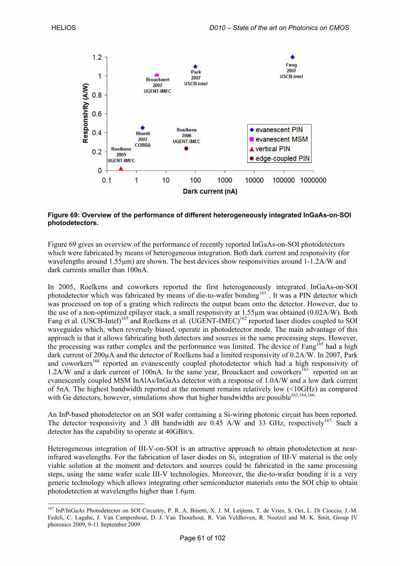
HELIOS D010 – State of the art on Photonics on CMOS
Page 61 of 102
Figure 69: Overview of the performance of different heterogeneously integrated InGaAs-on-SOI photodetectors.
Figure 69 gives an overview of the performance of recently reported InGaAs-on-SOI photodetectors which were fabricated by means of heterogeneous integration. Both dark current and responsivity (for wavelengths around 1.55µm) are shown. The best devices show responsivities around 1-1.2A/W and dark currents smaller than 100nA. In 2005, Roelkens and coworkers reported the first heterogeneously integrated InGaAs-on-SOI photodetector which was fabricated by means of die-to-wafer bonding161 . It was a PIN detector which was processed on top of a grating which redirects the output beam onto the detector. However, due to the use of a non-optimized epilayer stack, a small responsivity at 1.55µm was obtained (0.02A/W). Both Fang et al. (USCB-Intel)165 and Roelkens et al. (UGENT-IMEC)162 reported laser diodes coupled to SOI waveguides which, when reversely biased, operate in photodetector mode. The main advantage of this approach is that it allows fabricating both detectors and sources in the same processing steps. However, the processing was rather complex and the performance was limited. The device of Fang165 had a high dark current of 200µA and the detector of Roelkens had a limited responsivity of 0.2A/W. In 2007, Park and coworkers166 reported an evanescently coupled photodetector which had a high responsivity of 1.2A/W and a dark current of 100nA. In the same year, Brouckaert and coworkers163 reported on an evanescently coupled MSM InAlAs/InGaAs detector with a response of 1.0A/W and a low dark current of 5nA. The highest bandwidth reported at the moment remains relatively low (<10GHz) as compared with Ge detectors, however, simulations show that higher bandwidths are possible163,164,166. An InP-based photodetector on an SOI wafer containing a Si-wiring photonic circuit has been reported. The detector responsivity and 3 dB bandwidth are 0.45 A/W and 33 GHz, respectively167. Such a detector has the capability to operate at 40GBit/s. Heterogeneous integration of III-V-on-SOI is an attractive approach to obtain photodetection at near-infrared wavelengths. For the fabrication of laser diodes on Si, integration of III-V material is the only viable solution at the moment and detectors and sources could be fabricated in the same processing steps, using the same wafer scale III-V technologies. Moreover, the die-to-wafer bonding it is a very generic technology which allows integrating other semiconductor materials onto the SOI chip to obtain photodetection at wavelengths higher than 1.6µm. 167 InP/InGaAs Photodetector on SOI Circuitry, P. R. A. Binetti, X. J. M. Leijtens, T. de Vries, S. Oei, L. Di Cioccio, J.-M. Fedeli, C. Lagahe, J. Van Campenhout, D. J. Van Thourhout, R. Van Veldhoven, R. Noetzel and M. K. Smit, Group IV photonics 2009, 9-11 September 2009
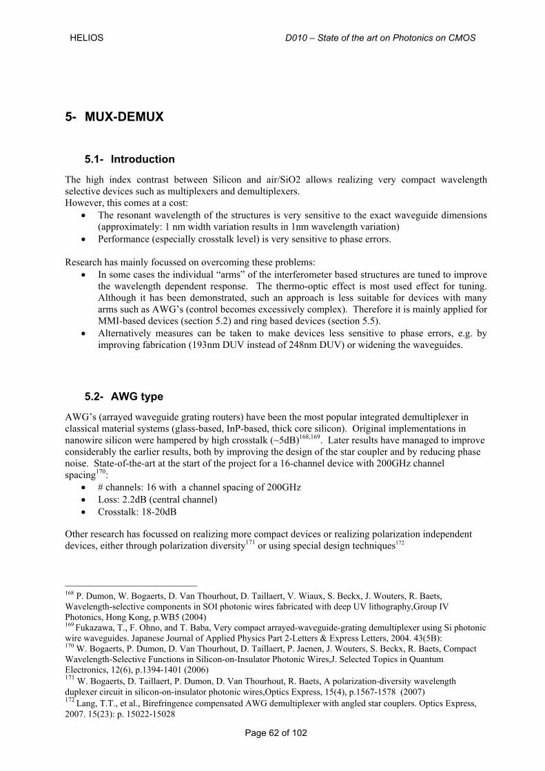
HELIOS D010 – State of the art on Photonics on CMOS
Page 62 of 102
5- MUX-DEMUX
5.1- Introduction
The high index contrast between Silicon and air/SiO2 allows realizing very compact wavelength selective devices such as multiplexers and demultiplexers. However, this comes at a cost:
• The resonant wavelength of the structures is very sensitive to the exact waveguide dimensions (approximately: 1 nm width variation results in 1nm wavelength variation)
• Performance (especially crosstalk level) is very sensitive to phase errors.
Research has mainly focussed on overcoming these problems: • In some cases the individual “arms” of the interferometer based structures are tuned to improve
the wavelength dependent response. The thermo-optic effect is most used effect for tuning. Although it has been demonstrated, such an approach is less suitable for devices with many arms such as AWG’s (control becomes excessively complex). Therefore it is mainly applied for MMI-based devices (section 5.2) and ring based devices (section 5.5).
• Alternatively measures can be taken to make devices less sensitive to phase errors, e.g. by improving fabrication (193nm DUV instead of 248nm DUV) or widening the waveguides.
5.2- AWG type
AWG’s (arrayed waveguide grating routers) have been the most popular integrated demultiplexer in classical material systems (glass-based, InP-based, thick core silicon). Original implementations in nanowire silicon were hampered by high crosstalk (~5dB)168,169. Later results have managed to improve considerably the earlier results, both by improving the design of the star coupler and by reducing phase noise. State-of-the-art at the start of the project for a 16-channel device with 200GHz channel spacing170:
• # channels: 16 with a channel spacing of 200GHz • Loss: 2.2dB (central channel) • Crosstalk: 18-20dB
Other research has focussed on realizing more compact devices or realizing polarization independent devices, either through polarization diversity171 or using special design techniques172
168 P. Dumon, W. Bogaerts, D. Van Thourhout, D. Taillaert, V. Wiaux, S. Beckx, J. Wouters, R. Baets, Wavelength-selective components in SOI photonic wires fabricated with deep UV lithography,Group IV Photonics, Hong Kong, p.WB5 (2004) 169 Fukazawa, T., F. Ohno, and T. Baba, Very compact arrayed-waveguide-grating demultiplexer using Si photonic wire waveguides. Japanese Journal of Applied Physics Part 2-Letters & Express Letters, 2004. 43(5B): 170 W. Bogaerts, P. Dumon, D. Van Thourhout, D. Taillaert, P. Jaenen, J. Wouters, S. Beckx, R. Baets, Compact Wavelength-Selective Functions in Silicon-on-Insulator Photonic Wires,J. Selected Topics in Quantum Electronics, 12(6), p.1394-1401 (2006) 171 W. Bogaerts, D. Taillaert, P. Dumon, D. Van Thourhout, R. Baets, A polarization-diversity wavelength duplexer circuit in silicon-on-insulator photonic wires,Optics Express, 15(4), p.1567-1578 (2007) 172 Lang, T.T., et al., Birefringence compensated AWG demultiplexer with angled star couplers. Optics Express, 2007. 15(23): p. 15022-15028
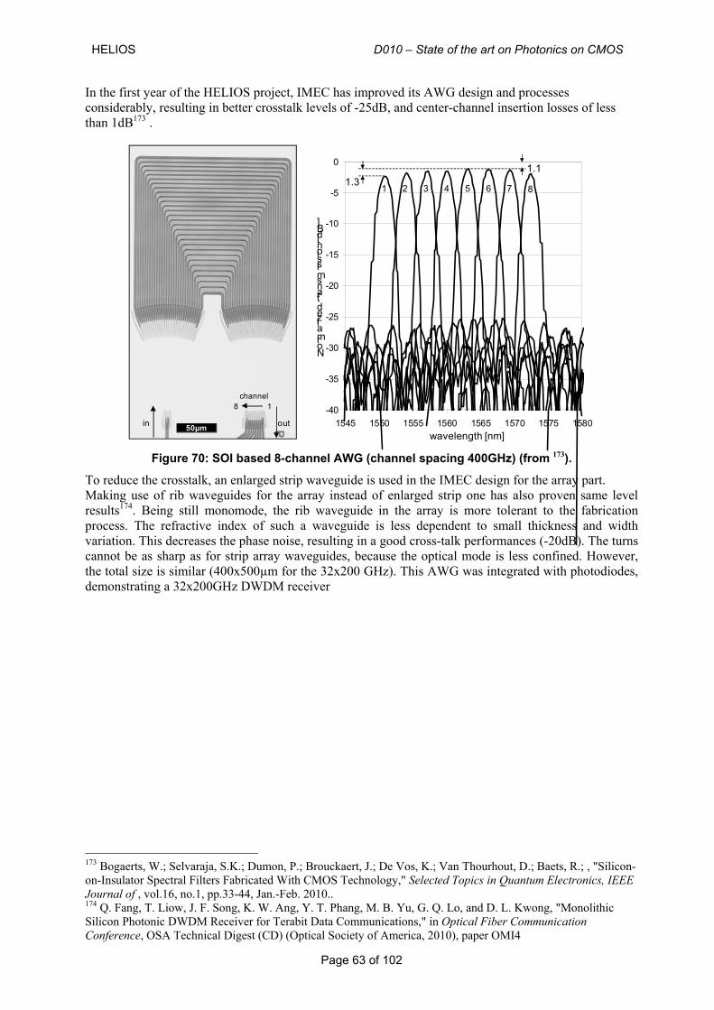
HELIOS D010 – State of the art on Photonics on CMOS
Page 63 of 102
In the first year of the HELIOS project, IMEC has improved its AWG design and processes considerably, resulting in better crosstalk levels of -25dB, and center-channel insertion losses of less than 1dB173 .
50µm
channel18
in out
-40
-35
-30
-25
-20
-15
-10
-5
0
1545 1550 1555 1560 1565 1570 1575 1580wavelength [nm]
Normalized transmission [dB]
1 2 3 4 5 6 7 81.3
1.1
Figure 70: SOI based 8-channel AWG (channel spacing 400GHz) (from 173).
To reduce the crosstalk, an enlarged strip waveguide is used in the IMEC design for the array part. Making use of rib waveguides for the array instead of enlarged strip one has also proven same level results174. Being still monomode, the rib waveguide in the array is more tolerant to the fabrication process. The refractive index of such a waveguide is less dependent to small thickness and width variation. This decreases the phase noise, resulting in a good cross-talk performances (-20dB). The turns cannot be as sharp as for strip array waveguides, because the optical mode is less confined. However, the total size is similar (400x500µm for the 32x200 GHz). This AWG was integrated with photodiodes, demonstrating a 32x200GHz DWDM receiver
173 Bogaerts, W.; Selvaraja, S.K.; Dumon, P.; Brouckaert, J.; De Vos, K.; Van Thourhout, D.; Baets, R.; , "Silicon-on-Insulator Spectral Filters Fabricated With CMOS Technology," Selected Topics in Quantum Electronics, IEEE Journal of , vol.16, no.1, pp.33-44, Jan.-Feb. 2010.. 174 Q. Fang, T. Liow, J. F. Song, K. W. Ang, Y. T. Phang, M. B. Yu, G. Q. Lo, and D. L. Kwong, "Monolithic Silicon Photonic DWDM Receiver for Terabit Data Communications," in Optical Fiber Communication Conference, OSA Technical Digest (CD) (Optical Society of America, 2010), paper OMI4
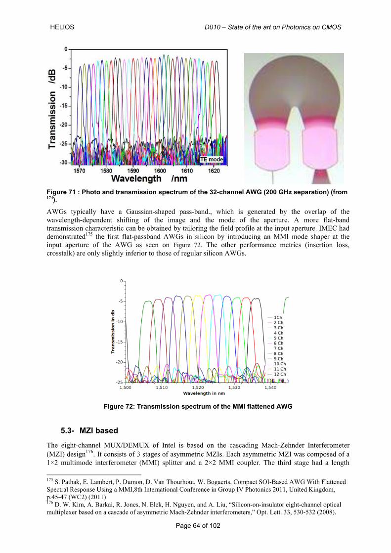
HELIOS D010 – State of the art on Photonics on CMOS
Page 64 of 102
Figure 71 : Photo and transmission spectrum of the 32-channel AWG (200 GHz separation) (from
174).
AWGs typically have a Gaussian-shaped pass-band., which is generated by the overlap of the wavelength-dependent shifting of the image and the mode of the aperture. A more flat-band transmission characteristic can be obtained by tailoring the field profile at the input aperture. IMEC had demonstrated175 the first flat-passband AWGs in silicon by introducing an MMI mode shaper at the input aperture of the AWG as seen on Figure 72. The other performance metrics (insertion loss, crosstalk) are only slightly inferior to those of regular silicon AWGs.
Figure 72: Transmission spectrum of the MMI flattened AWG
5.3- MZI based
The eight-channel MUX/DEMUX of Intel is based on the cascading Mach-Zehnder Interferometer (MZI) design176. It consists of 3 stages of asymmetric MZIs. Each asymmetric MZI was composed of a 1×2 multimode interferometer (MMI) splitter and a 2×2 MMI coupler. The third stage had a length 175 S. Pathak, E. Lambert, P. Dumon, D. Van Thourhout, W. Bogaerts, Compact SOI-Based AWG With Flattened Spectral Response Using a MMI,8th International Conference in Group IV Photonics 2011, United Kingdom, p.45-47 (WC2) (2011) 176 D. W. Kim, A. Barkai, R. Jones, N. Elek, H. Nguyen, and A. Liu, “Silicon-on-insulator eight-channel optical multiplexer based on a cascade of asymmetric Mach-Zehnder interferometers,” Opt. Lett. 33, 530-532 (2008).
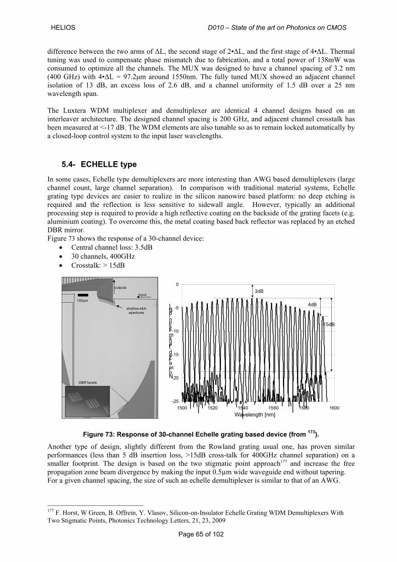
HELIOS D010 – State of the art on Photonics on CMOS
Page 65 of 102
difference between the two arms of ΔL, the second stage of 2•ΔL, and the first stage of 4•ΔL. Thermal tuning was used to compensate phase mismatch due to fabrication, and a total power of 138mW was consumed to optimize all the channels. The MUX was designed to have a channel spacing of 3.2 nm (400 GHz) with 4•ΔL = 97.2μm around 1550nm. The fully tuned MUX showed an adjacent channel isolation of 13 dB, an excess loss of 2.6 dB, and a channel uniformity of 1.5 dB over a 25 nm wavelength span. The Luxtera WDM multiplexer and demultiplexer are identical 4 channel designs based on an interleaver architecture. The designed channel spacing is 200 GHz, and adjacent channel crosstalk has been measured at <-17 dB. The WDM elements are also tunable so as to remain locked automatically by a closed-loop control system to the input laser wavelengths.
5.4- ECHELLE type
In some cases, Echelle type demultiplexers are more interesting than AWG based demultiplexers (large channel count, large channel separation). In comparison with traditional material systems, Echelle grating type devices are easier to realize in the silicon nanowire based platform: no deep etching is required and the reflection is less sensitive to sidewall angle. However, typically an additional processing step is required to provide a high reflective coating on the backside of the grating facets (e.g. aluminium coating). To overcome this, the metal coating based back reflector was replaced by an etched DBR mirror. Figure 73 shows the response of a 30-channel device:
• Central channel loss: 3.5dB • 30 channels, 400GHz • Crosstalk: > 15dB
shallow etchapertures
DBR facets
input
outputs
100µm
-25
-20
-15
-10
-5
0
1500 1520 1540 1560 1580 1600Wavelength [nm]
Normalized transmission [dB]
3dB
4dB
15dB
Figure 73: Response of 30-channel Echelle grating based device (from 173).
Another type of design, slightly different from the Rowland grating usual one, has proven similar performances (less than 5 dB insertion loss, >15dB cross-talk for 400GHz channel separation) on a smaller footprint. The design is based on the two stigmatic point approach177 and increase the free propagation zone beam divergence by making the input 0.5µm wide waveguide end without tapering. For a given channel spacing, the size of such an echelle demultiplexer is similar to that of an AWG.
177 F. Horst, W Green, B. Offrein, Y. Vlasov, Silicon-on-Insulator Echelle Grating WDM Demultiplexers With Two Stigmatic Points, Photonics Technology Letters, 21, 23, 2009
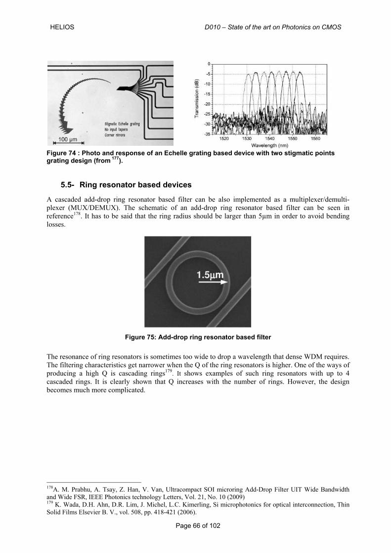
HELIOS D010 – State of the art on Photonics on CMOS
Page 66 of 102
Figure 74 : Photo and response of an Echelle grating based device with two stigmatic points grating design (from 177).
5.5- Ring resonator based devices
A cascaded add-drop ring resonator based filter can be also implemented as a multiplexer/demulti-plexer (MUX/DEMUX). The schematic of an add-drop ring resonator based filter can be seen in reference178. It has to be said that the ring radius should be larger than 5µm in order to avoid bending losses.
Figure 75: Add-drop ring resonator based filter
The resonance of ring resonators is sometimes too wide to drop a wavelength that dense WDM requires. The filtering characteristics get narrower when the Q of the ring resonators is higher. One of the ways of producing a high Q is cascading rings179. It shows examples of such ring resonators with up to 4 cascaded rings. It is clearly shown that Q increases with the number of rings. However, the design becomes much more complicated.
178A. M. Prabhu, A. Tsay, Z. Han, V. Van, Ultracompact SOI microring Add-Drop Filter UIT Wide Bandwidth and Wide FSR, IEEE Photonics technology Letters, Vol. 21, No. 10 (2009) 179 K. Wada, D.H. Ahn, D.R. Lim, J. Michel, L.C. Kimerling, Si microphotonics for optical interconnection, Thin Solid Films Elsevier B. V., vol. 508, pp. 418-421 (2006).
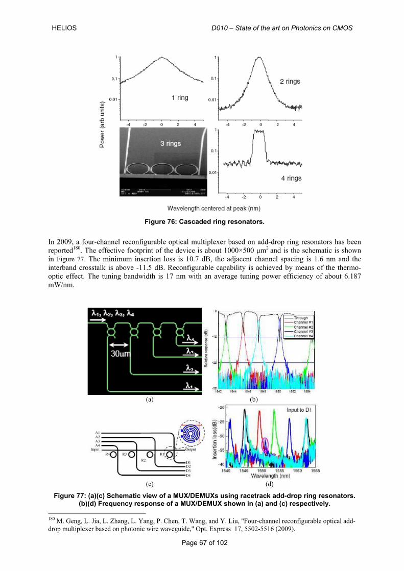
HELIOS D010 – State of the art on Photonics on CMOS
Page 67 of 102
Figure 76: Cascaded ring resonators.
In 2009, a four-channel reconfigurable optical multiplexer based on add-drop ring resonators has been reported180. The effective footprint of the device is about 1000×500 μm2 and is the schematic is shown in Figure 77. The minimum insertion loss is 10.7 dB, the adjacent channel spacing is 1.6 nm and the interband crosstalk is above -11.5 dB. Reconfigurable capability is achieved by means of the thermo-optic effect. The tuning bandwidth is 17 nm with an average tuning power efficiency of about 6.187 mW/nm.
(a) (b)
(c) (d)
Figure 77: (a)(c) Schematic view of a MUX/DEMUXs using racetrack add-drop ring resonators. (b)(d) Frequency response of a MUX/DEMUX shown in (a) and (c) respectively.
180 M. Geng, L. Jia, L. Zhang, L. Yang, P. Chen, T. Wang, and Y. Liu, "Four-channel reconfigurable optical add-drop multiplexer based on photonic wire waveguide," Opt. Express 17, 5502-5516 (2009).
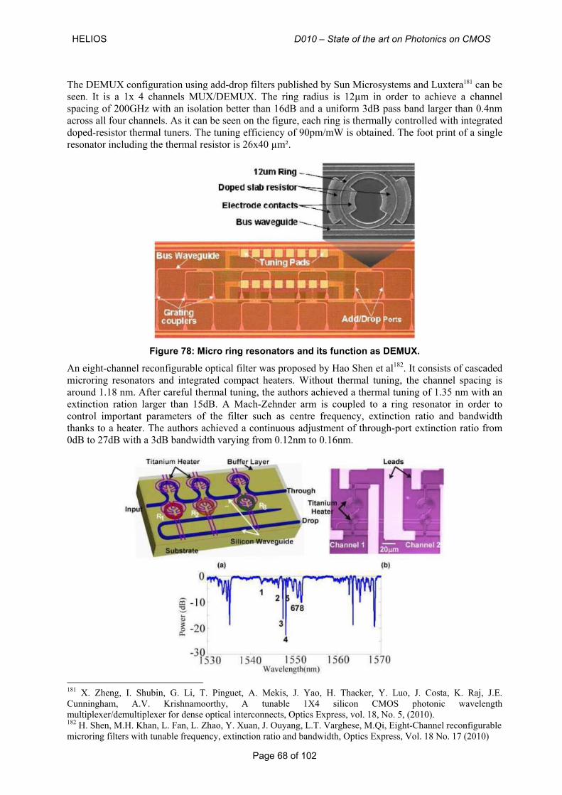
HELIOS D010 – State of the art on Photonics on CMOS
Page 68 of 102
The DEMUX configuration using add-drop filters published by Sun Microsystems and Luxtera181 can be seen. It is a 1x 4 channels MUX/DEMUX. The ring radius is 12µm in order to achieve a channel spacing of 200GHz with an isolation better than 16dB and a uniform 3dB pass band larger than 0.4nm across all four channels. As it can be seen on the figure, each ring is thermally controlled with integrated doped-resistor thermal tuners. The tuning efficiency of 90pm/mW is obtained. The foot print of a single resonator including the thermal resistor is 26x40 µm².
Figure 78: Micro ring resonators and its function as DEMUX.
An eight-channel reconfigurable optical filter was proposed by Hao Shen et al182. It consists of cascaded microring resonators and integrated compact heaters. Without thermal tuning, the channel spacing is around 1.18 nm. After careful thermal tuning, the authors achieved a thermal tuning of 1.35 nm with an extinction ration larger than 15dB. A Mach-Zehnder arm is coupled to a ring resonator in order to control important parameters of the filter such as centre frequency, extinction ratio and bandwidth thanks to a heater. The authors achieved a continuous adjustment of through-port extinction ratio from 0dB to 27dB with a 3dB bandwidth varying from 0.12nm to 0.16nm.
181 X. Zheng, I. Shubin, G. Li, T. Pinguet, A. Mekis, J. Yao, H. Thacker, Y. Luo, J. Costa, K. Raj, J.E. Cunningham, A.V. Krishnamoorthy, A tunable 1X4 silicon CMOS photonic wavelength multiplexer/demultiplexer for dense optical interconnects, Optics Express, vol. 18, No. 5, (2010). 182 H. Shen, M.H. Khan, L. Fan, L. Zhao, Y. Xuan, J. Ouyang, L.T. Varghese, M.Qi, Eight-Channel reconfigurable microring filters with tunable frequency, extinction ratio and bandwidth, Optics Express, Vol. 18 No. 17 (2010)
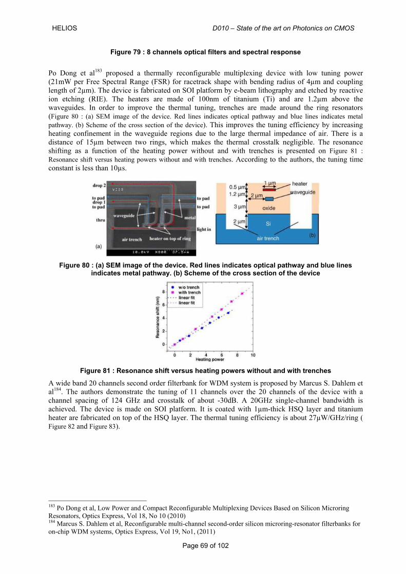
HELIOS D010 – State of the art on Photonics on CMOS
Page 69 of 102
Figure 79 : 8 channels optical filters and spectral response
Po Dong et al183 proposed a thermally reconfigurable multiplexing device with low tuning power (21mW per Free Spectral Range (FSR) for racetrack shape with bending radius of 4µm and coupling length of 2µm). The device is fabricated on SOI platform by e-beam lithography and etched by reactive ion etching (RIE). The heaters are made of 100nm of titanium (Ti) and are 1.2µm above the waveguides. In order to improve the thermal tuning, trenches are made around the ring resonators (Figure 80 : (a) SEM image of the device. Red lines indicates optical pathway and blue lines indicates metal pathway. (b) Scheme of the cross section of the device). This improves the tuning efficiency by increasing heating confinement in the waveguide regions due to the large thermal impedance of air. There is a distance of 15µm between two rings, which makes the thermal crosstalk negligible. The resonance shifting as a function of the heating power without and with trenches is presented on Figure 81 : Resonance shift versus heating powers without and with trenches. According to the authors, the tuning time constant is less than 10µs.
Figure 80 : (a) SEM image of the device. Red lines indicates optical pathway and blue lines
indicates metal pathway. (b) Scheme of the cross section of the device
Figure 81 : Resonance shift versus heating powers without and with trenches
A wide band 20 channels second order filterbank for WDM system is proposed by Marcus S. Dahlem et al184. The authors demonstrate the tuning of 11 channels over the 20 channels of the device with a channel spacing of 124 GHz and crosstalk of about -30dB. A 20GHz single-channel bandwidth is achieved. The device is made on SOI platform. It is coated with 1µm-thick HSQ layer and titanium heater are fabricated on top of the HSQ layer. The thermal tuning efficiency is about 27µW/GHz/ring ( Figure 82 and Figure 83).
183 Po Dong et al, Low Power and Compact Reconfigurable Multiplexing Devices Based on Silicon Microring Resonators, Optics Express, Vol 18, No 10 (2010) 184 Marcus S. Dahlem et al, Reconfigurable multi-channel second-order silicon microring-resonator filterbanks for on-chip WDM systems, Optics Express, Vol 19, No1, (2011)
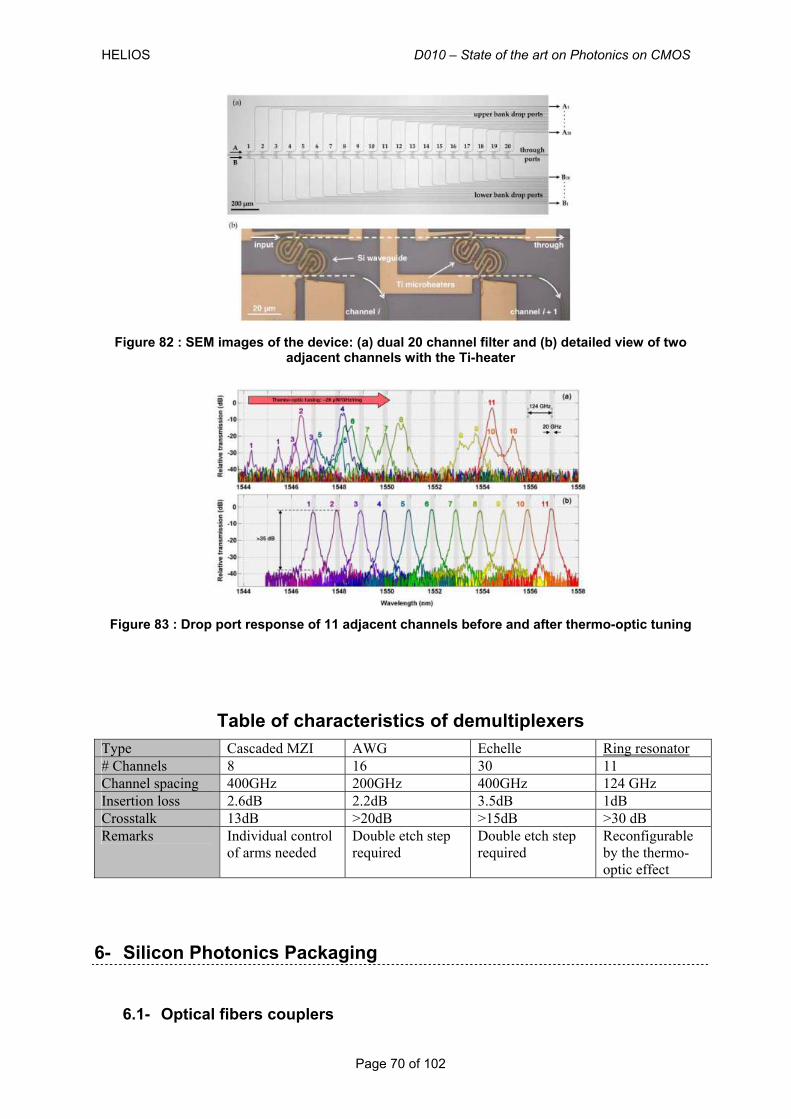
HELIOS D010 – State of the art on Photonics on CMOS
Page 70 of 102
Figure 82 : SEM images of the device: (a) dual 20 channel filter and (b) detailed view of two
adjacent channels with the Ti-heater
Figure 83 : Drop port response of 11 adjacent channels before and after thermo-optic tuning
Table of characteristics of demultiplexers Type Cascaded MZI AWG Echelle Ring resonator
# Channels 8 16 30 11 Channel spacing 400GHz 200GHz 400GHz 124 GHz Insertion loss 2.6dB 2.2dB 3.5dB 1dB Crosstalk 13dB >20dB >15dB >30 dB Remarks Individual control
of arms needed Double etch step required
Double etch step required
Reconfigurable by the thermo-optic effect
6- Silicon Photonics Packaging
6.1- Optical fibers couplers
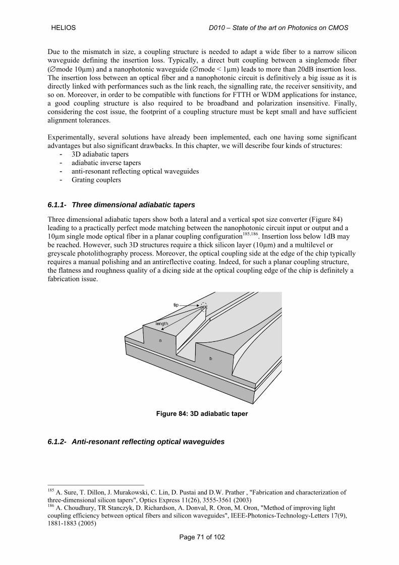
HELIOS D010 – State of the art on Photonics on CMOS
Page 71 of 102
Due to the mismatch in size, a coupling structure is needed to adapt a wide fiber to a narrow silicon waveguide defining the insertion loss. Typically, a direct butt coupling between a singlemode fiber (∅mode 10µm) and a nanophotonic waveguide (∅mode < 1µm) leads to more than 20dB insertion loss. The insertion loss between an optical fiber and a nanophotonic circuit is definitively a big issue as it is directly linked with performances such as the link reach, the signalling rate, the receiver sensitivity, and so on. Moreover, in order to be compatible with functions for FTTH or WDM applications for instance, a good coupling structure is also required to be broadband and polarization insensitive. Finally, considering the cost issue, the footprint of a coupling structure must be kept small and have sufficient alignment tolerances. Experimentally, several solutions have already been implemented, each one having some significant advantages but also significant drawbacks. In this chapter, we will describe four kinds of structures:
- 3D adiabatic tapers - adiabatic inverse tapers - anti-resonant reflecting optical waveguides - Grating couplers
6.1.1- Three dimensional adiabatic tapers
Three dimensional adiabatic tapers show both a lateral and a vertical spot size converter (Figure 84) leading to a practically perfect mode matching between the nanophotonic circuit input or output and a 10µm single mode optical fiber in a planar coupling configuration185,186. Insertion loss below 1dB may be reached. However, such 3D structures require a thick silicon layer (10µm) and a multilevel or greyscale photolithography process. Moreover, the optical coupling side at the edge of the chip typically requires a manual polishing and an antireflective coating. Indeed, for such a planar coupling structure, the flatness and roughness quality of a dicing side at the optical coupling edge of the chip is definitely a fabrication issue.
Figure 84: 3D adiabatic taper
6.1.2- Anti-resonant reflecting optical waveguides
185 A. Sure, T. Dillon, J. Murakowski, C. Lin, D. Pustai and D.W. Prather , "Fabrication and characterization of three-dimensional silicon tapers", Optics Express 11(26), 3555-3561 (2003) 186 A. Choudhury, TR Stanczyk, D. Richardson, A. Donval, R. Oron, M. Oron, "Method of improving light coupling efficiency between optical fibers and silicon waveguides", IEEE-Photonics-Technology-Letters 17(9), 1881-1883 (2005)
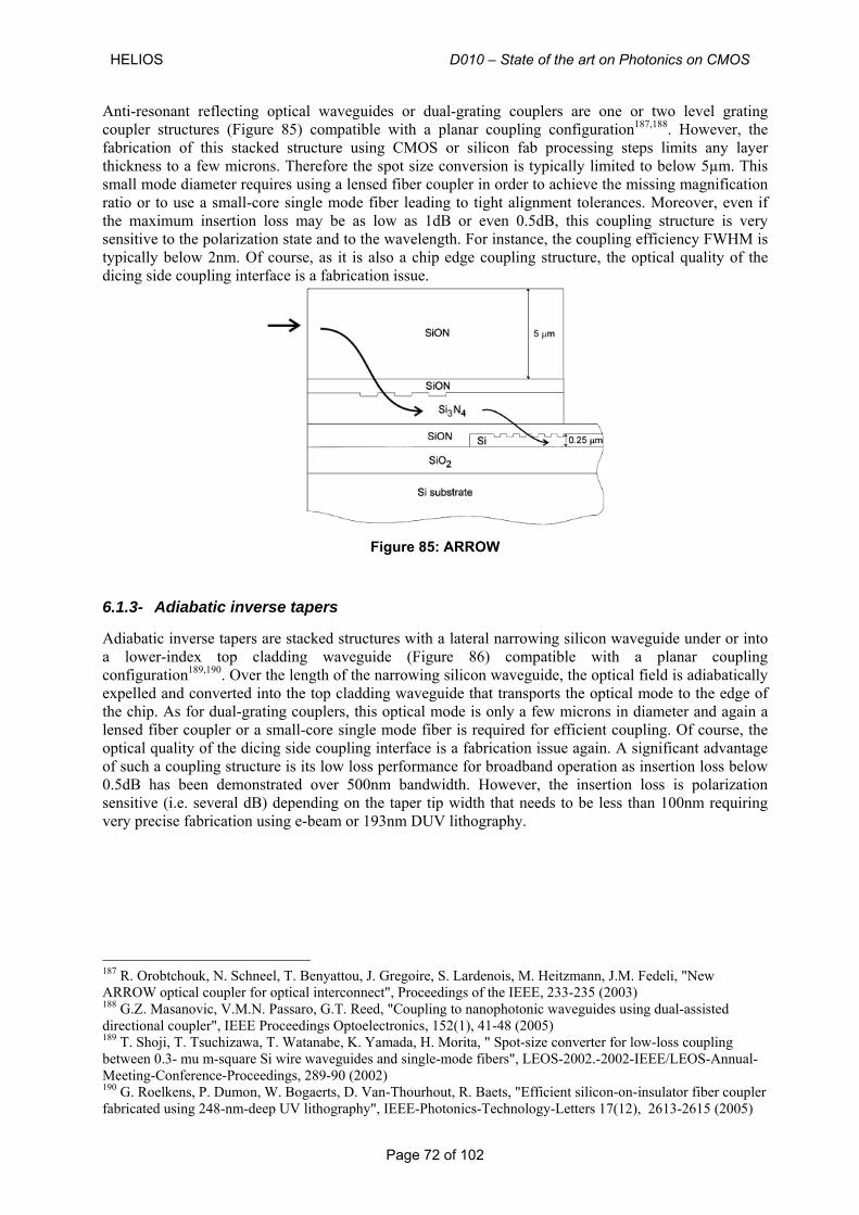
HELIOS D010 – State of the art on Photonics on CMOS
Page 72 of 102
Anti-resonant reflecting optical waveguides or dual-grating couplers are one or two level grating coupler structures (Figure 85) compatible with a planar coupling configuration187,188. However, the fabrication of this stacked structure using CMOS or silicon fab processing steps limits any layer thickness to a few microns. Therefore the spot size conversion is typically limited to below 5µm. This small mode diameter requires using a lensed fiber coupler in order to achieve the missing magnification ratio or to use a small-core single mode fiber leading to tight alignment tolerances. Moreover, even if the maximum insertion loss may be as low as 1dB or even 0.5dB, this coupling structure is very sensitive to the polarization state and to the wavelength. For instance, the coupling efficiency FWHM is typically below 2nm. Of course, as it is also a chip edge coupling structure, the optical quality of the dicing side coupling interface is a fabrication issue.
Figure 85: ARROW
6.1.3- Adiabatic inverse tapers
Adiabatic inverse tapers are stacked structures with a lateral narrowing silicon waveguide under or into a lower-index top cladding waveguide (Figure 86) compatible with a planar coupling configuration189,190. Over the length of the narrowing silicon waveguide, the optical field is adiabatically expelled and converted into the top cladding waveguide that transports the optical mode to the edge of the chip. As for dual-grating couplers, this optical mode is only a few microns in diameter and again a lensed fiber coupler or a small-core single mode fiber is required for efficient coupling. Of course, the optical quality of the dicing side coupling interface is a fabrication issue again. A significant advantage of such a coupling structure is its low loss performance for broadband operation as insertion loss below 0.5dB has been demonstrated over 500nm bandwidth. However, the insertion loss is polarization sensitive (i.e. several dB) depending on the taper tip width that needs to be less than 100nm requiring very precise fabrication using e-beam or 193nm DUV lithography.
187 R. Orobtchouk, N. Schneel, T. Benyattou, J. Gregoire, S. Lardenois, M. Heitzmann, J.M. Fedeli, "New ARROW optical coupler for optical interconnect", Proceedings of the IEEE, 233-235 (2003) 188 G.Z. Masanovic, V.M.N. Passaro, G.T. Reed, "Coupling to nanophotonic waveguides using dual-assisted directional coupler", IEEE Proceedings Optoelectronics, 152(1), 41-48 (2005) 189 T. Shoji, T. Tsuchizawa, T. Watanabe, K. Yamada, H. Morita, " Spot-size converter for low-loss coupling between 0.3- mu m-square Si wire waveguides and single-mode fibers", LEOS-2002.-2002-IEEE/LEOS-Annual-Meeting-Conference-Proceedings, 289-90 (2002) 190 G. Roelkens, P. Dumon, W. Bogaerts, D. Van-Thourhout, R. Baets, "Efficient silicon-on-insulator fiber coupler fabricated using 248-nm-deep UV lithography", IEEE-Photonics-Technology-Letters 17(12), 2613-2615 (2005)
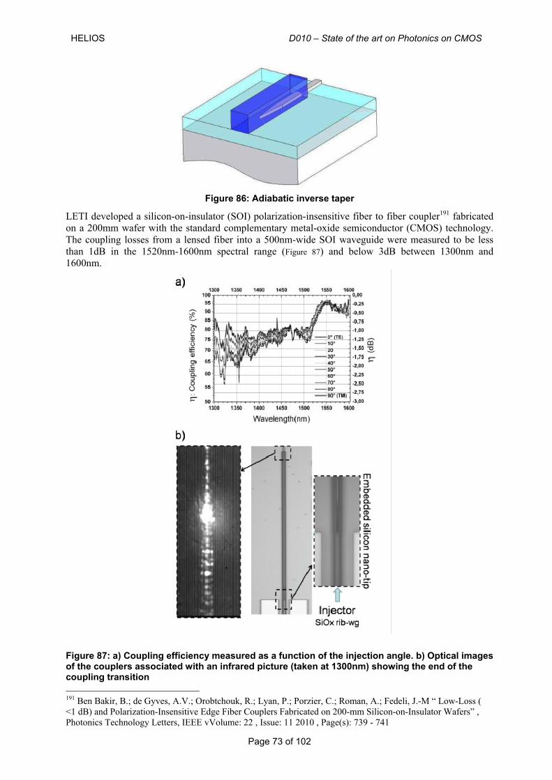
HELIOS D010 – State of the art on Photonics on CMOS
Page 73 of 102
Figure 86: Adiabatic inverse taper
LETI developed a silicon-on-insulator (SOI) polarization-insensitive fiber to fiber coupler191 fabricated on a 200mm wafer with the standard complementary metal-oxide semiconductor (CMOS) technology. The coupling losses from a lensed fiber into a 500nm-wide SOI waveguide were measured to be less than 1dB in the 1520nm-1600nm spectral range (Figure 87) and below 3dB between 1300nm and 1600nm.
Figure 87: a) Coupling efficiency measured as a function of the injection angle. b) Optical images of the couplers associated with an infrared picture (taken at 1300nm) showing the end of the coupling transition 191 Ben Bakir, B.; de Gyves, A.V.; Orobtchouk, R.; Lyan, P.; Porzier, C.; Roman, A.; Fedeli, J.-M “ Low-Loss ( <1 dB) and Polarization-Insensitive Edge Fiber Couplers Fabricated on 200-mm Silicon-on-Insulator Wafers” , Photonics Technology Letters, IEEE vVolume: 22 , Issue: 11 2010 , Page(s): 739 - 741
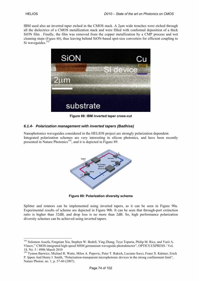
HELIOS D010 – State of the art on Photonics on CMOS
Page 74 of 102
IBM used also an inverted taper etched in the CMOS stack. A 2μm wide trenches were etched through all the dielectrics of a CMOS metallization stack and were filled with conformal deposition of a thick SiON film . Finally, the film was removed from the copper metallization by a CMP process and wet cleaning steps (Figure 88), thus leaving behind SiON-based spot-size converters for efficient coupling to Si waveguides.192
Figure 88: IBM inverted taper cross-cut
6.1.4- Polarization management with inverted tapers (Badhise)
Nanophotonics waveguides considered in the HELIOS project are strongly polarization dependent. Integrated polarization schemes are very interesting in silicon photonics, and have been recently presented in Nature Photonics193, and it is depicted in Figure 89.
Figure 89: Polarization diversity scheme
Splitter and rotators can be implemented using inverted tapers, as it can be seen in Figure 90a. Experimental results of scheme are depicted in Figure 90b. It can be seen that through-port extinction ratio is higher than 32dB, and drop loss is no more than 2dB. So, high performance polarization diversity schemes can be achieved using inverted tapers.
192 Solomon Assefa, Fengnian Xia, Stephen W. Bedell, Ying Zhang, Teya Topuria, Philip M. Rice, and Yurii A. Vlasov,” CMOS-integrated high-speed MSM germanium waveguide photodetector”, OPTICS EXPRESS / Vol. 18, No. 5 / 4986 March 2010 193 Tymon Barwicz, Michael R. Watts, Milos A. Popovic, Peter T. Rakich, Luciano Socci, Franz X. Kärtner, Erich P. Ippen And Henry I. Smith, “Polarization-transparent microphotonic devices in the strong confinement limit“, Nature Photon. no. 1, p. 57-60 (2007).
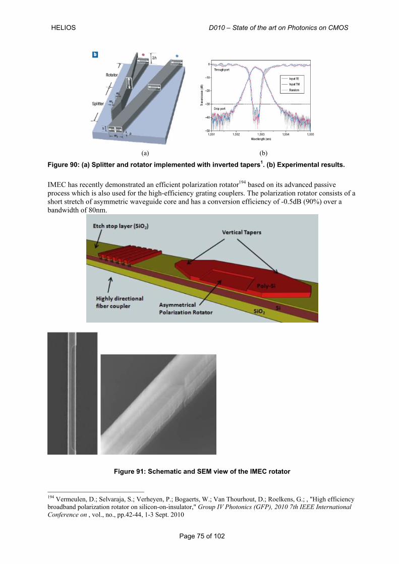
HELIOS D010 – State of the art on Photonics on CMOS
Page 75 of 102
(a) (b)
Figure 90: (a) Splitter and rotator implemented with inverted tapers1. (b) Experimental results.
IMEC has recently demonstrated an efficient polarization rotator194 based on its advanced passive process which is also used for the high-efficiency grating couplers. The polarization rotator consists of a short stretch of asymmetric waveguide core and has a conversion efficiency of -0.5dB (90%) over a bandwidth of 80nm.
Figure 91: Schematic and SEM view of the IMEC rotator 194 Vermeulen, D.; Selvaraja, S.; Verheyen, P.; Bogaerts, W.; Van Thourhout, D.; Roelkens, G.; , "High efficiency broadband polarization rotator on silicon-on-insulator," Group IV Photonics (GFP), 2010 7th IEEE International Conference on , vol., no., pp.42-44, 1-3 Sept. 2010
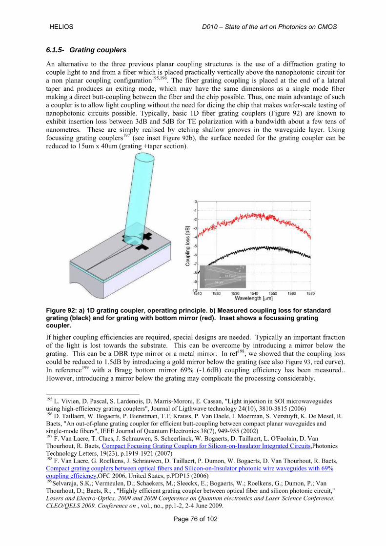
HELIOS D010 – State of the art on Photonics on CMOS
Page 76 of 102
6.1.5- Grating couplers
An alternative to the three previous planar coupling structures is the use of a diffraction grating to couple light to and from a fiber which is placed practically vertically above the nanophotonic circuit for a non planar coupling configuration195,196. The fiber grating coupling is placed at the end of a lateral taper and produces an exiting mode, which may have the same dimensions as a single mode fiber making a direct butt-coupling between the fiber and the chip possible. Thus, one main advantage of such a coupler is to allow light coupling without the need for dicing the chip that makes wafer-scale testing of nanophotonic circuits possible. Typically, basic 1D fiber grating couplers (Figure 92) are known to exhibit insertion loss between 3dB and 5dB for TE polarization with a bandwidth about a few tens of nanometres. These are simply realised by etching shallow grooves in the waveguide layer. Using focussing grating couplers197 (see inset Figure 92b), the surface needed for the grating coupler can be reduced to 15um x 40um (grating +taper section).
Figure 92: a) 1D grating coupler, operating principle. b) Measured coupling loss for standard grating (black) and for grating with bottom mirror (red). Inset shows a focussing grating coupler.
If higher coupling efficiencies are required, special designs are needed. Typically an important fraction of the light is lost towards the substrate. This can be overcome by introducing a mirror below the grating. This can be a DBR type mirror or a metal mirror. In ref198, we showed that the coupling loss could be reduced to 1.5dB by introducing a gold mirror below the grating (see also Figure 93, red curve). In reference199 with a Bragg bottom mirror 69% (-1.6dB) coupling efficiency has been measured.. However, introducing a mirror below the grating may complicate the processing considerably.
195 L. Vivien, D. Pascal, S. Lardenois, D. Marris-Moroni, E. Cassan, "Light injection in SOI microwaveguides using high-efficiency grating couplers", Journal of Ligthwave technology 24(10), 3810-3815 (2006) 196 D. Taillaert, W. Bogaerts, P. Bienstman, T.F. Krauss, P. Van Daele, I. Moerman, S. Verstuyft, K. De Mesel, R. Baets, "An out-of-plane grating coupler for efficient butt-coupling between compact planar waveguides and single-mode fibers", IEEE Journal of Quantum Electronics 38(7), 949-955 (2002) 197 F. Van Laere, T. Claes, J. Schrauwen, S. Scheerlinck, W. Bogaerts, D. Taillaert, L. O'Faolain, D. Van Thourhout, R. Baets, Compact Focusing Grating Couplers for Silicon-on-Insulator Integrated Circuits,Photonics Technology Letters, 19(23), p.1919-1921 (2007) 198 F. Van Laere, G. Roelkens, J. Schrauwen, D. Taillaert, P. Dumon, W. Bogaerts, D. Van Thourhout, R. Baets, Compact grating couplers between optical fibers and Silicon-on-Insulator photonic wire waveguides with 69% coupling efficiency,OFC 2006, United States, p.PDP15 (2006) 199Selvaraja, S.K.; Vermeulen, D.; Schaekers, M.; Sleeckx, E.; Bogaerts, W.; Roelkens, G.; Dumon, P.; Van Thourhout, D.; Baets, R.; , "Highly efficient grating coupler between optical fiber and silicon photonic circuit," Lasers and Electro-Optics, 2009 and 2009 Conference on Quantum electronics and Laser Science Conference. CLEO/QELS 2009. Conference on , vol., no., pp.1-2, 2-4 June 2009.
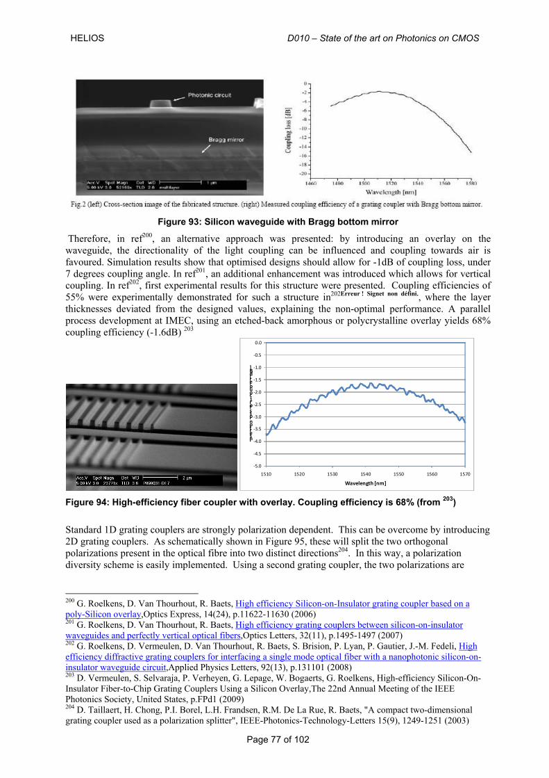
HELIOS D010 – State of the art on Photonics on CMOS
Page 77 of 102
Figure 93: Silicon waveguide with Bragg bottom mirror
Therefore, in ref200, an alternative approach was presented: by introducing an overlay on the waveguide, the directionality of the light coupling can be influenced and coupling towards air is favoured. Simulation results show that optimised designs should allow for -1dB of coupling loss, under 7 degrees coupling angle. In ref201, an additional enhancement was introduced which allows for vertical coupling. In ref202, first experimental results for this structure were presented. Coupling efficiencies of 55% were experimentally demonstrated for such a structure in202Erreur ! Signet non défini., where the layer thicknesses deviated from the designed values, explaining the non-optimal performance. A parallel process development at IMEC, using an etched-back amorphous or polycrystalline overlay yields 68% coupling efficiency (-1.6dB) 203
‐5.0
‐4.5
‐4.0
‐3.5
‐3.0
‐2.5
‐2.0
‐1.5
‐1.0
‐0.5
0.0
1510 1520 1530 1540 1550 1560 1570
Insertion loss for 1 coupler [dB]
Wavelength [nm] Figure 94: High-efficiency fiber coupler with overlay. Coupling efficiency is 68% (from 203) Standard 1D grating couplers are strongly polarization dependent. This can be overcome by introducing 2D grating couplers. As schematically shown in Figure 95, these will split the two orthogonal polarizations present in the optical fibre into two distinct directions204. In this way, a polarization diversity scheme is easily implemented. Using a second grating coupler, the two polarizations are
200 G. Roelkens, D. Van Thourhout, R. Baets, High efficiency Silicon-on-Insulator grating coupler based on a poly-Silicon overlay,Optics Express, 14(24), p.11622-11630 (2006) 201 G. Roelkens, D. Van Thourhout, R. Baets, High efficiency grating couplers between silicon-on-insulator waveguides and perfectly vertical optical fibers,Optics Letters, 32(11), p.1495-1497 (2007) 202 G. Roelkens, D. Vermeulen, D. Van Thourhout, R. Baets, S. Brision, P. Lyan, P. Gautier, J.-M. Fedeli, High efficiency diffractive grating couplers for interfacing a single mode optical fiber with a nanophotonic silicon-on-insulator waveguide circuit,Applied Physics Letters, 92(13), p.131101 (2008) 203 D. Vermeulen, S. Selvaraja, P. Verheyen, G. Lepage, W. Bogaerts, G. Roelkens, High-efficiency Silicon-On-Insulator Fiber-to-Chip Grating Couplers Using a Silicon Overlay,The 22nd Annual Meeting of the IEEE Photonics Society, United States, p.FPd1 (2009) 204 D. Taillaert, H. Chong, P.I. Borel, L.H. Frandsen, R.M. De La Rue, R. Baets, "A compact two-dimensional grating coupler used as a polarization splitter", IEEE-Photonics-Technology-Letters 15(9), 1249-1251 (2003)
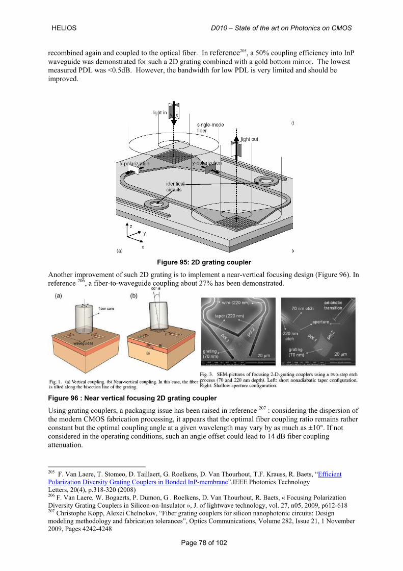
HELIOS D010 – State of the art on Photonics on CMOS
Page 78 of 102
recombined again and coupled to the optical fiber. In reference205, a 50% coupling efficiency into InP waveguide was demonstrated for such a 2D grating combined with a gold bottom mirror. The lowest measured PDL was <0.5dB. However, the bandwidth for low PDL is very limited and should be improved.
Figure 95: 2D grating coupler
Another improvement of such 2D grating is to implement a near-vertical focusing design (Figure 96). In reference 206, a fiber-to-waveguide coupling about 27% has been demonstrated.
Figure 96 : Near vertical focusing 2D grating coupler
Using grating couplers, a packaging issue has been raised in reference 207 : considering the dispersion of the modern CMOS fabrication processing, it appears that the optimal fiber coupling ratio remains rather constant but the optimal coupling angle at a given wavelength may vary by as much as ±10°. If not considered in the operating conditions, such an angle offset could lead to 14 dB fiber coupling attenuation.
205 F. Van Laere, T. Stomeo, D. Taillaert, G. Roelkens, D. Van Thourhout, T.F. Krauss, R. Baets, “Efficient Polarization Diversity Grating Couplers in Bonded InP-membrane”,IEEE Photonics Technology Letters, 20(4), p.318-320 (2008) 206 F. Van Laere, W. Bogaerts, P. Dumon, G . Roelkens, D. Van Thourhout, R. Baets, « Focusing Polarization Diversity Grating Couplers in Silicon-on-Insulator », J. of lightwave technology, vol. 27, n05, 2009, p612-618 207 Christophe Kopp, Alexei Chelnokov, “Fiber grating couplers for silicon nanophotonic circuits: Design modeling methodology and fabrication tolerances”, Optics Communications, Volume 282, Issue 21, 1 November 2009, Pages 4242-4248
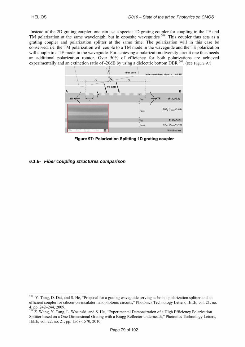
HELIOS D010 – State of the art on Photonics on CMOS
Page 79 of 102
Instead of the 2D grating coupler, one can use a special 1D grating coupler for coupling in the TE and TM polarization at the same wavelength, but in opposite waveguides 208. This coupler thus acts as a grating coupler and polarization splitter at the same time. The polarization will in this case be conserved, i.e. the TM polarization will couple to a TM mode in the waveguide and the TE polarization will couple to a TE mode in the waveguide. For achieving a polarization diversity circuit one thus needs an additional polarization rotator. Over 50% of efficiency for both polarizations are achieved experimentally and an extinction ratio of -20dB by using a dielectric bottom DBR 209. (see Figure 97)
Figure 97: Polarization Splitting 1D grating coupler
6.1.6- Fiber coupling structures comparison
208 Y. Tang, D. Dai, and S. He, “Proposal for a grating waveguide serving as both a polarization splitter and an efficient coupler for silicon-on-insulator nanophotonic circuits,” Photonics Technology Letters, IEEE, vol. 21, no. 4, pp. 242–244, 2009. 209 Z. Wang, Y. Tang, L. Wosinski, and S. He, “Experimental Demonstration of a High Efficiency Polarization Splitter based on a One-Dimensional Grating with a Bragg Reflector underneath,” Photonics Technology Letters, IEEE, vol. 22, no. 21, pp. 1568-1570, 2010.
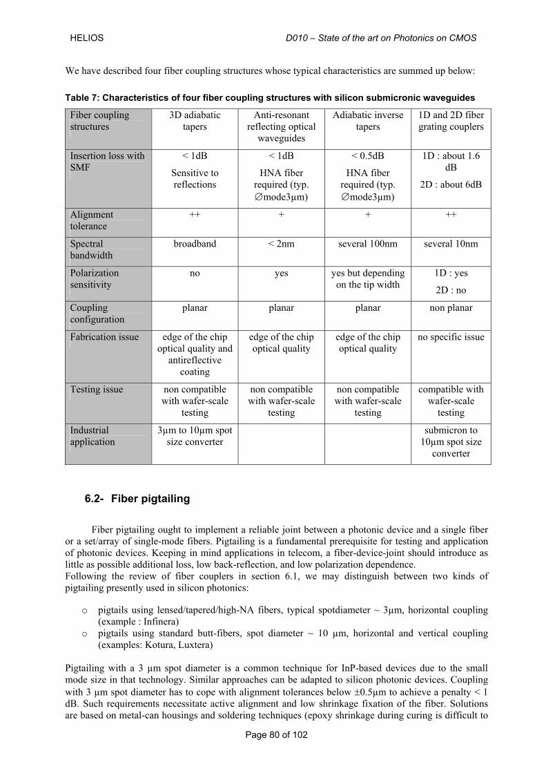
HELIOS D010 – State of the art on Photonics on CMOS
Page 80 of 102
We have described four fiber coupling structures whose typical characteristics are summed up below:
Table 7: Characteristics of four fiber coupling structures with silicon submicronic waveguides
Fiber coupling structures
3D adiabatic tapers
Anti-resonant reflecting optical
waveguides
Adiabatic inverse tapers
1D and 2D fiber grating couplers
Insertion loss with SMF
< 1dB
Sensitive to reflections
< 1dB
HNA fiber required (typ. ∅mode3µm)
< 0.5dB
HNA fiber required (typ. ∅mode3µm)
1D : about 1.6 dB
2D : about 6dB
Alignment tolerance
++ + + ++
Spectral bandwidth
broadband < 2nm several 100nm several 10nm
Polarization sensitivity
no yes yes but depending on the tip width
1D : yes
2D : no
Coupling configuration
planar planar planar non planar
Fabrication issue edge of the chip optical quality and
antireflective coating
edge of the chip optical quality
edge of the chip optical quality
no specific issue
Testing issue non compatible with wafer-scale
testing
non compatible with wafer-scale
testing
non compatible with wafer-scale
testing
compatible with wafer-scale
testing
Industrial application
3µm to 10µm spot size converter
submicron to 10µm spot size
converter
6.2- Fiber pigtailing
Fiber pigtailing ought to implement a reliable joint between a photonic device and a single fiber
or a set/array of single-mode fibers. Pigtailing is a fundamental prerequisite for testing and application of photonic devices. Keeping in mind applications in telecom, a fiber-device-joint should introduce as little as possible additional loss, low back-reflection, and low polarization dependence. Following the review of fiber couplers in section 6.1, we may distinguish between two kinds of pigtailing presently used in silicon photonics:
o pigtails using lensed/tapered/high-NA fibers, typical spotdiameter ~ 3µm, horizontal coupling (example : Infinera)
o pigtails using standard butt-fibers, spot diameter ~ 10 µm, horizontal and vertical coupling (examples: Kotura, Luxtera)
Pigtailing with a 3 µm spot diameter is a common technique for InP-based devices due to the small mode size in that technology. Similar approaches can be adapted to silicon photonic devices. Coupling with 3 µm spot diameter has to cope with alignment tolerances below ±0.5µm to achieve a penalty < 1 dB. Such requirements necessitate active alignment and low shrinkage fixation of the fiber. Solutions are based on metal-can housings and soldering techniques (epoxy shrinkage during curing is difficult to
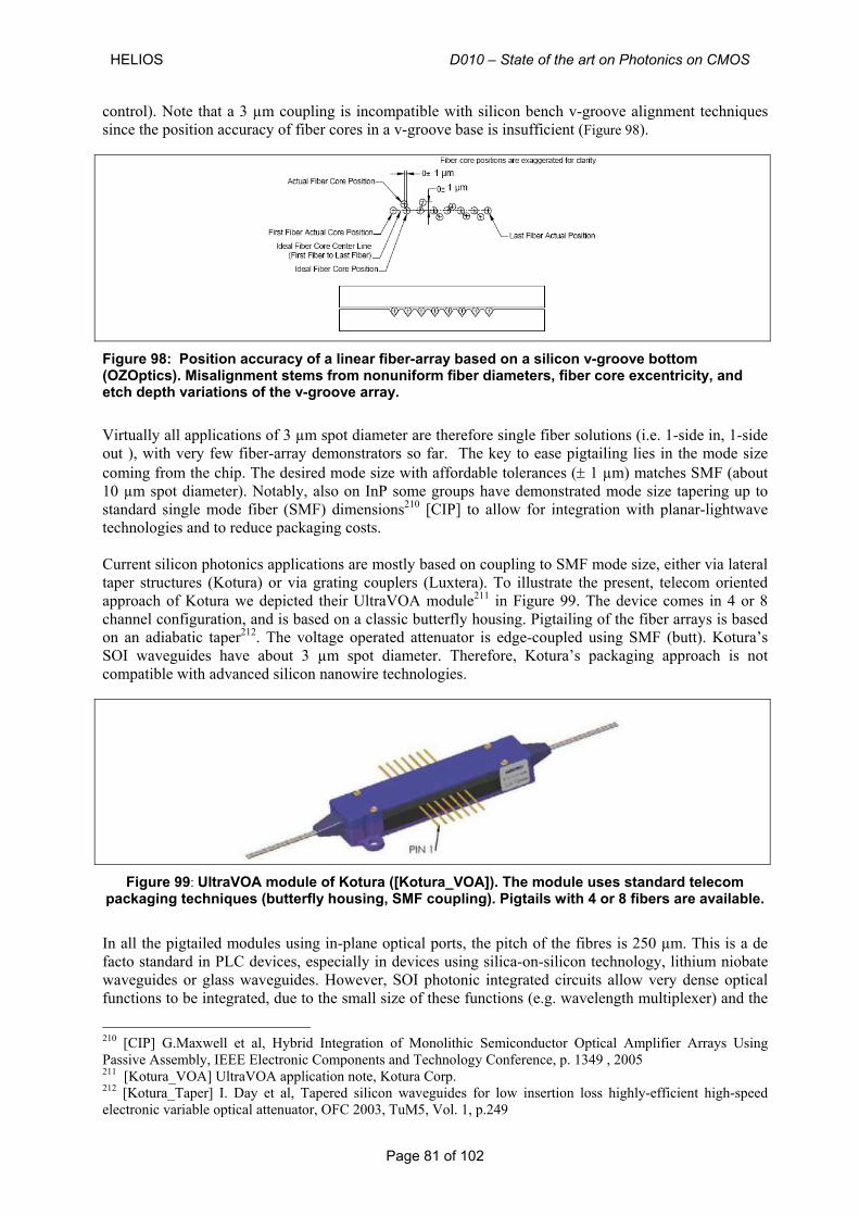
HELIOS D010 – State of the art on Photonics on CMOS
Page 81 of 102
control). Note that a 3 µm coupling is incompatible with silicon bench v-groove alignment techniques since the position accuracy of fiber cores in a v-groove base is insufficient (Figure 98).
Figure 98: Position accuracy of a linear fiber-array based on a silicon v-groove bottom (OZOptics). Misalignment stems from nonuniform fiber diameters, fiber core excentricity, and etch depth variations of the v-groove array.
Virtually all applications of 3 µm spot diameter are therefore single fiber solutions (i.e. 1-side in, 1-side out ), with very few fiber-array demonstrators so far. The key to ease pigtailing lies in the mode size coming from the chip. The desired mode size with affordable tolerances (± 1 µm) matches SMF (about 10 µm spot diameter). Notably, also on InP some groups have demonstrated mode size tapering up to standard single mode fiber (SMF) dimensions210 [CIP] to allow for integration with planar-lightwave technologies and to reduce packaging costs. Current silicon photonics applications are mostly based on coupling to SMF mode size, either via lateral taper structures (Kotura) or via grating couplers (Luxtera). To illustrate the present, telecom oriented approach of Kotura we depicted their UltraVOA module211 in Figure 99. The device comes in 4 or 8 channel configuration, and is based on a classic butterfly housing. Pigtailing of the fiber arrays is based on an adiabatic taper212. The voltage operated attenuator is edge-coupled using SMF (butt). Kotura’s SOI waveguides have about 3 µm spot diameter. Therefore, Kotura’s packaging approach is not compatible with advanced silicon nanowire technologies.
Figure 99: UltraVOA module of Kotura ([Kotura_VOA]). The module uses standard telecom
packaging techniques (butterfly housing, SMF coupling). Pigtails with 4 or 8 fibers are available.
In all the pigtailed modules using in-plane optical ports, the pitch of the fibres is 250 µm. This is a de facto standard in PLC devices, especially in devices using silica-on-silicon technology, lithium niobate waveguides or glass waveguides. However, SOI photonic integrated circuits allow very dense optical functions to be integrated, due to the small size of these functions (e.g. wavelength multiplexer) and the
210 [CIP] G.Maxwell et al, Hybrid Integration of Monolithic Semiconductor Optical Amplifier Arrays Using Passive Assembly, IEEE Electronic Components and Technology Conference, p. 1349 , 2005 211 [Kotura_VOA] UltraVOA application note, Kotura Corp. 212 [Kotura_Taper] I. Day et al, Tapered silicon waveguides for low insertion loss highly-efficient high-speed electronic variable optical attenuator, OFC 2003, TuM5, Vol. 1, p.249
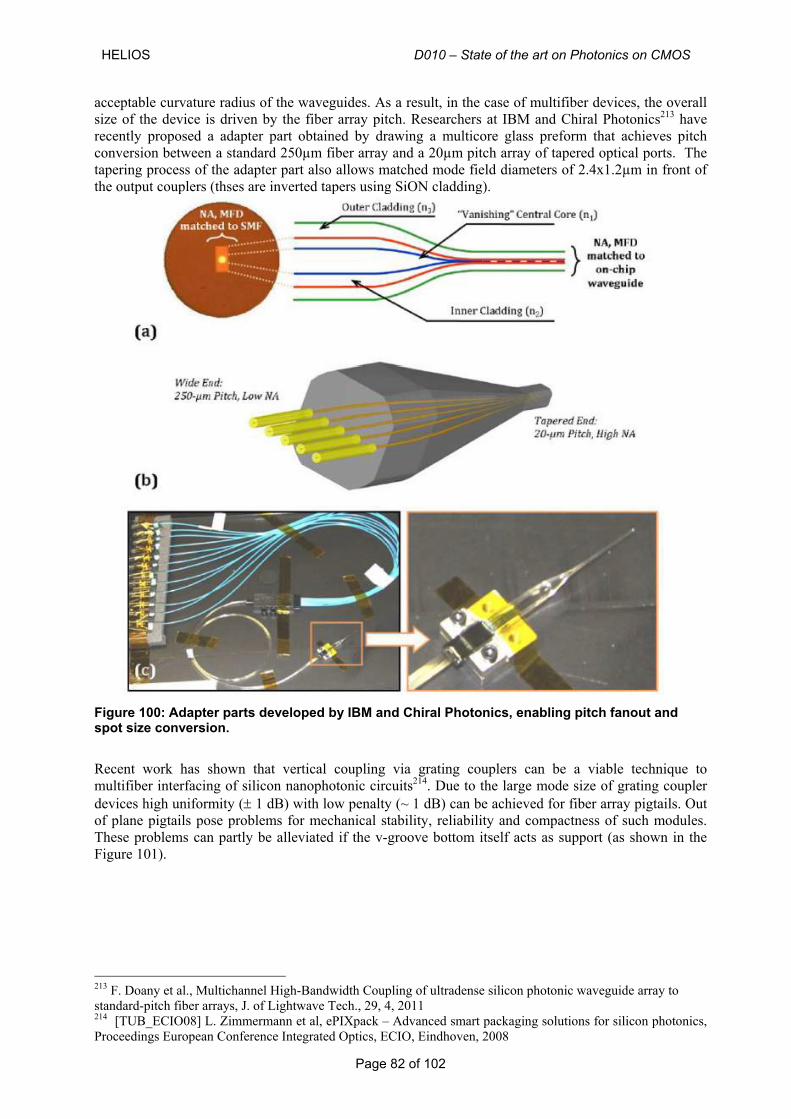
HELIOS D010 – State of the art on Photonics on CMOS
Page 82 of 102
acceptable curvature radius of the waveguides. As a result, in the case of multifiber devices, the overall size of the device is driven by the fiber array pitch. Researchers at IBM and Chiral Photonics213 have recently proposed a adapter part obtained by drawing a multicore glass preform that achieves pitch conversion between a standard 250µm fiber array and a 20µm pitch array of tapered optical ports. The tapering process of the adapter part also allows matched mode field diameters of 2.4x1.2µm in front of the output couplers (thses are inverted tapers using SiON cladding).
Figure 100: Adapter parts developed by IBM and Chiral Photonics, enabling pitch fanout and spot size conversion. Recent work has shown that vertical coupling via grating couplers can be a viable technique to multifiber interfacing of silicon nanophotonic circuits214. Due to the large mode size of grating coupler devices high uniformity (± 1 dB) with low penalty (~ 1 dB) can be achieved for fiber array pigtails. Out of plane pigtails pose problems for mechanical stability, reliability and compactness of such modules. These problems can partly be alleviated if the v-groove bottom itself acts as support (as shown in the Figure 101).
213 F. Doany et al., Multichannel High-Bandwidth Coupling of ultradense silicon photonic waveguide array to standard-pitch fiber arrays, J. of Lightwave Tech., 29, 4, 2011 214 [TUB_ECIO08] L. Zimmermann et al, ePIXpack – Advanced smart packaging solutions for silicon photonics, Proceedings European Conference Integrated Optics, ECIO, Eindhoven, 2008
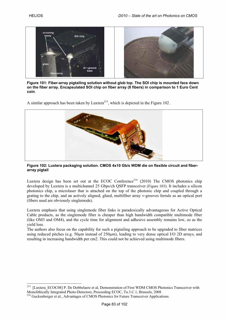
HELIOS D010 – State of the art on Photonics on CMOS
Page 83 of 102
Figure 101: Fiber-array pigtailing solution without glob top. The SOI chip is mounted face down on the fiber array. Encapsulated SOI chip on fiber array (8 fibers) in comparison to 1 Euro Cent coin.
A similar approach has been taken by Luxtera215, which is depicted in the Figure 102 .
Figure 102: Luxtera packaging solution. CMOS 4x10 Gb/s WDM die on flexible circuit and fiber-array pigtail Luxtera design has been set out at the ECOC Conference216 (2010) The CMOS photonics chip developed by Luxtera is a multichannel 25 Gbps/ch QSFP transceiver (Figure 103). It includes a silicon photonics chip, a microlaser that is attached on the top of the photonic chip and coupled through a grating to the chip, and an actively aligned, glued, multifiber array v-grooves ferrule as an optical port (fibers used are obviously singlemode). Luxtera emphasis that using singlemode fiber links is paradoxically advantageous for Active Optical Cable products, as the singlemode fiber is cheaper than high bandwidth compatible multimode fiber (like OM3 and OM4), and the cycle time for alignment and adhesive assembly remains low, so as the yield loss. The authors also focus on the capability for such a pigtailing approach to be upgraded to fiber matrices using reduced pitches (e.g. 50µm instead of 250µm), leading to very dense optical I/O 2D arrays, and resulting in increasing bandwidth per cm2. This could not be achieved using multimode fibers.
215 [Luxtera_ECOC08] P. De Dobbelaere et al, Demonstration of First WDM CMOS Photonics Transceiver with Monolithically Integrated Photo-Detectors, Proceeding ECOC, Tu.3.C.1, Brussels, 2008 216 Guckenberger et al., Advantages of CMOS Photonics for Future Transceiver Applications.
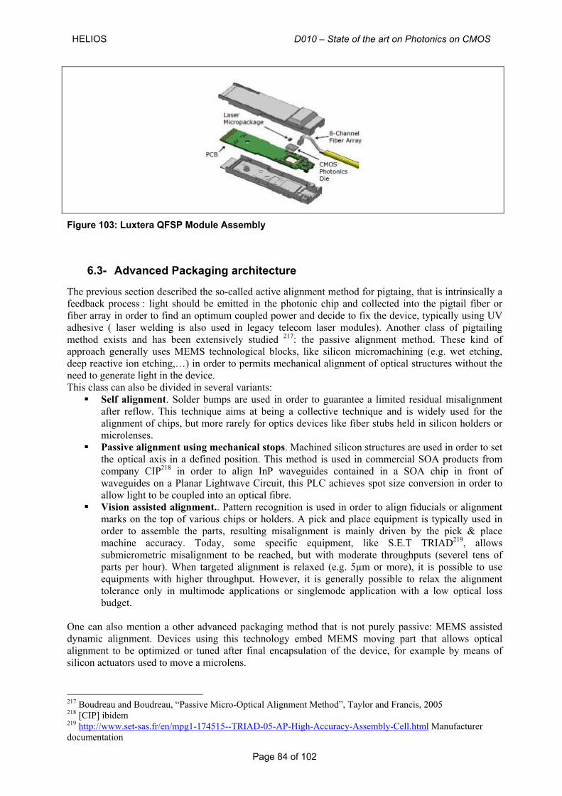
HELIOS D010 – State of the art on Photonics on CMOS
Page 84 of 102
Figure 103: Luxtera QFSP Module Assembly
6.3- Advanced Packaging architecture
The previous section described the so-called active alignment method for pigtaing, that is intrinsically a feedback process : light should be emitted in the photonic chip and collected into the pigtail fiber or fiber array in order to find an optimum coupled power and decide to fix the device, typically using UV adhesive ( laser welding is also used in legacy telecom laser modules). Another class of pigtailing method exists and has been extensively studied 217: the passive alignment method. These kind of approach generally uses MEMS technological blocks, like silicon micromachining (e.g. wet etching, deep reactive ion etching,…) in order to permits mechanical alignment of optical structures without the need to generate light in the device. This class can also be divided in several variants:
Self alignment. Solder bumps are used in order to guarantee a limited residual misalignment after reflow. This technique aims at being a collective technique and is widely used for the alignment of chips, but more rarely for optics devices like fiber stubs held in silicon holders or microlenses.
Passive alignment using mechanical stops. Machined silicon structures are used in order to set the optical axis in a defined position. This method is used in commercial SOA products from company CIP218 in order to align InP waveguides contained in a SOA chip in front of waveguides on a Planar Lightwave Circuit, this PLC achieves spot size conversion in order to allow light to be coupled into an optical fibre.
Vision assisted alignment.. Pattern recognition is used in order to align fiducials or alignment marks on the top of various chips or holders. A pick and place equipment is typically used in order to assemble the parts, resulting misalignment is mainly driven by the pick & place machine accuracy. Today, some specific equipment, like S.E.T TRIAD219, allows submicrometric misalignment to be reached, but with moderate throughputs (severel tens of parts per hour). When targeted alignment is relaxed (e.g. 5µm or more), it is possible to use equipments with higher throughput. However, it is generally possible to relax the alignment tolerance only in multimode applications or singlemode application with a low optical loss budget.
One can also mention a other advanced packaging method that is not purely passive: MEMS assisted dynamic alignment. Devices using this technology embed MEMS moving part that allows optical alignment to be optimized or tuned after final encapsulation of the device, for example by means of silicon actuators used to move a microlens.
217 Boudreau and Boudreau, “Passive Micro-Optical Alignment Method”, Taylor and Francis, 2005 218 [CIP] ibidem 219 http://www.set-sas.fr/en/mpg1-174515--TRIAD-05-AP-High-Accuracy-Assembly-Cell.html Manufacturer documentation
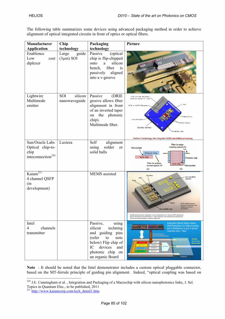
HELIOS D010 – State of the art on Photonics on CMOS
Page 85 of 102
The following table summarizes some devices using advanced packaging method in order to achieve alignment of optical integrated circuits in front of optics or optical fibers. Manufacturer Application
Chip technology
Packaging technology
Picture
Enablence Low cost diplexer
Large guide (3µm) SOI
Passive (optical chip is flip-chipped onto a silicon bench, fiber is passively aligned into a v-groove
Lightwire Multimode emitter
SOI silicon nanowaveguide
Passive (DRIE groove allows fiber alignment in front of an inverted taper on the photonic chip). Multimode fiber.
Sun/Oracle Labs Optical chip-to-chip inteconnection220
Luxtera Self alignment using solder or solid balls
Kaiam221 4 channel QSFP (in development)
MEMS assisted
Intel 4 channels transmitter
Passive, using silicon techning and guiding pins (refer to note below) Flip chip of IC devices and photonic chip on an organic Board
Note : It should be noted that the Intel demonstrator includes a custom optical pluggable connector, based on the MT-ferrule principle of guiding pin alignment. Indeed, “optical coupling was based on 220 J.E. Cunningham et al. , Integration and Packaging of a Macrochip with silicon nanophotonics links, J. Sel. Topics in Quantum Elec., to be published, 2011 221 http://www.kaiamcorp.com/tech_detail1.htm
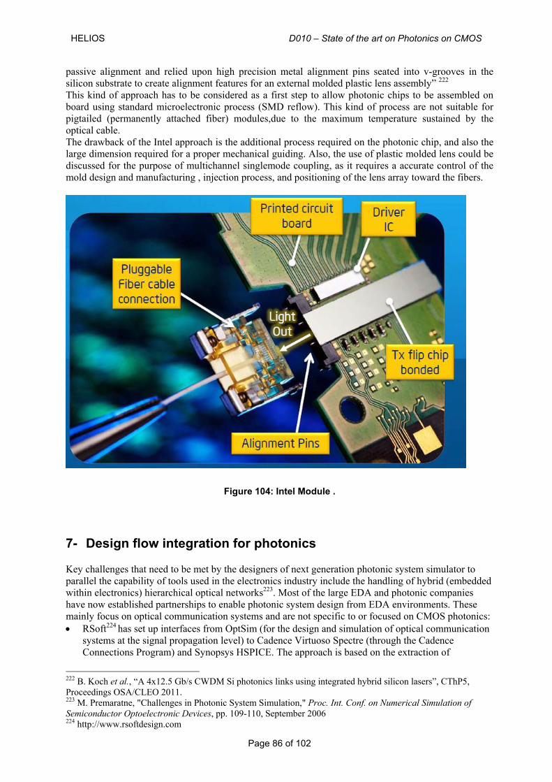
HELIOS D010 – State of the art on Photonics on CMOS
Page 86 of 102
passive alignment and relied upon high precision metal alignment pins seated into v-grooves in the silicon substrate to create alignment features for an external molded plastic lens assembly” 222 This kind of approach has to be considered as a first step to allow photonic chips to be assembled on board using standard microelectronic process (SMD reflow). This kind of process are not suitable for pigtailed (permanently attached fiber) modules,due to the maximum temperature sustained by the optical cable. The drawback of the Intel approach is the additional process required on the photonic chip, and also the large dimension required for a proper mechanical guiding. Also, the use of plastic molded lens could be discussed for the purpose of multichannel singlemode coupling, as it requires a accurate control of the mold design and manufacturing , injection process, and positioning of the lens array toward the fibers.
Figure 104: Intel Module .
7- Design flow integration for photonics
Key challenges that need to be met by the designers of next generation photonic system simulator to parallel the capability of tools used in the electronics industry include the handling of hybrid (embedded within electronics) hierarchical optical networks223. Most of the large EDA and photonic companies have now established partnerships to enable photonic system design from EDA environments. These mainly focus on optical communication systems and are not specific to or focused on CMOS photonics: • RSoft224 has set up interfaces from OptSim (for the design and simulation of optical communication
systems at the signal propagation level) to Cadence Virtuoso Spectre (through the Cadence Connections Program) and Synopsys HSPICE. The approach is based on the extraction of
222 B. Koch et al., “A 4x12.5 Gb/s CWDM Si photonics links using integrated hybrid silicon lasers”, CThP5, Proceedings OSA/CLEO 2011. 223 M. Premaratne, "Challenges in Photonic System Simulation," Proc. Int. Conf. on Numerical Simulation of Semiconductor Optoelectronic Devices, pp. 109-110, September 2006 224 http://www.rsoftdesign.com
HELIOS D010 – State of the art on Photonics on CMOS
Page 87 of 102
parameters for predefined behavioural models. A Matlab interface also enables the development of custom user models.
• VPI Photonics225 uses the co-simulation approach in collaboration with Agilent-ADS. Here, to achieve in-depth understanding of the interactions between the electronic and photonic parts of a link, full electronic circuit models are incorporated directly into the optical systems simulation. This is mainly achieved via Agilent's ADS high-frequency electronic circuit design tools and component libraries.
• Matlab/Simulink226 has also been used by (among others) Yokogawa Electric to model a multiplexer/demultiplexer and error-correction codes. After converting the components manually into HDL, Mentor Graphics227 ModelSim was used to verify the control specifications. It is possible in this way to simulate the model, verify the processing functionalities of electronic circuits (here an FPGA) and troubleshoot design errors in a fast design loop.
• For the design houses, Luxtera have also developed a model library228 containing a set of optical elements (I/Os, modulators, detectors, waveguides, etc…) as well as accompanying models, and automated verification (design rules, layout-vs-schematic) and full system simulation. This is a consolidation of established and academic approaches such as that proposed by INL229,230.
8- Convergence Photonics- Electronics
Apart from the flip-chip technique where two separate dies are bonded using metallic bonding, the integration of photonics devices on an electronic chip can be envisioned by different means summarized in Figure 105.
225 http://www.vpiphotonics.com 226 http://www.mathworks.com 227 http://www.mentor.com/ 228 T. Pinguet et al., "Monolithically Integrated High-Speed CMOS Photonic Transceivers," 5th International Conference on Group IV Photonics, Sorrento, Italy, 17 - 19 September 2008 229 F. Mieyeville, M. Brière, I. O'Connor, F. Gaffiot, G. Jacquemod, "A VHDL-AMS library of hierarchical optoelectronic device models," in Languages for System Specification and Verification, ed. C. Grimm, pp. 145-161, Kluwer, 2004 230 I. O'Connor, F. Tissafi-Drissi, F. Gaffiot, J. Dambre, M. De Wilde, D. Stroobandt, J. Van Campenhout, D. Van Thourhout, "Systematic Simulation-Based Predictive Synthesis of Integrated Optical Interconnect," IEEE Transactions on Very Large Scale Integration (VLSI) Systems, vol. 15, no. 8, pp. 927-940, August 2007
Option 2
Combined front-end fabrication
Option 1 Photonic layer at the last levels of metallizations with back-end fabrication
Option 3
Backside fabrication
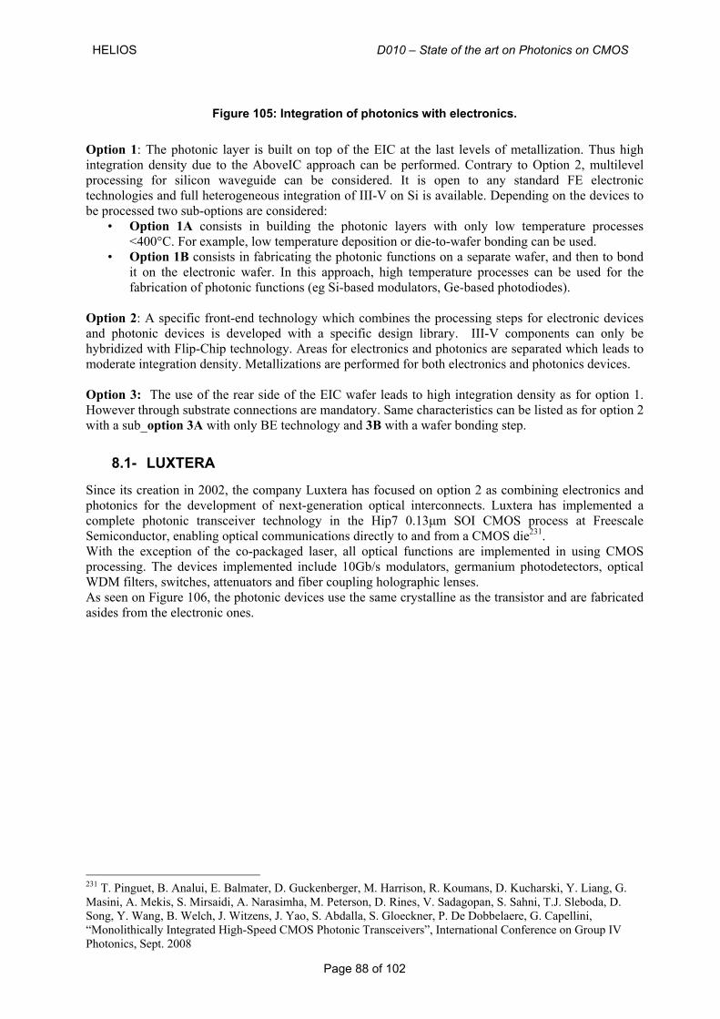
HELIOS D010 – State of the art on Photonics on CMOS
Page 88 of 102
Figure 105: Integration of photonics with electronics.
Option 1: The photonic layer is built on top of the EIC at the last levels of metallization. Thus high integration density due to the AboveIC approach can be performed. Contrary to Option 2, multilevel processing for silicon waveguide can be considered. It is open to any standard FE electronic technologies and full heterogeneous integration of III-V on Si is available. Depending on the devices to be processed two sub-options are considered:
• Option 1A consists in building the photonic layers with only low temperature processes <400°C. For example, low temperature deposition or die-to-wafer bonding can be used.
• Option 1B consists in fabricating the photonic functions on a separate wafer, and then to bond it on the electronic wafer. In this approach, high temperature processes can be used for the fabrication of photonic functions (eg Si-based modulators, Ge-based photodiodes).
Option 2: A specific front-end technology which combines the processing steps for electronic devices and photonic devices is developed with a specific design library. III-V components can only be hybridized with Flip-Chip technology. Areas for electronics and photonics are separated which leads to moderate integration density. Metallizations are performed for both electronics and photonics devices. Option 3: The use of the rear side of the EIC wafer leads to high integration density as for option 1. However through substrate connections are mandatory. Same characteristics can be listed as for option 2 with a sub_option 3A with only BE technology and 3B with a wafer bonding step.
8.1- LUXTERA
Since its creation in 2002, the company Luxtera has focused on option 2 as combining electronics and photonics for the development of next-generation optical interconnects. Luxtera has implemented a complete photonic transceiver technology in the Hip7 0.13μm SOI CMOS process at Freescale Semiconductor, enabling optical communications directly to and from a CMOS die231. With the exception of the co-packaged laser, all optical functions are implemented in using CMOS processing. The devices implemented include 10Gb/s modulators, germanium photodetectors, optical WDM filters, switches, attenuators and fiber coupling holographic lenses. As seen on Figure 106, the photonic devices use the same crystalline as the transistor and are fabricated asides from the electronic ones.
231 T. Pinguet, B. Analui, E. Balmater, D. Guckenberger, M. Harrison, R. Koumans, D. Kucharski, Y. Liang, G. Masini, A. Mekis, S. Mirsaidi, A. Narasimha, M. Peterson, D. Rines, V. Sadagopan, S. Sahni, T.J. Sleboda, D. Song, Y. Wang, B. Welch, J. Witzens, J. Yao, S. Abdalla, S. Gloeckner, P. De Dobbelaere, G. Capellini, “Monolithically Integrated High-Speed CMOS Photonic Transceivers”, International Conference on Group IV Photonics, Sept. 2008
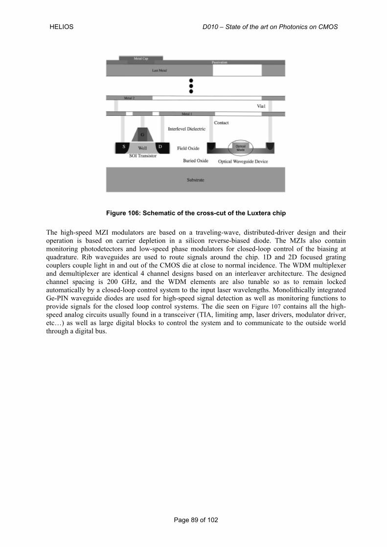
HELIOS D010 – State of the art on Photonics on CMOS
Page 89 of 102
Figure 106: Schematic of the cross-cut of the Luxtera chip
The high-speed MZI modulators are based on a traveling-wave, distributed-driver design and their operation is based on carrier depletion in a silicon reverse-biased diode. The MZIs also contain monitoring photodetectors and low-speed phase modulators for closed-loop control of the biasing at quadrature. Rib waveguides are used to route signals around the chip. 1D and 2D focused grating couplers couple light in and out of the CMOS die at close to normal incidence. The WDM multiplexer and demultiplexer are identical 4 channel designs based on an interleaver architecture. The designed channel spacing is 200 GHz, and the WDM elements are also tunable so as to remain locked automatically by a closed-loop control system to the input laser wavelengths. Monolithically integrated Ge-PIN waveguide diodes are used for high-speed signal detection as well as monitoring functions to provide signals for the closed loop control systems. The die seen on Figure 107 contains all the high-speed analog circuits usually found in a transceiver (TIA, limiting amp, laser drivers, modulator driver, etc…) as well as large digital blocks to control the system and to communicate to the outside world through a digital bus.
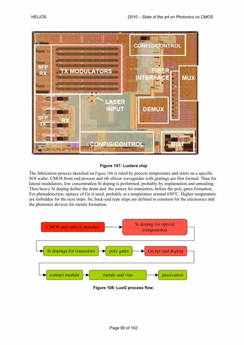
HELIOS D010 – State of the art on Photonics on CMOS
Page 90 of 102
Figure 107: Luxtera chip
The fabrication process sketched on Figure 108 is ruled by process temperature and starts on a specific SOI wafer. CMOS front end process and rib silicon waveguides with gratings are first formed. Then for lateral modulators, low concentration Si doping is performed, probably by implantation and annealing. Then heavy Si doping define the drain and the source for transistors, before the poly gates formation. For photodetection, epitaxy of Ge is used, probably at a temperature around 650°C. Higher temperature are forbidden for the next steps. So, back-end type steps are defined in common for the electronics and the photonics devices for metals formation.
Figure 108: LuxG process flow.
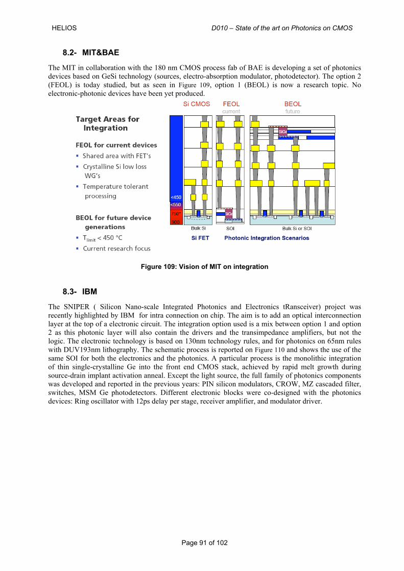
HELIOS D010 – State of the art on Photonics on CMOS
Page 91 of 102
8.2- MIT&BAE
The MIT in collaboration with the 180 nm CMOS process fab of BAE is developing a set of photonics devices based on GeSi technology (sources, electro-absorption modulator, photodetector). The option 2 (FEOL) is today studied, but as seen in Figure 109, option 1 (BEOL) is now a research topic. No electronic-photonic devices have been yet produced.
Figure 109: Vision of MIT on integration
8.3- IBM
The SNIPER ( Silicon Nano-scale Integrated Photonics and Electronics tRansceiver) project was recently highlighted by IBM for intra connection on chip. The aim is to add an optical interconnection layer at the top of a electronic circuit. The integration option used is a mix between option 1 and option 2 as this photonic layer will also contain the drivers and the transimpedance amplifiers, but not the logic. The electronic technology is based on 130nm technology rules, and for photonics on 65nm rules with DUV193nm lithography. The schematic process is reported on Figure 110 and shows the use of the same SOI for both the electronics and the photonics. A particular process is the monolithic integration of thin single-crystalline Ge into the front end CMOS stack, achieved by rapid melt growth during source-drain implant activation anneal. Except the light source, the full family of photonics components was developed and reported in the previous years: PIN silicon modulators, CROW, MZ cascaded filter, switches, MSM Ge photodetectors. Different electronic blocks were co-designed with the photonics devices: Ring oscillator with 12ps delay per stage, receiver amplifier, and modulator driver.
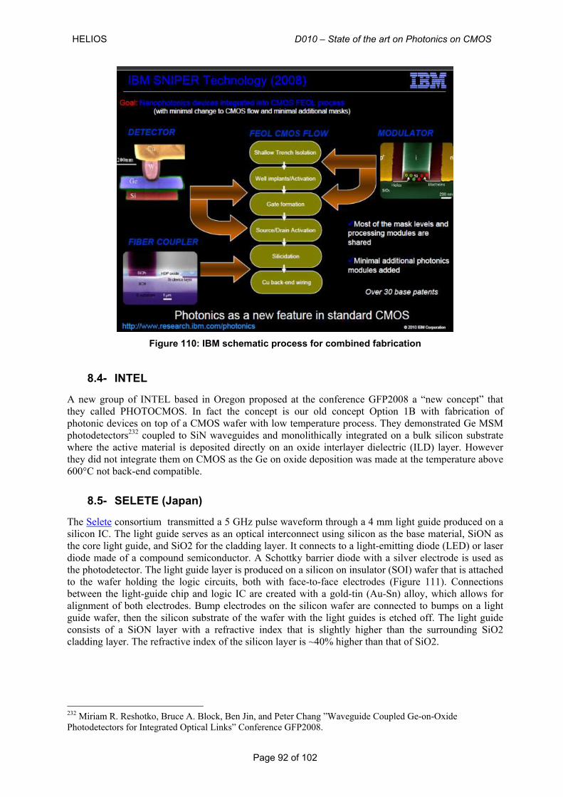
HELIOS D010 – State of the art on Photonics on CMOS
Page 92 of 102
Figure 110: IBM schematic process for combined fabrication
8.4- INTEL
A new group of INTEL based in Oregon proposed at the conference GFP2008 a “new concept” that they called PHOTOCMOS. In fact the concept is our old concept Option 1B with fabrication of photonic devices on top of a CMOS wafer with low temperature process. They demonstrated Ge MSM photodetectors232 coupled to SiN waveguides and monolithically integrated on a bulk silicon substrate where the active material is deposited directly on an oxide interlayer dielectric (ILD) layer. However they did not integrate them on CMOS as the Ge on oxide deposition was made at the temperature above 600°C not back-end compatible.
8.5- SELETE (Japan)
The Selete consortium transmitted a 5 GHz pulse waveform through a 4 mm light guide produced on a silicon IC. The light guide serves as an optical interconnect using silicon as the base material, SiON as the core light guide, and SiO2 for the cladding layer. It connects to a light-emitting diode (LED) or laser diode made of a compound semiconductor. A Schottky barrier diode with a silver electrode is used as the photodetector. The light guide layer is produced on a silicon on insulator (SOI) wafer that is attached to the wafer holding the logic circuits, both with face-to-face electrodes (Figure 111). Connections between the light-guide chip and logic IC are created with a gold-tin (Au-Sn) alloy, which allows for alignment of both electrodes. Bump electrodes on the silicon wafer are connected to bumps on a light guide wafer, then the silicon substrate of the wafer with the light guides is etched off. The light guide consists of a SiON layer with a refractive index that is slightly higher than the surrounding SiO2 cladding layer. The refractive index of the silicon layer is ~40% higher than that of SiO2.
232 Miriam R. Reshotko, Bruce A. Block, Ben Jin, and Peter Chang ”Waveguide Coupled Ge-on-Oxide Photodetectors for Integrated Optical Links” Conference GFP2008.
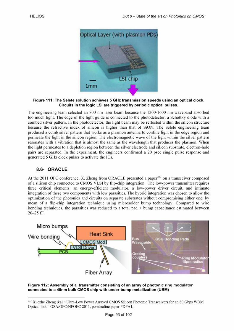
HELIOS D010 – State of the art on Photonics on CMOS
Page 93 of 102
Figure 111: The Selete solution achieves 5 GHz transmission speeds using an optical clock.
Circuits in the logic LSI are triggered by periodic optical pulses. The engineering team selected an 800 nm laser beam because the 1300-1600 nm waveband absorbed too much light. The edge of the light guide is connected to the photodetector, a Schottky diode with a combed silver pattern. In the photodetector, the light beam may be reflected within the silicon structure because the refractive index of silicon is higher than that of SiON. The Selete engineering team produced a comb silver pattern that works as a plasmon antenna to confine light in the edge region and permeate the light in the silicon region. The electromagnetic wave of the light within the silver pattern resonates with a vibration that is almost the same as the wavelength that produces the plasmon. When the light permeates to a depletion region between the silver electrode and silicon substrate, electron-hole pairs are separated. In the experiment, the engineers confirmed a 20 psec single pulse response and generated 5 GHz clock pulses to activate the ICs.
8.6- ORACLE
At the 2011 OFC conference, X. Zheng from ORACLE presented a paper233 on a transceiver composed of a silicon chip connected to CMOS VLSI by flip-chip integration. The low-power transmitter requires three critical elements: an energy-efficient modulator, a low-power driver circuit, and intimate integration of these two components with low parasitics. The hybrid integration was chosen to allow the optimization of the photonics and circuits on separate substrates without compromising either one, by mean of a flip-chip integration technique using microsolder bump technology. Compared to wire bonding techniques, the parasitics was reduced to a total pad + bump capacitance estimated between 20–25 fF.
Figure 112: Assembly of a transmitter consisting of an array of photonic ring modulator connected to a 40nm bulk CMOS chip with under-bump metallization (UBM)
233 Xuezhe Zheng &al “ Ultra-Low Power Arrayed CMOS Silicon Photonic Transceivers for an 80 Gbps WDM Optical link” OSA/OFC/NFOEC 2011, postdealine paper PDPA1,
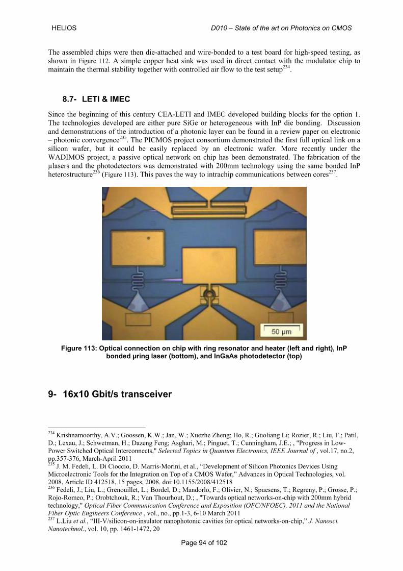
HELIOS D010 – State of the art on Photonics on CMOS
Page 94 of 102
The assembled chips were then die-attached and wire-bonded to a test board for high-speed testing, as shown in Figure 112. A simple copper heat sink was used in direct contact with the modulator chip to maintain the thermal stability together with controlled air flow to the test setup234.
8.7- LETI & IMEC
Since the beginning of this century CEA-LETI and IMEC developed building blocks for the option 1. The technologies developed are either pure SiGe or heterogeneous with InP die bonding. Discussion and demonstrations of the introduction of a photonic layer can be found in a review paper on electronic – photonic convergence235. The PICMOS project consortium demonstrated the first full optical link on a silicon wafer, but it could be easily replaced by an electronic wafer. More recently under the WADIMOS project, a passive optical network on chip has been demonstrated. The fabrication of the µlasers and the photodetectors was demonstrated with 200mm technology using the same bonded InP heterostructure236 (Figure 113). This paves the way to intrachip communications between cores237.
Figure 113: Optical connection on chip with ring resonator and heater (left and right), InP
bonded µring laser (bottom), and InGaAs photodetector (top)
9- 16x10 Gbit/s transceiver
234 Krishnamoorthy, A.V.; Goossen, K.W.; Jan, W.; Xuezhe Zheng; Ho, R.; Guoliang Li; Rozier, R.; Liu, F.; Patil, D.; Lexau, J.; Schwetman, H.; Dazeng Feng; Asghari, M.; Pinguet, T.; Cunningham, J.E.; , "Progress in Low-Power Switched Optical Interconnects," Selected Topics in Quantum Electronics, IEEE Journal of , vol.17, no.2, pp.357-376, March-April 2011 235 J. M. Fedeli, L. Di Cioccio, D. Marris-Morini, et al., “Development of Silicon Photonics Devices Using Microelectronic Tools for the Integration on Top of a CMOS Wafer,” Advances in Optical Technologies, vol. 2008, Article ID 412518, 15 pages, 2008. doi:10.1155/2008/412518 236 Fedeli, J.; Liu, L.; Grenouillet, L.; Bordel, D.; Mandorlo, F.; Olivier, N.; Spuesens, T.; Regreny, P.; Grosse, P.; Rojo-Romeo, P.; Orobtchouk, R.; Van Thourhout, D.; , "Towards optical networks-on-chip with 200mm hybrid technology," Optical Fiber Communication Conference and Exposition (OFC/NFOEC), 2011 and the National Fiber Optic Engineers Conference , vol., no., pp.1-3, 6-10 March 2011 237 L.Liu et al., “III-V/silicon-on-insulator nanophotonic cavities for optical networks-on-chip,” J. Nanosci. Nanotechnol., vol. 10, pp. 1461-1472, 20
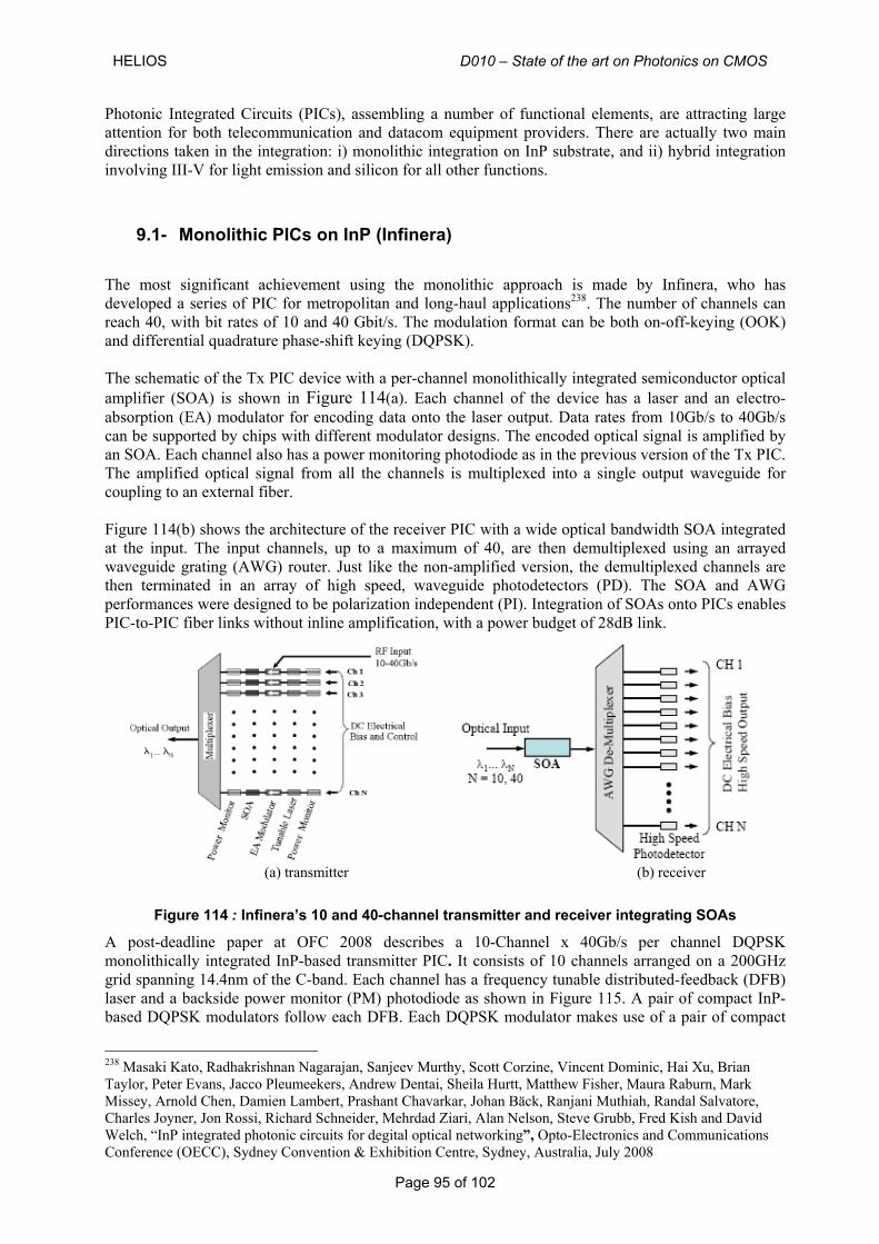
HELIOS D010 – State of the art on Photonics on CMOS
Page 95 of 102
Photonic Integrated Circuits (PICs), assembling a number of functional elements, are attracting large attention for both telecommunication and datacom equipment providers. There are actually two main directions taken in the integration: i) monolithic integration on InP substrate, and ii) hybrid integration involving III-V for light emission and silicon for all other functions.
9.1- Monolithic PICs on InP (Infinera)
The most significant achievement using the monolithic approach is made by Infinera, who has developed a series of PIC for metropolitan and long-haul applications238. The number of channels can reach 40, with bit rates of 10 and 40 Gbit/s. The modulation format can be both on-off-keying (OOK) and differential quadrature phase-shift keying (DQPSK). The schematic of the Tx PIC device with a per-channel monolithically integrated semiconductor optical amplifier (SOA) is shown in Figure 114(a). Each channel of the device has a laser and an electro-absorption (EA) modulator for encoding data onto the laser output. Data rates from 10Gb/s to 40Gb/s can be supported by chips with different modulator designs. The encoded optical signal is amplified by an SOA. Each channel also has a power monitoring photodiode as in the previous version of the Tx PIC. The amplified optical signal from all the channels is multiplexed into a single output waveguide for coupling to an external fiber. Figure 114(b) shows the architecture of the receiver PIC with a wide optical bandwidth SOA integrated at the input. The input channels, up to a maximum of 40, are then demultiplexed using an arrayed waveguide grating (AWG) router. Just like the non-amplified version, the demultiplexed channels are then terminated in an array of high speed, waveguide photodetectors (PD). The SOA and AWG performances were designed to be polarization independent (PI). Integration of SOAs onto PICs enables PIC-to-PIC fiber links without inline amplification, with a power budget of 28dB link.
(a) transmitter (b) receiver
Figure 114 : Infinera’s 10 and 40-channel transmitter and receiver integrating SOAs
A post-deadline paper at OFC 2008 describes a 10-Channel x 40Gb/s per channel DQPSK monolithically integrated InP-based transmitter PIC. It consists of 10 channels arranged on a 200GHz grid spanning 14.4nm of the C-band. Each channel has a frequency tunable distributed-feedback (DFB) laser and a backside power monitor (PM) photodiode as shown in Figure 115. A pair of compact InP-based DQPSK modulators follow each DFB. Each DQPSK modulator makes use of a pair of compact
238 Masaki Kato, Radhakrishnan Nagarajan, Sanjeev Murthy, Scott Corzine, Vincent Dominic, Hai Xu, Brian Taylor, Peter Evans, Jacco Pleumeekers, Andrew Dentai, Sheila Hurtt, Matthew Fisher, Maura Raburn, Mark Missey, Arnold Chen, Damien Lambert, Prashant Chavarkar, Johan Bäck, Ranjani Muthiah, Randal Salvatore, Charles Joyner, Jon Rossi, Richard Schneider, Mehrdad Ziari, Alan Nelson, Steve Grubb, Fred Kish and David Welch, “InP integrated photonic circuits for degital optical networking”, Opto-Electronics and Communications Conference (OECC), Sydney Convention & Exhibition Centre, Sydney, Australia, July 2008
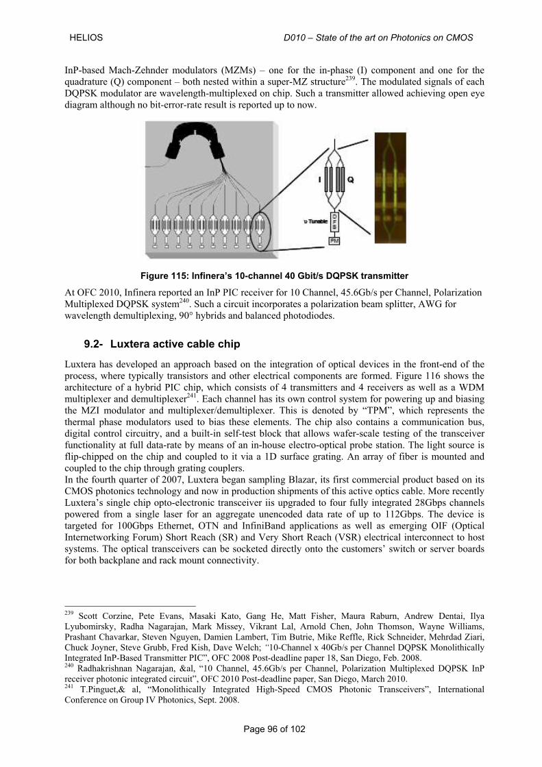
HELIOS D010 – State of the art on Photonics on CMOS
Page 96 of 102
InP-based Mach-Zehnder modulators (MZMs) – one for the in-phase (I) component and one for the quadrature (Q) component – both nested within a super-MZ structure239. The modulated signals of each DQPSK modulator are wavelength-multiplexed on chip. Such a transmitter allowed achieving open eye diagram although no bit-error-rate result is reported up to now.
Figure 115: Infinera’s 10-channel 40 Gbit/s DQPSK transmitter
At OFC 2010, Infinera reported an InP PIC receiver for 10 Channel, 45.6Gb/s per Channel, Polarization Multiplexed DQPSK system240. Such a circuit incorporates a polarization beam splitter, AWG for wavelength demultiplexing, 90° hybrids and balanced photodiodes.
9.2- Luxtera active cable chip
Luxtera has developed an approach based on the integration of optical devices in the front-end of the process, where typically transistors and other electrical components are formed. Figure 116 shows the architecture of a hybrid PIC chip, which consists of 4 transmitters and 4 receivers as well as a WDM multiplexer and demultiplexer241. Each channel has its own control system for powering up and biasing the MZI modulator and multiplexer/demultiplexer. This is denoted by “TPM”, which represents the thermal phase modulators used to bias these elements. The chip also contains a communication bus, digital control circuitry, and a built-in self-test block that allows wafer-scale testing of the transceiver functionality at full data-rate by means of an in-house electro-optical probe station. The light source is flip-chipped on the chip and coupled to it via a 1D surface grating. An array of fiber is mounted and coupled to the chip through grating couplers. In the fourth quarter of 2007, Luxtera began sampling Blazar, its first commercial product based on its CMOS photonics technology and now in production shipments of this active optics cable. More recently Luxtera’s single chip opto-electronic transceiver iis upgraded to four fully integrated 28Gbps channels powered from a single laser for an aggregate unencoded data rate of up to 112Gbps. The device is targeted for 100Gbps Ethernet, OTN and InfiniBand applications as well as emerging OIF (Optical Internetworking Forum) Short Reach (SR) and Very Short Reach (VSR) electrical interconnect to host systems. The optical transceivers can be socketed directly onto the customers’ switch or server boards for both backplane and rack mount connectivity.
239 Scott Corzine, Pete Evans, Masaki Kato, Gang He, Matt Fisher, Maura Raburn, Andrew Dentai, Ilya Lyubomirsky, Radha Nagarajan, Mark Missey, Vikrant Lal, Arnold Chen, John Thomson, Wayne Williams, Prashant Chavarkar, Steven Nguyen, Damien Lambert, Tim Butrie, Mike Reffle, Rick Schneider, Mehrdad Ziari, Chuck Joyner, Steve Grubb, Fred Kish, Dave Welch; “10-Channel x 40Gb/s per Channel DQPSK Monolithically Integrated InP-Based Transmitter PIC”, OFC 2008 Post-deadline paper 18, San Diego, Feb. 2008. 240 Radhakrishnan Nagarajan, &al, “10 Channel, 45.6Gb/s per Channel, Polarization Multiplexed DQPSK InP receiver photonic integrated circuit”, OFC 2010 Post-deadline paper, San Diego, March 2010. 241 T.Pinguet,& al, “Monolithically Integrated High-Speed CMOS Photonic Transceivers”, International Conference on Group IV Photonics, Sept. 2008.
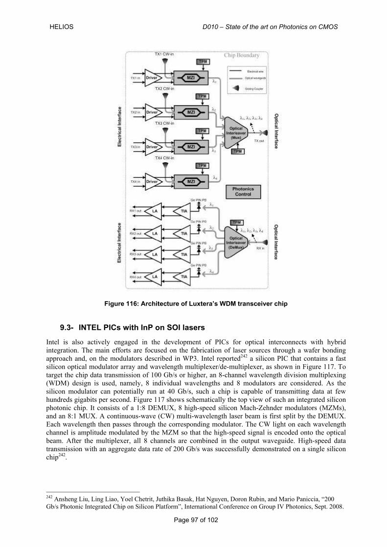
HELIOS D010 – State of the art on Photonics on CMOS
Page 97 of 102
Figure 116: Architecture of Luxtera’s WDM transceiver chip
9.3- INTEL PICs with InP on SOI lasers
Intel is also actively engaged in the development of PICs for optical interconnects with hybrid integration. The main efforts are focused on the fabrication of laser sources through a wafer bonding approach and, on the modulators described in WP3. Intel reported242 a silicon PIC that contains a fast silicon optical modulator array and wavelength multiplexer/de-multiplexer, as shown in Figure 117. To target the chip data transmission of 100 Gb/s or higher, an 8-channel wavelength division multiplexing (WDM) design is used, namely, 8 individual wavelengths and 8 modulators are considered. As the silicon modulator can potentially run at 40 Gb/s, such a chip is capable of transmitting data at few hundreds gigabits per second. Figure 117 shows schematically the top view of such an integrated silicon photonic chip. It consists of a 1:8 DEMUX, 8 high-speed silicon Mach-Zehnder modulators (MZMs), and an 8:1 MUX. A continuous-wave (CW) multi-wavelength laser beam is first split by the DEMUX. Each wavelength then passes through the corresponding modulator. The CW light on each wavelength channel is amplitude modulated by the MZM so that the high-speed signal is encoded onto the optical beam. After the multiplexer, all 8 channels are combined in the output waveguide. High-speed data transmission with an aggregate data rate of 200 Gb/s was successfully demonstrated on a single silicon chip242.
242 Ansheng Liu, Ling Liao, Yoel Chetrit, Juthika Basak, Hat Nguyen, Doron Rubin, and Mario Paniccia, “200 Gb/s Photonic Integrated Chip on Silicon Platform”, International Conference on Group IV Photonics, Sept. 2008.
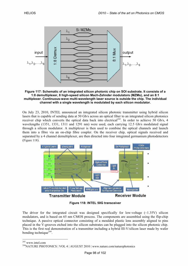
HELIOS D010 – State of the art on Photonics on CMOS
Page 98 of 102
Figure 117: Schematic of an integrated silicon photonic chip on SOI substrate. It consists of a
1:8 demultiplexer, 8 high-speed silicon Mach-Zehnder modulators (MZMs), and an 8:1 multiplexer. Continuous-wave multi-wavelength laser source is outside the chip. The individual
channel with a single wavelength is modulated by each silicon modulator.
On July 23, 2010, INTEL announced an integrated silicon photonic transmitter using hybrid silicon lasers that is capable of sending data at 50 Gb/s across an optical fiber to an integrated silicon photonics receiver chip which converts the optical data back into electrical243. In order to achieve 50 Gb/s, 4 wavelengths (1351, 1331, 1311 and 1291 nm) were used, each carrying 12.5 Gb/s modulated signal through a silicon modulator. A multiplexer is then used to combine the optical channels and launch them into a fibre via an on-chip fibre coupler. On the receiver chip, optical signals received and separated by a 4 channel demultiplexer, are then directed into four integrated germanium photodetectors (Figure 118).
Figure 118: INTEL 50G transceiver
The driver for the integrated circuit was designed specifically for low-voltage (~1.35V) silicon modulators, and is based on 65 nm CMOS process. The components are assembled using the flip-chip technique. A passive optical connector consisting of a moulded plastic lens assembly aligned to pins placed in the V-grooves etched into the silicon substrates can be plugged into the silicon photonic chip. This is the first real demonstration of a transmitter including a hybrid III-V/silicon laser made by wafer bonding technique244.
243 www.intel.com 244NATURE PHOTONICS | VOL 4 | AUGUST 2010 | www.nature.com/naturephotonics
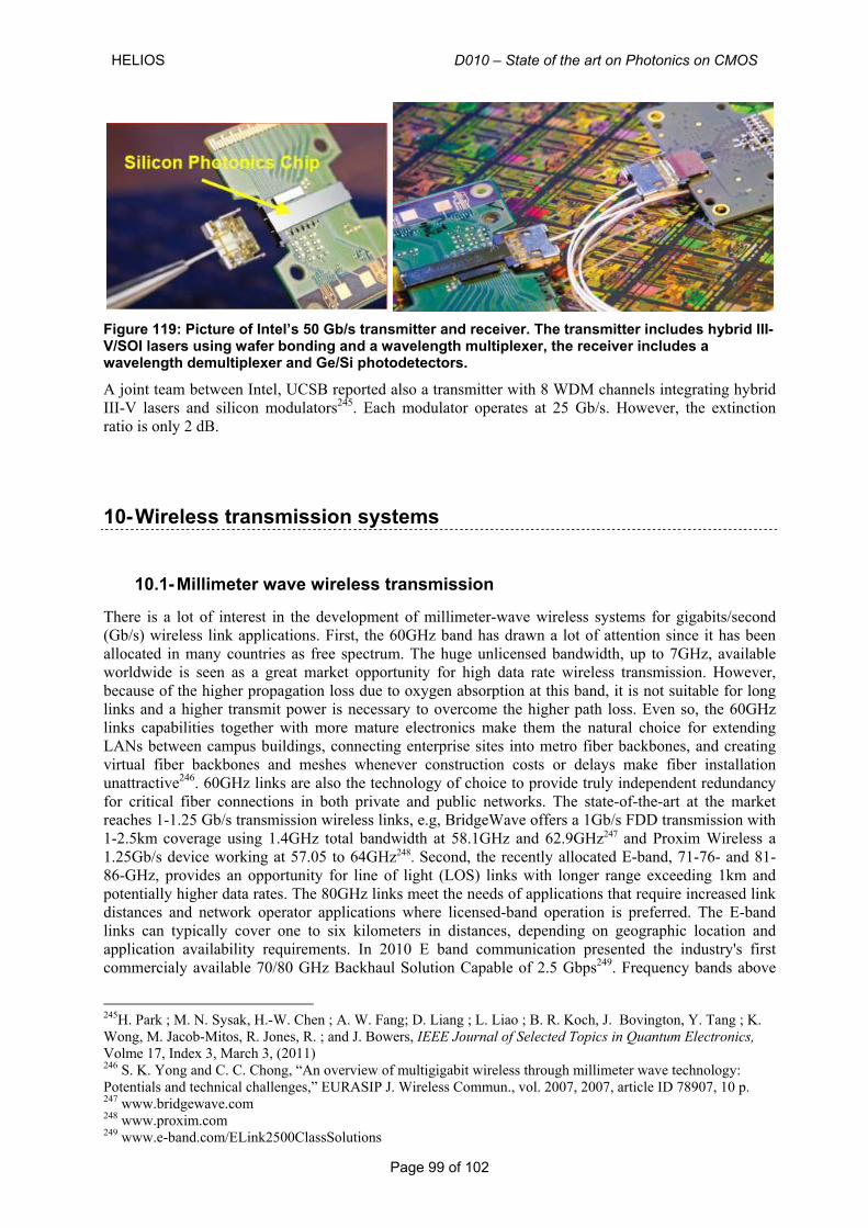
HELIOS D010 – State of the art on Photonics on CMOS
Page 99 of 102
Figure 119: Picture of Intel’s 50 Gb/s transmitter and receiver. The transmitter includes hybrid III-V/SOI lasers using wafer bonding and a wavelength multiplexer, the receiver includes a wavelength demultiplexer and Ge/Si photodetectors.
A joint team between Intel, UCSB reported also a transmitter with 8 WDM channels integrating hybrid III-V lasers and silicon modulators245. Each modulator operates at 25 Gb/s. However, the extinction ratio is only 2 dB.
10- Wireless transmission systems
10.1- Millimeter wave wireless transmission
There is a lot of interest in the development of millimeter-wave wireless systems for gigabits/second (Gb/s) wireless link applications. First, the 60GHz band has drawn a lot of attention since it has been allocated in many countries as free spectrum. The huge unlicensed bandwidth, up to 7GHz, available worldwide is seen as a great market opportunity for high data rate wireless transmission. However, because of the higher propagation loss due to oxygen absorption at this band, it is not suitable for long links and a higher transmit power is necessary to overcome the higher path loss. Even so, the 60GHz links capabilities together with more mature electronics make them the natural choice for extending LANs between campus buildings, connecting enterprise sites into metro fiber backbones, and creating virtual fiber backbones and meshes whenever construction costs or delays make fiber installation unattractive246. 60GHz links are also the technology of choice to provide truly independent redundancy for critical fiber connections in both private and public networks. The state-of-the-art at the market reaches 1-1.25 Gb/s transmission wireless links, e.g, BridgeWave offers a 1Gb/s FDD transmission with 1-2.5km coverage using 1.4GHz total bandwidth at 58.1GHz and 62.9GHz247 and Proxim Wireless a 1.25Gb/s device working at 57.05 to 64GHz248. Second, the recently allocated E-band, 71-76- and 81-86-GHz, provides an opportunity for line of light (LOS) links with longer range exceeding 1km and potentially higher data rates. The 80GHz links meet the needs of applications that require increased link distances and network operator applications where licensed-band operation is preferred. The E-band links can typically cover one to six kilometers in distances, depending on geographic location and application availability requirements. In 2010 E band communication presented the industry's first commercialy available 70/80 GHz Backhaul Solution Capable of 2.5 Gbps249. Frequency bands above
245H. Park ; M. N. Sysak, H.-W. Chen ; A. W. Fang; D. Liang ; L. Liao ; B. R. Koch, J. Bovington, Y. Tang ; K. Wong, M. Jacob-Mitos, R. Jones, R. ; and J. Bowers, IEEE Journal of Selected Topics in Quantum Electronics, Volme 17, Index 3, March 3, (2011) 246 S. K. Yong and C. C. Chong, “An overview of multigigabit wireless through millimeter wave technology: Potentials and technical challenges,” EURASIP J. Wireless Commun., vol. 2007, 2007, article ID 78907, 10 p. 247 www.bridgewave.com 248 www.proxim.com 249 www.e-band.com/ELink2500ClassSolutions
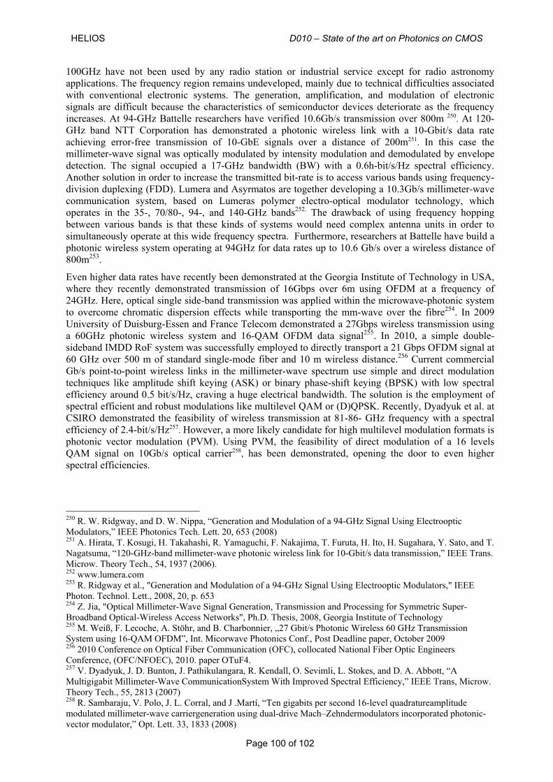
HELIOS D010 – State of the art on Photonics on CMOS
Page 100 of 102
100GHz have not been used by any radio station or industrial service except for radio astronomy applications. The frequency region remains undeveloped, mainly due to technical difficulties associated with conventional electronic systems. The generation, amplification, and modulation of electronic signals are difficult because the characteristics of semiconductor devices deteriorate as the frequency increases. At 94-GHz Battelle researchers have verified 10.6Gb/s transmission over 800m 250. At 120-GHz band NTT Corporation has demonstrated a photonic wireless link with a 10-Gbit/s data rate achieving error-free transmission of 10-GbE signals over a distance of 200m251. In this case the millimeter-wave signal was optically modulated by intensity modulation and demodulated by envelope detection. The signal occupied a 17-GHz bandwidth (BW) with a 0.6h-bit/s/Hz spectral efficiency. Another solution in order to increase the transmitted bit-rate is to access various bands using frequency-division duplexing (FDD). Lumera and Asyrmatos are together developing a 10.3Gb/s millimeter-wave communication system, based on Lumeras polymer electro-optical modulator technology, which operates in the 35-, 70/80-, 94-, and 140-GHz bands252. The drawback of using frequency hopping between various bands is that these kinds of systems would need complex antenna units in order to simultaneously operate at this wide frequency spectra. Furthermore, researchers at Battelle have build a photonic wireless system operating at 94GHz for data rates up to 10.6 Gb/s over a wireless distance of 800m253.
Even higher data rates have recently been demonstrated at the Georgia Institute of Technology in USA, where they recently demonstrated transmission of 16Gbps over 6m using OFDM at a frequency of 24GHz. Here, optical single side-band transmission was applied within the microwave-photonic system to overcome chromatic dispersion effects while transporting the mm-wave over the fibre254. In 2009 University of Duisburg-Essen and France Telecom demonstrated a 27Gbps wireless transmission using a 60GHz photonic wireless system and 16-QAM OFDM data signal255. In 2010, a simple double-sideband IMDD RoF system was successfully employed to directly transport a 21 Gbps OFDM signal at 60 GHz over 500 m of standard single-mode fiber and 10 m wireless distance.256 Current commercial Gb/s point-to-point wireless links in the millimeter-wave spectrum use simple and direct modulation techniques like amplitude shift keying (ASK) or binary phase-shift keying (BPSK) with low spectral efficiency around 0.5 bit/s/Hz, craving a huge electrical bandwidth. The solution is the employment of spectral efficient and robust modulations like multilevel QAM or (D)QPSK. Recently, Dyadyuk et al. at CSIRO demonstrated the feasibility of wireless transmission at 81-86- GHz frequency with a spectral efficiency of 2.4-bit/s/Hz257. However, a more likely candidate for high multilevel modulation formats is photonic vector modulation (PVM). Using PVM, the feasibility of direct modulation of a 16 levels QAM signal on 10Gb/s optical carrier258, has been demonstrated, opening the door to even higher spectral efficiencies.
250 R. W. Ridgway, and D. W. Nippa, “Generation and Modulation of a 94-GHz Signal Using Electrooptic Modulators,” IEEE Photonics Tech. Lett. 20, 653 (2008) 251 A. Hirata, T. Kosugi, H. Takahashi, R. Yamaguchi, F. Nakajima, T. Furuta, H. Ito, H. Sugahara, Y. Sato, and T. Nagatsuma, “120-GHz-band millimeter-wave photonic wireless link for 10-Gbit/s data transmission,” IEEE Trans. Microw. Theory Tech., 54, 1937 (2006). 252 www.lumera.com 253 R. Ridgway et al., "Generation and Modulation of a 94-GHz Signal Using Electrooptic Modulators," IEEE Photon. Technol. Lett., 2008, 20, p. 653 254 Z. Jia, "Optical Millimeter-Wave Signal Generation, Transmission and Processing for Symmetric Super-Broadband Optical-Wireless Access Networks", Ph.D. Thesis, 2008, Georgia Institute of Technology 255 M. Weiß, F. Lecoche, A. Stöhr, and B. Charbonnier, „27 Gbit/s Photonic Wireless 60 GHz Transmission System using 16-QAM OFDM”, Int. Micorwave Photonics Conf., Post Deadline paper, October 2009 256 2010 Conference on Optical Fiber Communication (OFC), collocated National Fiber Optic Engineers Conference, (OFC/NFOEC), 2010. paper OTuF4. 257 V. Dyadyuk, J. D. Bunton, J. Pathikulangara, R. Kendall, O. Sevimli, L. Stokes, and D. A. Abbott, “A Multigigabit Millimeter-Wave CommunicationSystem With Improved Spectral Efficiency,” IEEE Trans, Microw. Theory Tech., 55, 2813 (2007) 258 R. Sambaraju, V. Polo, J. L. Corral, and J .Martí, “Ten gigabits per second 16-level quadratureamplitude modulated millimeter-wave carriergeneration using dual-drive Mach–Zehndermodulators incorporated photonic-vector modulator,” Opt. Lett. 33, 1833 (2008)
HELIOS D010 – State of the art on Photonics on CMOS
Page 101 of 102
10.2- Photonics wireless transmission systems
The duality provided by PVM relying on the efficient architecture design, simultaneous delivery of wired and wireless access services can be achieved in a single platform to serve both fixed and mobile users, makes the integration of fiber and radio communication, known as hybrid fiber-radio systems (HFR), possible. Furthermore, the technology is completely transparent; the same system technology can be used for any millimeter wave generation, modulation and demodulation including full scalability in bitrates. This transparency of the system creates a very flexible attraction for the market with no additional costs. The uses of photonic technologies in optical-wireless networks can significantly reduce the requirement of high-frequency electrical components for millimeter-wave signal processing. In the general PVM wireless scheme, no high level electrics, apart from the electrical tone oscillator, are needed in the generation process and, therefore, high data rates at high electrical frequencies can be obtained. In addition, the hardware requirements are reduced when compared to all-electronic architectures, so a highly compact low-cost architecture can be implemented.
The differential quadrature phase shift keying (DQPSK) modulation format is the PVM multilevel modulation format that has received most attention in optical communication 259. DQPSK transmitters are most conveniently implemented using two nested MZMs, operated as phase modulators, i.e. driven at 2-pi shift, an optical 90 degree-phase shifter in one of the paths, and a combiner to produce a single output signal. At the receiver, the DQPSK signal is first split into two equal parts, since DPSK cannot directly be received using square law detection, a Delay Interferometer (DI) is inserted in the optical path at the receiver to convert the differential phase modulation into intensity modulation. This photonic circuit is completely passive and the operation is carried out without the necessity of a Phase Lock Loop (PLL), which is used in non-integrated optics.
Optical heterodyning technology refers to the process where two optical lightwaves of different wavelengths beat each other at a photodetector to generate a millimeter-wave signal. This approach is only limited by the response of the photodetector. Since all the optical power contributes to the generated RF carrier, optical heterodyning can offer high RF power and high carrier-to-noise ratio. This technology can be achieved using three approaches;
o By two lasers that emit the light at wavelengths separated by the required millimeter-wave frequency;
o Using a modulated single mode laser;
o Using an optical frequency comb.
In general, the performance is limited by the phase noise and frequency stability of the lasers. To obtain a high-quality carrier, phase control mechanisms, such as optical injection locking and optical phase-locked loops, can be used. Even so, at an integrated level, the phase noise would be minimal while the signal propagates in the chip.
259 P. J. Winzer, and R Essiambre, “Advanced Optical Modulation Formats,” Proc. of the IEEE, 94, 952 (2006).

HELIOS D010 – State of the art on Photonics on CMOS
Page 102 of 102
11- List of abbreviations
AWG: arrayed waveguide grating BCB: Benzo-Cyclo-Butene BE: Back End CMOS: Complementary Metal Oxide Semiconductor DFB: Distributed Feed Back DBR: Distributed Bragg reflector DQPSK: Differential Quadrature Phase Shift Keying) DRC: Design Rule Checking DUV: Deep UV EDA: Electronic Design Automation EIC: electronic integrated circuit EQE: external quantum efficiency EL: Electro luminescence EO: electro-optic FE: Front-End FET: Field Effect transistors FK: Frantz Keldysh effect FP: Fabry-Perot IC: Integrated Circuit LED: Light Emitting Diode LVS: layout versus schematic MZI: Mach-Zehnder interferometer MZM: Mach-Zehnder modulator OPADM: Optical Packet Add/Drop Multiplexer PC: photonic crystal PIC: photonic integrated circuit PICMOS: photonic integrated circuit on CMOS PL: Photoluminescence PD: Photodetector PVM: Photonic vector modulation QAM: Quadrature amplitude modulation QCSE: quantum-confined Stark effect RAU: remote antenna unit RX: receiver SOI: silicon on insulator TE: Transverse Electric TIA: trans-impedance amplifier TM: Transverse Magnetic TRM: transmitter receive modules TX: transmitter VCSEL: vertical-cavity surface-emitting laser WDM: wavelength division multiplexing WOU: wireless optical unit