Embed Size (px)
Citation preview

CRYSTALS
OSCILLATORS
TCXOs
VCXOs
F I LTERS
FOX ELECTRONICS
F R E Q U E N C Y C O N T R O L P R O D U C T S
FOX
ELECTR
ON
ICS
VO
LUM
E TWEN
TY
www .foxon l ine .com
VOLUME TWENTY
FOX ELECTRONICS5570 Enterpr ise ParkwayFor t Myers , FL 33905Te l : 888-GET-2-FOXFax: 239-693-1554e-mai l : sa les@foxonl ine.com
Application Specific Crystals, Oscillators, TCXOs, VCXOs and OCXOs
Cost-Effective Development with Rapid Turnaround
Engineered Solutions from Minor Modifications to Full Custom
Dedicated Engineering Support Team for Your Application
Advanced Frequency Control Expertise from the World Leader
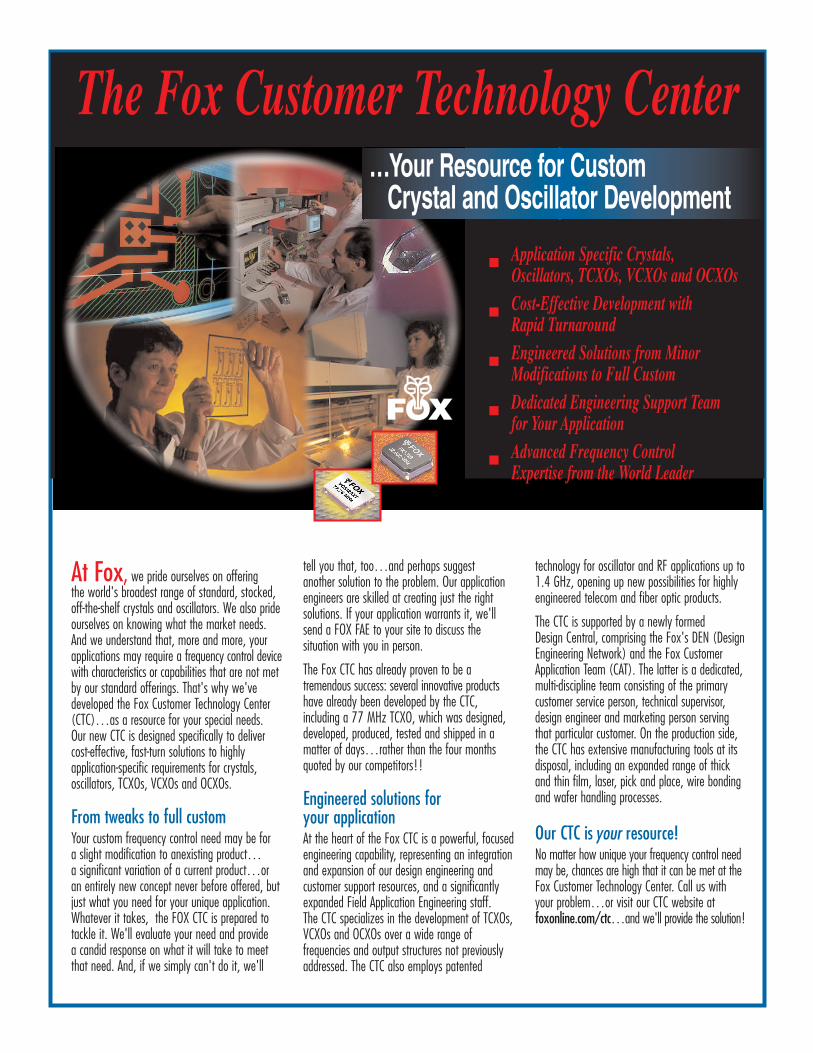
At Fox, we pride ourselves on offering the world's broadest range of standard, stocked, off-the-shelf crystals and oscillators. We also prideourselves on knowing what the market needs. And we understand that, more and more, yourapplications may require a frequency control devicewith characteristics or capabilities that are not metby our standard offerings. That's why we'vedeveloped the Fox Customer Technology Center(CTC)…as a resource for your special needs. Our new CTC is designed specifically to delivercost-effective, fast-turn solutions to highlyapplication-specific requirements for crystals,oscillators, TCXOs, VCXOs and OCXOs.
From tweaks to full customYour custom frequency control need may be for a slight modification to anexisting product…a significant variation of a current product…or an entirely new concept never before offered, butjust what you need for your unique application.Whatever it takes, the FOX CTC is prepared totackle it. We'll evaluate your need and provide a candid response on what it will take to meet that need. And, if we simply can't do it, we'll
tell you that, too…and perhaps suggest another solution to the problem. Our applicationengineers are skilled at creating just the rightsolutions. If your application warrants it, we'll send a FOX FAE to your site to discuss thesituation with you in person.
The Fox CTC has already proven to be atremendous success: several innovative productshave already been developed by the CTC, including a 77 MHz TCXO, which was designed,developed, produced, tested and shipped in amatter of days…rather than the four monthsquoted by our competitors!!
Engineered solutions for your applicationAt the heart of the Fox CTC is a powerful, focusedengineering capability, representing an integrationand expansion of our design engineering andcustomer support resources, and a significantlyexpanded Field Application Engineering staff. The CTC specializes in the development of TCXOs,VCXOs and OCXOs over a wide range offrequencies and output structures not previouslyaddressed. The CTC also employs patented
technology for oscillator and RF applications up to1.4 GHz, opening up new possibilities for highly engineered telecom and fiber optic products.
The CTC is supported by a newly formed Design Central, comprising the Fox's DEN (DesignEngineering Network) and the Fox CustomerApplication Team (CAT). The latter is a dedicated,multi-discipline team consisting of the primarycustomer service person, technical supervisor,design engineer and marketing person serving that particular customer. On the production side,the CTC has extensive manufacturing tools at itsdisposal, including an expanded range of thick and thin film, laser, pick and place, wire bondingand wafer handling processes.
Our CTC is your resource!No matter how unique your frequency control needmay be, chances are high that it can be met at theFox Customer Technology Center. Call us with your problem…or visit our CTC website atfoxonline.com/ctc…and we'll provide the solution!
The Fox Customer Technology Center…Your Resource for Custom
Crystal and Oscillator Development

1© 2002 FOX ELECTRONICS
FOXElectronics 5570 Enterprise Parkway Fort Myers, Florida 33905 USA +001(239)693-0099 FAX +001(239)693-1554 http://www.foxonline.com
Fox Electronics' mission is to provide a broad line of frequency control products to worldwide
electronics markets. Combining the disciplines of engineering, manufacturing, quality assurance,
operations, information systems and marketing, Fox strives to provide its customers with superior quality,
excellent service, leading edge products and knowledgeable application support.
MMMMMISSION ISSION ISSION ISSION ISSION SSSSSTTTTTAAAAATEMENTTEMENTTEMENTTEMENTTEMENT
Regular updates and New Product Announcements are made on our web site. Visit http://www.foxonline.com
Fox Electronics has a staff of application specialists ready to help you. Contact our hotline
tech_support @ foxonline.com

2 FOXElectronics 5570 Enterprise Parkway Fort Myers, Florida 33905 USA +001(239)693-0099 FAX +001(239)693-1554 http://www.foxonline.com© 2002 FOX ELECTRONICS
The FOX Mission .................................................................................................................................................. 1Contents .......................................................................................................................................................... 2 - 3
FOFOFOFOFOX SERX SERX SERX SERX SERVICESVICESVICESVICESVICESDistributor Briefing ................................................................................................................................................ 4Standard Microprocessor Crystals ........................................................................................................................ 5Standard Watch Crystals ....................................................................................................................................... 6Standard Oscillators .............................................................................................................................................. 7Standard TCXOs and VCXOs................................................................................................................................ 8JITO-2 & FASTFOX Product Lines ........................................................................................................................ 9
QQQQQUUUUUARARARARARTZ CRTZ CRTZ CRTZ CRTZ CRYYYYYSTSTSTSTSTALSALSALSALSALSQuartz Crystal Selection Guide ........................................................................................................................... 10FX325B......................................3.2 x 2.5mm Ceramic SMD ............................................................................. 11FX532 Series .............................5 x 3.2mm Ceramic SMD ................................................................................ 12FQA ...........................................6 x 3.5mm Ceramic Resin Sealed SMD ........................................................... 13FMB ...........................................6 x 3.5mm Ceramic Seam Sealed SMD .......................................................... 14FE..............................................7.5 x 5mm Ceramic Resin Sealed SMD ........................................................... 15FD..............................................7.5 x 5mm Ceramic Seam Sealed SMD .......................................................... 16FC..............................................11.8 x 5.5mm Ceramic Resin Sealed SMD ...................................................... 17FPX ...........................................12.9 x 5mm Plastic Encased SMD .................................................................. 18HC49SD .....................................13.2 x 4.8mm Resistance Weld SMD .............................................................. 19HC49S .......................................11.3 x 4.6mm Resistance Weld Thru-Hole ....................................................... 20HC80U .......................................6.9 x 8.1mm Resistance Weld Thru-Hole ......................................................... 21HC49U .......................................11 x 13.5mm Resistance Weld Thru-Hole ........................................................ 22
WWWWWAAAAATTTTTCH CRCH CRCH CRCH CRCH CRYYYYYSTSTSTSTSTALSALSALSALSALSFSX ...........................................7 x 1.5mm SMD Tuning Fork............................................................................ 23FSR327......................................8.7 x 3.7mm SMD Tuning Fork (Standard) ....................................................... 24NC Series ..................................1.5 x 5mm / 2 x 6mm / 3 x 8mm Thru-Hole Tuning Fork ................................... 25Crystal Part Description Guide ............................................................................................................................ 26SMD Crystals Tape And Reel Specifications ....................................................................................................... 27
CLCLCLCLCLOCK OSCILLAOCK OSCILLAOCK OSCILLAOCK OSCILLAOCK OSCILLATTTTTORSORSORSORSORSClock Oscillator Selection Guide ......................................................................................................................... 28Clock Oscillator General Characteristics ............................................................................................................. 29Just-In-Time Oscillators® (JITO®-2) .............................................................................................................. 30-35F510L Series..............................1.8V 5 x 3.2mm HCMOS Ceramic SMD with Standby ................................... 36F540L Series..............................2.5V 5 x 3.2mm HCMOS Ceramic SMD with Standby ................................... 37F530L Series..............................3.3V 5 x 3.2mm HCMOS Ceramic SMD with Standby ................................... 38F4200 Series..............................3.3V 6 x 3.5mm HCMOS Ceramic SMD with Standby ................................... 39F4500 Series..............................1.8V 7.5 x 5mm HCMOS SMD with Standby ................................................. 40F4400 Series..............................2.5V 7.5 x 5mm HCMOS SMD with Standby ................................................. 41F4100 Series..............................3.3V 7.5 x 5mm HCMOS SMD with Standby ............................................ 42-43F3345 Series..............................5.0V 7.5 x 5mm HCMOS/TTL SMD with Tri-State E/D ................................... 44F4600 Series..............................3.3V 7.5 x 5mm LV-PECL Ceramic SMD with Comp. Output ......................... 45KFO Series ................................3.3V/5.0V 12.8 x 9.8mm HCMOS/TTL Plastic SMD withTri-State E/D ........... 46FSO Series ................................3.3V/5.0V 14 x 9.8mm HCMOS/TTL Plastic SMD withTri-State E/D .............. 47
CATALOG CONTENTS

3© 2002 FOX ELECTRONICS
FOXElectronics 5570 Enterprise Parkway Fort Myers, Florida 33905 USA +001(239)693-0099 FAX +001(239)693-1554 http://www.foxonline.com
CRYSTALSW
ATCH CRYSTALSO
SCILLATORS
FILTERSO
CXOs
VCXO
s & TC
XOs
TECHNICAL
F5C-2E3 / H5C-2E3 ................... 3.3V 14-Pin/8-Pin DIP HCMOS/TTL Thru-Hole w/ Tri-State E/D ..................... 48F5C-2E / H5C-2E .......................5.0V 14-Pin/8-Pin DIP HCMOS Thru-Hole with Tri-State E/D .......................... 49F1100E ......................................5.0V 14-Pin DIP TTL Thru-Hole ...................................................................... 50F5L-4G.......................................5.0V 14-Pin DIP PECL Thru-Hole .................................................................. 51Oscillator Part Description Guide ........................................................................................................................ 52Oscillator Tape and Reel Specifications ............................................................................................................... 53
VVVVVOLOLOLOLOLTTTTTAAAAAGE CONTRGE CONTRGE CONTRGE CONTRGE CONTROLLED CROLLED CROLLED CROLLED CROLLED CRYYYYYSTSTSTSTSTAL OSCILLAAL OSCILLAAL OSCILLAAL OSCILLAAL OSCILLATTTTTORS (VORS (VORS (VORS (VORS (VCXCXCXCXCXO)O)O)O)O)VCXO, TCXO, and OCXO Selection Guide.......................................................................................................... 54VCS25AXT ................................3.3V 7.5 x 5mm HCMOS Ceramic SMD (Standard) ....................................... 55VCSAXT Series ......................... 3.3V 7.5 x 5mm HCMOS Ceramic SMD ........................................................ 56VCXO-D ..................................... 3.3V 14-Pin DIP HCMOS Thru-Hole .............................................................. 57VCXO-C ..................................... 5.0V 14-Pin DIP HCMOS Thru-Hole ............................................................... 58
TEMPERATEMPERATEMPERATEMPERATEMPERATURE COMPENSATURE COMPENSATURE COMPENSATURE COMPENSATURE COMPENSATED CRTED CRTED CRTED CRTED CRYYYYYSTSTSTSTSTAL OSCILLAAL OSCILLAAL OSCILLAAL OSCILLAAL OSCILLATTTTTORS (TORS (TORS (TORS (TORS (TCXCXCXCXCXO)O)O)O)O)FOX914 Series ...........................3.0V 5 x 3.2mm Clipped-Sine Ceramic SMD ................................................. 59FOX307H ...................................3.0V 7.5 x 5mm Clipped-Sine Ceramic SMD ................................................. 60FOX312BE .................................3.0V 7.5 x 5mm Clipped-Sine Ceramic SMD ................................................. 61FOX801BE .................................3.0V 11.4 x 9.6mm Clipped-Sine FR-4 SMD .................................................. 62FOX801 Series ...........................3.0V/5.0V 11.4 x 9.6mm Clipped-Sine FR-4 SMD ......................................... 63FOX781B ...................................5.0V 14-Pin DIP Clipped-Sine Thru-Hole ........................................................ 64FOX782......................................5.0V 14-Pin DIP HCMOS Thru-Hole ............................................................... 65
OOOOOVEN CONTRVEN CONTRVEN CONTRVEN CONTRVEN CONTROLLED CROLLED CROLLED CROLLED CROLLED CRYYYYYSTSTSTSTSTAL OSCILLAAL OSCILLAAL OSCILLAAL OSCILLAAL OSCILLATTTTTORS (OCXORS (OCXORS (OCXORS (OCXORS (OCXO)O)O)O)O)OCXO General Characteristics ........................................................................................................................... 66FTS501AH .................................3.3V/5.0V 14-Pin DIP HCMOS Thru-Hole ...................................................... 67VCXO and TCXO Part Description Guide ............................................................................................................ 68VCXO, TCXO, and OCXO Tape and Reel Specifications ..................................................................................... 69
CRCRCRCRCRYYYYYSTSTSTSTSTAL FILAL FILAL FILAL FILAL FILTERSTERSTERSTERSTERSMonolithic Crystal Filters ..................................................................................................................................... 70Standard Monolithic Crystal Filters ...................................................................................................................... 71Filters Part Description Guide ............................................................................................................................. 72
TECHNICAL DTECHNICAL DTECHNICAL DTECHNICAL DTECHNICAL DAAAAATTTTTAAAAAQuartz Crystal Theory of Operation ..................................................................................................................... 73Quartz Crystal Design Notes ....................................................................................................................... 74 - 75Oscillator Theory of Operation ...................................................................................................................... 76 - 78Frequently Asked Questions ........................................................................................................................ 79 - 80

4 FOXElectronics 5570 Enterprise Parkway Fort Myers, Florida 33905 USA +001(239)693-0099 FAX +001(239)693-1554 http://www.foxonline.com© 2002 FOX ELECTRONICS
DISTRIBUTOR BRIEFINGThe Fox Distribution Program includes all of the Fox Part Numbers identified as DISTRIBUTOR STOCKINGSTANDARDS plus all of our JITO-2 product line. Fox franchised distributors maintain inventory of theSTANDARDS to assure a constant supply to customers who design these items into their products. Of course,JITO-2 products are not maintained in inventory as they are 'built to order and schedule' for JIT delivery.
This STANDARDS PROGRAM is formalized in our distributor relationship and in our Contract Manufacturingrelationships, providing maximum global flexibility to our OEM customers. Design engineers can be confidentthat a STANDARD oscillator or crystal will be available for future manufacturing needs. A check with the Foxwebsite will reveal current address and phone number information for all of the authorized distributors in yourarea. The feature "StockCheck" on Fox's home page (www.foxonline.com) may be used to confirmdistributor inventory. Fox global distributors may have regional marketing centers in certain areas of the world,easily located through the distributors' website.
www.avnet.com
www.jacoelectronics.com
www.capsco.com
www.jandevices.com
www.dove-electronic.com
www.mouser.com
www.futureelectronics.com
www.progressiveimage.com
www.reptron.com
www.e-sonic.com
Global Distribution
North American Distribution
European DistributionEurosource
www.eurosource.co.ukMEV Elektronik
www.mev-elektronik.com
Singapore DistributionSeamax
Australian DistributionClarke & Severnwww.clarke.com.au

5© 2002 FOX ELECTRONICS
FOXElectronics 5570 Enterprise Parkway Fort Myers, Florida 33905 USA +001(239)693-0099 FAX +001(239)693-1554 http://www.foxonline.com
STANDARD
• Inventory Support
• Standard Packages
• Lowest Pricing
• Fox Quality
• Technical Support
CRYSTALS
ESR Ω
------------
200200200150150150150150150150---------------80808080---80---60606060---60606060604040---4040
---40---40303030303030---------------------
FPX------------FPX036SFPX0368SFPX0368-20FPX040AFPX040---------FPX049FPX049-20---------------FPX073FPX073-20FPX080FPX080-20---FPX081-20------FPX098-20FPX100FPX100-20---FPX111-20FPX115-20FPX120FPX120-20FPX128-20FPX143-20FPX147-20---FPX160FPX160-20---FPX184-20---FPX196-20FPX200FPX200-20FPX221-20FPX240F-20FPX245F-20FPX250F-20---FPX320-20 *FPX480-20 *FPX500-20 *---FPX600-20 *FPX640-20 *
CL
13pF20pF20pF32pF18pF
SERIES20pF
SERIES20pF20pF12pF20pF
SERIES20pF20pF
SERIES20pF30pF20pF
SERIES20pF
SERIES20pF
SERIES20pF
SERIESSERIES
20pFSERIES
20pFSERIES
20pF20pF
SERIES20pF20pF20pF20pF20pF
SERIES20pF
SERIES20pF
SERIES20pF
SERIES20pF20pF20pF20pF20pF20pF20pF20pF20pF18pF20pF20pF
FREQ (MHz)1.8432002.0000002.0971522.4576003.5795453.6864003.6864004.0000004.0000004.0960004.1943044.4336194.9152004.9152005.0000006.0000006.0000006.1440006.1440007.3728007.3728008.0000008.0000008.1920008.1920009.2160009.830400
9.83040010.000000
10.00000011.00000011.00000011.05920012.00000012.00000012.28800014.31818014.74560015.00000016.00000016.00000018.43200018.43200019.66080019.66080020.00000020.00000022.11840024.00000024.57600025.00000027.00000032.00000048.00000050.00000056.44800060.00000064.000000
HC49U
FOX018SFOX020SFOX021SFOX024SFOX036SFOX0368SFOX0368-20FOX040AFOX040FOX0496-20FOX041FOX0443FOX049FOX049-20FOX05AFOX060FOX060-20FOX061FOX061-20FOX073FOX073-20FOX080FOX080-20FOX081FOX081-20FOX092FOX098FOX098-20FOX100FOX100-20FOX111FOX111-20FOX115-20FOX120FOX120-20FOX128-20FOX143-20FOX147-20---FOX160FOX160-20FOX184FOX184-20FOX196FOX196-20FOX200FOX200-20FOX221-20FOX240F-20FOX245F-20FOX250F-20---FOX320-20 *FOX480-20 *FOX500-20 *---FOX600-20 *FOX640-20 *
HC49S
------------FOXS/036SFOXS/0368SFOXS/0368-20FOXS/040AFOXS/040FOXS/0496-20FOXS/041FOXS/0443FOXS/049FOXS/049-20---------------FOXS/073FOXS/073-20FOXS/080FOXS/080-20---FOXS/081-20---FOXS/098FOXS/098-20FOXS/100FOXS/100-20---FOXS/111-20FOXS/115-20FOXS/120FOXS/120-20FOXS/128-20FOXS/143-20FOXS/147-20---FOXS/160FOXS/160-20---FOXS/184-20---FOXS/196-20FOXS/200FOXS/200-20FOXS/221-20FOXS/240F-20FOXS/245F-20FOXS/250F-20---------------------
------------
200200200150150---------
150150---
---------80808080---80------606060---60606060604040
---4040---40---40303030303030---
100100100---
100100
HC49SD
------------FOXSD/036S---FOXSD/0368-20---FOXSD/040---FOXSD/041FOXSD/0443---FOXSD/049-20FOXSD/05A---FOXSD/060-20---------FOXSD/073-20---FOXSD/080-20---FOXSD/081-20------FOXSD/098-20---FOXSD/100-20---FOXSD/111-20FOXSD/115-20---FOXSD/120-20FOXSD/128-20FOXSD/143-20FOXSD/147-20------FOXSD/160-20---FOXSD/184-20---FOXSD/196-20---FOXSD/200-20FOXSD/221-20FOXSD/240F-20FOXSD/245F-20FOXSD/250F-20FOXSD/270F-20FOXSD/320-20 *FOXSD/480-20 *FOXSD/500-20 *FOXSD/564-18 *FOXSD/600-20 *FOXSD/640-20 *
------------
200---
200----150---
150150---
150120---
120---------80---80---80------60---60---6060---60604040------40---40---40
---303030303030
100100100100100100
--- ------ ------ ------ ------ ------ ------ ------ ------ ------ ------ ------ ------ ------ ------ ------ ------ ------ ------ ------ ------ ------ ------ ------ ------ ------ ------ ---FE098-20 60--- ---FE100-20 60--- ------ ---FE115-20 60--- ------ ------ ---FE143-20 60FE147-20 60FE150-20 60--- ---FE160-20 60--- ------ ------ ------ ------ ---FE200-20 40FE221-20 40FE240F-20 40FE245F-20 40FE250F-20 40
ESR ΩMAX
--- ------ ------ ------ ------ ------ ------ ---
ESR ΩMAX
ESR ΩMAX
ESR ΩMAX
ESR ΩMAX FEFPX
Please Refer To Specification Sheets For Details
* 3rd Overtone. "F" suffix denotes fundamental Rev. 05/01/02
800500500300120120120100100100100
705555504040404040403535353535353530303030303030302525---252520202020202020202020---404040---4040
*Optional third lead, vinyl sleeves (HC49U only), and mylar spacer. All specifications subject to change without notice..** Measurements are displayed in Millimeters.
HC49U*±30PPM±50PPM
-20°C ~ +70°C
HC49S/49SD±30PPM±50PPM
-20°C ~ +70°C
FPX±50PPM
±100PPM-10°C ~ +70°C
PARAMETERFrequency Tolerance @ 25°CFrequency StabilityOperating Temperature Range
FE±50PPM±50PPM
-10°C ~ +60°C
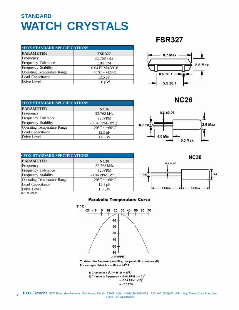
• FOX STANDARD SPECIFICATIONS
6 FOXElectronics 5570 Enterprise Parkway Fort Myers, Florida 33905 USA +001(239)693-0099 FAX +001(239)693-1554 http://www.foxonline.com© 2002 FOX ELECTRONICS
STANDARD
WATCH CRYSTALS
FSR32732.768 kHz
±20PPM-0.04 PPM/(∆ºC)2
-40°C ~ +85°C12.5 pF1.0 µW
PARAMETERFrequencyFrequency ToleranceFrequency StabilityOperating Temperature RangeLoad CapacitanceDrive Level
• FOX STANDARD SPECIFICATIONS
PARAMETERFrequencyFrequency ToleranceFrequency StabilityOperating Temperature RangeLoad CapacitanceDrive Level
• FOX STANDARD SPECIFICATIONS
NC2632.768 kHz
±20PPM-0.04 PPM/(∆ºC)2
-20°C ~ +60°C12.5 pF1.0 µW
Rev. 05/01/02
PARAMETERFrequencyFrequency ToleranceFrequency StabilityOperating Temperature RangeLoad CapacitanceDrive Level
• FOX STANDARD SPECIFICATIONSNC38
32.768 kHz±20PPM
-0.04 PPM/(ƼC)2
-20°C ~ +60°C12.5 pF1.0 µW

7© 2002 FOX ELECTRONICS
FOXElectronics 5570 Enterprise Parkway Fort Myers, Florida 33905 USA +001(239)693-0099 FAX +001(239)693-1554 http://www.foxonline.com
• Inventory Support• Standard Packages• Lowest Pricing• Fox Quality• Technical SupportDISTRIBUTOR STOCKING ITEMS
STANDARD
OSCILLATORS
Rev. 05/01/02
F1100E5V
100PPM0ºC ~ +70ºC
TTL
F5C-2E5V
±100PPM0ºC ~ +70ºC
HCMOS
H5C-2E5V
±100PPM0ºC ~ +70ºC
HCMOS
PARAMETERVoltageFrequency StabilityOperating Temperature RangeOutput
KFO90AT5V
±100PPM-10ºC ~ +70ºC
HCMOS
• FOX STANDARD SPECIFICATIONSF3345
5V±100PPM
-10ºC ~ +70ºCHCMOS
F41003.3V
±100PPM-10ºC ~ +70ºC
HCMOS
F4105/F41063.3V
±50 / ±25PPM-10ºC ~ +70ºC
HCMOS
F1100E / F5C-2E H5C-2E
F3345/F4100/F4105/F4106
KFO90AT
1.0000001.8432002.0000002.4576003.6864004.0000006.0000007.3728008.00000010.00000011.05920012.00000014.31818014.74560016.00000018.43200020.00000024.00000025.00000032.00000033.33300040.00000044.00000048.00000050.00000060.00000064.00000066.66670080.000000
100.000000106.250000125.000000
F4100-018
F4100-0368F4100-040
F4100-100
F4100-143
F4100-160F4100-184F4100-200
F4100-250F4100-320F4100-333F4100-400
F4100-480F4100-500F4100-600
F4100-666
F4100-1062
KFO-018KFO-020
KFO-040
KFO-080KFO-100
KFO-120KFO-143
KFO-160
KFO-200KFO-240
KFO-320
KFO-400
KFO-480KFO-500KFO-600KFO-640KFO-666
F1100E-010F1100E-018F1100E-020F1100E-024F1100E-0368F1100E-040F1100E-060F1100E-073F1100E-080F1100E-100F1100E-115F1100E-120F1100E-143F1100E-147F1100E-160F1100E-184F1100E-200F1100E-240F1100E-250F1100E-320
F1100E-400
F1100E-480F1100E-500
F1100E-640
F1100E-800F1100E-1000
F1100EFREQUENCY (MHz)
H5C2E-010
H5C2E-0368
H5C2E-080
H5C2E-160
H5C2E-200
H5C2E-250H5C2E-320
H5C2E-400
H5C2E-500
H5C2E-640
F5C2E-080F5C2E-100
F5C2E-120
F5C2E-160
F5C2E-200F5C2E-240F5C2E-250F5C2E-320
F5C2E-400
H5C-2E F3345 F4100 KFO90AT
JITO-2 JITO-2 JITO-2 JITO-2 JITO-2 JITO-2 JITO-2 JITO-2 JITO-2 JITO-2 JITO-2 JITO-2 JITO-2 JITO-2 JITO-2 JITO-2 JITO-2 JITO-2 JITO-2 JITO-2 JITO-2 JITO-2 JITO-2 JITO-2 JITO-2 JITO-2 JITO-2 JITO-2 JITO-2 JITO-2 JITO-2 JITO-2
F5C-2E
F3345-018
F3345-080
F3345-120F3345-143
F3345-160
F3345-200F3345-240F3345-250F3345-320
F3345-400
F3345-500F3345-600F3345-640
F4105 /F4106
F4105-143
F4105-200
F4105-250F4105-320
F4105-400F4106-440
F4105-500
F4105-666
F4105-1000F4105-1062F4105-1250

8 FOXElectronics 5570 Enterprise Parkway Fort Myers, Florida 33905 USA +001(239)693-0099 FAX +001(239)693-1554 http://www.foxonline.com© 2002 FOX ELECTRONICS
STANDARD
VCXOs & TCXOsDISTRIBUTOR STOCKING ITEMS
VCS25AXT3.3V
±50PPM±100PPM
-10°C ~ +70°C
FOX801BE3.0V
±2.5PPM±3.0PPM
-30ºC ~ +75ºC
PARAMETERSupply VoltageFrequency StabilityPullabilityOperating Temperature Range
• FOX STANDARD SPECIFICATIONS
1 The voltage control may be disabled by applying 1.50 volts to pin 1. Trimmerless and non-vc parts available on custom order.
Part NumberFOX801BE-100FOX801BE-128FOX801BE-144FOX801BE-160FOX801BE-192FOX801BE-200
Frequency (MHz)10.00000012.80000014.40000016.00000019.20000020.000000
FOX801BE1 (VCTCXO)
1 Other voltages, stabilities, and pullabilities available on custom order.
Part NumberVCS25AXT-0496VCS25AXT-081VCS25AXT-128VCS25AXT-163VCS25AXT-270VCS25AXT-353VCS25AXT-447
Frequency (MHz)4.0960008.192000
12.28800016.38400027.00000035.32800044.736000
VCS25AXT1 (VCXO)
Rev. 05/01/02

9© 2002 FOX ELECTRONICS
FOXElectronics 5570 Enterprise Parkway Fort Myers, Florida 33905 USA +001(239)693-0099 FAX +001(239)693-1554 http://www.foxonline.com
FAST DELIVERY
SUPERIOR QUALITY
CRYSTALS AND OSCILLATORS
Delivery: 5 to 30 working days
Quartz CrystalsHC49U 3 ~ 27 MHz fundamental 30 ~ 60 MHz 3rd overtoneHC49SD 3.579 ~ 64MHz
OscillatorsF1100E 4 ~ 25 MHzF5C-2E 1.000 ~ 50 MHzH5C-2E 1.000 ~ 50 MHzJITO-2 0.340 ~ 300 MHz
Quotes: Call 1-888-GET-2-FOX for price and delivery confirmation.
Let FASTFOX help you with all your "Rush" Requirements 1-888-GET-2-FOX
for Fast Delivery
Look for the Logo
PRODUCT LINE

10 FOXElectronics 5570 Enterprise Parkway Fort Myers, Florida 33905 USA +001(239)693-0099 FAX +001(239)693-1554 http://www.foxonline.com© 2002 FOX ELECTRONICS
IMPORTANTWhen ordering any non-standard crystals, please specify series or parallel resonance. If parallel, the load capacitance (CL) needs to be specified in picofarads _____pF.
QUARTZ CRYSTAL
SELECTION GUIDE
FASTFOX is a quick delivery service. Check with Fox Customer Service for available frequencies.
Frequency RangeFrequency ToleranceFrequency StabilityTemperature Range
Key Features
Catalog Pages
PRODUCT FE
7.1124 ~ 160.000 MHz±50 PPM ~ ±20 PPM±50 PPM ~ ±15 PPM-10°C ~ +60°C to-40ºC ~ +85ºC• 7.5 x 5mm• 1.4mm Height Max• Low Cost - Resin Sealed• Fundamental to 50 MHz• 2 Additional Footprints (FH, FL)
Page 15
FD
9.8304 ~ 160.000 MHz±50 PPM ~ ±5 PPM±50 PPM ~ ±3 PPM-10°C ~ +60°C to-40ºC ~ +85ºC• 7.5 x 5mm• 1.1mm Height Max• Fundamental to 50 MHz• Seam Sealed
Page 16
FC
3.200 ~ 7.200 MHz±50 PPM ~ ±20 PPM±50 PPM ~ ±15 PPM-10°C ~ +60°C to-40ºC ~ +85ºC• 11.8 x 5.5mm• 2.5mm Height Max• Low Cost - Resin Sealed
Page 17
FPX
3.579545 ~ 90.000 MHz±50 PPM ~ ±20 PPM±100 PPM ~ ±20 PPM-10°C ~ +60°C to-40ºC ~ +85ºC• Low Cost• Plastic Encapsulated
Page 18S
tock
ing
Std
.
HC49SD
3.200 ~ 70.000 MHz±50 PPM ~ ±10 PPM±50 PPM ~ ±5 PPM-10°C ~ +60°C to-40ºC ~ +85ºC• Low Cost• Fundamental to 50 MHz
Page 19
Sto
ckin
g S
td.
Sto
ckin
g S
td.
• SURFACE MOUNT CRYSTALS
Frequency RangeFrequency ToleranceFrequency StabilityTemperature RangeKey Features
Catalog Pages
FX532 Series
12.000 ~ 67.000 MHz±50 PPM ~ ±10 PPM±50 PPM ~ ±10 PPM-10°C ~ +60°C to -40ºC ~ +85ºC• 5 x 3.2mm• 1.0mm Height Max• Fundamental to 67 MHz• Low Cost• Resin Sealed or Seam Welded
Page 12
FX325B
16.000 ~ 50.000 MHz±50 PPM ~ ±20 PPM±50 PPM ~ ±20 PPM-10°C ~ +60°C to -40ºC ~ +85ºC• 3.2 x 2.5mm• 1.0mm Height Max• Low Cost• Fundamental to 50 MHz• Resin Sealed or Seam Sealed
Page 11
PRODUCT FQA
11.0592 ~ 67.000 MHz±50 PPM ~ ±20 PPM±100 PPM ~ ±20 PPM-10°C ~ +60°C to -40ºC ~ +85ºC• 6 x 3.5mm• 1.4mm Height Max• Low Cost - Resin Sealed• Fundamental to 40 MHz
Page 13
FMB
10.368 ~ 67.000 MHz±50 PPM ~ ±5 PPM±100 PPM ~ ±3 PPM-10°C ~ +60°C to -40ºC ~ +85ºC• 6 x 3.5mm• 1.1mm Height Max• Fundamental to 67 MHz• Seam Sealed
Page 14
• THRU-HOLE CRYSTALS / WATCH CRYSTALS
PRODUCT
Frequency RangeFrequency ToleranceFrequency StabilityTemperature RangeKey Features
Catalog Pages
WATCH CRYSTALS
32.768 kHz±20PPM-0.04PPM / (∆°C)2
-20°C ~ +60°C / -40ºC ~ +85ºC• Miniature Pkgs.• Long Term Stability
Pages 23 - 25
HC49S
3.200 ~ 70.000 MHz±50 PPM ~ ±10 PPM±50PPM ~ ±5 PPM-10°C ~ +70°C to -40ºC ~ +85ºC• 3.6mm Profile• Low Cost• Resistance Weld• Fundamental to 50 MHz
Page 20
HC80U
3.579545 ~ 200.000 MHz±30 PPM ~ ±5 PPM±50 PPM ~ ±3 PPM-20°C ~ +70°C to -40ºC ~ +70ºC• High Frequency Range• Fundamental to 50 MHz
Page 21
HC49U
1.8432 ~ 180.000 MHz±30 PPM ~ ±5 PPM±50 PPM ~ ±3 PPM-20°C ~ +70°C to -40ºC ~ +85ºC• Low Cost• Fundamental to 40 MHz
Page 22
Sto
ckin
g S
td.
Sto
ckin
g S
td.
CR
YSTA
LS

11© 2002 FOX ELECTRONICS
FOXElectronics 5570 Enterprise Parkway Fort Myers, Florida 33905 USA +001(239)693-0099 FAX +001(239)693-1554 http://www.foxonline.com
See page 27 for tape and reel specifications.
CERAMIC SMD CRYSTAL
FX325BFEATURES• Low Cost• Fundamental to 50 MHz• Tape and Reel (3,000 pcs. STD)
1 Other tolerances, stabilities & operating temperature ranges available. Consult Fox CustomerService for specific requirements.All specifications subject to change without notice. Rev. 05/01/02
PARAMETERSFrequency RangeFrequency Tolerance @ 25ºCFrequency Stability, ref @ 25ºC Over Operating Temp RangeTemperature Range
Operating (TOPR)Storage (TSTG)
Equivalent Series ResistanceShunt Capacitance (Co)Load Capacitance (CL)
Drive LevelAging per year
16.000 ~ 50.000 MHz±50 PPM
±50 PPM
-10ºC ~ +60ºC-40ºC ~ +85ºC
90 Ω7.0 pF
10 pF ~ Series(Customer Specified)
0.1 mW±5 PPM
• STANDARD SPECIFICATIONS1
All dimensions are in millimeters.
OPTIONS• Tolerances to < 20 PPM• Stabilities to < 20 PPM• Temperatures to -40ºC ~ +85ºC• 0.8mm Height Max
CR
YS
TALS
MAX (unless otherwise noted)

12 FOXElectronics 5570 Enterprise Parkway Fort Myers, Florida 33905 USA +001(239)693-0099 FAX +001(239)693-1554 http://www.foxonline.com© 2002 FOX ELECTRONICS
CR
YS
TALS
All dimensions are in millimeters.
CERAMIC SMD CRYSTALS
FX532 SERIESFEATURES• Low Cost• Fundamental to 67 MHz• Resin Sealed or Seam Sealed• Tape and Reel (2,000 pcs. STD)
1 Other tolerances, stabilities & operating temperature ranges available. Consult Fox CustomerService for specific requirements.2 Inclusive of tolerance at 25ºCAll specifications subject to change without notice. Rev. 05/01/02
PARAMETERSFrequency RangeFrequency Tolerance, Ta=25ºC 12.000 ~ 40.000 MHz 40.000+ ~ 67.000 MHzFrequency Stability 12.000 ~ 40.000 MHz (ref. @ 25ºC) 40.000+ ~ 67.000 MHzTemperature Range
Operating (TOPR)Storage (TSTG)
Shunt Capacitance (Co)Load Capacitance (CL)
Drive LevelAging per year
12.000 ~ 67.000 MHz
±50PPMSee Stability
±50 PPM±100 PPM 2
-10ºC ~ +60ºC-40ºC ~ +85ºC
7.0 pF10 pF ~ Series
(Customer Specified)0.1 mW±5 PPM
• STANDARD SPECIFICATIONS1
See page 27 for tape and reel specifications.
12.000 ~ 14.00014.000+ ~ 16.00016.000+ ~ 67.000
Frequency Range(MHz)
FundamentalFundamentalFundamental
1409060
Operating Mode Max ESR Ω
OPTIONS• Tolerances to < 10 PPM• Stabilities to < 10 PPM• Temperatures to -40ºC ~ +85ºC
MAX (unless otherwise noted)
13© 2002 FOX ELECTRONICS
FOXElectronics 5570 Enterprise Parkway Fort Myers, Florida 33905 USA +001(239)693-0099 FAX +001(239)693-1554 http://www.foxonline.com
CR
YS
TALSFEATURES
• Low Cost• Fundamental to 40 MHz• Resin Sealed• Tape and Reel (2,000 pcs.STD)
1 Other stabilities & operating temperature ranges available. Consult Fox Customer Service forspecific requirements.2 Inclusive of tolerance at 25ºC.All specifications subject to change without notice. Rev. 05/01/02
CERAMIC RESIN SEALED SMD CRYSTAL
FQA
See page 27 for tape and reel specifications.
PARAMETERSFrequency RangeFrequency Stability Over Operating Temp RangeTemperature Range
Operating (TOPR)Storage (TSTG)
Shunt Capacitance (Co)Load Capacitance (CL)
Drive LevelAging per year
11.0592 ~ 67.000 MHz
±100 PPM 2
-10ºC ~ +60ºC-40ºC ~ +85ºC
7.0 pF10 pF ~ Series
(Customer Specified)0.1 mW±5 PPM
• STANDARD SPECIFICATIONS1
11.0592 ~ 12.00012.000+ ~ 16.00016.000+ ~ 40.00040.000 ~ 67.000
Frequency Range(MHz)
FundamentalFundamentalFundamental
3rd OT
80604070
Operating Mode Max ESR Ω
All dimensions are in millimeters.
OPTIONS• Tolerances to < 20 PPM• Stabilities to < 20 PPM• Temperatures to -40ºC ~ +85ºC
MAX (unless otherwise noted)

14 FOXElectronics 5570 Enterprise Parkway Fort Myers, Florida 33905 USA +001(239)693-0099 FAX +001(239)693-1554 http://www.foxonline.com© 2002 FOX ELECTRONICS
CR
YS
TALS
FEATURES• Fundamental to 40 MHz• Seam Sealed• Tape and Reel (2,000 pcs. STD)
1 Other tolerances, stabilities & operating temperature ranges available. Consult Fox CustomerService for specific requirements.2 Inclusive of tolerance at 25ºC.All specifications subject to change without notice. Rev. 05/01/02
CERAMIC SEAM SEALED SMD CRYSTAL
FMB
PARAMETERSFrequency RangeFrequency Stability Over Operating Temp RangeTemperature Range
Operating (TOPR)Storage (TSTG)
Shunt Capacitance (Co)Load Capacitance (CL)
Drive LevelAging per year
• STANDARD SPECIFICATIONS1
10.368 ~ 67.000 MHz
±100 PPM 2
-10ºC ~ +60ºC-40ºC ~ +85ºC
7.0 pF10 pF ~ Series
(Customer Specified)0.1 mW±5 PPM
See page 27 for tape and reel specifications.
10.368 ~ 12.00012.000+ ~ 16.00016.000+ ~ 40.00040.000+ ~ 67.000
Frequency Range(MHz)
FundamentalFundamentalFundamental
3rd OT
80604070
Operating Mode Max ESR Ω
All dimensions are in millimeters.
MAX (unless otherwise noted)
OPTIONS• Tolerances to < 5 PPM• Stabilities to < 3 PPM• Temperatures to -40ºC ~ +85ºC

15© 2002 FOX ELECTRONICS
FOXElectronics 5570 Enterprise Parkway Fort Myers, Florida 33905 USA +001(239)693-0099 FAX +001(239)693-1554 http://www.foxonline.com
CR
YS
TALSFEATURES
• Low Cost• High Frequency Range• Fundamental to 50 MHz (BT Cut)• Resin Sealed• Tape and Reel (2,000 pcs. STD)
1 Other stabilities & operating temperature ranges available. Consult Fox Customer Service forspecific requirements.All specifications subject to change without notice. Rev. 05/01/02
CERAMIC RESIN SEALED SMD CRYSTAL
FE
See page 27 for tape and reel specifications.
All dimensions are in millimeters.
7.1124 ~ 8.0008.000+ ~ 16.00016.000+ ~ 50.00028.000 ~ 84.000
84.000+ ~ 160.000
Frequency Range(MHz)
FundamentalFundamentalFundamental
3rd OT5th OT
8060406080
Operating Mode Max ESR Ω
• STANDARD SPECIFICATIONS1
PARAMETERSFrequency RangeFrequency Tolerance @ 25ºCFrequency Stability, ref @ 25ºC Over Operating Temp RangeTemperature Range
Operating (TOPR)Storage (TSTG)
Shunt Capacitance (Co)Load Capacitance (CL)
Drive LevelAging per year
7.1124 ~ 160.000 MHz±50 PPM
±50PPM
-10ºC ~ +60ºC-40ºC ~ +85ºC
7.0 pF10 pF ~ Series
(Customer Specified)0.5 mW±5 PPM
MAX (unless otherwise noted)
OPTIONS• Tolerances to < 20 PPM• Stabilities to < 15 PPM• Temperatures to -40ºC ~ +85ºC• 1.4mm Height Max• 2 Additional Footprints (FH,FL)

16 FOXElectronics 5570 Enterprise Parkway Fort Myers, Florida 33905 USA +001(239)693-0099 FAX +001(239)693-1554 http://www.foxonline.com© 2002 FOX ELECTRONICS
CR
YS
TALS
FEATURES• High Frequency Range• Fundamental to 50 MHz (BT Cut)• Seam Sealed• Tape and Reel (3,000 pcs. STD)
1 Other tolerances, stabilities & operating temperature ranges available. Consult Fox Customer Service forspecific requirements.All specifications subject to change without notice. Rev. 05/01/02
CERAMIC SEAM SEALED SMD CRYSTAL
FD
PARAMETERSFrequency RangeFrequency Tolerance @ 25ºCFrequency Stability, ref @ 25ºC Over Operating Temp RangeTemperature Range
Operating (TOPR)Storage (TSTG)
Shunt Capacitance (Co)Load Capacitance (CL)
Drive LevelAging per year
9.8304 ~ 160.000 MHz±50 PPM
±50 PPM
-10ºC ~ +60ºC-40ºC ~ +85ºC
7.0 pF10 pF ~ Series
(Customer Specified)0.5 mW±5 PPM
• STANDARD SPECIFICATIONS1
See page 27 for tape and reel specifications.
9.8304 ~ 16.00016.000+ ~ 50.00028.000 ~ 84.000
84.000 ~ 160.000
Frequency Range(MHz)
FundamentalFundamental
3rd OT5th OT
60406080
Operating Mode Max ESR Ω
All dimensions are in millimeters.
MAX (unless otherwise noted)
OPTIONS• Tolerances to < 5 PPM• Stabilities to < 3 PPM• Temperatures to -40ºC ~ +85ºC

17© 2002 FOX ELECTRONICS
FOXElectronics 5570 Enterprise Parkway Fort Myers, Florida 33905 USA +001(239)693-0099 FAX +001(239)693-1554 http://www.foxonline.com
CR
YS
TALSFEATURES
• Low Cost• Resin Sealed• Tape and Reel (1,000 pcs. STD)
All specifications subject to change without notice. Rev. 05/01/02
CERAMIC RESIN SEALED SMD CRYSTAL
FC
• STANDARD SPECIFICATIONSPARAMETERSFrequency RangeFrequency Tolerance @ 25ºCFrequency Stability, ref @ 25ºC Over Operating Temp RangeTemperature Range
Operating (TOPR)Storage (TSTG)
Shunt Capacitance (Co)Load Capacitance (CL)
Drive LevelAging per year
3.200 ~ 7.200 MHz±50 PPM
±50 PPM
-10ºC ~ +60ºC-40ºC ~ +85ºC
7.0 pF10 pF ~ Series
(Customer Specified)0.1 mW±5 PPM
See page 27 for tape and reel specifications.
3.200 ~ 3.4993.499+ ~ 3.9993.999+ ~ 4.3994.399+ ~ 4.8994.899+ ~ 5.9995.999+ ~ 6.9996.999+ ~ 7.200
Frequency Range(MHz)
FundamentalFundamentalFundamentalFundamentalFundamentalFundamentalFundamental
200140120100806050
Operating Mode Max ESR Ω
All dimensions are in millimeters.
MAX (unless otherwise noted)
OPTIONS• Tolerances to < 20 PPM• Stabilities to < 15 PPM• Temperatures to -40ºC ~ +85ºC
18 FOXElectronics 5570 Enterprise Parkway Fort Myers, Florida 33905 USA +001(239)693-0099 FAX +001(239)693-1554 http://www.foxonline.com© 2002 FOX ELECTRONICS
CR
YS
TALS
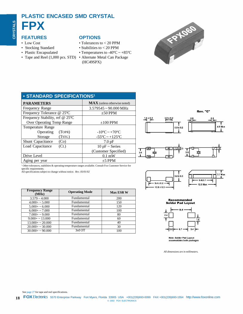
FEATURES• Low Cost• Stocking Standard• Plastic Encapsulated• Tape and Reel (1,000 pcs. STD)
PLASTIC ENCASED SMD CRYSTAL
FPX
See page 27 for tape and reel specifications.
1 Other tolerances, stabilities & operating temperature ranges available. Consult Fox Customer Service forspecific requirements.All specifications subject to change without notice. Rev. 05/01/02
3.579545 ~ 90.000 MHz±50 PPM
±100 PPM
-10ºC ~ +70ºC-55ºC ~ +125ºC
7.0 pF10 pF ~ Series
(Customer Specified)0.1 mW±5 PPM
PARAMETERSFrequency RangeFrequency Tolerance @ 25ºCFrequency Stability, ref @ 25ºC Over Operating Temp RangeTemperature Range
Operating (TOPR)Storage (TSTG)
Shunt Capacitance (Co)Load Capacitance (CL)
Drive LevelAging per year
• STANDARD SPECIFICATIONS1
3.579 ~ 4.0004.000+ ~ 5.0005.000+ ~ 6.0006.000+ ~ 7.0007.000+ ~ 9.000
9.000+ ~ 13.00013.000+ ~ 20.00020.000+ ~ 30.00030.000+ ~ 90.000
Frequency Range(MHz)
FundamentalFundamentalFundamentalFundamentalFundamentalFundamentalFundamentalFundamental
3rd OT
20015012010080604030100
Operating Mode Max ESR Ω
MAX (unless otherwise noted)
OPTIONS• Tolerances to < 20 PPM• Stabilities to < 20 PPM• Temperatures to -40ºC ~ +85ºC• Alternate Metal Can Package (HC49SPX)
All dimensions are in millimeters.

19© 2002 FOX ELECTRONICS
FOXElectronics 5570 Enterprise Parkway Fort Myers, Florida 33905 USA +001(239)693-0099 FAX +001(239)693-1554 http://www.foxonline.com
CR
YS
TALS
See page 27 for tape and reel specifications.
FEATURES• Low Cost• Stock Standard• Fundamental to 50 MHz (BTCut)• Tape and Reel (1,000 pcs. STD)
OPTIONS• Tolerances to < 10 PPM• Stabilities to < 5 PPM• Temperatures to -40ºC ~ -85ºC• 4 Pad HC49SPX (Alternate toFPX)• 3.2mm Height Max (HC49SSD)
1 Other tolerances, stabilities & operating temperature ranges available. Consult Fox Customer Service forspecific requirements.All specifications subject to change without notice. Rev. 05/01/02
RESISTANCE WELD SMD CRYSTAL
HC49SD
3.200 ~ 70.000 MHz±50 PPM
±50 PPM
-10ºC ~ +70ºC-40ºC ~ +85ºC
7.0 pF10 pF ~ Series
(Customer Specified)0.5 mW±5 PPM
Frequency RangeFrequency Tolerance @ 25ºCFrequency Stability, ref @ 25ºC Over Operating Temp RangeTemperature Range
Operating (TOPR)Storage (TSTG)
Shunt Capacitance (Co)Load Capacitance (CL)
Drive LevelAging @ 25ºC; per year
• STANDARD SPECIFICATIONS1
PARAMETERS
3.200 ~ 3.5003.500+ ~ 4.0004.000+ ~ 5.0005.000+ ~ 6.0006.000+ ~ 7.0007.000+ ~ 9.000
9.000+ ~ 13.00013.000+ ~ 20.00020.000+ ~ 50.00027.000 ~ 70.000
Frequency Range(MHz)
FundamentalFundamentalFundamentalFundamentalFundamentalFundamentalFundamentalFundamentalFundamental
3rd OT
30020015012010080604030100
Operating Mode Max ESR Ω
All dimensions are in millimeters.
MAX (unless otherwise noted)

20 FOXElectronics 5570 Enterprise Parkway Fort Myers, Florida 33905 USA +001(239)693-0099 FAX +001(239)693-1554 http://www.foxonline.com© 2002 FOX ELECTRONICS
RESISTANCE WELD THRU-HOLE CRYSTAL
HC49S
1 Other tolerances, stabilities & operating temperature ranges available. Consult Fox Customer Service forspecific requirements.All specifications subject to change without notice. Rev. 05/01/02
OPTIONS• Tolerances to < 10 PPM• Stabilities to < 5 PPM• Temperatures to -40ºC ~+85ºC• 2.5mm Height Max(HC49SS)
FEATURES• Low Cost• Stocking Standard• Fundamental to 50 MHz (BTCut)• Resistance Weld
PARAMETERSFrequency RangeFrequency Tolerance @ 25ºCFrequency Stability, ref @ 25ºC Over Operating Temp RangeTemperature Range
Operating (TOPR)Storage (TSTG)
Shunt Capacitance (Co)Load Capacitance (CL)
Drive LevelAging per year
3.200 ~ 70.000 MHz±50 PPM
±50 PPM
-20ºC ~ +70ºC-40ºC ~ +85ºC
7.0 pF10 pF ~ Series
(Customer Specified)0.5 mW±5 PPM
• STANDARD SPECIFICATIONS1
3.200 ~ 3.5003.500+ ~ 4.0004.000+ ~ 5.0005.000+ ~ 6.0006.000+ ~ 7.0007.000+ ~ 9.000
9.000+ ~ 13.00013.000+ ~ 20.00020.000+ ~ 50.00027.000 ~ 70.000
Frequency Range(MHz)
FundamentalFundamentalFundamentalFundamentalFundamentalFundamentalFundamentalFundamentalFundamental
3rd OT
30020015012010080604030100
Operating Mode Max ESR Ω
All dimensions are in millimeters.
MAX (unless otherwise noted)
CR
YS
TALS

21© 2002 FOX ELECTRONICS
FOXElectronics 5570 Enterprise Parkway Fort Myers, Florida 33905 USA +001(239)693-0099 FAX +001(239)693-1554 http://www.foxonline.com
FEATURES• High Frequency Range• Fundamental to 50 MHz• Resistance Weld
RESISTANCE WELD THRU-HOLE CRYSTAL
HC80U
1 Other tolerances, stabilities & operating temperature ranges available. Consult Fox Customer Service forspecific requirements.All specifications subject to change without notice. Rev. 05/01/02
PARAMETERSFrequency RangeFrequency Tolerance @ 25ºCFrequency Stability, ref @ 25ºC Over Operating Temp RangeTemperature Range
Operating (TOPR)Storage (TSTG)
Shunt Capacitance (Co)Load Capacitance (CL)
Drive LevelAging per year
3.579545 ~ 200.000 MHz±30 PPM
±50 PPM
-20ºC ~ +70ºC-40ºC ~ +85ºC
7.0 pF10 pF ~ Series
(Customer Specified)1.0 mW±3 PPM
• STANDARD SPECIFICATIONS1
All dimensions are in millimeters.
3.579545 ~ 4.0004.000+ ~ 5.0005.000+ ~ 6.0006.000+ ~ 7.0007.000+ ~ 8.000
8.000+ ~ 10.00010.000+ ~ 11.00011.000+ ~ 50.00025.000 ~ 65.00060.000 ~ 130.000
130.000+ ~ 200.000
Frequency Range(MHz)
FundamentalFundamentalFundamentalFundamentalFundamentalFundamentalFundamentalFundamental
3rd OT5th OT7th OT
30025018012010090604060100150
Operating Mode Max ESR Ω
MAX (unless otherwise noted)
OPTIONS• Tolerances to < 5 PPM• Stabilities to < 3 PPM• Temperatures to -40ºC ~ -85ºC• SMD Gullwing (HC80UW)
CR
YS
TALS

22 FOXElectronics 5570 Enterprise Parkway Fort Myers, Florida 33905 USA +001(239)693-0099 FAX +001(239)693-1554 http://www.foxonline.com© 2002 FOX ELECTRONICS
CR
YS
TALS
RESISTANCE WELD THRU-HOLE CRYSTAL
HC49U
1 Other tolerances, stabilities & operating temperature ranges available. Consult Fox Customer Service forspecific requirements.All specifications subject to change without notice. Rev. 05/01/02
PARAMETERSFrequency RangeFrequency Tolerance @ 25ºCFrequency Stability, ref @ 25ºC Over Operating Temp RangeTemperature Range
Operating (TOPR)Storage (TSTG)
Shunt Capacitance (Co)Load Capacitance (CL)
Drive Level1.8432 ~ 3.000 MHz3.000+ ~ 180.000 MHz
Aging per year
1.8432 ~ 180.000 MHz±30 PPM
±50 PPM
-20ºC ~ +70ºC-40ºC ~ +85ºC
7.0 pF10 pF ~ Series
(Customer Specified)
2.0 mW1.0 mW±5 PPM
• STANDARD SPECIFICATIONS1
1.8432 ~ 2.0002.000+ ~ 2.4002.400+ ~ 3.0003.000+ ~ 3.2003.200+ ~ 3.7003.700+ ~ 4.2004.200+ ~ 4.9004.900+ ~ 5.0005.000+ ~ 6.0006.000+ ~ 8.0008.000+ ~ 10.00010.000+ ~ 12.50012.500+ ~ 16.00016.000+ ~ 40.00023.000+ ~ 75.00060.000 ~ 110.000110.000 ~ 180.000
Frequency Range(MHz)
FundamentalFundamentalFundamentalFundamentalFundamentalFundamentalFundamentalFundamentalFundamentalFundamentalFundamentalFundamentalFundamentalFundamental
3rd OT5th OT7th OT
75050030020012010070555040353025204080120
Operating Mode Max ESR Ω
All dimensions are in millimeters.
MAX (unless otherwise noted)
FEATURES• Low Cost• Stocking Standard• High Frequency Range• Fundamental to 40 MHz• Resistance Weld
OPTIONS• Tolerances to < 5 PPM• Stabilities to < 3 PPM• Temperatures to -40ºC ~ -85ºC• Mylar Spacer• Vinyl Sleeve• Third Lead• SMD Gullwing (HC49UW)

23© 2002 FOX ELECTRONICS
FOXElectronics 5570 Enterprise Parkway Fort Myers, Florida 33905 USA +001(239)693-0099 FAX +001(239)693-1554 http://www.foxonline.com
SMD TUNING FORK
FSXFEATURES• Extremely Small Size• Low Cost• 1.4mm Height Max• Tape and Reel (3,000 pcs. STD)
PARAMETERSFrequency RangeFrequency Tolerance @ 25ºCFrequency Stability, ref @ 25ºCTemperature Range
Operating (TOPR)Storage (TSTG)
Equivalent Series ResistanceLoad Capacitance (CL)Insulation Resistance @ 100VDC
Drive LevelAging
32.768 kHz±20 PPM
-0.04PPM/(ƼC)2
-40ºC ~ +85ºC-40ºC ~ +85ºC
65 kΩ7 pF, 12.5pF
500 MΩ0.1 µW±3 PPM
• STANDARD SPECIFICATIONS
See page 27 for tape and reel specifications.
All specifications subject to change without notice. Rev. 05/01/02
All dimensions are in millimeters.
MAX (unless otherwise noted)
WA
TCH
CR
YS
TALS

24 FOXElectronics 5570 Enterprise Parkway Fort Myers, Florida 33905 USA +001(239)693-0099 FAX +001(239)693-1554 http://www.foxonline.com© 2002 FOX ELECTRONICS
MAX (unless otherwise noted)
WA
TCH
CR
YS
-TA
LS
FEATURES• Miniature Package• 2.5mm Height• Long Term Stability• Tape and Reel (3,000 pcs. STD)
All specifications subject to change without notice. Rev. 05/01/02
SMD TUNING FORK
FSR327
32.768 kHz±20 PPM
-0.04 PPM / (ƼC)2
+20ºC ~ +30ºC-40ºC ~ +85ºC-55ºC ~ +125ºC
50 kΩ12.5 pF (Standard)
6 pF (Optional)500 MΩ1.0 µW±3 PPM
PARAMETERSFrequencyFrequency Tolerance @ 25ºCFrequency Stability Temperature CoefficientTemperature Range
Turnover (TO)Operating (TOPR)Storage (TSTG)
Equivalent Series Resistance (RS)Load Capacitance (CL)
Insulation Resistance @ 100VDCDrive LevelAging per year
• STANDARD SPECIFICATIONS
See page 27 for tape and reel specifications.
All dimensions are in millimeters.
25© 2002 FOX ELECTRONICS
FOXElectronics 5570 Enterprise Parkway Fort Myers, Florida 33905 USA +001(239)693-0099 FAX +001(239)693-1554 http://www.foxonline.com
WA
TCH
CR
YS
-TA
LSTHRU-HOLE TUNING FORK
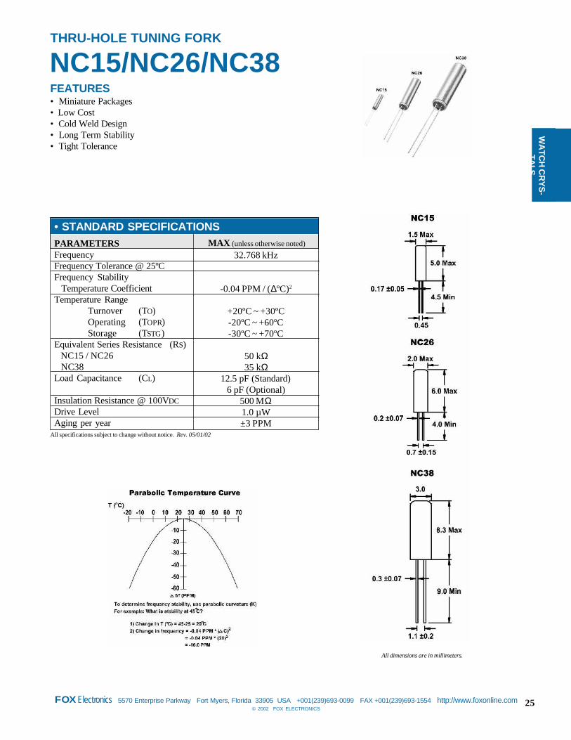
FEATURES• Miniature Packages• Low Cost• Cold Weld Design• Long Term Stability• Tight Tolerance
NC15/NC26/NC38
All specifications subject to change without notice. Rev. 05/01/02
32.768 kHz
-0.04 PPM / (ƼC)2
+20ºC ~ +30ºC-20ºC ~ +60ºC-30ºC ~ +70ºC
50 kΩ35 kΩ
12.5 pF (Standard)6 pF (Optional)
500 MΩ1.0 µW±3 PPM
PARAMETERSFrequencyFrequency Tolerance @ 25ºCFrequency Stability Temperature CoefficientTemperature Range
Turnover (TO)Operating (TOPR)Storage (TSTG)
Equivalent Series Resistance (RS) NC15 / NC26 NC38Load Capacitance (CL)
Insulation Resistance @ 100VDCDrive LevelAging per year
• STANDARD SPECIFICATIONS
All dimensions are in millimeters.
MAX (unless otherwise noted)

26 FOXElectronics 5570 Enterprise Parkway Fort Myers, Florida 33905 USA +001(239)693-0099 FAX +001(239)693-1554 http://www.foxonline.com© 2002 FOX ELECTRONICS
Fox
Ele
ctro
nic
s P
art
Des
crip
tio
n1
Gu
ide
for
Cry
stal
s
(###
#.##
####
)
Sect
ion
A
A ±
100
ppm
B ±
50
ppm
C ±
30p
pmD
± 2
5ppm
E ±
20p
pmF
± 1
5ppm
G ±
12p
pmH
± 1
0ppm
J ±
7.5
ppm
K ±
7pp
mL
± 5
ppm
M ±
4pp
mN
± 3
ppm
P ±
2.5
ppm
R ±
2pp
mS
± 1
.5pp
mT
± 1
ppm
U ±
0.5
ppm
V ±
200
ppm
W ±
70p
pmX
± 1
00pp
m O
VE
RA
LL
Y ±
100
0ppm
Z ±
Oth
er
Ope
ratin
g Te
mp.
Ran
ge
A =
0º t
o +
50ºC
C =
0º t
o +
70ºC
B =
-10
º to
+50
ºCD
= -1
0º to
+60
ºCE
= -
10º t
o +
70ºC
F =
-20º
to +
70ºC
Z =
-20
º to
+75
ºCG
= -3
0º to
+70
ºCH
= -3
0º to
+75
ºCJ
= -
30º t
o +
80ºC
K =
-30º
to +
85ºC
L =
-35
º to
+80
ºCV
= -3
5º to
+85
ºCM
= -
40º t
o +
85ºC
N =
-40º
to +
90ºC
P =
-40
º to
+10
5ºC
U =
-55º
to +
85ºC
R =
-55
º to
+10
0ºC
S =
-55
º to
+10
5ºC
T =
-55
º to
+12
5ºC
W =
Oth
er
Cir
cuit
Con
diti
on
000
= S
erie
s06
0 =
6pF
075
= 7
.5pF
080
= 8
pF10
0 =
10p
F10
5 =
10.
5pF
120
= 1
2pF
125
= 1
2.5p
F13
0 =
13p
F15
0 =
15p
F16
0 =
16p
F18
0 =
18p
F20
0 =
20p
F22
0 =
22p
F24
0 =
24p
F27
0 =
27p
F30
0 =
30p
F32
0 =
32p
F33
0 =
33p
F50
0 =
50p
F99
9 =
Oth
er
Osc
illa
tion
Mod
e
1 =
Fun
dam
enta
l3
= 3
rd O
vert
one
5 =
5th
Ove
rton
e7
= 7
th O
vert
one
9 =
9th
Ove
rton
e0
= B
T C
ut F
unda
men
tal
SMD
Pac
kagi
ng
0 =
Tap
e/R
eel*
250
= 2
5050
0 =
500
1000
= 1
000
Tape
Onl
y =
Tap
e O
nly
Cus
tom
C =
Cus
tom
Plea
se a
ttach
draw
ing
and/
orad
diti
onal
ele
ctri
cal
spec
s fo
r our
engi
neer
ing
depa
rtm
ent.
Val
ue A
dded
A =
3rd
LE
AD
Sol
dere
dB
= 3
rd L
EA
D W
elde
dC
= 3
rd B
ase
Lea
dD
= S
leev
eE
= F
lat S
pace
rF
= R
ibbe
d Sp
acer
L =
For
med
Lea
dsM
= S
peci
al M
arki
ngN
= C
ut B
ase
P =
Cut
Top
S =
Bul
kT
= T
rays
V =
Rad
ial T
ape/
Stra
ight
W =
Rad
ial T
ape/
Cri
mp
Y =
Filt
er B
oxZ
= S
MD
Tap
eZ
8 =
SM
D 8
mm
Tap
e (F
PX O
nly)
Z12
- SM
D 1
2mm
Tap
e (F
PX a
nd F
PX R
ev. C
Not
es:
1 Fox
uni
que
part
num
bers
for
non
-sta
ndar
ds a
re r
ando
mly
gen
erat
ed b
ased
on
the
elem
ents
of
th
e pa
rt d
escr
iptio
n in
a f
orm
at: #
## -
Fre
quen
cy -
Ran
dom
# (
099-
22.1
184-
3978
9 is
Fox
uni
que
pa
rt n
umbe
r).
2 All
com
bina
tion
s ar
e no
t po
ssib
le.
*
0 =
Tap
e/R
eel a
ssum
es th
at n
o qu
antit
y pe
r re
el w
as s
peci
fied
: th
eref
ore,
the
Fox
Prod
uctio
n SM
D
Ree
l Qua
ntiti
es li
st a
pplie
s. F
or a
ny o
ther
qua
ntiti
es s
peci
fied
a b
roke
n re
el c
harg
e w
ill a
pply
.
Fox
Prod
uctio
n SM
D R
eel
Qua
ntiti
es
FD3K
FE/F
H/F
L2K
FC1K
FM/F
MB
2KFP
X1K
FSM
2KH
C49
SD1K
HC
49SS
D1K
FST
/FSR
3KFQ
A2K
FSX
3KFX
325
3KFX
532A
2K
1M
ake
Sel
ectio
n fr
omP
rodu
ct F
amily
in F
ox C
atal
og o
rF
oxon
line.
com
For
Exa
mpl
e: H
C49
SD
2F
req
uen
cy M
Hz
Cus
tom
er F
ills
In
3To
lera
nce
2
Pic
k fr
omS
ectio
n A
4S
tab
ility
2
Pic
k fr
omS
ectio
n A
5O
per
atin
gTe
mp
2
6C
ircu
itC
on
dit
ion
7O
scill
atio
nM
od
e
8S
MD
Pac
kag
ing
9F
ox
Use
10/1
1V
alu
eA
dd
ed
12C
ust
om

27© 2002 FOX ELECTRONICS
FOXElectronics 5570 Enterprise Parkway Fort Myers, Florida 33905 USA +001(239)693-0099 FAX +001(239)693-1554 http://www.foxonline.com
SURFACE MOUNT CRYSTALS
TAPE AND REEL SPECIFICATIONS
1 Standard reel quantity.
TAPE SPECIFICATIONS (millimeters)MODELFX325BFX532 SeriesFQAFMBFEFDFCFPXHC49SDFSXFSR
A∅ 1.5∅ 1.5∅ 1.5∅ 1.5∅ 1.5∅ 1.5∅ 1.5∅ 1.5∅ 1.5∅ 1.5∅ 1.5
B4.04.04.04.04.04.04.04.04.04.04.0
C4.08.08.08.08.08.012.012.012.08.08.0
D3.55.55.55.57.57.511.511.511.57.57.5
E8.012.012.012.016.016.024.024.024.016.016.0
F1.31.951.91.92.31.72.95.54.81.62.7
STD QTY1
3,0001,000 / 2,000
2,0002,0002,0003,0001,0002,0001,0003,0003,000
REEL SPECIFICATIONS (millimeters)MODELFX325BFX532 SeriesFQAFMBFEFDFCFPXHC49SDFSXFSR
G2.02.02.02.02.02.02.02.02.02.02.0
H∅ 13∅ 13∅ 13∅ 13∅ 13∅ 13∅ 13∅ 13∅ 13∅ 13∅ 13
I∅ 21∅ 21∅ 21∅ 21∅ 21∅ 21∅ 21∅ 21∅ 21∅ 21∅ 21
J∅ 60∅ 80∅ 80∅ 80∅ 80∅ 80∅ 80∅ 100∅ 80∅ 50
∅ 50/100
K∅ 180
∅ 178 / ∅ 250∅ 250∅ 250∅ 250∅ 250∅ 250∅ 250∅ 330∅ 330∅ 330
L9.013.513.513.517.517.525.525.525.516.416.4
M1.22.02.02.02.02.02.02.02.02.02.0
28 FOXElectronics 5570 Enterprise Parkway Fort Myers, Florida 33905 USA +001(239)693-0099 FAX +001(239)693-1554 http://www.foxonline.com© 2002 FOX ELECTRONICS
CLOCK OSCILLATOR
SELECTION GUIDE
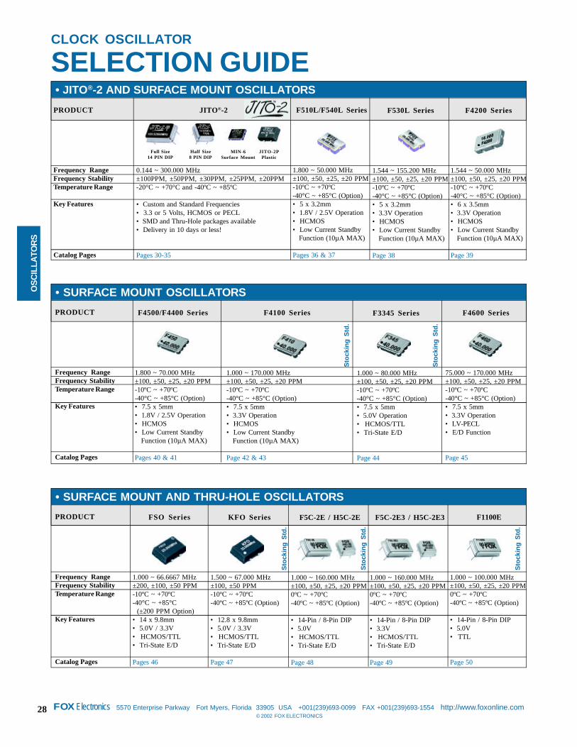
• SURFACE MOUNT AND THRU-HOLE OSCILLATORS
PRODUCT
Frequency RangeFrequency StabilityTemperature Range
Key Features
Catalog Pages
F5C-2E / H5C-2E
1.000 ~ 160.000 MHz±100, ±50, ±25, ±20 PPM0ºC ~ +70ºC-40ºC ~ +85ºC (Option)
• 14-Pin / 8-Pin DIP• 5.0V• HCMOS/TTL• Tri-State E/D
Page 48
KFO Series
1.500 ~ 67.000 MHz±100, ±50 PPM-10ºC ~ +70ºC-40ºC ~ +85ºC (Option)
• 12.8 x 9.8mm• 5.0V / 3.3V• HCMOS/TTL• Tri-State E/D
Page 47
FSO Series
1.000 ~ 66.6667 MHz±200, ±100, ±50 PPM-10ºC ~ +70ºC-40°C ~ +85°C (±200 PPM Option)• 14 x 9.8mm• 5.0V / 3.3V• HCMOS/TTL• Tri-State E/D
Pages 46
F5C-2E3 / H5C-2E3
1.000 ~ 160.000 MHz±100, ±50, ±25, ±20 PPM0ºC ~ +70ºC-40ºC ~ +85ºC (Option)
• 14-Pin / 8-Pin DIP• 3.3V• HCMOS/TTL• Tri-State E/D
Page 49
F1100E
1.000 ~ 100.000 MHz±100, ±50, ±25, ±20 PPM0ºC ~ +70ºC-40ºC ~ +85ºC (Option)
• 14-Pin / 8-Pin DIP• 5.0V• TTL
Page 50
Sto
ckin
g S
td.
Sto
ckin
g S
td.
Sto
ckin
g S
td.
• JITO®-2 AND SURFACE MOUNT OSCILLATORS
F530L Series
1.544 ~ 155.200 MHz±100, ±50, ±25, ±20 PPM-10ºC ~ +70ºC-40°C ~ +85°C (Option)• 5 x 3.2mm• 3.3V Operation• HCMOS• Low Current Standby Function (10µA MAX)
Page 38
JITO®-2
0.144 ~ 300.000 MHz±100PPM, ±50PPM, ±30PPM, ±25PPM, ±20PPM-20°C ~ +70°C and -40ºC ~ +85ºC
• Custom and Standard Frequencies• 3.3 or 5 Volts, HCMOS or PECL• SMD and Thru-Hole packages available• Delivery in 10 days or less!
Pages 30-35
F510L/F540L Series
1.800 ~ 50.000 MHz±100, ±50, ±25, ±20 PPM-10ºC ~ +70ºC-40°C ~ +85°C (Option)• 5 x 3.2mm• 1.8V / 2.5V Operation• HCMOS• Low Current Standby Function (10µA MAX)
Pages 36 & 37
Full Size14 PIN DIP
Half Size8 PIN DIP
MIN-6Surface Mount
JITO-2PPlastic
PRODUCT
Frequency RangeFrequency StabilityTemperature Range
Key Features
Catalog Pages
F4200 Series
1.544 ~ 50.000 MHz±100, ±50, ±25, ±20 PPM-10ºC ~ +70ºC-40°C ~ +85°C (Option)• 6 x 3.5mm• 3.3V Operation• HCMOS• Low Current Standby Function (10µA MAX)
Page 39
• SURFACE MOUNT OSCILLATORS
PRODUCT
Frequency RangeFrequency StabilityTemperature Range
Key Features
Catalog Pages
F3345 Series
1.000 ~ 80.000 MHz±100, ±50, ±25, ±20 PPM-10ºC ~ +70ºC-40°C ~ +85°C (Option)• 7.5 x 5mm• 5.0V Operation• HCMOS/TTL• Tri-State E/D
Page 44
F4100 Series
1.000 ~ 170.000 MHz±100, ±50, ±25, ±20 PPM-10ºC ~ +70ºC-40°C ~ +85°C (Option)• 7.5 x 5mm• 3.3V Operation• HCMOS• Low Current Standby Function (10µA MAX)
Page 42 & 43
F4500/F4400 Series
1.800 ~ 70.000 MHz±100, ±50, ±25, ±20 PPM-10ºC ~ +70ºC-40°C ~ +85°C (Option)• 7.5 x 5mm• 1.8V / 2.5V Operation• HCMOS• Low Current Standby Function (10µA MAX)
Pages 40 & 41
Sto
ckin
g S
td.
Sto
ckin
g S
td.
F4600 Series
75.000 ~ 170.000 MHz±100, ±50, ±25, ±20 PPM-10ºC ~ +70ºC-40°C ~ +85°C (Option)• 7.5 x 5mm• 3.3V Operation• LV-PECL• E/D Function
Page 45
OS
CIL
LATO
RS

29© 2002 FOX ELECTRONICS
FOXElectronics 5570 Enterprise Parkway Fort Myers, Florida 33905 USA +001(239)693-0099 FAX +001(239)693-1554 http://www.foxonline.com
CLOCK OSCILLATOR
GENERAL CHARACTERISTICS• MECHANICAL SPECIFICATIONSGross Leak TestHermetically Sealed PackageSeal Strength (Thru-Hole)Bend Test(Pin Material)Solvent Resistance
Marking InkSolderability
Maximum Soldering Temp.
All units 100% leak tested.Mass spectrometer leak rate less than 2 x 10 -8 Atm. CC/sec. of helium.2.27Kg max. force perpendicular to top and bottom.Will withstand maximum bend of 90°, referenced to base, for 2 bends.(Iron and Nickel - Nickel coated, solder dipped.)Isopropyl Alcohol, TrichloroethaneNote 1 - Ultrasonic cleaning not to be used.Note 2 - Unit can be cleaned in only one solvent listed.Epoxy, heat cured or UV cured (ceramic SMD)The terminals are considered solderable and acceptable for electrical connection if 95% of the cooled solder surfaceis uniform and free from breaks and pinholes. The other 5% of the cooled solder surface may show only pinholes,voids, or rough spots that are not concentrated in one area.270°C for 10 seconds on leads.
Reliability Tests: Shock, Vibration, Aging (Burn-in), Temperature Cycle.All specifications subject to change without notice. Rev. 05/03/00
OS
CILLA
TOR
S


1© 2002 FOX ELECTRONICS
FOXElectronics 5570 Enterprise Parkway Fort Myers, Florida 33905 USA +001(239)693-0099 FAX +001(239)693-1554 http://www.foxonline.com
OUTPUT (Pin 3)ACTIVEACTIVEHigh Z
• ENABLE / DISABLE FUNCTION 2
INH (Pin 1)OPEN 3
'1' Level VIH ≥ 2.31 V'0' Level VIL ≤ 0.99 V
All dimensions are in millimeters.
FEATURES• 3.3V Operation• HCMOS Output• Standby Function• Tape and Reel (2,000 pcs. STD)
3.3V HCMOS SMD OSCILLATOR WITH STANDBY
F330 SERIES
FrequencyStability1
±100PPM±100PPM±50PPM±50PPM±25PPM±20PPM
• MODEL NUMBER SELECTIONOperating
Temperature (ºC)-10 ~ +70-40 ~ +85-10 ~ +70-40 ~ +85-10 ~ +70-10 ~ +70
FrequencyRange (MHz)1.800 ~ 50.0001.800 ~ 50.0001.800 ~ 50.0001.800 ~ 50.0001.800 ~ 50.0001.800 ~ 50.000
F330F330RF335
F335RF336F338
Model Number
See page 53 for tape and reel specifications.
1.800 ~ 50.000 MHz-55ºC ~ +125ºC
3.3V ± 10%
20mA25mA
45% ~ 55%
6nS6nS
10% VDD
90% VDD Min2mA Min-2mA Min
15pF10µA5mS
150nS5mS
PARAMETERSFrequency Range (FO)Storage Temperature Range (TSTG)Supply Voltage (VDD)Input Current (IDD) 1.800 ~ 32.000 MHz 32.000+ ~ 50.000 MHz
Output Symmetry (50% VDD) 1.000 ~ 50.000 MHz
Rise Time (10% ~ 90% VDD) (TR)Fall Time (90% ~ 10% VDD) (TF)Output Voltage (VOL)
(VOH)Output Current (IOL)
(IOH)Output Load (HCMOS)Standby Current (VIL ≤ 0.99V)Start-up Time (TS)Output Disable Time 2
Output Enable Time 2
• ELECTRICAL CHARACTERISTICSMAX (unless otherwise noted)
1 Inclusive of 25ºC tolerance, operating temperature range, input voltage change, load change, aging, shock, and vibration.3 An internal pullup resistor from pin 1 to pin 4 allows active output if pin 1 is left open.See page 29 for mechanical specifications, test circuits, and output waveform.Note: A 0.01µF bypass capacitor should be placed between VDD (Pin 4) and GND (Pin 2) to minimize power supply line noise.All specifications subject to change without notice. Rev. 10/01/02

36 FOXElectronics 5570 Enterprise Parkway Fort Myers, Florida 33905 USA +001(239)693-0099 FAX +001(239)693-1554 http://www.foxonline.com© 2002 FOX ELECTRONICS
OS
CIL
LATO
RS
FEATURES• 1.8V Operation• HCMOS Output• Low Power Consumption• Standby Function• Tape and Reel (1,000 or 2,000 pcs. STD)
1.8V HCMOS CERAMIC SMD OSCILLATOR WITH STANDBY
F510L SERIES
FrequencyStability1
±100PPM±100PPM±50PPM±50PPM±25PPM±25PPM±20PPM
• MODEL NUMBER SELECTIONOperating
Temperature (ºC)-10 ~ +70-40 ~ +85-10 ~ +70-40 ~ +85-10 ~ +70-40 ~ +85-10 ~ +70
FrequencyRange (MHz)1.800 ~ 50.0001.800 ~ 50.0001.800 ~ 50.0001.800 ~ 50.0001.800 ~ 50.0001.800 ~ 50.0001.800 ~ 50.000
F510LF510LRF515L
F515LRF516L
F516LRF518L
Model Number
OUTPUT (Pin 3)ACTIVEACTIVEHigh Z
• ENABLE / DISABLE FUNCTION 2
INH (Pin 1)OPEN'1' Level VIH ≥ 0.7 V'0' Level VIL ≤ 0.3 V
See page 53 for tape and reel specifications.
All dimensions are in millimeters.
1 Inclusive of 25ºC tolerance, operating temperature range, input voltage change, load change,aging, shock, and vibration.See page 29 for mechanical specifications, test circuits, and output waveform.All specifications subject to change without notice. Rev. 05/01/02
1.800 ~ 50.000 MHz-55ºC ~ +125ºC
1.8V ± 5%
7mA15mA
40% ~ 60%
5nS3.5nS
5nS3.5nS
20% VDD
80% VDD Min2mA Min2mA Min
15pF10µA10mS300nS10mS
PARAMETERSFrequency Range (FO)Storage Temperature Range (TSTG)Supply Voltage (VDD)Input Current (IDD) 1.800 ~ 32.100 MHz 32.100+ ~ 50.000 MHzOutput Symmetry (50% VDD)Rise Time (20% ~ 80% VDD) (TR) 1.800 ~ 32.100 MHz 32.100+ ~ 50.000 MHzFall Time (80% ~ 20% VDD) (TF) 1.800 ~ 32.100 MHz 32.100+ ~ 50.000 MHzOutput Voltage (VOL)
(VOH)Output Current (IOL)
(IOH)Output Load (HCMOS)Standby CurrentStart-up Time (TS)Output Disable Time 2
Output Enable Time 2
• ELECTRICAL CHARACTERISTICSMAX (unless otherwise noted)

37© 2002 FOX ELECTRONICS
FOXElectronics 5570 Enterprise Parkway Fort Myers, Florida 33905 USA +001(239)693-0099 FAX +001(239)693-1554 http://www.foxonline.com
OS
CILLA
TOR
S
FEATURES• 2.5V Operation• HCMOS Output• Low Power Consumption• Standby Function• Tape and Reel (1,000 or 2,000 pcs. STD)
2.5V HCMOS CERAMIC SMD OSCILLATOR WITH STANDBY
F540L SERIES
FrequencyStability1
±100PPM±100PPM±50PPM±50PPM±25PPM±25PPM±20PPM
• MODEL NUMBER SELECTIONOperating
Temperature (ºC)-10 ~ +70-40 ~ +85-10 ~ +70-40 ~ +85-10 ~ +70-40 ~ +85-10 ~ +70
FrequencyRange (MHz)1.800 ~ 50.0001.800 ~ 50.0001.800 ~ 50.0001.800 ~ 50.0001.800 ~ 50.0001.800 ~ 50.0001.800 ~ 50.000
F540LF540LRF545L
F545LRF546L
F546LRF548L
Model Number
OUTPUT (Pin 3)ACTIVEACTIVEHigh Z
• ENABLE / DISABLE FUNCTION 2
INH (Pin 1)OPEN'1' Level VIH ≥ 0.7 V'0' Level VIL ≤ 0.3 V
See page 53 for tape and reel specifications.
All dimensions are in millimeters.
1 Inclusive of 25ºC tolerance, operating temperature range, input voltage change, load change,aging, shock, and vibration.See page 29 for mechanical specifications, test circuits, and output waveform.All specifications subject to change without notice. Rev. 05/01/02
1.800 ~ 50.000 MHz-55ºC ~ +125ºC
2.5V ± 5%
10mA12mA
45% ~ 55%5nS5nS
10% VDD
90% VDD Min4mA Min4mA Min
15pF10µA10mS150nS10mS
PARAMETERSFrequency Range (FO)Storage Temperature Range (TSTG)Supply Voltage (VDD)Input Current (IDD) 1.800 ~ 32.100 MHz 32.100+ ~ 50.000 MHzOutput Symmetry (50% VDD)Rise Time (10% ~ 90% VDD) (TR)Fall Time (90% ~ 10% VDD) (TF)Output Voltage (VOL)
(VOH)Output Current (IOL)
(IOH)Output Load (HCMOS)Standby CurrentStart-up Time (TS)Output Disable Time 2
Output Enable Time 2
• ELECTRICAL CHARACTERISTICSMAX (unless otherwise noted)

38 FOXElectronics 5570 Enterprise Parkway Fort Myers, Florida 33905 USA +001(239)693-0099 FAX +001(239)693-1554 http://www.foxonline.com© 2002 FOX ELECTRONICS
OS
CIL
LATO
RS
FEATURES• 3.3V Operation• HCMOS Output• Standby Function• Tape and Reel (1,000 or 2,000 pcs. STD)
3.3V HCMOS CERAMIC SMD OSCILLATOR WITH STANDBY
F530L SERIES
FrequencyStability1
±100PPM±100PPM±50PPM±50PPM±25PPM±25PPM±20PPM
• MODEL NUMBER SELECTIONOperating
Temperature (ºC)-10 ~ +70-40 ~ +85-10 ~ +70-40 ~ +85-10 ~ +70-40 ~ +85-10 ~ +70
FrequencyRange (MHz)
1.544 ~ 155.5201.544 ~ 155.5201.544 ~ 155.5201.544 ~ 155.5201.544 ~ 155.5201.544 ~ 50.0001.544 ~ 50.000
F530LF530LRF535L
F535LRF536L
F536LRF538L
Model Number
OUTPUT (Pin 3)ACTIVEACTIVEHigh Z
• ENABLE / DISABLE FUNCTION 2
INH (Pin 1)OPEN'1' Level VIH ≥ 2.31 V'0' Level VIL ≤ 0.99 V
See page 53 for tape and reel specifications.
OPTIONS• 5.0V (F550L) VersionAvailable
All dimensions are in millimeters.
1.544 ~ 155.520 MHz-40ºC ~ +85ºC
3.3V ± 10%20mA
40% ~ 60%7nS7nS
10% VDD
90% VDD Min2mA Min-2mA Min
15pF10µA10mS150nS10mS
PARAMETERSFrequency Range (FO)Storage Temperature Range (TSTG)Supply Voltage (VDD)Input Current (IDD)Output Symmetry (50% VDD)Rise Time (10% ~ 90% VDD) (TR)Fall Time (90% ~ 10% VDD) (TF)Output Voltage (VOL)
(VOH)Output Current (IOL)
(IOH)Output Load HCMOSStandby CurrentStart-up Time (TS)Output Disable Time 2
Output Enable Time 2
• ELECTRICAL CHARACTERISTICSMAX (unless otherwise noted)
1 Inclusive of 25ºC tolerance, operating temperature range, input voltage change, load change,aging, shock, and vibration.See page 29 for mechanical specifications, test circuits, and output waveform.All specifications subject to change without notice. Rev. 05/01/02

39© 2002 FOX ELECTRONICS
FOXElectronics 5570 Enterprise Parkway Fort Myers, Florida 33905 USA +001(239)693-0099 FAX +001(239)693-1554 http://www.foxonline.com
OS
CILLA
TOR
S
FEATURES• 3.3V Operation• HCMOS Output• Standby Function• Tape and Reel (2,000 pcs. STD)
3.3V HCMOS CERAMIC SMD OSCILLATOR WITH STANDBY
F4200 SERIES
OUTPUT (Pin 3)ACTIVEACTIVEHigh Z
• ENABLE / DISABLE FUNCTION 2
INH (Pin 1)OPEN 3'1' Level VIH ≥ 2.31 V'0' Level VIL ≤ 0.99 V
FrequencyStability1
±100PPM±100PPM±50PPM±50PPM±25PPM±25PPM±20PPM
• MODEL NUMBER SELECTIONOperating
Temperature (ºC)-10 ~ +70-40 ~ +85-10 ~ +70-40 ~ +85-10 ~ +70-40 ~ +85-10 ~ +70
FrequencyRange (MHz)1.544 ~ 50.0001.544 ~ 50.0001.544 ~ 50.0001.544 ~ 50.0001.544 ~ 50.0001.544 ~ 50.0001.544 ~ 50.000
F4200F4200RF4205
F4205RF4206
F4206RF4208
Model Number
See page 53 for tape and reel specifications.
All dimensions are in millimeters.
OPTIONS• 5.0V (F3400) Version Available
1 Inclusive of 25ºC tolerance, operating temperature range, input voltage change, load change,aging, shock, and vibration.3 An internal pullup resistor from pin 1 to pin 4 allows active output if pin 1 is left open.See page 29 for mechanical specifications, test circuits, and output waveform.All specifications subject to change without notice. Rev. 05/01/02
1.544 ~ 50.000 MHz-40ºC ~ +85ºC
3.3V ± 10%20mA
40% ~ 60%6nS6nS
10% VDD
90% VDD Min2mA Min-2mA Min
15pF10µA10mS150nS10nS
PARAMETERSFrequency Range (FO)Storage Temperature Range (TSTG)Supply Voltage (VDD)Input Current (IDD)Output Symmetry (50% VDD)Rise Time (10% ~ 90% VDD) (TR)Fall Time (90% ~ 10% VDD) (TF)Output Voltage (VOL)
(VOH)Output Current (IOL)
(IOH)Output Load (HCMOS)Standby CurrentStart-up Time (TS)Output Disable Time 2
Output Enable Time 2
• ELECTRICAL CHARACTERISTICSMAX (unless otherwise noted)

40 FOXElectronics 5570 Enterprise Parkway Fort Myers, Florida 33905 USA +001(239)693-0099 FAX +001(239)693-1554 http://www.foxonline.com© 2002 FOX ELECTRONICS
OS
CIL
LATO
RS
FEATURES• 1.8V Operation• HCMOS Output• Low Power Consumption• Standby Function• Tape and Reel (2,000 pcs. STD)
1.8V HCMOS SMD OSCILLATOR WITH STANDBY
F4500 SERIES
FrequencyStability1
±100PPM±100PPM±50PPM±50PPM±25PPM±25PPM±20PPM
• MODEL NUMBER SELECTIONOperating
Temperature (ºC)-10 ~ +70-40 ~ +85-10 ~ +70-40 ~ +85-10 ~ +70-40 ~ +85-10 ~ +70
FrequencyRange (MHz)1.800 ~ 70.0001.800 ~ 70.0001.800 ~ 70.0001.800 ~ 70.0001.800 ~ 70.0001.800 ~ 70.0001.800 ~ 70.000
F4500F4500RF4505
F4505RF4506
F4506RF4508
Model Number
OUTPUT (Pin 3)ACTIVEACTIVEHigh Z
• ENABLE / DISABLE FUNCTION 2
INH (Pin 1)OPEN 3'1' Level VIH ≥ 0.7 V'0' Level VIL ≤ 0.3 V
See page 53 for tape and reel specifications.
1 Inclusive of 25ºC tolerance, operating temperature range, input voltage change, load change,aging, shock, and vibration.3 An internal pullup resistor from pin 1 to pin 4 allows active output if pin 1 is left open.See page 29 for mechanical specifications, test circuits, and output waveform.Note: A 0.01µF bypass capacitor should be placed between VDD (Pin 4) and GND (Pin 2) to minimize power supply line noise.All specifications subject to change without notice. Rev. 05/01/02
1.800 ~ 70.000 MHz-55ºC ~ +125ºC
1.8V ± 5%
7mA15mA
40% ~ 60%
5nS3.5nS
5nS3.5nS
20% VDD
80% VDD Min2mA Min2mA Min
15pF10µA10mS300nS10mS
PARAMETERSFrequency Range (FO)Storage Temperature Range (TSTG)Supply Voltage (VDD)Input Current (IDD) 1.000 ~ 32.100 MHz 32.100+ ~ 70.000 MHzOutput Symmetry (50% VDD)Rise Time (20% ~ 80% VDD) (TR) 1.800 ~ 32.100 MHz 32.100+ ~ 70.000 MHzFall Time (80% ~ 20% VDD) (TF) 1.800 ~ 32.100 MHz 32.100+ ~ 70.000 MHzOutput Voltage (VOL)
(VOH)Output Current (IOL)
(IOH)Output Load (HCMOS)Standby CurrentStart-up Time (TS)Output Disable Time 2
Output Enable Time 2
• ELECTRICAL CHARACTERISTICSMAX (unless otherwise noted)
All dimensions are in millimeters.

41© 2002 FOX ELECTRONICS
FOXElectronics 5570 Enterprise Parkway Fort Myers, Florida 33905 USA +001(239)693-0099 FAX +001(239)693-1554 http://www.foxonline.com
OS
CILLA
TOR
S
See page 53 for tape and reel specifications.
2.5V HCMOS SMD OSCILLATOR WITH STANDBY
F4400 SERIESFEATURES• 2.5V Operation• HCMOS Output• Low Power Consumption• Standby Function• Tape and Reel (2,000 pcs. STD)
OUTPUT (Pin 3)
ACTIVEHigh Z
• ENABLE / DISABLE FUNCTION 2
INH (Pin 1)OPEN 3'1' Level VIH ≥ 0.7 V'0' Level VIL ≤ 0.3 V
1 Inclusive of 25ºC tolerance, operating temperature range, input voltage change, load change,aging, shock, and vibration.3 Pin #1: In case of open connection, oscillator is not functioning.See page 29 for mechanical specifications, test circuits, and output waveform.Note: A 0.01µF bypass capacitor should be placed between VDD (Pin 4) and GND (Pin 2) to minimize power supply line noise.All specifications subject to change without notice. Rev. 05/01/02
FrequencyStability1
±100PPM±100PPM±50PPM±50PPM±25PPM±25PPM±20PPM
• MODEL NUMBER SELECTIONOperating
Temperature (ºC)-10 ~ +70-40 ~ +85-10 ~ +70-40 ~ +85-10 ~ +70-40 ~ +85-10 ~ +70
FrequencyRange (MHz)1.800 ~ 50.0001.800 ~ 50.0001.800 ~ 50.0001.800 ~ 50.0001.800 ~ 50.0001.800 ~ 50.0001.800 ~ 50.000
F4400F4400RF4405
F4405RF4406
F4406RF4408
Model Number
1.800 ~ 50.000 MHz-55ºC ~ +125ºC
2.5V ± 5%
10mA12mA
45% ~ 55%5nS5nS
10% VDD
90% VDD Min4mA Min4mA Min
15pF10µA10mS150nS10mS
PARAMETERSFrequency Range (FO)Storage Temperature Range (TSTG)Supply Voltage (VDD)Input Current (IDD) 1.800 ~ 32.100 MHz 32.100+ ~ 50.000 MHzOutput Symmetry (50% VDD)Rise Time (10% ~ 90% VDD) (TR)Fall Time (90% ~ 10% VDD) (TF)Output Voltage (VOL)
(VOH)Output Current (IOL)
(IOH)Output Load (HCMOS)Standby CurrentStart-up Time (TS)Output Disable Time 2
Output Enable Time 2
• ELECTRICAL CHARACTERISTICSMAX (unless otherwise noted)
All dimensions are in millimeters.

2 FOXElectronics 5570 Enterprise Parkway Fort Myers, Florida 33905 USA +001(239)693-0099 FAX +001(239)693-1554 http://www.foxonline.com© 2002 FOX ELECTRONICS
OUTPUT (Pin 3)ACTIVEACTIVEHigh Z
• ENABLE / DISABLE FUNCTION 2
INH (Pin 1)OPEN 2
'1' Level VIH ≥ 70% VDD
'0' Level VIL ≤ 30% VDD
All dimensions are in millimeters.
FEATURES• 2.85V Operation• HCMOS Output• Standby Function• Tape and Reel (2,000 pcs. STD)
2.85V HCMOS SMD OSCILLATOR WITH STANDBY
F4300 SERIES
See page 53 for tape and reel specifications.
FrequencyStability±100PPM±50PPM±25PPM±20PPM
• MODEL NUMBER SELECTIONOperating
Temperature (ºC)-10 ~ +70-10 ~ +70-10 ~ +70-10 ~ +70
FrequencyRange (MHz)1.544 ~ 80.0001.544 ~ 80.0001.544 ~ 80.0001.544 ~ 80.000
F4300F4305F4306F4308
Model Number
1.544 ~ 80.000 MHz-55ºC ~ +125ºC
2.85V ± 5%
15mA20mA25mA30mA
45% ~ 55%
6nS4nS
6nS4nS
10% VDD
90% VDD Min2mA-2mA15pF10µA10mS150nS10mS
PARAMETERSFrequency Range (FO)Temperature Range (TSTG)Supply Voltage (VDD)Input Current (IDD) 1.544 ~ 32.000 MHz 32.000+ ~ 50.000 MHz 50.000+ ~ 67.000 MHz 67.000+ ~ 80.000 MHzOutput Symmetry (50% VDD)Rise Time (10% ~ 90% VDD) (TR) 1.544 ~ 50.000 MHz 50.000 ~ 80.000 MHzFall Time (90% ~ 10% VDD) (TF) 1.544 ~ 50.000 MHz 50.000 ~ 80.000 MHzOutput Voltage (IOL = 2mA) (VOL)
(IOH = 2mA) (VOH)Output Current (VOL = 10% VDD) (IOL)
(VOH = 90% VDD) (IOH)Output Load (HCMOS)Standby Current (VIL ≤ 30%VDD)Start-up Time (TS)Output Disable Time 2
Output Enable Time 2
• ELECTRICAL CHARACTERISTICSMAX (unless otherwise noted)
1 Inclusive of 25ºC tolerance, operating temperature range, input voltage change, load change, aging, shock, and vibration.2 An internal pullup resistor from pin 1 to pin 4 allows active output if pin 1 is left open.See page 29 for mechanical specifications, test circuits, and output waveform.Note: A 0.01µF bypass capacitor should be placed between VDD (Pin 4) and GND (Pin 2) to minimize power supply line noise.All specifications subject to change without notice. Rev. 11/11/02

42 FOXElectronics 5570 Enterprise Parkway Fort Myers, Florida 33905 USA +001(239)693-0099 FAX +001(239)693-1554 http://www.foxonline.com© 2002 FOX ELECTRONICS
OS
CIL
LATO
RS
OUTPUT (Pin 3)ACTIVEACTIVEHigh Z
• ENABLE / DISABLE FUNCTION 2
INH (Pin 1)OPEN 3'1' Level VIH ≥ 2.31 V'0' Level VIL ≤ 0.99 V
All dimensions are in millimeters.
FEATURES• 3.3V Operation• HCMOS Output• Standby Function• Tape and Reel (2,000 pcs. STD)
3.3V HCMOS SMD OSCILLATOR WITH STANDBY
F4100 SERIES
FrequencyStability1
±100PPM±100PPM±50PPM±50PPM±25PPM±25PPM±20PPM
• MODEL NUMBER SELECTIONOperating
Temperature (ºC)-10 ~ +70-40 ~ +85-10 ~ +70-40 ~ +85-10 ~ +70-40 ~ +85-10 ~ +70
FrequencyRange (MHz)
1.000 ~ 170.0001.000 ~ 170.0001.000 ~ 170.0001.000 ~ 170.0001.000 ~ 125.0001.000 ~ 100.0001.000 ~ 80.000
F4100F4100RF4105
F4105RF4106
F4106RF4108
Model Number
See page 53 for tape and reel specifications.
1.000 ~ 170.000 MHz-55ºC ~ +125ºC
3.3V ± 10%
15mA20mA25mA40mA
45% ~ 55%40% ~ 60%
6nS6nS
10% VDD
90% VDD Min2mA Min-2mA Min
15pF10µA10mS150nS10mS
PARAMETERSFrequency Range (FO)Storage Temperature Range (TSTG)Supply Voltage (VDD)Input Current (IDD) 1.000 ~ 32.000 MHz 32.000+ ~ 50.000 MHz 50.000+ ~ 67.000 MHz 67.000+ ~ 170.000 MHzOutput Symmetry (50% VDD) 1.000 ~ 50.000 MHz 50.000+ ~ 170.000 MHzRise Time (10% ~ 90% VDD) (TR)Fall Time (90% ~ 10% VDD) (TF)Output Voltage (VOL)
(VOH)Output Current (IOL)
(IOH)Output Load (HCMOS)Standby Current (VIL ≤ 0.99V)Start-up Time (TS)Output Disable Time 2
Output Enable Time 2
• ELECTRICAL CHARACTERISTICSMAX (unless otherwise noted)
OPTIONS• 1.05mm Height Max
1 Inclusive of 25ºC tolerance, operating temperature range, input voltage change, load change,aging, shock, and vibration.3 An internal pullup resistor from pin 1 to pin 4 allows active output if pin 1 is left open.See page 29 for mechanical specifications, test circuits, and output waveform.Note: A 0.01µF bypass capacitor should be placed between VDD (Pin 4) and GND (Pin 2) to minimize power supply line noise.All specifications subject to change without notice. Rev. 05/01/02
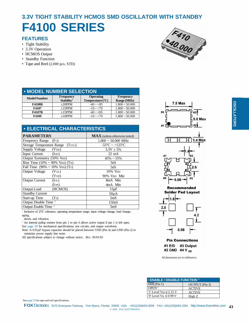
43© 2002 FOX ELECTRONICS
FOXElectronics 5570 Enterprise Parkway Fort Myers, Florida 33905 USA +001(239)693-0099 FAX +001(239)693-1554 http://www.foxonline.com
OS
CILLA
TOR
S
OUTPUT (Pin 3)ACTIVEACTIVEHigh Z
• ENABLE / DISABLE FUNCTION 2
INH (Pin 1)OPEN 3'1' Level VIH ≥ 2.31 V'0' Level VIL ≤ 0.99 V
All dimensions are in millimeters.
FEATURES• Tight Stability• 3.3V Operation• HCMOS Output• Standby Function• Tape and Reel (2,000 pcs. STD)
3.3V TIGHT STABILITY HCMOS SMD OSCILLATOR WITH STANDBY
F4100 SERIES
FrequencyStability1
±20PPM±15PPM±15PPM±10PPM
• MODEL NUMBER SELECTIONOperating
Temperature (ºC)-40 ~ +85-10 ~ +70-40 ~ +85-10 ~ +70
FrequencyRange (MHz)1.800 ~ 50.0001.800 ~ 50.0001.800 ~ 50.0001.800 ~ 50.000
F4108RF4107
F4107RF4109
Model Number
See page 53 for tape and reel specifications.
1 Inclusive of 25ºC tolerance, operating temperature range, input voltage change, load change,aging, shock, and vibration.3 An internal pullup resistor from pin 1 to pin 4 allows active output if pin 1 is left open.See page 29 for mechanical specifications, test circuits, and output waveform.Note: A 0.01µF bypass capacitor should be placed between VDD (Pin 4) and GND (Pin 2) to minimize power supply line noise.All specifications subject to change without notice. Rev. 05/01/02
1.800 ~ 50.000 MHz-55ºC ~ +125ºC
3.3V ± 5%22 mA
45% ~ 55%5nS5nS
10% VDD
90% VDD Min8mA Min4mA Min
15pF50µA5mS
150nS5mS
PARAMETERSFrequency Range (FO)Storage Temperature Range (TSTG)Supply Voltage (VDD)Input Current (IDD)Output Symmetry (50% VDD)Rise Time (10% ~ 90% VDD) (TR)Fall Time (90% ~ 10% VDD) (TF)Output Voltage (VOL)
(VOH)Output Current (IOL)
(IOH)Output Load (HCMOS)Standby CurrentStart-up Time (TS)Output Disable Time 2
Output Enable Time 2
• ELECTRICAL CHARACTERISTICSMAX (unless otherwise noted)

44 FOXElectronics 5570 Enterprise Parkway Fort Myers, Florida 33905 USA +001(239)693-0099 FAX +001(239)693-1554 http://www.foxonline.com© 2002 FOX ELECTRONICS
OS
CIL
LATO
RS
FEATURES• 5.0V Operation• HCMOS/TTL Output• Tri-State Enable/Disable• Tape and Reel (2,000 pcs. STD)
See page 53 for tape and reel specifications.
5.0V HCMOS SMD OSCILLATOR
F3345 SERIES
FrequencyStability1
±100PPM±100PPM±50PPM±50PPM±25PPM±25PPM±20PPM
• MODEL NUMBER SELECTIONOperating
Temperature (ºC)-10 ~ +70-40 ~ +85-10 ~ +70-40 ~ +85-10 ~ +70-40 ~ +85-10 ~ +70
FrequencyRange (MHz)1.000 ~ 80.0001.000 ~ 80.0001.000 ~ 80.0001.000 ~ 80.0001.000 ~ 80.0001.000 ~ 80.0001.000 ~ 80.000
F3345F3345RF3340
F3340RF3346
F3346RF3348
Model Number
All dimensions are in millimeters.
1 Inclusive of 25ºC tolerance, operating temperature range, input voltage change, load change,aging, shock, and vibration.3 An internal pullup resistor from pin 1 to pin 4 allows active output if pin 1 is left open.See page 29 for mechanical specifications, test circuits, and output waveform.Note: A 0.01µF bypass capacitor should be placed between VDD (Pin 4) and GND (Pin 2) to minimize power supply line noise.All specifications subject to change without notice. Rev. 05/01/02
1.000 ~ 80.000 MHz-55ºC ~ +125ºC
5.0V ± 10%
25mA40mA60mA73mA
45% ~ 55%5nS5nS
10% VDD
90% VDD Min16mA Min-16mA Min
10TTL50pF10mS100nS
PARAMETERSFrequency Range (FO)Storage Temperature Range (TSTG)Supply Voltage (VDD)Input Current (IDD) 1.000 ~ 25.000 MHz 25.000+ ~ 50.000 MHz 50.000+ ~ 67.000 MHz 67.000+ ~ 80.000 MHzOutput Symmetry (50% VDD)Rise Time (10% ~ 90% VDD) (TR)Fall Time (90% ~ 10% VDD) (TF)Output Voltage (VOL)
(VOH)Output Current (IOL)
(IOH)Output Load TTL HCMOSStart-up Time (TS)Enable/Disable Time 2
• ELECTRICAL CHARACTERISTICS
OUTPUT (Pin 3)ACTIVEACTIVEHigh Z
• ENABLE / DISABLE FUNCTION 2
INH (Pin 1)OPEN 3'1' Level VIH ≥ 2.2 V'0' Level VIL ≤ 0.8 V
MAX (unless otherwise noted)
OPTIONS• 1.05mm Height Max• Standby Function (F4101)

45© 2002 FOX ELECTRONICS
FOXElectronics 5570 Enterprise Parkway Fort Myers, Florida 33905 USA +001(239)693-0099 FAX +001(239)693-1554 http://www.foxonline.com
OS
CILLA
TOR
S3.3V LV-PECL OSCILLATOR WITH STANDBY
F4600 SERIES
FrequencyStability1
±100PPM±100PPM±50PPM±50PPM±25PPM±25PPM±20PPM
• MODEL NUMBER SELECTIONOperating
Temperature (ºC)-10 ~ +70-40 ~ +85-10 ~ +70-40 ~ +85-10 ~ +70-40 ~ +85-10 ~ +70
FrequencyRange (MHz)
75.000 ~ 170.00075.000 ~ 170.00075.000 ~ 170.00075.000 ~ 170.00075.000 ~ 170.00075.000 ~ 170.00075.000 ~ 170.000
F4600F4600RF4605
F4605RF4606
F4606RF4608
Model Number
75.000 ~ 170.000 MHz-55ºC ~ +125ºC
3.3V ± 5%60mA
40% ~ 60%1nS1nS1.7V
2.2V Min5 Gates10µA10mS100nS10mS
PARAMETERSFrequency Range (FO)Storage Temperature Range (TSTG)Supply Voltage (VDD)Input Current (IDD)Output Symmetry (50% Vp-p Level)Rise Time (20% ~ 80% Vp-p) (TR)Fall Time (80% ~ 20% Vp-p) (TF)Output Voltage (VOL)
(VOH)Output LoadStandby CurrentStart-up Time (TS)Output Disable Time 2
Output Enable Time 2
• ELECTRICAL CHARACTERISTICS
1 Inclusive of 25ºC tolerance, operating temperature range, input voltage change, load change,aging, shock, and vibration.See page 29 for mechanical specifications, test circuits, and output waveform.Note: A 0.01µF bypass capacitor should be placed between VDD (Pin 6) and GND (Pin 3) to minimize power supply line noise.All specifications subject to change without notice. Rev. 05/01/02
FEATURES• 3.3V Operation• LV-PECL Output• Complementary Outputs• Standby Function• Tape and Reel (2,000 pcs. STD)
OUTPUT (Pin 4)ACTIVEACTIVEHigh Z
• ENABLE / DISABLE FUNCTION 2
INH (Pin 1)OPEN'1' Level VIH ≥ 0.7 V'0' Level VIL ≤ 0.3 V
All dimensions are in millimeters.
OUTPUT (Pin 5)ACTIVEACTIVEHigh Z
See page 53 for tape and reel specifications.
MAX (unless otherwise noted)

46 FOXElectronics 5570 Enterprise Parkway Fort Myers, Florida 33905 USA +001(239)693-0099 FAX +001(239)693-1554 http://www.foxonline.com© 2002 FOX ELECTRONICS
1 Inclusive of 25ºC tolerance, operating temperature range, input voltage change, and load change.3 An internal pullup resistor from pin 1 to pin 4 allows active output if pin 1 is left open.4 The FSO-2 and FSO-3 models will also operate over -40ºC ~ +85ºC, but with a relax stability of ±200 PPM.See page 29 for mechanical specifications, test circuits, and output waveform.Note: A 0.01µF bypass capacitor should be placed between VDD (Pin 4) and GND (Pin 2) to minimize power supply line noise.All specifications subject to change without notice. Rev. 05/01/02
FrequencyStability1
±100PPM±100PPM±50PPM±100PPM±100PPM±50PPM
• MODEL NUMBER SELECTIONOperating
Temperature (ºC)-20 ~ +70-40 ~ +85-20 ~ +70-20 ~ +70-40 ~ +85-20 ~ +70
FrequencyRange (MHz)
1.000 ~ 66.66671.000 ~ 66.66671.000 ~ 66.66671.000 ~ 66.66671.000 ~ 66.66671.000 ~ 66.6667
FSO-2 4
FSO-2RFSO-25FSO-3 4
FSO-3RFSO-35
ModelNumber
5.0 ± 0.5
3.3 ± 0.3
VDD (V)
5.0V/3.3V PLASTIC HCMOS SMD CLOCK OSCILLATOR
FEATURES• 5.0V / 3.3V Operation• HCMOS/TTL Output• Tri-State Enable/Disable• Extended Temperature Range• Tape and Reel (1,000 pcs. STD)
FSO SERIES
OUTPUT (Pin 3)ACTIVEACTIVEHigh Z
• ENABLE / DISABLE FUNCTION 2
INH (Pin 1)OPEN 3'1' Level VIH ≥ 2.4 V'0' Level VIL ≤ 0.6 V
1.000 ~ 66.6667 MHzPARAMETERSFrequency Range (FO)Input Current (IDD) 1.000 ~ 30.000 MHz 30.000+ ~ 66.6667 MHzOutput Symmetry (50% VDD)Rise Time (20% ~ 80% VDD) (TR) 1.000 ~ 30.000 MHz 30.000+ ~ 66.6667 MHzFall Time (80% ~ 20% VDD) (TF) 1.000 ~ 30.000 MHz 30.000+ ~ 66.6667 MHzOutput Voltage (VOL)
(VOH)Output Current (IOL)
(IOH)Output Load (TTL)
(HCMOS)Start-up Time (TS) 1.000 ~ 30.000 MHz 30.000+ ~ 66.6667 MHzEnable/Disable Time 2
• ELECTRICAL CHARACTERISTICSFSO-2 Series FSO-3 Series
23mA35mA
9mA20mA
40% ~ 60%
8nS7nS
8nS7nS0.4V
4.6V Min16mA Min-16mA Min
10TTL50pF
6nS6nS
6nS6nS0.4V
2.9V Min4mA Min-4mA Min
---30pF
4mS10mS100nS
See page 53 for tape and reel specifications.
All dimensions are in millimeters.
MAX (unless otherwise noted)
OS
CIL
LATO
RS

47© 2002 FOX ELECTRONICS
FOXElectronics 5570 Enterprise Parkway Fort Myers, Florida 33905 USA +001(239)693-0099 FAX +001(239)693-1554 http://www.foxonline.com
OS
CIL
LATO
RS
OUTPUT (Pin 3)ACTIVEACTIVEHigh Z
• ENABLE / DISABLE FUNCTION 2
INH (Pin 1)OPEN 3'1' Level VIH ≥ 2.2 V'0' Level VIL ≤ 0.8 V
All dimensions are in millimeters.
FEATURES• 5.0V Operation• HCMOS/TTL Output• Tri-State Enable/Disable• Tape and Reel (1,000 pcs. STD)
5.0V PLASTIC HCMOS/TTL SMD OSCILLATOR
KFO SERIES
See page 53 for tape and reel specifications.
1 Inclusive of 25ºC tolerance, operating temperature range, input voltage change, load change,aging, shock, and vibration.3 An internal pullup resistor from pin 1 to pin 4 allows active output if pin 1 is left open.See page 29 for mechanical specifications, test circuits, and output waveform.Note: A 0.01µF bypass capacitor should be placed between VDD (Pin 4) and GND (Pin 2) to minimize power supply line noise.All specifications subject to change without notice. Rev. 05/01/02
FrequencyStability1
±100PPM±100PPM±50PPM
• MODEL NUMBER SELECTIONOperating
Temperature (ºC)-10 ~ +70-40 ~ +85-10 ~ +70
FrequencyRange (MHz)1.500 ~ 67.0001.500 ~ 67.0001.500 ~ 67.000
KFO90ATKFO90FTKFO95AT
Model Number
1.500 ~ 67.000 MHz-55ºC ~ +125ºC
5.0V ± 10%
27mA45mA60mA
45% ~ 55%40% ~ 60%
7nS7nS
10% VDD
90% VDD Min16mA Min-16mA Min
10TTL50pF10mS100nS
PARAMETERSFrequency Range (FO)Storage Temperature Range (TSTG)Supply Voltage (VDD)Input Current (IDD) 1.500 ~ 32.000 MHz 32.000+ ~ 50.000 MHz 50.000+ ~ 67.000 MHzOutput Symmetry (50% VDD) 1.500 ~ 50.000 MHz 50.000+ ~ 67.000 MHzRise Time (10% ~ 90% VDD) (TR)Fall Time (90% ~ 10% VDD) (TF)Output Voltage (VOL)
(VOH)Output Current (IOL)
(IOH)Output Load TTL HCMOSStart-up Time (TS)Enable/Disable Time 2
• ELECTRICAL CHARACTERISTICSMAX (unless otherwise noted)
OPTIONS• 3.3V Operation (KFO30AT)
OS
CILLA
TOR
S

48 FOXElectronics 5570 Enterprise Parkway Fort Myers, Florida 33905 USA +001(239)693-0099 FAX +001(239)693-1554 http://www.foxonline.com© 2002 FOX ELECTRONICS
OS
CIL
LATO
RS
FEATURES• 3.3V Operation• HCMOS Output• Tri-State Enable/Disable• 14-Pin DIP / 8-Pin DIP
3.3V TRI-STATE ENABLE/DISABLE OSCILLATORS
F5C-2E3 / H5C-2E3
OUTPUT (Pin 8)ACTIVEACTIVEHigh Z
• ENABLE / DISABLE FUNCTION 2
INH (Pin 1)OPEN 3'1' Level VIH ≥ 2.2 V'0' Level VIL ≤ 0.8 V
1 Inclusive of 25ºC tolerance, operating temperature range, input voltage change, load change,aging, shock, and vibration.3 An internal pullup resistor from pin 1 to pin 14 allows active output if pin 1 is left open.See page 29 for mechanical specifications, test circuits, and output waveform.All specifications subject to change without notice. Rev. 05/01/02
FrequencyStability1
±100PPM±100PPM±50PPM±50PPM±25PPM±25PPM±20PPM
• MODEL NUMBER SELECTIONOperating
Temperature (ºC)0 ~ +70
-40 ~ +850 ~ +70
-40 ~ +850 ~ +70
-40 ~ +850 ~ +70
FrequencyRange (MHz)
1.000 ~ 160.0001.000 ~ 160.0001.000 ~ 160.0001.000 ~ 160.0001.000 ~ 160.0001.000 ~ 160.0001.000 ~ 160.000
F5C-2E3F5C-2E3RF6C-2E3F6C-2E3RF7C-2E3F7C-2E3RF8C-2E3
Model Number
H5C-2E3H5C-2E3RH6C-2E3H6C-2E3RH7C-E3H7C-2E3RH8C-2E3
///////
All dimensions are in millimeters.
F5C-2E3 H5C-2E3
1.000 ~ 160.000 MHz-55ºC ~ +125ºC
3.3V ± 10%
20mA40mA
40% ~ 60%10 nS10 nS
10% VDD
90% VDD Min8mA Min-8mA Min
15pF10mS100nS
PARAMETERSFrequency Range (FO)Storage Temperature Range (TSTG)Supply Voltage (VDD)Input Current (IDD) 1.000 ~ 40.000 MHz 40.000+ ~ 160.000 MHzOutput Symmetry (50% VDD)Rise Time (10% ~ 90% VDD) (TR)Fall Time (90% ~ 10% VDD) (TF)Output Voltage (VOL)
(VOH)Output Current (IOL)
(IOH)Output Load (HCMOS)Start-up Time (TS)Output Enable/Disable Time 2
• ELECTRICAL CHARACTERISTICSMAX (unless otherwise noted)

49© 2002 FOX ELECTRONICS
FOXElectronics 5570 Enterprise Parkway Fort Myers, Florida 33905 USA +001(239)693-0099 FAX +001(239)693-1554 http://www.foxonline.com
OS
CILLA
TOR
S
All dimensions are in millimeters.
F5C-2E H5C-2E
OUTPUT (Pin 8)ACTIVEACTIVEHigh Z
• ENABLE / DISABLE FUNCTION 2
INH (Pin 1)OPEN 3'1' Level VIH ≥ 2.2 V'0' Level VIL ≤ 0.8 V
5.0V HCMOS TRI-STATE ENABLE/DISABLE OSCILLATORS
1 Inclusive of 25ºC tolerance, operating temperature range, input voltage change, load change,aging, shock, and vibration.3 An internal pullup resistor from pin 1 to pin 14 allows active output if pin 1 is left open.See page 29 for mechanical specifications, test circuits, and output waveform.All specifications subject to change without notice. Rev. 05/01/02
FrequencyStability1
±100PPM±100PPM±50PPM±50PPM±25PPM±25PPM±20PPM
• MODEL NUMBER SELECTIONOperating
Temperature (ºC)0 ~ +70
-40 ~ +850 ~ +70
-40 ~ +850 ~ +70
-40 ~ +850 ~ +70
FrequencyRange (MHz)
1.000 ~ 160.0001.000 ~ 160.0001.000 ~ 160.0001.000 ~ 160.0001.000 ~ 160.0001.000 ~ 125.0001.000 ~ 125.000
F5C-2EF5C-2ERF6C-2EF6C-2ERF7C-2EF7C-2ERF8C-2E
Model Number
H5C-2EH5C-2ERH6C-2EH6C-2ERH7C-EH7C-2ERH8C-2E
///////
1.000 ~ 160.000 MHz-55ºC ~ +125ºC
5.0V ± 10%
40mA60mA
100mA
45% ~ 55%40% ~ 60%
10 nS6 nS
10 nS6 nS
10% VDD
90% VDD Min16mA Min-16mA Min
10TTL50pF10mS100nS
PARAMETERSFrequency Range (FO)Storage Temperature Range (TSTG)Supply Voltage (VDD)Input Current (IDD) 1.000 ~ 40.000 MHz 40.000+ ~ 125.000 MHz 125.000+ ~ 160.000 MHzOutput Symmetry (50% VDD) 1.000 ~ 50.000 MHz 50.000+ ~ 160.000 MHzRise Time (10% ~ 90% VDD) (TR) 1.000 ~ 125.000 MHz 125.000+ ~ 160.000 MHzFall Time (90% ~ 10% VDD) (TF) 1.000 ~ 125.000 MHz 125.000+ ~ 160.000 MHzOutput Voltage (VOL)
(VOH)Output Current (IOL)
(IOH)Output Load TTL HCMOSStart-up Time (TS)Output Enable/Disable Time 2
• ELECTRICAL CHARACTERISTICS
F5C-2E / H5C-2EFEATURES• 5.0V Operationg• HCMOS/TTL Output• Tri-State Enable/Disable• 14-Pin DIP / 8-Pin DIP
MAX (unless otherwise noted)

50 FOXElectronics 5570 Enterprise Parkway Fort Myers, Florida 33905 USA +001(239)693-0099 FAX +001(239)693-1554 http://www.foxonline.com© 2002 FOX ELECTRONICS
FEATURES• 5.0V Operation• TTL Output• 14-Pin DIP
5.0V TTL CLOCK OSCILLATOR
F1100E
All dimensions are in millimeters.
1 Inclusive of 25ºC tolerance, operating temperature range, input voltage change, load change,aging, shock, and vibration.See page 29 for mechanical specifications, test circuits, and output waveform.All specifications subject to change without notice. Rev. 05/01/02
FrequencyStability1
±100PPM (STD)±100PPM±50PPM±50PPM±25PPM±25PPM
• MODEL NUMBER SELECTIONOperating
Temperature (ºC)0 ~ +70
-40 ~ +850 ~ +70
-40 ~ +850 ~ +70
-40 ~ +85
FrequencyRange (MHz)
1.000 ~ 100.0001.000 ~ 100.0001.000 ~ 100.0001.000 ~ 70.0001.000 ~ 100.0001.000 ~ 70.000
F1100EF1100ERF1145EF1145ERF1144EF1144ER
Model Number
1.000 ~ 100.000 MHz-55ºC ~ +125ºC
5.0V ± 10%
15mA30mA70mA80mA
45% ~ 55%40% ~ 60%
10 nS5 nS4 nS
10 nS5 nS4 nS
0.4V0.5V
2.4V Min20mA Min
-1.0mA Min10TTL
20mS35mS30mS20mS15mS
PARAMETERSFrequency Range (FO)Storage Temperature Range (TSTG)Supply Voltage (VDD)Input Current (IDD) 1.000 ~ 8.000 MHz 8.000+ ~ 24.000 MHz 24.000+ ~ 70.000 MHz 70.000+ ~ 100.000 MHzOutput Symmetry (1.4V Level) 1.000 ~ 8.000 MHz 8.000+ ~ 100.000 MHzRise Time (0.5V ~ 2.4V) (TR) 1.000 ~ 25.000 MHz 25.000+ ~ 70.000 MHz 70.000+ ~ 100.000 MHzFall Time (2.4V ~ 0.5V) (TF) 1.000 ~ 25.000 MHz 25.000+ ~ 70.000 MHz 70.000+ ~ 100.000 MHzOutput Voltage 1.000 ~ 25.000 MHz (VOL) 25.000+ ~ 100.000 MHz 1.000 ~ 100.000 MHz (VOH)Output Current (IOL)
(IOH)Output LoadStart-up Time (TS) 1.000 ~ 3.500 MHz 3.500+ ~ 4.000 MHz 4.000+ ~ 6.000 MHz 6.000+ ~ 20.000 MHz 20.000+ ~ 100.000 MHz
• ELECTRICAL CHARACTERISTICSMAX (unless otherwise noted)
OS
CIL
LATO
RS

51© 2002 FOX ELECTRONICS
FOXElectronics 5570 Enterprise Parkway Fort Myers, Florida 33905 USA +001(239)693-0099 FAX +001(239)693-1554 http://www.foxonline.com
FEATURES• 5.0V Operation• PECL Output• 10 KH Logic Output• Complementary Output
OPTIONS• Single-Ended Output• Pullup/Down Internal Resistors• Various Pin Connections• -5.2V ECL Output
1 Inclusive of 25ºC tolerance, operating temperature range, input voltage change, load change,aging, shock, and vibration.See page 29 for mechanical specifications, test circuits, and output waveform.All specifications subject to change without notice. Rev. 05/01/02
All dimensions are in millimeters.
14-PIN DIP PECL OSCILLATOR
F5L-4G
FrequencyStability1
±100PPM±100PPM±50PPM±50PPM±25PPM±25PPM±20PPM
• MODEL NUMBER SELECTIONOperating
Temperature (ºC)-10 ~ +70-40 ~ +85-10 ~ +70-40 ~ +85-10 ~ +70-40 ~ +85-10 ~ +70
FrequencyRange (MHz)
30.000 ~ 200.00030.000 ~ 200.00030.000 ~ 200.00030.000 ~ 200.00030.000 ~ 200.00030.000 ~ 200.00030.000 ~ 200.000
F5L-4GF5L-4GRF6L-4GF6L-4GRF7L-4GF7L-4GRF8L-4G
Model Number
30.000 ~ 200.000 MHz
-10ºC ~ +70ºC-55ºC ~ +125ºC
5.0V ± 10%
50mA60mA
40% ~ 60%
2.0nS1.5nS
2.0nS1.5nS
+3.05V ~ +3.42V+4.00V ~ +4.45V
5 Gates0.5nS10mS
PARAMETERSFrequency Range (FO)Temperature Range Operating (TOPR) Storage (TSTG)Supply Voltage (VEE)Input Current (IDD) 30.000 ~ 170.000 MHz 170.000+ ~ 200.000 MHzOutput Symmetry (50% Vp-p Level)Rise Time (20% ~ 80%Vp-p) (TR) 30.000 ~ 170.000 MHz 170.000+ ~ 200.000 MHzFall Time (80% ~ 20%Vp-p) (TF) 30.000 ~ 170.000 MHz 170.000+ ~ 200.000 MHzOutput Voltage (VOL)
(VOH)Output Load (PECL Load)Overlap Time (50% Vp-p (Complementary Only))Start-up Time (TS)
• ELECTRICAL CHARACTERISTICSMAX (unless otherwise noted)
OS
CILLA
TOR
S

52 FOXElectronics 5570 Enterprise Parkway Fort Myers, Florida 33905 USA +001(239)693-0099 FAX +001(239)693-1554 http://www.foxonline.com© 2002 FOX ELECTRONICS
Fox
Ele
ctro
nic
s P
art
Des
crip
tio
n1
Gu
ide
for
Osc
illat
ors
1M
ake
Sel
ectio
n fr
omP
rodu
ct F
amily
in F
ox C
atal
og o
rF
oxon
line.
com
For
Exa
mpl
e: F
5C-2
E
2F
req
uen
cy M
Hz
Cus
tom
er F
ills
In
3S
tab
ility
2
Pic
k fr
omS
ectio
n A
4O
per
atin
gTe
mp
2
5S
MD
Pac
kag
ing
6 Fox
Use
7/8
Valu
eA
dd
ed
9C
ust
om
Sect
ion
A
A ±
100
ppm
B ±
50
ppm
C ±
30p
pmD
± 2
5ppm
E ±
20p
pmF
± 1
5ppm
G ±
12p
pmH
± 1
0ppm
J ±
7.5
ppm
K ±
7pp
mL
± 5
ppm
M ±
4pp
mN
± 3
ppm
P ±
2.5
ppm
R ±
2pp
mS
± 1
.5pp
mT
± 1
ppm
U ±
0.5
ppm
Ope
ratin
g Te
mp.
Ran
ge
A =
0º
to +
50ºC
B =
-10
º to
+50
ºCC
= 0
º to
+70
ºCD
= -
10º
to +
60ºC
E =
-10
º to
+70
ºCF
= -
20º
to +
70ºC
Z =
-25
º to
+75
ºCG
= -
30º
to +
70ºC
H =
-30
º to
+75
ºCJ
= -
30º
to +
80ºC
K =
-30
º to
+85
ºCL
= -
35º
to +
80ºC
V =
-35
º to
+85
ºCM
= -
40º
to +
85ºC
SMD
Pac
kagi
ng
0 =
Tap
e/R
eel*
250
= 2
5050
0 =
500
1000
= 1
000
Tape
Onl
y =
Tap
e O
nly
Val
ue A
dded
M =
Spe
cial
Mar
king
N =
Cut
Bas
eS
= B
ulk
Z =
SM
D t
ape
Cus
tom
C =
Cus
tom
Pla
ce a
ttac
h dr
awin
gan
d/or
add
itio
nal
elec
tric
al s
pecs
for
our
engi
neer
ing
depa
rtm
ent.
(###
#.##
####
)
Not
es:
1 Fox
uni
que
part
num
bers
for
non
-sta
ndar
ds a
re r
ando
mly
gen
erat
ed b
ased
on
the
elem
ents
of
the
par
t de
scri
ptio
n in
a f
orm
at:
###
- Fr
eque
ncy
- R
ando
m #
(09
9-22
.118
4-39
789
is F
ox u
niqu
e
p
art
num
ber)
.
2 All
com
bina
tion
s ar
e no
t po
ssib
le.
*
0 =
Tap
e/R
eel
assu
mes
tha
t no
qua
ntity
per
ree
l w
as s
peci
fied
: t
here
fore
, the
Fox
Pro
duct
ion
SMD
Ree
l Q
uant
ities
lis
t ap
plie
s.
For
any
othe
r qu
antit
ies
spec
ifie
d a
brok
en r
eel
char
ge w
ill a
pply
.
Fox
Prod
uctio
n SM
D R
eel
Qua
ntiti
es
F33
45 S
erie
s2K
F33
55 S
erie
s2K
F33
65 S
erie
s2K
F34
00/3
410
Ser
ies
2KF
4100
Ser
ies
2KF
4101
Ser
ies
2KF
4200
Ser
ies
2KF
5500
(E
CL
)1K
KF
O90
AT
/80A
T/5
0AT
1KF
SO
-2 S
erie
s1K
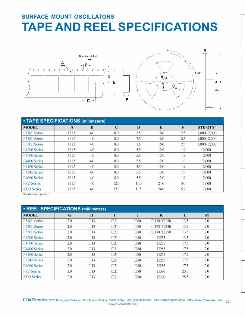
53© 2002 FOX ELECTRONICS
FOXElectronics 5570 Enterprise Parkway Fort Myers, Florida 33905 USA +001(239)693-0099 FAX +001(239)693-1554 http://www.foxonline.com
SURFACE MOUNT OSCILLATORS
TAPE AND REEL SPECIFICATIONS
1 Standard reel quantity.
TAPE SPECIFICATIONS (millimeters)MODELF510L SeriesF540L SeriesF530L SeriesF4200 SeriesF4500 SeriesF4400 SeriesF4100 SeriesF3345 SeriesF4600 SeriesFSO SeriesKFO Series
A∅ 1.5∅ 1.5∅ 1.5∅ 1.5∅ 1.5∅ 1.5∅ 1.5∅ 1.5∅ 1.5∅ 1.5∅ 1.5
B4.04.04.04.04.04.04.04.04.04.04.0
C8.08.08.08.08.08.08.08.08.012.012.0
D7.57.57.55.55.55.55.55.55.511.511.5
E16.016.016.012.012.012.012.012.012.024.024.0
F2.52.52.51.91.91.91.91.91.95.05.2
STD QTY1
1,000 / 2,0001,000 / 2,0001,000 / 2,000
2,0002,0002,0002,0002,0002,0001,0001,000
REEL SPECIFICATIONS (millimeters)MODELF510L SeriesF540L SeriesF530L SeriesF4200 SeriesF4500 SeriesF4400 SeriesF4100 SeriesF3345 SeriesF4600 SeriesFSO SeriesKFO Series
H∅ 13∅ 13∅ 13∅ 13∅ 13∅ 13∅ 13∅ 13∅ 13∅ 13∅ 13
G2.02.02.02.02.02.02.02.02.02.02.0
L13.513.513.513.517.517.517.517.517.525.525.5
M2.02.02.02.02.02.02.02.02.02.02.0
I∅ 21∅ 21∅ 21∅ 21∅ 21∅ 21∅ 21∅ 21∅ 21∅ 21∅ 21
J∅ 80∅ 80∅ 80∅ 80∅ 80∅ 80∅ 80∅ 80∅ 80∅ 80∅ 80
K∅ 178 / ∅ 250∅ 178 / ∅ 250∅ 178 / ∅ 250
∅ 255∅ 255∅ 255∅ 255∅ 255∅ 255∅ 330∅ 330

54 FOXElectronics 5570 Enterprise Parkway Fort Myers, Florida 33905 USA +001(239)693-0099 FAX +001(239)693-1554 http://www.foxonline.com© 2002 FOX ELECTRONICS
TCXOs, VCXOs AND OCXOs
SELECTION GUIDE• SURFACE MOUNT AND THRU-HOLE VCXOsPRODUCT
Frequency RangeFrequency StabilityPullabilityTemperature Range
Key Features
Catalog Pages
VCSAXT Series
1.000 ~ 77.760 MHz±25 PPM±100 PPM, ±50 PPM-10°C ~ +70°C-40ºC ~ +85ºC (Option)• 7.5 x 5mm• 3.3V Operation• HCMOS Output• Enable/Disable
Page 56
VCXO-D
1.000 ~ 40.500 MHz±2.5 PPM
-10°C ~ +70°C-40ºC ~ +85C (Option)• 14-Pin DIP• 3.3V Operation• HCMOS Output• Low Power Consumption
Page 57
VCXO-C
1.000 ~ 40.000 MHz±2.5 PPM
-10°C ~ +70°C-40ºC ~ +85ºC (Option)• 14-Pin DIP• 5.0V Operation• HCMOS/TTL Output• Rugged Resistance Weld
Page 58
• SURFACE MOUNT TCXOsPRODUCT
Frequency RangeFrequency StabilityTemperature Range
Key Features
Catalog Pages
FOX914 Series
12.600 ~ 26.000 MHz±2.5 PPM-20°C ~ +75°C• 5 x 3.2mm• 1.5mm Height Max• 3.0V Operation• Clipped Sine Output• VCTCXO
Page 59
FOX307H
10.000 ~ 26.000 MHz±2.5 PPM-20°C ~ +75°C• 7 x 5mm• 1.9mm Height Max• 3.0V Operation• Clipped Sine Output• VCTCXO
Page 60
FOX312BE
12.600 ~ 26.000 MHz±2.5 PPM-20°C ~ +75°C• 7 x 5mm• 2.0mm Height Max• 3.0V Operation• Clipped Sine Output• VCTCXO
Page 61
FOX801 Series
10.000 ~ 22.000 MHz±2.5 PPM-30°C ~ +75°C• 11.4 x 9.6mm• 2.0mm Height Max• 3.0 / 5.0V Operation• Clipped Sine Output• TCXO or VCTCXO
Page 63
• THRU-HOLE TCXOs and OCXOsPRODUCT
Frequency RangeFrequency StabilityTemperature RangeKey Features
Catalog Pages
FOX781B
8.000 ~ 20.000 MHz±2.5 PPM-20°C ~ +75°C• 14-Pin DIP• 5.0V Operation• Clipped Sine Output• TCXO or VCTCXO• Up to 45 MHz Available
Page 64
FOX782
8.000 ~ 20.000 MHz±2.5 PPM-20°C ~ +75°C• 14-Pin DIP• 5.0V Operation• HCMOS Output• TCXO or VCTCXO• Up to 45 MHz Available
Page 65
FTS501AH
10.000 ~ 40.000 MHz±250 PPB0°C ~ +70°C• 14-Pin DIP• 5.0V Operation• HCMOS/TTL Output• Meets Stratum III
Page 66-67
Sto
ckin
g S
td.
Sto
ckin
g S
td.
VC
XO
s &
TC
XO
s

55© 2002 FOX ELECTRONICS
FOXElectronics 5570 Enterprise Parkway Fort Myers, Florida 33905 USA +001(239)693-0099 FAX +001(239)693-1554 http://www.foxonline.com
FEATURES• 3.3V Operation• Stocking Standard• HCMOS Output• Enable/Disable• Tape and Reel (2,000 pcs. STD)
3.3V LOW PROFILE SMD VCXO
VCS25AXT
1 Custom specifications from 45.000 to 77.760 MHz available on an individual inquiry basis.3 Other temperature ranges, stabilities, and pullabilities available. See Page 56.Note: A 0.01µF bypass capacitor should be placed between VDD (Pin 6) and GND (Pin 3) to minimize power supply line noise.All specifications subject to change without notice. Rev. 05/01/02
See page 69 for tape and reel specifications.
OUTPUT (Pin 4)ACTIVEACTIVEHigh Z
• ENABLE / DISABLE FUNCTION 2
Pin 2OPEN'1' Level VIH ≥ 2.7 V'0' Level VIL ≤ 0.3 V
• DISTRIBUTOR STOCKING ITEMS
4.0968.19212.28816.38427.00035.32844.736
VCS25AXT-0496VCS25AXT-081VCS25AXT-128VCS25AXT-163VCS25AXT-270VCS25AXT-353VCS25AXT-447
Model Number Frequency (MHz)
1.000 ~ 77.7601 MHz
-10ºC ~ +70ºC3
-40ºC ~ +85ºC±50PPM3
±100PPM3
3.3V ± 10%1.65V ± 1.5V
15mA25mA50mA
40% ~ 60%5nS5nS
10% VDD
90% VDD Min4.0mA Min-1.0mA Min
15pF10mS150nS±10%
20 kHz
PARAMETERSFrequency Range (FO)Temperature Range Operating (TOPR) Storage (TSTG)Frequency StabilityPullabilitySupply Voltage (VDD)Control Voltage (VC)Input Current (IDD) 1.000 ~ 30.000 MHz 30.000+ ~ 45.000 MHz 45.000+ ~ 77.760 MHzOutput Symmetry (50% VDD)Rise Time (10% ~ 90% VDD) (TR)Fall Time (90% ~ 10% VDD) (TF)Output Voltage (VOL)
(VOH)Output Current (IOL)
(IOH)Output Load (HCMOS)Start-up Time (TS)Enable/Disable Time 2
Frequency LinearityModulation Bandwidth
• ELECTRICAL CHARACTERISTICS
All dimensions are in millimeters.
MAX (unless otherwise noted)
VC
XO
s & T
CX
Os
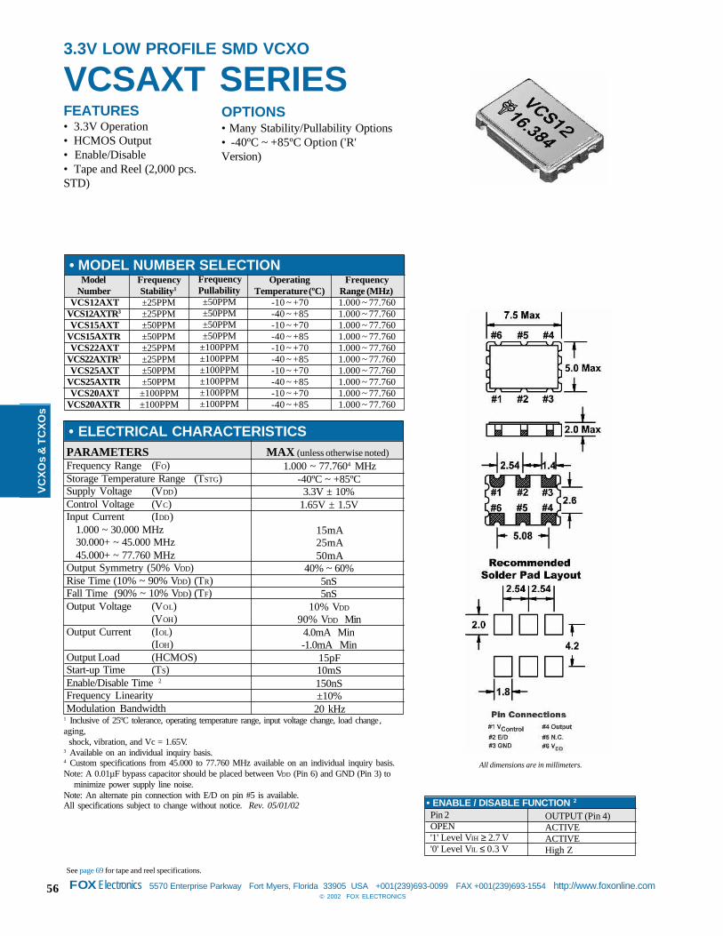
56 FOXElectronics 5570 Enterprise Parkway Fort Myers, Florida 33905 USA +001(239)693-0099 FAX +001(239)693-1554 http://www.foxonline.com© 2002 FOX ELECTRONICS
FEATURES• 3.3V Operation• HCMOS Output• Enable/Disable• Tape and Reel (2,000 pcs.STD)
3.3V LOW PROFILE SMD VCXO
VCSAXT SERIES
1 Inclusive of 25ºC tolerance, operating temperature range, input voltage change, load change,aging, shock, vibration, and Vc = 1.65V.3 Available on an individual inquiry basis.4 Custom specifications from 45.000 to 77.760 MHz available on an individual inquiry basis.Note: A 0.01µF bypass capacitor should be placed between VDD (Pin 6) and GND (Pin 3) to minimize power supply line noise.Note: An alternate pin connection with E/D on pin #5 is available.All specifications subject to change without notice. Rev. 05/01/02
See page 69 for tape and reel specifications.
OUTPUT (Pin 4)ACTIVEACTIVEHigh Z
• ENABLE / DISABLE FUNCTION 2
Pin 2OPEN'1' Level VIH ≥ 2.7 V'0' Level VIL ≤ 0.3 V
FrequencyStability1
±25PPM±25PPM±50PPM±50PPM±25PPM±25PPM±50PPM±50PPM±100PPM±100PPM
• MODEL NUMBER SELECTIONOperating
Temperature (ºC)-10 ~ +70-40 ~ +85-10 ~ +70-40 ~ +85-10 ~ +70-40 ~ +85-10 ~ +70-40 ~ +85-10 ~ +70-40 ~ +85
FrequencyRange (MHz)1.000 ~ 77.7601.000 ~ 77.7601.000 ~ 77.7601.000 ~ 77.7601.000 ~ 77.7601.000 ~ 77.7601.000 ~ 77.7601.000 ~ 77.7601.000 ~ 77.7601.000 ~ 77.760
VCS12AXTVCS12AXTR3
VCS15AXTVCS15AXTRVCS22AXT
VCS22AXTR3
VCS25AXTVCS25AXTRVCS20AXT
VCS20AXTR
ModelNumber
FrequencyPullability±50PPM±50PPM±50PPM±50PPM
±100PPM±100PPM±100PPM±100PPM±100PPM±100PPM
1.000 ~ 77.7604 MHz-40ºC ~ +85ºC
3.3V ± 10%1.65V ± 1.5V
15mA25mA50mA
40% ~ 60%5nS5nS
10% VDD
90% VDD Min4.0mA Min-1.0mA Min
15pF10mS150nS±10%
20 kHz
PARAMETERSFrequency Range (FO)Storage Temperature Range (TSTG)Supply Voltage (VDD)Control Voltage (VC)Input Current (IDD) 1.000 ~ 30.000 MHz 30.000+ ~ 45.000 MHz 45.000+ ~ 77.760 MHzOutput Symmetry (50% VDD)Rise Time (10% ~ 90% VDD) (TR)Fall Time (90% ~ 10% VDD) (TF)Output Voltage (VOL)
(VOH)Output Current (IOL)
(IOH)Output Load (HCMOS)Start-up Time (TS)Enable/Disable Time 2
Frequency LinearityModulation Bandwidth
• ELECTRICAL CHARACTERISTICS
All dimensions are in millimeters.
MAX (unless otherwise noted)
OPTIONS• Many Stability/Pullability Options• -40ºC ~ +85ºC Option ('R'Version)
VC
XO
s &
TC
XO
s

57© 2002 FOX ELECTRONICS
FOXElectronics 5570 Enterprise Parkway Fort Myers, Florida 33905 USA +001(239)693-0099 FAX +001(239)693-1554 http://www.foxonline.com
VC
XO
s & T
CX
Os
OPTIONS• Many Stability/Pullability Options• -40ºC ~ +85ºC Option ('R'Version)
FEATURES• 3.3V Operation• HCMOS Output• Low Power Consumption• Rugged Resistance Weld
3.3V THRU-HOLE VOLTAGE CONTROLLED CRYSTAL OSCILLATOR
VCXO-D
1 Inclusive of 25ºC tolerance, operating temperature range, input voltage change, load change,aging, shock, vibration, and Vc = 1.65V.3 Higher frequencies available on an individual inquiry basis.All specifications subject to change without notice. Rev. 05/01/02
1.000 ~ 40.5003 MHz-55ºC ~ +125ºC
3.3V ± 5%1.65V ± 1.65V
10mA15mA25mA
40% ~ 60%10nS10nS
10% VDD
90% VDD Min4.0mA Min-1.0mA Min
15pF10mS±10%
PARAMETERSFrequency Range (FO)Storage Temperature Range (TSTG)Supply Voltage (VDD)Control Voltage (VC)Input Current (IDD) 1.000 ~ 24.000 MHz 24.000+ ~ 35.000 MHz 35.000+ ~ 40.500 MHzOutput Symmetry (50% VDD)Rise Time (10% ~ 90% VDD) (TR)Fall Time (90% ~ 10% VDD) (TF)Output Voltage (VOL)
(VOH)Output Current (IOL)
(IOH)Output Load (HCMOS)Start-up Time (TS)Frequency Linearity
• ELECTRICAL CHARACTERISTICS
All dimensions are in millimeters.
FrequencyStability1
±50PPM±50PPM±25PPM±25PPM±25PPM±25PPM±100PPM±100PPM
• MODEL NUMBER SELECTIONOperating
Temperature (ºC)-10 ~ +70-40 ~ +85-10 ~ +70-40 ~ +85-10 ~ +70-40 ~ +85-10 ~ +70-40 ~ +85
FrequencyRange (MHz)1.000 ~ 40.5001.000 ~ 40.5001.000 ~ 40.5001.000 ~ 40.5001.000 ~ 40.5001.000 ~ 40.5001.000 ~ 40.5001.000 ~ 40.500
VCXO-D3VCXO-D3RVCXO-D4
VCXO-D4RVCXO-D7
VCXO-D7RVCXO-D8
VCXO-D8R
ModelNumber
FrequencyPullability±100PPM±100PPM±100PPM±100PPM±50PPM±50PPM±100PPM±100PPM
MAX (unless otherwise noted)

58 FOXElectronics 5570 Enterprise Parkway Fort Myers, Florida 33905 USA +001(239)693-0099 FAX +001(239)693-1554 http://www.foxonline.com© 2002 FOX ELECTRONICS
FEATURES• 5.0V Operation• HCMOS/TTL Output• Rugged Resistance Weld
5.0V THRU-HOLE VOLTAGE CONTROLLED CRYSTAL OSCILLATOR
VCXO-C
1 Inclusive of 25ºC tolerance, operating temperature range, input voltage change, load change,aging, shock, vibration, and Vc = 2.5V.3 Higher frequencies available on an individual inquiry basis.All specifications subject to change without notice. Rev. 05/01/02
FrequencyStability1
±50PPM±50PPM±50PPM±50PPM±25PPM±25PPM±25PPM±25PPM±100PPM±100PPM
• MODEL NUMBER SELECTIONOperating
Temperature (ºC)-10 ~ +70-40 ~ +85-10 ~ +70-40 ~ +85-10 ~ +70-40 ~ +85-10 ~ +70-40 ~ +85-10 ~ +70-40 ~ +85
FrequencyRange (MHz)1.000 ~ 40.0001.000 ~ 40.0001.000 ~ 40.0001.000 ~ 40.0001.000 ~ 40.0001.000 ~ 40.0001.000 ~ 40.0001.000 ~ 40.0001.000 ~ 40.0001.000 ~ 40.000
VCXO-C2VCXO-C2RVCXO-C3
VCXO-C3RVCXO-C4
VCXO-C4RVCXO-C7
VCXO-C7RVCXO-C8
VCXO-C8R
ModelNumber
FrequencyPullability±200PPM±200PPM±100PPM±100PPM±100PPM±100PPM±50PPM±50PPM
±100PPM±100PPM
1.000 ~ 40.0003 MHz-40ºC ~ +85ºC
5.0V ± 5%2.5V ± 2V
15mA20mA30mA
40% ~ 60%10nS10nS
10% VDD
90% VDD Min3.2mA Min-0.1mA Min
8 LSTTL15pF10mS
-125 dBc/Hz-130 dBc/Hz
±1.0PPM±10%10kHz
PARAMETERSFrequency Range (FO)Storage Temperature Range (TSTG)Supply Voltage (VDD)Control Voltage (VC)Input Current (IDD) 1.000 ~ 24.000 MHz 24.000+ ~ 30.000 MHz 30.000+ ~ 40.000 MHzOutput Symmetry (50% VDD)Rise Time (10% ~ 90% VDD) (TR)Fall Time (90% ~ 10% VDD) (TF)Output Voltage (VOL)
(VOH)Output Current (IOL)
(IOH)Output Load TTL HCMOSStart-up Time (TS)Phase Noise Fo + 1 kHz Fo + 10 kHzStability vs. Voltage (VDD = 5.0V± 5%)LinearityModulation
• ELECTRICAL CHARACTERISTICS
All dimensions are in millimeters.
MAX (unless otherwise noted)
OPTIONS• Many Stability/Pullability Options• -40ºC ~ +85ºC Option ('R'Version)
VC
XO
s &
TC
XO
s

59© 2002 FOX ELECTRONICS
FOXElectronics 5570 Enterprise Parkway Fort Myers, Florida 33905 USA +001(239)693-0099 FAX +001(239)693-1554 http://www.foxonline.com
FEATURES• 3.0V Operation• 1.5mm Height Max• Clipped Sine Output• Low Cost• Tape and Reel (2,000 pcs. STD)
3.0V ULTRA MINIATURE SMD TCXO/VCTCXO
FOX914 SERIES
See page 69 for tape and reel specifications.
• DEVELOPED FREQUENCIES1
12.600 MHz12.800 MHz13.000 MHz13.824 MHz14.400 MHz14.850 MHz16.800 MHz
19.200 MHz19.440 MHz19.680 MHz19.800 MHz20.000 MHz26.000 MHz
OPTIONS• Voltage Control (FOX914E)• Lower Voltages
1 Undeveloped frequencies available on an inquiry basis.2 For proper operation, a control voltage (Vc) must be applied to pin 1 on VCTCXOs.All specifications subject to change without notice. Rev. 05/01/02
12.600 ~ 26.000 MHz
-20ºC ~ +75ºC-40ºC ~ +85ºC
3.0V ± 5%2.0mA
±0.5PPM
±2.5PPM±0.2PPM±0.2PPM
0.8V Min10kΩ // 10pF
±1.0PPM±5.0 ~ ±15.0 PPM
PARAMETERSFrequency Range (FO)Temperature Range Operating (TOPR) Storage (TSTG)Supply Voltage (VDD)Input Current (IDD)Initial Frequency Tolerance (@ 25ºC ± 2ºC) (Vc = 1.5V)2
Frequency Stability Over Temperature Range Over Supply Voltage Change (3.0V ± 5%) Over Load Change (10Ω ± 10% // 10pF ±10%)Output Waveform (Clipped Sine) Peak-to-Peak Level (Vp-p)Output LoadAging per yearPullability2 (Vc = 1.5 ± 1.0V)
• ELECTRICAL CHARACTERISTICSMAX (unless otherwise noted)
All dimensions are in millimeters.
VC
XO
s & T
CX
Os

60 FOXElectronics 5570 Enterprise Parkway Fort Myers, Florida 33905 USA +001(239)693-0099 FAX +001(239)693-1554 http://www.foxonline.com© 2002 FOX ELECTRONICS
FEATURES• 3.0V Operation• 1.9mm Height Max• Clipped Sine Output• Tape and Reel (2,000 pcs. STD)
3.0V SMD TCXO/VCTCXO
FOX307H
1 For proper operation, a control voltage (Vc) must be applied to pin 1.All specifications subject to change without notice. Rev. 05/01/02
See page 69 for tape and reel specifications.
All dimensions are in millimeters.
10.000 ~ 26.000 MHz
-20ºC ~ +75ºC-40ºC ~ +85ºC
3.0V ± 5%2.0mA
±2.5PPM±0.3PPM±0.3PPM
±5.0 ~ ±15.0PPM
0.8V Min10kΩ // 10pF
±1.0PPM
PARAMETERSFrequency Range (FO)Temperature Range Operating (TOPR) Storage (TSTG)Supply Voltage (VDD)Input Current (IDD)Frequency Stability Over Temperature Range Over Supply Voltage Change (3.0V ± 5%) Over Load Change (10ς // 10pF)Voltage Control1 (1.5V ± 1.0V)Output Waveform (Clipped Sine) Peak-to-Peak Level (Vp-p)Output LoadAging per year
• ELECTRICAL CHARACTERISTICSMAX (unless otherwise noted)
VC
XO
s &
TC
XO
s

61© 2002 FOX ELECTRONICS
FOXElectronics 5570 Enterprise Parkway Fort Myers, Florida 33905 USA +001(239)693-0099 FAX +001(239)693-1554 http://www.foxonline.com
See page 69 for tape and reel specifications.
3.0V LOW PROFILE SMD VCTCXO
FOX312BEFEATURES• 3.0V Operation• 2.0mm Height Max• Clipped Sine Output• Tape and Reel (1,000 pcs.STD)
1 For proper operation, a control voltage (Vc) must be applied to pin 1.All specifications subject to change without notice. Rev. 05/01/02
12.600 ~ 26.000 MHz
-20ºC ~ +75ºC-40ºC ~ +85ºC
3.0V ± 5%2.0mA
±2.5PPM±0.1PPM±0.3PPM
±0.5PPM
0.8V Min10KΩ // 10pF
±5.0 ~ ±15.0PPM±1.0PPM
PARAMETERSFrequency Range (FO)Temperature Range Operating (TOPR) Storage (TSTG)Supply Voltage (VDD)Input Current (IDD)Frequency Stability Over Temperature Range Over Supply Voltage Change (3.0V ± 5%) Over Load Change (10KΩ±10% // 10pF±10%)Initial Frequency Tolerance @ 25ºC Vc = 1.5V1
Output Waveform (Clipped Sine) Peak-to-Peak Level (Vp-p)Output LoadPullability1 (1.5V ± 1.0V)Aging per year
• ELECTRICAL CHARACTERISTICSMAX (unless otherwise noted)
All dimensions are in millimeters.
VC
XO
s & T
CX
Os

62 FOXElectronics 5570 Enterprise Parkway Fort Myers, Florida 33905 USA +001(239)693-0099 FAX +001(239)693-1554 http://www.foxonline.com© 2002 FOX ELECTRONICS
FEATURES• 3.0V Operation• 2.0mm Height Max• Clipped Sine Output• Low Cost• Stocking Standard• Tape and Reel (2,000 pcs.STD)
3.0V LOW PROFILE VCTCXO
FOX801BE
See page 69 for tape and reel specifications.
• DISTRIBUTOR STOCKING ITEMS
10.00012.80014.40016.00019.200
FOX801BE-100FOX801BE-128FOX801BE-144FOX801BE-160FOX801BE-192
Model Number Frequency (MHz)
1 For proper operation, a control voltage (Vc) must be applied to pin 1 on VCTCXOs.All specifications subject to change without notice. Rev. 05/01/02
10.000 ~ 22.000 MHz
-30ºC ~ +75ºC-35ºC ~ +85ºC
±0.5PPM3.0V ± 5%
2.0mA
±2.5PPM±0.3PPM±0.3PPM
±3.0PPM Min
0.8V Min0.7V Min
10KΩ // 10pF±3.0PPM±0.8PPM
PARAMETERSFrequency Range (FO)Temperature Range Operating (TOPR) Storage (TSTG)Frequency Tolerance (@25ºC) Vc = 1.5V1
Supply Voltage (VDD)Input Current (IDD)Frequency Stability Over Temperature Range Over Supply Voltage Change (3.0V ± 5%) Over Load Change (10Ω ± 10% // 10pF ±10%)Voltage Control1 (1.5V ± 1.0V)Output Waveform (Clipped Sine) Peak-to-Peak Level (Vp-p) 10.000 ~ 14.400 14.400+ ~ 22.000Output LoadFrequency Adjustment (Internal Trimmer)Aging per year
• ELECTRICAL CHARACTERISTICSMAX (unless otherwise noted)
All dimensions are in millimeters.
VC
XO
s &
TC
XO
s

63© 2002 FOX ELECTRONICS
FOXElectronics 5570 Enterprise Parkway Fort Myers, Florida 33905 USA +001(239)693-0099 FAX +001(239)693-1554 http://www.foxonline.com
FEATURES• 2.0mm Height Max• Low Cost• Clipped Sine Output• Tape and Reel (2,000 pcs. STD)
3.0V/5.0V LOW PROFILE TCXO
FOX801 SERIES
All dimensions are in millimeters.
1 For proper operation, a control voltage (Vc) must be applied to pin 1 on VCTCXOs.All specifications subject to change without notice. Rev. 05/01/02
10.000 ~ 22.000 MHz
-30ºC ~ +75ºC-35ºC ~ +80ºC
±0.5PPM±2.0PPM
5.0V ± 5%3.0V ± 5%
2.0mA
±2.5PPM±0.3PPM±0.3PPM
1.0V Min0.8V Min0.7V Min
10KΩ // 10pF
±3.0PPMTrimmerless
None±5.0PPM Min±8.0PPM Min
±0.8PPM
PARAMETERSFrequency Range (FO)Temperature Range Operating (TOPR) Storage (TSTG)Initial Frequency Tolerance (@25ºC) Vc = 2.5V (A Series)1 FOX801A/B/AE/BE Vc = 1.5V (B Series)1 FOX801AH/BHSupply Voltage (VDD) A Version B VersionInput Current (IDD)Frequency Stability Over Temperature Range Over Supply Voltage Change (VDD ± 5%) Over Load Change (10Ω ± 10% // 10pF ±10%)Output Waveform (Clipped Sine) Peak-to-Peak Level (Vp-p) A Version: 10.000 ~ 22.000 MHz B Version: 10.000 ~ 14.400 MHz B Version: 14.400+ ~ 22.000 MHzOutput LoadFrequency Adjustment (Internal Trimmer) FOX801A/B/AE/BE FOX801AH/BHVoltage Control Option (VCTCXO)1
A Version (Vc=2.5±2.0V) FOX801A/B B Version (Vc=1.5±1.0V) FOX801AE/BE
FOX801AH/BHAging per year 8.000 ~ 22.000
• ELECTRICAL CHARACTERISTICSMAX (unless otherwise noted)
OPTIONS• 'A' Version - 5.0V• 'B' Version - 3.3V• VCTCXO - AE/BE Version• VCTCXO - AH/BH Version
(trimmerless)
See page 69 for tape and reel specifications.
VC
XO
s & T
CX
Os

64 FOXElectronics 5570 Enterprise Parkway Fort Myers, Florida 33905 USA +001(239)693-0099 FAX +001(239)693-1554 http://www.foxonline.com© 2002 FOX ELECTRONICS
FEATURES• 5.0V Operation• Clipped Sine Output• Adjustable Frequency• 14-Pin DIP
5.0V THRU-HOLE TCXO/VCTCXO
FOX781B
1 Frequencies from 20.000+ MHz to 45.000 MHz available on an individual inquiry basis.3 VCTCXO version (FOX781C) available on an individual inquiry basis to custom customer specifications.All specifications subject to change without notice. Rev. 05/01/02
OPTIONS• VCTCXO - FOX781C• Higher Frequencies
8.000 ~ 20.0001 MHz±1.0PPM
±2.5PPM±0.2PPM±0.2PPM
-20ºC ~ +75ºC-40ºC ~ +80ºC
5.0V ± 5%
1.0V Min2.0mA
10KΩ // 10pF
±1.0PPM±2.0PPM
±3.0PPM Min
PARAMETERSFrequency Range (FO)Initial Frequency Tolerance @ 25ºCFrequency Stability Over Temperature Range Over Supply Voltage Change (5.0V ± 5%) Over Load Change (10KΩ ± 10% // 10pF10%)Temperature Range Operating (TOPR) Storage (TSTG)Supply Voltage (VDD)Output Waveform (Clipped Sine) Peak-to-Peak Level (Vp-p)Input Current (IDD)Output LoadAging @ 25ºC; per year 8.000 ~ 19.999999 MHz
20.000000 MHzFrequency Adjustment (Internal Trimmer)
• ELECTRICAL CHARACTERISTICSMAX (unless otherwise noted)
All dimensions are in millimeters.
VC
XO
s &
TC
XO
s

65© 2002 FOX ELECTRONICS
FOXElectronics 5570 Enterprise Parkway Fort Myers, Florida 33905 USA +001(239)693-0099 FAX +001(239)693-1554 http://www.foxonline.com
FEATURES• 5.0V Operation• HCMOS Output• Adjustable Frequency• 14-Pin DIP
5.0V THRU-HOLE TCXO/VCTCXO
FOX782
1 Frequencies from 20.000+ MHz to 45.000 MHz available on an individual inquiry basis.3 VCTCXO version (FOX782C) available on an individual inquiry basis to custom customer specifications.All specifications subject to change without notice. Rev. 05/01/02
OPTIONS• VCTCXO - FOX782C• Higher Frequencies• 3.3V (FOX782A)
8.000 ~ 20.000 MHz±1.0PPM
±2.5PPM±0.2PPM
-20ºC ~ +75ºC-40ºC ~ +80ºC
5.0V ± 5%
15mA40% ~ 60%
5nS5nS
10% VDD
90% VDD Min4.0mA Min-1.0mA Min
15pF10mS
PARAMETERSFrequency Range (FO)Initial Frequency Tolerance @ 25ºCFrequency Stability Over Temperature Range Over Supply Voltage Change (5.0V ± 5%)Temperature Range Operating (TOPR) Storage (TSTG)Supply Voltage (VDD)Input Current (IDD) 8.000 ~ 20.000 MHzOutput Symmetry (50% VDD)Rise Time (10% ~ 90% VDD) (TR)Fall Time (90% ~ 10% VDD) (TF)Output Voltage (VOL)
(VOH)Output Current (IOL)
(IOH)Output Load (HCMOS)Start-up Time (TS)
• ELECTRICAL CHARACTERISTICSMAX (unless otherwise noted)
All dimensions are in millimeters.
VC
XO
s & T
CX
Os

66 FOXElectronics 5570 Enterprise Parkway Fort Myers, Florida 33905 USA +001(239)693-0099 FAX +001(239)693-1554 http://www.foxonline.com© 2002 FOX ELECTRONICS
OC
XO
sOVEN CONTROLLED CRYSTAL OSCILLATORS (OCXO)
GENERAL DESIGN SPECIFICATIONS
As Fox ventures into the OCXO product offerings, we have established a General Specification Matrixof products we currently have in development. In addition to the matrix, we can develop new OCXOsbased on customer needs. To discuss your OCXO requirements, contact the Fox Customer TechnologyCenter (CTC) referenced on the inside covers of this catalog.
PRELIMINARY
10.000 ~ 125.000 MHz±250 ~ ±750 PPB
0ºC ~ +70ºC, -40ºC ~ +75ºC3.3V, 5.0V
HCMOS, Sine Wave
Frequency RangeStabilityTemperature RangeSupply VoltagesOutput Type
• 14-PIN DIP
5.000 ~ 125.000 MHz±4 ~ ±120 PPB
0ºC ~ +50ºC, -40ºC ~ +75ºC5.0V, 12.0V
HCMOS, Sine Wave
Frequency RangeStabilityTemperature RangeSupply VoltagesOutput Type
• EURO PACKAGE
* Current Capabilities not yet in production.* All specifications to be confirmed at prototype.Rev. 05/01/02
5.000 ~ 125.000 MHz±4 ~ ±120 PPB
0ºC ~ +50ºC, -40ºC ~ +75ºC5.0V, 12.0V
HCMOS, Sine Wave
Frequency RangeStabilityTemperature RangeSupply VoltagesOutput Type
• 38.1 x 38.1mm PACKAGE
5.000 ~ 125.000 MHz±4 ~ ±120 PPB
0ºC ~ +50ºC, -40ºC ~ +75ºC5.0V, 12.0V
HCMOS, Sine Wave
Frequency RangeStabilityTemperature RangeSupply VoltagesOutput Type
• 50.8 x 50.8mm PACKAGE

67© 2002 FOX ELECTRONICS
FOXElectronics 5570 Enterprise Parkway Fort Myers, Florida 33905 USA +001(239)693-0099 FAX +001(239)693-1554 http://www.foxonline.com
OC
XO
sSTRATUM III 14-PIN DIP OVEN CONTROLLED CRYSTAL OSCILLATOR
FTS501AHFEATURES• Meets Stratum III• 5.0V Operation• HCMOS Output• 14-Pin DIP
1 3.3V available upon requestAll specifications subject to change without notice. Rev. 05/01/02
OPTIONS• 3.3V Available
All dimensions are in millimeters.
10.000 ~ 40.000 MHz
0ºC ~ +70ºC-40ºC ~ +85ºC
5V ±0.2V 1
HCMOS4 PPM Min0.5V ~ 5.0V±4.6 PPM
All effects for 10 years±250 PPB±100 PPB±20 PPB
±370 PPB±10 PPB
±0.75 PPM±4.2 PPM2 Minutes
< 1.5 Watts1.0W ~ 0ºC, 0.6W @ +25ºC
-115 dBc/Hz @ 100 Hz-140 dBc/Hz @ 10 kHz
PARAMETERSFrequency Range (FO)Temperature Range
Operating (TOPR)Storage (TSTG)
Supply VoltageOutput TypePullabilityControl VoltageFrequency Stabilities
Frequency vs. TemperatureFrequency vs. VoltageHoldover Aging (24 hours)Holdover StabilityLoad StabilityLong Term Aging 1st YearAging 10 YearsWarm-up to within ±4.6 PPMWarm-up PowerOperating Power (Typical)Phase Noise
• ELECTRICAL CHARACTERISTICSMAX (unless otherwise noted)

FOX Electronics - The Leader in Radio Frequency Crystal Oscillator
Radio Frequency Crystal Oscillators
The RFXO Family of Oscillators was developed by Fox Electronics Inc. for SONET/SDH/ATM/WAN applications. By combining a proprietary ASIC architecture with our advanced quartz technologies, these RFXOs are able to generate very clean output frequencies. This exclusive combination of radio frequency control technologies enables these RFXOs to deliver the optimum
cost-to-performance ratio in the industry for RF applications. See us at Electronica 2002.
RFV300Spec Sheet
RFX300Spec Sheet
RFXO Features:· Available as a standard Oscillator (XO) or Voltage controlled Crystal Oscillator (VCXO)· Frequencies from 600MHz to 1.25GHz· Industry standard SMT package (7.5x5x1.5mm Max)· LV-PECL complementary outputs· 3.3v and 2.5v versions· Output Enable/Disable function· Low jitter and phase Noise· Tight stabilities and extended temperature ranges available
RFXO Series, includes both PDFs
RFXO Applications:· PLL circuits for clock smoothing or frequency translation· SONET/SDH, ATM, WAN, OC-12 up through OC-768 including FEC rates, Gb Ethernet and Fiber Channel· Timing reference for Optical and Data Communications systems
RFXO Description: The RFXO family of Oscillators is an ASIC-driven crystal-based line of frequency control products. These RFXOs are available as standard Crystal Oscillators (XOs) or Voltage Controlled Crystal Oscillators (VCXOs) with frequencies from 600MHz to 1.25GHz. The RFXO family of products generates an output at the frequency of operation (fo) with low jitter and phase noise in the frequency domain. Low clock jitter is essential to achieve a low bit error rate in optical data communications and also allows for full use of the allotted bandwidth. This makes the RFXO ideally suited for the next generation of low jitter clocks and data streams for SONET/SDH applications.
http://www.foxonline.com/rfxoseries2.htm (1 of 2) [11/06/2002 2:54:45 PM]

FOX Electronics - The Leader in Radio Frequency Crystal Oscillator
Electronica 2002New Munich Trade Fair CenterMunich, GermanyNovember 12 ~15 November 2002
Viewing and printing of these catalog pages requires Adobe Acrobat® Reader, which can be downloaded at no cost by using this link. It is available for many platforms. Your printer setup may require an adjustment to print the entire page image.
Need Technical Support?Please include your phone number.
Copyright © 1998-2002 Fox Electronics.All rights reserved.
http://www.foxonline.com/rfxoseries2.htm (2 of 2) [11/06/2002 2:54:45 PM]

1© 2002 FOX ELECTRONICS
FOXElectronics 5570 Enterprise Parkway Fort Myers, Florida 33905 USA +001(239)693-0099 FAX +001(239)693-1554 http://www.foxonline.com
All dimensions are in millimeters.
FEATURES• 3.3V Operation• High Performance• Complementary Output
Applications include SONET / SDH / ATM / WAN
3.3V LV-PECL XO
RFX300
FrequencyStability±100PPM±100PPM±50PPM±50PPM±25PPM±25PPM±20PPM
• MODEL NUMBER SELECTIONOperating
Temperature (ºC)-20 ~ +70-40 ~ +85-20 ~ +70-40 ~ +85-20 ~ +70-40 ~ +85-20 ~ +70
RFX300RFX300RRFX305
RFX305RRFX306
RFX306RRFX308
Model Number
622 ~ 700 MHz, 1.244 ~ 1.25GHz-55ºC ~ +125ºC
3.3V ± 10%60mA0.5nS0.5nS45/55
1.305V ~ 1.65 V2.155 ~ 2.405 V
10mS125pS
<0.5pS3 pS
30 pS
PARAMETERSAvailable FrequencysStorage Temperature RangeSupply Voltage (VDD)Supply Current 3.3V VersionRise Time (20% ~ 80% Vp-p)Fall Time (80% ~ 20% Vp-p)Symmetry (50% Vp-p)Output Voltage 3.3V Version(VOL)
(VOH)Start-up Time (TS)PECL Skew (50% Vp-p)Jitter
Integrated 12kHz to 20MHzRMSCycle-to-Cycle
• ELECTRICAL CHARACTERISTICS
Inclusive of 25ºC tolerance, operating temperature range, input voltage change, load change, aging, shock, and vibration.
LV-PECL OUT
PRELIMINARY
RFX300 Series Recommended Circuit
LV-PECL OUT

2 FOXElectronics 5570 Enterprise Parkway Fort Myers, Florida 33905 USA +001(239)693-0099 FAX +001(239)693-1554 http://www.foxonline.com© 2002 FOX ELECTRONICS
FEATURES• 3.3V Operation• High Performance• Complementary Output
Applications include SONET / SDH / ATM / WAN
3.3V LV-PECL VCXO
RFV300
FrequencyStability±50PPM±50PPM±25PPM±25PPM±20PPM
• MODEL NUMBER SELECTIONOperating
Temperature (ºC)-20 ~ +70-40 ~ +85-20 ~ +70-40 ~ +85-20 ~ +70
RFV350RFV350RRFV325
RFV325RRFV330
Model Number
622 ~ 700 MHz, 1.244 ~ 1.25GHz-55ºC ~ +125ºC
3.3V ± 10%60mA0.5nS0.5nS45/55
1.305V ~ 1.65 V2.155 ~ 2.405 V
10mS± 10%
>10kHz125pS
<0.5pS3 pS30 pS
PARAMETERSAvailable FrequencysStorage Temperature RangeSupply Voltage (VDD)Supply Current 3.3V VersionRise Time (20% ~ 80% Vp-p)Fall Time (80% ~ 20% Vp-p)Symmetry (50% Vp-p)Output Voltage 3.3V Version(VOL)
(VOH)Start-up Time (TS)LinearityModulation BandwidthPECL Skew (50% Vp-p)Jitter
Integrated 12kHz to 20MHzRMSCycle-to-Cycle
• ELECTRICAL CHARACTERISTICS
Inclusive of 25ºC tolerance, operating temperature range, input voltage change, load change, aging, shock, and vibration.
FrequencyPullability±100PPM±100PPM±50PPM±50PPM±50PPM
All dimensions are in millimeters.
PRELIMINARY
RFV300 Series Recommended Circuit
LV-PECL OUT
LV-PECL OUT

68 FOXElectronics 5570 Enterprise Parkway Fort Myers, Florida 33905 USA +001(239)693-0099 FAX +001(239)693-1554 http://www.foxonline.com© 2002 FOX ELECTRONICS
Fox
Ele
ctro
nic
s P
art
Des
crip
tio
n1
Gu
ide
for
TC
XO
s/V
CX
Os
1M
ake
Sel
ectio
n fr
omP
rodu
ct F
amily
in F
ox C
atal
og o
rF
oxon
line.
com
For
Exa
mpl
e: F
ox80
1B
2F
req
uen
cy M
Hz
Cus
tom
er F
ills
In
3S
tab
ility
2
Pic
k fr
omS
ectio
n A
4O
per
atin
gTe
mp
2
7S
MD
Pac
kag
ing
8 Fox
Use
9/10
Valu
eA
dd
ed
11C
ust
om
Sect
ion
A
A ±
100
ppm
B ±
50
ppm
C ±
30p
pmD
± 2
5ppm
E ±
20p
pmF
± 1
5ppm
G ±
12p
pmH
± 1
0ppm
J ±
7.5
ppm
K ±
7pp
mL
± 5
ppm
M ±
4pp
mN
± 3
ppm
P ±
2.5
ppm
R ±
2pp
mS
± 1
.5pp
mT
± 1
ppm
U ±
0.5
ppm
Ope
ratin
g Te
mp.
Ran
ge
A =
0º
to +
50ºC
B =
-10
º to
+50
ºCC
= 0
º to
+70
ºCD
= -
10º
to +
60ºC
E =
-10
º to
+70
ºCF
= -
20º
to +
70ºC
Z =
-25
º to
+75
ºCG
= -
30º
to +
70ºC
H =
-30
º to
+75
ºCJ
= -
30º
to +
80ºC
K =
-30
º to
+85
ºCL
= -
35º
to +
80ºC
V =
-35
º to
+85
ºCM
= -
40º
to +
85ºC
SMD
Pac
kagi
ng
0 =
Tap
e/R
eel*
250
= 2
5050
0 =
500
1000
= 1
000
Tape
Onl
y =
Tap
e O
nly
Val
ue A
dded
M =
Spe
cial
Mar
king
N =
Cut
Bas
eS
= B
ulk
Z =
SM
D t
ape
Cus
tom
C =
Cus
tom
Pla
ce a
ttac
h dr
awin
gan
d/or
add
itio
nal
elec
tric
al s
pecs
for
our
engi
neer
ing
depa
rtm
ent.
5/6
Fox
Use
(###
#.##
####
)
Not
es:
1 Fox
uni
que
part
num
bers
for
non
-sta
ndar
ds a
re r
ando
mly
gen
erat
ed b
ased
on
the
elem
ents
of
the
par
t de
scri
ptio
n in
a f
orm
at:
###
- Fr
eque
ncy
- R
ando
m #
(09
9-22
.118
4-39
789
is F
ox u
niqu
e
p
art
num
ber)
.
2 All
com
bina
tion
s ar
e no
t po
ssib
le.
*
0 =
Tap
e/R
eel
assu
mes
tha
t no
qua
ntity
per
ree
l w
as s
peci
fied
: t
here
fore
, the
Fox
Pro
duct
ion
SMD
Ree
l Q
uant
ities
lis
t ap
plie
s.
For
any
othe
r qu
antit
ies
spec
ifie
d a
brok
en r
eel
char
ge w
ill a
pply
.
Fox
Prod
uctio
n SM
D R
eel
Qua
ntiti
es
759/
739
Ser
ies
1KF
5000
/F51
00 S
erie
s1K
FO
X80
1 S
erie
s2K
FO
X30
5B S
erie
s1K
FO
X31
2BE
Ser
ies
1KV
CS
Seri
es2K

69© 2002 FOX ELECTRONICS
FOXElectronics 5570 Enterprise Parkway Fort Myers, Florida 33905 USA +001(239)693-0099 FAX +001(239)693-1554 http://www.foxonline.com
SURFACE MOUNT VCXOs and TCXOs
TAPE AND REEL SPECIFICATIONS
1 Standard reel quantity.
TAPE SPECIFICATIONS (millimeters)MODELVCSAXT SeriesFOX914 SeriesFOX307HFOX312BEFOX801 Series
A∅ 1.5∅ 1.5∅ 1.5∅ 1.5∅ 1.5
B4.04.04.04.04.0
C8.08.08.08.012.0
D5.55.57.57.511.5
E12.012.016.016.024.0
F1.91.72.52.22.7
STD QTY1
2,0002,0002,0001,0002,000
REEL SPECIFICATIONS (millimeters)MODELVCSAXT SeriesFOX914 SeriesFOX307HFOX312BEFOX801 Series
G2.02.02.02.02.0
H∅ 13∅ 13∅ 13∅ 13∅ 13
I∅ 21∅ 21∅ 25∅ 21∅ 21
J∅ 80∅ 100∅ 80∅ 100∅ 80
K∅ 255∅ 254∅ 255∅ 330∅ 330
L17.513.517.516.425.5
M2.02.02.02.01.6

70 FOXElectronics 5570 Enterprise Parkway Fort Myers, Florida 33905 USA +001(239)693-0099 FAX +001(239)693-1554 http://www.foxonline.com© 2002 FOX ELECTRONICS
Fox filters offer excellent features such as sharp cut off characteristics,low loss and high stability over a wide temperature range which aresuperior to LC Filters and Ceramic Filters.
The basic building block for all custom built Fox filters is the two-pole monolithic filter available in standard package as shown. Two-pole monolithic filters are cascaded to produce four, six and eightpole filter responses with the addition of coupling capacitorsbetween two-pole sections. Standard Fox filters are available withcenter frequencies from 10.7 MHz to 90 MHz, and from two toeight poles.
For custom made filters, please specify the following: Holder Size Nominal Frequency Pass Bandwidth
Note: 45F Series 45.000 MHz fundamental is a special filter designed for mobileradio and cellular phone applications.
Insertion Loss Attenuation Spurious Response
Ripple Terminating Impedance Operating Temp. Range
MONOLITHIC CRYSTAL
FILTERS
MULTI-POLE PACKAGE DIMENSIONSCASE TYPECDCN
L0.590 (15.0)0.728 (18.5)0.433 (11.0)
H0.591 (15.0)0.591 (15.0)0.453 (11.5)
A0.354 (9.0)0.531 (13.5)0.291 (7.4)
B0.197 (5.0)0.197 (5.0)0.157 (4.0)
W0.472 (12.0)0.472 (12.0)0.335 (8.5)
FILT
ERS

71© 2002 FOX ELECTRONICS
FOXElectronics 5570 Enterprise Parkway Fort Myers, Florida 33905 USA +001(239)693-0099 FAX +001(239)693-1554 http://www.foxonline.com
Type
10M7A
10M7B
10M7C10M7D10M12A
10M12B
10M12C10M12D10M15A
10M15B
10M15C10M15D10M20A
10M20B
16M15A
16M15B
16M15C16M15D21M7A
21M7B
21M7C21M7D21M12A
21M12B
21M12C21M12D21M15A
21M15B
21M15C21M15D21M20A
21M20B
21M30A
21M30B
45F15A
45F15B
45F20A
45F20B
45F30A
45F30B
45M15A
45M15B
45M20A
45M20B
70M15A
70M15B
70M20A
70M20B
TerminatingImpedanceohms/pF
1.8K//6.0
1.8K//5.0Cc = 11pF1.8K//5.01.8K//5.03.3K//1.5
3.3K//1.5Cc = 6pF3.3K//2.03.3K//2.03.0K//2.0
3.0K//2.0Cc = 5pF3.3K//1.53.3K//1.53.9K//1.0
3.9K//1.0Cc = 3pF1.8K//2.0
1.8K//1.5Cc = 7.5pF1.8K//1.51.8K//1.5850//6.0
850//5.0Cc = 16pF850//5.0850//5.01.2K//3.0
1.2K//2.5Cc = 10.5pF1.2K//2.51.2K//2.51.5K//2.0
1.5K//2.0Cc = 8pF1.5K//2.01.5K//2.01.8K//1.5
1.8K//1.5Cc = 5pF3.0K//0.5
3.0K//-0.5Cc = 3pF650//4.5
650//1.5Cc = 9pF700//2.5
700//1.5Cc = 6.5pF800//1.5
800//1.0Cc = 5pF4K//-1.0
4K//-1.0Cc = -1pF5K//-1.0
5K//-1.0Cc = -1.5pF2.0K//-1.0
2.0K//-1.0Cc = -1pF2.5K//-1.0
2.5K//-1.0Cc = -1pF
dB
354050706590354050706590354050706590354050703540507065903550658065903550658065903550658065903550658035506580354070
354070
35
70
35
70
35
70
35
70
35
70
to ±kHz
+300 ~ +1000-200 ~ -1000
+300 ~ +1000-200 ~ -1000±12.5 ~ ±300±12.5 ~ ±300
+300 ~ +1000-200 ~ -1000
+300 ~ +1000-200 ~ -1000±20 ~ ±300±20 ~ ±300
+300 ~ +1000-200 ~ -1000
+300 ~ +1000-200 ~ -1000±25 ~ ±300±25 ~ ±300
+300 ~ +1000-200 ~ -1000
+300 ~ +1000-200 ~ -1000
+300 ~ +1000-200 ~ -1000
+300 ~ +1000-200 ~ -1000±25 ~ ±300±25 ~ ±300
+350 ~ +1000-200 ~ -1000
+350 ~ +1000-200 ~ -1000
±12.5 ~ ±300±12.5 ~ ±300+350 ~ +1000
-200 ~ -1000+350 ~ + 1000
-200 ~ - 1000±20 ~ ±300±20 ~ ±300
+350 ~ +1000-200 ~ -1000
+350 ~ +1000-200 ~ -1000±25 ~ ±300±25 ~ ±300
+350 ~ +1000-200 ~ -1000
+350 ~ +1000-200 ~ -1000
+350 ~ +1000-300 ~ -1000
+350 ~ +1000-300 ~ -1000
+500 ~ +1000-200 ~ -1000
+500 ~ +1000-200 ~ -1000
+500 ~ +1000-200 ~ -1000
+500 ~ +1000-200 ~ -1000
+500 ~ +1000-300 ~ -1000
+500 ~ +1000-300 ~ -1000
+500 ~ +1000-200 ~ -1000
+500 ~ +1000-200 ~ -1000
+500 ~ +1000-200 ~ -1000
+500 ~ +1000-200 ~ -1000
+500 ~ +1000-200 ~ -1000
+500 ~ +1000-200 ~ -1000
+500 ~ +1000-200 ~ -1000
+500 ~ +1000-200 ~ -1000
AttenuationGuaranteedRipple
Max dB
0.5
1.0
2.02.00.5
1.0
2.02.00.5
1.0
2.02.00.5
1.0
0.5
1.0
2.02.00.5
1.0
2.02.00.5
1.0
2.02.00.5
1.0
2.02.00.5
1.0
0.5
1.0
1.0
1.0
1.0
1.0
1.0
1.0
1.0
1.0
1.0
1.0
1.0
1.0
1.0
1.0
dB
20
40
456520
40
506518
40
506518
40
18
40
456520
40
456520
40
456518
40
456518
40
15
40
15
30
15
40
15
40
18
40
15
35
15
25
15
35
kHz
±18
±14
±8.75±8.75±25
±20
±14±14±25
±25
±17.5±17.5±34
±34
±25
±25
±17.5±17.5±18
±14
±8.75±9.0±25
±20
±14±14±25
±25
±17.5±17.5±34
±34
±45
±50
±25
±25
±34
±48
±50
±60
±28
±30
±30
±40
±30
±25
±40
±40
dB
6590
6590
6590
6590
6590
6590
6590
kHz
±12.5±12.5
±20±20
±25±25
±25±25
±12.5±12.5
±20±20
±25±25
Stop BanddB
3
3
333
3
363
3
363
3
3
3
333
3
333
3
333
3
333
3
3
3
3
3
3
3
3
3
3
3
3
3
3
3
3
3
Pass BandkHz
±3.75
±3.75
±3.75±3.75±6.0
±6.0
±6.0±6.0±7.5
±7.5
±7.5±7.5±10.0
±10.0
±7.5
±7.5
±7.5±7.5±3.75
±3.75
±3.75±3.75±6.0
±6.0
±6.0±6.0±7.5
±7.5
±7.5±7.5±10.0
±10.0
±15.0
±15.0
±7.5
±7.5
±10.0
±10.0
±15.0
±15.0
±7.5
±7.5
±10.0
±10.0
±7.5
±7.5
±10.0
±10.0
Case
49U
49Ux2
CD
49U
49Ux2
CD
49U
49Ux2
CD
49U
49Ux2
49U
49Ux2
CD
HC80
HC80x2
CNCN
HC80
HC80x2
CNCN
HC80
HC80x2
CNCN
HC80
HC80x2
HC80
HC80x2
HC80
HC80x2
HC80
HC80x2
HC80
HC80x2
HC80
HC80x2
HC80
HC80x2
HC80
HC80x2
HC80
HC80x2
Pole
2
4
682
4
682
4
682
4
2
4
682
4
682
4
682
4
682
4
2
4
2
4
2
4
2
4
2
4
2
4
2
4
2
4
LossMax dB
1.5
2.5
3.54.01.5
2.5
3.03.51.5
2.5
3.03.51.5
2.5
1.5
2.5
3.03.51.5
2.5
3.04.01.5
2.5
2.53.01.5
2.5
2.53.02.0
2.5
1.5
2.5
2.0
3.0
2.0
3.0
2.0
3.0
2.0
3.0
2.0
3.0
2.0
3.0
2.0
3.0
FrequencyMHz
10.700
10.700
10.70010.70010.700
10.700
10.70010.70010.700
10.700
10.70010.70010.700
10.700
16.900
16.900
16.90016.90021.400
21.400
21.40021.40021.400
21.400
21.40021.40021.400
21.400
21.40021.40021.400
21.400
21.400
21.400
45.000
45.000
45.000
45.000
45.000
45.000
45.000
45.000
45.000
45.000
70.000
70.000
70.000
70.000
All specifications subject to change without notice. Rev. 05/01/02 Note: Operating Temperature -20°C to +70°C
STANDARD MONOLITHIC CRYSTAL FILTERSFILTERS

72 FOXElectronics 5570 Enterprise Parkway Fort Myers, Florida 33905 USA +001(239)693-0099 FAX +001(239)693-1554 http://www.foxonline.com© 2002 FOX ELECTRONICS
Fox
Ele
ctro
nic
s P
art
Des
crip
tio
n1
Gu
ide
for
Filt
ers
1M
ake
Sel
ectio
n fr
omP
rodu
ct F
amily
in F
ox C
atal
og o
rF
oxon
line.
com
For
Exa
mpl
e: 1
6M15
C
2F
req
uen
cy M
Hz
Cus
tom
er F
ills
In
3O
per
atin
gTe
mp
2
4S
MD
Pac
kag
ing
6/7
Valu
eA
dd
ed
8C
ust
om
Ope
ratin
g Te
mp.
Ran
ge
A =
0º
to +
50ºC
B =
-10
º to
+50
ºCC
= 0
º to
+70
ºCD
= -
10º
to +
60ºC
E =
-10
º to
+70
ºCF
= -
20º
to +
70ºC
Z =
-25
º to
+75
ºCG
= -
30º
to +
70ºC
H =
-30
º to
+75
ºCJ
= -
30º
to +
80ºC
K =
-30
º to
+85
ºCL
= -
35º
to +
80ºC
V =
-35
º to
+85
ºCM
= -
40º
to +
85ºC
SMD
Pac
kagi
ng
0 =
Tap
e/R
eel*
250
= 2
5050
0 =
500
1000
= 1
000
Tape
Onl
y =
Tap
e O
nly
Val
ue A
dded
M =
Spe
cial
Mar
king
N =
Cut
Bas
eS
= B
ulk
Z =
SM
D t
ape
5 Fox
Use
(###
#.##
####
)
Not
es:
1 Fox
uni
que
part
num
bers
for
non
-sta
ndar
ds a
re r
ando
mly
gen
erat
ed b
ased
on
the
elem
ents
of
the
par
t de
scri
ptio
n in
a f
orm
at:
###
- Fr
eque
ncy
- R
ando
m #
(09
9-22
.118
4-39
789
is F
ox u
niqu
e
p
art
num
ber)
.
*
0 =
Tap
e/R
eel
assu
mes
tha
t no
qua
ntity
per
ree
l w
as s
peci
fied
: t
here
fore
, th
e Fo
x Pr
oduc
tion
SMD
Ree
l Q
uant
ities
lis
t ap
plie
s.
For
any
othe
r qu
antit
ies
spec
ifie
d a
brok
en r
eel
char
ge w
ill a
pply
.
Cus
tom
C =
Cus
tom
If s
tand
ard
Fox
Part
is
not
appl
icab
le,
atta
ch f
ull
spec
ific
atio
ns/d
raw
ings
.

73© 2002 FOX ELECTRONICS
FOXElectronics 5570 Enterprise Parkway Fort Myers, Florida 33905 USA +001(239)693-0099 FAX +001(239)693-1554 http://www.foxonline.com
Figure 3
Of the various elements, the "AT" cut has become themost popular as it is available at relatively high frequencies,exhibits excellent frequency vs temperature stability andis widely available at reasonable cost. The frequency vs.temperature capabilities of the "AT" cut crystal unit areillustrated in Figure 4.
Figure 4
Fundamental vs. OvertoneThis is of concern primarily when specifying the "AT"cut crystal unit. These units increase in frequency as thethickness of the resonator plate is diminished. At somepoint, typically around 30MHz, the plate becomes toothin for efficient processing. As the "AT" will resonate atodd integer multiples of the fundamental frequency, it isnecessary to specify the desired order of overtone whenordering higher frequency crystals.
Drive LevelDrive level is the amount of power dissipated by thecrystal. Drive level is usually specified in terms of microor milliwatts, with a typical value being 100 microwatts.
Quartz crystal units serve as the controlling element ofoscillator circuits by conversion of mechanical vibrationsto electrical current at a specific frequency. This isaccomplished by means of the "Piezoelectric" effect.Piezoelectricity is electricity created by pressure. In apiezoelectric material, the application of mechanicalpressure along an axis will result in the creation of anelectrical charge along an axis at right angles to the first.In some materials, the obverse piezoelectric effect is found,which means that the imposition of an electric field onthe ends of an axis will result in a mechanical deflectionalong an axis at right angles to the first. Quartz is uniquelysuited, in terms of mechanical, electrical and chemicalproperties, for the manufacture of frequency controldevices. Quartz crystal units which oscillate within certainfrequency and temperature ranges have been developedover the years. Figure 1 shows the location of specificelements within a quartz stone.Figure 1
The elements as shown above vibrate in various modes,the most important of which are the extensional, flexuraland shear. The mode of vibration determines themaximum frequency, stability vs. temperature, andresistance of a given element. The various modes ofvibration are shown in Figure 2, while a comparison ofthe various frequency stabilities vs temperature are shownin Figure 3.Figure 2
QUARTZ CRYSTAL
THEORY OF OPERATIONTECHNICAL

74 FOXElectronics 5570 Enterprise Parkway Fort Myers, Florida 33905 USA +001(239)693-0099 FAX +001(239)693-1554 http://www.foxonline.com© 2002 FOX ELECTRONICS
Series vs. Parallel"Series" resonant crystals are intended for use in circuitswhich contain no reactive components in the oscillatorfeedback loop. "Parallel" resonant crystals are intendedfor use in circuits which contain reactive components(usually capacitors) in the oscillator feedback loop. Suchcircuits depend on the combination of the reactivecomponents and the crystal to accomplish the phase shiftnecessary to start and maintain oscillation at the specifiedfrequency. Basic depictions of two such circuits areshown below.Figure 5
Load CapacitanceThis refers to capacitance external to the crystal, containedwithin the feedback loop of the oscillator circuit. If theapplication requires a "parallel" resonant crystal, the valueof load capacitance must be specified. If the applicationrequires a "series" resonant crystal, load capacitance isnot a factor and need not be specified. Load capacitanceis the amount of capacitance measured or computedacross the crystal terminals on the PCB.
Frequency ToleranceFrequency tolerance refers to the allowable deviation fromnominal, in parts per million (PPM), at a specifictemperature, usually +25°C.
Frequency StabilityFrequency stability refers to the allowable deviation, inparts per million (PPM), over a specified temperaturerange. Deviation is referenced to the measured frequencyat +25°C.
AgingAging refers to the cumulative change in frequencyexperienced by a crystal unit over time. Factors affectingaging are excessive drive level, various thermal effects,wire fatigue and frictional wear. Circuit designincorporating low operating ambients and minimum drivelevel will reduce the aging rate.
PullabilityPullability refers to the change in frequency of a crystalunit, either from the natural resonant frequency (Fr) to aload resonant frequency (FL), or from one load resonantfrequency to another. See Figure 6. The amount ofpullability exhibited by a given crystal unit at a given valueof load capacitance is a function of the shunt capacitance(Co) and the motional capacitance (C1) of the crystalunit.Figure 6
Equivalent CircuitThe equivalent circuit, shown in Figure 7, is an electricaldepiction of the quartz crystal unit when operating at afrequency of natural resonance. The Co, or shuntcapacitance, represents the capacitance of the crystalelectrodes plus the capacitance of the holder and leads.R1, C1, and L1 compose the "motional arm" of the crystaland are referred to as the motional parameters. Themotional inductance (L1), represents the vibrating massof the crystal unit. The motional capacitance (C1),represents the elasticity of the quartz and the resistance(R1), represents bulk losses occurring within the quartz.
Figure 7
Impedance/Reactance CurveA crystal has two frequencies of zero phase, as illustratedin Figure 8. The first, or lower of the two, is the SeriesResonant Frequency, denoted as (fs). At this point, thecrystal appears resistive in the circuit, impedance is at aminimum and current flow is maximum. As the frequencyis increased beyond the point of series resonance, thecrystal appears inductive in the circuit. When thereactances of the motional inductance and shuntcapacitance cancel, the crystal is at the Frequency ofAnti-resonance, denoted as (fa). At this point, impedanceis maximized and current flow is minimized.
QUARTZ CRYSTAL
DESIGN NOTESTE
CHNI
CAL

75© 2002 FOX ELECTRONICS
FOXElectronics 5570 Enterprise Parkway Fort Myers, Florida 33905 USA +001(239)693-0099 FAX +001(239)693-1554 http://www.foxonline.com
Figure 8
Quality Factor (Q)The "Q" value of a crystal unit is a measure of the unitsrelative quality, or efficiency of oscillation. The maximumattainable stability of a crystal unit is dependent on the"Q" value. In Figure 8 above, the separation betweenthe series and parallel frequencies is called the bandwidth.The smaller the bandwidth, the higher the "Q" value, andthe steeper the slope of the reactance. Changes in thereactance of external circuit components have less effect(less "pullability") on a high "Q" crystal, therefore such apart is more stable.
Calculation of Load CapacitanceIf the circuit configuration is as shown in Figure 5 for theparallel version, the load capacitance may be calculatedby means of the following equation:
Cstray includes the pin to pin input and output capacitanceof the microprocessor chip at the Crystal 1 and Crystal 2pins, plus any parasitic capacitances. As a rule of thumb,Cstray may be assumed to equal 5.0 pF. Therefore, ifCL1 = CL2 = 50pF, CL = 30pF.
Trim SensitivityTrim sensitivity is a measure of the incremental fractionalfrequency change for an incremental change in the valueof the load capacitance. Trim sensitivity (S) is expressedin terms of PPM/pF and is calculated by the followingequation:
Where (Ct) is the sum of Co and CL.
C1 * 10000002 * Ct2S =
Solder Reflow of Surface Mount DevicesMounting of SMD units is typically accomplished bymeans of solder reflow, in Figure 9 either by infraredheat or by vapor phase. The following graphs depictthe recommended times and temperatures for each ofthe two methods:
Figure 9
Useful Crystal Equations
CL1 * CL2CL1 + CL2
CL = + Cstray
QUARTZ CRYSTAL
DESIGN NOTESTECHNICAL

76 FOXElectronics 5570 Enterprise Parkway Fort Myers, Florida 33905 USA +001(239)693-0099 FAX +001(239)693-1554 http://www.foxonline.com© 2002 FOX ELECTRONICS
Crystal controlled oscillators may be considered as consistingof an amplifier and a feedback network that selects a part ofthe amplifier output and returns it to the amplifier input. Ageneralized depiction of such a circuit is shown below.
Figure 1.0
In order for an oscillator circuit to operate, two (2)conditions must be met:
(A) The loop power gain must be equal to unity.(B) The loop phase shift must be equal to 0, 2Pi, 4Pi, etc. radians.
The power fed back to the input of the amplifier must beadequate to supply the oscillator output, the amplifier input,and to overcome circuit losses.
The exact frequency at which an oscillator will operate isdependent on the loop phase angle shifts within the oscillatorcircuit. Any net change in phase angle will result in a changein the output frequency. As the usual goal of an oscillator isto provide a frequency that is essentially independent ofvariables, some means of minimizing the net phase shift mustbe employed. Perhaps the best, and certainly the mostcommon means of minimizing the net phase shift is to use aquartz crystal unit in the feedback loop.
The impedance of a quartz crystal changes so dramaticallywith changes in the applied frequency that all other circuitcomponents can be considered as being of essentiallyconstant reactance. Therefore, when a crystal unit is used inthe feedback loop of an oscillator, the frequency of the crystalunit will adjust itself so that the crystal unit presents areactance which satisfies the loop phase requirements.A depiction of the reactance vs. frequency of a quartz crystalunit is shown below.
Figure 2.0
As is apparent from Figure 2.0, a quartz crystal unit has twofrequencies of zero phase. The first, or lower of the two, isthe series resonant frequency, usually abbreviated as Fs. Thesecond, or higher of the two frequencies of zero phase is theparallel, or anti-resonant frequency, usually abbreviated asFa. Both the series and parallel resonant frequencies appearresistive in an oscillator circuit. At the series resonant point,the resistance is minimal and the current flow is maximal.
At the parallel point, the resistance is maximal and the currentflow is minimal. Therefore, the parallel resonant frequency,Fa, should never be used as the controlling frequency of anoscillator circuit.
A quartz crystal unit can be made to oscillate at any pointalong the line between the series and parallel resonant pointsby the inclusion of reactive components (usually capacitors)in the feedback loop of the oscillator circuit. In such a case,the frequency of oscillation will be higher than the seriesresonant frequency but lower than the parallel resonantfrequency. Because of the fact that the frequency resultingfrom the addition of capacitance is higher than the seriesresonant frequency, it is usually called the parallel frequency,though it is lower than the true parallel frequency.
Just as there are two frequencies of zero phase associatedwith a quartz crystal unit, there are two primary oscillatorcircuits. These circuits are generally described by the typeof crystal unit to be used, namely series or parallel.
SERIES CIRCUIT:A series resonant oscillator circuit uses a crystal which isdesigned to operate at its natural series resonant frequency.In such a circuit, there will be no capacitors in the feedbackloop. Series resonant oscillator circuits are used primarilybecause of their minimal component count. These circuitsmay, however, provide feedback paths other than through thecrystal unit. Therefore, in the event of crystal failure, such acircuit may continue to oscillate at some arbitrary frequency.A depiction of a basic series resonant oscillator circuit isgiven below.
Figure 3.0
As is apparent from Figure 3.0, a series resonant oscillatorcircuit provides no means of adjusting the output frequency,should adjustment be required. In the above circuit, resistorR1 is used to bias the inverter and to cause it to operate in itslinear region. This resistor also provides negative feedbackto the inverter. Capacitor C1 is a coupling capacitor, usedto block DC voltage. Resistor R2 is used to bias the crystalunit. This resistor strongly influences the drive current seenby the crystal unit, therefore care must be taken that too smalla value is not chosen. Crystal unit Y1 is a series resonantcrystal unit, specified to operate at the desired frequencyand with the desired frequency tolerance and stability.
OSCILLATOR
THEORY OF OPERATIONTE
CHNI
CAL

77© 2002 FOX ELECTRONICS
FOXElectronics 5570 Enterprise Parkway Fort Myers, Florida 33905 USA +001(239)693-0099 FAX +001(239)693-1554 http://www.foxonline.com
PARALLEL CIRCUIT:A parallel resonant oscillator circuit uses a crystal unit whichis designed to operate with a specified value of loadcapacitance. This will result in a crystal frequency which ishigher than the series resonant frequency but lower than thetrue parallel resonant frequency. These circuits do not providepaths other than through the crystal unit to complete thefeedback loop. In the event of crystal unit failure, the circuitwill not continue to oscillate. A basic depiction of a parallelresonant circuit is given below.
Figure 4.0
This circuit uses a single inverter, with two capacitors in thefeedback loop. These capacitors comprise the loadcapacitance and together with the crystal unit, establish thefrequency at which the oscillator will operate. As the valueof the load capacitance is changed, so is the output frequencyof the oscillator. Therefore, this circuit does provide aconvenient means of adjusting the output frequency, shouldadjustment be required.The resistors R1 and R2 serve the same functions as detailedfor the series resonant circuit shown in Figure 3.0. The twoload capacitors, CL1 and CL2, serve to establish the frequencyat which the crystal unit and therefore the oscillator willoperate. Crystal unit Y1 is a parallel resonant crystal unit,specified to operate with a specified value of loadcapacitance, at the desired frequency and with the desiredfrequency tolerance and stability.
LOAD CAPACITANCE:Reference has been made to a specified value of loadcapacitance. Load capacitance may be defined as that valueof capacitance, either measured or calculated, present in theoscillator circuit, across the connection points of the crystal.In the case of a series resonant circuit, there is no capacitancepresent between the connecting points of the crystal unit andtherefore, load capacitance need not be specified for a seriesresonant crystal unit. In the case of a parallel resonantoscillator circuit, capacitance is present. As a directmeasurement of this capacitance is impractical, it is usuallynecessary to calculate the value. The calculation of the valueof the load capacitance is done with the following equation:
CL = + CS (1)
Where CL1 and CL2 are the load capacitors and CS is thecircuit stray capacitance, usually 3.0 to 5.0 pF.
It must be noted that changes in the value of the loadcapacitance will result in changes in the output frequency ofthe oscillator. Therefore, if precise frequency control isrequired, then a precise specification of load capacitance isrequired. To illustrate, assume that a crystal unit is specifiedto operate at a frequency of 20.000 MHz with a loadcapacitance of 20.0 pF. Assume that the crystal unit is thenplaced in a circuit which presents a value of 30.0 pF. Thefrequency of the crystal unit will then be lower than thespecified value. Conversely, should the circuit in questionpresent a value of 10.0 pF, the frequency will be higher thanthe specified value. The relationship between frequency andload capacitance is shown below.
Figure 5.0
DRIVE LEVEL:The drive level is the power dissipated by the crystal unitwhile operating. The power is a function of the appliedcurrent, and is usually expressed in terms of Milliwatts orMicrowatts. Crystal units are specified as having certainmaximum values of drive level, which change as functions ofthe frequency and mode of operation. It is well to consultwith the crystal unit vendor as to the maximum value of drivelevel allowed for a particular crystal unit. Exceeding themaximum drive level for a given crystal unit may result inunstable operation, increased aging rates, and in some cases,catastrophic damage. The drive level may be calculated bythe following equation:
POWER = (Irms2 * R) (2)
Where I is the rms current through the crystal unit and R isthe maximum resistance value of the specific crystal unit inquestion. Equation (2) is simply Ohms law for power.
Measurement of the actual drive level in an operatingoscillator circuit may be accomplished by temporarilyinserting a resistor in series with the crystal unit. The resistormust be of the same ohmic value as the crystal unit. Thevoltage drop across the resistor may then be read and thecurrent and power dissipation calculated. The resistor mustthen be removed. As an alternative means of measuring thedrive level, a current probe may be used at the output lead ofthe crystal unit, if space permits.
CL1 * CL2CL1+ CL2
OSCILLATOR
THEORY OF OPERATIONTECHNICAL

78 FOXElectronics 5570 Enterprise Parkway Fort Myers, Florida 33905 USA +001(239)693-0099 FAX +001(239)693-1554 http://www.foxonline.com© 2002 FOX ELECTRONICS
FREQUENCY VS OVERTONE MODE:The frequency of a quartz crystal unit is limited by the physicaldimensions of the vibrating quartz element. In some cases,the limiting dimension(s) are the length and width. In the caseof the most popular crystal unit, the AT cut crystal unit, thelimiting dimension is the thickness of the vibrating quartzelement. As the thickness is diminished, the frequency isincreased. At some point, usually around 30.000 MHz, thethickness of the quartz plate becomes too thin for processing.
Should it be desired to develop an oscillator at a frequencyhigher than the limiting frequency, advantage must be takenof the fact that quartz crystal units will oscillate at odd integermultiples of their fundamental frequency. We may definethe fundamental frequency as that frequency whichnaturally occurs at a given set of mechanical dimensions.Therefore, if a crystal unit has a fundamental frequency of10.0 MHz, it can also be made to oscillate at 3, 5, 7, etc.times the fundamental. That is, the unit will oscillate at 30.0,50.0, 70.0, etc. MHz. These multiples of the fundamentalfrequency are called overtones and are identified by theinteger of multiplication, as in the third overtone, the fifthovertone, etc. When use at an overtone frequency isrequired, the crystal unit must be specified to operate at thedesired frequency and on the desired overtone. One shouldnever attempt to order a fundamental mode crystal unit andthen operate it at an overtone frequency. This is so due to thefact that the crystal manufacturing processes differ forfundamental and overtone crystal units.
In many cases, the characteristics of the integrated circuitused in a particular oscillator design dictate that thefundamental frequency of the crystal unit be suppressed inorder to ensure operation at the desired frequency and onthe desired overtone. In such cases, it is usually necessary tomodify the oscillator circuit. One method of modificationis to add a tank circuit, consisting of an inductor and acapacitor. These modifications are shown in Figure 6.0 and7.0
Figure 6.0
Figure 6.0 depicts the modification of a series resonantcircuit while Figure 7.0 depicts the modification of a parallelresonant circuit.
Figure 7.0
In both cases, the tank circuit is tuned to resonate at somefrequency between the fundamental and the desiredfrequency. This results in the unwanted frequency beingshunted to ground, leaving only the desired frequency beingpresent at the output of the oscillator.
DESIGN CONSIDERATIONS:For good operation of an oscillator circuit, certain designconsiderations should be followed. In all cases, it isrecommended that parallel traces be avoided in order toreduce circuit stray capacitance. All traces should be kept asshort as possible and components should be isolated in orderto prevent coupling. Ground planes should be used to isolatesignals.
NEGATIVE RESISTANCE:For optimum performance, an oscillator circuit must bedesigned in such a way as to enhance negative resistance,which is sometimes called the oscillation allowance.Evaluation of the amount of negative resistance in a givencircuit is accomplished by temporarily installing a variableresistor in series with the crystal unit. The resistor should beset initially at its lowest setting, preferably close to zeroohms. The oscillator is then started and the output monitoredon an oscilloscope. The variable resistor is then adjusted sothat resistance is increased while the output is continuouslymonitored. At some value of resistance, oscillation will bestopped. At this point, the variable resistor is measured todetermine the ohmic value at which oscillation ceased. Tothis value, the maximum resistance of the crystal unit, asspecified by the vendor, must be added. The total ohmicresistance is deemed to be the negative resistance or theoscillation allowance. For good, reliable circuit operation,it is recommended that the negative resistance be a minimumof five times the specified maximum resistance value of thecrystal unit.
Values of negative resistance exceeding five times the maxi-mum resistance of the crystal unit are better yet. As negativeresistance tends to decrease at elevated temperatures, it isrecommended that the test be performed at the highest tem-perature of the operating range.
OSCILLATOR
THEORY OF OPERATIONTE
CHNI
CAL

79© 2002 FOX ELECTRONICS
FOXElectronics 5570 Enterprise Parkway Fort Myers, Florida 33905 USA +001(239)693-0099 FAX +001(239)693-1554 http://www.foxonline.com
FREQUENTLY ASKED QUESTIONS
TECHNICAL INFOWhat is the difference between series resonant and parallelresonant crystals?
All quartz crystal resonators have a series resonantfrequency (fs, frequency of lowest impedance). At thisfrequency, the crystal appears resistive in the circuit.Crystals can be pulled from this series frequency byadding reactance (capacitance) in series with the crystal.When operated in combination with an external loadcapacitance (CL) the crystal oscillates in a frequency rangeslightly above its series resonant frequency. This is theparallel (load resonant) frequency.
When ordering a parallel crystal, always specify thenominal parallel resonant frequency and the amount of loadcapacitance in picofarads (pF). Alternatively, a standardvalue of CL (such as 20pF) can be ordered; the capacitorvalues are then calculated to match the crystal CL. Notethat a series type will oscillate in a parallel oscillator, andvice versa. The observable difference is a frequency offsetof less than + 1000 PPM (0.1%) from the nominalfrequency.
The load capacitance (CL) of my parallel resonantcrystal is rated at 20pF. How do I calculate the value ofthe load capacitors used in my parallel resonantoscillator circuit?
Use this formula to approximate the value of capacitorsneeded:
CL=((C1 x C2) / (C1 + C2)) + Cstray
Cstray is the stray capacitance in the circuit, typically 2-5pF. If the oscillation frequency is high, the capacitorvalues should be increased to lower the frequency. If thefrequency is low, the capacitor values should be decreased,thus raising the oscillation frequency. It is desirable tokeep C1 and C2 of equal value for optimum symmetry.When CL=20pF, C1 and C2 will be approximately 27-33pFeach, depending on the amount of stray capacitance.
Can I get crystals rated for 40° C to +85° C?
Yes, this industrial temperature range (40° C to +85° C)is optional on most crystals. Depending on the crystalpackage, temperature ranges of up to -55° C to +105° Cmay be available. Contact Foxs engineering departmentto discuss your specific requirements.
1.
2.
3.
What happens if I operate a crystal outside of its specifiedtemp range?
We do not recommend that you operate a crystal outsideof its specified temp range. The most notable change willbe a greater frequency drift due to the increasedtemperature extremes. Another and more serious problemthat can occur is activity dips. Activity dips can cause theoscillator to stop oscillating at a specific temperature.
What happens if I operate a crystal over its maximumdrive level spec?
Exceeding the maximum drive level (power dissipation)of a crystal can lead to an increased rate of aging, DriveLevel Dependency (DLD) problems, increased intensityof activity dips that can stop oscillation and, at very highdrive levels, breakage of the crystal blank.
What is an activity dip?
An activity dip is defined as an abrupt increase in EffectiveSeries Resistance (ESR) with an associated shift inresonant frequency over a narrow range of a few degreesCelsius. Activity dips can cause an oscillator to stoposcillating at a specific temperature, then restart as thetemperature continues to change. This is because theoscillator has insufficient loop gain to maintainoscillation. The amount and intensity of activity dips areproportional to the drive level. As the drive level increases,so does the intensity of the activity dips.
I have an existing design that uses a HC49U. Whatshould I consider if I change to the smaller HC49Scrystal, or an SMD crystal?
Drive Level HC49U crystals are typically rated 1.0mWmax, while the HC49S and most SMD crystals are rated atonly 0.5mW or 0.1mW maximum. See question 5 for moreinformation on exceeding the maximum drive level of acrystal.Pullability some applications require tuning thefrequency of the oscillator, either by mechanically orelectrically changing the value of load capacitance. TheHC49S and surface mount crystals have less pullabilitythan the HC49U. It is important to verify whether theHC49S or the surface mount crystal will have sufficientpull range for the application.ESR The Equivalent Series Resistance (ESR) is generallyhigher with the HC49S and surface mount crystals, andcan cause a problem if the oscillator circuit does not havesufficient loop gain.
4.
5.
6.
7.
Check our Web Site: http://www.foxonline.com often for updates on the FAQ and other technical issues
TECHNICAL

80 FOXElectronics 5570 Enterprise Parkway Fort Myers, Florida 33905 USA +001(239)693-0099 FAX +001(239)693-1554 http://www.foxonline.com© 2002 FOX ELECTRONICS
TECH
NICA
L
Why is there more than one holder designator for thesame package?
There are three ways to seal a crystal package: solder seal,cold weld and resistance weld. Most manufacturers usethe resistance weld method because it is superior to theother two methods. Since not all customer prints have beenchanged to include the resistance weld crystals, a crossreference is provided below.
Resistance weld Cold weld Solder seal
HC49U HC43U HC18UHC80U HC47U HC33UHC50U HC45U HC25U
HC42U HC6U
What information is necessary to order a crystal?
The minimum information needed is the Holder orPackage, Frequency, and Correlation (series resonant, orload capacitance if parallel resonant). All otherspecifications will be per our standard specifications forthe indicated holder. All specifications that differ fromour standard specifications must also be supplied whenordered.
Should I focus my design on a series or parallel crystal?
For most applications, the parallel crystal is a good choice,in that the parallel design is more widely standardized andis more likely to be a stock item for future purchases.
11.
12.
13.
Why dont HC49S and surface mount crystals pull asmuch as HC49U crystals?
The HC49U crystal utilizes a circular AT-cut crystal blank.Due to their small size, most surface mount crystals use arectangular AT-strip cut crystal blank. (Strip refers tothe rectangular shape of the blank.) While both are AT-cutblanks, several differences exist due to their differentgeometries. In general, given the same frequency andovertone, an AT-strip cut will have a lower ShuntCapacitance (CO) and Motional Capacitance (C1) than theAT-cut. Because pullability is a function of the capacitanceratio CO/C1, AT-strip crystals have less pullability.
What is the difference between AT- and BT-cuts?
Both AT and BT indicate singularly rotated Y-axis cutsthrough the quartz crystal. The BT is cut at an angleapproximately opposite that of the AT.
BT-cut blanks are thicker than AT-cuts at the samefrequency; therefore, higher fundamental modefrequencies are possible with the BT before the blankbecomes too thin to process. BT-cuts have a parabolicfrequency vs. temperature response while AT-cuts have acubic response. Thus, over a given temperature range, theBT will exhibit a greater frequency shift than the AT. Inaddition, BT-cuts tend to have a lower capacitance ratio(CO/C1) and, as a result, less pullability.
What are the differences between AT-cuts and AT-stripcuts?
The differences are in size, shape and some performancecharacteristics. AT-cut crystal blanks are circular, and AT-strip cut crystal blanks are rectangular. Both types are AT-cuts, but several differences in performancecharacteristics exist because of the different geometriesof the blanks. In general, given the same frequency andovertone, the AT-strip will have a lower value of ShuntCapacitance (CO) and Motional Capacitance (C1). It willalso have a higher value of Effective Series Resistance(ESR) and Motional Inductance (L1). Because pullabilityis a function of CO and C1, AT-strip cut crystals have lesspullability than circular AT-cut crystals.
8.
9.
10.
FREQUENTLY ASKED QUESTIONS
TECHNICAL INFOCheck our Web Site: http://www.foxonline.com often for updates on the FAQ and other technical issues

CRYSTALS
OSCILLATORS
TCXOs
VCXOs
F I LTERS
FOX ELECTRONICS
F R E Q U E N C Y C O N T R O L P R O D U C T S
FOX
ELECTR
ON
ICS
VO
LUM
E TWEN
TY
www .foxon l ine .com
VOLUME TWENTY
FOX ELECTRONICS5570 Enterpr ise ParkwayFor t Myers , FL 33905Te l : 888-GET-2-FOXFax: 239-693-1554e-mai l : sa les@foxonl ine.com